

查询S83L51FA-4A44供应商
Philips Semiconductors Product specification
87L51F A/87L51FBCMOS single-chip 3.0V 8-bit microcontrollers
DESCRIPTION
The 87L51FA and 87L51FB Single-Chip 3.0V 8-Bit Microcontrollers
are manufactured in an advanced CMOS process and are
derivatives of the 80C51 microcontroller family. The 87L51FA/B has
the same instruction set as the 80C51.
This device provides architectural enhancements that make it
applicable in a variety of applications for general control systems.
The 87L51FA contains 8k × 8 memory and the 87L51FB contains
16K × 8 memory, a volatile 256 × 8 read/write data memory, four
8-bit I/O ports, three 16-bit timer/event counters, a Programmable
Counter Array (PCA), a multi-source, two-priority-level, nested
interrupt structure, an enhanced UART and on-chip oscillator and
timing circuits. For systems that require extra capability, the
87L51FA/B can be expanded using standard 3.3V TTL compatible
memories and logic.
Its added features make it an even more powerful microcontroller for
applications that require pulse width modulation, high-speed I/O and
up/down counting capabilities such as motor control. It also has a
more versatile serial channel that facilitates multiprocessor
communications.
FEA TURES
•80C51 central processing unit
•3.0 to 4.5V V
CC
range
•8k × 8 EPROM (87L51FA)
16k × 8 EPROM (87L51FB)
– Expandable externally to 64k bytes
– Quick Pulse programming algorithm
– Two level program security system
•256 × 8 RAM, expandable externally to 64k bytes
•Three 16-bit timer/counters
– T2 is an up/down counter
•Programmable Counter Array (PCA)
– High speed output
– Capture/compare
– Pulse Width Modulator
– Watchdog Timer
•Four 8-bit I/O ports
•Full-duplex enhanced UART
– Framing error detection
– Automatic address recognition
•Power control modes
– Idle mode
– Power-down mode
•Once (On Circuit Emulation) Mode
•Five package styles
•OTP package available
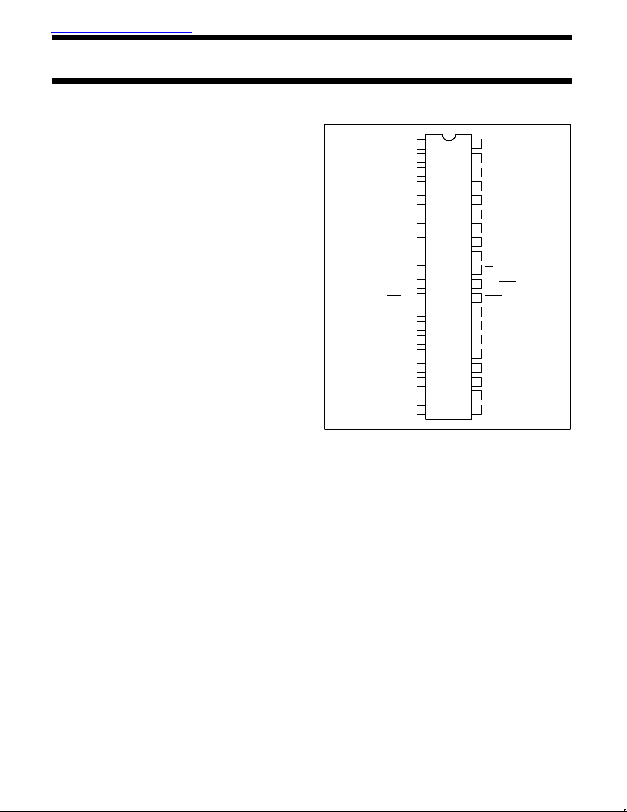
PIN CONFIGURATIONS
T2/P1.0
1
T2EX/P1.1
CEX0/P1.3
CEX1/P1.4
CEX2/P1.5
CEX3/P1.6
CEX4/P1.7
INT0
INT1
ECI/P1.2
RST
RxD/P3.0
TxD/P3.1
/P3.2
/P3.3
T0/P3.4
T1/P3.5
/P3.6
WR
RD
/P3.7
XTAL2
XTAL1
V
SS
2
3
4
5
6
7
8
9
10
11
12
13
14
15
16
17
18
19
20
DUAL
IN-LINE
PACKAGE
40
V
P0.0/AD0
39
38
P0.1/AD1
37
P0.2/AD2
36
P0.3/AD3
35
P0.4/AD4
34
P0.5/AD5
33
P0.6/AD6
32
P0.7/AD7
EA/V
31
30
ALE/PROG
29
PSEN
28
P2.7/A15
27
P2.6/A14
26
P2.5/A13
25
P2.4/A12
24
P2.3/A11
23
P2.2/A10
22
P2.1/A9
21
P2.0/A8
CC
PP
SU00021
1996 Aug 16 853-1729 17200
3-150
Philips Semiconductors Product specification
87L51F A/87L51FBCMOS single-chip 3.0V 8-bit microcontrollers
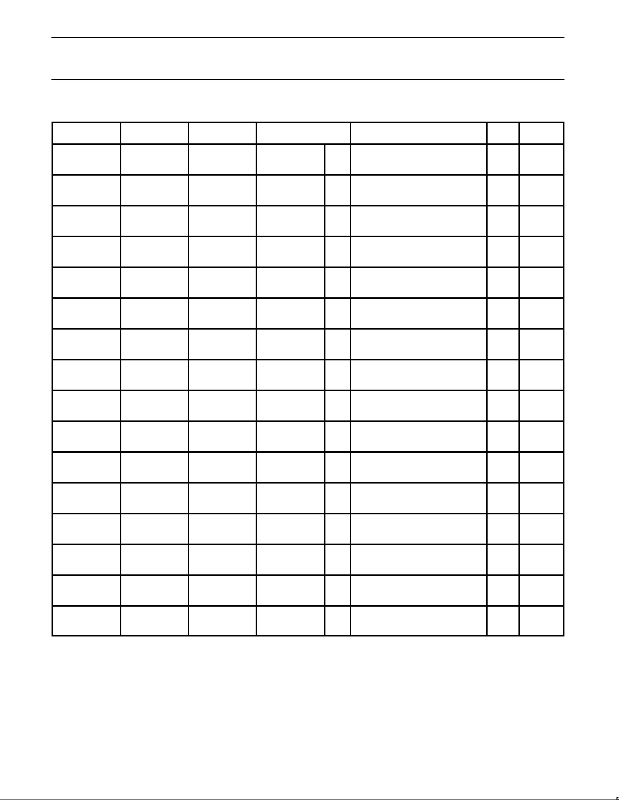
ORDERING INFORMATION
8k × 8
1
ROM
S83L51FA–4N40 S83L51FB–4N40 S87L51FA–4N40 S87L51FB–4N40 OTP
S83L51FA–4A44 S83L51FB–4A44 S87L51FA–4A44 S87L51FB–4A44 OTP
S83L51FA–4B44 S83L51FB–4B44 S87L51FA–4B44 S87L51FB–4B44 OTP
S83L51FA–5N40 S83L51FB–5N40 S87L51FA–5N40 S87L51FB–5N40 OTP
S87L51FA–5A44 S87L51FB–5A44 S87L51FA–5A44 S87L51FB–5A44 OTP
S83L51FA–5B44 S83L51FB–5B44 S87L51FA–5B44 S87L51FB–5B44 OTP
S83L51FA–7N40 S83L51FB–7N40 S87L51FA–7N40 S87L51FB–7N40 OTP
S83L51FA–7A44 S83L51FB–7A44 S87L51FA–7A44 S87L51FB–7A44 OTP
S83L51FA–8N40 S83L51FB–8N40 S87L51FA–8N40 S87L51FB–8N40 OTP
S83L51FA–8A44 S83L51FB–8A44 S87L51FA–8A44 S87L51FB–8A44 OTP
NOTES:
1. Contact Philips for information on low voltage Mask-ROM versions.
The 83C51FA and 83C51FB are specified for 2.7V–5.5V operation @ 16MHz.
2. OTP = One Time Programmable EPROM. UV = Erasable EPROM.
6k × 8
ROM
1
8k × 8
2
EPROM
S87L51FA–4F40 S87L51FB–4F40 UV
S87L51FA–4K44 S87L51FB–4K44 UV
S87L51FA–5F40 S87L51FB–5F40 UV
S87L51FA–7F40 S87L51FB–7F40 UV
S87L51FA–7K44 S87L51FB–7K44 UV
S87L51FA–8F40 S87L51FB–8F40 UV
16k × 8
EPROM
2
TEMPERA TURE RANGE °C
AND PACKAGE
0 to +70,
40-Pin Plastic Dual In-line Package
0 to +70,
40-Pin Ceramic Dual In-line Package
w/Window
0 to +70,
44-Pin Plastic Leaded Chip Carrier
0 to +70,
44-Pin Ceramic Leaded Chip Carrier
w/Window
0 to +70,
44-Pin Plastic Quad Flat Pack
–40 to +85,
40-Pin Plastic Dual In-line Package
–40 to +85,
40-Pin Ceramic Dual In-line Package
w/Window
–40 to +85,
44-Pin Plastic Leaded Chip Carrier
–40 to +85,
44-Pin Plastic Quad Flat Pack
0 to +70,
40-Pin Plastic Dual In-line Package
0 to +70,
40-Pin Ceramic Dual In-line Package
w/Window
0 to +70,
44-Pin Plastic Leaded Chip Carrier
0 to +70,
44-Pin Ceramic Leaded Chip Carrier
w/Window
–40 to +85,
40-Pin Plastic Dual In-line Package
–40 to +85,
40-Pin Ceramic Dual In-line Package
w/Window
–40 to +85,
44-Pin Plastic Leaded Chip Carrier
FREQ.
(MHz)
3.5
to
16
3.5
to
16
3.5
to
16
3.5
to
16
3.5
to
16
3.5
to
16
3.5
to
16
3.5
to
16
3.5
to
16
3.5
to
20
3.5
to
20
3.5
to
20
3.5
to
20
3.5
to
20
3.5
to
20
3.5
to
20
DWG.
#
SOT129-1
0590B
SOT187-2
1472A
SOT307-2
SOT129-1
0590B
SOT187-2
SOT307-2
SOT129-1
0590B
SOT187-2
1472A
SOT129-1
0590B
SOT187-2
1996 Aug 16
3-151

Philips Semiconductors Product specification
87L51F A/87L51FBCMOS single-chip 3.0V 8-bit microcontrollers
BLOCK DIAGRAM
P0.0–P0.7 P2.0–P2.7
PSEN
ALE/PROG
EA/V
PP
RST
PORT 0
DRIVERS
V
CC
V
SS
PSW
PORT 1
LATCH
PORT 0
LATCH
ALU
TMP1
RAM ADDR
REGISTER
B
REGISTER
TIMING
AND
CONTROL
INSTRUCTION
PD
RAM
ACC
TMP2
REGISTER
PORT 2
DRIVERS
PORT 2
LATCH
SFRs
TIMERS
P.C.A
STACK
POINTER
PORT 3
LATCH
ROM/EPROM
PROGRAM
ADDRESS
REGISTER
BUFFER
PC
INCRE-
MENTER
PROGRAM
COUNTER
DPTR
1996 Aug 16
OSCILLATOR
XTAL1 XTAL2
PORT 1
DRIVERS
P1.0–P1.7
3-152
PORT 3
DRIVERS
P3.0–P3.7
SU00022

Philips Semiconductors Product specification
87L51F A/87L51FBCMOS single-chip 3.0V 8-bit microcontrollers
CERAMIC AND PLASTIC LEADED CHIP CARRIER
PIN FUNCTIONS
6140
Pin Function
1 NC*
2 P1.0/T2
3 P1.1/T2EX
4 P1.2/ECI
5 P1.3/CEX0
6 P1.4/CEX1
7 P1.5/CEX2
8 P1.6/CEX3
9 P1.7/CEX4
10 RST
11 P3.0/RxD
12 NC*
13 P3.1/TxD
14 P3.2/INT0
15 P3.3/INT1
* DO NOT CONNECT
7
17
18 28
Pin Function
16 P3.4/T0
17 P3.5/T1
18 P3.6/WR
19 P3.7/RD
20 XTAL2
21 XTAL1
22 V
23 NC*
24 P2.0/A8
25 P2.1/A9
26 P2.2/A10
27 P2.3/A11
28 P2.4/A12
29 P2.5/A13
30 P2.6/A14
LCC
SS
39
29
Pin Function
31 P2.7/A15
32 PSEN
33 ALE/PROG
34 NC*
35 EA
/V
36 P0.7/AD7
37 P0.6/AD6
38 P0.5/AD5
39 P0.4/AD4
40 P0.3/AD3
41 P0.2/AD2
42 P0.1/AD1
43 P0.0/AD0
44 V
PP
CC
SU00023
PLASTIC QUAD FLAT PACK
PIN FUNCTIONS
44 34
1
PQFP
11
12 22
Pin Function
1 P1.5/CEX2
2 P1.6/CEX3
3 P1.7/CEX4
4 RST
5 P3.0/RxD
6 NC*
7 P3.1/TxD
8 P3.2/INT0
9 P3.3/INT1
10 P3.4/T0
11 P3.5/T1
12 P3.6/WR
13 P3.7/RD
14 XTAL2
15 XTAL1
* DO NOT CONNECT
Pin Function
16 V
SS
17 NC*
18 P2.0/A8
19 P2.1/A9
20 P2.2/A10
21 P2.3/A11
22 P2.4/A12
23 P2.5/A13
24 P2.6/A14
25 P2.7/A15
26 PSEN
27 ALE/PROG
28 NC*
29 EA
/V
30 P0.7/AD7
PP
33
23
Pin Function
31 P0.6/AD6
32 P0.5/AD5
33 P0.4/AD4
34 P0.3/AD3
35 P0.2/AD2
36 P0.1/AD1
37 P0.0/AD0
38 V
CC
39 NC*
40 P1.0/T2
41 P1.1/T2EX
42 P1.2/ECI
43 P1.3/CEX0
44 P1.4/CEX1
SU00024
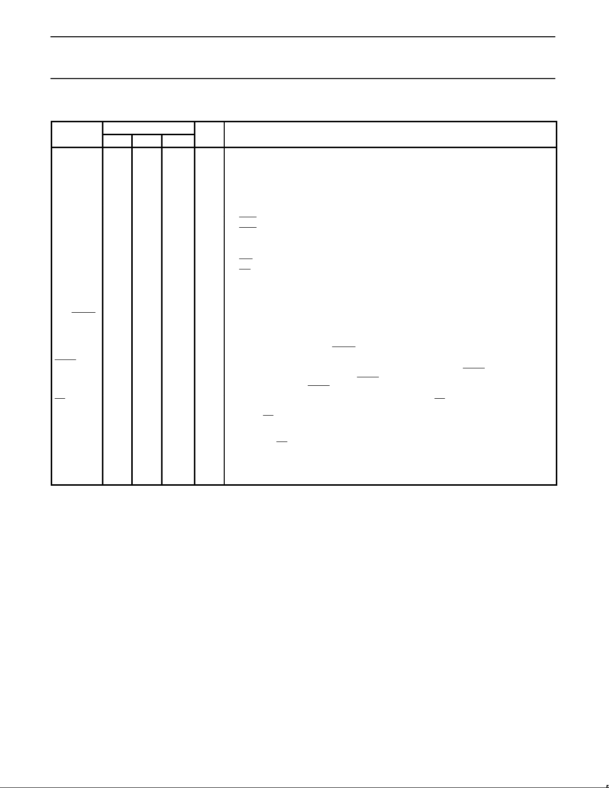
PIN DESCRIPTIONS
PIN NUMBER
MNEMONIC DIP LCC QFP TYPE NAME AND FUNCTION
V
SS
V
CC
P0.0–0.7 39–32 43–36 37–30 I/O Port 0: Port 0 is an open-drain, bidirectional I/O port. Port 0 pins that have 1s written to
P1.0–P1.7 1–8 2–9 40–44,
P2.0–P2.7 21–28 24–31 18–25 I/O Port 2: Port 2 is an 8-bit bidirectional I/O port with internal pull-ups. Port 2 pins that have 1s
20 22 16 I Ground: 0V reference.
40 44 38 I Power Supply: This is the power supply voltage for normal, idle, and power-down operation.
them float and can be used as high-impedance inputs. Port 0 is also the multiplexed
low-order address and data bus during accesses to external program and data memory. In
this application, it uses strong internal pull-ups when emitting 1s. Port 0 also outputs the
code bytes during program verification and receives code bytes during EPROM
programming. External pull-ups are required during program verification.
I/O Port 1: Port 1 is an 8-bit bidirectional I/O port with internal pull-ups. Port 1 pins that have 1s
1–3
written to them are pulled high by the internal pull-ups and can be used as inputs. As inputs,
port 1 pins that are externally pulled low will source current because of the internal pull-ups.
(See DC Electrical Characteristics: I
during program memory verification. Alternate functions include:
). Port 1 also receives the low-order address byte
IL
1 2 40 I T2 (P1.0): Timer/Counter 2 external count input/Clockout
2 3 41 I T2EX (P1.1): Timer/Counter 2 Reload/Capture/Direction Control
3 4 42 I ECI (P1.2): External Clock Input to the PCA
4 5 43 I/O CEX0 (P1.3): Capture/Compare External I/O for PCA module 0
5 6 44 I/O CEX1 (P1.4): Capture/Compare External I/O for PCA module 1
6 7 1 I/O CEX2 (P1.5): Capture/Compare External I/O for PCA module 2
7 8 2 I/O CEX3 (P1.6): Capture/Compare External I/O for PCA module 3
8 9 3 I/O CEX4 (P1.7): Capture/Compare External I/O for PCA module 4
written to them are pulled high by the internal pull-ups and can be used as inputs. As inputs,
port 2 pins that are externally being pulled low will source current because of the internal
pull-ups. (See DC Electrical Characteristics: I
during fetches from external program memory and during accesses to external data memory
). Port 2 emits the high-order address byte
IL
that use 16-bit addresses (MOVX @DPTR). In this application, it uses strong internal
pull-ups when emitting 1s. During a c c esses to exter n al data memor y that use 8-bit addresses
(MOV @Ri), port 2 emits the contents of the P2 special function register. Some Port 2 pins
receive the high order address bits during EPROM programming and verification.
1996 Aug 16
3-153
Philips Semiconductors Product specification
87L51F A/87L51FBCMOS single-chip 3.0V 8-bit microcontrollers
PIN DESCRIPTIONS (Continued)
PIN NUMBER
MNEMONIC DIP LCC QFP TYPE NAME AND FUNCTION
P3.0–P3.7 10–17 11,
RST 9 10 4 I Reset: A high on this pin for two machine cycles while the oscillator is running, resets the
ALE/PROG 30 33 27 I/O Address Latch Enable/Program Pulse: Output pulse for latching the low byte of the
PSEN 29 32 26 O Program Store Enable: The read strobe to external program memory. When the
EA/V
PP
XTAL1 19 21 15 I Crystal 1: Input to the inverting oscillator amplifier and input to the internal clock generator
XTAL2 18 20 14 O Crystal 2: Output from the inverting oscillator amplifier.
NOTE:
To avoid “latch-up” effect at power-on, the voltage on any pin at any time must not be higher than V
13–195,7–13
10 11 5 I RxD (P3.0): Serial input port
11 13 7 O TxD (P3.1): Serial output port
12 14 8 I INT0 (P3.2): External interrupt
13 15 9 I INT1 (P3.3): External interrupt
14 16 10 I T0 (P3.4): Timer 0 external input
15 17 11 I T1 (P3.5): Timer 1 external input
16 18 12 O WR (P3.6): External data memory write strobe
17 19 13 O RD (P3.7): External data memory read strobe
31 35 29 I External Access Enable/Programming Supply Voltage: EA must be externally held low
I/O Port 3: Port 3 is an 8-bit bidirectional I/O port with internal pull-ups. Port 3 pins that have 1s
written to them are pulled high by the internal pull-ups and can be used as inputs. As inputs,
port 3 pins that are externally being pulled low will source current because of the pull-ups.
(See DC Electrical Characteristics: I
family, as listed below:
device. An internal diffused resistor to V
capacitor to V
address during an access to external memory. In normal operation, ALE is emitted at a
constant rate of 1/6 the oscillator frequency, and can be used for external timing or clocking.
Note that one ALE pulse is skipped during each access to external data memory. This pin is
also the program pulse input (PROG
87L51FA/FB is executing code from the external program memory, PSEN
each machine cycle, except that two PSEN
external data memory. PSEN
to enable the device to fetch code from external program memory locations 0000H and
1FFFH. If EA
program counter contains an address greater than 1FFFH. This pin also receives the
12.75V programming supply voltage (V
programmed, EA
circuits.
.
CC
is held high, the device executes from internal program memory unless the
will be internally latched on Reset.
). Port 3 also serves the special features of the 80C51
IL
permits a power-on reset using only an external
SS
) during EPROM programming.
is not activated during fetches from internal program memory.
activations are skipped during each access to
) during EPROM programming. If security bit 1 is
PP
+ 0.5V or VSS – 0.5V , respectively.
CC
is activated twice
TIMER 2
This is a 16-bit up or down counter, which can be operated as either
a timer or event counter. It can be operated in one of three different
modes (autoreload, capture or as the baud rate generator for the
UART).
In the autoreload mode the Timer can be set to count up or down by
setting or clearing the bit DCEN in the T2CON Special Function
Register. The SFR’ s RCAP2H and RCAP2L are used to reload the
Timer upon overflow or a 1-to-0 transition on the T2EX input (P1.1).
In the Capture mode Timer 2 can either set TF2 and generate an
interrupt or capture its value. To capture Timer 2 in response to a
1-to-0 transition on the T2EX input, the EXEN2 bit in the T2CON
must be set. Timer 2 is then captured in SFR’s RCAP2H and
RCAP2L.
As the baud rate generator, Timer 2 is selected by setting TCLK
and/or RCLK in T2CON. As the baud rate generator Timer 2 is
incremented at
1996 Aug 16
1
/2 the oscillator frequency.
ENHANCED UART
The 87L51FA/FB UART has all of the capabilities of the standard
80C51 UART plus Framing Error Detection and Automatic Address
Recognition. As in the 80C51, all four modes of operation are
supported as well as the 9th bit in modes 2 and 3 that can be used
to facilitate multiprocessor communication.
The Framing Error Detection allows the UART to look for missing
stop bits. If a Stop bit is missing, the FE bit in the SCON SFR is set.
The FE bit can be checked after each transmission to detect
communication errors. The FE bit can only be cleared by software
and is not affected by a valid stop bit.
Automatic Address Recognition is used to reduce the CPU service
time for the serial port. The CPU only needs to service the UART
when it is addressed and, with this done by the on-chip circuitry, the
need for software overhead is greatly reduced. This mode works
similar to the 9-bit communication mode, except that it uses only 8
bits and the Stop bit is used to cause the RI bit to be set. There are
two SFRs associated with this mode. They are SADDR, which holds
the slave address and SADEN, which contains a mask that allows
selective masking of the slave address so that broadcast addresses
can be used.
3-154

Philips Semiconductors Product specification
87L51F A/87L51FBCMOS single-chip 3.0V 8-bit microcontrollers
PROGRAMMABLE COUNTER ARRAY
The PCA is a sophisticated free-running 16 bit Timer/Counter that
drives 5 modules that can be individually configured as Capture
inputs, software timers, high speed outputs, or pulse width
modulated outputs. In addition, module 4 can be configured as a
software controlled watchdog timer.
The Timer portion of the PCA can be configured to run in one of four
different modes. The modes are:
oscillator frequency , Timer 0 overflows, or from the ECI input.
For the Capture/Compare mode each of the modules has a pair of
registers associated with it called CCAPnH and CCAPnL (where
n = 0, 1, 2, 3, 4 depending on the module). Both positive and
negative transitions can be captured. This means that the PCA has
the flexibility to measure phase differences, duty cycles, pulse
widths and a wide variety of other digital pulse characteristics.
In the 16-bit software timer mode each of the modules can generate
an interrupt upon a compare.
For applications that require accurate pulse widths and edges the
PCA modules can be used as High Speed Outputs (HSO). The PCA
toggles the appropriate CEXn pin when there is a match between
the PCA timer and the modules compare registers.
The pulse width modulator mode for the PCA allows the conversion
of digital information into analog signals. Each of the 5 modules can
be used in this mode. The frequency of the PWM depends on the
clock source for the PCA. The 8-bit PWM output is generated by
comparing the low byte of the PCA (CL) with the module’s CCAPnL
SFR. When CL < CCAPnL, the output is high. When CL > CCAPnL,
the output is low.
1
/2 the oscillator frequency, 1/4 the
POWER OFF FLAG
The Power Off Flag (POF) is set by on-chip circuitry when the V
level on the 87L51FA/FB rises from 0 to 3.3V. The POF bit can be
set or cleared by software allowing a user to determine if the reset is
the result of a power-on or a warm start after powerdown. The V
level must remain above 2.0V for the POF to remain unaffected by
the V
level.
CC
CC
CC
OSCILLA T OR CHARACTERISTICS
XTAL1 and XTAL2 are the input and output, respectively , of an
inverting amplifier . The pins can be configured for use as an on-chip
oscillator.
To drive the device from an external clock source, XTAL1 should be
driven while XTAL2 is left unconnected. There are no requirements
on the duty cycle of the external clock signal, because the input to
the internal clock circuitry is through a divide-by-two flip-flop.
However, minimum and maximum high and low times specified in
the data sheet must be observed.
Reset
A reset is accomplished by holding the RST pin high for at least two
machine cycles (24 oscillator periods), while the oscillator is running.
To insure a good power-on reset, the RST pin must be high long
enough to allow the oscillator time to start up (normally a few
milliseconds) plus two machine cycles. At power-on, the voltage on
and RST must come up at the same time for a proper start-up.
V
CC
Idle Mode
In the idle mode, the CPU puts itself to sleep while all of the on-chip
peripherals stay active. The instruction to invoke the idle mode is the
last instruction executed in the normal operating mode before the
idle mode is activated. The CPU contents, the on-chip RAM, and all
of the special function registers remain intact during this mode. The
idle mode can be terminated either by any enabled interrupt (at
which time the process is picked up at the interrupt service routine
and continued), or by a hardware reset which starts the processor in
the same manner as a power-on reset.
Power-Down Mode
To save even more power, a Power Down mode can be invoked by
software. In this mode, the oscillator is stopped and the instruction
that invoked Power Down is the last instruction executed. The
on-chip RAM and Special Function Registers retain their values until
the Power Down mode is terminated.
On the 87L51FA/FB either a hardware reset or external interrupt can
use an exit from Power Down. Reset redefines all the SFRs but
does not change the on-chip RAM. An external interrupt allows both
the SFRs and the on-chip RAM to retain their values.
To properly terminate Power Down the reset or external interrupt
should not be executed before V
operating level and must be held active long enough for the
oscillator to restart and stabilize (normally less than 10ms).
With an external interrupt, INT0 and INT1 must be enabled and
configured as level-sensitive. Holding the pin low restarts the
oscillator but bringing the pin back high completes the exit. Once the
interrupt is serviced, the next instruction to be executed after RETI
will be the one following the instruction that put the device into
Power Down.
is restored to its normal
CC
Design Consideration
•When the idle mode is terminated by a hardware reset, the device
normally resumes program execution, from where it left off, up to
two machine cycles before the internal rest algorithm takes
control. On-chip hardware inhibits access to internal RAM in this
event, but access to the port pins is not inhibited. To eliminate the
possibility of an unexpected write when Idle is terminated by reset,
the instruction following the one that invokes Idle should not be
one that writes to a port pin or to external memory.
ONCE Mode
The ONCE (“On-Circuit Emulation”) Mode facilitates testing and
debugging of systems using the 87L51FA/FB without the
87L51FA/FB having to be removed from the circuit. The ONCE
Mode is invoked by:
1. Pull ALE low while the device is in reset and PSEN
2. Hold ALE low as RST is deactivated.
While the device is in ONCE Mode, the Port 0 pins go into a float
state, and the other port pins and ALE and PSEN
high. The oscillator circuit remains active. While the 87L51FA/FB is
in this mode, an emulator or test CPU can be used to drive the
circuit. Normal operation is restored when a normal reset is applied.
is high;
are weakly pulled
1996 Aug 16
3-155
 Loading...