

Philips 80cl410 DATASHEETS

INTEGRATED CIRCUITS
80CL410/83CL410
Low voltage/low power single-chip
2
8-bit microcontroller with I
Product specification 1995 Jan 20
IC20 Data Handbook
C

Philips Semiconductors Product specification
Numb
Low voltage/low power single-chip
2
8-bit microcontroller with I
DESCRIPTION
The 80CL410/83CL410 (hereafter generically
referred to as 8XCL410) is manufactured in
an advanced CMOS process that allows the
part to operate at supply voltages down to
1.8V and oscillator frequencies down to DC.
The 8XCL410 has the same instruction set
as the 80C51.
The 8XCL410 features a 4k byte ROM
(83CL410), 128 bytes RAM (both ROM and
RAM are externally expandable to 64k
bytes), four 8-bit ports, two 16-bit
timer/counters, an I
thirteen source, two priority level nested
interrupt structure, and on-chip oscillator
circuitry suitable for quartz crystal, ceramic
resonator, RC, or LC.
The 8XCL410 has two reduced power modes
that are the same as those on the standard
80C51. The special reduced power feature of
this part is that it can be stopped and then
restarted. Running from an external clock
source, the clock can be stopped and after a
period of time restarted. The 8XCL410 will
resume operation from where it was when the
code stopped with no loss of internal state,
RAM contents, or Special Function Register
contents. If the internal oscillator is used the
part cannot be stopped and started, but the
power-down mode, which can be terminated
via an interrupt, can be used to achieve
similar power savings and then restart
without loss of on-chip RAM and Special
Function Register values.
2
C serial interface, a
C
FEA TURES
•Single supply voltage 1.8V to 6.0V
•Frequency from DC to 12MHz
•80C51 based architecture
– 4k × 8 ROM (64k external)
– 128 × 8 RAM (64k external)
– Four 8-bit I/O ports
– Two 16-bit timer/counters
– A thirteen-source, two-level, nested
priority interrupt structure
– 10 external interrupts
•Fully static 80C51 CPU
2
•I
C Serial Interface
•Two power control modes
– Idle mode
– Power-down mode – can be terminated
by reset or external interrupt
•Wake-up via external interrupts at port 1
•Single supply voltage 1.8V to 6.0V
•Frequency range of DC to 12MHz
•On-chip oscillator (quartz crystal, ceramic
resonator, RC, LC)
•Very low power consumption
•Operating temperature range:
–40 to +85°C
80CL410/83CL410
PIN CONFIGURATION
INT2/P1.0
INT3/P1.1
INT4/P1.2
INT5/P1.3
INT6/P1.4
INT7/P1.5
SCL/INT8/P1.6
SDA/INT9/P1.7
INT0
INT1/P3.3
SEE NEXT PAGE FOR QFP PIN FUNCTIONS.
/P3.2
T0/P3.4
T1/P3.5
/P3.6
WR
RD
XTAL2
XTAL1
V
1
11
1
2
3
4
5
6
7
8
9
RST
10
P3.0
11
P3.1
12
13
14
15
16
/P3.7
17
18
19
20
SS
44 34
12 22
DIP
VSO
QFP
40
39
38
37
36
35
34
33
32
31
30
29
28
27
26
25
24
23
22
21
V
DD
P0.0/AD0
P0.1/AD1
P0.2/AD2
P0.3/AD3
P0.4/AD4
P0.5/AD5
P0.6/AD6
P0.7/AD7
EA
ALE
PSEN
P2.7/A15
P2.6/A14
P2.5/A13
P2.4/A12
P2.3/A11
P2.2/A10
P2.1/A9
P2.0/A8
33
23
ORDERING CODE
PHILIPS PART ORDER NUMBER
PART MARKING
ROMless ROM ROMless ROM
P80CL410HFP P83CL410HFP P80CL410HF N P83CL410HF N
P80CL410HFT P83CL410HFT P80CL410HF D P83CL410HF D
P83CL410HFH
NOTE:
1. Parts ordered by the Philips North America part number will be marked with the Philips part marking.
For emulation purposes, the P85CL000 (Piggyback version) with 256 bytes of RAM is recommended.
1995 Jan 20
PHILIPS NORTH AMERICA
PART ORDER NUMBER
1
TEMPERATURE °C
AND PACKAGE
–40 to +85,
40-Pin Plastic Dual In-line Package
–40 to +85,
40-Pin Plastic Very Small Outline
Package
–40 to +85,
44-Pin Plastic Quad Flat Pack
2
Drawing
FREQUENCY
er
32kHZ to 12MHz SOT129-1
32kHZ to 12MHz SOT158-1
32kHZ to 12MHz SOT307-2
Philips Semiconductors Product specification
Low voltage/low power single-chip
2
8-bit microcontroller with I
PLASTIC QUAD FLAT PACK
PIN FUNCTIONS
44 34
1
QFP
11
12 22
Pin Function Pin Function
1 P1.5/INT7 23 P2.5/A13
2 P1.6/INT8/SCL 24 P2.6/A14
3 P1.7/INT9/SDA 25 P2.7/A15
4 RST 26 PSEN
5 P3.0 27 ALE
6 NC 28 NC
7 P3.1 29 EA
8 P3.2/INT0 30 P0.7/AD7
9 P3.3/INT1 31 P0.6/AD6
10 P3.4/T0 32 P0.5/AD5
11 P3.5/T1 33 P0.4/AD4
12 P3.6/WR 34 P0.3/AD3
13 P3.7/RD 35 P0.2/AD2
14 XTAL2 36 P0.1/AD1
15 XTAL1 37 P0.0/AD0
16
V
SS
17 NC 39 NC
18 P2.0/A8 40 P1.0/INT2
19 P2.1/A9 41 P1.1/INT3
20 P2.2/A10 42 P1.2/INT4
21 P2.3/A11 43 P1.3/INT5
22 P2.4/A12 44 P1.4/INT6
38
33
23
V
DD
C
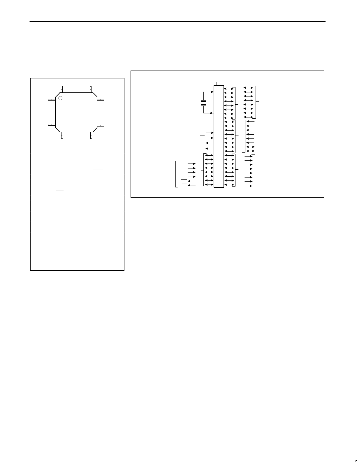
LOGIC SYMBOL
XTAL1
XTAL2
RST
EA
PSEN
ALE
INT0
INT1
T0
T1
WR
RD
Alternate Functions
Port 3
80CL410/83CL410
V
V
SS
DD
Address and
Port 0
Port 1Port 2
Data Bus
INT2
INT3
INT4
INT5
INT6
INT7
INT8/SCL
INT9/SDA
Address Bus
1995 Jan 20
3
Philips Semiconductors Product specification
Low voltage/low power single-chip
2
8-bit microcontroller with I
BLOCK DIAGRAM
FREQUENCY
REFERENCE
XTAL2 XTAL1
OSCILLATOR
AND
TIMING
CPU
10 3
INTERNAL
INTERRUPTS
C
PROGRAM
MEMORY
(4K × 8 ROM)
64K BYTE BUS
EXPANSION
CONTRTOL
DATA
MEMORY
(128 × 8 RAM)
PROGRAMMABLE I/O
80CL410/83CL410
COUNTER (1)
T0 T1
TWO 16-BIT
TIMER/EVENT
COUNTERS
I2C-BUS SERIAL I/O
EXTERNAL
INTERRUPTS
(1) Pins shared with parallel port pins.
(1)
CONTROL
PARALLEL PORTS,
ADDRESS/DATA BUS
AND I/O PINS
SDA SCL
(1)
1995 Jan 20
4
Philips Semiconductors Product specification
Low voltage/low power single-chip
2
8-bit microcontroller with I
C
PIN DESCRIPTION
PIN NO.
MNEMONIC
V
SS
V
DD
P0.0–0.7 30–37 39–32 I/O Port 0: Port 0 is an open-drain, bidirectional I/O port. Port 0 pins that have 1s written
P1.0–P1.7 40–44
7 I/O SCL (P1.6): I2C serial bus clock.
8 I/O SDA (P1.7): I2C serial bus data.
1–8 I INT2–INT9 (P1.0–P1.7): Additional external interrupts.
P2.0–P2.7 18–25 21–28 I/O Port 2: Port 2 is an 8-bit bidirectional I/O port with internal pull-ups. Port 2 pins that
P3.0–P3.7 5, 7–13 10–17 I/O Port 3: Port 3 is an 8-bit bidirectional I/O port with internal pull-ups. Port 3 pins that
RST 4 9 I Reset: A high on this pin for two machine cycles while the oscillator is running, resets
ALE 27 30 O Address Latch Enable: Output pulse for latching the low byte of the address during
PSEN 26 29 O Program Store Enable: The read strobe to external program memory. When the
EA 29 31 I External Access Enable: EA must be externally held low to enable the device to
XTAL1 15 19 I Crystal 1: Input to the inverting oscillator amplifier and input for an external clock
XTAL2 14 18 O Crystal 2: Output from the inverting oscillator amplifier.
QFP
16 20 I Ground: 0V reference.
38 40 I Power Supply: This is the power supply voltage for normal, idle, and power-down
1–3
8 12 I INT0 (P3.2): External interrupt 0
9 13 I INT1 (P3.3): External interrupt 1
10 14 I T0 (P3.4): Timer 0 external input
11 15 I T1 (P3.5): Timer 1 external input
12 16 O WR (P3.6): External data memory write strobe
13 17 O RD (P3.7): External data memory read strobe
DIL40/
VSO40
1–8 I/O Port 1: Port 1 is an 8-bit bidirectional I/O port with internal pull-ups. Port 1 pins that
TYPE NAME AND FUNCTION
operation.
to them float and can be used as high-impedance inputs. Port 0 is also the multiplexed
low-order address and data bus during accesses to external program and data
memory. In this application, it uses strong internal pull-ups when emitting 1s.
have 1s written to them are pulled high by the internal pull-ups and can be used as
inputs. As inputs, port 1 pins that are externally pulled low will source current because
of the internal pull-ups. (See DC Electrical Characteristics: I
include:
have 1s written to them are pulled high by the internal pull-ups and can be used as
inputs. As inputs, port 2 pins that are externally being pulled low will source current
because of the internal pull-ups. (See DC Electrical Characteristics: I
the high-order address byte during fetches from external program memory and during
accesses to external data memory that use 16-bit addresses (MOVX @DPTR). In this
application, it uses strong internal pull-ups when emitting 1s. During accesses to
external data memory that use 8-bit addresses (MOV @Ri), port 2 emits the contents
of the P2 special function register.
have 1s written to them are pulled high by the internal pull-ups and can be used as
inputs. As inputs, port 3 pins that are externally being pulled low will source current
because of the pull-ups. (See DC Electrical Characteristics: I
special features of the 80C51 family, as listed below:
the device. An internal diffused resistor to V
external capacitor to V
an access to external memory. In normal operation, ALE is emitted at a constant rate
of 1/6 the oscillator frequency, and can be used for external timing or clocking. Note
that one ALE pulse is skipped during each access to external data memory.
device is executing code from the external program memory, PSEN
each machine cycle, except that two PSEN
access to external data memory. PSEN
program memory.
fetch code from external program memory locations 0000H to 0FFFH. If EA
high, the device executes from internal program memory unless the program counter
contains an address greater than 0FFFH.
source.
DD
.
SS
activations are skipped during each
is not activated during fetches from internal
80CL410/83CL410
). Additional functions
IL
). Port 2 emits
IL
). Port 3 also serves the
IL
permits a power-on reset using only an
is activated twice
is held
1995 Jan 20
5
Philips Semiconductors Product specification
Low voltage/low power single-chip
2
8-bit microcontroller with I
C
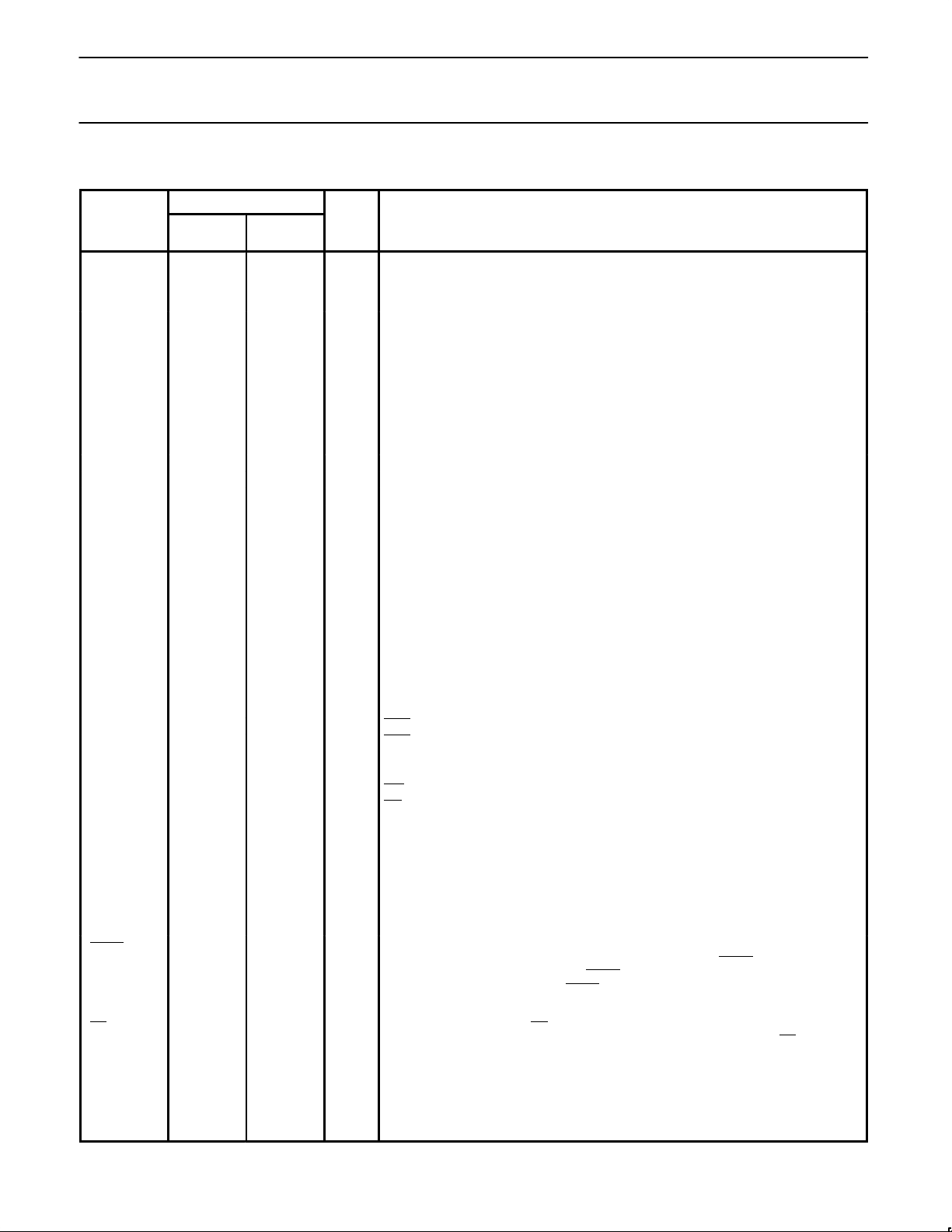
Table 1. 8XCL410 Special Function Registers
SYMBOL DESCRIPTION
ACC* Accumulator E0H E7 E6 E5 E4 E3 E2 E1 E0 00H
B* B register F0H F7 F6 F5 F4 F3 F2 F1 F0 00H
DPTR:
DPH
DPL
IP0*# Interrupt priority 0 B8H – – PS1 – PT1 PX1 PT0 PX0 xx000000B
IP1*# Interrupt priority 1 F8H PX9 PX8 PX7 PX6 PX5 PX4 PX3 PX2 00H
IEN0*# Interrupt enable 0 A8H EA – ES1 – ET1 EX1 ET0 EX0 00H
IEN1*# Interrupt enable 1 E8H EX9 EX8 EX7 EX6 EX5 EX4 EX3 EX2 00H
IRQ1*# Interrupt request flag C0H IQ9 IQ8 IQ7 IQ6 IQ5 IQ4 IQ3 IQ2 00H
IX1# Interrupt polarity E9H 00H
P0* Port 0 80H 87 86 85 84 83 82 81 80 FFH
P1* Port 1 90H 97 96 95 94 93 92 91 90 FFH
P2* Port 2 A0H A7 A6 A5 A4 A3 A2 A1 A0 FFH
P3* Port 3 B0H B7 B6 B5 B4 B3 B2 B1 B0 FFH
Data pointer
(2 bytes):
High byte
Low byte
DIRECT
ADDRESS
83H
82H
BIT ADDRESS, SYMBOL, OR ALTERNATIVE PORT FUNCTION
MSB LSB
BF BE BD BC BB BA B9 B8
FF FE FD FC FB FA F9 F8
AF AE AD AC AB AA A9 A8
EF EE ED EC EB EA E9 E8
C7 C6 C5 C4 C3 C2 C1 C0
80CL410/83CL410
RESET
VALUE
00H
00H
PCON Power control 87H SMOD – – – GF1 GF0 PD IDL 0xxx0000B
D7 D6 D5 D4 D3 D2 D1 D0
PSW* Program status word D0H CY AC F0 RS1 RS0 OV – P 00H
S1ADR# Slave address DBH 00H
DF DE DD DC DB DA D9 D8
S1CON*# Serial control D8H – ENS1 STA STO SI AA CR1 CR0 x0000000B
S1DAT#
S1STA#
SP Stack pointer 81H 07H
TCON* Timer/counter con-
TMOD Timer/counter mode 89H GATE C/T M1 M0 GATE C/T M1 M0 00H
TH0 Timer 0 high byte 8CH 00H
TH1 Timer 1 high byte 8DH 00H
TL0 Timer 0 low byte 8AH 00H
TL1 Timer 1 low byte 8BH 00H
* SFRs are bit addressable.
# SFRs are modified from or added to the 80C51 SFRs.
Serial data
Serial status
trol
DAH
D9H
8F 8E 8D 8C 8B 8A 89 88
88H TF1 TR1 TF0 TR0 IE1 IT1 IE0 IT0 00H
00H
11111000B
1995 Jan 20
6
Philips Semiconductors Product specification
Low voltage/low power single-chip
2
8-bit microcontroller with I
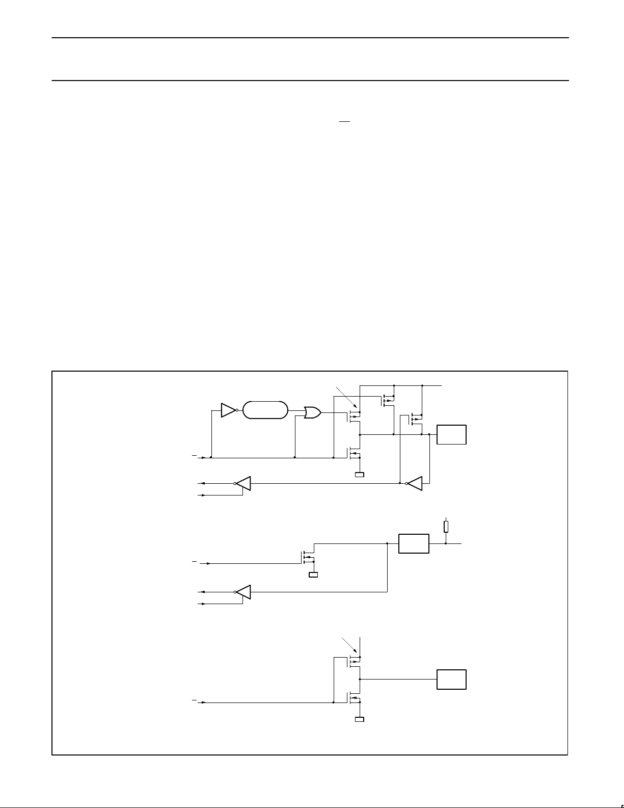
PORT OPTIONS
The pins of port 1 (not P1.6/SCL or
P1.7/SDA), port 2, and port 3 may be
individually configured with one of the
following port options (see Figure 1):
Option 1: Standard Port—
quasi-bidirectional I/O with pull-up.
The strong booster pull-up p1 is
turned on for two oscillator periods
after a 0-to-1 transition in the port
latch. See Figure 1(a).
Option 2: Open Drain—quasi-bidirectional
I/O with n-channel open drain
output. Use as an output requires
the connection of an external
pull-up resistor. See Figure 1(b).
Option 3: Push-Pull—output with drive
capability in both polarities. Under
this option, pins can only be used
as outputs. See Figure 1(c).
The definition of port options for port 0 is
slightly different.
C
Two cases have to be examined. First,
accesses to external memory (EA
access above the built-in memory boundary),
and second, I/O accesses.
External Memory Accesses
Option 1: True 0 and 1 are written as
Option 2: An external pull-up resistor is
Option 3: Not allowed for external memory
I/O Accesses
Option 1: When writing a 1 to the port latch,
= 0 or
address to the external memory
(strong pull-up is used).
needed for external accesses.
accesses as the port can only be
used as output.
the strong pull-up p1 will be on for
two oscillator periods. No weak
pull-up exists. Without an external
pull-up, this option can be used as
a high-impedance input.
80CL410/83CL410
Option 2: Open drain—quasi-bidirectional
I/O with n-channel open drain
output. Use as an output requires
the connection of an external
pull-up resistor. See Figure 1(c).
Option 3: Push-Pull—output with drive
capability in both polarities. Under
this option, pins can only be used
as outputs.
Individual mask selection of the post-reset
state is available on any of the above pins.
Make your selection by appending “S” or “R”
to option 1, 2, or 3 above (e.g., 1S for a
standard I/O to be set after RESET or 2R for
an open-drain I/O to be reset after RESET.
Option S: Set—after reset, this pin will be
initialized High.
Option R: Reset—after reset, this pin will be
initialized Low.
(a)
(b)
(c)
FROM PORT LATCH
INPUT DATA
READ PORT PIN
FROM PORT LATCH
INPUT DATA
READ PORT PIN
STRONG PULL-UP
TWO OSCILLATOR PERIODS
P1
Q
INPUT
BUFFER
Q
INPUT
BUFFER
STRONG PULL-UP
N
N
+5V
P1
P2
I/O PIN
+5V
P3
I/O PIN
+5V
EXTERNAL
PULL-UP
I/O PIN
FROM PORT LATCH
1995 Jan 20
Q
N
Figure 1. Ports
7

Philips Semiconductors Product specification
Low voltage/low power single-chip
2
8-bit microcontroller with I
POWER-DOWN MODE
The instruction setting PCON.1 is the last
executed prior to going into the power-down
mode. In power-down mode, the oscillator is
stopped. The contents of the the on-chip
RAM and SFRs are preserved. The port pins
output the values held by their respective
SFRs. ALE and PSEN
In the power-down mode, V
reduced to minimize power consumption.
However, the supply voltage must not be
reduced until the power-down mode is active,
and must be restored before the hardware
reset is applied and frees the oscillator. Reset
must be held active until the oscillator has
restarted and stabilized.
From the power-down mode the part can be
restarted by using either the wake-up mode
or the Reset Mode.
Wake-Up Mode
Setting both PD and IDL bits in the PCON
register forces the controller into the
power-down mode. Setting both bits enable
the controller to be woken-up from the
power-down mode via either an enabled
external interrupt INT2–INT9, or a reset
operation.
An external interrupt for an enabled interrupt
INT2–INT9 at port 1 starts both the oscillator
and the delay counter. To ensure that the
oscillator is stable before the controller
restarts, the internal clock will remain inactive
for 1536 oscillator periods after the interrupt
are held low.
may be
DD
C
is detected. This is controlled by the on-chip
delay counter. After this, the PD flag will be
reset, the controller is now in the Idle mode
and the interrupt will be handled in the normal
way.
Reset Mode
Setting only the PD bit in the PCON register
again forces the controller into the
power-down mode, but in this case it can
only be restored to normal operation with a
direct reset operation.
To restore normal operation, the RESET pin
has to be kept High for a minimum of 24
oscillator periods. The on-chip delay counter
is inactive. The user has to insure that the
oscillator is stable before any operation is
attempted. Figure 2 illustrates the two
possibilities for wake-up.
IDLE MODE
The instruction that sets PCON.0 is the last
instruction executed before going into idle
mode. In idle mode, the internal clock is
stopped for the CPU, but not for the interrupt,
timer, and serial port functions. The CPU
status is preserved along with the stack
pointer, program counter, program status
word and accumulator. The RAM and all
other registers maintain their data during idle
mode. The port pins retain the logical states
they held at idle mode activation. ALE and
PSEN
80CL410/83CL410
There are two methods used to terminate the
idle mode. Activation of any interrupt will
cause PCON to be cleared by hardware;
terminating idle mode. The interrupt is
serviced, and following the instruction RETI,
the next instruction to be executed will be the
one following the instruction that put the
device in the the idle mode.
Flag bits GF0 and GF1 can be used to
determine whether the interrupt was received
during normal execution or idle mode. For
example, the instruction that writes to
PCON.0 can also set or clear one or both flag
bits. When idle mode is terminated by an
interrupt, the service routine can examine the
status of the flag bits.
The second method of terminating the idle
mode is with an external hardware reset.
Since the oscillator is still running, the
hardware reset is required to be active for
only two machine cycles to complete the
reset operation. Reset redefines all SFRs,
but does not affect the state of the on-chip
RAM.
The status of the external pins during idle and
power-down mode is shown in Table 2. If the
power-down mode is activated while
accessing external memory, port data held in
the special function register P2 is restored to
port 2. If the data is a logic 1, the port pin is
held high during the power-down mode.
hold at the logic high level.
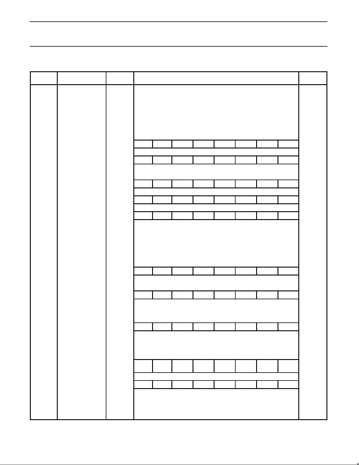
Table 2. External Pin Status During Idle and Power-Down Modes
MODE PROGRAM MEMORY ALE PSEN PORT 0 PORT 1 PORT 2 PORT 3
Idle Internal 1 1 Data Data Data Data
Idle External 1 1 Floating Data Address Data
Power-down Internal 0 0 Data Data Data Data
Power-down External 0 0 Floating Data Data Data
EXTERNAL INTERRUPT
1995 Jan 20
POWER-DOWN
RESET PIN
OSCILLATOR
DELAY COUNTER
1536 PERIODS
Figure 2. Wake-Up Operation
8
> 24 PERIODS
Philips Semiconductors Product specification
Low voltage/low power single-chip
2
8-bit microcontroller with I
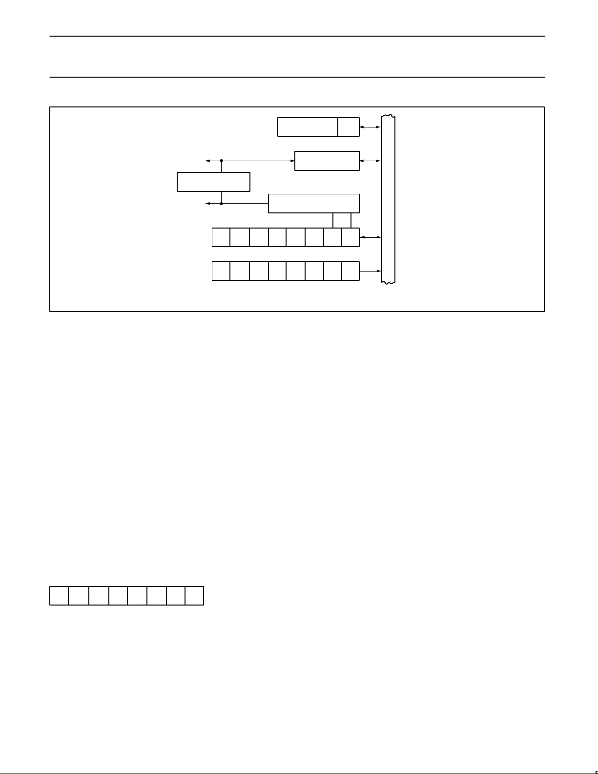
SDA
ARBITRATION LOGIC
SCL
I2C-BUS SERIAL I/O
The serial port supports the twin line I2C-bus.
2
The I
C-bus consists of a data line (SDA)
and a clock line (SCL). These lines also
function as I/O port lines P1.7 and P1.6
respectively. The system is unique because
data transport, clock generation, address
recognition and bus control arbitration are all
controlled by hardware. The I
I/O has complete autonomy in byte handling
and operates in four modes:
– Master transmitter
– Master receiver
– Slave transmitter
– Slave receiver
These functions are controlled by the S1CON
register. S1STA is the status register whose
contents may also be used as a vector to
various service routines. S1DAT is the data
shift register and S1ADR the slave address
register. Slave address recognition is
performed by hardware.
S1CON (D8H)
Serial control register
CR2 ENS1 STA STO SI AA CR1 CR0
CR0, CR1, CR2
These three bits determine the
serial clock frequency when SIO
is in a master mode.
2
C-bus serial
C
76 5 43 2 1 0
S1CON
76 5 43 2 1 0
S1STA
AA Assert acknowledge bit. When
SI SIO interrupt flag. When the SI
SLAVE ADDRESS
S1ADR
SHIFT REGISTER
S1DAT
BUS CLOCK GENERATOR
GC
Figure 3. Serial I/O
the AA flag is set, an
acknowledge (low level to SDA)
will be returned during the
acknowledge clock pulse on the
SCL line when:
– own slave address is received
– general call address is
received (S1ADR.0 = 1)
– data byte received while
device is programmed as
master
– data byte received while
device is selected slave
With AA = 0, no acknowledge will
be returned. Consequently, no
interrupt is requested when the
“own slave address” or general
call address is received.
flag is set, an acknowledge is
returned after any one of the
following conditions:
– a start condition is generated
in master mode
– own slave address received
during AA = 1
– general call address received
while S1ADR.0 and AA = 1
– data byte received or
transmitted in master mode
(even if arbitration is lost)
– data byte received or
transmitted as selected slave
– stop or start condition received
as selected slave receiver or
transmitter
80CL410/83CL410
INTERNAL BUS
STO STOP flag. With this bit set while
STA START flag. When the STA bit is
ENS1 When ENS1 = 0, the SIO is
in master mode, a STOP
condition is generated. When a
STOP condition is detected on
the bus, the SIO hardware clears
the STO flag. In the slave mode,
the STO flag may also be set to
recover from an error condition.
In this case, no STOP condition
is transmitted to the I
2
C-bus.
However, the SIO hardware
behaves as if a STOP condition
has been received and releases
SDA and SCL. The SIO then
switches to the “not addressed”
slave receiver mode. The STO
flag is automatically cleared by
hardware.
set in slave mode, the SIO
hardware checks the status of
2
the I
C-bus and generates a
START condition if the bus is
free. If STA is set while the SIO
is in master mode, SIO transmits
a repeated STAR T condition.
disabled. The SDA and SCL
outputs are in a high-impedance
state; P1.6 and P1.7 function as
open drain ports.
When ENS1 = 1, the SIO is
enabled. The P1.6 and P1.7 port
latches must be set to logic 1.
1995 Jan 20
9
 Loading...