

Philips 80c851, 83c851 DATASHEETS

INTEGRATED CIRCUITS
80C851/83C851
CMOS single-chip 8-bit microcontroller
with on-chip EEPROM
Product specification
Supersedes data of 1992 Nov 25
IC20 Data Handbook
1998 Jul 03
Philips Semiconductors Product specification
CMOS single-chip 8-bit microcontroller
with on-chip EEPROM
DESCRIPTION
The Philips 80C851/83C851 is a
high-performance microcontroller fabricated
with Philips high-density CMOS technology.
The 80C851/83C851 has the same
instruction set as the 80C51. The Philips
CMOS technology combines the high speed
and density characteristics of HMOS with the
low power attributes of CMOS. The Philips
epitaxial substrate minimizes latch-up
sensitivity.
The 80C851/83C851 contains a 4k
with mask-programmable ROM code
protection, a 128
EEPROM, 32 I/O lines, two 16-bit
counter/timers, a seven-source, five vector,
two-priority level nested interrupt structure,
a serial I/O port for either multi-processor
communications, I/O expansion or full duplex
UART, and on-chip oscillator and clock
circuits.
In addition, the 80C851/83C851 has two
software selectable modes of power
reduction — idle mode and power-down
mode. The idle mode freezes the CPU while
allowing the RAM, timers, serial port, and
interrupt system to continue functioning. The
power-down mode saves the RAM and
EEPROM contents but freezes the oscillator,
causing all other chip functions to be
inoperative.
× 8 RAM, 256 × 8
× 8 ROM
FEATURES
•80C51 based architecture
– 4k
× 8 ROM
× 8 RAM
– 128
– Two 16-bit counter/timers
– Full duplex serial channel
– Boolean processor
•Non-volatile 256 × 8-bit EEPROM
(electrically erasable programmable read
only memory)
– On-chip voltage multiplier for erase/write
– 10,000 erase/write cycles per byte
– 10 years non-volatile data retention
– Infinite number of read cycles
– User selectable security mode
– Block erase capability
•Mask-programmable ROM code protection
•Memory addressing capability
– 64k ROM and 64k RAM
•Power control modes:
– Idle mode
– Power-down mode
•CMOS and TTL compatible
•1.2 to 16MHz or 3.5 to 24MHz
•Three package styles
•Three temperature ranges
•ROM code protection
80C851/83C851
ORDERING INFORMATION
PHILIPS
PART ORDER NUMBER
PART MARKING
ROMless
Version
P80C851 FBP P83C851 FBP S80C851-4N40 S83C851-4N40 0 to +70, Plastic Dual In-line Package 1.2 to 16 SOT129-1
P80C851 IBP P83C851 IBP 0 to +70, Plastic Dual In-line Package 3.5 to 24 SOT129-1
P80C851 FBA P83C851 FBA S80C851-4A44 S83C851-4A44 0 to +70, Plastic Leaded Chip Carrier 1.2 to 16 SOT187-1
P80C851 IBA P83C851 IBA 0 to +70, Plastic Leaded Chip Carrier 3.5 to 24 SOT187-1
P80C851 FBB P83C851 FBB S80C851-4B44 S83C851-4B44 0 to +70, Plastic Quad Flat Pack 1.2 to 16 SOT307-2
P80C851 IBB P83C851 IBB 0 to +70, Plastic Quad Flat Pack 3.5 to 24 SOT307-2
P80C851 FFP P83C851 FFP S80C851-5N40 S83C851-5N40 –40 to +85, Plastic Dual In-line Package 1.2 to 16 SOT129-1
P80C851 FFA P83C851 FFA S80C851-5A44 S83C851-5A44 –40 to +85, Plastic Leaded Chip Carrier 1.2 to 16 SOT187-1
P80C851 FFB P83C851 FFB S80C851-5B44 S83C851-5B44 –40 to +85, Plastic Quad Flat Pack 1.2 to 16 SOT307-2
P80C851 FHP P83C851 FHP S80C851-6N40 S83C851-6N40 –40 to +125, Plastic Dual In-line Package 1.2 to 16 SOT129-1
P80C851 FHA P83C851 FHA S80C851-6A44 S83C851-6A44 –40 to +125, Plastic Leaded Chip Carrier 1.2 to 16 SOT187-1
P80C851 FHB P83C851 FHB S80C851-6B44 S83C851-6B44 –40 to +125, Plastic Quad Flat Pack 1.2 to 16 SOT307-2
1998 Jul 03
ROM Version ROMless
NORTH AMERICA PHILIPS
PART ORDER NUMBER
ROM Version
Version
TEMPERATURE RANGE °C
AND PACKAGE
2
FREQ.
(MHz)
DRAWING
NUMBER
Philips Semiconductors Product specification
CMOS single-chip 8-bit microcontroller
with on-chip EEPROM
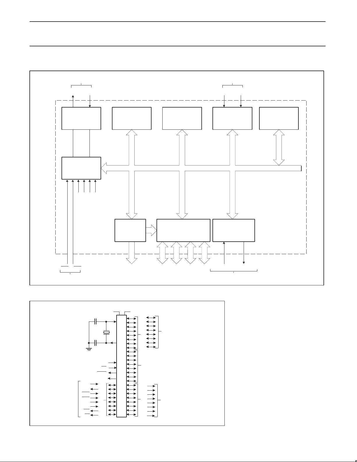
BLOCK DIAGRAM
FREQUENCY
REFERENCE
XTAL2 XTAL1
OSCILLATOR
AND
TIMING
CPU
INTERNAL
INTERRUPTS
PROGRAM
MEMORY
(4K x 8 ROM)
DATA
MEMORY
(128 x 8 RAM)
COUNTERS
T0 T1
TWO 16-BIT
TIMER/EVENT
COUNTERS
80C851/83C851
EEPROM
(256 x 8)
INT0
EXTERNAL
INTERRUPTS
LOGIC SYMBOL
INT1
RxD
TxD
INT0
INT1
T0
T1
WR
RD
SECONDARY FUNCTIONS
XTAL1
XTAL2
RST
EA
PSEN
ALE
PORT 3
64K BYTE BUS
EXPANSION
CONTRTOL
CONTROL
V
DD
PROGRAMMABLE I/O
PARALLEL PORTS,
ADDRESS/DATA BUS
AND I/O PINS
V
SS
ADDRESS AND
PORT 0
PORT 1PORT 2
DATA BUS
ADDRESS BUS
PROG SERIAL PORT
FULL DUPLEX UART
SYNCHRONOUS SHIFT
SERIAL IN SERIAL OUT
SHARED WITH
PORT 3
1998 Jul 03
3

Philips Semiconductors Product specification
CMOS single-chip 8-bit microcontroller
with on-chip EEPROM
PIN CONFIGURATIONS
P1.0
1
P1.1
2
P1.2
3
P1.3
4
P1.4
5
P1.5
6
P1.6
7
P1.7
8
RST
9
RxD/P3.0
TxD/P3.1
INT0/P3.2
/P3.3
INT1
T0/P3.4
T1/P3.5
WR
/P3.6
/P3.7
RD
XTAL2
XTAL1
V
7
17
SS
DUAL
10
IN-LINE
PACKAGE
11
12
13
14
15
16
17
18
19
20
6140
PLASTIC
LEADED
CHIP
CARRIER
40
39
38
37
36
35
34
33
32
31
30
29
28
27
26
25
24
23
22
21
V
DD
P0.0/AD0
P0.1/AD1
P0.2/AD2
P0.3/AD3
P0.4/AD4
P0.5/AD5
P0.6/AD6
P0.7/AD7
EA
ALE
PSEN
P2.7/A15
P2.6/A14
P2.5/A13
P2.4/A12
P2.3/A11
P2.2/A10
P2.1/A9
P2.0/A8
39
29
PLASTIC LEADED CHIP CARRIER PIN FUNCTIONS
7
17
Pin Function Pin Function
1 NC* 23 NC*
2 P1.0 24 P2.0/A8
3 P1.1 25 P2.1/A9
4 P1.2 26 P2.2/A10
5 P1.3 27 P2.3/A11
6 P1.4 28 P2.4/A12
7 P1.5 29 P2.5/A13
8 P1.6 30 P2.6/A14
9 P1.7 31 P2.7/A15
10 RST 32 PSEN
11 P3.0/RxD 33 ALE
12 NC* 34 NC*
13 P3.1/TxD 35 EA
14 P3.2/INT0 36 P0.7/AD7
15 P3.3/INT1 37 P0.6/AD6
16 P3.4/T0 38 P0.5/AD5
17 P3.5/T1 39 P0.4/AD4
18 P3.6/WR 40 P0.3/AD3
19 P3.7/RD 41 P0.2/AD2
20 XTAL2 42 P0.1/AD1
21 XTAL1 43 P0.0/AD0
22 V
SS
* NO INTERNAL CONNECTION
6140
PLCC
18 28
44 V
80C851/83C851
PLASTIC QUAD FLAT PACK PIN FUNCTIONS
44 34
39
29
DD
1
PQFP
11
12 22
Pin Function Pin Function
1 P1.5 23 P2.5/A13
2 P1.6 24 P2.6/A14
3 P1.7 25 P2.7/A15
4 RST 26 PSEN
5 P3.0/RxD 27 ALE
6 NC* 28 NC*
7 P3.1/TxD 29 EA
8 P3.2/INT0 30 P0.7/AD7
9 P3.3/INT1 31 P0.6/AD6
10 P3.4/T0 32 P0.5/AD5
11 P3.5/T1 33 P0.4/AD4
12 P3.6/WR 34 P0.3/AD3
13 P3.7RD 35 P0.2/AD2
14 XTAL2 36 P0.1/AD1
15 XTAL1 37 P0.0/AD0
16 V
SS
17 NC* 39 V
18 P2.0/A8 40 P1.0
19 P2.1/A9 41 P1.1
20 P2.2/A10 42 P1.2
21 P2.3/A11 43 P1.3
22 P2.4/A12 44 P1.4
* NO INTERNAL CONNECTION
38 V
33
23
DD
SS
1
11
1998 Jul 03
18 28
44
PLASTIC
QUAD
FLAT
PACK
12 22
34
33
23
4
Philips Semiconductors Product specification
CMOS single-chip 8-bit microcontroller
with on-chip EEPROM
PIN DESCRIPTION
PIN NO.
MNEMONIC DIP LCC QFP TYPE NAME AND FUNCTION
V
SS
V
DD
P0.0–0.7 39–32 43–36 37–30 I/O Port 0: Port 0 is an open-drain, bidirectional I/O port. Port 0 pins that have 1s written to
P1.0–P1.7 1–8 2–9 40–44,
P2.0–P2.7 21–28 24–31 18–25 I/O Port 2: Port 2 is an 8-bit bidirectional I/O port with internal pull-ups. Port 2 pins that have
P3.0–P3.7 10–17 11,
RST 9 10 4 I Reset: A high on this pin for two machine cycles while the oscillator is running, resets the
ALE 30 33 27 I/O Address Latch Enable: Output pulse for latching the low byte of the address during an
PSEN 29 32 26 O Program Store Enable: The read strobe to external program memory. When the device
EA 31 35 29 I External Access Enable: If during a RESET, EA is held at TTL, level HIGH, the CPU
XTAL1 19 21 15 I Crystal 1: Input to the inverting oscillator amplifier and input to the internal clock
XTAL2 18 20 14 O Crystal 2: Output from the inverting oscillator amplifier.
20 22 16, 39 I Ground: 0V reference.
40 44 38 I Power Supply: This is the power supply voltage for normal, idle, and power-down
1–3
13–195,7–13
10 11 5 I RxD (P3.0): Serial input port
11 13 7 O TxD (P3.1): Serial output port
12 14 8 I INT0 (P3.2): External interrupt
13 15 9 I INT1 (P3.3): External interrupt
14 16 10 I T0 (P3.4): Timer 0 external input
15 17 11 I T1 (P3.5): Timer 1 external input
16 18 12 O WR (P3.6): External data memory write strobe
17 19 13 O RD (P3.7): External data memory read strobe
operation.
them float and can be used as high-impedance inputs. Port 0 is also the multiplexed
low-order address and data bus during accesses to external program and data memory.
In this application, it uses strong internal pull-ups when emitting 1s.
I/O Port 1: Port 1 is an 8-bit bidirectional I/O port with internal pull-ups. Port 1 pins that have
1s written to them are pulled high by the internal pull-ups and can be used as inputs. As
inputs, port 1 pins that are externally pulled low will source current because of the
internal pull-ups. (See DC Electrical Characteristics: I
1s written to them are pulled high by the internal pull-ups and can be used as inputs. As
inputs, port 2 pins that are externally being pulled low will source current because of the
internal pull-ups. (See DC Electrical Characteristics: I
address byte during fetches from external program memory and during accesses to
external data memory that use 16-bit addresses (MOVX @DPTR). In this application, it
uses strong internal pull-ups when emitting 1s. During accesses to external data memory
that use 8-bit addresses (MOV @Ri), port 2 emits the contents of the P2 special function
register.
I/O Port 3: Port 3 is an 8-bit bidirectional I/O port with internal pull-ups. Port 3 pins that have
1s written to them are pulled high by the internal pull-ups and can be used as inputs. As
inputs, port 3 pins that are externally being pulled low will source current because of the
pull-ups. (See DC Electrical Characteristics: I
of the SC80C51 family, as listed below:
device. An internal diffused resistor to VSS permits a power-on reset using only an
external capacitor to V
access to external memory. In normal operation, ALE is emitted at a constant rate of 1/6
the oscillator frequency , and can be used for external timing or clocking. Note that one
ALE pulse is skipped during each access to external data memory.
is executing code from the external program memory, PSEN is activated twice each
machine cycle, except that two PSEN
external data memory. PSEN
memory.
executes out of the internal program memory ROM provided the Program Counter is less
than 4096. If during a RESET, EA
external program memory. EA
generator circuits.
.
DD
activations are skipped during each access to
is not activated during fetches from internal program
is held a TTL LOW level, the CPU executes out of
is not allowed to float.
). Port 3 also serves the special features
IL
80C851/83C851
).
IL
). Port 2 emits the high-order
IL
1998 Jul 03
5
Philips Semiconductors Product specification
CMOS single-chip 8-bit microcontroller
with on-chip EEPROM
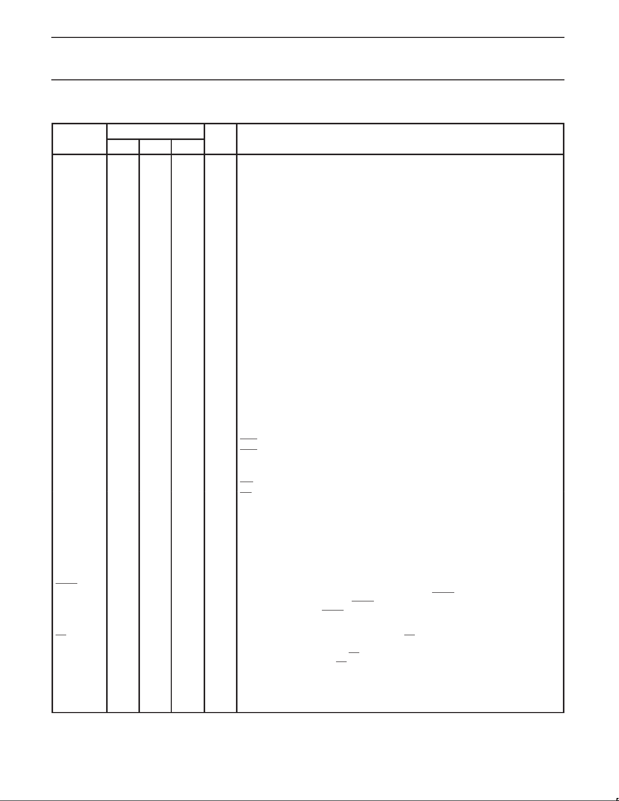
Table 1. 8XC851 Special Function Registers
SYMBOL DESCRIPTION
ACC* Accumulator E0H E7 E6 E5 E4 E3 E2 E1 E0 00H
B* B register F0H F7 F6 F5 F4 F3 F2 F1 F0 00H
DPTR:
DPH
DPL
EADRH# EEPROM addr
EADRL# EEPROM addr
ECNTRL# EEPROM control reg F6H IFE EEINT EWP – ECNTRL3ECNTRL2ECNTRL1ECNTRL000H
EDAT# EEPROM data
ETIM# EEPROM timer
IP* Interrupt priority B8H – – – PS PT1 PX1 PT0 PX0 xxx00000B
Data pointer
(2 bytes):
High byte
Low byte
reg-high
reg-low
register
register
DIRECT
ADDRESS
83H
82H
F3H 80H
F2H 00H
F4H xxH
F5H 08H
BIT ADDRESS, SYMBOL, OR ALTERNATIVE PORT FUNCTION
MSB LSB
EF EE ED EC EB EA E9 E8
BF BE BD BC BB BA B9 B8
80C851/83C851
RESET
VALUE
00H
00H
AF AE AD AC AB AA A9 A8
IE* Interrupt enable A8H EA – – ES ET1 EX1 ET0 EX0 0xx00000B
P0* Port 0 80H 87 86 85 84 83 82 81 80 FFH
P1* Port 1 90H 97 96 95 94 93 92 91 90 FFH
P2* Port 2 A0H A7 A6 A5 A4 A3 A2 A1 A0 FFH
P3* Port 3 B0H B7 B6 B5 B4 B3 B2 B1 B0 FFH
PCON Power control 87H SMOD – – – GF1 GF0 PD IDL 0xxx0000B
D7 D6 D5 D4 D3 D2 D1 D0
PSW* Program status word D0H CY AC F0 RS1 RS0 OV – P 00H
SBUF Serial data buffer 99H xxxxxxxxB
9F 9E 9D 9C 9B 9A 99 98
SCON* Serial port control 98H SM0 SM1 SM2 REN TB8 RB8 TI RI 00H
SP Stack pointer 81H 07H
8F 8E 8D 8C 8B 8A 89 88 00H
TCON* Timer/counter con-
trol
TMOD Timer/counter mode 89H GATE C/T M1 M0 GATE C/T M1 M0 00H
TH0 Timer 0 high byte 8CH 00H
TH1 Timer 1 high byte 8DH 00H
TL0 Timer 0 low byte 8AH 00H
TL1 Timer 1 low byte 8BH 00H
* SFRs are bit addressable.
# SFRs are modified from or added to the 80C51 SFRs.
88H TF1 TR1 TF0 TR0 IE1 IT1 IE0 IT0 00H
1998 Jul 03
6
Philips Semiconductors Product specification
CMOS single-chip 8-bit microcontroller
with on-chip EEPROM
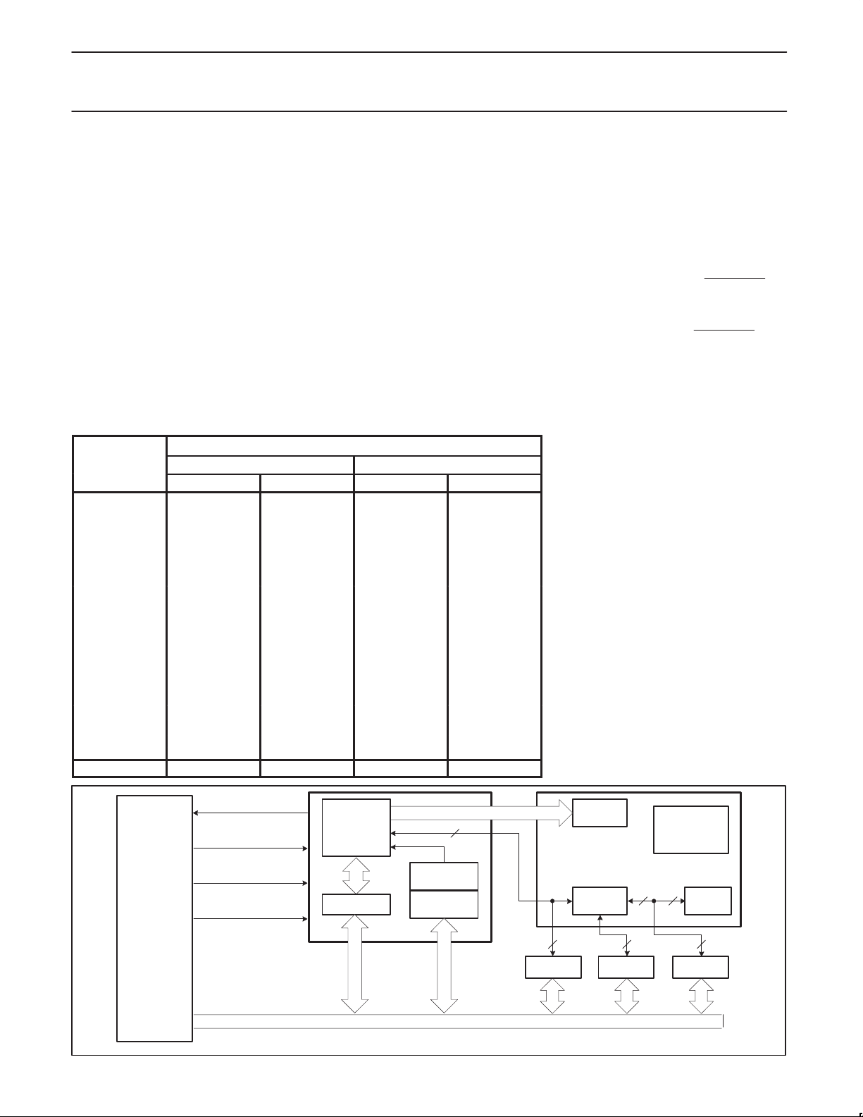
EEPROM
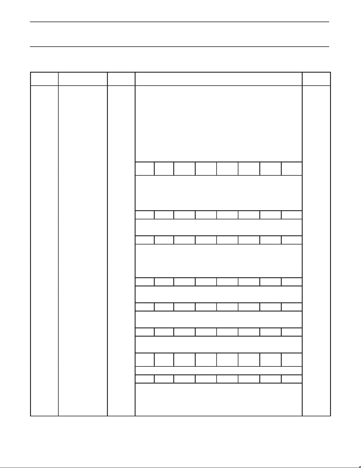
Communications between the CPU and the
EEPROM is accomplished via 5 special
function registers; 2 address registers (high
and low byte), 1 data register for read and
write operations, 1 control register, and 1
timer register to adapt the erase/write time to
the clock frequency. All registers can be read
and written. Figure 1 shows a block diagram
of the CPU, the EEPROM and the interface.
Register and Functional Description
Address Register (EADRH, EADRL)
The lower byte contains the address of one
of the 256 bytes. The higher byte (EADRH) is
for future extensions and for addressing the
security bits (see Security Facilities). The
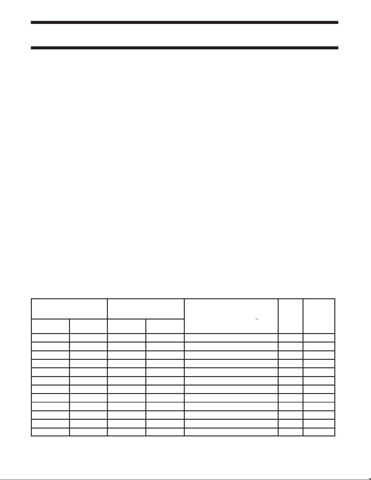
Table 2. Values for the Timer Register (ETIM)
f
XTAL1
1.0MHz – – 08 8
2.0MHz 02 2 13 19
3.0MHz 04 4 1D 29
4.0MHz 06 6 28 40
5.0MHz 08 8 32 50
6.0MHz 0A 10 3C 60
7.0MHz 0C 12 47 71
8.0MHz 0E 14 51 81
9.0MHz 10 16 5C 92
10.0MHz 12 18 66 102
11.0MHz 14 20 71 113
12.0MHz 16 22 7B 123
13.0MHz 18 24
14.0MHz 1A 26
15.0MHz 1C 28
16.0MHz 1E 30
.
.
24.0MHz 2C 4745
2ms WRITE TIME 10ms WRITE TIME
HEX DEC HEX DEC
EADRH register address is F3H. The EADRL
register address is F2H.
Data Register (EDAT)
This register is required for read and write
operations and also for row/block erase. In
write mode, its contents are written to the
addressed byte (for “row erase” and “block
erase” the contents are don’t care). The write
pulse starts all operations, except read. In
read mode, EDAT contains the data of the
addressed byte. The EDAT register address
is F4H.
Timer Register (ETIM)
The timer register is required to adapt the
erase/write time to the oscillator frequency.
The user has to ensure that the erase or
write (program) time is neither too short or
too long.
VALUES FOR ETIM
80C851/83C851
The ETIM register address is F5H. Table 2
contains the values which must be written to
the ETIM register by software for various
oscillator frequencies (the default value is
08H after RESET).
The general formula is:
2ms Write time:
f
Value (decimal,
to be rounded up)
10ms Write time:
f
Value (decimal)
Control Register (ECNTRL)
See Figure 2 for a description of this register.
The ECNTRL register address is F6H.
XTAL1
XTAL1
96
512
[kHz]
[kHz]
2
2
1998 Jul 03
CPU
INTERRUPT
POWER-DOWN IDLE
RESET
CLK
SEQUENCER
ECNTRL
8
CLOCK
GENERATOR
ETIM
INTERNAL BUS
Figure 1. EEPROM Interface Block Diagram
7
CONTROL
LOGIC
EEPROM
COLUMN
DECODER
88
EDATA EADRH EADRL
3
MATRIX
35
ROW
DECODER
 Loading...