

Philips 8XC52C32, 8XC54C32, 8XC58C32, 80C32, 8XC51FA User Manual
...
查询80C51FA供应商
INTEGRATED CIRCUITS
8XC52/54/58/80C32
8XC51FA/FB/FC/80C51FA
8XC51RA+/RB+/RC+/RD+/80C51RA +
80C51 8-bit microcontroller family
8K–64K/256–1K OTP/ROM/ROMless,
low voltage (2.7V–5.5V), low power , high speed (33 MHz)
Product specification
Supersedes data of 1998 Jun 04
IC20 Data Handbook
1999 Apr 01
Philips Semiconductors Product specification
80C51 8-bit microcontroller family
8K–64K/256–1K OTP/ROM/ROMless, low voltage (2.7V–5.5V),
low power, high speed (33 MHz)
DESCRIPTION
Three different Single-Chip 8-Bit Microcontroller families are
presented in this datasheet:
•80C32/8XC52/8XC54/8XC58
•80C51FA/8XC51FA/8XC51FB/8XC51FC
•80C51RA+/8XC51RA+/8XC51RB+/8XC51RC+/8XC51RD+
For applications requiring 4K ROM/EPROM, see the 8XC51/80C31
8-bit CMOS (low voltage, low power, and high speed)
microcontroller families datasheet.
All the families are Single-Chip 8-Bit Microcontrollers manufactured
in advanced CMOS process and are derivatives of the 80C51
microcontroller family. All the devices have the same instruction set
as the 80C51.
These devices provide architectural enhancements that make them
applicable in a variety of applications for general control systems.
ROM/EPROM
Memory Size
(X by 8)
80C31/8XC51
0K/4K 128 No No
80C32/8XC52/54/58
0K/8K/16K/32K 256 No No
80C51FA/8XC51FA/FB/FC
0K/8K/16K/32K 256 Yes No
80C51RA+/8XC51RA+/RB+/RC+
0K/8K/16K/32K 512 Yes Yes
8XC51RD+
64K 1024 Yes Yes
RAM Size
(X by 8)
Programmable
Timer Counter
(PCA)
Hardware
Watch Dog
Timer
FEA TURES
•80C51 Central Processing Unit
•Speed up to 33MHz
•Full static operation
•Operating voltage range: 2.7V to 5.5V @ 16MHz
•Security bits:
•Encryption array – 64 bytes
•RAM expandable to 64K bytes
•4 level priority interrupt
•6 or7 interrupt sources, depending on device
•Four 8-bit I/O ports
•Full-duplex enhanced UART
•Power control modes
•Programmable clock out
•Second DPTR register
•Asynchronous port reset
•Low EMI (inhibit ALE)
8XC52/54/58/80C32
8XC51FA/FB/FC/80C51FA
8XC51RA+/RB+/RC+/RD+/80C51RA+
– ROM – 2 bits
– OTP–EPROM – 3 bits
– Framing error detection
– Automatic address recognition
– Clock can be stopped and resumed
– Idle mode
– Power down mode
The ROMless devices, 80C32, 80C51FA, and 80C51RA+ can
address up to 64K of external memory. All the devices have four
8-bit I/O ports, three 16-bit timer/event counters, a multi-source,
four-priority-level, nested interrupt structure, an enhanced UART
and on-chip oscillator and timing circuits. For systems that require
extra memory capability up to 64k bytes, each can be expanded
using standard TTL-compatible memories and logic.
Its added features make it an even more powerful microcontroller for
applications that require pulse width modulation, high-speed I/O and
up/down counting capabilities such as motor control. It also has a
more versatile serial channel that facilitates multiprocessor
communications.
1999 Apr 01 853-2068 21142
2

Philips Semiconductors Product specification
80C51 8-bit microcontroller family
8K–64K/256–1K OTP/ROM/ROMless, low voltage (2.7V–5.5V),
low power, high speed (33 MHz)
BLOCK DIAGRAM
P0.0–P0.7 P2.0–P2.7
PORT 0
DRIVERS
V
CC
V
SS
RAM ADDR
REGISTER
B
REGISTER
RAM
ACC
TMP2
PORT 0
LATCH
TMP1
PORT 2
DRIVERS
PORT 2
LATCH
8XC52/54/58/80C32
8XC51FA/FB/FC/80C51FA
8XC51RA+/RB+/RC+/RD+/80C51RA+
ROM/EPROM
8
STACK
POINTER
PROGRAM
ADDRESS
REGISTER
PSEN
ALE/PROG
EAV
PP
RST
TIMING
AND
CONTROL
OSCILLATOR
XTAL1 XTAL2
INSTRUCTION
PD
REGISTER
PSW
PORT 1
LATCH
PORT 1
DRIVERS
P1.0–P1.7
ALU
SFRs
TIMERS
P.C.A. (FA & RA+ only)
PORT 3
LATCH
PORT 3
DRIVERS
P3.0–P3.7
BUFFER
PC
INCRE-
MENTER
8 16
PROGRAM
COUNTER
DPTR’S
MULTIPLE
SU00831B
1999 Apr 01
3
Philips Semiconductors Product specification
80C51 8-bit microcontroller family
8K–64K/256–1K OTP/ROM/ROMless, low voltage (2.7V–5.5V),
low power, high speed (33 MHz)
LOGIC SYMBOL
V
V
SS
CC
XTAL1
ADDRESS AND
DATA BUS
T2
T2EX
PORT 1PORT 2
ADDRESS BUS
SU00830
EA/V
PSEN
ALE/PROG
RxD
TxD
INT0
INT1
T0
T1
WR
RD
SECONDARY FUNCTIONS
XTAL2
RST
PP
PORT 0
PORT 3
PIN CONFIGURA TIONS
DUAL IN-LINE PACKAGE PIN FUNCTIONS
8XC52/54/58/80C32
8XC51FA/FB/FC/80C51FA
8XC51RA+/RB+/RC+/RD+/80C51RA+
PLASTIC LEADED CHIP CARRIER PIN FUNCTIONS
6140
7
17
Pin Function
1 NIC*
2 P1.0/T2
3 P1.1/T2EX
4 P1.2/ECI
5 P1.3/CEX0
6 P1.4/CEX1
7 P1.5/CEX2
8 P1.6/CEX3
9 P1.7/CEX4
10 RST
11 P3.0/RxD
12 NIC*
13 P3.1/TxD
14 P3.2/INT0
15 P3.3/INT1
* NO INTERNAL CONNECTION
LCC
18 28
Pin Function
16 P3.4/T0
17 P3.5/T1
18 P3.6/WR
19 P3.7/RD
20 XTAL2
21 XTAL1
22 V
SS
23 NIC*
24 P2.0/A8
25 P2.1/A9
26 P2.2/A10
27 P2.3/A11
28 P2.4/A12
29 P2.5/A13
30 P2.6/A14
39
29
Pin Function
31 P2.7/A15
32 PSEN
33 ALE/PROG
34 NIC*
35 EA/V
36 P0.7/AD7
37 P0.6/AD6
38 P0.5/AD5
39 P0.4/AD4
40 P0.3/AD3
41 P0.2/AD2
42 P0.1/AD1
43 P0.0/AD0
44 V
PP
CC
SU00023
T2/P1.0
T2EX/P1.1
ECI/P1.2
CEX0/P1.3
CEX1/P1.4
CEX2/P1.5
CEX3/P1.6
CEX4/P1.7
RST
RxD/P3.0
TxD/P3.1
/P3.2
INT0
INT1
/P3.3
T0/P3.4
T1/P3.5
/P3.6
WR
/P3.7
RD
XTAL2
XTAL1
V
V
1
2
3
4
5
6
7
8
9
DUAL
10
IN-LINE
PACKAGE
11
12
13
14
15
16
17
18
19
20
SS
40
P0.0/AD0
39
38
P0.1/AD1
37
P0.2/AD2
36
P0.3/AD3
35
P0.4/AD4
34
P0.5/AD5
33
P0.6/AD6
32
P0.7/AD7
EA/V
31
30
ALE/PROG
29
PSEN
28
P2.7/A15
27
P2.6/A14
26
P2.5/A13
25
P2.4/A12
24
P2.3/A11
23
P2.2/A10
22
P2.1/A9
21
P2.0/A8
CC
PP
SU00021
PLASTIC QUAD FLAT PACK
PIN FUNCTIONS
44 34
1
PQFP
11
12 22
Pin Function
1 P1.5/CEX2
2 P1.6/CEX3
3 P1.7/CEX4
4 RST
5 P3.0/RxD
6 NIC*
7 P3.1/TxD
8 P3.2/INT0
9 P3.3/INT1
10 P3.4/T0
11 P3.5/T1
12 P3.6/WR
13 P3.7/RD
14 XTAL2
15 XTAL1
* NO INTERNAL CONNECTION
Pin Function
16 V
SS
17 NIC*
18 P2.0/A8
19 P2.1/A9
20 P2.2/A10
21 P2.3/A11
22 P2.4/A12
23 P2.5/A13
24 P2.6/A14
25 P2.7/A15
26 PSEN
27 ALE/PROG
28 NIC*
29 EA
/V
30 P0.7/AD7
PP
33
23
Pin Function
31 P0.6/AD6
32 P0.5/AD5
33 P0.4/AD4
34 P0.3/AD3
35 P0.2/AD2
36 P0.1/AD1
37 P0.0/AD0
38 V
CC
39 NIC*
40 P1.0/T2
41 P1.1/T2EX
42 P1.2/ECI
43 P1.3/CEX0
44 P1.4/CEX1
SU00024
1999 Apr 01
4
Philips Semiconductors Product specification
80C51 8-bit microcontroller family
8K–64K/256–1K OTP/ROM/ROMless, low voltage (2.7V–5.5V),
low power, high speed (33 MHz)
8XC51RA+/RB+/RC+/RD+/80C51RA+
8XC52/54/58/80C32
8XC51FA/FB/FC/80C51FA
PIN DESCRIPTIONS
PIN NUMBER
MNEMONIC DIP LCC QFP TYPE NAME AND FUNCTION
V
SS
V
CC
P0.0–0.7 39–32 43–36 37–30 I/O Port 0: Port 0 is an open-drain, bidirectional I/O port. Port 0 pins that have 1s written to
P1.0–P1.7 1–8 2–9 40–44,
P2.0–P2.7 21–28 24–31 18–25 I/O Port 2: Port 2 is an 8-bit bidirectional I/O port with internal pull-ups. Port 2 pins that have 1s
P3.0–P3.7 10–17 11,
RST 9 10 4 I Reset: A high on this pin for two machine cycles while the oscillator is running, resets the
ALE/PROG 30 33 27 O Address Latch Enable/Program Pulse: Output pulse for latching the low byte of the
20 22 16 I Ground: 0V reference.
40 44 38 I Power Supply: This is the power supply voltage for normal, idle, and power-down operation.
them float and can be used as high-impedance inputs. Port 0 is also the multiplexed
low-order address and data bus during accesses to external program and data memory. In
this application, it uses strong internal pull-ups when emitting 1s. Port 0 also outputs the
code bytes during program verification and received code bytes during EPROM
programming. External pull-ups are required during program verification.
I/O Port 1: Port 1 is an 8-bit bidirectional I/O port with internal pull-ups. Port 1 pins that have 1s
1–3
1 2 40 I/O T2 (P1.0): Timer/Counter 2 external count input/Clockout (see Programmable Clock-Out)
2 3 41 I T2EX (P1.1): Timer/Counter 2 Reload/Capture/Direction Control
3 4 42 I ECI (P1.2): External Clock Input to the PCA
4 5 43 I/O CEX0 (P1.3): Capture/Compare External I/O for PCA module 0
5 6 44 I/O CEX1 (P1.4): Capture/Compare External I/O for PCA module 1
6 7 1 I/O CEX2 (P1.5): Capture/Compare External I/O for PCA module 2
7 8 2 I/O CEX3 (P1.6): Capture/Compare External I/O for PCA module 3
8 9 3 I/O CEX4 (P1.7): Capture/Compare External I/O for PCA module 4
13–195,7–13
10 11 5 I RxD (P3.0): Serial input port
11 13 7 O TxD (P3.1): Serial output port
12 14 8 I INT0 (P3.2): External interrupt
13 15 9 I INT1 (P3.3): External interrupt
14 16 10 I T0 (P3.4): Timer 0 external input
15 17 11 I T1 (P3.5): Timer 1 external input
16 18 12 O WR (P3.6): External data memory write strobe
17 19 13 O RD (P3.7): External data memory read strobe
written to them are pulled high by the internal pull-ups and can be used as inputs. As inputs,
port 1 pins that are externally pulled low will source current because of the internal pull-ups.
(See DC Electrical Characteristics: I
during program memory verification.
Alternate functions for 8XC51FX and 8XC51RX+ Port 1 include:
written to them are pulled high by the internal pull-ups and can be used as inputs. As inputs,
port 2 pins that are externally being pulled low will source current because of the internal
pull-ups. (See DC Electrical Characteristics: I
during fetches from external program memory and during accesses to external data memory
that use 16-bit addresses (MOVX @DPTR). In this application, it uses strong internal
pull-ups when emitting 1s. During accesses to external data memory that use 8-bit addresses
(MOV @Ri), port 2 emits the contents of the P2 special function register. Some Port 2 pins
receive the high order address bits during EPROM programming and verification.
I/O Port 3: Port 3 is an 8-bit bidirectional I/O port with internal pull-ups. Port 3 pins that have 1s
written to them are pulled high by the internal pull-ups and can be used as inputs. As inputs,
port 3 pins that are externally being pulled low will source current because of the pull-ups.
(See DC Electrical Characteristics: I
family, as listed below:
device. An internal diffused resistor to V
capacitor to V
address during an access to external memory. In normal operation, ALE is emitted at a
constant rate of 1/6 the oscillator frequency, and can be used for external timing or clocking.
Note that one ALE pulse is skipped during each access to external data memory. This pin is
also the program pulse input (PROG
setting SFR auxiliary.0. With this bit set, ALE will be active only during a MOVX instruction.
CC
.
). Port 1 also receives the low-order address byte
IL
). Port 2 emits the high-order address byte
IL
). Port 3 also serves the special features of the 80C51
IL
permits a power-on reset using only an external
SS
) during EPROM programming. ALE can be disabled by
1999 Apr 01
5

Philips Semiconductors Product specification
80C51 8-bit microcontroller family
8K–64K/256–1K OTP/ROM/ROMless, low voltage (2.7V–5.5V),
low power, high speed (33 MHz)
8XC51RA+/RB+/RC+/RD+/80C51RA+
8XC52/54/58/80C32
8XC51FA/FB/FC/80C51FA
PIN DESCRIPTIONS (Continued)
PIN NUMBER
MNEMONIC DIP LCC QFP TYPE NAME AND FUNCTION
PSEN 29 32 26 O Program Store Enable: The read strobe to external program memory. When executing
code from the external program memory, PSEN
except that two PSEN
PSEN
is not activated during fetches from internal program memory.
EA/V
PP
XTAL1 19 21 15 I Crystal 1: Input to the inverting oscillator amplifier and input to the internal clock generator
XTAL2 18 20 14 O Crystal 2: Output from the inverting oscillator amplifier.
NOTE:
To avoid “latch-up” effect at power-on, the voltage on any pin at any time must not be higher than V
31 35 29 I External Access Enable/Programming Supply Voltage: EA must be externally held low
to enable the device to fetch code from external program memory locations starting with
0000H. If EA
program counter contains an address greater than 8k Devices (IFFFH), 16k Devices
(3FFFH) or 32k Devices (7FFFH). Since the RD+ has 64k Internal Memory, the RD+ will
execute only from internal memory when EA
programming supply voltage (V
programmed, EA
circuits.
is held high, the device executes from internal program memory unless the
activations are skipped during each access to external data memory.
) during EPROM programming. If security bit 1 is
will be internally latched on Reset.
PP
is activated twice each machine cycle,
is held high. This pin also receives the 12.75V
+ 0.5V or VSS – 0.5V, respectively.
CC
1999 Apr 01
6

Philips Semiconductors Product specification
P80C32SBPN
0 to +70 Plastic DualIn line Package
27Vto55V
0to16
SOT129 1
P80C32SBPN
0
to
70
Plastic
D
al
In
line
Package
2
7V
to
5
5V
0
to
16
SOT129
1
P80C32SBAA
0 to +70 Plastic Leaded Chi
Carrier
27Vto55V
0to16
SOT187 2
P80C32SBAA
0
to
70
Plastic
Leaded
Chip
Carrier
2
7V
to
5
5V
0
to
16
SOT187
2
P80C32SBBB
0 to +70 Plastic Quad Flat Pack
27Vto55V
0to16
SOT307 2
P80C32SBBB
0
to
70
Plastic
Q
ad
Flat
Pack
2
7V
to
5
5V
0
to
16
SOT307
2
P80C32SFPN
40 to +85 Plastic Dual In line Package
27Vto55V
0to16
SOT129 1
P80C32SFPN
40
to
85
Plastic
D
al
In
line
Package
2
7V
to
5
5V
0
to
16
SOT129
1
P80C32SFAA
40 to +85 Plastic Leaded Chi
Carrier
27Vto55V
0to16
SOT187 2
P80C32SFAA
40
to
85
Plastic
Leaded
Chip
Carrier
2
7V
to
5
5V
0
to
16
SOT187
2
P80C32SFBB
40 to +85 Plastic Quad Flat Pack
27Vto55V
0to16
SOT307 2
P80C32SFBB
40
to
85
Plastic
Q
ad
Flat
Pack
2
7V
to
5
5V
0
to
16
SOT307
2
P80C32UBAA
0 to +70 Plastic Leaded Chi
Carrier
5V
0to33
SOT187 2
P80C32UBAA
0
to
70
Plastic
Leaded
Chip
Carrier
5V
0
to
33
SOT187
2
P80C32UBPN
0 to +70 Plastic Dual In line Package
5V
0to33
SOT129 1
P80C32UBPN
0
to
70
Plastic
D
al
In
line
Package
5V
0
to
33
SOT129
1
P80C32UBBB
0 to +70 Plastic Quad Flat Pack
5V
0to33
SOT307 2
P80C32UBBB
0
to
70
Plastic
Q
ad
Flat
Pack
5V
0
to
33
SOT307
2
P80C32UFAA
40 to +85 Plastic Leaded Chi
Carrier
5V
0to33
SOT187 2
P80C32UFAA
40
to
85
Plastic
Leaded
Chip
Carrier
5V
0
to
33
SOT187
2
P80C32UFPN
40 to +85 Plastic Dual In line Package
5V
0to33
SOT129 1
P80C32UFPN
40
to
85
Plastic
D
al
In
line
Package
5V
0
to
33
SOT129
1
P80C32UFBB
40 to +85 Plastic Quad Flat Pack
5V
0to33
SOT307 2
P80C32UFBB
40
to
85
Plastic
Q
ad
Flat
Pack
5V
0
to
33
SOT307
2
80C51 8-bit microcontroller family
8K–64K/256–1K OTP/ROM/ROMless, low voltage (2.7V–5.5V),
low power, high speed (33MHz)
-
-
-
-
-
-
-
-
-
-
#
DWG.
p
u
,
,
+
+
–
(MHz)
FREQ.
RANGE
VOLTAGE
AND PACKAGE
TEMPERATURE RANGE °C
.
.
.
.
.
.
.
p
u
,
,
+
+
.
.
-
u
u
,
,
+
+
–
.
.
.
p
,
+
–
p
u
,
+
–
u
,
,
+
+
8XC52/54/58/80C32
8XC51FA/FB/FC/80C51FA
8XC51RA+/RB+/RC+/RD+/80C51RA+
-
-
u
u
,
,
+
+
–
–
MEMORY SIZE
MEMORY SIZE
MEMORY SIZE
8XC52/54/58 AND 80C32 ORDERING INFORMATION
ROMless
32K × 8
16K × 8
8K × 8
ROM P80C52SBPN P80C54SBPN P80C58SBPN
OTP P87C52SBPN P87C54SBPN P87C58SBPN
OTP P87C52SBAA P87C54SBAA P87C58SBAA
OTP P87C52SBBB P87C54SBBB P87C58SBBB
OTP P87C52SFPN P87C54SFPN P87C58SFPN
OTP P87C52SFAA P87C54SFAA P87C58SFAA
OTP P87C52SFBB P87C54SFBB P87C58SFBB
OTP P87C52UBAA P87C54UBAA P87C58UBAA
OTP P87C52UBPN P87C54UBPN P87C58UBPN
OTP P87C52UBBB P87C54UBBB P87C58UBBB
OTP P87C52UFAA P87C54UFAA P87C58UFAA
OTP P87C52UFPN P87C54UFPN P87C58UFPN
ROM P80C52SBAA P80C54SBAA P80C58SBAA
ROM P80C52SBBB P80C54SBBB P80C58SBBB
ROM P80C52SFPN P80C54SFPN P80C58SFPN
ROM P80C52SFAA P80C54SFAA P80C58SFAA
ROM P80C52SFBB P80C54SFBB P80C58SFBB
ROM P80C52UBAA P80C54UBAA P80C58UBAA
ROM P80C52UBPN P80C54UBPN P80C58UBPN
ROM P80C52UBBB P80C54UBBB P80C58UBBB
ROM P80C52UFAA P80C54UFAA P80C58UFAA
ROM P80C52UFPN P80C54UFPN P80C58UFPN
71999 Apr 01
OTP P87C52UFBB P87C54UFBB P87C58UFBB
ROM P80C52UFBB P80C54UFBB P80C58UFBB
Note: For Multi Time Programmable devices, See P89C51RX+ Flash datasheet.

Philips Semiconductors Product specification
P80C51FA 4N
0 to +70 40 Pin Plastic Dual In line Pkg
27Vto55V
0to16
SOT129 1
P80C51FA
4N
0
to
70
40
Pin
Plastic
D
al
In
line
Pkg
2
7V
to
5
5V
0
to
16
SOT129
1
P80C51FA 4A
0 to +70 44 Pin Plastic Leaded Chi
Carrier
27Vto55V
0to16
SOT187 2
P80C51FA
4A
0
to
70
44
Pin
Plastic
Leaded
Chip
Carrier
2
7V
to
5
5V
0
to
16
SOT187
2
P80C51FA 4B
0 to +70 44 Pin Plastic Quad Flat Pack
27Vto55V
0to16
SOT307 2
P80C51FA
4B
0
to
70
44
Pin
Plastic
Q
ad
Flat
Pack
2
7V
to
5
5V
0
to
16
SOT307
2
P80C51FA 5N
40 to +85 40 Pin Plastic Dual In line Pkg
27Vto55V
0to16
SOT129 1
P80C51FA
5N
40
to
85
40
Pin
Plastic
D
al
In
line
Pkg
2
7V
to
5
5V
0
to
16
SOT129
1
P80C51FA 5A
40 to +85 44 Pin Plastic Leaded Chi
Carrier
27Vto55V
0to16
SOT187 2
P80C51FA
5A
40
to
85
44
Pin
Plastic
Leaded
Chip
Carrier
2
7V
to
5
5V
0
to
16
SOT187
2
P80C51FA 5B
40 to +85 44 Pin Plastic Quad Flat Pack
27Vto55V
0to16
SOT307 2
P80C51FA
5B
40
to
85
44
Pin
Plastic
Q
ad
Flat
Pack
2
7V
to
5
5V
0
to
16
SOT307
2
P80C51FA IN
0 to +70 40 Pin Plastic Dual In line Pkg
5V
0to33
SOT129 1
P80C51FA
IN
0
to
70
40
Pin
Plastic
D
al
In
line
Pkg
5V
0
to
33
SOT129
1
P80C51FA IA
0 to +70 44 Pin Plastic Leaded Chi
Carrier
5V
0to33
SOT187 2
P80C51FA
IA
0
to
70
44
Pin
Plastic
Leaded
Chip
Carrier
5V
0
to
33
SOT187
2
P80C51FA IB
0 to +70 44 Pin Plastic Quad Flat Pack
5V
0to33
SOT307 2
P80C51FA
IB
0
to
70
44
Pin
Plastic
Q
ad
Flat
Pack
5V
0
to
33
SOT307
2
P80C51FA JN
40 to +85 40 Pin Plastic Dual In line Pkg
5V
0to33
SOT129 1
P80C51FA
JN
40
to
85
40
Pin
Plastic
D
al
In
line
Pkg
5V
0
to
33
SOT129
1
P80C51FA JA
40 to +85 44 Pin Plastic Leaded Chi
Carrier
5V
0to33
SOT187 2
P80C51FA
JA
40
to
85
44
Pin
Plastic
Leaded
Chip
Carrier
5V
0
to
33
SOT187
2
P80C51FA JB
40 to +85 44 Pin Plastic Quad Flat Pack
5V
0to33
SOT307 2
P80C51FA
JB
40
to
85
44
Pin
Plastic
Q
ad
Flat
Pack
5V
0
to
33
SOT307
2
80C51 8-bit microcontroller family
8K–64K/256–1K OTP/ROM/ROMless, low voltage (2.7V–5.5V),
low power, high speed (33MHz)
-
-
-
-
-
-
-
-
-
-
#
DWG.
.
u
u
-
,
,
+
+
–
(MHz)
FREQ.
RANGE
VOLTAGE
AND PACKAGE
TEMPERATURE RANGE °C
.
.
.
.
.
.
.
.
p
u
-
-
,
,
+
+
.
.
.
u
u
-
,
,
+
+
–
.
.
.
.
p
u
-
,
,
+
+
–
–
p
u
-
-
,
,
+
+
8XC52/54/58/80C32
8XC51FA/FB/FC/80C51FA
8XC51RA+/RB+/RC+/RD+/80C51RA+
-
-
p
u
-
,
,
+
+
–
–
MEMORY SIZE
MEMORY SIZE
MEMORY SIZE
8XC51FA/FB/FC AND 80C51FA ORDERING INFORMATION
–
ROMless
32K × 8
16K × 8
8K × 8
ROM P83C51FA–4N P83C51FB–4N P83C51FC–4N
–
–
OTP P87C51FA–4N P87C51FB–4N P87C51FC–4N
OTP P87C51FA–4A P87C51FB–4A P87C51FC–4A
ROM P83C51FA–4A P83C51FB–4A P83C51FC–4A
ROM P83C51FA–4B P83C51FB–4B P83C51FC–4B
–
–
OTP P87C51FA–4B P87C51FB–4B P87C51FC–4B
OTP P87C51FA–5N P87C51FB–5N P87C51FC–5N
ROM P83C51FA–5N P83C51FB–5N P83C51FC–5N
ROM P83C51FA–5A P83C51FB–5A P83C51FC–5A
–
–
OTP P87C51FA–5A P87C51FB–5A P87C51FC–5A
OTP P87C51FA–5B P87C51FB–5B P87C51FC–5B
ROM P83C51FA–5B P83C51FB–5B P83C51FC–5B
ROM P83C51FA–IN P83C51FB–IN P83C51FC–IN
–
–
OTP P87C51FA–IN P87C51FB–IN P87C51FC–IN
OTP P87C51FA–IA P87C51FB–IA P87C51FC–IA
ROM P83C51FA–IA P83C51FB–IA P83C51FC–IA
ROM P83C51FA–IB P83C51FB–IB P83C51FC–IB
–
OTP P87C51FA–IB P87C51FB–IB P87C51FC–IB
OTP P87C51FA–JN P87C51FB–JN P87C51FC–JN
ROM P83C51FA–JN P83C51FB–JN P83C51FC–JN
81999 Apr 01
–
–
OTP P87C51FA–JA P87C51FB–JA P87C51FC–JA
ROM P83C51FA–JA P83C51FB–JA P83C51FC–JA
OTP P87C51FA–JB P87C51FB–JB P87C51FC–JB
ROM P83C51FA–JB P83C51FB–JB P83C51FC–JB
Note: For Multi Time Programmable devices, See P89C51RX+ Flash datasheet.

Philips Semiconductors Product specification
P80C51RA+4N
27Vto55V
0to16
SOT129 1
P80C51RA
4N
2
7V
to
5
5V
0
to
16
SOT129
1
P80C51RA+4A
27Vto55V
0to16
SOT187 2
P80C51RA
4A
2
7V
to
5
5V
0
to
16
SOT187
2
P80C51RA+4B
27Vto55V
0to16
SOT307 2
P80C51RA
4B
2
7V
to
5
5V
0
to
16
SOT307
2
P80C51RA+5N
27Vto55V
0to16
SOT129 1
P80C51RA
5N
2
7V
to
5
5V
0
to
16
SOT129
1
P80C51RA+5A
27Vto55V
0to16
SOT187 2
P80C51RA
5A
2
7V
to
5
5V
0
to
16
SOT187
2
P80C51RA+5B
27Vto55V
0to16
SOT307 2
P80C51RA
5B
2
7V
to
5
5V
0
to
16
SOT307
2
P80C51RA+IN
5V
0to33
SOT129 1
P80C51RA
IN
5V
0
to
33
SOT129
1
P80C51RA+IA
5V
0to33
SOT187 2
P80C51RA
IA
5V
0
to
33
SOT187
2
P80C51RA+IB
5V
0to33
SOT307 2
P80C51RA
IB
5V
0
to
33
SOT307
2
P80C51RA+JN
5V
0to33
SOT129 1
P80C51RA
JN
5V
0
to
33
SOT129
1
P80C51RA+JA
5V
0to33
SOT187 2
P80C51RA
JA
5V
0
to
33
SOT187
2
P80C51RA+JB
5V
0to33
SOT307-2
P80C51RA+JB
5V
0
to
33
SOT307
2
80C51 8-bit microcontroller family
8K–64K/256–1K OTP/ROM/ROMless, low voltage (2.7V–5.5V),
low power, high speed (33MHz)
#
DWG.
(MHz)
FREQ.
RANGE
VOLTAGE
AND PACKAGE
-
.
.
0 to +70,
-
.
.
0 to +70,
-
.
.
0 to +70,
-
.
.
–40 to +85,
–40 to +85,
-
.
.
-
.
.
–40 to +85,
0 to +70,
-
-
0 to +70,
-
0 to +70,
8XC52/54/58/80C32
8XC51FA/FB/FC/80C51FA
8XC51RA+/RB+/RC+/RD+/80C51RA+
-
–40 to +85,
-
–40 to +85,
–40 to +85,
-
TEMPERATURE RANGE °C
ROMless
64K × 8
MEMORY SIZE
32K × 8
MEMORY SIZE
16K × 8
MEMORY SIZE
40-Pin Plastic Dual In-line Pkg.
+
44-Pin Plastic Leaded Chip Carrier
+
44-Pin Plastic Quad Flat Pack
40-Pin Plastic Dual In-line Pkg.
+
+
44-Pin Plastic Leaded Chip Carrier
+
44-Pin Plastic Quad Flat Pack
+
40-Pin Plastic Dual In-line Pkg.
44-Pin Plastic Leaded Chip Carrier
+
+
44-Pin Plastic Quad Flat Pack
+
40-Pin Plastic Dual In-line Pkg.
+
44-Pin Plastic Leaded Chip Carrier
+
44-Pin Plastic Quad Flat Pack
MEMORY SIZE
87C51RA+/RB+/RC+/RD+ AND 80C51RA+ ORDERING INFORMATION
8K × 8
OTP P87C51RA+4N P87C51RB+4N P87C51RC+4N P87C51RD+4N
ROM P83C51RA+4N P83C51RB+4N P83C51RC+4N P83C51RD+4N
OTP P87C51RA+4A P87C51RB+4A P87C51RC+4A P87C51RD+4A
ROM P83C51RA+4A P83C51RB+4A P83C51RC+4A P83C51RD+4A
OTP P87C51RA+4B P87C51RB+4B P87C51RC+4B P87C51RD+4B
ROM P83C51RA+4B P83C51RB+4B P83C51RC+4B P83C51RD+4B
OTP P87C51RA+5N P87C51RB+5N P87C51RC+5N P87C51RD+5N
ROM P83C51RA+5N P83C51RB+5N P83C51RC+5N P83C51RD+5N
OTP P87C51RA+5A P87C51RB+5A P87C51RC+5A P87C51RD+5A
ROM P83C51RA+5A P83C51RB+5A P83C51RC+5A P83C51RD+5A
OTP P87C51RA+5B P87C51RB+5B P87C51RC+5B P87C51RD+5B
ROM P83C51RA+5B P83C51RB+5B P83C51RC+5B P83C51RD+5B
OTP P87C51RA+IN P87C51RB+IN P87C51RC+IN P87C51RD+IN
ROM P83C51RA+IN P83C51RB+IN P83C51RC+IN P83C51RD+IN
OTP P87C51RA+IA P87C51RB+IA P87C51RC+IA P87C51RD+IA
ROM P83C51RA+IA P83C51RB+IA P83C51RC+IA P83C51RD+IA
91999 Apr 01
OTP P87C51RA+IB P87C51RB+IB P87C51RC+IB P87C51RD+IB
ROM P83C51RA+IB P83C51RB+IB P83C51RC+IB P83C51RD+IB
ROM P83C51RA+JN P83C51RB+JN P83C51RC+JN P83C51RD+JN
OTP P87C51RA+JN P87C51RB+JN P87C51RC+JN P87C51RD+JN
OTP P87C51RA+JA P87C51RB+JA P87C51RC+JA P87C51RD+JA
ROM P83C51RA+JA P83C51RB+JA P83C51RC+JA P83C51RD+JA
ROM P83C51RA+JB P83C51RB+JB P83C51RC+JB P83C51RD+JB
OTP P87C51RA+JB P87C51RB+JB P87C51RC+JB P87C51RD+JB
Note: For Multi Time Programmable devices, See P89C51RX+ Flash datasheet.
Philips Semiconductors Product specification
80C51 8-bit microcontroller family
8K–64K/256–1K OTP/ROM/ROMless, low voltage (2.7V–5.5V),
low power, high speed (33MHz)
8XC51RA+/RB+/RC+/RD+/80C51RA+
8XC52/54/58/80C32
8XC51FA/FB/FC/80C51FA
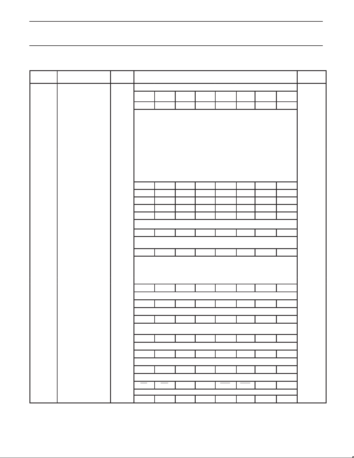
Table 1. 8XC52/54/58/80C32 Special Function Registers
SYMBOL DESCRIPTION
ACC* Accumulator E0H E7 E6 E5 E4 E3 E2 E1 E0 00H
AUXR# Auxiliary 8EH – – – – – – – AO xxxxxxx0B
AUXR1# Auxiliary 1 A2H – – – LPEP
B* B register F0H F7 F6 F5 F4 F3 F2 F1 F0 00H
DPTR: Data Pointer (2 bytes)
DPH Data Pointer High 83H 00H
DPL Data Pointer Low 82H 00H
IE* Interrupt Enable A8H EA – ET2 ES ET1 EX1 ET0 EX0 0x000000B
IP* Interrupt Priority B8H – – PT2 PS PT1 PX1 PT0 PX0 xx000000B
IPH# Interrupt Priority High B7H – – PT2H PSH PT1H PX1H PT0H PX0H xx000000B
P0* Port 0 80H AD7 AD6 AD5 AD4 AD3 AD2 AD1 AD0 FFH
P1* Port 1 90H – – – – – – T2EX T2 FFH
P2* Port 2 A0H AD15 AD14 AD13 AD12 AD11 AD10 AD9 AD8 FFH
P3* Port 3 B0H RD WR T1 T0 INT1 INT0 TxD RxD FFH
DIRECT
ADDRESS
BIT ADDRESS, SYMBOL, OR ALTERNATIVE PORT FUNCTION
MSB LSB
3
GF3 0 – DPS xxx0xxx0B
AF AE AD AC AB AA A9 A8
BF BE BD BC BB BA B9 B8
B7 B6 B5 B4 B3 B2 B1 B0
87 86 85 84 83 82 81 80
97 96 95 94 93 92 91 90
A7 A6 A5 A4 A3 A2 A1 A0
B7 B6 B5 B4 B3 B2 B1 B0
RESET
VALUE
1
PCON#
PSW* Program Status Word D0H CY AC F0 RS1 RS0 OV – P 000000x0B
RCAP2H# Timer 2 Capture High CBH 00H
RCAP2L# T imer 2 Capture Low CAH 00H
SADDR# Slave Address A9H 00H
SADEN# Slave Address Mask B9H 00H
SBUF Serial Data Buffer 99H xxxxxxxxB
SCON* Serial Control 98H
SP Stack Pointer 81H 07H
TCON* Timer Control 88H TF1 TR1 TF0 TR0 IE1 IT1 IE0 IT0 00H
T2CON* Timer 2 Control C8H TF2 EXF2 RCLK TCLK EXEN2 TR2 C/T2 CP/RL2 00H
T2MOD# Timer 2 Mode Control C9H – – – – – – T2OE DCEN xxxxxx00B
TH0 Timer High 0 8CH 00H
TH1 Timer High 1 8DH 00H
TH2# Timer High 2 CDH 00H
TL0 Timer Low 0 8AH 00H
TL1 Timer Low 1 8BH 00H
TL2# Timer Low 2 CCH 00H
TMOD Timer Mode 89H GATE C/T M1 M0 GATE C/T M1 M0 00H
* SFRs are bit addressable.
# SFRs are modified from or added to the 80C51 SFRs.
– Reserved bits.
1. Reset value depends on reset source.
2. Bit will not be affected by Reset.
3. LPEP – Low Power OTP–EPROM only operation.
Power Control 87H SMOD1 SMOD0 – POF
D7 D6 D5 D4 D3 D2 D1 D0
9F 9E 9D 9C 9B 9A 99 98
SM0/FE
8F 8E 8D 8C 8B 8A 89 88
CF CE CD CC CB CA C9 C8
SM1 SM2 REN TB8 RB8 TI RI 00H
2
GF1 GF0 PD IDL 00xx0000B
1999 Apr 01
10
Philips Semiconductors Product specification
80C51 8-bit microcontroller family
8K–64K/256–1K OTP/ROM/ROMless, low voltage (2.7V–5.5V),
low power, high speed (33MHz)
8XC51RA+/RB+/RC+/RD+/80C51RA+
8XC52/54/58/80C32
8XC51FA/FB/FC/80C51FA
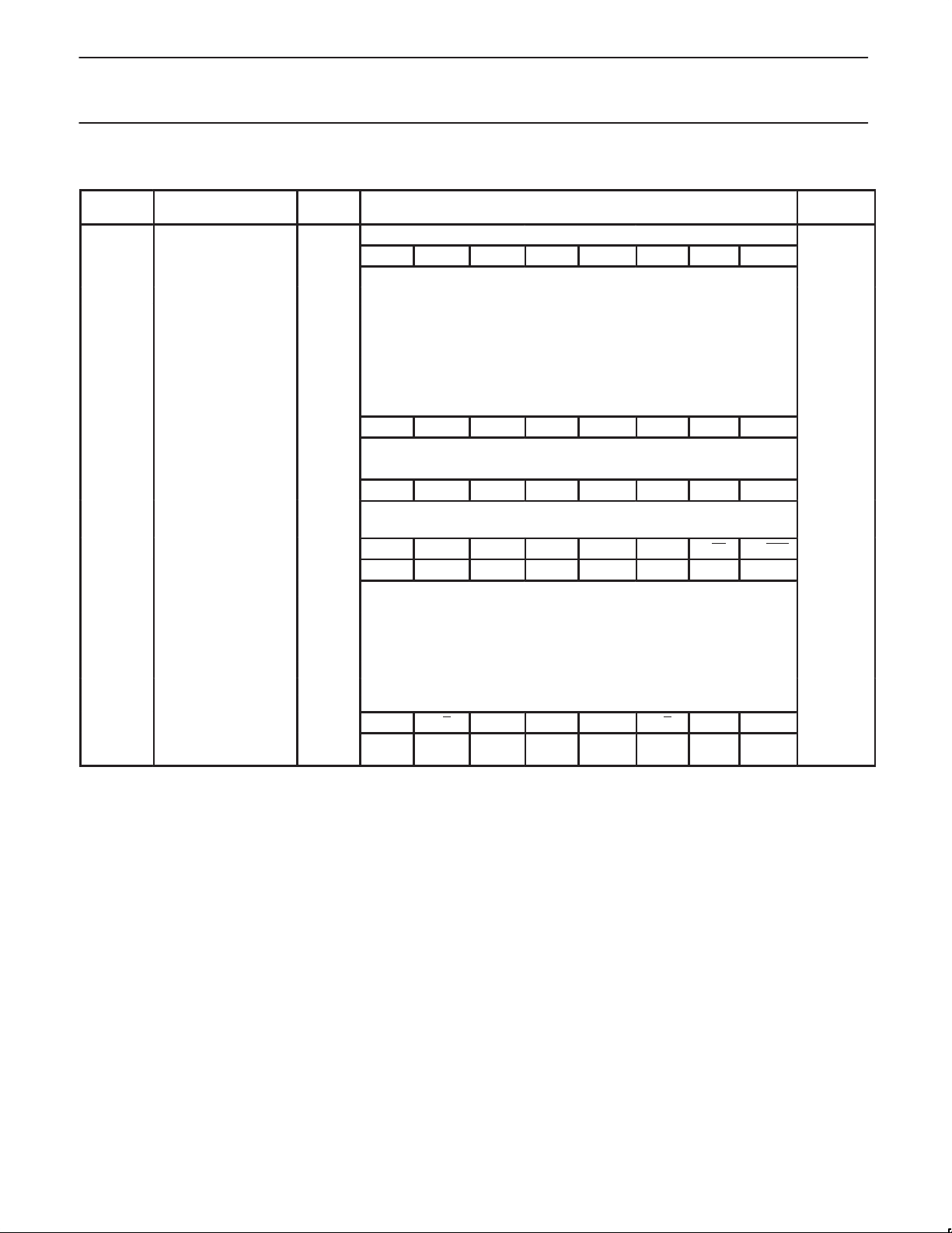
T able 2. 8XC51FA/FB/FC, 8XC51RA+/RB+/RC+/RD+ Special Function Registers
SYMBOL DESCRIPTION
ACC* Accumulator E0H E7 E6 E5 E4 E3 E2 E1 E0 00H
AUXR# Auxiliary 8EH – – – – – –
AUXR1# Auxiliary 1 A2H – – – LPEP3GF3 0 – DPS xxx0xxx0B
B* B register F0H F7 F6 F5 F4 F3 F2 F1 F0 00H
CCAP0H# Module 0 Capture High FAH xxxxxxxxB
CCAP1H# Module 1 Capture High FBH xxxxxxxxB
CCAP2H# Module 2 Capture High FCH xxxxxxxxB
CCAP3H# Module 3 Capture High FDH xxxxxxxxB
CCAP4H# Module 4 Capture High FEH xxxxxxxxB
CCAP0L# Module 0 Capture Low EAH xxxxxxxxB
CCAP1L# Module 1 Capture Low EBH xxxxxxxxB
CCAP2L# Module 2 Capture Low ECH xxxxxxxxB
CCAP3L# Module 3 Capture Low EDH xxxxxxxxB
CCAP4L# Module 4 Capture Low EEH xxxxxxxxB
CCAPM0# Module 0 Mode DAH – ECOM CAPP CAPN MAT TOG PWM ECCF x0000000B
CCAPM1# Module 1 Mode DBH – ECOM CAPP CAPN MAT TOG PWM ECCF x0000000B
CCAPM2# Module 2 Mode DCH – ECOM CAPP CAPN MAT TOG PWM ECCF x0000000B
CCAPM3# Module 3 Mode DDH – ECOM CAPP CAPN MAT TOG PWM ECCF x0000000B
CCAPM4# Module 4 Mode DEH – ECOM CAPP CAPN MAT TOG PWM ECCF x0000000B
CCON*# PCA Counter Control D8H CF CR – CCF4 CCF3 CCF2 CCF1 CCF0 00x00000B
CH# PCA Counter High F9H 00H
CL# PCA Counter Low E9H 00H
CMOD# PCA Counter Mode D9H CIDL WDTE – – – CPS1 CPS0 ECF 00xxx000B
DPTR: Data Pointer (2 bytes)
DPH Data Pointer High 83H 00H
DPL Data Pointer Low 82H 00H
IE* Interrupt Enable A8H EA EC ET2 ES ET1 EX1 ET0 EX0 00H
IP* Interrupt Priority B8H – PPC PT2 PS PT1 PX1 PT0 PX0 x0000000B
IPH# Interrupt Priority High B7H – PPCH PT2H PSH PT1H PX1H PT0H PX0H x0000000B
DIRECT
ADDRESS
BIT ADDRESS, SYMBOL, OR ALTERNATIVE PORT FUNCTION
MSB LSB
EXTRAM
(RX+ only)
DF DE DD DC DB DA D9 D8
AF AE AD AC AB AA A9 A8
BF BE BD BC BB BA B9 B8
B7 B6 B5 B4 B3 B2 B1 B0
AO xxxxxx00B
RESET
VALUE
87 86 85 84 83 82 81 80
P0* Port 0 80H AD7 AD6 AD5 AD4 AD3 AD2 AD1 AD0 FFH
97 96 95 94 93 92 91 90
P1* Port 1 90H CEX4 CEX3 CEX2 CEX1 CEX0 ECI T2EX T2 FFH
A7 A6 A5 A4 A3 A2 A1 A0
P2* Port 2 A0H AD15 AD14 AD13 AD12 AD11 AD10 AD9 AD8 FFH
B7 B6 B5 B4 B3 B2 B1 B0
P3* Port 3 B0H RD WR T1 T0 INT1 INT0 TxD RxD FFH
1
PCON#
* SFRs are bit addressable.
# SFRs are modified from or added to the 80C51 SFRs.
– Reserved bits.
1. Reset value depends on reset source.
2. Bit will not be affected by Reset.
3. LPEP – Low Power OTP–EPROM only operation.
1999 Apr 01
Power Control 87H SMOD1 SMOD0 – POF
11
2
GF1 GF0 PD IDL 00xx0000B
Philips Semiconductors Product specification
80C51 8-bit microcontroller family
8K–64K/256–1K OTP/ROM/ROMless, low voltage (2.7V–5.5V),
low power, high speed (33MHz)
8XC51RA+/RB+/RC+/RD+/80C51RA+
8XC52/54/58/80C32
8XC51FA/FB/FC/80C51FA
Table 2. 8XC51FA/FB/FC, 8XC51RA+/RB+/RC+/RD+ Special Function Registers (Continued)
SYMBOL DESCRIPTION
PSW* Program Status Word D0H CY AC F0 RS1 RS0 OV – P 000000x0B
RACAP2H# Timer 2 Capture High CBH 00H
RACAP2L# Timer 2 Capture Low CAH 00H
SADDR# Slave Address A9H 00H
SADEN# Slave Address Mask B9H 00H
SBUF Serial Data Buffer 99H xxxxxxxxB
SCON* Serial Control 98H
SP Stack Pointer 81H 07H
TCON* Timer Control 88H TF1 TR1 TF0 TR0 IE1 IT1 IE0 IT0 00H
DIRECT
ADDRESS
BIT ADDRESS, SYMBOL, OR ALTERNATIVE PORT FUNCTION
MSB LSB
D7 D6 D5 D4 D3 D2 D1 D0
9F 9E 9D 9C 9B 9A 99 98
SM0/FE
8F 8E 8D 8C 8B 8A 89 88
SM1 SM2 REN TB8 RB8 TI RI 00H
RESET
VALUE
CF CE CD CC CB CA C9 C8
T2CON* Timer 2 Control C8H TF2 EXF2 RCLK TCLK EXEN2 TR2 C/T2 CP/RL2 00H
T2MOD# Timer 2 Mode Control C9H – – – – – – T2OE DCEN xxxxxx00B
TH0 Timer High 0 8CH 00H
TH1 Timer High 1 8DH 00H
TH2# Timer High 2 CDH 00H
TL0 Timer Low 0 8AH 00H
TL1 Timer Low 1 8BH 00H
TL2# Timer Low 2 CCH 00H
TMOD Timer Mode 89H GATE C/T M1 M0 GATE C/T M1 M0 00H
WDTRST HDW Watchdog
Timer Reset (RX+ only)
* SFRs are bit addressable.
# SFRs are modified from or added to the 80C51 SFRs.
– Reserved bits.
OSCILLA T OR CHARACTERISTICS
XTAL1 and XTAL2 are the input and output, respectively, of an
inverting amplifier . The pins can be configured for use as an on-chip
oscillator.
To drive the device from an external clock source, XTAL1 should be
driven while XTAL2 is left unconnected. There are no requirements
on the duty cycle of the external clock signal, because the input to
the internal clock circuitry is through a divide-by-two flip-flop.
However, minimum and maximum high and low times specified in
the data sheet must be observed.
0A6H
RESET
A reset is accomplished by holding the RST pin high for at least two
machine cycles (24 oscillator periods), while the oscillator is running.
To insure a good power-on reset, the RST pin must be high long
enough to allow the oscillator time to start up (normally a few
milliseconds) plus two machine cycles. At power-on, the voltage on
V
and RST must come up at the same time for a proper start-up.
CC
Ports 1, 2, and 3 will asynchronously be driven to their reset
condition when a voltage above V
(min.) is applied to RESET.
IH1
1999 Apr 01
12

Philips Semiconductors Product specification
80C51 8-bit microcontroller family
8K–64K/256–1K OTP/ROM/ROMless, low voltage (2.7V–5.5V),
low power, high speed (33MHz)
LOW POWER MODES
Stop Clock Mode
The static design enables the clock speed to be reduced down to
0 MHz (stopped). When the oscillator is stopped, the RAM and
Special Function Registers retain their values. This mode allows
step-by-step utilization and permits reduced system power
consumption by lowering the clock frequency down to any value. For
lowest power consumption the Power Down mode is suggested.
Idle Mode
In the idle mode (see Table 3), the CPU puts itself to sleep while all
of the on-chip peripherals stay active. The instruction to invoke the
idle mode is the last instruction executed in the normal operating
mode before the idle mode is activated. The CPU contents, the
on-chip RAM, and all of the special function registers remain intact
during this mode. The idle mode can be terminated either by any
enabled interrupt (at which time the process is picked up at the
interrupt service routine and continued), or by a hardware reset
which starts the processor in the same manner as a power-on reset.
Power-Down Mode
To save even more power, a Power Down mode (see Table 3) can
be invoked by software. In this mode, the oscillator is stopped and
the instruction that invoked Power Down is the last instruction
executed. The on-chip RAM and Special Function Registers retain
their values down to 2.0V and care must be taken to return V
the minimum specified operating voltages before the Power Down
Mode is terminated.
Either a hardware reset or external interrupt can be used to exit from
Power Down. Reset redefines all the SFRs but does not change the
on-chip RAM. An external interrupt allows both the SFRs and the
on-chip RAM to retain their values.
To properly terminate Power Down the reset or external interrupt
should not be executed before V
operating level and must be held active long enough for the
oscillator to restart and stabilize (normally less than 10ms).
With an external interrupt, INT0 and INT1 must be enabled and
configured as level-sensitive. Holding the pin low restarts the oscillator
but bringing the pin back high completes the exit. Once the interrupt
is serviced, the next instruction to be executed after RETI will be the
one following the instruction that put the device into Power Down.
is restored to its normal
CC
CC
to
LPEP
The LPEP bit (AUXR.4), only needs to be set for applications
operating at V
less than 4V.
CC
8XC52/54/58/80C32
8XC51FA/FB/FC/80C51FA
8XC51RA+/RB+/RC+/RD+/80C51RA+
POWER OFF FLAG
The Power Off Flag (POF) is set by on-chip circuitry when the V
level on the 8XC51FX/8XC51RX+ rises from 0 to 5V . The POF bit
can be set or cleared by software allowing a user to determine if the
reset is the result of a power-on or a warm start after powerdown.
The V
unaffected by the V
level must remain above 3V for the POF to remain
CC
CC
level.
CC
Design Consideration
•When the idle mode is terminated by a hardware reset, the device
normally resumes program execution, from where it left off, up to
two machine cycles before the internal reset algorithm takes
control. On-chip hardware inhibits access to internal RAM in this
event, but access to the port pins is not inhibited. To eliminate the
possibility of an unexpected write when Idle is terminated by reset,
the instruction following the one that invokes Idle should not be
one that writes to a port pin or to external memory.
ONCE Mode
The ONCE (“On-Circuit Emulation”) Mode facilitates testing and
debugging of systems without the device having to be removed from
the circuit. The ONCE Mode is invoked by:
1. Pull ALE low while the device is in reset and PSEN
2. Hold ALE low as RST is deactivated.
While the device is in ONCE Mode, the Port 0 pins go into a float
state, and the other port pins and ALE and PSEN
high. The oscillator circuit remains active. While the device is in this
mode, an emulator or test CPU can be used to drive the circuit.
Normal operation is restored when a normal reset is applied.
Programmable Clock-Out
A 50% duty cycle clock can be programmed to come out on P1.0.
This pin, besides being a regular I/O pin, has two alternate
functions. It can be programmed:
1. to input the external clock for Timer/Counter 2, or
2. to output a 50% duty cycle clock ranging from 61Hz to 4MHz at a
16MHz operating frequency.
To configure the Timer/Counter 2 as a clock generator, bit C/T
T2CON) must be cleared and bit T20E in T2MOD must be set. Bit
TR2 (T2CON.2) also must be set to start the timer.
The Clock-Out frequency depends on the oscillator frequency and
the reload value of Timer 2 capture registers (RCAP2H, RCAP2L)
as shown in this equation:
Oscillator Frequency
4 (65536 RCAP2H, RCAP2L)
Where (RCAP2H,RCAP2L) = the content of RCAP2H and RCAP2L
taken as a 16-bit unsigned integer.
In the Clock-Out mode Timer 2 roll-overs will not generate an
interrupt. This is similar to when it is used as a baud-rate generator.
It is possible to use Timer 2 as a baud-rate generator and a clock
generator simultaneously. Note, however, that the baud-rate and the
Clock-Out frequency will be the same.
is high;
are weakly pulled
2 (in
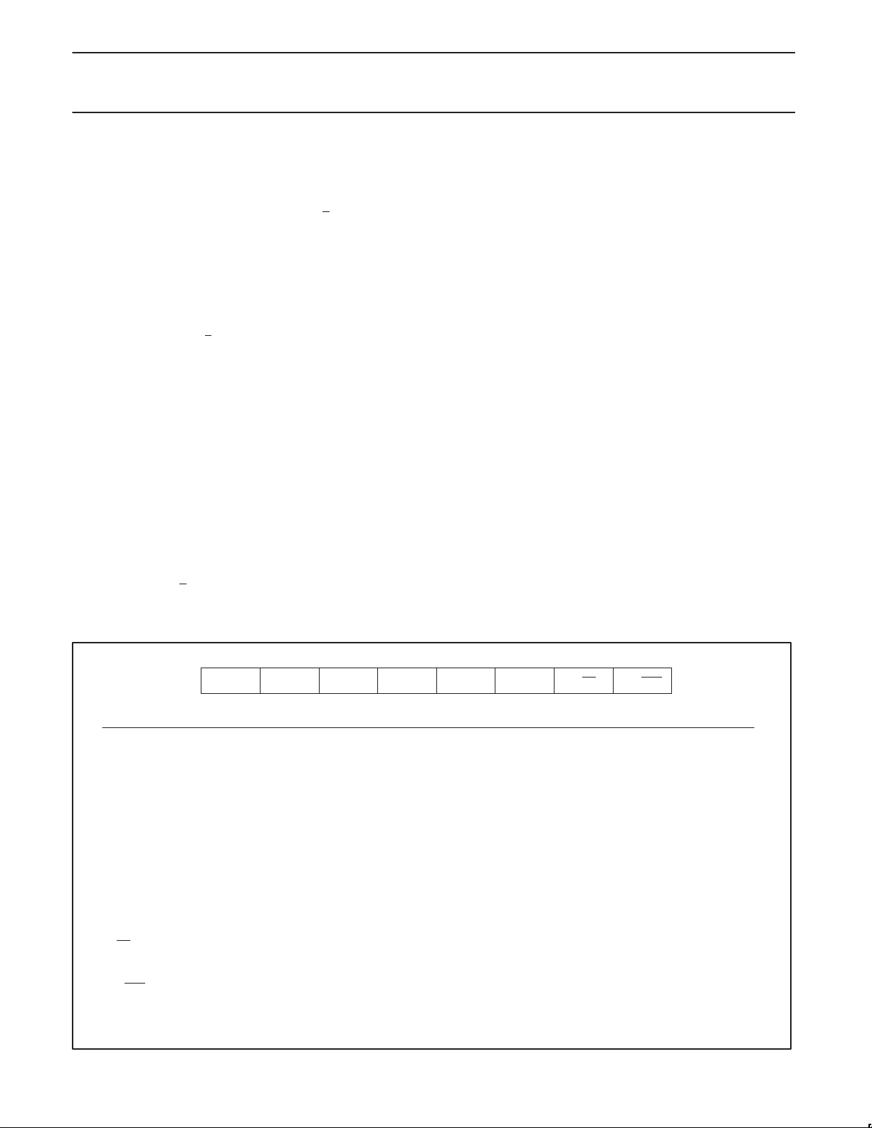
Table 3. External Pin Status During Idle and Power-Down Mode
MODE PROGRAM MEMORY ALE PSEN PORT 0 PORT 1 PORT 2 PORT 3
Idle Internal 1 1 Data Data Data Data
Idle External 1 1 Float Data Address Data
Power-down Internal 0 0 Data Data Data Data
Power-down External 0 0 Float Data Data Data
1999 Apr 01
13
Philips Semiconductors Product specification
80C51 8-bit microcontroller family
8K–64K/256–1K OTP/ROM/ROMless, low voltage (2.7V–5.5V),
low power, high speed (33MHz)
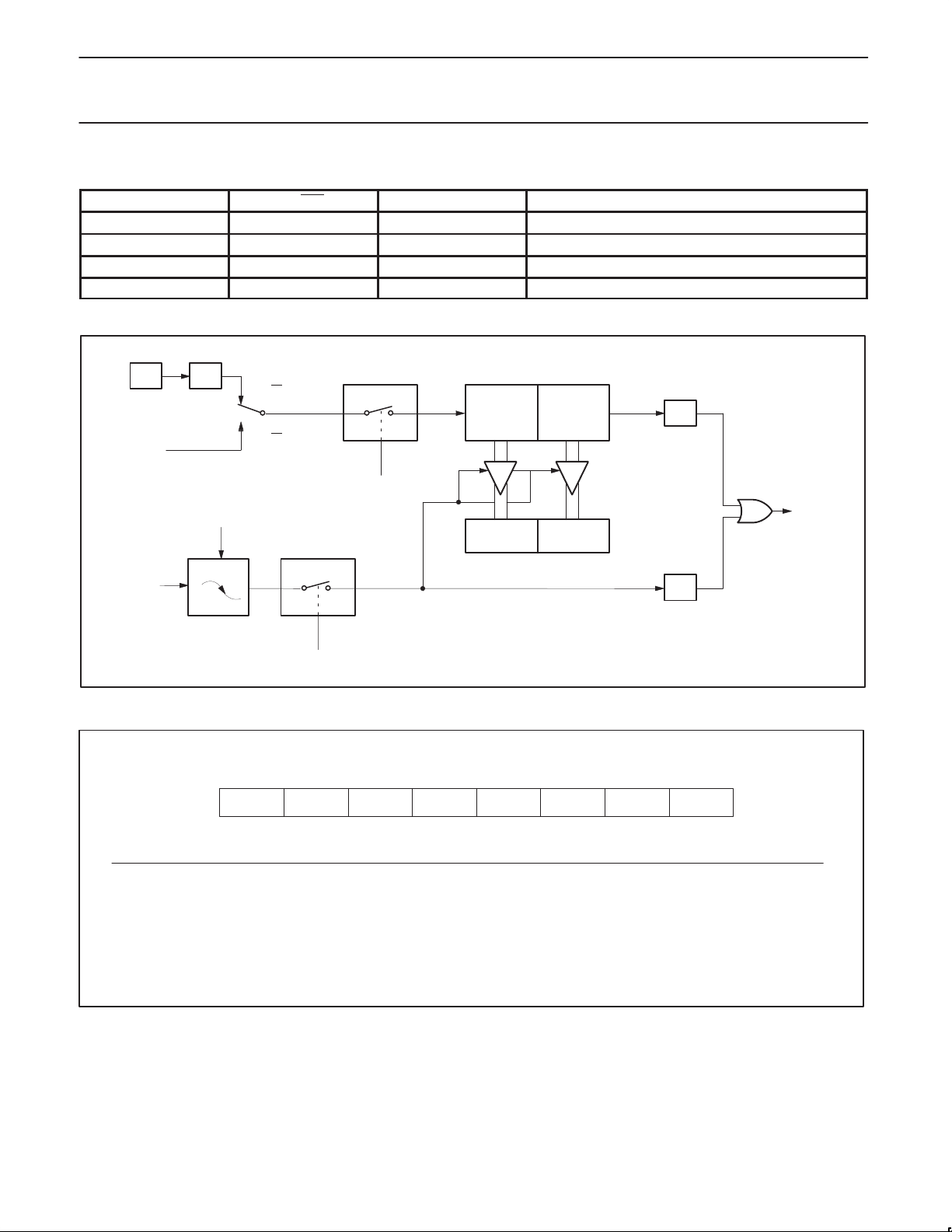
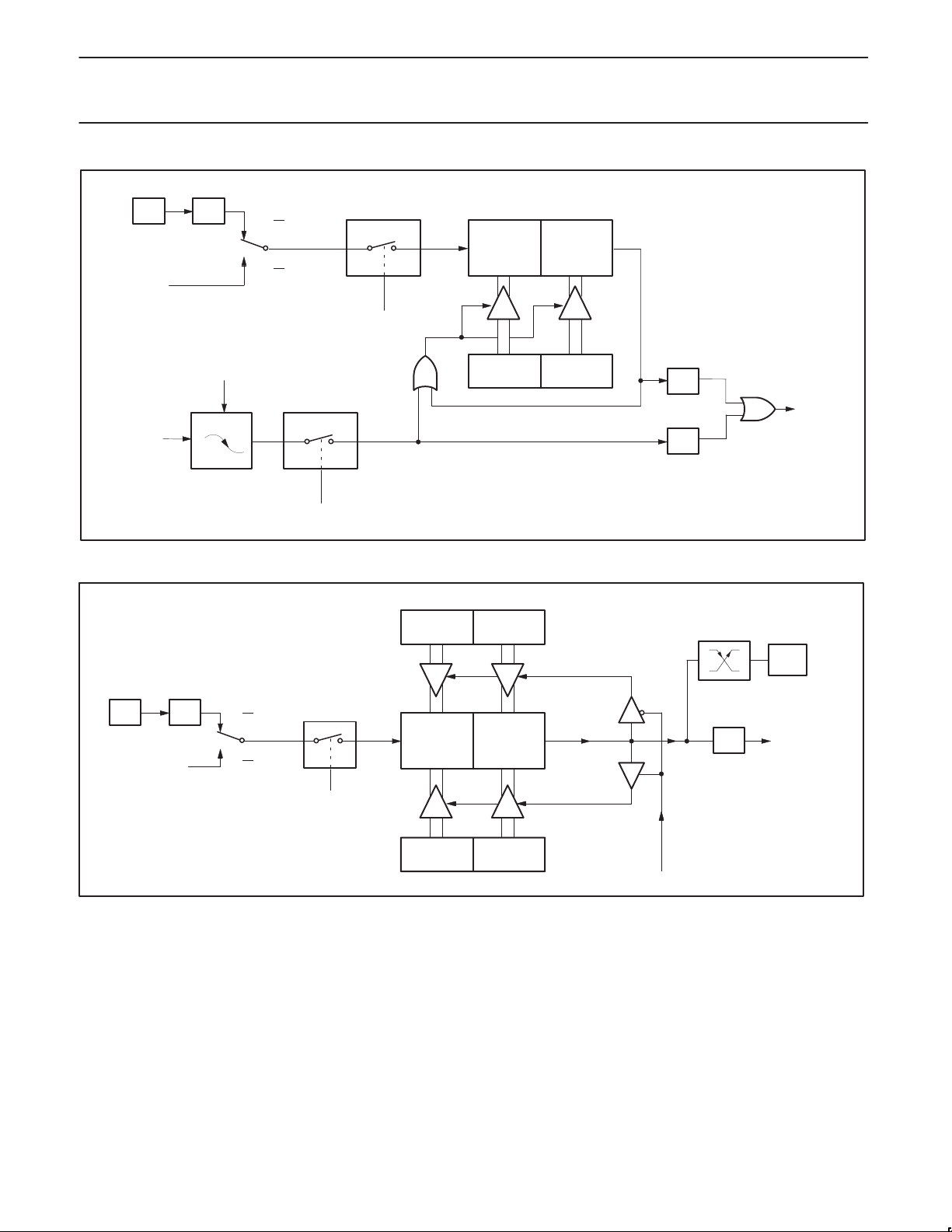
TIMER 2 OPERATION
Timer 2
Timer 2 is a 16-bit Timer/Counter which can operate as either an
event timer or an event counter, as selected by C/T
function register T2CON (see Figure 1). Timer 2 has three operating
modes: Capture, Auto-reload (up or down counting), and Baud Rate
Generator, which are selected by bits in the T2CON as shown in
Table 4.
2* in the special
Capture Mode
In the capture mode there are two options which are selected by bit
EXEN2 in T2CON. If EXEN2=0, then timer 2 is a 16-bit timer or
counter (as selected by C/T
sets bit TF2, the timer 2 overflow bit. This bit can be used to
generate an interrupt (by enabling the Timer 2 interrupt bit in the
IE register). If EXEN2= 1, Timer 2 operates as described above, but
with the added feature that a 1-to-0 transition at external input T2EX
causes the current value in the Timer 2 registers, TL2 and TH2, to
be captured into registers RCAP2L and RCAP2H, respectively. In
addition, the transition at T2EX causes bit EXF2 in T2CON to be
set, and EXF2 like TF2 can generate an interrupt (which vectors to
the same location as Timer 2 overflow interrupt. The Timer 2
interrupt service routine can interrogate TF2 and EXF2 to determine
which event caused the interrupt). The capture mode is illustrated in
Figure 2. (There is no reload value for TL2 and TH2 in this mode.
Even when a capture event occurs from T2EX, the counter keeps on
counting T2EX pin transitions or osc/12 pulses.)
2* in T2CON) which, upon overflowing
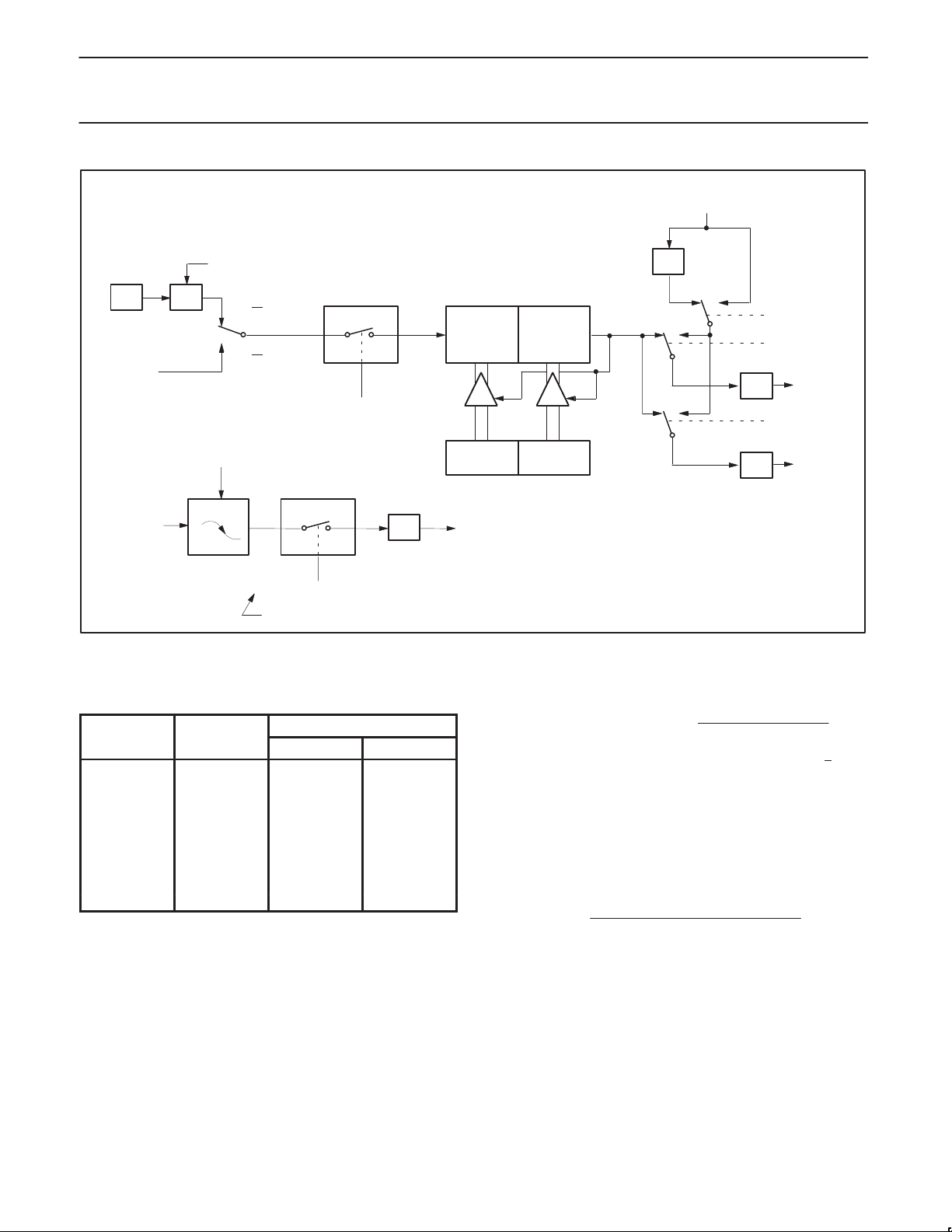
Auto-Reload Mode (Up or Down Counter)
In the 16-bit auto-reload mode, Timer 2 can be configured (as either
a timer or counter [C/T
or down. The counting direction is determined by bit DCEN (Down
Counter Enable) which is located in the T2MOD register (see
2* in T2CON]) then programmed to count up
8XC52/54/58/80C32
8XC51FA/FB/FC/80C51FA
8XC51RA+/RB+/RC+/RD+/80C51RA+
Figure 3). When reset is applied the DCEN=0 which means Timer 2
will default to counting up. If DCEN bit is set, Timer 2 can count up
or down depending on the value of the T2EX pin.
Figure 4 shows Timer 2 which will count up automatically since
DCEN=0. In this mode there are two options selected by bit EXEN2
in T2CON register. If EXEN2=0, then T imer 2 counts up to 0FFFFH
and sets the TF2 (Overflow Flag) bit upon overflow. This causes the
Timer 2 registers to be reloaded with the 16-bit value in RCAP2L
and RCAP2H. The values in RCAP2L and RCAP2H are preset by
software means.
If EXEN2=1, then a 16-bit reload can be triggered either by an
overflow or by a 1-to-0 transition at input T2EX. This transition also
sets the EXF2 bit. The Timer 2 interrupt, if enabled, can be
generated when either TF2 or EXF2 are 1.
In Figure 5 DCEN=1, which enables Timer 2 to count up or down.
This mode allows pin T2EX to control the direction of count. When a
logic 1 is applied at pin T2EX Timer 2 will count up. Timer 2 will
overflow at 0FFFFH and set the TF2 flag, which can then generate
an interrupt, if the interrupt is enabled. This timer overflow also
causes the 16–bit value in RCAP2L and RCAP2H to be reloaded
into the timer registers TL2 and TH2.
When a logic 0 is applied at pin T2EX this causes Timer 2 to count
down. The timer will underflow when TL2 and TH2 become equal to
the value stored in RCAP2L and RCAP2H. Timer 2 underflow sets
the TF2 flag and causes 0FFFFH to be reloaded into the timer
registers TL2 and TH2.
The external flag EXF2 toggles when Timer 2 underflows or
overflows. This EXF2 bit can be used as a 17th bit of resolution if
needed. The EXF2 flag does not generate an interrupt in this mode
of operation.
(MSB) (LSB)
TF2 EXF2 RCLK TCLK EXEN2 TR2 C/T2
Symbol Position Name and Significance
TF2 T2CON.7 Timer 2 overflow flag set by a Timer 2 overflow and must be cleared by software. TF2 will not be set
EXF2 T2CON.6 Timer 2 external flag set when either a capture or reload is caused by a negative transition on T2EX and
RCLK T2CON.5 Receive clock flag. When set, causes the serial port to use Timer 2 overflow pulses for its receive clock
TCLK T2CON.4 Transmit clock flag. When set, causes the serial port to use Timer 2 overflow pulses for its transmit clock
EXEN2 T2CON.3 Timer 2 external enable flag. When set, allows a capture or reload to occur as a result of a negative
TR2 T2CON.2 Start/stop control for Timer 2. A logic 1 starts the timer.
C/T2
CP/RL2
T2CON.1 Timer or counter select. (Timer 2)
T2CON.0 Capture/Reload flag. When set, captures will occur on negative transitions at T2EX if EXEN2 = 1. When
when either RCLK or TCLK = 1.
EXEN2 = 1. When Timer 2 interrupt is enabled, EXF2 = 1 will cause the CPU to vector to the Timer 2
interrupt routine. EXF2 must be cleared by software. EXF2 does not cause an interrupt in up/down
counter mode (DCEN = 1).
in modes 1 and 3. RCLK = 0 causes Timer 1 overflow to be used for the receive clock.
in modes 1 and 3. TCLK = 0 causes Timer 1 overflows to be used for the transmit clock.
transition on T2EX if Timer 2 is not being used to clock the serial port. EXEN2 = 0 causes Timer 2 to
ignore events at T2EX.
0 = Internal timer (OSC/12)
1 = External event counter (falling edge triggered).
cleared, auto-reloads will occur either with Timer 2 overflows or negative transitions at T2EX when
EXEN2 = 1. When either RCLK = 1 or TCLK = 1, this bit is ignored and the timer is forced to auto-reload
on Timer 2 overflow .
Figure 1. Timer/Counter 2 (T2CON) Control Register
CP/RL2
SU00728
1999 Apr 01
14
Philips Semiconductors Product specification
80C51 8-bit microcontroller family
8K–64K/256–1K OTP/ROM/ROMless, low voltage (2.7V–5.5V),
low power, high speed (33MHz)
8XC51RA+/RB+/RC+/RD+/80C51RA+
Table 4. Timer 2 Operating Modes
RCLK + TCLK CP/RL2 TR2 MODE
0 0 1 16-bit Auto-reload
0 1 1 16-bit Capture
1 X 1 Baud rate generator
X X 0 (off)
OSC
T2 Pin
÷ 12
Transition
Detector
C/T2
C/T2
= 0
= 1
TR2
Control
Capture
TL2
(8-bits)
RCAP2L RCAP2H
TH2
(8-bits)
8XC52/54/58/80C32
8XC51FA/FB/FC/80C51FA
TF2
Timer 2
Interrupt
T2EX Pin
Control
EXEN2
EXF2
SU00066
Figure 2. Timer 2 in Capture Mode
T2MOD Address = 0C9H Reset Value = XXXX XX00B
Not Bit Addressable
— — — — — — T2OE DCEN
Bit
76543210
Symbol Function
— Not implemented, reserved for future use.*
T2OE Timer 2 Output Enable bit.
DCEN Down Count Enable bit. When set, this allows Timer 2 to be configured as an up/down counter.
* User software should not write 1s to reserved bits. These bits may be used in future 8051 family products to invoke new features.
In that case, the reset or inactive value of the new bit will be 0, and its active value will be 1. The value read from a reserved bit is
indeterminate.
SU00729
Figure 3. Timer 2 Mode (T2MOD) Control Register
1999 Apr 01
15
Philips Semiconductors Product specification
80C51 8-bit microcontroller family
8K–64K/256–1K OTP/ROM/ROMless, low voltage (2.7V–5.5V),
low power, high speed (33MHz)
OSC
T2 PIN
T2EX PIN
÷ 12
TRANSITION
DETECTOR
C/T2 = 0
= 1
C/T2
EXEN2
CONTROL
TR2
CONTROL
RELOAD
TL2
(8-BITS)
RCAP2L RCAP2H
8XC52/54/58/80C32
8XC51FA/FB/FC/80C51FA
8XC51RA+/RB+/RC+/RD+/80C51RA+
TH2
(8-BITS)
TF2
EXF2
TIMER 2
INTERRUPT
SU00067
OSC
T2 PIN
÷12
C/T2 = 0
= 1
C/T2
Figure 4. Timer 2 in Auto-Reload Mode (DCEN = 0)
(DOWN COUNTING RELOAD VALUE)
FFH FFH
OVERFLOW
TL2 TH2
CONTROL
TR2
RCAP2L RCAP2H
(UP COUNTING RELOAD VALUE) T2EX PIN
Figure 5. Timer 2 Auto Reload Mode (DCEN = 1)
TOGGLE
COUNT
DIRECTION
1 = UP
0 = DOWN
TF2
EXF2
INTERRUPT
SU00730
1999 Apr 01
16
Philips Semiconductors Product specification
Baud Rate
Osc Freq
80C51 8-bit microcontroller family
8K–64K/256–1K OTP/ROM/ROMless, low voltage (2.7V–5.5V),
low power, high speed (33MHz)
NOTE: OSC. Freq. is divided by 2, not 12.
OSC
T2 Pin
T2EX Pin
÷ 2
Transition
Detector
C/T2 = 0
C/T2
= 1
TR2
Control
EXF2
TL2
(8-bits)
RCAP2L RCAP2H
Timer 2
Interrupt
TH2
(8-bits)
8XC52/54/58/80C32
8XC51FA/FB/FC/80C51FA
8XC51RA+/RB+/RC+/RD+/80C51RA+
Timer 1
Overflow
÷ 2
“0” “1”
SMOD
RCLK
÷ 16
÷ 16 TX Clock
RX Clock
TCLK
Reload
“0”“1”
“0”“1”
Control
EXEN2
Note availability of additional external interrupt.
Figure 6. Timer 2 in Baud Rate Generator Mode
Table 5. Timer 2 Generated Commonly Used
Baud Rates
Timer 2
RCAP2H RCAP2L
375K 12MHz FF FF
9.6K 12MHz FF D9
2.8K 12MHz FF B2
2.4K 12MHz FF 64
1.2K 12MHz FE C8
300 12MHz FB 1E
110 12MHz F2 AF
300 6MHz FD 8F
110 6MHz F9 57
Baud Rate Generator Mode
Bits TCLK and/or RCLK in T2CON (Table 5) allow the serial port
transmit and receive baud rates to be derived from either Timer 1 or
Timer 2. When TCLK= 0, Timer 1 is used as the serial port transmit
baud rate generator . When TCLK= 1, Timer 2 is used as the serial
port transmit baud rate generator. RCLK has the same effect for the
serial port receive baud rate. With these two bits, the serial port can
have different receive and transmit baud rates – one generated by
Timer 1, the other by Timer 2.
Figure 6 shows the Timer 2 in baud rate generation mode. The baud
rate generation mode is like the auto-reload mode,in that a rollover
in TH2 causes the Timer 2 registers to be reloaded with the 16-bit
value in registers RCAP2H and RCAP2L, which are preset by
software.
SU00068
The baud rates in modes 1 and 3 are determined by Timer 2’s
overflow rate given below:
Modes 1 and 3 Baud Rates +
Timer 2 Overflow Rate
16
The timer can be configured for either “timer” or “counter” operation.
In many applications, it is configured for “timer” operation (C/T
2*=0).
Timer operation is different for Timer 2 when it is being used as a
baud rate generator.
Usually, as a timer it would increment every machine cycle (i.e., 1/12
the oscillator frequency). As a baud rate generator, it increments
every state time (i.e., 1/2 the oscillator frequency). Thus the baud
rate formula is as follows:
Modes 1 and 3 Baud Rates =
Oscillator Frequency
[32 [65536 * (RCAP2H, RCAP2L)]]
Where: (RCAP2H, RCAP2L)= The content of RCAP2H and
RCAP2L taken as a 16-bit unsigned integer.
The Timer 2 as a baud rate generator mode shown in Figure 6, is
valid only if RCLK and/or TCLK = 1 in T2CON register. Note that a
rollover in TH2 does not set TF2, and will not generate an interrupt.
Thus, the Timer 2 interrupt does not have to be disabled when
Timer 2 is in the baud rate generator mode. Also if the EXEN2
(T2 external enable flag) is set, a 1-to-0 transition in T2EX
(Timer/counter 2 trigger input) will set EXF2 (T2 external flag) but
will not cause a reload from (RCAP2H, RCAP2L) to (TH2,TL2).
Therefore when Timer 2 is in use as a baud rate generator, T2EX
can be used as an additional external interrupt, if needed.
1999 Apr 01
17
 Loading...