

Philips 74lv11 DATASHEETS
INTEGRATED CIRCUITS
74LV11
Triple 3-input AND gate
Product specification
Supersedes data of 1997 Feb 03
IC24 Data Handbook
1998 Apr 20
Philips Semiconductors Product specification
74L V11Triple 3-input AND gate
FEA TURES
•Optimized for Low Voltage applications: 1.0 to 3.6 V
•Accepts TTL input levels between V
•Typical V
T
amb
•Typical V
T
amb
(output ground bounce) 0.8 V at VCC = 3.3 V,
OLP
= 25°C
(output VOH undershoot) 2 V at VCC = 3.3 V,
OHV
= 25°C
= 2.7 V and VCC = 3.6 V
CC
•Output capability: standard
•I
category: SSI
CC
QUICK REFERENCE DATA
GND = 0 V; T
SYMBOL
t
NOTES:
1. C
is used to determine the dynamic power dissipation (PD in µW)
PD
= CPD × V
P
D
f
= input frequency in MHz; CL = output load capacitance in pF;
i
= output frequency in MHz; VCC = supply voltage in V;
f
o
(C
L
2. The condition is V
= 25°C; tr = tf 2.5 ns
amb
PHL/tPLH
C
I
C
PD
2
CC
2
V
fo) = sum of the outputs.
CC
PARAMETER CONDITIONS TYPICAL UNIT
Propagation delay
nA, nB, nC to nY
Input capacitance 3.5 pF
Power dissipation capacitance per gate See Notes 1 and 2 18 pF
× fi (CL × V
= GND to V
I
CC
CC.
2
fo) where:
DESCRIPTION
The 74LV11 is a low-voltage Si-gate CMOS device and is pin and
function compatible with 74HC/HCT11.
The 74LV11 provides the 3-input AND function.
CL = 15 pF;
VCC = 3.3 V
10 ns
ORDERING INFORMATION
PACKAGES TEMPERATURE RANGE OUTSIDE NORTH AMERICA NORTH AMERICA PKG. DWG. #
14-Pin Plastic DIL –40°C to +125°C 74LV11 N 74LV11 N SOT27-1
14-Pin Plastic SO –40°C to +125°C 74LV11 D 74LV11 D SOT108-1
14-Pin Plastic SSOP Type II –40°C to +125°C 74LV11 DB 74LV11 DB SOT337-1
14-Pin Plastic TSSOP Type I –40°C to +125°C 74LV11 PW 74LV11PW DH SOT402-1
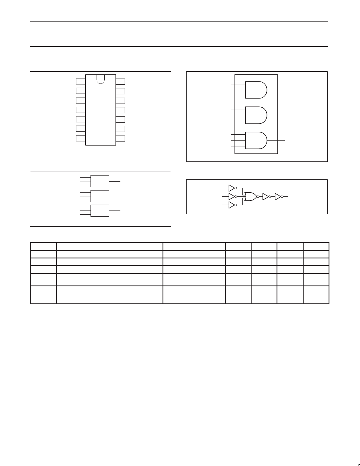
PIN DESCRIPTION
PIN NUMBER SYMBOL NAME AND FUNCTION
1, 3, 9 1A – 3A Data inputs
2, 4, 10 1B – 3B Data inputs
7 GND Ground (0 V)
12, 6, 8 1Y – 3Y Data outputs
13, 5, 11 1C – 3C Data inputs
14 V
CC
Positive supply voltage
FUNCTION TABLE
INPUTS OUTPUT
nA nB nC nY
L L L L
L L H L
L H L L
L H H L
H L L L
H L H L
H H L L
H H H H
NOTES:
H = HIGH voltage level
L = LOW voltage level
1998 Apr 20 853–1894 19256
2
Philips Semiconductors Product specification
74LV11Triple 3-input AND gate
PIN CONFIGURATION
1
1A
2
1B
3
2A
4
2B
5
2C
6
2Y
7
GND
LOGIC SYMBOL (IEEE/IEC)
1
2
13
3
4
5
9
10
11
&
&
&
SV00416
SV00439
LOGIC SYMBOL
V
14
CC
1C
13
1Y
12
3C
11
3B
10
3A
9
3Y
8
1A131
1B2
1C
3
2B4
2C2A5
3A119
3B10
3C
2Y
3Y
SV00438
121Y
6
8
LOGIC DIAGRAM (ONE GATE)
12
A
6
8
B
C
Y
SV00421
RECOMMENDED OPERA TING CONDITIONS
SYMBOL PARAMETER CONDITIONS MIN TYP MAX UNIT
V
V
V
T
amb
tr, t
NOTE:
1. The LV is guaranteed to function down to V
DC supply voltage See Note 1 1.0 3.3 3.6 V
CC
Input voltage 0 – V
I
Output voltage 0 – V
O
Operating ambient temperature range in free air
Input rise and fall times
f
CC
See DC and AC
characteristics
VCC = 1.0V to 2.0V
VCC = 2.0V to 2.7V
VCC = 2.7V to 3.6V
= 1.0V (input levels GND or VCC); DC characteristics are guaranteed from VCC = 1.2V to VCC = 3.6V.
–40
–40
–
–
–
–
–
–
CC
CC
+85
+125
500
200
100
ns/V
V
V
°C
1998 Apr 20
3
 Loading...