

Philips 74HCT597U, 74HCT597N, 74HCT597DB, 74HC597U, 74HC597PW Datasheet
...
DATA SH EET
Product specification
File under Integrated Circuits, IC06
December 1990
INTEGRATED CIRCUITS
74HC/HCT597
8-bit shift register with input
flip-flops
For a complete data sheet, please also download:
•The IC06 74HC/HCT/HCU/HCMOS Logic Family Specifications
•The IC06 74HC/HCT/HCU/HCMOS Logic Package Information
•The IC06 74HC/HCT/HCU/HCMOS Logic Package Outlines
December 1990 2
Philips Semiconductors Product specification
8-bit shift register with input flip-flops 74HC/HCT597
FEATURES
• 8-bit parallel storage register inputs
• Shift register has direct overriding load and clear
• Output capability: standard
• ICC category: MSI
GENERAL DESCRIPTION
The 74HC/HCT597 are high-speed Si-gate CMOS devices
and are pin compatible with low power Schottky TTL
(LSTTL). They are specified in compliance with JEDEC
standard no. 7A.
The 74HC/HCT597 consist each of an 8-bit storage
register feeding a parallel-in, serial-out 8-bit shift register.
Both the storage register and the shift register have
positive edge-triggered clocks. The shift register also has
direct load (from storage) and clear inputs.
QUICK REFERENCE DATA
GND = 0 V; T
amb
=25°C; tr=tf= 6 ns
Notes
1. C
PD
is used to determine the dynamic power dissipation (PD in µW):
PD=CPD× V
CC
2
× fi+ ∑ (CL× V
CC
2
× fo) where:
fi= input frequency in MHz
fo= output frequency in MHz
∑ (CL× V
CC
2
× fo) = sum of outputs
CL= output load capacitance in pF
VCC= supply voltage in V
2. For HC the condition is VI= GND to V
CC
For HCT the condition is VI= GND to VCC− 1.5 V
ORDERING INFORMATION
See
“74HC/HCT/HCU/HCMOS Logic Package Information”
.
SYMBOL PARAMETER CONDITIONS
TYPICAL
UNIT
HC HCT
t
PHL
/ t
PLH
propagation delay CL= 15 pF; VCC=5V
SH
CP
to Q 17 20 ns
ST
CP
to Q 25 29 ns
PL to Q 21 26 ns
f
max
maximum clock frequency SH
CP
96 83 MHz
C
I
input capacitance 3.5 3.5 pF
C
PD
power dissipation capacitance per package notes 1 and 2 29 32 pF
December 1990 3
Philips Semiconductors Product specification
8-bit shift register with input flip-flops 74HC/HCT597
PIN DESCRIPTION
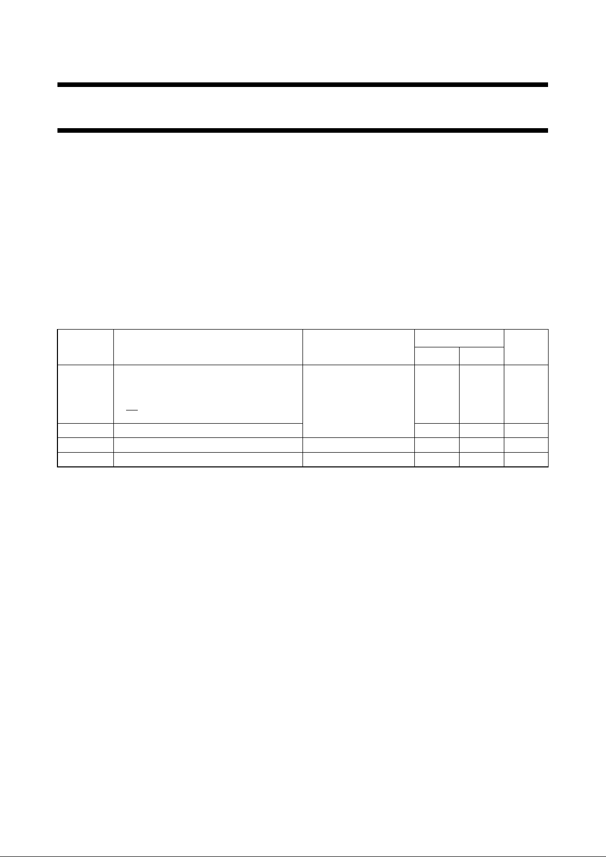
PIN NO. SYMBOL NAME AND FUNCTION
8 GND ground (0 V)
9 Q serial data output
10
MR asynchronous reset input (active LOW)
11 SH
CP
shift clock input (LOW-to-HIGH, edge-triggered)
12 ST
CP
storage clock input (LOW-to-HIGH, edge-triggered)
13
PL parallel load input (active LOW)
14 D
S
serial data input
15, 1, 2, 3, 4, 5, 6, 7 D
0
to D
7
parallel data inputs
16 V
CC
positive supply voltage
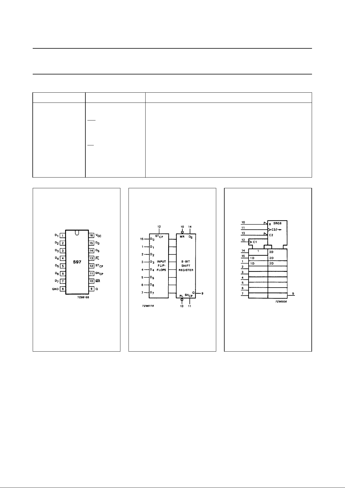
Fig.1 Pin configuration. Fig.2 Logic symbol. Fig.3 IEC logic symbol.
December 1990 4
Philips Semiconductors Product specification
8-bit shift register with input flip-flops 74HC/HCT597
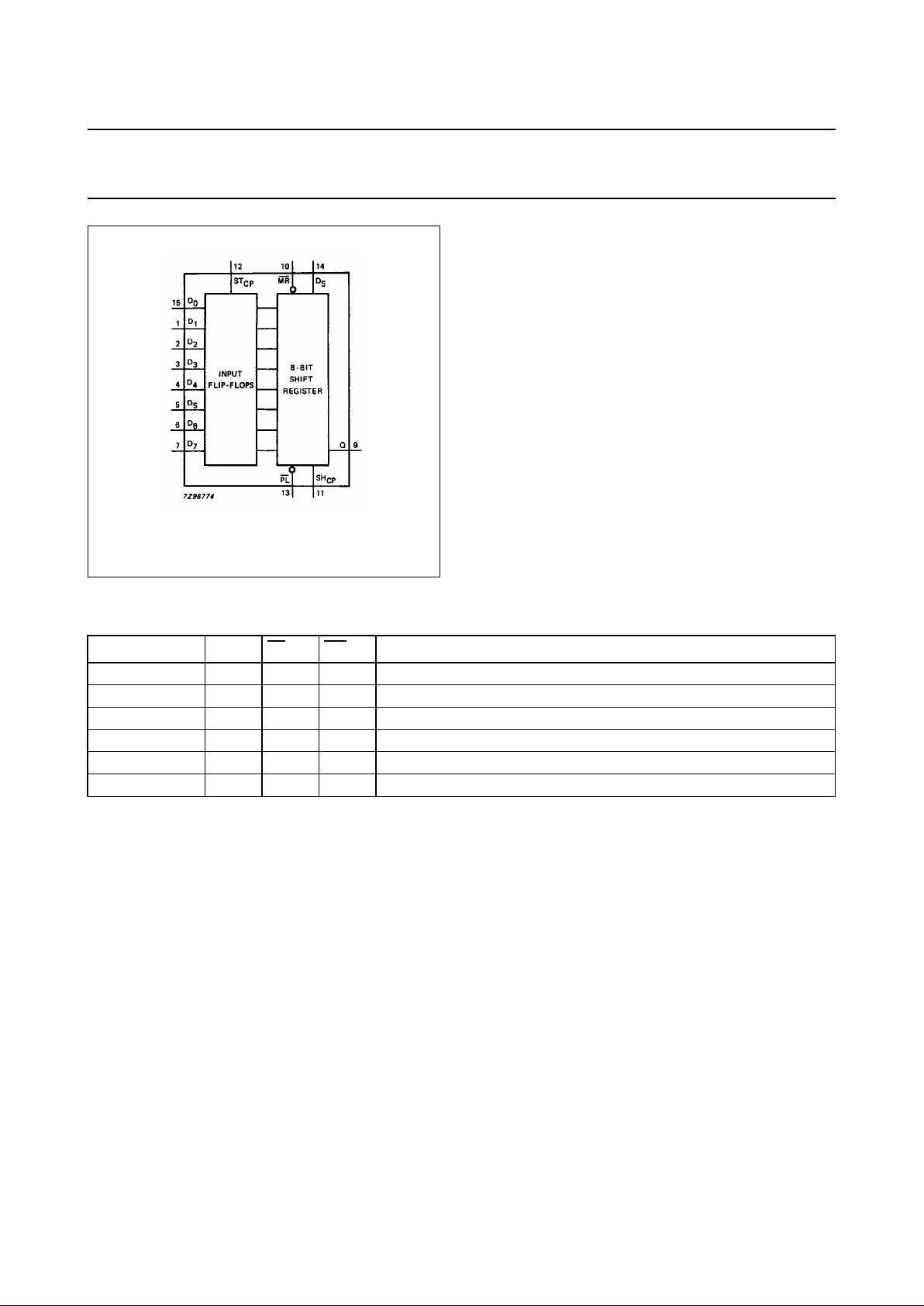
FUNCTION TABLE
Notes
1. H = HIGH voltage level
L = LOW voltage level
X = don’t care
↑ = LOW-to-HIGH CP transition
ST
CP
SH
CP
PL MR FUNCTION
↑ X X X data loaded to input latches
↑ X L H data loaded from inputs to shift register
no clock edge X L H data transferred from input flip-flops to shift register
X X L L invalid logic, state of shift register indeterminate when signals removed
X X H L shift register cleared
X ↑ H H shift register clocked Q
n=Qn−1
, Q0=D
S
Fig.4 Functional diagram.
 Loading...