

Philips 74HCT595N, 74HCT595DB, 74HCT595D, 74HCT595PW, 74HC595U Datasheet
...
DATA SH EET
Product specification
Supersedes data of September 1993
File under Integrated Circuits, IC06
1998 Jun 04
INTEGRATED CIRCUITS
74HC/HCT595
8-bit serial-in/serial or parallel-out
shift register with output latches;
3-state
For a complete data sheet, please also download:
•The IC06 74HC/HCT/HCU/HCMOS Logic Family Specifications
•The IC06 74HC/HCT/HCU/HCMOS Logic Package Information
•The IC06 74HC/HCT/HCU/HCMOS Logic Package Outlines

1998 Jun 04 2
Philips Semiconductors Product specification
8-bit serial-in/serial or parallel-out shift
register with output latches; 3-state
74HC/HCT595
FEATURES
• 8-bit serial input
• 8-bit serial or parallel output
• Storage register with 3-state outputs
• Shift register with direct clear
• 100 MHz (typ) shift out frequency
• Output capability:
– parallel outputs; bus driver
– serial output; standard
• ICC category: MSI.
APPLICATIONS
• Serial-to-parallel data conversion
• Remote control holding register.
DESCRIPTION
The 74HC/HCT595 are high-speed Si-gate CMOS devices
and are pin compatible with low power Schottky TTL
(LSTTL). They are specified in compliance with JEDEC
standard no. 7A.
The “595” is an 8-stage serial shift register with a storage
register and 3-state outputs. The shift register and storage
register have separate clocks.
Data is shifted on the positive-going transitions of the
SHCP input. The data in each register is transferred to the
storage register on a positive-going transition of the ST
CP
input. If both clocks are connected together, the shift
register will always be one clock pulse ahead of the
storage register.
The shift register has a serial input (DS) and a serial
standard output (Q7’) for cascading. It is also provided with
asynchronous reset (active LOW) for all 8 shift register
stages. The storage register has 8 parallel 3-state bus
driver outputs. Data in the storage register appears at the
output whenever the output enable input (OE) is LOW.
QUICK REFERENCE DATA
GND = 0 V; T
amb
=25°C; tr=tf= 6 ns.
Notes
1. C
PD
is used to determine the dynamic power dissipation (PD in µW):
PD=CPD× V
CC
2
× fi+∑ (CL× V
CC
2
× fo) where:
fi= input frequency in MHz
fo= output frequency in MHz
∑(CL× V
CC
2
× fo) = sum of outputs
CL= output load capacitance in pF
VCC= supply voltage in V
2. For HC the condition is VI= GND to VCC; for HCT the condition is VI= GND to VCC− 1.5 V.
SYMBOL PARAMETER CONDITIONS
TYP.
UNIT
HC HCT
t
PHL/tPLH
propagation delay CL= 15 pF; VCC=5V
SH
CP
to Q7’ 1621ns
ST
CP
to Q
n
17 20 ns
MR to Q7’ 1419ns
f
max
maximum clock frequency SHCP, ST
CP
100 57 MHz
C
I
input capacitance 3.5 3.5 pF
C
PD
power dissipation capacitance per package notes 1 and 2 115 130 pF

1998 Jun 04 3
Philips Semiconductors Product specification
8-bit serial-in/serial or parallel-out shift
register with output latches; 3-state
74HC/HCT595
ORDERING INFORMATION
PINNING
TYPE NUMBER
PACKAGE
NAME DESCRIPTION VERSION
74HC595N DIP16 plastic dual in-line package; 16 leads (300 mil); long body SOT38-1
74HC595D SO16 plastic small outline package; 16 leads; body width 3.9 mm SOT109-1
74HC595DB SSOP16 plastic shrink small outline package; 16 leads; body width 5.3 mm SOT338-1
74HC595PW TSSOP16 plastic thin shrink small outline package; 16 leads; body width 4.4 mm SOT403-1
74HCT595N DIP16 plastic dual in-line package; 16 leads (300 mil); long body SOT38-1
74HCT595D SO16 plastic small outline package; 16 leads; body width 3.9 mm SOT109-1
SYMBOL PIN DESCRIPTION
Q
0
to Q
7
15, 1 to 7 parallel data output
GND 8 ground (0 V)
Q
7
’ 9 serial data output
MR 10 master reset (active LOW)
SH
CP
11 shift register clock input
ST
CP
12 storage register clock input
OE 13 output enable (active LOW)
D
S
14 serial data input
V
CC
16 positive supply voltage
Fig.1 Pin configuration.
handbook, halfpage
Q
1
Q
2
Q
3
Q
4
Q
5
Q
6
Q
7
Q7'
Q
0
D
S
GND
ST
CP
SH
CP
V
CC
OE
1
2
3
4
5
6
7
8
16
15
14
13
12
11
10
9
595
MLA001
MR
Fig.2 Logic symbol.
handbook, halfpage
OEMR
9
15
1
2
3
4
5
6
7
1310
14
11 12
MLA002
Q
1
Q
0
Q
2
Q
3
Q
4
Q
5
Q
6
Q
7
Q7'
D
S
ST
CP
SH
CP

1998 Jun 04 4
Philips Semiconductors Product specification
8-bit serial-in/serial or parallel-out shift
register with output latches; 3-state
74HC/HCT595
Fig.3 IEC logic symbol.
handbook, halfpage
MSA698
15
9
1
2
3
4
5
6
7
1D 2D
C1/
10
11
14
C2
12
13
EN3
SRG8
R
3
OE
MR
Q
1
Q
0
Q
2
Q
3
Q
4
Q
5
Q
6
Q
7
Q7'
D
S
ST
CP
SH
CP
Fig.4 Functional diagram.
handbook, full pagewidth
ST
CP
D
S
SH
CP
MR
Q7'
8-STAGE SHIFT REGISTER
8-BIT STORAGE REGISTER
14
11
10
12
9
OE
3-STATE OUTPUTS
Q
1
Q
2
Q
3
Q
5
Q
6
Q
7
Q
4
Q
0
15
1
2
3
4
5
6
7
13
MLA003
1998 Jun 04 5
Philips Semiconductors Product specification
8-bit serial-in/serial or parallel-out shift
register with output latches; 3-state
74HC/HCT595
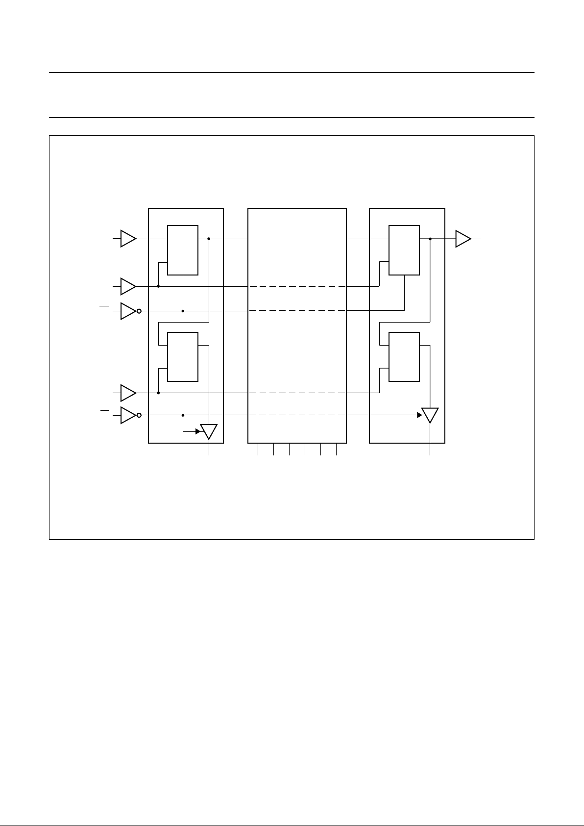
Fig.5 Logic diagram.
handbook, full pagewidth
STAGE 0 STAGES 1 TO 6 STAGE 7
FF0
DCPQ
R
LATCH
DCPQ
FF7
DCPQ
R
LATCH
DCPQ
MLA010
DQ
Q
1
Q
2
Q
3
Q
4
Q
5
Q
6
Q
7
Q
7
'
Q
0
D
S
ST
CP
SH
CP
OE
MR

1998 Jun 04 6
Philips Semiconductors Product specification
8-bit serial-in/serial or parallel-out shift
register with output latches; 3-state
74HC/HCT595
FUNCTION TABLE
Notes
1. H = HIGH voltage level; L = LOW voltage level
↑ = LOW-to-HIGH transition; ↓ = HIGH-to-LOW transition
Z = high-impedance OFF-state; NC = no change
X = don’t care.
INPUTS OUTPUTS
FUNCTON
SH
CP
ST
CP
OE MR D
S
Q7’Q
N
X X L L X L NC a LOW level on MR only affects the shift registers
X ↑ L L X L L empty shift register loaded into storage register
X X H L X L Z shift register clear. Parallel outputs in high-impedance
OFF-state
↑ XLHHQ
6
’ NC logic high level shifted into shift register stage 0. Contents
of all shift register stages shifted through, e.g. previous
state of stage 6 (internal Q
6
’) appears on the serial output
(Q7’)
X ↑ LHXNCQ
n
’ contents of shift register stages (internal Qn’) are
transferred to the storage register and parallel output
stages
↑↑LHXQ
6
’Qn’ contents of shift register shifted through. Previous
contents of the shift register is transferred to the storage
register and the parallel output stages.
 Loading...