


INTEGRATED CIRCUITS
DATA SH EET
74HC595; 74HCT595
8-bit serial-in, serial or parallel-out
shift register with output latches;
3-state
Product specification
Supersedes data of 1998 Jun 04
2003 Jun 25
Philips Semiconductors Product specification
8-bit serial-in, serial or parallel-out shift
register with output latches; 3-state
FEATURES
• 8-bit serial input
• 8-bit serial or parallel output
• Storage register with 3-state outputs
• Shift register with direct clear
• 100 MHz (typical) shift out frequency
• ESD protection:
HBM EIA/JESD22-A114-A exceeds 2000 V
MM EIA/JESD22-A115-A exceeds 200 V.
APPLICATIONS
• Serial-to-parallel data conversion
• Remote control holding register.
74HC595; 74HCT595
DESCRIPTION
The74HC/HCT595arehigh-speedSi-gateCMOSdevices
and are pin compatible with low power Schottky TTL
(LSTTL). They are specified in compliance with JEDEC
standard no. 7A.
The 74HC/HCT595 is an 8-stage serialshift register witha
storage register and3-state outputs. The shift register and
storage register have separate clocks.
Data is shifted on the positive-going transitions of the
SH_CP input. The data in each register is transferred to
the storage register on a positive-going transition of the
ST_CP input. If both clocks are connected together, the
shift register will always be one clock pulse ahead of the
storage register.
The shift register has a serial input (DS) and a serial
standard output (Q7’) for cascading. It is also provided
with asynchronous reset (active LOW) for all 8 shift
register stages. The storage register has 8 parallel 3-state
bus driver outputs. Data in the storage register appears at
the output whenever the output enable input (OE) is LOW.
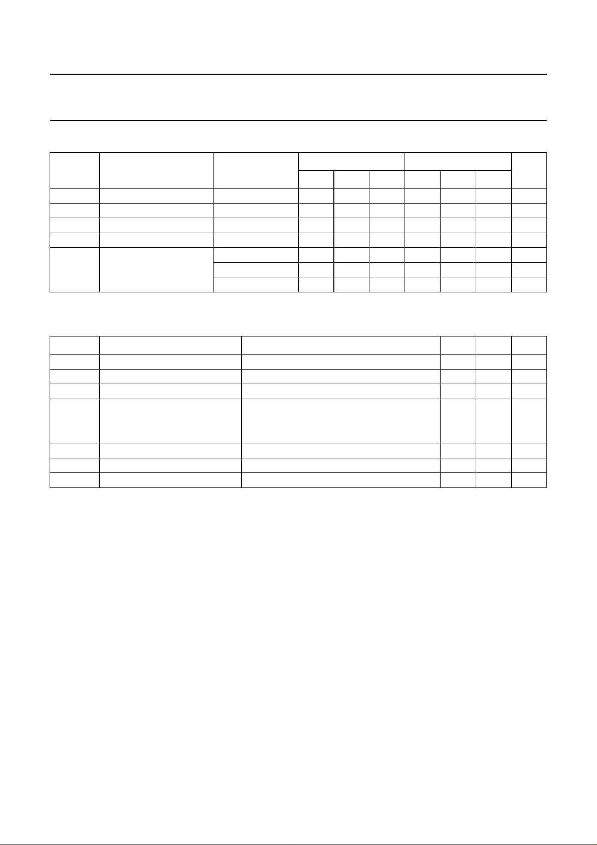
QUICK REFERENCE DATA
GND = 0 V; T
=25°C; tr=tf= 6 ns.
amb
SYMBOL PARAMETER CONDITIONS
t
PHL/tPLH
propagation delay CL= 50 pF; VCC= 4.5 V
SH_CP to Q7’ 19 25 ns
SH_CP to Qn 20 24 ns
MR to Q7’ 100 52 ns
f
max
C
C
I
PD
maximum clock frequency SH_CPand ST_CP 100 57 MHz
input capacitance 3.5 3.5 pF
power dissipation capacitance per package notes 1 and 2 115 130 pF
Notes
1. C
is used to determine the dynamic power dissipation (PDin µW).
PD
PD=CPD× V
2
× fi× N+Σ(CL× V
CC
2
× fo) where:
CC
fi= input frequency in MHz;
fo= output frequency in MHz;
CL= output load capacitance in pF;
VCC= supply voltage in Volts;
N = total load switching outputs;
Σ(CL× V
2
× fo) = sum of the outputs.
CC
2. For 74HC595 the condition is VI= GND to VCC.
For 74HCT595 the condition is VI= GND to VCC− 1.5 V.
TYPICAL
UNIT
74HC 74HCT
2003 Jun 25 2
Philips Semiconductors Product specification
8-bit serial-in, serial or parallel-out shift
74HC595; 74HCT595
register with output latches; 3-state
FUNCTION TABLE
See note 1.
INPUT OUTPUT
SH_CP ST_CP
X X L L X L n.c. a LOW level on
X ↑ L L X L L empty shift register loaded into storage register
X X H L X L Z shift register clear; parallel outputs in high-impedance
↑ X L H H Q6’ n.c. logic high level shifted into shift register stage 0;
X ↑ L H X n.c. Qn’ contents of shift register stages (internal Qn’) are
↑↑L H X Q6’ Qn’ contents of shift register shifted through; previous
OE MR DS Q7’ Qn
OFF-state
contents of allshift registerstages shifted through, e.g.
previous state of stage 6 (internal Q6’) appears on the
serial output (Q7’)
transferred to the storage register and parallel output
stages
contents of the shift register is transferred to the
storage register and the parallel output stages
FUNCTION
MR only affects the shift registers
Note
1. H = HIGH voltage level;
L = LOW voltage level;
↑ = LOW-to-HIGH transition;
↓ = HIGH-to-LOW transition;
Z = high-impedance OFF-state;
n.c. = no change;
X = don’t care.
ORDERING INFORMATION
PACKAGE
TYPE NUMBER
74HC595N −40 to +125 °C 16 DIP16 plastic SOT38-4
74HCT595N −40 to +125 °C 16 DIP16 plastic SOT38-4
74HC595D −40 to +125 °C 16 SO16 plastic SOT109-1
74HCT595D −40 to +125 °C 16 SO16 plastic SOT109-1
74HC595DB −40 to +125 °C 16 SSOP16 plastic SOT338-1
74HCT595DB −40 to +125 °C 16 SSOP16 plastic SOT338-1
74HC595PW −40 to +125 °C 16 TSSOP16 plastic SOT403-1
74HCT595PW −40 to +125 °C 16 TSSOP16 plastic SOT403-1
74HC595BQ −40 to +125 °C 16 DHVQFN16 plastic SOT763-1
74HCT595BQ −40 to +125 °C 16 DHVQFN16 plastic SOT763-1
TEMPERATURE
RANGE
PINS PACKAGE MATERIAL CODE
2003 Jun 25 3
Philips Semiconductors Product specification
8-bit serial-in, serial or parallel-out shift
register with output latches; 3-state
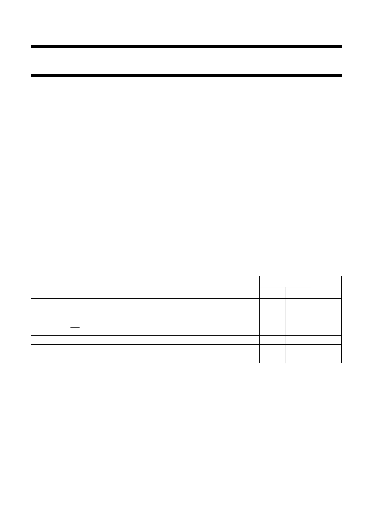
PINNING
PIN SYMBOL DESCRIPTION
1 Q1 parallel data output
2 Q2 parallel data output
3 Q3 parallel data output
4 Q4 parallel data output
5 Q5 parallel data output
6 Q6 parallel data output
7 Q7 parallel data output
8 GND ground (0 V)
9 Q7’ serial data output
10
11 SH_CP shift register clock input
12 ST_CP storage register clock input
13
14 DS serial data input
15 Q0 parallel data output
16 V
MR master reset (active LOW)
OE output enable (active LOW)
CC
positive supply voltage
74HC595; 74HCT595
handbook, halfpage
Q1
Q2
Q3
Q4
Q5
Q6
Q7
GND
1
2
3
4
595
5
6
7
8
MLA001
16
15
14
13
12
11
10
9
V
Q0
DS
OE
ST_CP
SH_CP
MR
Q7'
Fig.1 Pin configuration DIP16, SO16 and
(T)SSOP16.
CC
V
handbook, halfpage
2
Q2
3
Q3
Q4
4
5
Q5
611
Q6
7
Q7
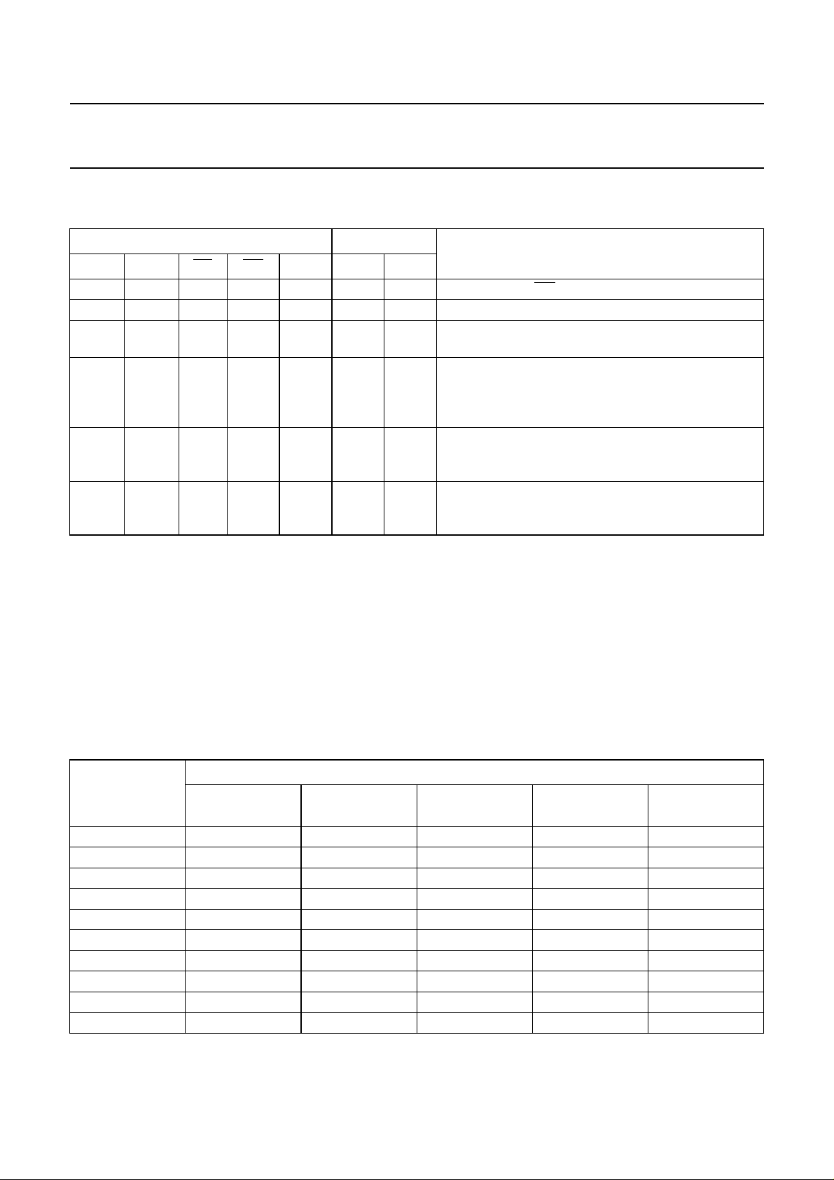
Top view
(1) The die substrate is attached to this pad using conductive die
attach material. It can not be used as a supply pin or input.
Q1
CC
116
(1)
GND
9
8
GND
Q7'
MBL893
15
Q0
14
DS
13
OE
12
ST_CP
SH_CP
10
MR
Fig.2 Pin configuration DHVQFN16.
2003 Jun 25 4
Philips Semiconductors Product specification
8-bit serial-in, serial or parallel-out shift
register with output latches; 3-state
handbook, halfpage
14
SH_CP
DS
11 12
ST_CP
Q7'
OEMR
1310
Q0
Q1
Q2
Q3
Q4
Q5
Q6
Q7
9
15
1
2
3
4
5
6
7
MLA002
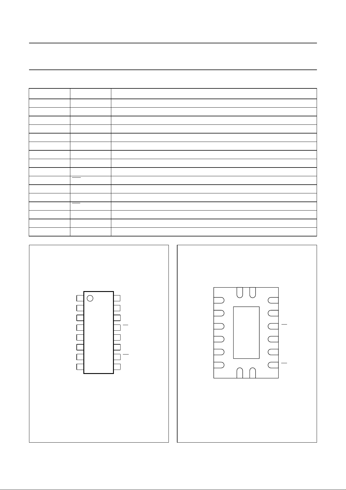
handbook, halfpage
OE
ST_CP
MR
SH_CP
DS
13
12
10
R
11
14
1D 2D
74HC595; 74HCT595
EN3
C2
SRG8
C1/
15
3
MSA698
Q0
1
Q1
2
Q2
3
Q3
4
Q4
5
Q5
6
Q6
7
Q7
9
Q7'
handbook, full pagewidth
Fig.3 Logic symbol.
Fig.4 IEC logic symbol.
14
DS
SH_CP
11
10
MR
ST_CP
12
OE
13
8-STAGE SHIFT REGISTER
8-BIT STORAGE REGISTER
3-STATE OUTPUTS
Q7'
Q0
Q1
Q2
Q3
Q4
Q5
Q6
Q7
9
15
1
2
3
4
5
6
7
Fig.5 Functional diagram.
2003 Jun 25 5
MLA003
Philips Semiconductors Product specification
8-bit serial-in, serial or parallel-out shift
register with output latches; 3-state
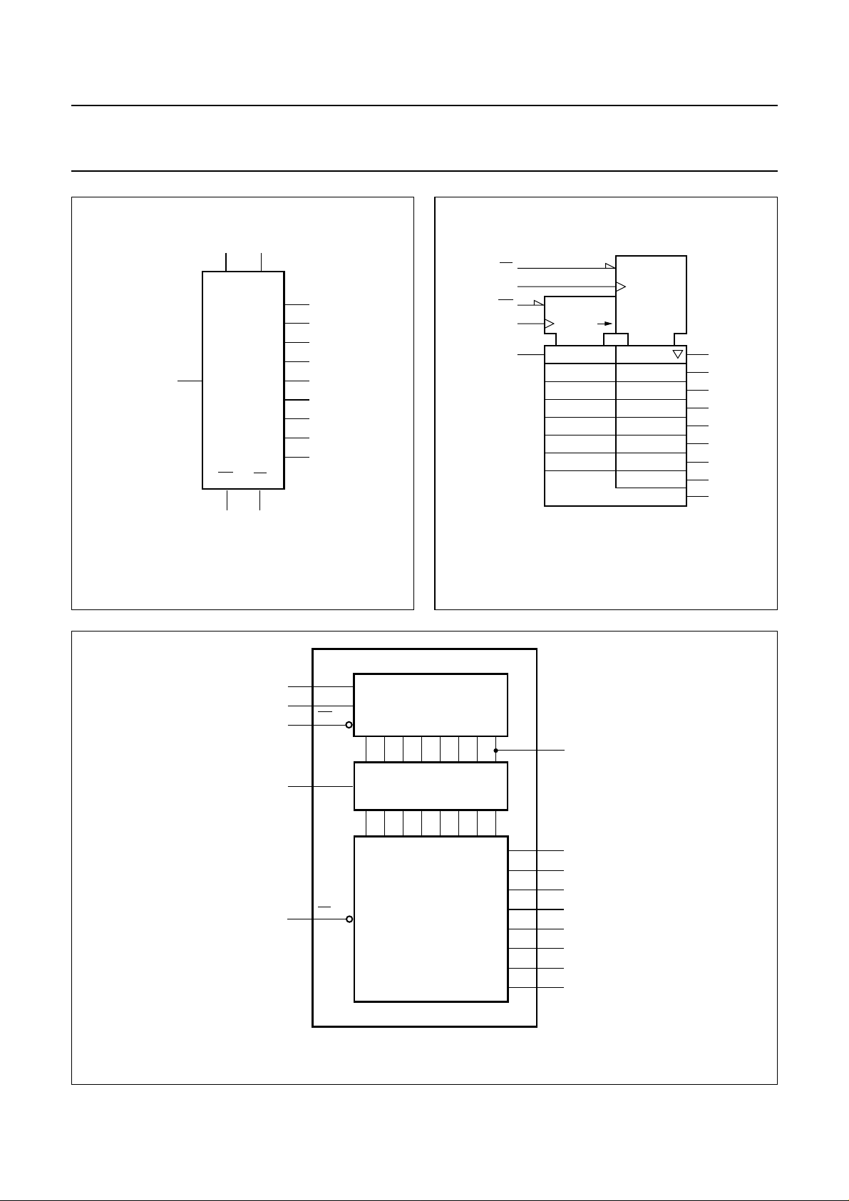
handbook, full pagewidth
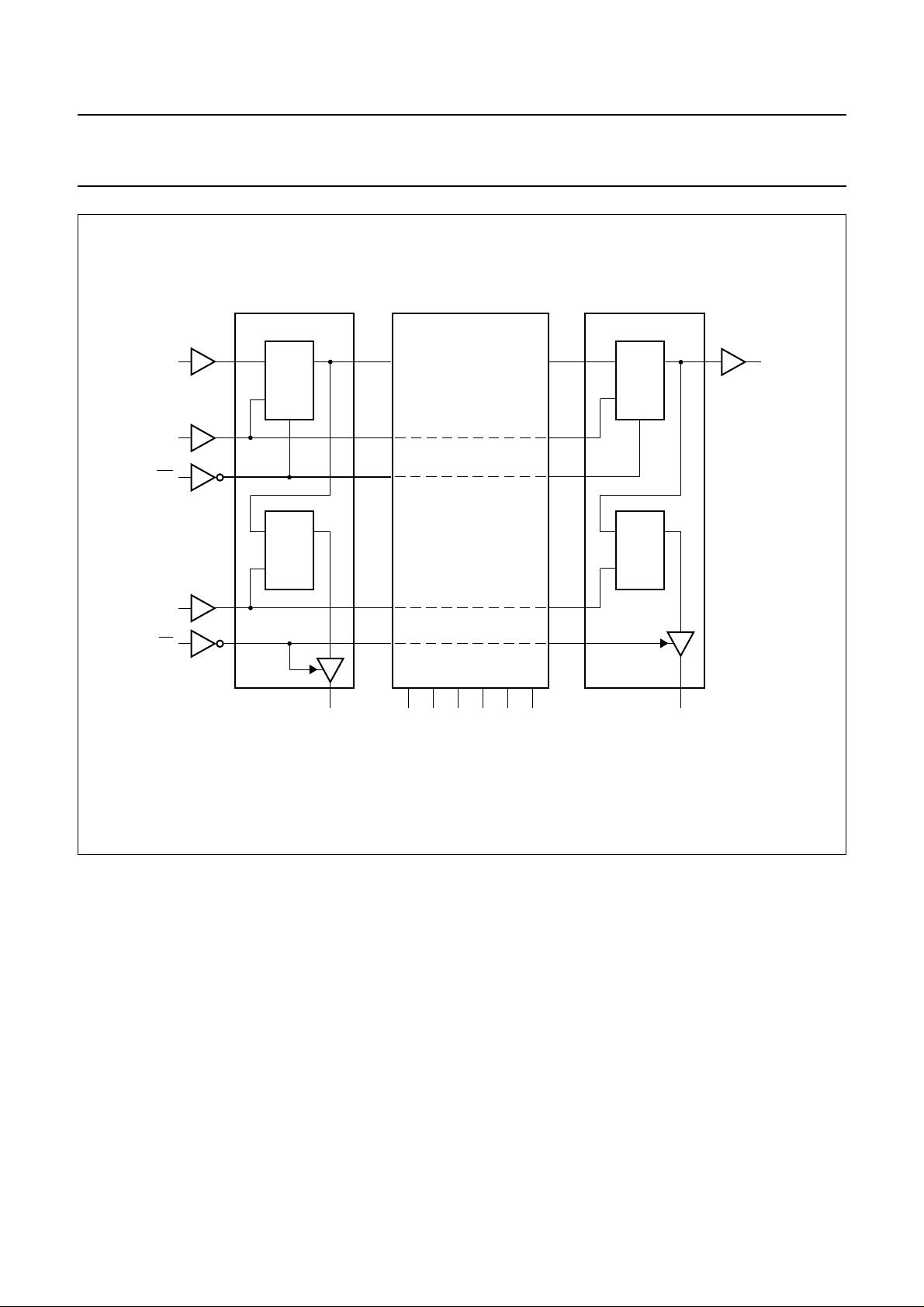
DS
SH_CP
MR
STAGE 0 STAGES 1 to 6 STAGE 7
DCPQ
FF0
R
DCPQ
LATCH
DQ
74HC595; 74HCT595
DCPQ
FF7
R
DCPQ
LATCH
Q7'
ST_CP
OE
Q0
Q1 Q2 Q3 Q4 Q5 Q6 Q7
Fig.6 Logic diagram.
MLA010
2003 Jun 25 6
Philips Semiconductors Product specification
8-bit serial-in, serial or parallel-out shift
register with output latches; 3-state
handbook, full pagewidth
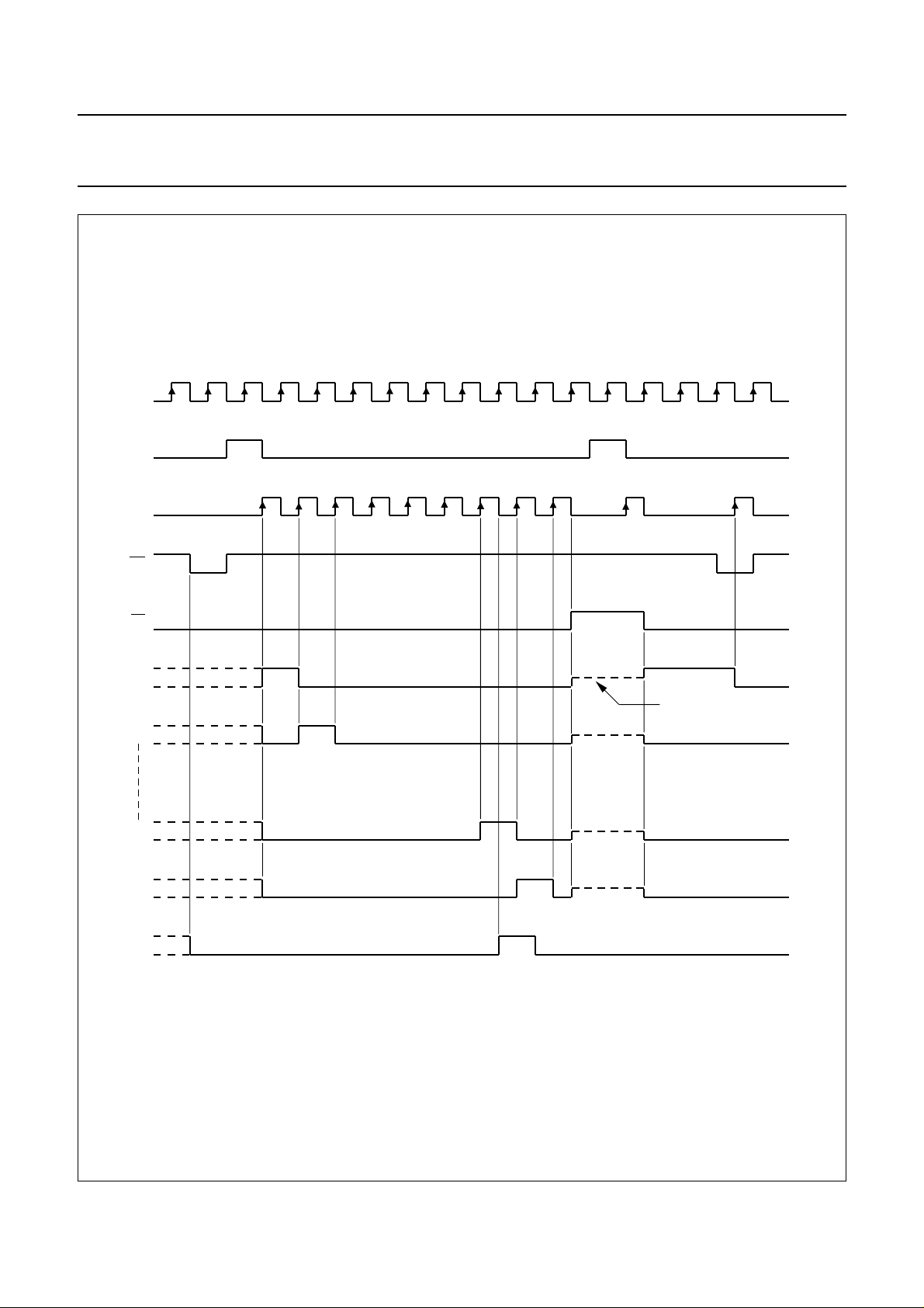
SH_CP
DS
ST_CP
MR
74HC595; 74HCT595
Q0
Q1
Q6
Q7
Q7'
OE
high-impedance OFF-state
MLA005-1
Fig.6 Timing diagram.
2003 Jun 25 7
Philips Semiconductors Product specification
8-bit serial-in, serial or parallel-out shift
74HC595; 74HCT595
register with output latches; 3-state
RECOMMENDED OPERATING CONDITIONS
SYMBOL PARAMETER CONDITIONS
MIN. TYP. MAX. MIN. TYP. MAX.
V
V
V
T
t
r,tf
CC
I
O
amb
supply voltage 2.0 5.0 6.0 4.5 5.0 5.5 V
input voltage 0 − V
output voltage 0 − V
ambient temperature −40 − +125 −40 − +125 °C
input rise and fall time VCC= 2.0 V −−1000 −−−ns
V
= 4.5 V − 6.0 500 − 6.0 500 ns
CC
V
= 6.0 V −−400 −−−ns
CC
LIMITED VALUES
In accordance with the Absolute Maximum Rating System (IEC 60134); voltages are referenced to GND (ground = 0 V).
SYMBOL PARAMETER CONDITIONS MIN. MAX. UNIT
V
CC
I
IK
I
OK
I
O
supply voltage −0.5 +7.0 V
input diode current VI< −0.5 V to VI>VCC+ 0.5 V −±20 mA
output diode current VO< −0.5 V to VO>VCC+ 0.5 V −±20 mA
output source or sink current VO= −0.5 V to VCC+ 0.5 V
Q7’ standard output −±25 mA
Qn bus driver outputs −±35 mA
I
, I
CC
T
stg
P
tot
GNDVCC
or GND current −±70 mA
storage temperature −65 +150 °C
power dissipation T
= −40 to +125 °C; note 1 − 500 mW
amb
74HC 74HCT
0 − V
CC
0 − V
CC
CC
CC
UNIT
V
V
Note
1. For DIP16 packages: above 70 °C derate linearly with 12 mW/K.
For SO16 packages: above 70 °C derate linearly with 8 mW/K.
For SSOP16 packages: above 60 °C derate linearly with 5.5 mW/K.
For TSSOP16 packages: above 60 °C derate linearly with 5.5 mW/K.
For DHVQFN16 packages: above 60 °C derate linearly with 4.5 mW/K.
2003 Jun 25 8
Philips Semiconductors Product specification
8-bit serial-in, serial or parallel-out shift
74HC595; 74HCT595
register with output latches; 3-state
DC CHARACTERISTICS
Type 74HC
At recommended operating conditions; voltages are referenced to GND (ground=0V).
SYMBOL PARAMETER
T
= −40 to +85 °C; note 1
amb
V
IH
HIGH-level input
voltage
V
IL
LOW-level input
voltage
V
OH
HIGH-level output
voltage
V
OL
LOW-level output
voltage
I
LI
I
OZ
input leakage current VI=VCCor GND 6.0 −−±1.0 µA
3-state output
OFF-state current
I
CC
quiescent supply
current
TEST CONDITIONS
MIN. TYP. MAX. UNIT
OTHER V
CC
(V)
2.0 1.5 1.2 − V
4.5 3.15 2.4 − V
6.0 4.2 3.2 − V
2.0 − 0.8 0.5 V
4.5 − 2.1 1.35 V
6.0 − 2.8 1.8 V
VI=VIH or V
IL
all outputs
I
= −20 µA 2.0 1.9 2.0 − V
O
4.5 4.4 4.5 − V
6.0 5.9 6.0 − V
Q7’ standard output
I
= −4.0 mA 4.5 3.84 4.32 − V
O
I
= −5.2 mA 6.0 5.34 5.81 − V
O
Qn bus driver outputs
I
= −6.0 mA 4.5 3.84 4.32 − V
O
I
= −7.8 mA 6.0 5.34 5.81 − V
O
VI=VIH or V
IL
all outputs
I
=20µA 2.0 − 0 0.1 V
O
4.5 − 0 0.1 V
6.0 − 0 0.1 V
Q7’ standard output
IO= 4.0 mA 4.5 − 0.15 0.33 V
I
= 5.2 mA 6.0 − 0.16 0.33 V
O
Qn bus driver outputs
I
= 6.0 mA 4.5 − 0.16 0.33 V
O
= 7.8 mA 6.0 − 0.16 0.33 V
I
O
VI=VIHor VIL;
6.0 −−±5.0 µA
VO=VCCor GND
VI=VCCor GND;
6.0 −−80 µA
IO=0
2003 Jun 25 9

Philips Semiconductors Product specification
8-bit serial-in, serial or parallel-out shift
register with output latches; 3-state
SYMBOL PARAMETER
T
= −40 to +125 °C
amb
V
IH
HIGH-level input
voltage
V
IL
LOW-level input
voltage
V
OH
HIGH-level output
voltage
V
OL
LOW-level output
voltage
I
LI
I
OZ
input leakage current VI=VCCor GND 5.5 −−±1.0 µA
3-state output
OFF-state current
I
CC
quiescent supply
current
TEST CONDITIONS
OTHER V
VI=VIH or V
IL
all outputs
I
= −20 µA 2.0 1.9 −−V
O
Q7’ standard output
I
= −4.0 mA 4.5 3.7 −−V
O
I
=−5.2 mA 6.0 5.2 −−V
O
Qn bus driver outputs
IO= −6.0 mA 4.5 3.7 −−V
I
=−7.8 mA 6.0 5.2 −−V
O
VI=VIH or V
IL
all outputs
I
=20µA 4.5 −−0.1 V
O
Q7’ standard output
I
= 4.0 mA 4.5 −−0.4 V
O
Qn bus driver outputs
IO= 6.0 mA 4.5 −−0.4 V
VI=VIHor VIL;
VO=VCCor GND
VI=VCCor GND;
IO=0
74HC595; 74HCT595
(V)
CC
2.0 1.5 −−V
4.5 3.15 −−V
6.0 4.2 −−V
2.0 −−0.5 V
4.5 −−1.35 V
6.0 −−1.8 V
4.5 4.4 −−V
6.0 5.9 −−V
5.5 −−±10.0 µA
5.5 −−160 µA
MIN. TYP. MAX. UNIT
Note
1. All typical values are measured at T
amb
=25°C.
2003 Jun 25 10

Philips Semiconductors Product specification
8-bit serial-in, serial or parallel-out shift
74HC595; 74HCT595
register with output latches; 3-state
Type 74HCT
At recommended operating conditions; voltages are referenced to GND (ground = 0 V); tr=tf= 6 ns; CL=50pF.
SYMBOL PARAMETER
T
= −40 to +85 °C; note 1
amb
V
IH
HIGH-level input
voltage
V
IL
LOW-level input
voltage
V
OH
HIGH-level output
voltage
V
OL
LOW-level output
voltage
I
LI
I
OZ
input leakage current VI=VCCor GND 5.5 −−±1.0 µA
3-state output
OFF-state current
I
CC
quiescent supply
current
∆I
CC
additional supply
current per input
TEST CONDITIONS
MIN. TYP. MAX. UNIT
OTHER V
CC
(V)
4.5 to 5.5 2.0 1.6 − V
4.5 to 5.5 − 1.2 0.8 V
VI=VIHor V
IL
all outputs
I
= −20 µA 4.5 4.4 4.5 − V
O
Q7’ standard output
IO= −4.0 mA 4.5 3.84 4.32 − V
Qn bus driver outputs
I
= −6.0 mA 4.5 3.7 4.32 − V
O
VI=VIHor V
IL
all outputs
I
=20µA 4.5 − 0 0.33 V
O
Q7’ standard output
I
= 4.0 mA 4.5 − 0.15 0.33 V
O
Qn bus driver outputs
I
= 6.0 mA 4.5 − 0.16 0.33 V
O
VI=VIHor VIL;
5.5 −−±5.0 µA
VO=VCCor GND
VI=VCCor GND;
5.5 −−80 µA
IO=0
VI=VCC− 2.1 V;
4.5 to 5.5 − 100 450 µA
IO= 0; note 2
2003 Jun 25 11

Philips Semiconductors Product specification
8-bit serial-in, serial or parallel-out shift
register with output latches; 3-state
SYMBOL PARAMETER
= −40 to +125 °C
T
amb
V
IH
HIGH-level input
voltage
V
IL
LOW-level input
voltage
V
OH
HIGH-level output
voltage
V
OL
LOW-level output
voltage
I
LI
I
OZ
input leakage current VI=VCCor GND 5.5 −−±1.0 µA
3-state output
OFF-state current
I
CC
quiescent supply
current
∆I
CC
additional supply
current per input
TEST CONDITIONS
OTHER V
VI=VIHor V
IL
all outputs
I
= −20 µA 4.5 4.4 −−V
O
Q7’ standard output
I
= −4.0 mA 4.5 3.7 −−V
O
Qn bus driver outputs
IO= −6.0 mA 4.5 3.7 −−V
VI=VIHor V
IL
all outputs
I
=20µA 4.5 −−0.1 V
O
Q7’ standard output
I
= 4.0 mA 4.5 −−0.4 V
O
Qn bus driver outputs
I
= 6.0 mA 4.5 −−0.4 V
O
VI=VIHor VIL;
VO=VCCor GND
VI=VCCor GND;
IO=0
VI=VCC− 2.1 V;
IO= 0; note 2
74HC595; 74HCT595
(V)
CC
4.5 to 5.5 2.0 −−V
4.5 to 5.5 −−0.8 V
5.5 −−±10.0 µA
5.5 −−160 µA
4.5 to 5.5 −−490 µA
MIN. TYP. MAX. UNIT
Notes
1. All typical values are measured at T
amb
=25°C.
2. The value of additional quiescent supply current (∆ICC) for aunit load of 1 is given here. To determine ∆ICCper input,
multiply this value by the unit load coefficient per input pin:
a. pin DS: 0.25
b. pins MR, SH_CP, ST_CP and OE: 1.50.
2003 Jun 25 12

Philips Semiconductors Product specification
8-bit serial-in, serial or parallel-out shift
register with output latches; 3-state
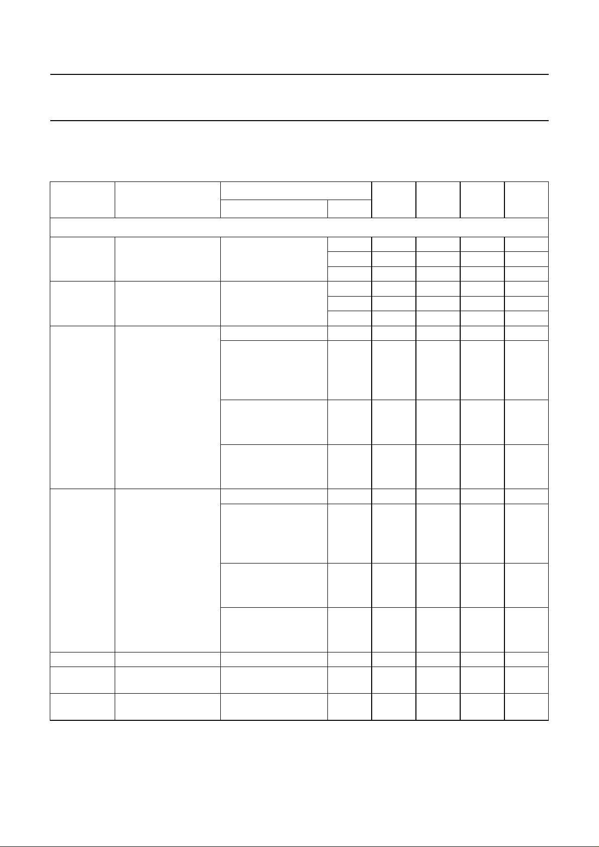
AC CHARACTERISTICS
Family 74HC
GND = 0 V; tr=tf= 6 ns; CL=50pF.
SYMBOL PARAMETER
T
=25°C
amb
t
PHL/tPLH
propagation delay
SH_CP to Q7’
propagation delay
ST_CP to Qn
t
PHL
propagation delay
MR to Q7’
t
PZH/tPZL
3-state output enable time
OE to Qn
t
PHZ/tPLZ
3-state output disable time
OE to Qn
t
W
shift clock pulse width
HIGH or LOW
storage clock pulse width
HIGH or LOW
master reset pulse width
LOW
t
su
set-up time DS to SH_CP see Fig.9 2.0 50 11 − ns
set-up time
SH_CP to ST_CP
t
h
hold time DS to SH_CP see Fig.9 2.0 +3 −6 − ns
TEST CONDITIONS
WAVEFORMS V
see Fig.7 2.0 − 52 160 ns
see Fig.8 2.0 − 55 175 ns
see Fig.10 2.0 − 47 175 ns
see Fig.11 2.0 − 47 150 ns
see Fig.11 2.0 − 41 150 ns
see Fig.7 2.0 75 17 − ns
see Fig.8 2.0 75 11 − ns
see Fig.10 2.0 75 17 − ns
see Fig.8 2.0 75 22 − ns
74HC595; 74HCT595
(V)
CC
4.5 − 19 32 ns
6.0 − 15 27 ns
4.5 − 20 35 ns
6.0 − 16 30 ns
4.5 − 17 35 ns
6.0 − 14 30 ns
4.5 − 17 30 ns
6.0 − 14 26 ns
4.5 − 15 30 ns
6.0 − 12 26 ns
4.5 15 6 − ns
6.0 13 5 − ns
4.5 15 4 − ns
6.0 13 3 − ns
4.5 15 6.0 − ns
6.0 13 5.0 − ns
4.5 10 4.0 − ns
6.0 9.0 3.0 − ns
4.5 15 8 − ns
6.0 13 7 − ns
4.5 +3 −2 − ns
6.0 +3 −2 − ns
MIN. TYP. MAX. UNIT
2003 Jun 25 13

Philips Semiconductors Product specification
8-bit serial-in, serial or parallel-out shift
register with output latches; 3-state
SYMBOL PARAMETER
t
rem
f
max
removal time MR to SH_CP see Fig.10 2.0 +50 −19 − ns
maximum clock
pulse frequency
SH_CP or ST_CP
T
= −40 to +85 °C
amb
t
PHL/tPLH
propagation delay
SH_CP to Q7’
propagation delay
ST_CP to An
t
PHL
propagation delay
MR to Q7’
t
PZH/tPZL
3-state output enable time
OE to Qn
t
PHZ/tPLZ
3-state output disable time
OE to Qn
t
W
shift clock pulse width
HIGH or LOW
storage clock pulse width
HIGH or LOW
master reset pulse width
LOW
t
su
set-up time DS to SH_CP see Fig.9 2.0 65 −−ns
set-up time
SH_CP to ST_CP
TEST CONDITIONS
WAVEFORMS V
see Figs 7 and 8 2.0 9 30 − MHz
see Fig.7 2.0 −−200 ns
see Fig.8 2.0 −−220 ns
see Fig.10 2.0 −−220 ns
see Fig.11 2.0 −−190 ns
see Fig.11 2.0 −−190 ns
see Fig.7 2.0 95 −−ns
see Fig.8 2.0 95 −−ns
see Fig.10 2.0 95 −−ns
see Fig.8 2.0 95 −−ns
74HC595; 74HCT595
(V)
CC
4.5 +10 −7 − ns
6.0 +9 −6 − ns
4.5 30 91 − MHz
6.0 35 108 − MHz
4.5 −−40 ns
6.0 −−34 ns
4.5 −−44 ns
6.0 −−37 ns
4.5 −−44 ns
6.0 −−37 ns
4.5 −−38 ns
6.0 −−33 ns
4.5 −−38 ns
6.0 −−33 ns
4.5 19 −−ns
6.0 16 −−ns
4.5 19 −−ns
6.0 16 −−ns
4.5 19 −−ns
6.0 16 −−ns
4.5 13 −−ns
6.0 11 −−ns
4.5 19 −−ns
6.0 16 −−ns
MIN. TYP. MAX. UNIT
2003 Jun 25 14

Philips Semiconductors Product specification
8-bit serial-in, serial or parallel-out shift
register with output latches; 3-state
SYMBOL PARAMETER
t
h
t
rem
f
max
hold time DS to SH_CP see Fig.9 2.0 3 −−ns
removal time MR to SH_CP see Fig.10 2.0 65 −−ns
maximum clock
pulse frequency
SH_CP or ST_CP
T
= −40 to +125 °C
amb
t
PHL/tPLH
propagation delay
SH_CP to Q7’
propagation delay
ST_CP to Qn
t
PHL
propagation delay
MR to Q7’
t
PZH/tPZL
3-state output enable time
OE to Qn
t
PHZ/tPLZ
3-state output disable time
OE to Qn
t
W
shift clock pulse width
HIGH or LOW
storage clock pulse width
HIGH or LOW
master reset pulse width
LOW
TEST CONDITIONS
WAVEFORMS V
see Figs 7 and 8 2.0 4.8 −−MHz
see Fig.7 2.0 −−240 ns
see Fig.8 2.0 −−265 ns
see Fig.10 2.0 −−265 ns
see Fig.11 2.0 −−225 ns
see Fig.11 2.0 −−225 ns
see Fig.7 2.0 110 −−ns
see Fig.8 2.0 110 −−ns
see Fig.10 2.0 110 −−ns
74HC595; 74HCT595
(V)
CC
4.5 3 −−ns
6.0 3 −−ns
4.5 13 −−ns
6.0 11 −−ns
4.5 24 −−MHz
6.0 28 −−MHz
4.5 −−48 ns
6.0 −−41 ns
4.5 −−53 ns
6.0 −−45 ns
4.5 −−53 ns
6.0 −−45 ns
4.5 −−45 ns
6.0 −−38 ns
4.5 −−45 ns
6.0 −−38 ns
4.5 22 −−ns
6.0 19 −−ns
4.5 22 −−ns
6.0 19 −−ns
4.5 22 −−ns
6.0 19 −−ns
MIN. TYP. MAX. UNIT
2003 Jun 25 15

Philips Semiconductors Product specification
8-bit serial-in, serial or parallel-out shift
register with output latches; 3-state
SYMBOL PARAMETER
t
su
t
h
t
rem
f
max
set-up time DS to SH_CP see Fig.9 2.0 75 −−ns
set-up time
SH_CP to ST_CP
hold time DS to SH_CP see Fig.9 2.0 3 −−ns
removal time MR to SH_CP see Fig.10 2.0 75 −−ns
maximum clock
pulse frequency
SH_CP or ST_CP
TEST CONDITIONS
WAVEFORMS V
see Fig.8 2.0 110 −−ns
see Figs 7 and 8 2.0 4 −−MHz
74HC595; 74HCT595
(V)
CC
4.5 15 −−ns
6.0 13 −−ns
4.5 22 −−ns
6.0 19 −−ns
4.5 3 −−ns
6.0 3 −−ns
4.5 15 −−ns
6.0 13 −−ns
4.5 20 −−MHz
6.0 24 −−MHz
MIN. TYP. MAX. UNIT
2003 Jun 25 16

Philips Semiconductors Product specification
8-bit serial-in, serial or parallel-out shift
register with output latches; 3-state
Family 74HCT
GND = 0 V; tr=tf= 6 ns; CL=50pF.
SYMBOL PARAMETER
T
=25°C
amb
t
PHL/tPLH
propagation delay
SH_CP to Q7’
propagation delay
ST_CP to Qn
t
PHL
propagation delay
MR to Q7’
t
PZH/tPZL
3-state output enable time
OE to Qn
t
PHZ/tPLZ
3-state output disable time
OE to Qn
t
W
shift clock pulse width
HIGH or LOW
storage clock pulse width
HIGH or LOW
master reset pulse width
LOW
t
su
set-up time DS to SH_CP see Fig.9 4.5 16 5 − ns
set-up time
SH_CP to ST_CP
t
t
h
rem
hold time DS to SH_CP see Fig.9 4.5 +3 −2 − ns
removal time
MR to SH_CP
f
max
maximum clock
pulse frequency
SH_CP or ST_CP
T
= −40 to +85 °C
amb
t
PHL/tPLH
propagation delay
SH_CP to Q7’
propagation delay
ST_CP to Qn
t
PHL
propagation delay
MR to Q7’
t
PZH/tPZL
3-state output enable time
OE to Qn
t
PHZ/tPLZ
3-state output disable time
OE to Qn
TEST CONDITIONS
WAVEFORMS V
see Fig.7 4.5 − 25 42 ns
see Fig.8 4.5 − 24 40 ns
see Fig.10 4.5 − 23 40 ns
see Fig.11 4.5 − 21 35 ns
see Fig.11 4.5 − 18 30 ns
see Fig.7 4.5 16 6 − ns
see Fig.8 4.5 16 5 − ns
see Fig.10 4.5 20 8 − ns
see Fig.8 4.5 16 8 − ns
see Fig.10 4.5 +10 −7 − ns
see Figs 7 and 8 4.5 30 52 − MHz
see Fig.7 4.5 −−53 ns
see Fig.8 4.5 −−50 ns
see Fig.10 4.5 −−50 ns
see Fig.11 4.5 −−44 ns
see Fig.11 4.5 −−38 ns
CC
74HC595; 74HCT595
MIN. TYP. MAX. UNIT
(V)
2003 Jun 25 17

Philips Semiconductors Product specification
8-bit serial-in, serial or parallel-out shift
register with output latches; 3-state
SYMBOL PARAMETER
t
W
shift clock pulse width
HIGH or LOW
storage clock pulse width
HIGH or LOW
master reset pulse width
LOW
t
su
set-up time DS to SH_CP see Fig.9 4.5 20 −−ns
set-up time
SH_CP to ST_CP
t
t
h
rem
hold time DS to SH_CP see Fig.9 4.5 3 −−ns
removal time
MR to SH_CP
f
max
maximum clock
pulse frequency
SH_CP or ST_CP
T
= −40 to +125 °C
amb
t
PHL/tPLH
propagation delay
SH_CP to Q7’
propagation delay
ST_CP to Qn
t
PHL
propagation delay
MR to Q7’
t
PZH/tPZL
3-state output enable time
OE to Qn
t
PHZ/tPLZ
3-state output disable time
OE to Qn
t
W
shift clock pulse width
HIGH or LOW
storage clock pulse width
HIGH or LOW
master reset pulse width
LOW
t
su
set-up time DS to SH_CP see Fig.9 4.5 24 −−ns
set-up time
SH_CP to ST_CP
t
t
h
rem
hold time DS to SH_CP see Fig.9 4.5 3 −−ns
removal time
MR to SH_CP
f
max
maximum clock
pulse frequency
SH_CP or ST_CP
TEST CONDITIONS
WAVEFORMS V
see Fig.7 4.5 20 −−ns
see Fig.8 4.5 20 −−ns
see Fig.10 4.5 25 −−ns
see Fig.8 4.5 20 −−ns
see Fig.10 4.5 13 −−ns
see Figs 7 and 8 4.5 24 −−MHz
see Fig.7 4.5 −−63 ns
see Fig.8 4.5 −−60 ns
see Fig.10 4.5 −−60 ns
see Fig.11 4.5 −−53 ns
see Fig.11 4.5 −−45 ns
see Fig.7 4.5 24 −−ns
see Fig.8 4.5 24 −−ns
see Fig.10 4.5 30 −−ns
see Fig.8 4.5 24 −−ns
see Fig.10 4.5 15 −−ns
see Figs 7 and 8 4.5 20 −−MHz
CC
74HC595; 74HCT595
MIN. TYP. MAX. UNIT
(V)
2003 Jun 25 18

Philips Semiconductors Product specification
8-bit serial-in, serial or parallel-out shift
register with output latches; 3-state
AC WAVEFORMS
PLH
1/f
t
W
handbook, full pagewidth
SH_CP input
74HC595: VM= 50%; VI= GND to VCC.
74HCT595: VM= 1.3 V; VI= GND to 3 V.
Q7' output
V
M
t
max
t
TLH
t
PHL
90%
10%
74HC595; 74HCT595
V
M
t
THL
MSA699
Fig.7 Waveforms showing the clock (SH_CP) to output (Q7’)propagation delays, theshift clock pulsewidth and
maximum shift clock frequency.
handbook, full pagewidth
SH_CP input
ST_CP input
Qn output
74HC595: VM= 50%; VI= GND to VCC.
74HCT595: VM= 1.3 V; VI= GND to 3 V.
V
M
t
su
V
M
t
W
t
PLH
V
M
1/f
max
t
PHL
MSA700
Fig.8 Waveforms showing the storage clock (ST_CP) to output (Qn) propagation delays, the storage clock
pulse width and the shift clock to storage clock set-up time.
2003 Jun 25 19

Philips Semiconductors Product specification
8-bit serial-in, serial or parallel-out shift
register with output latches; 3-state
handbook, full pagewidth
SH_CP input
DS input
Q7' output
74HC595: VM= 50%; VI= GND to VCC.
74HCT595: VM= 1.3 V; VI= GND to 3 V.
V
M
t
su
V
M
74HC595; 74HCT595
t
t
h
V
M
su
t
h
MLB196
The shaded areas indicate when the input is permitted to change for predictable output performance.
Fig.9 Waveforms showing the data set-up and hold times for the DS input.
handbook, full pagewidth
MR input
SH_CP input
Q7' output
V
M
t
rem
V
M
t
PHL
t
W
V
M
MLB197
74HC595: VM= 50%; VI= GND to VCC.
74HCT595: VM= 1.3 V; VI= GND to 3 V.
Fig.10 Waveforms showing the Master Reset (MR) pulse width, the master reset to output (Q7’) propagation
delay and the master reset to shift clock (SH_CP) removal time.
2003 Jun 25 20

Philips Semiconductors Product specification
8-bit serial-in, serial or parallel-out shift
register with output latches; 3-state
handbook, full pagewidth
OE input
10%
Qn output
LOW-to-OFF
OFF-to-LOW
Qn output
HIGH-to-OFF
OFF-to-HIGH
t
90%
V
M
t
outputs
enabled
r
PLZ
t
PHZ
10%
90%
outputs
disabled
t
PZL
t
t
f
PZH
74HC595; 74HCT595
V
M
V
M
outputs
enabled
MSA697
74HC595: VM= 50%; VI= GND to VCC.
74HCT595: VM= 1.3 V; VI= GND to 3 V.
Fig.11 Waveforms showing the 3-state enable and disable times for input OE.
handbook, full pagewidth
TEST SWITCH
t
PLH/tPHL
t
PLZ/tPZL
t
PHZ/tPZH
open
V
CC
GND
PULSE
GENERATOR
V
CC
V
I
Definitions for test circuit:
RL= Load resistor.
CL= Load capacitance including jig and probe capacitance.
RT= Termination resistance should be equal to the output impedance Zo of the pulse generator.
D.U.T
R
T
V
O
CL50 pF
RL = 1 kΩ
MGK563
V
CC
Fig.12 Test circuit for 3-state outputs.
2003 Jun 25 21

Philips Semiconductors Product specification
8-bit serial-in, serial or parallel-out shift
register with output latches; 3-state
PACKAGE OUTLINES
DIP16: plastic dual in-line package; 16 leads (300 mil)
D
seating plane
L
Z
16
e
b
74HC595; 74HCT595
SOT38-4
M
E
A
2
A
A
1
w M
b
1
b
2
9
c
(e )
1
M
H
pin 1 index
1
0 5 10 mm
DIMENSIONS (inch dimensions are derived from the original mm dimensions)
A
A
A
UNIT
max.
mm
inches
Note
1. Plastic or metal protrusions of 0.25 mm (0.01 inch) maximum per side are not included.
OUTLINE
VERSION
SOT38-4
12
min.
max.
IEC JEDEC JEITA
b
1.73
1.30
0.068
0.051
b
1
0.53
0.38
0.021
0.015
b
cD E e M
2
0.36
1.25
0.23
0.85
0.014
0.049
0.009
0.033
REFERENCES
scale
(1) (1)
19.50
18.55
0.77
0.73
8
6.48
6.20
0.26
0.24
E
(1)
Z
L
3.60
8.25
3.05
7.80
0.14
0.32
0.12
0.31
EUROPEAN
PROJECTION
M
E
10.0
0.39
0.33
e
1
H
8.3
w
max.
0.2542.54 7.62
ISSUE DATE
0.010.1 0.3
95-01-14
03-02-13
0.764.2 0.51 3.2
0.030.17 0.02 0.13
2003 Jun 25 22

Philips Semiconductors Product specification
8-bit serial-in, serial or parallel-out shift
register with output latches; 3-state
SO16: plastic small outline package; 16 leads; body width 3.9 mm
D
c
y
Z
16
9
74HC595; 74HCT595
SOT109-1
E
H
E
A
X
v M
A
pin 1 index
1
e
0 2.5 5 mm
DIMENSIONS (inch dimensions are derived from the original mm dimensions)
UNIT
mm
inches
Note
1. Plastic or metal protrusions of 0.15 mm (0.006 inch) maximum per side are not included.
A
max.
1.75
0.069
A1A2A
0.25
1.45
0.10
1.25
0.010
0.057
0.004
0.049
0.25
0.01
b
3
p
0.49
0.25
0.36
0.19
0.0100
0.019
0.0075
0.014
(1)E(1) (1)
cD
10.0
9.8
0.39
0.38
8
w M
b
p
scale
eHELLpQZywv θ
4.0
3.8
0.16
0.15
1.27
0.05
6.2
5.8
0.244
0.228
A
2
1.05
0.041
Q
A
1
detail X
1.0
0.7
0.4
0.6
0.028
0.039
0.020
0.016
(A )
L
p
L
0.25 0.1
0.25
0.01
0.01 0.004
A
3
θ
0.7
0.3
0.028
0.012
o
8
o
0
OUTLINE
VERSION
SOT109-1
IEC JEDEC JEITA
076E07 MS-012
REFERENCES
2003 Jun 25 23
EUROPEAN
PROJECTION
ISSUE DATE
99-12-27
03-02-19

Philips Semiconductors Product specification
8-bit serial-in, serial or parallel-out shift
register with output latches; 3-state
SSOP16: plastic shrink small outline package; 16 leads; body width 5.3 mm
D
c
y
Z
16
9
E
H
E
74HC595; 74HCT595
SOT338-1
A
X
v M
A
pin 1 index
1
e
DIMENSIONS (mm are the original dimensions)
UNIT A1A2A3b
mm
Note
1. Plastic or metal protrusions of 0.25 mm maximum per side are not included.
A
max.
2
0.21
0.05
1.80
1.65
0.25
p
0.38
0.25
8
b
p
cD
0.20
6.4
0.09
6.0
w M
0 2.5 5 mm
scale
(1)E(1)
eHELLpQZywv θ
5.4
0.65 1.25
5.2
7.9
7.6
Q
A
2
A
1
detail X
1.03
0.9
0.63
0.7
(A )
L
p
L
3
θ
0.130.2 0.1
A
(1)
1.00
0.55
o
8
o
0
OUTLINE
VERSION
SOT338-1
IEC JEDEC JEITA
REFERENCES
MO-150
2003 Jun 25 24
EUROPEAN
PROJECTION
ISSUE DATE
99-12-27
03-02-19

Philips Semiconductors Product specification
8-bit serial-in, serial or parallel-out shift
74HC595; 74HCT595
register with output latches; 3-state
TSSOP16: plastic thin shrink small outline package; 16 leads; body width 4.4 mm
E
H
E
16
D
c
y
Z
9
SOT403-1
A
X
v M
A
pin 1 index
18
w M
b
e
DIMENSIONS (mm are the original dimensions)
UNIT A
mm
Notes
1. Plastic or metal protrusions of 0.15 mm maximum per side are not included.
2. Plastic interlead protrusions of 0.25 mm maximum per side are not included.
A
max.
1.1
OUTLINE
VERSION
SOT403-1 MO-153
1
0.15
0.05
A2A3b
0.95
0.25
0.80
IEC JEDEC JEITA
p
0.30
0.19
p
0 2.5 5 mm
scale
(1)E(2) (1)
cD
0.2
5.1
0.1
4.9
REFERENCES
eHELLpQZywv θ
4.5
0.65
4.3
A
6.6
6.2
Q
(A )
2
A
1
L
p
L
detail X
0.75
0.4
0.50
0.3
EUROPEAN
PROJECTION
3
A
θ
0.13 0.10.21
0.40
0.06
ISSUE DATE
99-12-27
03-02-18
o
8
o
0
2003 Jun 25 25

Philips Semiconductors Product specification
8-bit serial-in, serial or parallel-out shift
74HC595; 74HCT595
register with output latches; 3-state
DHVQFN16: plastic dual in-line compatible thermal enhanced very thin quad flat package; no leads;
16 terminals; body 2.5 x 3.5 x 0.85 mm
A
D
terminal 1
index area
B
A
A
E
1
detail X
SOT763-1
c
terminal 1
index area
L
1
E
h
16
DIMENSIONS (mm are the original dimensions)
(1)
A
UNIT
mm
Note
1. Plastic or metal protrusions of 0.075 mm maximum per side are not included.
max.
A
0.05
0.00
1
e
27
15
c
b
0.30
0.2
0.18
e
1
b
10
D
h
0 2.5 5 mm
D
3.6
3.4
(1)
2.15
1.85
(1)
E
2.6
2.4
E
1.15
0.85
h
D
h
v
w
8
e
9
scale
0.51
e
2.5
C
y
X
w
0.1v0.05
y
1
C
ye
0.05 0.1
y
1
M
ACCB
M
L
1
0.5
0.3
OUTLINE
VERSION
SOT763-1 MO-241 - - -- - -
IEC JEDEC JEITA
REFERENCES
2003 Jun 25 26
EUROPEAN
PROJECTION
ISSUE DATE
02-10-17
03-01-27

Philips Semiconductors Product specification
8-bit serial-in, serial or parallel-out shift
74HC595; 74HCT595
register with output latches; 3-state
DATA SHEET STATUS
LEVEL
I Objective data Development This data sheet contains data from the objective specification for product
II Preliminary data Qualification This data sheet contains data from the preliminary specification.
III Product data Production This data sheet contains data from the product specification. Philips
Notes
1. Please consult the most recently issued data sheet before initiating or completing a design.
2. The product status of the device(s) described in this data sheet may have changed since this data sheet was
3. For data sheets describing multiple type numbers, the highest-level product status determines the data sheet status.
DATA SHEET
STATUS
published. The latest information is available on the Internet at URL http://www.semiconductors.philips.com.
(1)
PRODUCT
STATUS
(2)(3)
DEFINITION
development. Philips Semiconductors reserves the right to change the
specification in any manner without notice.
Supplementary data will be published at a later date. Philips
Semiconductors reserves the right to change the specification without
notice, in order to improve the design and supply the best possible
product.
Semiconductors reserves the right to make changes at any time in order
to improve the design, manufacturing and supply. Relevant changes will
be communicated via a Customer Product/Process Change Notification
(CPCN).
DEFINITIONS
Short-form specification The data in a short-form
specification is extracted from a full data sheet with the
same type number and title. For detailed information see
the relevant data sheet or data handbook.
Limiting values definition Limiting values given are in
accordance with the Absolute Maximum Rating System
(IEC 60134). Stress above one or more of the limiting
values may cause permanent damage to the device.
These are stress ratings only and operation of the device
atthese or at any otherconditionsabove those given inthe
Characteristics sections of the specification is not implied.
Exposure to limiting values for extended periods may
affect device reliability.
Application information Applications that are
described herein for any of these products are for
illustrative purposes only. Philips Semiconductors make
norepresentationorwarranty that such applications will be
suitable for the specified use without further testing or
modification.
DISCLAIMERS
Life support applications These products are not
designed for use in life support appliances, devices, or
systems where malfunction of these products can
reasonably be expected to result inpersonal injury. Philips
Semiconductorscustomersusingor selling these products
for use in such applications do so at their own risk and
agree to fully indemnify Philips Semiconductors for any
damages resulting from such application.
Right to make changes Philips Semiconductors
reserves the right to make changes in the products including circuits, standard cells, and/or software described or contained herein in order to improve design
and/or performance. Whenthe product is in full production
(status ‘Production’), relevant changes will be
communicated via a Customer Product/Process Change
Notification (CPCN). Philips Semiconductors assumes no
responsibility or liability for the use of any of these
products, conveys no licence or title under any patent,
copyright, or mask work right to these products, and
makes no representations or warranties that these
products are free from patent, copyright, or mask work
right infringement, unless otherwise specified.
2003 Jun 25 27

Philips Semiconductors – a w orldwide compan y
Contact information
For additional information please visit http://www.semiconductors.philips.com. Fax: +31 40 27 24825
For sales offices addresses send e-mail to: sales.addresses@www.semiconductors.philips.com.
© Koninklijke Philips Electronics N.V. 2003
All rights are reserved. Reproduction in whole or in part is prohibited without the prior written consent of the copyright owner.
The information presented in this document does not form part of any quotation or contract, is believed to be accurate and reliable and may be changed
without notice. No liability will be accepted by the publisher for any consequence of its use. Publication thereof does not convey nor imply any license
under patent- or other industrial or intellectual property rights.
Printed in The Netherlands 613508/04/pp28 Date of release: 2003 Jun 25 Document order number: 9397750 11263
SCA75
 Loading...