

Philips 74HCT4015D, 74HCT4015U, 74HCT4015N, 74HC4015U, 74HC4015N Datasheet
...
DATA SH EET
Product specification
File under Integrated Circuits, IC06
December 1990
INTEGRATED CIRCUITS
74HC/HCT4015
Dual 4-bit serial-in/parallel-out shift
register
For a complete data sheet, please also download:
•The IC06 74HC/HCT/HCU/HCMOS Logic Family Specifications
•The IC06 74HC/HCT/HCU/HCMOS Logic Package Information
•The IC06 74HC/HCT/HCU/HCMOS Logic Package Outlines

December 1990 2
Philips Semiconductors Product specification
Dual 4-bit serial-in/parallel-out shift
register
74HC/HCT4015
FEATURES
• Output capability: standard
• ICC category: MSI
GENERAL DESCRIPTION
The 74HC/HCT4015 are high-speed Si-gate CMOS
devices and are pin compatible with the “4015” of the
“4000B” series. They are specified in compliance with
JEDEC standard no. 7A.
The 74HC/HCT4015 are dual edge-triggered 4-bit static
shift registers (serial-to-parallel converters). Each shift
register has a serial data input (1D and 2D), a clock input
(1CP and 2CP), four fully buffered parallel outputs (1Q
0
to
1Q3 and 2Q0 to 2Q3) and an overriding asynchronous
master reset (1MR and 2MR). Information present on nD
is shifted to the first register position, and all data in the
register is shifted one position to the right on the
LOW-to-HIGH transition of nCP.
A HIGH on nMR clears the register and forces nQ0 to nQ
3
to LOW, independent of nCP and nD.
QUICK REFERENCE DATA
GND = 0 V; T
amb
=25°C; tr=tf= 6 ns
Notes
1. C
PD
is used to determine the dynamic power dissipation (PD in µW):
PD=CPD× V
CC
2
× fi+∑(CL× V
CC
2
× fo) where:
fi= input frequency in MHz
fo= output frequency in MHz
∑ (CL× V
CC
2
× fo) = sum of outputs
CL= output load capacitance in pF
VCC= supply voltage in V
2. For HC the condition is VI= GND to V
CC
For HCT the condition is VI= GND to VCC− 1.5 V
ORDERING INFORMATION
See
“74HC/HCT/HCU/HCMOS Logic Package Information”
.
SYMBOL PARAMETER CONDITIONS
TYPICAL
UNIT
HC HCT
t
PHL
/ t
PLH
propagation delay nCP to nQ
n
CL= 15 pF; VCC=5 V1618ns
f
max
maximum clock frequency 110 74 MHz
C
I
input capacitance 3.5 3.5 pF
C
PD
power dissipation capacitance per register notes 1 and 2 35 40 pF
December 1990 3
Philips Semiconductors Product specification
Dual 4-bit serial-in/parallel-out shift register 74HC/HCT4015
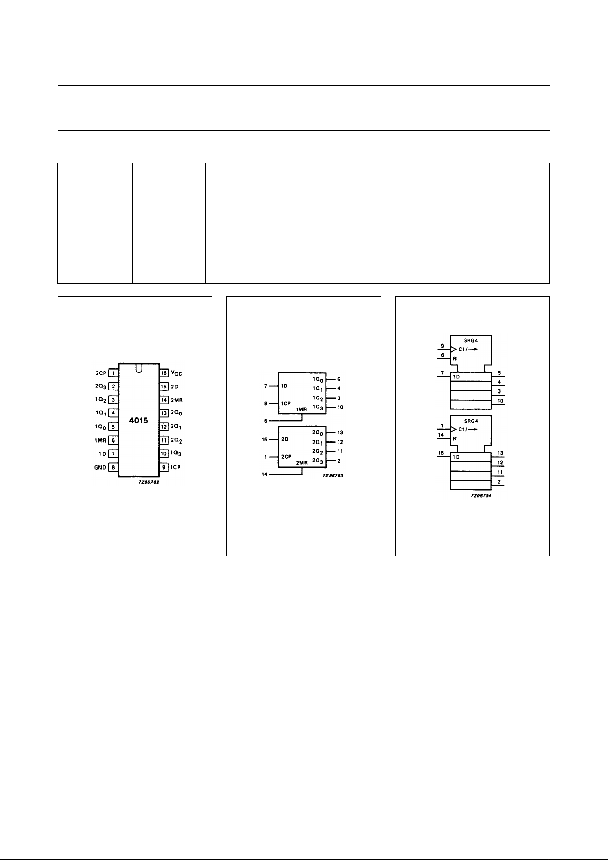
PIN DESCRIPTION
PIN NO. SYMBOL NAME AND FUNCTION
5, 4, 3, 10 1Q
0
to 1Q
3
flip-flop outputs
6, 14 1MR, 2MR asynchronous master reset inputs (active HIGH)
7, 15 1D, 2D serial data inputs
8 GND ground (0 V)
9, 1 1CP, 2CP clock inputs (LOW-to-HIGH, edge-triggered)
13, 12, 11, 2 2Q
0
to 2Q
3
flip-flop outputs
16 V
CC
positive supply voltage
Fig.1 Pin configuration. Fig.2 Logic symbol. Fig.3 IEC logic symbol.
 Loading...