

Philips 74HCT4060U, 74HCT4060DB, 74HCT4060D, 74HC4060DB, 74HC4060D Datasheet
...
DATA SH EET
Product specification
File under Integrated Circuits, IC06
December 1990
INTEGRATED CIRCUITS
74HC/HCT4060
14-stage binary ripple counter with
oscillator
For a complete data sheet, please also download:
•The IC06 74HC/HCT/HCU/HCMOS Logic Family Specifications
•The IC06 74HC/HCT/HCU/HCMOS Logic Package Information
•The IC06 74HC/HCT/HCU/HCMOS Logic Package Outlines
December 1990 2
Philips Semiconductors Product specification
14-stage binary ripple counter with oscillator 74HC/HCT4060
FEATURES
• All active components on chip
• RC or crystal oscillator configuration
• Output capability: standard (except for RTC and CTC)
• ICC category: MSI
GENERAL DESCRIPTION
The 74HC/HCT4060 are high-speed Si-gate CMOS
devices and are pin compatible with “4060” of the “4000B”
series. They are specified in compliance with JEDEC
standard no. 7A.
The 74HC/HCT4060 are 14-stage ripple-carry
counter/dividers and oscillators with three oscillator
terminals (RS, R
TC
and CTC), ten buffered outputs (Q3to
Q9and Q11to Q13) and an overriding asynchronous
master reset (MR).
The oscillator configuration allows design of either RC or
crystal oscillator circuits. The oscillator may be replaced by
an external clock signal at input RS. In this case keep the
other oscillator pins (RTCand CTC) floating.
The counter advances on the negative-going transition of
RS. A HIGH level on MR resets the counter (Q3to Q9and
Q11to Q13= LOW), independent of other input conditions.
In the HCT version, the MR input is TTL compatible, but
the RS input has CMOS input switching levels and can be
driven by a TTL output by using a pull-up resistor to VCC.
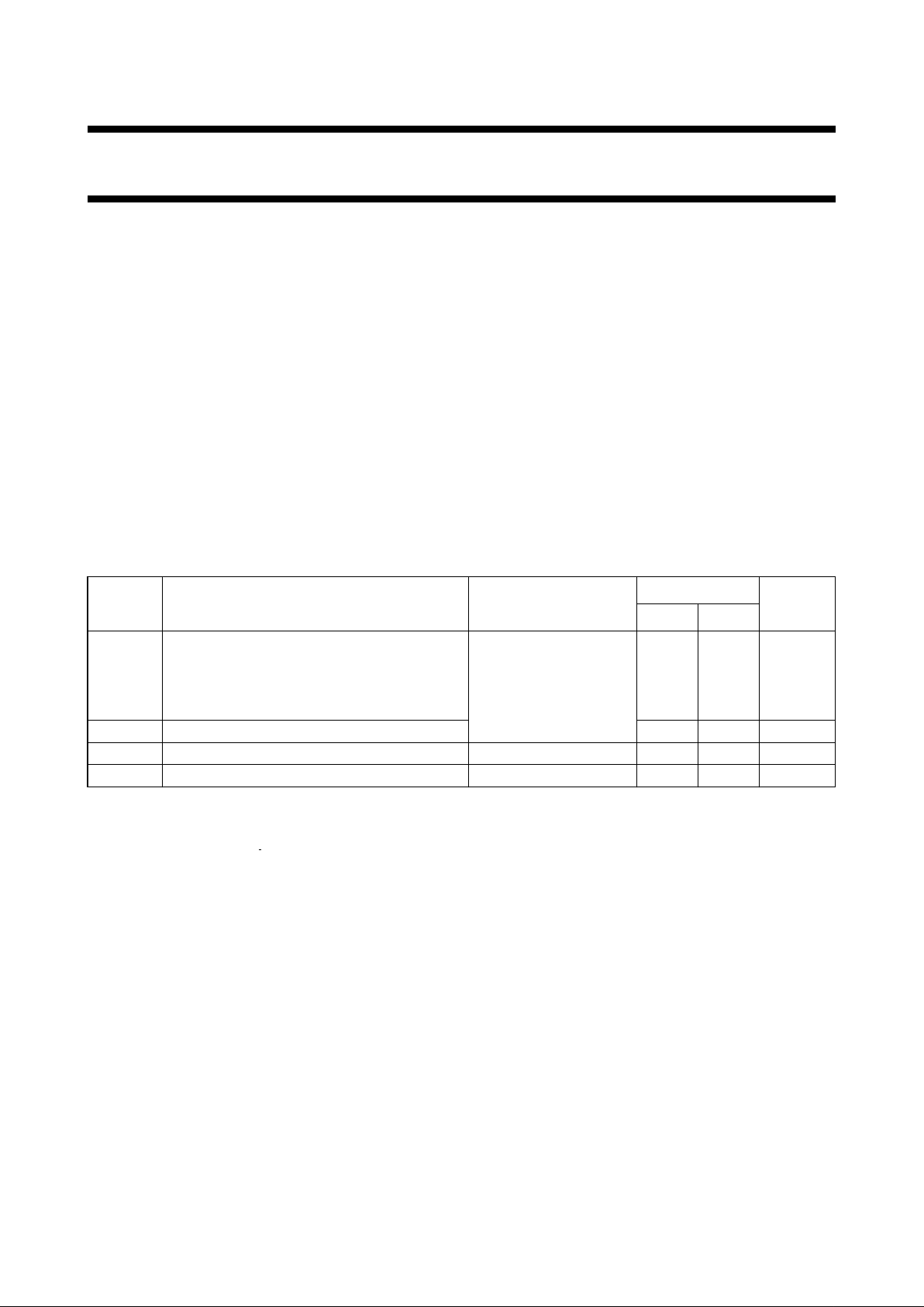
QUICK REFERENCE DATA
GND = 0 V; T
amb
=25°C; tr=tf= 6 ns
Notes
1. C
PD
is used to determine the dynamic power dissipation (PD in µW):
PD=CPD× V
CC
2
× fi+ ∑ (CL× V
CC
2
× fo) where:
fi= input frequency in MHz
fo= output frequency in MHz
∑ (CL× V
CC
2
× fo) = sum of outputs
CL= output load capacitance in pF
VCC= supply voltage in V
2. For HC the condition is VI= GND to V
CC
For HCT the condition is VI= GND to VCC− 1.5 V
3. For formula on dynamic power dissipation see next pages.
ORDERING INFORMATION
See
“74HC/HCT/HCU/HCMOS Logic Package Information”
.
SYMBOL PARAMETER CONDITIONS
TYPICAL
UNIT
HC HCT
t
PHL/ tPLH
propagation delay CL= 15 pF; VCC=5 V
RS to Q
3
31 31 ns
Q
n
to Q
n+1
66ns
t
PHL
MR to Q
n
17 18 ns
f
max
maximum clock frequency 87 88 MHz
C
I
input capacitance 3.5 3.5 pF
C
PD
power dissipation capacitance per package notes 1, 2 and 3 40 40 pF

December 1990 3
Philips Semiconductors Product specification
14-stage binary ripple counter with oscillator 74HC/HCT4060
PIN DESCRIPTION
PIN NO. SYMBOL NAME AND FUNCTION
1, 2, 3 Q
11
to Q
13
counter outputs
7, 5, 4, 6, 14, 13, 15 Q
3
to Q
9
counter outputs
8 GND ground (0 V)
9C
TC
external capacitor connection
10 R
TC
external resistor connection
11 RS clock input/oscillator pin
12 MR master reset
16 V
CC
positive supply voltage
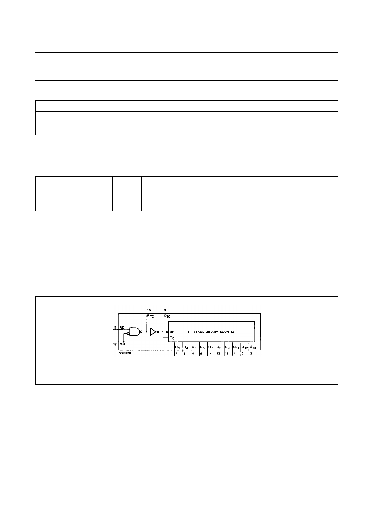
Fig.1 Pin configuration. Fig.2 Logic symbol. Fig.3 IEC logic symbol.
December 1990 4
Philips Semiconductors Product specification
14-stage binary ripple counter with oscillator 74HC/HCT4060
DYNAMIC POWER DISSIPATION FOR 74HC
Note
1. GND = 0 V; T
amb
=25°C
DYNAMIC POWER DISSIPATION FOR 74HCT
Notes
1. GND = 0 V; T
amb
=25°C
2. Where: fo= output frequency in MHz
f
osc
= oscillator frequency in MHz
∑ (CL× V
CC
2
× fo) = sum of outputs
CL= output load capacitance in pF
Ct= timing capacitance in pF
VCC= supply voltage in V
APPLICATIONS
• Control counters
• Timers
• Frequency dividers
• Time-delay circuits
PARAMETER V
CC
(V) TYPICAL FORMULA FOR PD(µW) (note 1)
total dynamic power
dissipation when using the
on-chip oscillator (P
D
)
2.0
4.5
6.0
CPD× f
osc
× V
CC
2
+∑(CL× V
CC
2
× fo) + 2Ct× V
CC
2
× f
osc
+ 60 × V
CC
CPD× f
osc
× V
CC
2
+∑(CL× V
CC
2
× fo) + 2Ct× V
CC
2
× f
osc
+ 1 750 × V
CC
CPD× f
osc
× V
CC
2
+∑(CL× V
CC
2
× fo) + 2Ct× V
CC
2
× f
osc
+ 3 800 × V
CC
PARAMETER VCC (V) TYPICAL FORMULA FOR PD(µW) (note 1)
total dynamic power
dissipation when using the
on-chip oscillator (P
D
)
4.5 CPD× f
osc
× V
CC
2
+∑(CL× V
CC
2
× fo) + 2Ct× V
CC
2
× f
osc
+ 1 750 × V
CC
Fig.4 Functional diagram.
 Loading...