

Philips 74HC4050U, 74HC4050N, 74HC4050DB, 74HC4050D Datasheet
DATA SH EET
Product specification
File under Integrated Circuits, IC06
December 1990
INTEGRATED CIRCUITS
74HC4050
Hex high-to-low level shifter
For a complete data sheet, please also download:
•The IC06 74HC/HCT/HCU/HCMOS Logic Family Specifications
•The IC06 74HC/HCT/HCU/HCMOS Logic Package Information
•The IC06 74HC/HCT/HCU/HCMOS Logic Package Outlines
December 1990 2
Philips Semiconductors Product specification
Hex high-to-low level shifter 74HC4050
FEATURES
• Output capability: standard
• ICC category: SSI
GENERAL DESCRIPTION
The 74HC4050 is a high-speed Si-gate CMOS device and
is pin compatible with the “4050” of the “4000B” series. It
is specified in compliance with JEDEC standard no. 7A.
The 74HC4050 provides six non-inverting buffers with a
modified input protection structure, which has no diode
connected to V
CC
. Input voltages of up to 15 V may
therefore be used. This feature enables the non-inverting
buffers to be used as logic level translators, which will
convert high level logic to low level logic, while operating
from a low voltage power supply. For example 15 V logic
(“4000B series”) can be converted down to 2 V logic.
The actual input switch level remains related to the V
CC
and is the same as mentioned in the family characteristics.
APPLICA TIONS
• Converting 15 V logic (“4000B” series) down to 2 V logic.
QUICK REFERENCE DATA
GND = 0 V; T
amb
=25°C; tr=tf= 6 ns
Notes
1. C
PD
is used to determine the dynamic power dissipation (PD in µW):
PD=CPD× V
CC
2
× fi+∑ (CL× V
CC
2
× fo) where:
fi= input frequency in MHz
fo= output frequency in MHz
CL= output load capacitance in pF
VCC= supply voltage in V
∑ (CL× V
CC
2
× fo) = sum of outputs
ORDERING INFORMATION
See
“74HC/HCT/HCU/HCMOS Logic Package Information”
.
SYMBOL PARAMETER CONDITIONS
TYPICAL
UNIT
HC
t
PHL
/ t
PLH
propagation delay nA to nY CL= 15 pF; VCC= 5 V 7 ns
C
I
input capacitance 3.5 pF
C
PD
power dissipation capacitance per buffer note 1 14 pF
December 1990 3
Philips Semiconductors Product specification
Hex high-to-low level shifter 74HC4050
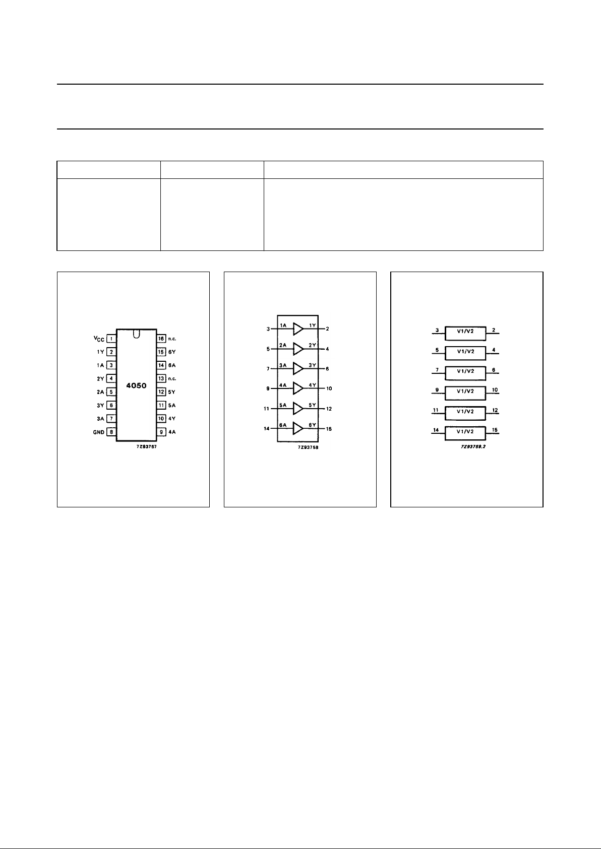
PIN DESCRIPTION
PIN NO. SYMBOL NAME AND FUNCTION
1V
CC
positive supply voltage
2, 4, 6, 10, 12, 15 1Y to 6Y data outputs
3, 5, 7, 9, 11, 14 1A to 6A data inputs
8 GND ground (0 V)
13, 16 n.c. not connected
Fig.1 Pin configuration.
Fig.2 Logic symbol. Fig.3 IEC logic symbol.
 Loading...