

Philips 74HCT40103U, 74HCT40103N, 74HCT40103DB, 74HCT40103D, 74HC40103D Datasheet
...
DATA SH EET
Product specification
Supersedes data of December 1990
File under Integrated Circuits, IC06
1998 Jul 08
INTEGRATED CIRCUITS
74HC/HCT40103
8-bit synchronous binary down
counter
For a complete data sheet, please also download:
•The IC06 74HC/HCT/HCU/HCMOS Logic Family Specifications
•The IC06 74HC/HCT/HCU/HCMOS Logic Package Information
•The IC06 74HC/HCT/HCU/HCMOS Logic Package Outlines
1998 Jul 08 2
Philips Semiconductors Product specification
8-bit synchronous binary down counter 74HC/HCT40103
FEATURES
• Cascadable
• Synchronous or asynchronous preset
• Output capability: standard
• ICCcategory: MSI
GENERAL DESCRIPTION
The 74HC/HCT40103 are high-speed Si-gate CMOS
devices and are pin compatible with the “40103” of the
“4000B” series. They are specified in compliance with
JEDEC standard no. 7A.
The 74HC/HCT40103 consist each of an 8-bit
synchronous down counter with a single output which is
active when the internal count is zero. The “40103”
contains a single 8-bit binary counter and has control
inputs for enabling or disabling the clock (CP), for clearing
the counter to its maximum count, and for presetting the
counter either synchronously or asynchronously. All
control inputs and the terminal count output (
TC) are
active-LOW logic.
In normal operation, the counter is decremented by one
count on each positive-going transition of the clock (CP).
Counting is inhibited when the terminal enable input (
TE)
is HIGH. The terminal count output (TC) goes LOW when
the count reaches zero ifTE is LOW, and remains LOW for
one full clock period.
When the synchronous preset enable input (PE) is LOW,
data at the jam input (P0to P7) is clocked into the counter
on the next positive-going clock transition regardless of the
state of TE. When the asynchronous preset enable input
(PL) is LOW, data at the jam input (P0to P7) is
asynchronously forced into the counter regardless of the
state of PE, TE, or CP. The jam inputs (P0to P7) represent
a single 8-bit binary word.
When the master reset input (MR) is LOW, the counter is
asynchronously cleared to its maximum count (decimal
255) regardless of the state of any other input. The
precedence relationship between control inputs is
indicated in the function table.
If all control inputs except TE are HIGH at the time of zero
count, the counters will jump to the maximum count, giving
a counting sequence of 256 clock pulses long.
The “40103” may be cascaded using the TE input and the
TC output, in either a synchronous or ripple mode.
QUICK REFERENCE DATA
GND = 0 V; T
amb
=25°C; tr=tf= 6 ns
Notes
1. C
PD
is used to determine the dynamic power dissipation (PDin µW):
PD=CPD× V
CC
2
× fi+∑(CL× V
CC
2
× fo) where:
fi= input frequency in MHz
fo= output frequency in MHz
∑ (CL× V
CC
2
× fo) = sum of outputs
CL= output load capacitance in pF
VCC= supply voltage in V
2. For HC the condition is VI= GND to V
CC
For HCT the condition is VI= GND to VCC− 1.5 V
SYMBOL PARAMETER CONDITIONS
TYPICAL
UNIT
HC HCT
t
PHL
/ t
PLH
propagation delay CP to TC CL= 15 pF; VCC= 5 V 30 30 ns
f
max
maximum clock frequency 32 31 MHz
C
I
input capacitance 3.5 3.5 pF
C
PD
power dissipation capacitance per package notes 1 and 2 24 27 pF
1998 Jul 08 3
Philips Semiconductors Product specification
8-bit synchronous binary down counter 74HC/HCT40103
ORDERING INFORMATION
PIN DESCRIPTION
TYPE NUMBER
PACKAGE
NAME DESCRIPTION VERSION
74HC40103N;
74HCT40103N
DIP16 plastic dual in-line package; 16 leads (300 mil); long body SOT38-1
74HC40103D;
74HCT40103D
SO16 plastic small outline package; 16 leads; body width 3.9 mm SOT109-1
74HC40103DB;
74HCT40103DB
SSOP16 plastic shrink small outline package; 16 leads; body width 5.3 mm SOT338-1
74HC40103PW; TSSOP16 plastic thin shrink small outline package; 16 leads; body width 4.4 mm SOT403-1
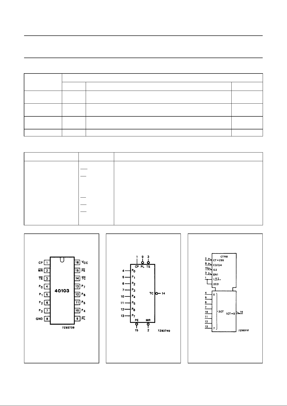
PIN NO. SYMBOL NAME AND FUNCTION
1 CP clock input (LOW-to-HIGH, edge-triggered)
2
MR asynchronous master reset input (active LOW)
3
TE terminal enable input
4, 5, 6, 7, 10, 11, 12, 13 P
0
to P
7
jam inputs
8 GND ground (0 V)
9
PL asynchronous preset enable input (active LOW)
14
TC terminal count output (active LOW)
15
PE synchronous preset enable input (active LOW)
16 V
CC
positive supply voltage
Fig.1 Pin configuration. Fig.2 Logic symbol. Fig.3 IEC logic symbol.
1998 Jul 08 4
Philips Semiconductors Product specification
8-bit synchronous binary down counter 74HC/HCT40103
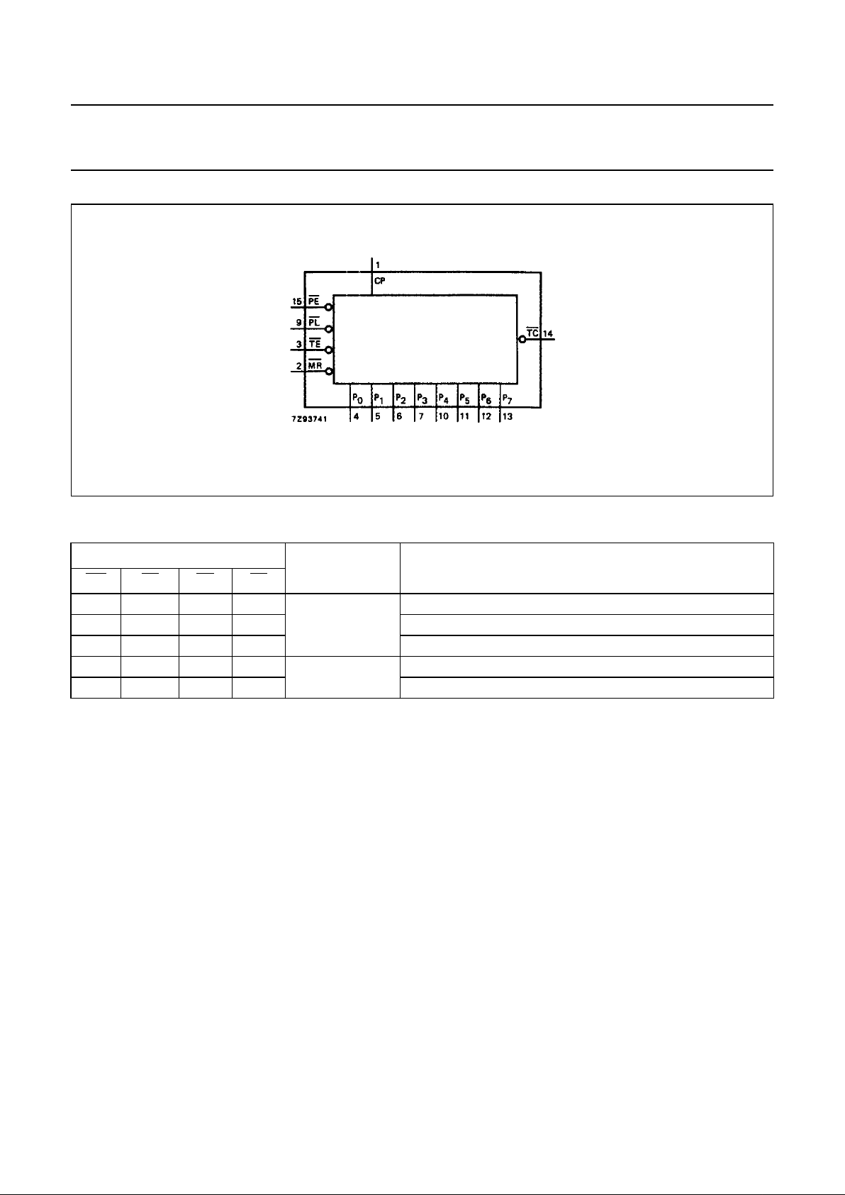
FUNCTION TABLE
Note
1. Clock connected to CP.
Synchronous operation: changes occur on the LOW-to-HIGH CP transition.
Jam inputs: MSD = P
7
, LSD = P0.
H = HIGH voltage level
L = LOW voltage level
X = don’t care
APPLICATIONS
• Divide-by-n counters
• Programmable timers
• Interrupt timers
• Cycle/program counters
CONTROL INPUTS
PRESET MODE ACTION
MR PL PE TE
HHHH
synchronous
inhibit counter
H H H L count down
H H L X preset on next LOW-to HIGH clock transition
HLXX
asynchronous
preset asynchronously
L X X X clear to maximum count
Fig.4 Functional diagram.
1998 Jul 08 5
Philips Semiconductors Product specification
8-bit synchronous binary down counter 74HC/HCT40103
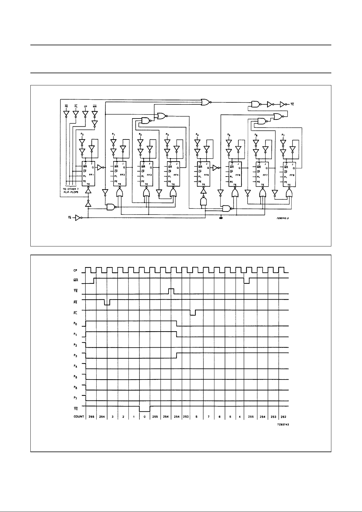
Fig.5 Logic diagram.
Fig.6 Timing diagram.
1998 Jul 08 6
Philips Semiconductors Product specification
8-bit synchronous binary down counter 74HC/HCT40103
DC CHARACTERISTICS FOR 74HC
For the DC characteristics see
“74HC/HCT/HCU/HCMOS Logic Family Specifications”
.
Output capability: standard
ICCcategory: MSI
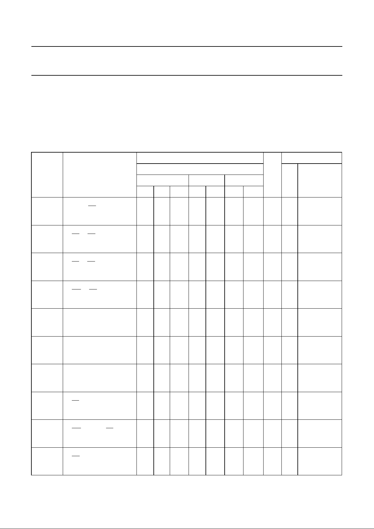
AC CHARACTERISTICS FOR 74HC
GND = 0 V; t
r=tf
= 6 ns; CL= 50 pF
SYMBOL PARAMETER
T
amb
(°C)
UNIT
TEST CONDITIONS
74HC
V
CC
(V)
WAVEFORMS
+25 −40 to +85 −40 to +125
min. typ. max. min. max. min. max.
t
PHL
/ t
PLH
propagation delay
CP to TC
96 300 375 450 ns 2.0 Fig.7
35 60 75 90 4.5
28 51 64 77 6.0
t
PHL
/ t
PLH
propagation delay
TE to TC
50 175 220 265 ns 2.0 Fig.8
18 35 44 53 4.5
14 30 37 45 6.0
t
PHL
/ t
PLH
propagation delay
PL to TC
102 315 395 475 ns 2.0 Fig.9
37 63 79 95 4.5
30 53 40 81 6.0
t
PHL
propagation delay
MR to TC
83 275 345 415 ns 2.0 Fig.9
30 55 69 83 4.5
24 47 59 71 6.0
t
THL
/ t
TLH
output transition time 19 75 95 110 ns 2.0 Figs 7 and 8
7 15 19 22 4.5
6 13 16 19 6.0
t
W
clock pulse width
HIGH or LOW
165 22 205 250 ns 2.0 Fig.7
33 8 41 50 4.5
28 6 35 43 6.0
t
W
master reset pulse width
LOW
125 39 155 190 ns 2.0 Fig.9
25 14 31 38 4.5
21 11 26 32 6.0
t
W
preset enable pulse width
PL; LOW
125 33 155 190 ns 2.0 Fig.9
25 12 31 38 4.5
21 10 26 32 6.0
t
rem
removal time
MR to CP or PL to CP
50 14 65 75 ns 2.0 Fig.10
10 5 13 15 4.5
9 4 11 13 6.0
t
su
set-up time
PE to CP
75 22 95 110 ns 2.0 Fig.11
15 8 19 22 4.5
13 6 16 19 6.0
 Loading...