

Philips 74ABT620PW, 74ABT620N, 74ABT620DB, 74ABT620D Datasheet

INTEGRATED CIRCUITS
74ABT620
Octal transceiver with dual enable,
inverting (3-State)
Product specification 1993 Jun 21
IC23 Data Handbook
Philips Semiconductors Product specification
Octal transceiver with dual enable, inverting
(3-State)
FEA TURES
•Octal bidirectional bus interface
•3-State buffers
•Power-up 3-State
•Live insertion/extraction permitted
•Output capability: +64mA/–32mA
•Latch-up protection exceeds 500mA per Jedec Std 17
•ESD protection exceeds 2000 V per MIL STD 883 Method 3015
and 200 V per Machine Model
QUICK REFERENCE DATA
SYMBOL PARAMETER
t
PLH
t
PHL
C
C
I
CCZ
IN
I/O
Propagation delay
An to Bn or Bn to An
Input capacitance
OEAB, OEBA
CL = 50pF; VCC = 5V 3.1 ns
VI = 0V or V
I/O capacitance Outputs disabled; V
Total supply current Outputs disabled; VCC = 5.5V 50 µA
DESCRIPTION
The 74ABT620 high-performance BiCMOS device combines low
static and dynamic power dissipation with high speed and high
output drive.
The 74ABT620 device is an octal transceiver featuring inverting
3-State bus compatible outputs in both send and receive directions.
The 74ABT620 is designed for asynchronous two-way
communication between data buses. The control function
implementation allows for maximum flexibility in timing. This device
allows data transmission from the A bus to the B bus or from the B
bus to the A bus, depending upon the logic levels at the Enable
inputs (OEBA
the device so that the buses are effectively isolated.
CONDITIONS
= 25°C; GND = 0V
T
amb
CC
O
74ABT620
and OEAB). The Enable inputs can be used to disable
TYPICAL UNIT
4 pF
= 0V or V
CC
7 pF
ORDERING INFORMATION
PACKAGES TEMPERATURE RANGE OUTSIDE NORTH AMERICA NORTH AMERICA DWG NUMBER
20-Pin Plastic DIP –40°C to +85°C 74ABT620 N 74ABT620 N SOT146-1
20-Pin plastic SO –40°C to +85°C 74ABT620 D 74ABT620 D SOT163-1
20-Pin Plastic SSOP Type II –40°C to +85°C 74ABT620 DB 74ABT620 DB SOT339-1
20-Pin Plastic TSSOP Type I –40°C to +85°C 74ABT620 PW 74ABT620PW DH SOT360-1
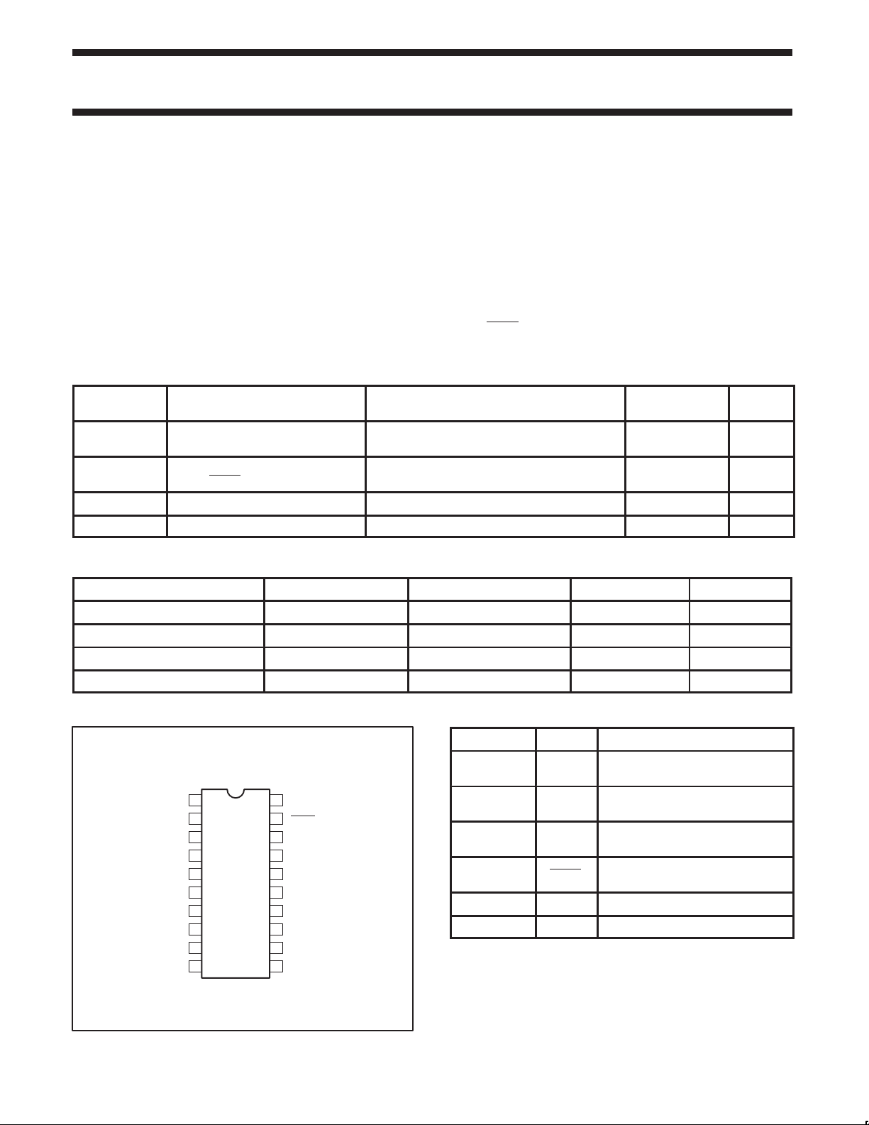
PIN CONFIGURATION
1
OEAB
2
A0
3
A1
4
A2
5
A3
6
A4
7
A5
8
A6
9
A7
10 11
GND
20
V
CC
19
OEBA
18
B0
17
B1
16
B2
15
B3
14
B4
13
B5
12
B6
B7
PIN DESCRIPTION
PIN NUMBER SYMBOL NAME AND FUNCTION
1 OEAB
2, 3, 4, 5,
6, 7, 8, 9
18, 17, 16, 15,
14, 13, 12, 11
A0 – A7 Data inputs/outputs (A side)
B0 – B7 Data inputs/outputs (B side)
19 OEBA
10 GND Ground (0V)
20 V
Output enable input, A side to B side
(active-High)
Output enable input, B side to A side
(active-Low)
Positive supply voltage
CC
SA00189
1993 Jun 21 853–161 1 10081
2

Philips Semiconductors Product specification
Octal transceiver with dual enable, inverting
(3-State)
LOGIC SYMBOL
OEAB
1
2
A0
3
A1
4
A2
5
A3
6
A4
7
A5
8
A6
9
A7
19
OEBA
18
B0
17
B1
16
B2
15
B3
14
B4
13
B5
12
B6
11
B7
SA00190
LOGIC SYMBOL (IEEE/IEC)
1
19
2
3
4
5
6
7
8
9
EN1
EN1
1
74ABT620
18
2
17
16
15
14
13
12
11
SA00191
FUNCTION TABLE
INPUTS INPUTS/OUTPUTS
OEBA OEAB An Bn
L L Bn Inputs
H H Inputs An
H L ZZ
Bn Inputs
L H
H =High voltage level
L =Low voltage level
Z =High impedance ”off” state
ABSOLUTE MAXIMUM RA TINGS
SYMBOL
V
V
I
CC
I
IK
V
I
OK
OUT
OUT
T
stg
DC supply voltage –0.5 to +7.0 V
DC input diode current VI < 0 –18 mA
DC input voltage
I
DC output diode current VO < 0 –50 mA
DC output voltage
DC output current output in Low state 128 mA
Storage temperature range –65 to 150 °C
NOTES:
1. Stresses beyond those listed may cause permanent damage to the device. These are stress ratings only and functional operation of the
device at these or any other conditions beyond those indicated under “recommended operating conditions” is not implied. Exposure to
absolute-maximum-rated conditions for extended periods may affect device reliability .
2. The performance capability of a high-performance integrated circuit in conjunction with its thermal environment can create junction
temperatures which are detrimental to reliability. The maximum junction temperature of this integrated circuit should not exceed 150°C.
3. The input and output voltage ratings may be exceeded if the input and output current ratings are observed.
PARAMETER CONDITIONS RATING UNIT
3
3
or
Inputs A
1, 2
n
–1.2 to +7.0 V
output in Off or High state –0.5 to +5.5 V
1993 Jun 21
3

Philips Semiconductors Product specification
Octal transceiver with dual enable, inverting
(3-State)
RECOMMENDED OPERATING CONDITIONS
SYMBOL PARAMETER LIMITS UNIT
Min Max
V
CC
V
V
V
I
OH
I
OL
∆t/∆v Input transition rise or fall rate 0 5 ns/V
T
amb
DC ELECTRICAL CHARACTERISTICS
SYMBOL PARAMETER TEST CONDITIONS T
V
IK
V
OH
V
OL
I
I
OFF
I
PU/IPD
IIH + I
IIL + I
I
CEX
I
O
I
CCH
I
CCL
I
CCZ
∆I
CC
NOTES:
1. Not more than one output should be tested at a time, and the duration of the test should not exceed one second.
2. This is the increase in supply current for each input at 3.4V.
3. This parameter is valid for any V
transition time of up to 100µsec is permitted.
DC supply voltage 4.5 5.5 V
Input voltage 0 V
I
High-level input voltage 2.0 V
IH
Low-level Input voltage 0.8 V
IL
High-level output current –32 mA
Low-level output current 64 mA
Operating free-air temperature range –40 +85 °C
LIMITS
= +25°C
amb
Min Typ Max Min Max
Input clamp voltage VCC = 4.5V; IIK = –18mA –0.9 –1.2 –1.2 V
VCC = 4.5V; IOH = –3mA; VI = VIL or V
High-level output voltage VCC = 5.0V; IOH = –3mA; VI = VIL or V
VCC = 4.5V; IOH = –32mA; VI = VIL or V
Low-level output voltage VCC = 4.5V; IOL = 64mA; VI = VIL or V
Input leakage Control pins VCC = 5.5V; VI = GND or 5.5V ±0.01 ±1.0 ±1.0 µA
I
IH
IH
IH
IH
2.5 2.9 2.5 V
3.0 3.4 3.0 V
2.0 2.4 2.0 V
0.42 0.55 0.55 V
current Data pins VCC = 5.5V; VI = GND or 5.5V ±5 ±100 ±100 µA
Power-off leakage current VCC = 0.0V; VO or VI ≤ 4.5V ±5.0 ±100 ±100 µA
Power-up/down 3-State
output current
3-State output High current VCC = 5.5V; VO = 2.7V; VI = VIL or V
OZH
3-State output Low current VCC = 5.5V; VO = 0.5V; VI = VIL or V
OZL
3
Output High leakage current VCC = 5.5V; VO = 5.5V; VI = GND or V
Output current
1
Quiescent supply current VCC = 5.5V; Outputs Low, VI = GND or V
Additional supply current per
input pin
2
CC
VCC = 2.1V; VO = 0.5V; VI = GND or VCC;
and VOE = Don’t care
V
OE
IH
IH
CC
±5.0 ±50 ±50 µA
5.0 50 50 µA
–5.0 –50 –50 µA
5.0 50 50 µA
VCC = 5.5V; VO = 2.5V –50 –100 –180 –50 –180 mA
VCC = 5.5V; Outputs High, VI = GND or V
VCC = 5.5V; Outputs 3-State;
= GND or V
V
I
CC
VCC = 5.5V; one input at 3.4V,
other inputs at V
or GND
CC
CC
CC
50 250 250 µA
24 30 30 mA
50 250 250 µA
0.05 1.5 1.5 mA
between 0V and 2.1V , with a transition time of up to 10msec. From VCC = 2.1V to VCC = 5V ± 10% a
74ABT620
CC
T
= –40°C
amb
to +85°C
V
UNIT
1993 Jun 21
4
 Loading...