

Philips 74ABT573AN, 74ABT573ADB, 74ABT573AD, 74ABT573APW Datasheet
Philips Semiconductors Product specification
Octal D-type transparent latch (3-State)
FEA TURES
•74ABT573A is flow-through pinout version of 74ABT373
•Inputs and outputs on opposite side of package allow easy
interface to microprocessors
•3-State output buffers
•Common output enable
•Latch-up protection exceeds 500mA per JEDEC Std 17
•ESD protection exceeds 2000 V per MIL STD 883 Method 3015
and 200 V per Machine Model
•Power-up 3-State
•Power-up reset
DESCRIPTION
The 74ABT573A high-performance BiCMOS device combines low
static and dynamic power dissipation with high speed and high
output drive.
QUICK REFERENCE DAT A
SYMBOL PARAMETER
C
t
PLH
t
PHL
C
OUT
I
CCZ
IN
Propagation delay
Dn to Qn
CL = 50pF; VCC = 5V
Input capacitance VI = 0V or V
Output capacitance Outputs disabled; VO = 0V or V
Total supply current Outputs disabled; VCC =5.5V 100 µA
74ABT573A
The 74ABT573A device is an octal transparent latch coupled to
eight 3-State output buffers. The two sections of the device are
controlled independently by Enable (E) and Output Enable (OE
control gates. The 74ABT573A is functionally identical to the
74ABT373 but has a flow-through pinout configuration to facilitate
PC board layout and allow easy interface with microprocessors.
The data on the D inputs are transferred to the latch outputs when
the Latch Enable (E) input is High. The latch remains transparent to
the data inputs while E is High, and stores the data that is present
one setup time before the High-to-Low enable transition.
The 3-State output buffers are designed to drive heavily loaded
3-State buses, MOS memories, or MOS microprocessors. The
active-Low Output Enable (OE
independent of the latch operation.
When OE
outputs. When OE
is Low, the latched or transparent data appears at the
is High, the outputs are in the High-impedance
”OFF” state, which means they will neither drive nor load the bus.
CONDITIONS
= 25°C; GND = 0V
T
amb
CC
CC
) controls all eight 3-State buffers
TYPICAL UNIT
2.8
3.3
3 pF
6 pF
)
ns
ORDERING INFORMATION
PACKAGES TEMPERATURE RANGE OUTSIDE NORTH AMERICA NORTH AMERICA DWG NUMBER
20-Pin Plastic DIP –40°C to +85°C 74ABT573A N 74ABT573A N SOT146-1
20-Pin plastic SO –40°C to +85°C 74ABT573A D 74ABT573A D SOT163-1
20-Pin Plastic SSOP Type II –40°C to +85°C 74ABT573A DB 74ABT573A DB SOT339-1
20-Pin Plastic TSSOP Type I –40°C to +85°C 74ABT573A PW 74ABT573APW DH SOT360-1
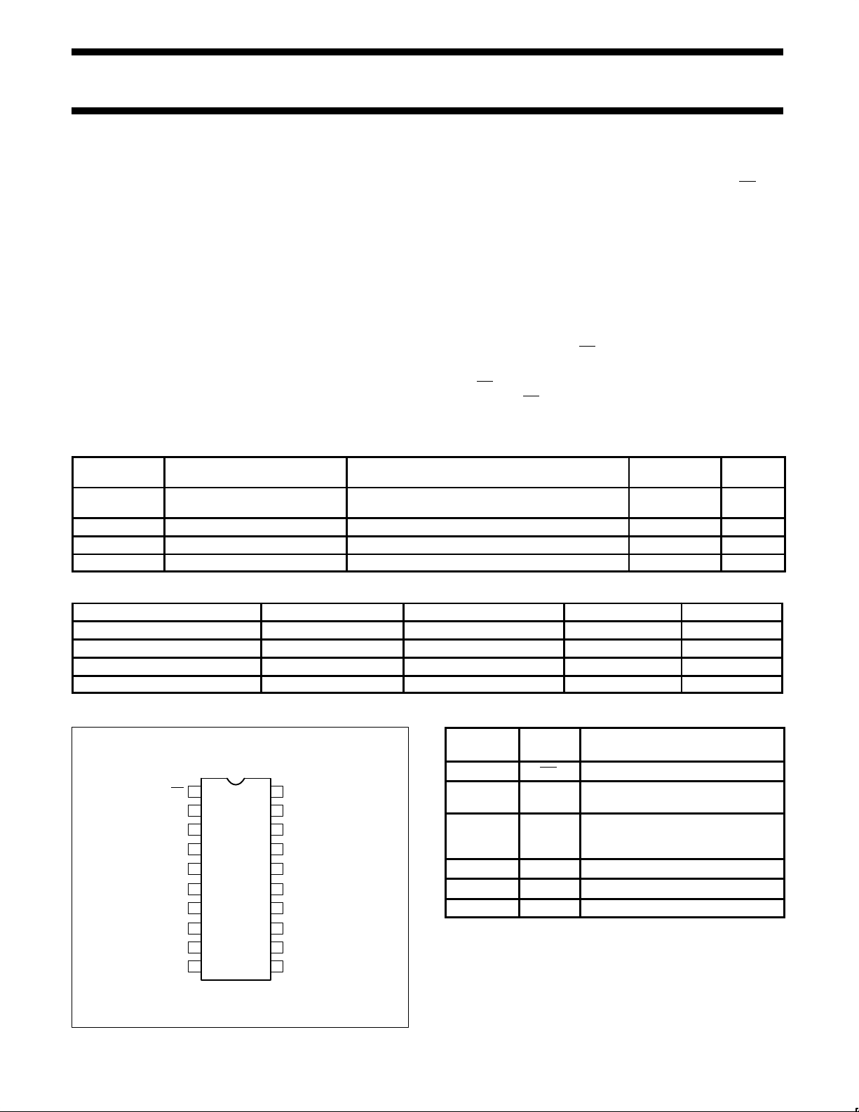
PIN CONFIGURA TION
1
OE
2
D0
3
D1
4
D2
5
D3
D4
6
D5
7
D6
8
D7
9
GND
10 11
20
V
CC
19
Q0
18
Q1
17
Q2
16
Q3
15
Q4
14
Q5
13
Q6
12
Q7
E
PIN DESCRIPTION
PIN
NUMBER
1 OE Output enable input (active-Low)
2, 3, 4, 5,
6, 7, 8, 9
19, 18, 17,
16, 15, 14,
13, 12
11 E Enable input (active-High)
10 GND Ground (0V)
20 V
SYMBOL FUNCTION
D0-D7 Data inputs
Q0-Q7 Data outputs
Positive supply voltage
CC
SA00185
1995 Sep 06 853–1455 15703
1
Philips Semiconductors Product specification
Octal D-type transparent latch (3-State)
LOGIC SYMBOL (IEEE/IEC)
1
EN
11
C1
2
2D 1
3
4
5
6
7
8
9
FUNCTION TABLE
INPUTS INTERNAL OUTPUTS OPERATING MODE
OE E Dn REGISTER Q0 – Q7
L
L
L
L
L L X NC NC Hold
H
H
H = High voltage level
h = High voltage level one set-up time prior to the High-to-Low E transition
L = Low voltage level
l = Low voltage level one set-up time prior to the High-to-Low E transition
NC= No change
X = Don’t care
Z = High impedance “off” state
↓ = High-to-Low E transition
H
H
↓
↓
L
H
Dn
L
H
l
h
X
NC
Dn
19
18
17
16
15
14
13
12
SA00187
L
H
L
H
L
H
L
H
Z
Z
Enable and read register
Latch and read register
Disable outputs
LOGIC SYMBOL
11
E
1
OE
74ABT573A
23456789
D0 D1 D2 D3 D4 D5 D6 D7
Q0 Q1 Q2 Q3 Q4 Q5 Q6 Q7
19 18 17 16 15 14 13 12
SA00186
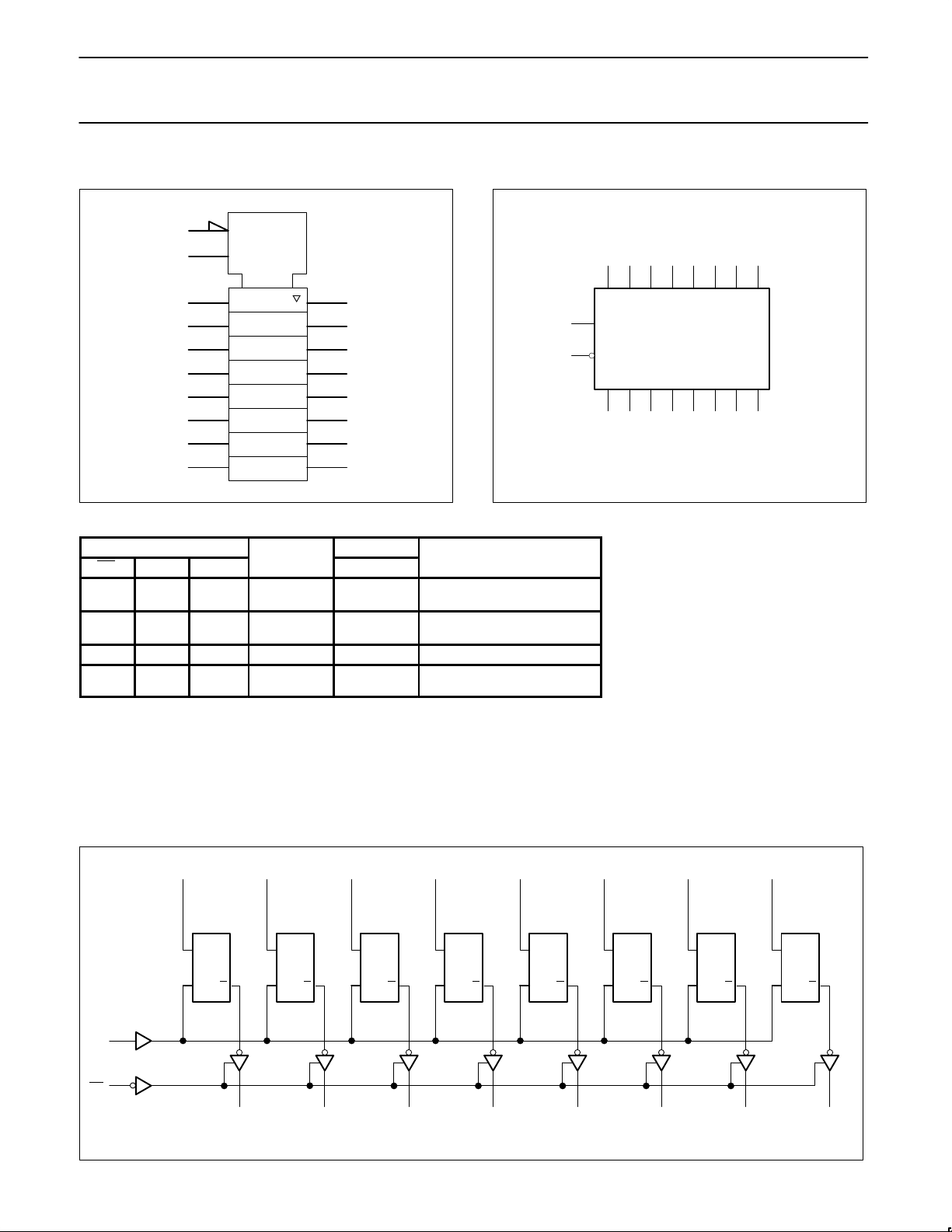
LOGIC DIAGRAM
D0
2
11
E
1
OE
1995 Sep 06
D
EQ
Q0
D1
3
D
EQ
19
Q1
D2
4
D
EQ
18
Q2
D3
5
D
EQ
17
Q3
D4
6
D
EQ
16
Q4
D5
7
D
EQ
15
Q5
D6
8
D
EQ
14
Q6
D7
9
D
EQ
13
12
Q7
SA00188
2
 Loading...