

Philips 74abt543a DATASHEETS

INTEGRATED CIRCUITS
74ABT543A
Octal latched transceiver
with dual enable (3-State)
Product specification
Supersedes data of 1995 Apr 19
IC23 Data Handbook
1998 Sep 24

Philips Semiconductors Product specification
Octal latched transceiver with dual enable
(3-State)
FEA TURES
•Combines 74ABT245 and 74ABT373 type functions in one device
•8-bit octal transceiver with D-type latch
•Back-to-back registers for storage
•Separate controls for data flow in each direction
•Output capability: +64mA/–32mA
•Live insertion/extraction permitted
•Power-up 3-State
•Power-up reset
•Latch-up protection exceeds 500mA per Jedec Std 17
•ESD protection exceeds 2000 V per MIL STD 883 Method 3015
and 200 V per Machine Model
DESCRIPTION
The 74ABT543A high-performance BiCMOS device combines low
static and dynamic power dissipation with high speed and high
output drive.
QUICK REFERENCE DATA
SYMBOL PARAMETER
t
PLH
t
PHL
C
C
I
CCZ
IN
I/O
Propagation delay
An to Bn or Bn to An
CL = 50pF; VCC = 5V
Input capacitance VI = 0V or V
I/O capacitance
Outputs disabled;
V
= 0V or V
O
Total supply current Outputs disabled; VCC =5.5V 110 µA
74ABT543A
The 74ABT543A Octal Registered Transceiver contains two sets of
D-type latches for temporary storage of data flowing in either
direction. Separate Latch Enable (LEAB
, OEBA) inputs are provided for each register to permit
(OEAB
independent control of data transfer in either direction. The outputs
are guaranteed to sink 64mA.
FUNCTIONAL DESCRIPTION
The 74ABT543A contains two sets of eight D-type latches, with
separate control pins for each set. Using data flow from A to B as an
example, when the A-to-B Enable (EAB
Enable (LEAB
subsequent Low-to-High transition of the LEAB
data into the latches where it is stored and the B outputs no longer
change with the A inputs. With EAB
3-State B output buffers are active and display the data present at
the outputs of the A latches.
Control of data flow from B to A is similar, but using the EBA
and OEBA
CONDITIONS
T
= 25°C; GND = 0V
amb
CC
CC
) input are Low the A-to-B path is transparent. A
inputs.
, LEBA) and Output Enable
) input and the A-to-B Latch
signal puts the A
and OEAB both Low, the
TYPICAL UNIT
2.9
3.6
4 pF
7 pF
, LEBA,
ns
ORDERING INFORMATION
PACKAGES TEMPERATURE RANGE OUTSIDE NORTH AMERICA NORTH AMERICA DWG NUMBER
24-Pin Plastic DIP –40°C to +85°C 74ABT543A N 74ABT543A N SOT222-1
24-Pin plastic SO –40°C to +85°C 74ABT543A D 74ABT543A D SOT137-1
24-Pin Plastic SSOP Type II –40°C to +85°C 74ABT543A DB 74ABT543A DB SOT340-1
24-Pin Plastic TSSOP Type I –40°C to +85°C 74ABT543A PW 7ABT543APW DH SOT355-1
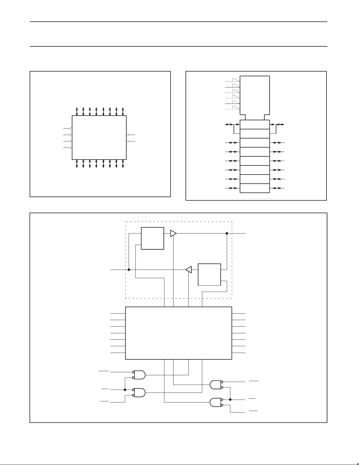
PIN CONFIGURATION
1
LEBA
2
OEBA
3
A0
4
A1
5
A2
6
A3
7
A4
8
A5
9
A6
10 15
A7
11
EAB
GND
12 13
24
V
CC
23
EBA
22
B0
21
B1
20
B2
19
B3
18
B4
17
B5
16
B6
B7
14
LEAB
OEAB
SA00168
PIN DESCRIPTION
PIN NUMBER SYMBOL FUNCTION
14, 1 LEAB / LEBA
11, 23 EAB / EBA
13, 2 OEAB / OEBA
3, 4, 5, 6,
7, 8, 9, 10
22, 21, 20, 19,
18, 17, 16, 15
A0 – A7 Port A, 3-State outputs
B0 – B7 Port B, 3-State outputs
12 GND Ground (0V)
24 V
CC
A to B / B to A Latch Enable
input (active-Low)
A to B / B to A Enable input
(active-Low)
A to B / B to A Output Enable
input (active-Low)
Positive supply voltage
1998 Sep 24 853-1794 20080
2
Philips Semiconductors Product specification
Octal latched transceiver with dual enable
(3-State)
LOGIC SYMBOL
3456
A0 A1 A2 A3
11
EAB
23
EBA
14 LEAB
1 LEBA
B0 B1 B2
2122
78910
A4 A5 A6 A7
B4 B5 B6
B3
1718
1920
13OEAB
2OEBA
B7
1516
SA00169
LOGIC SYMBOL (IEEE/IEC)
2
23
1
13
22
24
3
421
520
619
718
817
916
10 15
1EN3
G1
1C5
2EN4
G2
2C6
∇ 3
6D
(BA)
(AB)
74ABT543A
22
5D
2 ∇
SA00170
LOGIC DIAGRAM
OEBA
EBA
LEBA
DETAIL A
D
Q
LE
3
A0
4
A1
5
A2
6
A3
7
A4
8
A5
9
A6
10
A7
2
23
1
DETAIL A X 7
D
Q
LE
22
B0
21
B1
20
B2
19
B3
18
B4
17
B5
16
B6
15
B7
13
OEAB
11
EAB
14
LEAB
SA00171
1998 Sep 24
3
Philips Semiconductors Product specification
Octal latched transceiver with dual enable
(3-State)
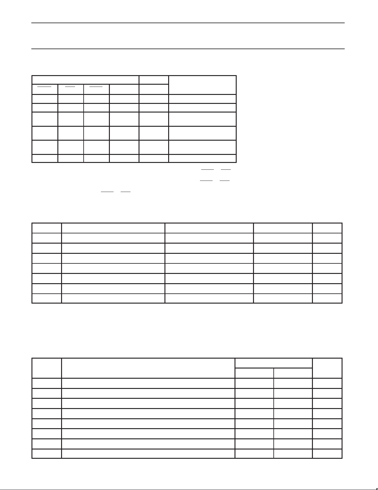
FUNCTION TABLE
INPUTS OUTPUTS STATUS
OEXX EXX LEXX An or Bn Bn or An
H X X X Z Disabled
X H X X Z Disabled
L
L
L
L
L
L
L L H X NC Hold
H = High voltage level
h = High voltage level one set-up time prior to the Low-to-High transition of LEXX
L = Low voltage level
l = Low voltage level one set-up time prior to the Low-to-High transition of LEXX
X = Don’t care
↑ = Low-to-High transition of LEXX
NC= No change
Z = High impedance or “off” state
↑
↑
L
L
L
L
L
L
↑
↑
L
L
h
l
h
l
H
L
Z
Z
H
L
H
L
Disabled + Latch
Latch + Display
Transparent
or EXX (XX = AB or BA)
74ABT543A
or EXX (XX = AB or BA)
or EXX (XX = AB or BA)
ABSOLUTE MAXIMUM RATINGS
SYMBOL
V
CC
I
IK
V
I
I
OK
V
OUT
I
OUT
T
stg
DC supply voltage –0.5 to +7.0 V
DC input diode current VI < 0 –18 mA
DC input voltage
DC output diode current VO < 0 –50 mA
DC output voltage
DC output current output in Low state 128 mA
Storage temperature range –65 to 150 °C
PARAMETER CONDITIONS RATING UNIT
3
3
1, 2
–1.2 to +7.0 V
output in Off or High state –0.5 to +5.5 V
NOTES:
1. Stresses beyond those listed may cause permanent damage to the device. These are stress ratings only and functional operation of the
device at these or any other conditions beyond those indicated under “recommended operating conditions” is not implied. Exposure to
absolute-maximum-rated conditions for extended periods may affect device reliability .
2. The performance capability of a high-performance integrated circuit in conjunction with its thermal environment can create ju nction
temperatures which are detrimental to reliability. The maximum junction temperature of this integrated circuit should not exceed 150°C.
3. The input and output voltage ratings may be exceeded if the input and output current ratings are observed.
RECOMMENDED OPERATING CONDITIONS
SYMBOL PARAMETER LIMITS UNIT
Min Max
V
CC
V
V
V
I
OH
I
OL
∆t/∆v Input transition rise or fall rate 0 10 ns/V
T
amb
DC supply voltage 4.5 5.5 V
Input voltage 0 V
I
High-level input voltage 2.0 V
IH
Low-level input voltage 0.8 V
IL
High-level output current –32 mA
Low-level output current 64 mA
Operating free-air temperature range –40 +85 °C
CC
V
1998 Sep 24
4
 Loading...