

Philips 74ABT541PW, 74ABT541DB, 74ABT541D Datasheet

74ABT541
Octal buffer/line driver (3-State)
Product specification
Supersedes data of 1996 Sep 10
1998 Jan 16
INTEGRATED CIRCUITS
IC23 Data Handbook

Philips Semiconductors Product specification
74ABT541Octal buffer/line driver (3-State)
2
1998 Jan 16 853-1458 18864
FEA TURES
•Octal bus interface
•Functions similar to the ’ABT241
•Provides ideal interface and increases fan-out of MOS
Microprocessors
•Efficient pinout to facilitate PC board layout
•3-State buffer outputs sink 64mA and source 32mA
•Power-up 3-State
•Latch-up protection exceeds 500mA per Jedec JC40.2 Std 17
•ESD protection exceeds 2000 V per MIL STD 883 Method 3015
and 200 V per Machine Model
•Live insertion/extraction permitted
DESCRIPTION
The 74ABT541 high-performance BiCMOS device combines low
static and dynamic power dissipation with high speed and high
output drive.
The 74ABT541 device is an octal buffer that is ideal for driving bus
lines. The outputs are all capable of sinking 64mA and sourcing
32mA. The device features input and outputs on opposite sides of
the package to facilitate printed circuit board layout.
QUICK REFERENCE DA TA
SYMBOL PARAMETER
CONDITIONS
T
amb
= 25°C; GND = 0V
TYPICAL UNIT
t
PLH
t
PHL
Propagation delay
An to Yn
CL = 50pF; VCC = 5V 2.9 ns
C
IN
Input capacitance VI = 0V or V
CC
4 pF
C
OUT
Output capacitance Outputs disabled; VO = 0V or V
CC
7 pF
I
CCZ
Total supply current Outputs disabled; VCC = 5.5V 500 nA
ORDERING INFORMATION
PACKAGES TEMPERATURE RANGE OUTSIDE NORTH AMERICA NORTH AMERICA DWG NUMBER
20-Pin Plastic DIP –40°C to +85°C 74ABT541 N 74ABT541 N SOT146-1
20-Pin plastic SO –40°C to +85°C 74ABT541 D 74ABT541 D SOT163-1
20-Pin Plastic SSOP Type II –40°C to +85°C 74ABT541 DB 74ABT541 DB SOT339-1
20-Pin Plastic TSSOP Type I –40°C to +85°C 74ABT541 PW 74ABT541PW DH SOT360-1
PIN CONFIGURATION
1
2
3
4
5
6
7
8
9
10 11
12
13
14
15
16
17
18
19
20
OE0
A0
A1
A2
A3
A4
A5
A6
A7
GND
V
CC
OE1
Y0
Y1
Y2
Y3
Y4
Y5
Y6
Y7
SA00202
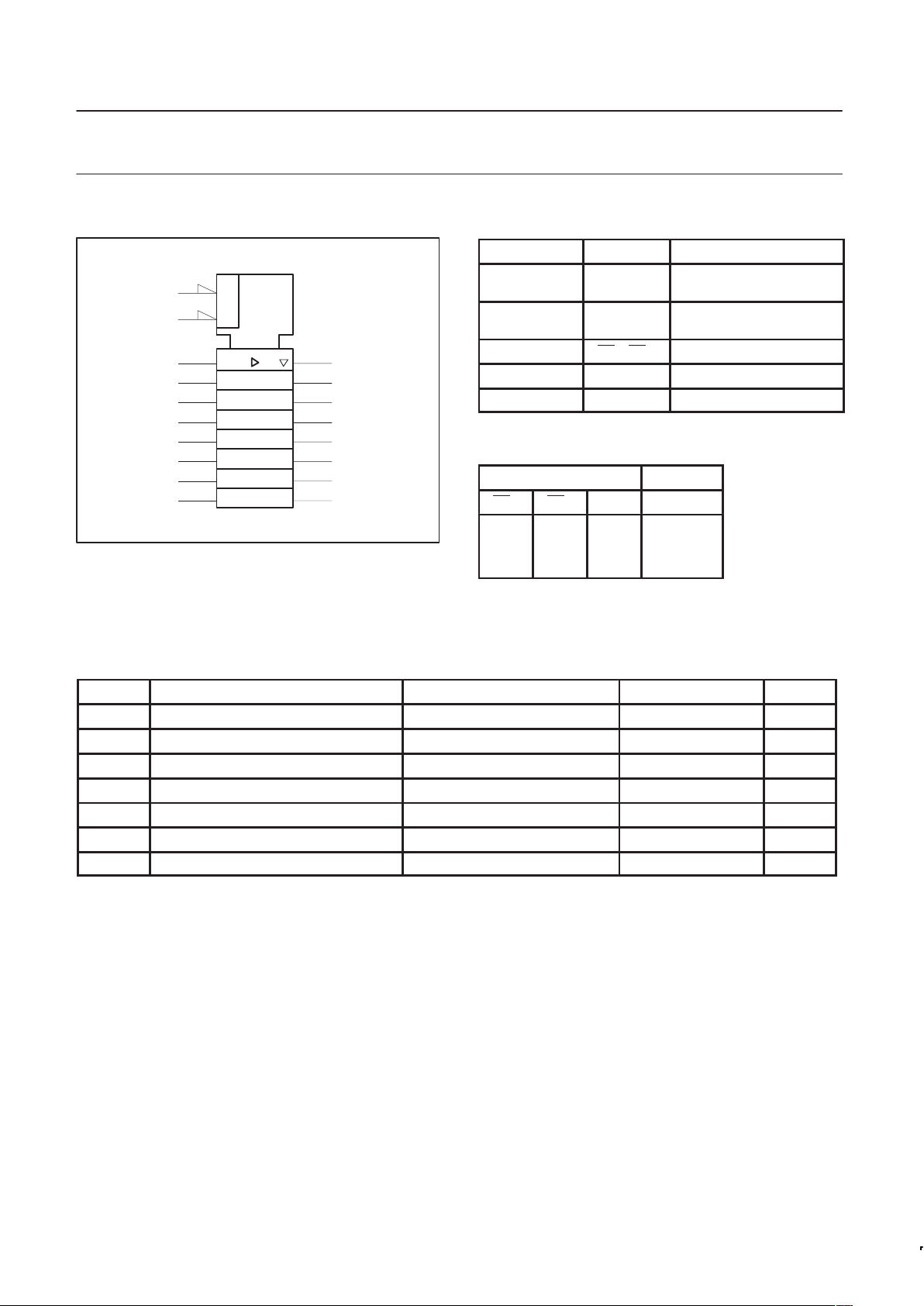
LOGIC SYMBOL
A0
A1
A2
A3
A4
A5
A6
A7
Y0
Y1
Y2
Y3
Y4
Y5
Y6
Y7
2
3
4
5
6
7
8
9
18
17
16
15
14
13
12
11
1
19
OE
0
OE
1
SA00203
Philips Semiconductors Product specification
74ABT541Octal buffer/line driver (3-State)
1998 Jan 16
3
LOGIC SYMBOL (IEEE/IEC)
EN
19
2 18
3
17
416
5
15
1
&
614
713
8
12
911
SA00204
PIN DESCRIPTION
PIN NUMBER SYMBOL NAME AND FUNCTION
2, 3, 4, 5,
6, 7, 8, 9
A0 – A7 Data inputs
18, 17, 16, 15,
14, 13, 12, 11
Y0 – Y7 Data outputs
1, 19 OE0, OE1 Output enables
10 GND Ground (0V)
20 V
CC
Positive supply voltage
FUNCTION TABLE
INPUTS OUTPUTS
OE0 OE1 An Yn
L
L
X
H
L
L
H
X
L
H
X
X
L
H
Z
Z
H =High voltage level
L =Low voltage level
X = Don’t care
Z =High impedance ”off” state
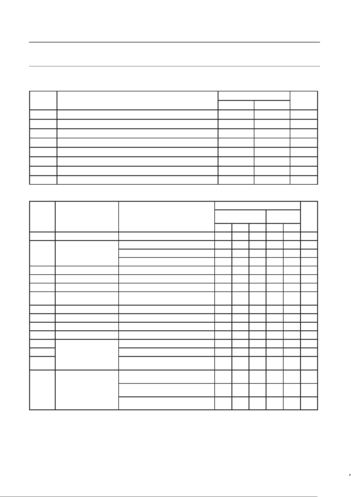
ABSOLUTE MAXIMUM RATINGS
1, 2
SYMBOL
PARAMETER CONDITIONS RATING UNIT
V
CC
DC supply voltage –0.5 to +7.0 V
I
IK
DC input diode current VI < 0 –18 mA
V
I
DC input voltage
3
–1.2 to +7.0 V
I
OK
DC output diode current VO < 0 –50 mA
V
OUT
DC output voltage
3
output in Off or High state –0.5 to +5.5 V
I
OUT
DC output current output in Low state 128 mA
T
stg
Storage temperature range –65 to 150 °C
NOTES:
1. Stresses beyond those listed may cause permanent damage to the device. These are stress ratings only and functional operation of the
device at these or any other conditions beyond those indicated under “recommended operating conditions” is not implied. Exposure to
absolute-maximum-rated conditions for extended periods may affect device reliability .
2. The performance capability of a high-performance integrated circuit in conjunction with its thermal environment can create junction
temperatures which are detrimental to reliability. The maximum junction temperature of this integrated circuit should not exceed 150°C.
3. The input and output voltage ratings may be exceeded if the input and output current ratings are observed.
Philips Semiconductors Product specification
74ABT541Octal buffer/line driver (3-State)
1998 Jan 16
4
RECOMMENDED OPERATING CONDITIONS
SYMBOL PARAMETER LIMITS UNIT
Min Max
V
CC
DC supply voltage 4.5 5.5 V
V
I
Input voltage 0 V
CC
V
V
IH
High-level input voltage 2.0 V
V
IL
Low-level Input voltage 0.8 V
I
OH
High-level output current –32 mA
I
OL
Low-level output current 64 mA
∆t/∆v Input transition rise or fall rate 0 5 ns/V
T
amb
Operating free-air temperature range –40 +85 °C
DC ELECTRICAL CHARACTERISTICS
LIMITS
SYMBOL PARAMETER TEST CONDITIONS T
amb
= +25°C
T
amb
= –40°C
to +85°C
UNIT
Min Typ Max Min Max
V
IK
Input clamp voltage VCC = 4.5V; IIK = –18mA –0.9 –1.2 –1.2 V
VCC = 4.5V; IOH = –3mA; VI = VIL or V
IH
2.5 2.9 2.5 V
V
OH
High-level output voltage VCC = 5.0V; IOH = –3mA; VI = VIL or V
IH
3.0 3.4 3.0 V
VCC = 4.5V; IOH = –32mA; VI = VIL or V
IH
2.0 2.4 2.0 V
V
OL
Low-level output voltage VCC = 4.5V; IOL = 64mA; VI = VIL or V
IH
0.42 0.55 0.55 V
I
I
Input leakage current VCC = 5.5V; VI = GND or 5.5V ±0.01 ±1.0 ±1.0 µA
I
OFF
Power-off leakage current VCC = 0.0V; VI or VO ≤ 4.5V ±5.0 ±100 ±100 µA
IPU/I
PD
Power-up/down 3-state
output current
3
VCC = 2.0V; VO = 0.5V; VI = GND or VCC;
VOE = Don’t care
±5.0 ±50 ±50 µA
I
OZH
3-State output High current VCC = 5.5V; VO = 2.7V; VI = VIL or V
IH
5.0 50 50 µA
I
OZL
3-State output Low current VCC = 5.5V; VO = 0.5V; VI = VIL or V
IH
–5.0 –50 –50 µA
I
CEX
Output High leakage current VCC = 5.5V; VO = 5.5V; VI = GND or V
CC
5.0 50 50 µA
I
O
Output current
1
VCC = 5.5V; VO = 2.5V –40 –100 –180 –40 –180 mA
I
CCH
VCC = 5.5V; Outputs High, VI = GND or V
CC
0.5 250 250 µA
I
CCL
Quiescent supply current VCC = 5.5V; Outputs Low , VI = GND or V
CC
24 30 30 mA
I
CCZ
VCC = 5.5V; Outputs 3-State;
VI = GND or V
CC
0.5 250 250 µA
Outputs enabled, one input at 3.4V , other
inputs at VCC or GND; VCC = 5.5V
0.5 1.5 1.5 mA
∆I
CC
Additional supply current per
input pin
2
Outputs 3-State, one data input at 3.4V ,
other inputs at VCC or GND; VCC = 5.5V
0.5 50 50 µA
Outputs 3-State, one enable input at 3.4V ,
other inputs at VCC or GND; VCC = 5.5V
0.5 1.5 1.5 mA
NOTES:
1. Not more than one output should be tested at a time, and the duration of the test should not exceed one second.
2. This is the increase in supply current for each input at 3.4V.
3. This parameter is valid for any VCC between 0V and 2.1V with a transition time of up to 10msec. For VCC = 2.1V to VCC = 5V 10%, a
transition time of up to 100µsec is permitted.
 Loading...