

Philips 74ABTH16899DGG, 74ABTH16899DL, 74ABT16899DL, 74ABT16899DGG Datasheet
INTEGRATED CIRCUITS
74ABT16899
74ABTH16899
18-bit latched transceiver with 16-bit
parity generator/checker (3-State)
Product specification
Supersedes data of 1997 Mar 28
IC23 Data Handbook
1998 Feb 25
Philips Semiconductors Product specification
Quiescent supply current
18-bit latched transceiver with 16-bit
parity generator/checker (3-State)
FEA TURES
•Symmetrical (A and B bus functions are identical)
•Selectable generate parity or ”feed-through” parity for A-to-B and
B-to-A directions
•Independent transparent latches for A-to-B and B-to-A directions
•Selectable ODD/EVEN parity
•Continuously checks parity of both A bus and B bus latches as
and ERRB
ERRA
•Open-collector ERR output
•Ability to simultaneously generate and check parity
•Can simultaneously read/latch A and B bus data
•Output capability: +64 mA/–32mA
•Latch-up protection exceeds 500mA per Jedec Std 17
•ESD protection exceeds 2000 V per MIL STD 883 Method 3015
and 200 V per Machine Model
•Power up 3-State
•Power-up reset
•Live insertion/extraction permitted
•Bus-hold data inputs eliminate the need for external pull-up
resistors to hold unused inputs
DESCRIPTION
The 74ABT/H16899 is a 16-bit to 16-bit parity transceiver with
separate transparent latches for the A bus and B bus. Either bus
can generate or check parity. The parity bit can be fed-through with
no change or the generated parity can be substituted with the SEL
input.
74ABT16899
74ABTH16899
Parity error checking of the A and B bus latches is continuously
provided with ERRA
The 74ABT/H16899 features independent latch enables for the A
and B bus latches, a select pin for ODD/EVEN
error signal output pins for checking parity.
FUNCTIONAL DESCRIPTION
The 74ABT/H16899 has three principal modes of operation which
are outlined below. All modes apply to both the A-to-B and B-to-A
directions.
Transparent latch, Generate parity, Check A and B bus parity:
Bus A (B) communicates to Bus B (A), parity is generated and
passed on to the B (A) Bus as BPAR (APAR). If LEA and LEB are
High and the Mode Select (SEL
A0-A7 and B0-B7 can be checked and monitored by ERRA
ERRB
. (Fault detection on both input and output buses.)
Transparent latch, Feed-through parity, Check A and B bus
parity:
Bus A (B) communicates to Bus B (A) in a feed-through mode if SEL
is High. Parity is still generated and checked as ERRA and ERRB
and can be used as an interrupt to signal a data/parity bit error to the
CPU.
Latched input, Generate/Feed-through parity, Check A (and B)
bus parity:
Independent latch enables (LEA and LEB) allow other permutations
of:
•Transparent latch / 1 bus latched / both buses latched
•Feed-through parity / generate parity
•Check in bus parity / check out bus parity / check in and out bus
parity
and ERRB, even with both buses in 3-State.
parity, and separate
) is Low, the parity generated from
and
QUICK REFERENCE DATA
SYMBOL PARAMETER
t
PLH
t
PHL
t
PLH
t
PHL
C
IN
C
I/O
I
CCZ
I
CCL
ORDERING INFORMATION
56-Pin Plastic SSOP Type III –40°C to +85°C 74ABT16899 DL BT16899 DL SOT371-1
56-Pin Plastic TSSOP Type II –40°C to +85°C 74ABT16899 DGG BT16899 DGG SOT364-1
56-Pin Plastic SSOP Type III –40°C to +85°C 74ABTH16899 DL BH16899 DL SOT371-1
56-Pin Plastic TSSOP Type II –40°C to +85°C 74ABTH16899 DGG BH16899 DGG SOT364-1
1998 Feb 25 853-1960 19018
CONDITIONS
T
= 25°C; GND = 0V
amb
Propagation delay
An to Bn or Bn to An
Propagation delay
An to ERRA
Input capacitance VI = 0V or V
Output capacitance Outputs disabled; VO = 0V or V
pp
PACKAGES TEMPERATURE RANGE OUTSIDE NORTH AMERICA NORTH AMERICA DWG NUMBER
CL = 50pF; VCC = 5V 2.7 ns
CL = 50pF; VCC = 5V 5.0 ns
CC
CC
Outputs disabled; VCC =5.5V 500 µA
Output Low; VCC = 5.5V 10.5 mA
2
TYPICAL UNIT
4 pF
7 pF
Philips Semiconductors Product specification
18-bit latched transceiver with 16-bit
parity generator/checker (3-State)
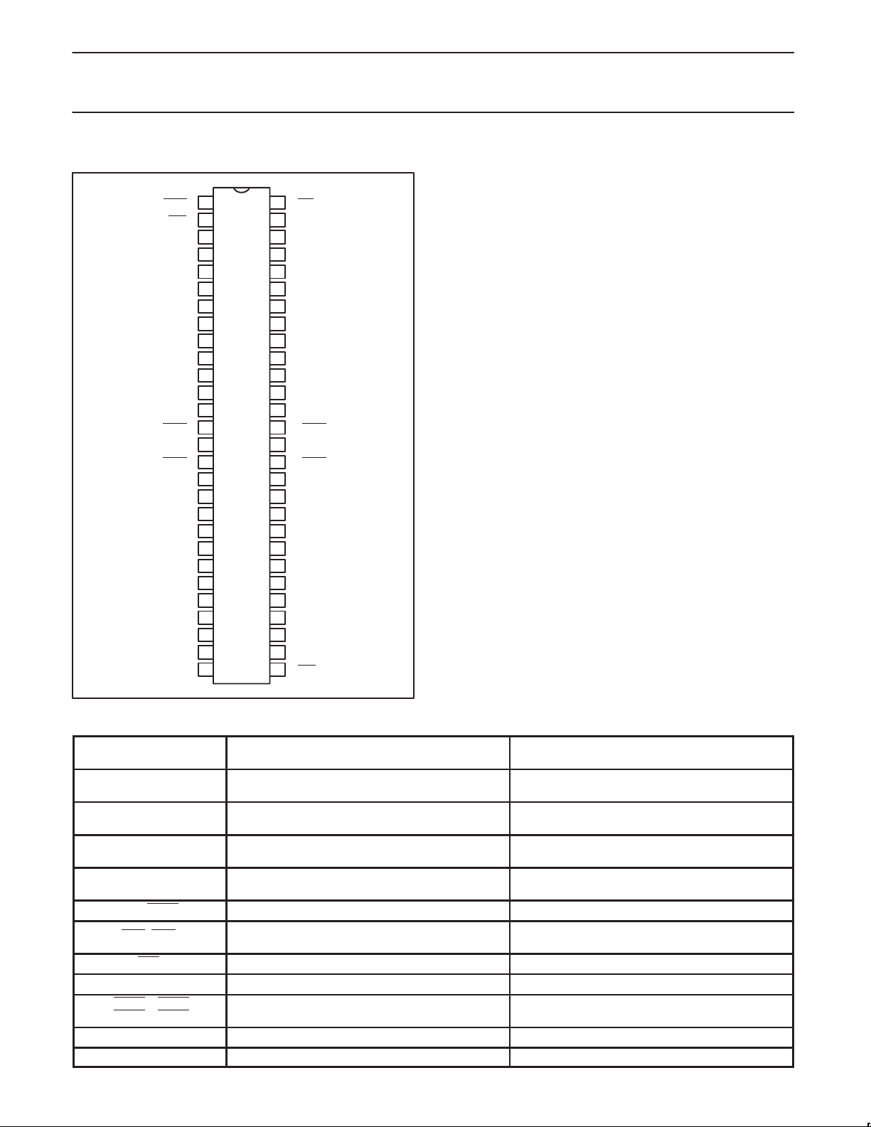
PIN CONFIGURATION
ODD/EVEN
1APAR
1ERRA
2ERRA
2APAR
1
2
OEA
3
1A0
4
GND
5
1A1
6
1A2
7
1A3 1B3
8
1A4
9
V
CC
10
1A5
11
1A6
12
1A7
13
14
15
GND
16
17
18
2A7 2B7
19
2A6
20
2A5
21
V
CC
22
2A4 2B4
23
2A3
24
2A2
25
2A1
26
GND
27
2A0
28 29
LEB
56
55
54
53
52
51
50
49
48
47
46
45
44
43
42
41
40
39
38
37
36
35
34
33
32
31
30
SH00082
SEL
LEA
1B0
GND
1B1
1B2
1B4
V
CC
1B5
1B6
1B7
1BPAR
1ERRB
GND
2ERRB
2BPAR
2B6
2B5
V
CC
2B3
2B2
2B1
GND
2B0
OEB
74ABT16899
74ABTH16899
PIN DESCRIPTION
SYMBOL
1A0 - 1A7
2A0 - 2A7
1B0 - 1B7
2B0 - 2B7
1APAR
2APAR
1BPAR
2BPAR
ODD/EVEN 1 Parity select input (Low for EVEN parity)
OEA, OEB 2, 29
SEL 56 Mode select input (Low for generate)
LEA, LEB 55, 28 Latch enable inputs (transparent High)
1ERRA, 1ERRB
2ERRA, 2ERRB
GND 4, 15, 26, 31, 42, 53 Ground (0V)
V
CC
1998 Feb 25
PIN
NUMBER
3, 5, 6, 7, 8, 10, 11, 12
27, 25, 24, 23, 22, 20, 19, 18
54, 52, 51, 50, 49, 47, 46, 45
30, 32, 33, 34, 35, 37, 38, 39
Latched A bus 3-State inputs/outputs
Latched B bus 3-State inputs/outputs
13, 17 A bus parity 3-State input
44, 40 B bus parity 3-State input
Output enable inputs (gate A to B,
B to A)
14, 43,
16, 41
Error signal outputs (active-Low)
9, 21, 36, 48 Positive supply voltage
3
NAME AND FUNCTION
Philips Semiconductors Product specification
18-bit latched transceiver with 16-bit
parity generator/checker (3-State)
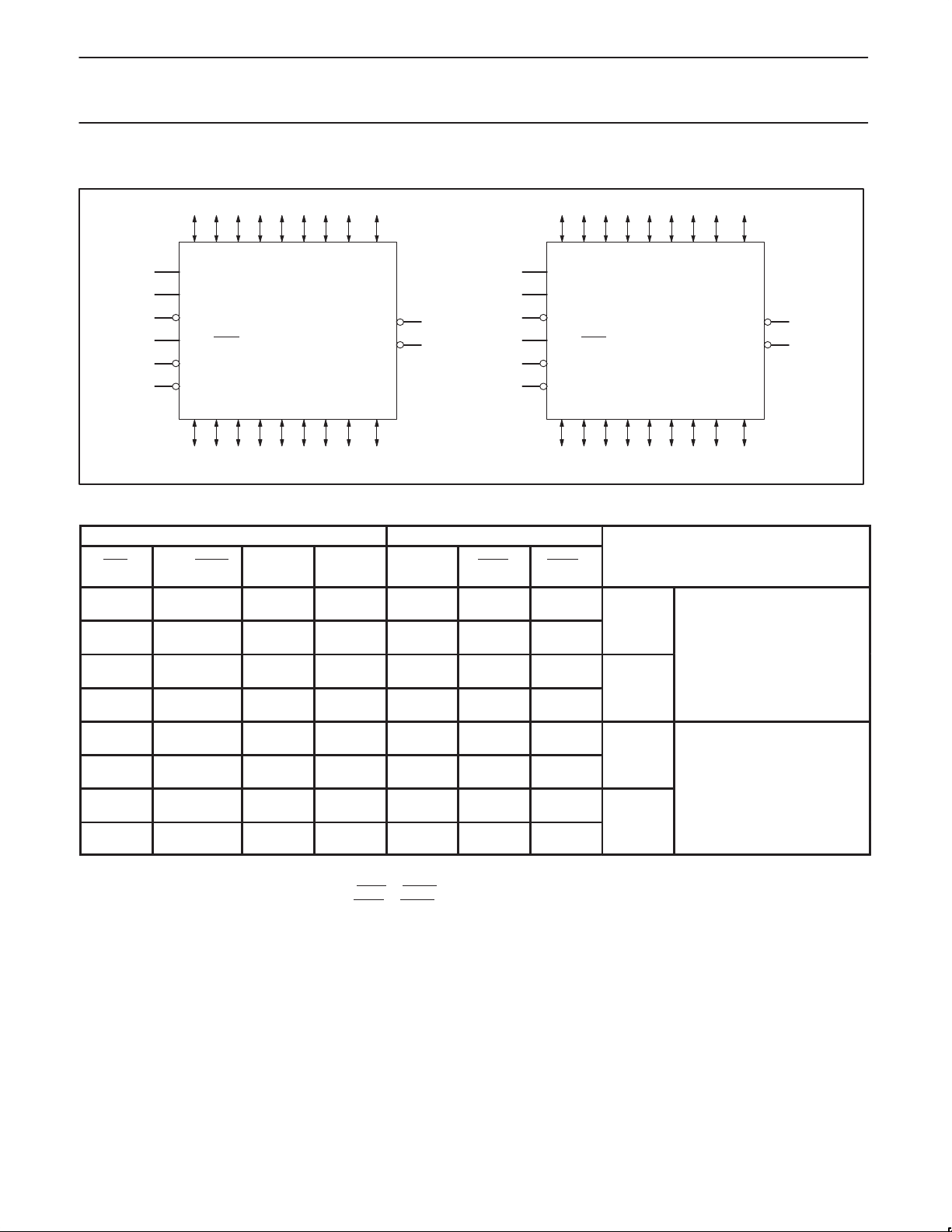
LOGIC SYMBOL
3 5 6 7 8 10 11 12
1A0 1A1 1A2 1A3 1A4 1A5 1A6 1A7
55
28
56
29 OEB
LEA
LEB
SEL
1
ODD/EVEN
OEA
2
1B0 1B1 1B2 1B3 1B4 1B5 1B6 1B7
54 52 51 50 49 47 46 45
PARITY AND ERROR FUNCTION TABLE
INPUTS OUTPUTS
SEL ODD/EVEN
xPAR
(A or B)
H H H
H H L
H L H
H L L
L H H
L H L
L L H
L L L
H = High voltage level
L = Low voltage level
t = Transmit–if the data path is from A→B then ERRt
r = Receive–if the data path is from A→B then ERRr is ERRB
* Blocked if latch is not transparent
Σ of High
Inputs
Even
Odd
Even
Odd
Even
Odd
Even
Odd
Even
Odd
Even
Odd
Even
Odd
Even
Odd
13
1APAR
1ERRA
1ERRB
1BPAR
44
xPAR
(B or A)
H
H
L
L
H
H
L
L
H
L
H
L
L
H
L
H
is ERRA
14
43
ERRt ERRr*
74ABT16899
74ABTH16899
27 25 24 23 22 20 19 18
2A0 2A1 2A2 2A3 2A4 2A5 2A6 2A7
55
28
56
29
LEA
LEB
SEL
1
ODD/EVEN
OEA
2
OEB
2B0 2B1 2B2 2B3 2B4 2B5 2B6 2B7
30 32 33 34 35 37 38 39
PARITY MODES
H
L
L
H
L
H
H
L
H
L
L
H
L
H
H
L
H
L Odd
L
Mode
H
L
H Even
H
Mode
L
H
H Odd
H
Mode
H
H
H Even
H
Mode
H
17
2APAR
2ERRA
2ERRB
2BPAR
40
16
41
SH00083
Feed-through/check parity
Generate parity
1998 Feb 25
4

Philips Semiconductors Product specification
18-bit latched transceiver with 16-bit
parity generator/checker (3-State)
BLOCK DIAGRAM
9–bit
Transparent
Latch
LEA
A0
A1
A2
A3
A4
A5
A6
A7
APAR
LE
Parity
Generator
9–bit
Output
Buffer
1
mux
0
9–bit
Output
Buffer
9–bit
Transparent
Latch
OE
74ABT16899
74ABTH16899
OEB
B0
B1
B2
B3
B4
B5
B6
B7
BPAR
OEA
SEL
ODD/
EVEN
OE
mux
1
0
Parity
Generator
LE
(1 of 2 parity blocks)
FUNCTION TABLE
INPUTS OPERATING MODE
OEB OEA SEL LEA LEB
H H X X X 3-State A bus and B bus (input A & B simultaneously)
H L L L H B → A, transparent B latch, generate parity from B0 - B7, check B bus parity
H L L H H B → A, transparent A & B latch, generate parity from B0 - B7, check A & B bus parity
H L L X L B → A, B bus latched, generate parity from latched B0 - B7 data, check B bus parity
H L H X H B → A, transparent B latch, parity feed-through, check B bus parity
H L H H H B → A, transparent A & B latch, parity feed-through, check A & B bus parity
L H L H X A → B, transparent A latch, generate parity from A0 - A7, check A bus parity
L H L H H A → B, transparent A & B latch, generate parity from A0 - A7, check A & B bus parity
L H L L X A → B, A bus latched, generate parity from latched A0 - A7 data, check A bus parity
L H H H L A → B, transparent A latch, parity feed-through, check A bus parity
L H H H H A → B, transparent A & B latch, parity feed-through, check A & B bus parity
L L X X X Output to A bus and B bus (NOT ALLOWED)
H = High voltage level
L = Low voltage level
X = Don’t care
LEB
ERRA
ERRB
SH00084
1998 Feb 25
5
 Loading...