

Philips 74ABTH16841ADL, 74ABTH16841ADGG, 74ABT16841ADL, 74ABT16841ADGG Datasheet
INTEGRATED CIRCUITS
74ABT16841A
74ABTH16841A
20-bit bus interface latch (3-State)
Product specification
Supersedes data of 1995 Sep 28
IC23 Data Handbook
1998 Feb 27
Philips Semiconductors Product specification
Quiescent supply current
20-bit bus interface latch (3-State)
FEA TURES
•High speed parallel latches
•Live insertion/extraction permitted
•Extra data width for wide address/data paths or buses carrying
parity
•Power-up 3-State
•74ABTH16841A incorporates bus-hold data inputs which
eliminate the need for external pull-up resistors to hold unused
inputs
•Power-up reset
•Ideal where high speed, light loading, or increased fan-in are
required with MOS microprocessors
•Output capability: +64mA/–32mA
•Latch-up protection exceeds 500mA per Jedec Std 17
•ESD protection exceeds 2000V per MIL STD 883 Method 3015
and 200V per Machine Model
QUICK REFERENCE DATA
SYMBOL PARAMETER
C
t
PLH
t
PHL
C
OUT
I
CCZ
I
CCL
IN
Propagation delay
nDx to nQx
Input capacitance VI = 0V or V
Output capacitance VO = 0V or VCC; 3-State 7 pF
pp
74ABT16841A
74ABTH16841A
DESCRIPTION
The 74ABT16841A Bus interface latch is designed to provide extra
data width for wider data/address paths of buses carrying parity.
The 74ABT16841A consists of two sets of ten D-type latches with
3-State outputs. The flip-flops appear transparent to the data when
Latch Enable (nLE) is High. This allows asynchronous operation, as
the output transition follows the data in transition. On the nLE
High-to-Low transition, the data that meets the setup and hold time
is latched.
Data appears on the bus when the Output Enable (nOE
When nOE
Two options are available, 74ABT16841A which does not have the
bus-hold feature and 74ABTH16841A which incorporates the
bus-hold feature.
is High the output is in the High-impedance state.
CONDITIONS
T
= 25°C; GND = 0V
amb
CL = 50pF; VCC = 5V
CC
Outputs disabled; VCC = 5.5V 500 µA
Outputs LOW; VCC = 5.5V 10 mA
) is Low.
TYPICAL UNIT
3.1
2.2
4 pF
ns
ORDERING INFORMATION
PACKAGES TEMPERATURE RANGE OUTSIDE NORTH AMERICA NORTH AMERICA DWG NUMBER
56-Pin Plastic SSOP Type III –40°C to +85°C 74ABT16841A DL BT16841A DL SOT371-1
56-Pin Plastic TSSOP Type II –40°C to +85°C 74ABT16841A DGG BT16841A DGG SOT364-1
56-Pin Plastic SSOP Type III –40°C to +85°C 74ABTH16841A DL BH16841A DL SOT371-1
56-Pin Plastic TSSOP Type II –40°C to +85°C 74ABTH16841A DGG BH16841A DGG SOT364-1
PIN DESCRIPTION
55, 54, 52, 51, 49, 48, 47, 45, 44, 43
42, 41, 40, 38, 37, 36, 34, 33, 31, 30
2, 3, 5, 6, 8, 9, 10, 12, 13, 14
15, 16, 17, 19, 20, 21, 23, 24, 26, 27
4, 11, 18, 25, 32, 39, 46, 53 GND Ground (0V)
1998 Feb 27 853-1797 19025
PIN NUMBER SYMBOL FUNCTION
1D0 – 1D9
2D0 – 2D9
1Q0 – 1Q9
2Q0 – 2Q9
1, 28 1OE, 2OE Output enable inputs (active-Low)
56, 29 1LE, 2LE Latch enable inputs (active rising edge)
7, 22, 35, 50 V
CC
2
Data inputs
Data outputs
Positive supply voltage
Philips Semiconductors Product specification
OPERATING MODE
20-bit bus interface latch (3-State)
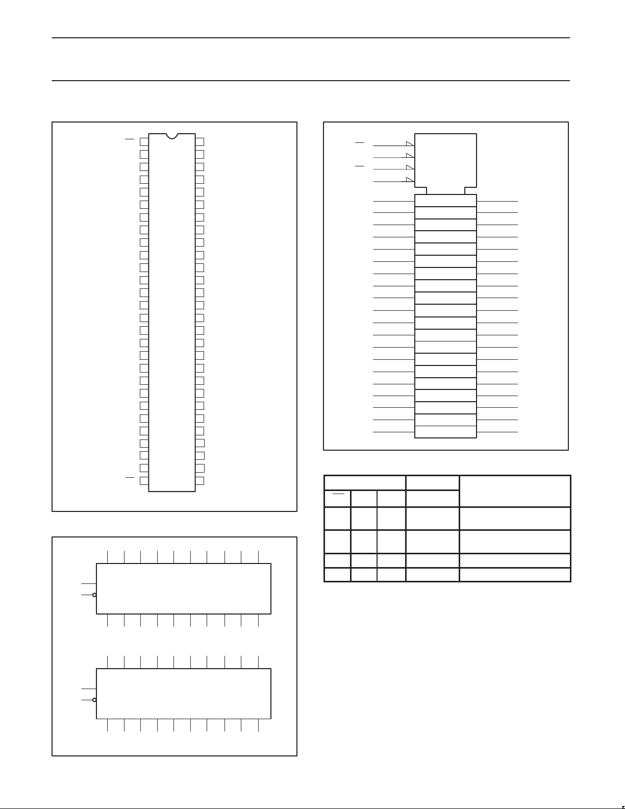
PIN CONFIGURATION
56
55
54
53
52
51
50
49
48
47
46
45
44
43
42
41
40
39
38
37
36
35
34
33
32
31
30
29
SA00076
1LE
1D0
1D1
GND
1D2
1D3
V
CC
1D4
1D5
1D6
GND
1D7
1D8
1D9
2D0
2D1
2D2
GND
2D3
2D4
2D5
V
CC
2D6
2D7
GND
2D8
2D9
2LE
1D8 1D9
1Q8 1Q9
2D8 2D9
2Q8 2Q9
1OE
GND
V
GND
GND
V
GND
2OE
LOGIC SYMBOL
55 54 52 51 49 48 47 45 44 43
1D0 1D1 1D2 1D3 1D4 1D5 1D6 1D7
56
1LE
1
1OE
1Q0 1Q1 1Q2 1Q3 1Q4 1Q5 1Q6 1Q7
2 3 5 6 8 9 10 12 13 14
42 41 40 38 37 36 34 33 31 30
2D0 2D1 2D2 2D3 2D4 2D5 2D6 2D7
29
2LE
28
2OE
2Q0 2Q1 2Q2 2Q3 2Q4 2Q5 2Q6 2Q7
1Q0
1Q1
1Q2
1Q3
CC
1Q4
1Q5
1Q6
1Q7
1Q8
1Q9
2Q0
2Q1
2Q2
2Q3
2Q4
2Q5
CC
2Q6
2Q7
2Q8
2Q9
1
2
3
4
5
6
7
8
9
10
11
12
13
14
15
16
17
18
19
20
21
22
23
24
25
26
27
28
74ABT16841A
74ABTH16841A
LOGIC SYMBOL (IEEE/IEC)
1
1OE
56
1LE
28
2OE
29
2LE
55
1D0
54
1D1
52
1D2
51
1D3
49
1D4
48
1D5
47
1D6
45
1D7
44
1D8
43
1D9
42
2D0
41
2D1
40
2D2
38
2D3
37
2D4
36
2D5
34
2D6
33
2D7
31
2D8
30
2D9
FUNCTION TABLE
INPUTS OUTPUTS
nOE nLE nDx nQ0 – nQ9
L
H
L
L
L
H X X Z High impedance
L L X NC Hold
H = High voltage level
h = High voltage level one set-up time prior to the High-to-Low LE
transition
L = Low voltage level
l = Low voltage level one set-up time prior to the High-to-Low LE
transition
↓ = High-to-Low LE transition
NC= No change
X = Don’t care
Z = High impedance “off” state
L
H
H
↓
l
↓
h
1D
3D
EN2
C1
EN4
C3
2 ∇
4 ∇
L
H
L
H
2
1Q0
3
1Q1
5
1Q2
6
1Q3
8
1Q4
9
1Q5
10
1Q6
12
1Q7
13
1Q8
14
1Q9
15
2Q0
16
2Q1
17
2Q2
19
2Q3
20
2Q4
21
2Q5
23
2Q6
24
2Q7
26
2Q8
27
2Q9
SH00081
Transparent
Latched
1998 Feb 27
15 16 17 19 20 21 23 24 26 27
SH00023
3
 Loading...