

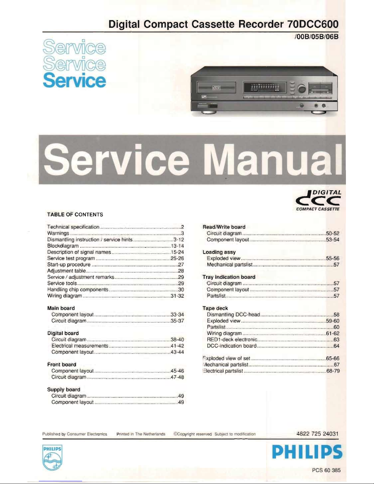
Philips 70DCC600, 70DCC600/008, 70DCC600/058, 70DCC600/068 Service Manual
~@NOO
~@NOO
Service
Digital Compact Cassette Recorder 70DCC600
1008/058/068
CCC
COMPACT CASSETTE
TABLE
OF CONTENTS
Technical specification 2
W~~
~
Dismantling instruction I service hints 3-12
Blockdiagram 13-14
Description of signal names 15-24
Service test program 25-26
Start-up procedure 27
Adjustment table 28
Service
I adjustment remarks 29
Service tools 29
Handling chip components 30
Wiring diagram 31-32
Main
board
Component layout 33-34
Circuit diagram 35-37
Digital
board
Circuit diagram 38-40
Electrical measurements .41-42
Component layout .43-44
Front
board
Component layout .45-46
Circuit diagram .47-48
Supply
board
Circuit diagram .49
Component layout .49
ReadlWrite
board
Circuit diagram 50-52
Component layout 53-54
Loading
assy
Exploded view 55-56
Mechanical partslist 57
Tray
indication
board
Circuit diagram 57
Component layout 57
Partslist. 57
Tape
deck
Dismantling DCC-head 58
Exploded view 59-60
Partslist. 60
Wiring diagram 61-62
RED1-deck electronic 63
DCC-indication board 64
Exploded view of set 65-66
\,1echanical parts list 67
:::Iectrical partslist 68-79
PublishedbyConsumer Electronics PrintedinThe Netherlands ©Copyright reserved Subjecttomodification
4822 725
24031
PHILIPS
PCS 60 385
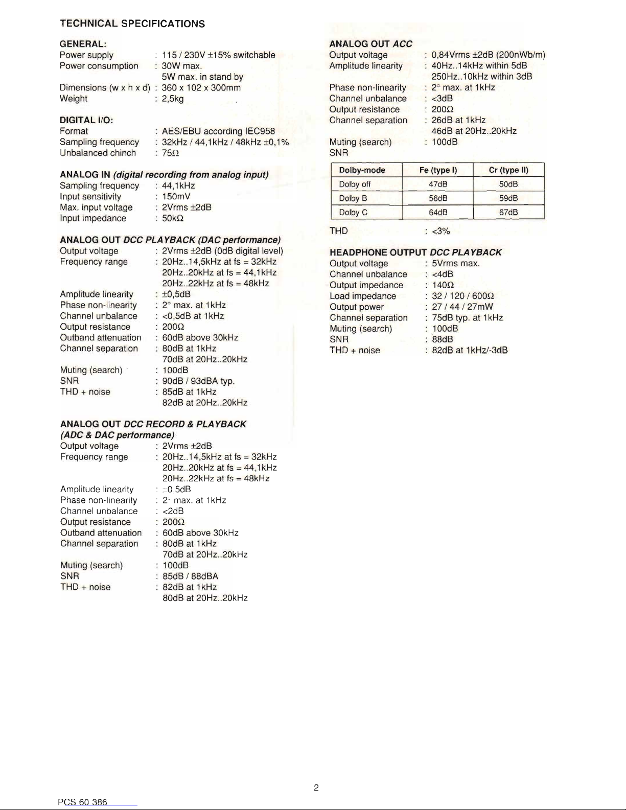
TECHNICAL
SPECIFICATIONS
GENERAL:
Power supply
Power consumption
Dimensions
(w
x h x
d)
Weight
DIGITAL 1/0:
Format
Sampling frequency
Unbalanced chinch
115
I 230V +15% switchable
30W max.
5W
max.instand by
: 360 x 102 x 300mm
: 2,5kg
: AES/EBU according IEC958
: 32kHz
144,1 kHz 148kHz
+0,1
%
: 75Q
ANALOG OUT
ACC
Output voltage
Amplitude linearity
Phase non-linearity
Channel unbalance
Output resistance
Channel separation
Muting (search)
SNR
: 0,84Vrms ±2dB
(200nWb/m)
: 40Hz..14kHz within 5dB
250Hz
..1OkHz
within 3dB
:
2°
max.at1
kHz
: <3dB
: 200Q
: 26dB at 1kHz
46dB at 20Hz
..
20kHz
: 100dB
ANALOG
IN
(digital
recording
from
analog
input)
Sampling frequency :
44,1
kHz
Input sensitivity . 150mV
Max. input voltage 2Vrms +2dB
Input impedance 50kQ
Dolby-mode
Fe
(type
I)
Cr
(type
II)
Dolby
off
47dB
50dB
Dolby
B
56dB
59dB
Dolby
C
64dB 67dB
ANALOG OUT DCC
PLA
YBACK
(DAC
performance)
THO
: <3%
HEADPHONE OUTPUT
DCC PLA YBACK
Output voltage
Frequency range
Amplitude linearity
Phase non-linearity
Channel unbalance
Output resistance
Outband attenuation
Channel separation
Muting (search) .
SNR
THO
+ noise
: 2Vrms +2dB
(OdB
digital level)
: 20Hz
..
14,5kHzatfs
= 32kHz
20Hz
..
20kHz at
fs=44,1
kHz
20Hz
..
22kHzatfs
= 48kHz
: +0,5dB
: 2°
max.at1
kHz
<0,5dBat1kHz
: 200Q
: 60dB above 30kHz
: 80dB
at
1kHz
70dB
at
20Hz..20kHz
100dB
90dB
I 93dBA
typo
85dBat1kHz
82dB
at
20Hz..20kHz
Output voltage
Channel unbalance
Output impedance
Load impedance
Output power
Channel separation
Muting (search)
SNR
THO
+ noise
: 5Vrms max.
: <4dB
: 140Q
:
32
I 120 I 600Q
:
27
I 44 I 27mW
: 75dB
typoat1kHz
: 100dB
: 88dB
: 82dB
at
1kHzI·3dB
ANALOG OUT
DCC
RECORD & PLAYBACK
(ADC &
DAC
performance)
Output voltage
Frequency range
Amplitude linearity
Phase non-linearity
Channel unbalance
Output resistance
Outband attenuation
Channel separation
Muting (search)
SNR
THO + noise
PCS
60 386
: 2Vrms +2dB
: 20Hz
..
14,5kHzatfs
= 32kHz
20Hz
..
20kHzatfs=44,1
kHz
20Hz
..
22kHzatfs
= 48kHz
: +0,5dB
: 2° max.
at1kHz
: <2dB
: 200Q
: 60dB above 30kHz
: 80dB
at1kHz
70dBat20Hz..20kHz
: 100dB
: 85dB
I 88dBA
: 82dB
at
1kHz
80dB
at
20Hz..20kHz
2
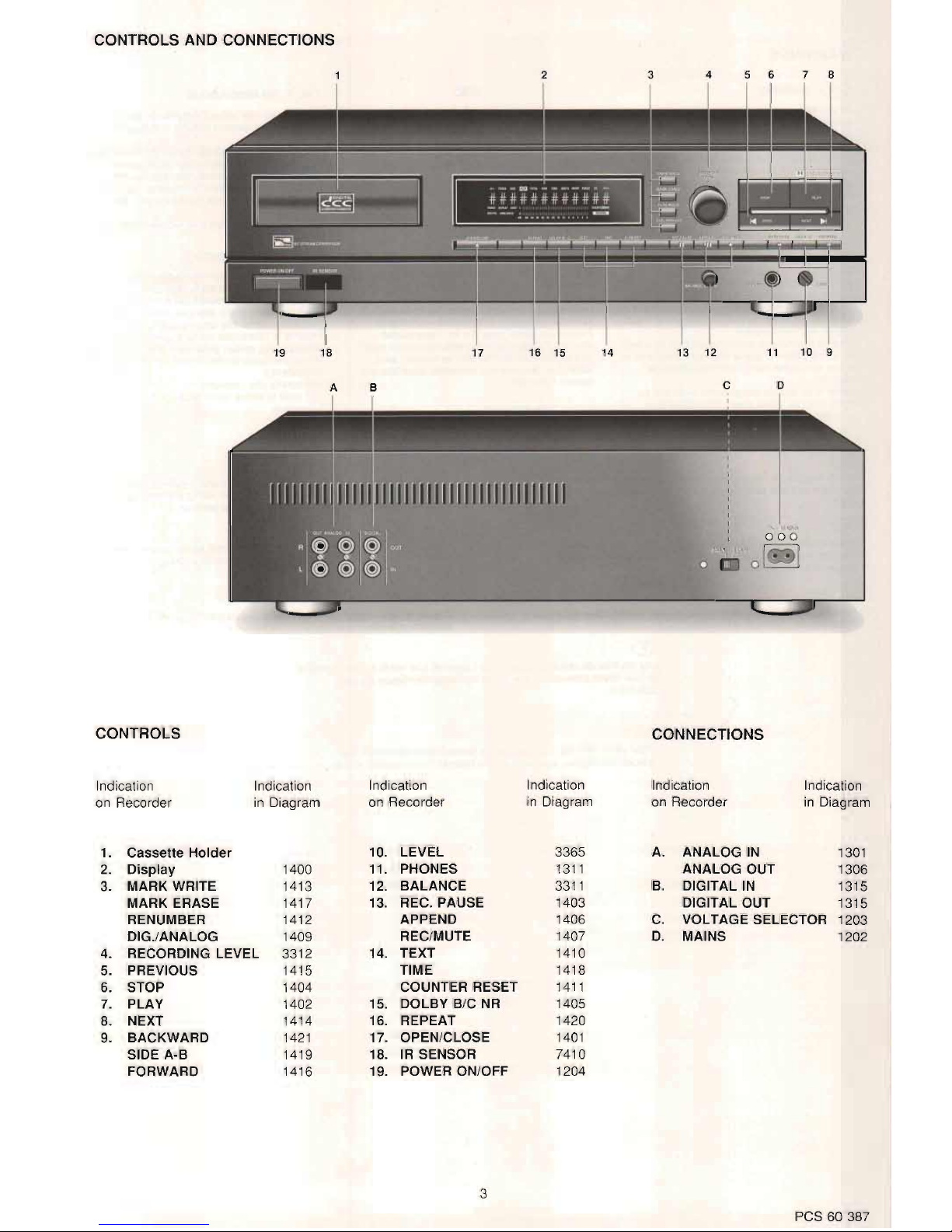
CONTROLS AND CONNECTIONS
2
3
4 5 6 7 8
19
18
A B
17
16 15
14
13
12
c
11
10 9
o
"",
1-1\1>1;\
000
'org
CONTROLS
CONNECTIONS
Indication Indication
Indication
Indication
Indication
Indication
on
Recorder
in
Diagram
on
Recorder
in
Diagram
on
Recorder
in
Diagram
1. Cassette
Holder
10. LEVEL 3365 A. ANALOG
IN
1301
2.
Display 1400
11.
PHONES 1311
ANALOG
OUT
1306
3. MARK WRITE 1413
12.
BALANCE 3311 B.
DIGITAL
IN
1315
MARK ERASE 1417
13.
REC.PAUSE
1403 DIGITAL OUT
1315
RENUMBER 1412
APPEND 1406
C.
VOLTAGE SELECTOR
1203
DIG.lANALOG 1409
REC/MUTE 1407
D.
MAINS
1202
4.
RECORDING LEVEL
3312
14.
TEXT 1410
5.
PREVIOUS 1415
TIME 1418
6. STOP
1404
COUNTER RESET 1411
7.
PLAY
1402
15.
DOLBY B/C NR 1405
8.
NEXT
1414
16. REPEAT 1420
9.
BACKWARD 1421 17.
OPEN/CLOSE 1401
SIDE A-B
1419
18. IR SENSOR 7410
FORWARD 1416
19.
POWER ON/OFF
1204
3
pes
60
387
WARNINGS
® WARNING
All
les
and
many
other
semi-conductors are
susceptible to electrostatic discharges (ESD).
Careless
handling
during
repair
can
reduce
life
drastically.
When
repairing. make
sure
that
you
are
connected
with
the
same potentialasthe mass
of
the
set
via
a wrist wrap with resistance.
Keep components and tools also at this
potential.
CD
ATTENTION
Taus les IC
et
beaucoup
d'autres
semi-conducteurs
sont
sensibles
aux
dacharges statiques (ESD).
Leur
longevite
pourrait etre considerablement
ecourtee par
Ie
fait
qu'aucune precaution n'est
prise
aleur manipulation.
Lors
de
reparations. g'assurer
de
bien
atre falie
au
meme
potential
quelamasse de I'appareil at
anfiler
Ie
bracelet
sarti
d'une resistance de
securite.
Veilleraco
que
les composants
ainsi
que les
cUlils
que
I'on
utilise
soient egalement ace
potentiel.
ESD
® WARNUNG
Aile ICs und viele andere Halbleiter sind
emplindlich gegen elektrostatische Entladungen
(ESD).
Unsorgtiiltige
Behandlung bei
der
Reparatur
kann die Lebensdauer drastisch vermindern.
Sorgen sie datur,
dass
Sie im Reparaturfall
l.iber
ein
Pulsarmband
mit
Widerstand
mit
dem
Massepotential des Gerates verbunden
sind.
halten Sie Bauteile und Hillsminel ebenlalls auf
diesem Potential.
@ WAARSCHUWING
Aile IC's en vele andere haltgeleiders zijn
gevoelig voor electrostatische ontladingen
(ESD).
Onzorgvuldig behandelen tijdens reparatie kan
de levensduur drastisch doen verminderen.
Zorg erYoor dat u tijdens reparatie
via
een
polsband
met
weerstand verbonden bent
met
hetzeltde potentiaal als de
massa
van het
apparaal.
Houd
componenten
en hulpmiddelen
oak
op
ditzeltde potentiaal.
CJ) AVVERTIMENTO
TuttiIee parecchi semi-conduttori sono
sensibili aile scariche statiche (ESD).
La
loro longevita potrebbe essere fortemente
ridatta
in
casodinon
osservazione della piu
grande cauzione alia loro manipolazione.
Durante
Ie
riparazioni occorre quindi essere
collegato alia
stesso
potenziale che quello della
massa dell'apparecchio tramiteunbraceialetta
a resistenza.
Assicurarsi
che
i componenti e anche
gli
utensili
con
qualisilavara siano anche a questa
potenziale.
@
Safety regulations require that the set be restoredtoits original
condition
and
that parts
which
are identical
with
those specified
be
used.
®
Veiligheidsbepalingen vereisen, dat het apparaatinzijn
oorspronkelijke
toestand
wordt
teruggebracht en
dat
onderdelen, identiek aan de
gespeciliceerde worden toegepasl.
@Varo!
Avattaessajasuojalukitus ohitettaessa olet alttiina nakymattomalle
lasersiiteilylle. Alii katso sateeseen.
CD
Bei
jeder Reparatur
sind
die
geltenden Sicherheitsvorschriften
zu
beachten. Der Originalzustand des Gerats dart
nicht
verandert werden
fUr
Reparaturen
sind
Original-Ersatzteilezuverwenden.
CD
Le
normedisicurezza esigona
che
I'apparecchio venga rimesso nelle
condizioni originali e
che
siano utilizzati pezzidirtcambiago identici a
quelli
specificati.
® Varning!
Osynlig laserstnllning
niir
denna del
iir
oppnad
och sparren
iir
urkopplad.
Betrakta ej stnllen.
CD
Les
normesdesecurite exigent que I'appareil
soit
remis a "etat d'arigine
et
que soient utili
sees
les pieces de rechange identiques a celles
specifiees.
-Pour votre securite, ces documents doivent etre utilises par des
specialistes agrees, seuls habilites a reparer votre appareil
en
panne-.
4
pes
60 388
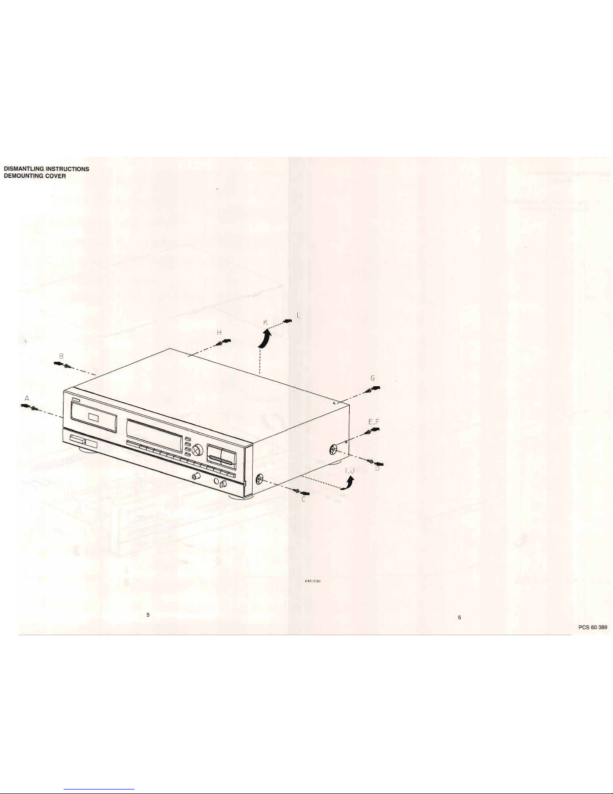
DISMANTLING INSTRUCTIONS
DEMOUNTING COVER
B
~-
A
~----
5
L
HAS.109Q
G
~
E,F
~
5
pes
60 389
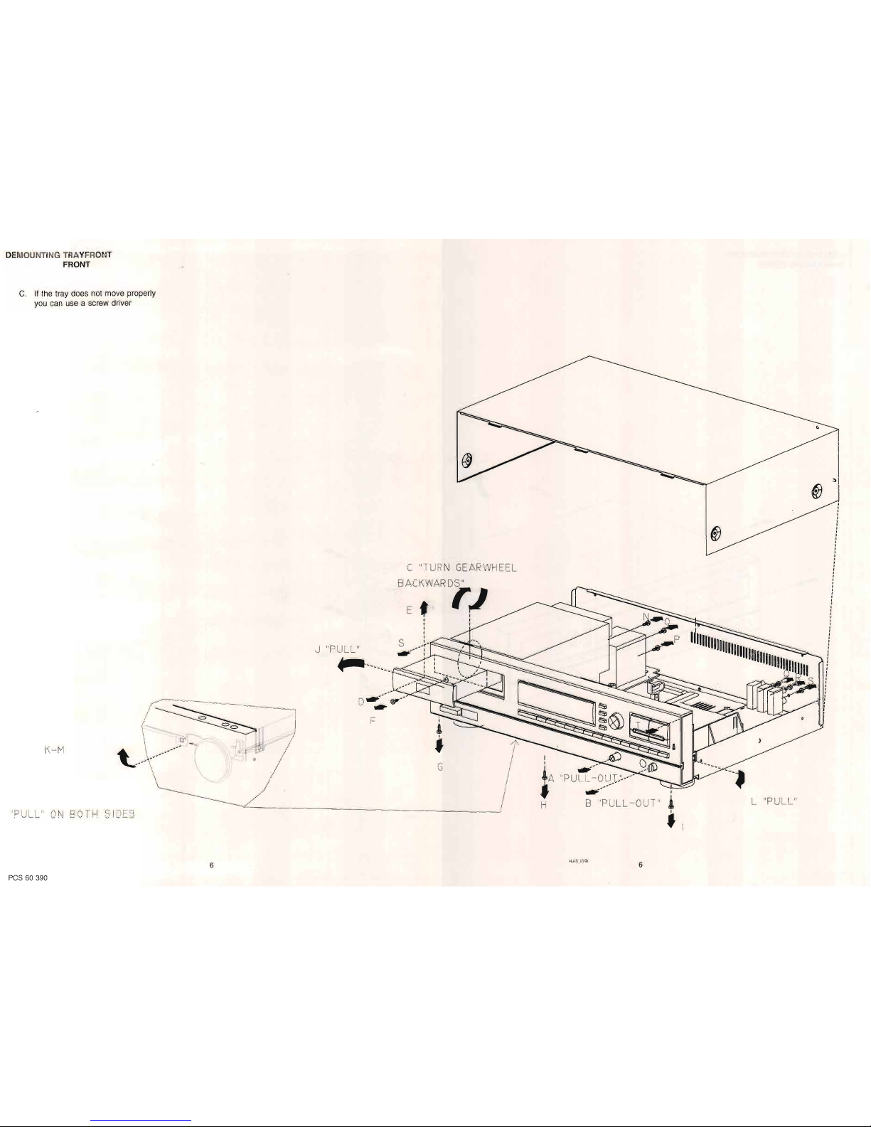
DEMOUNTING TRAYFRONT
FRONT
C.Ifthe tray does not move properly
you can use a screw driver
K-M
'PULL"ONBOTH SIDES
pes
60 390
6
J "PULL"
~-------
F
C "TURN GEARWHEEL
BACKWARDS"
Et
rJ
G
HAS.I091
6
L "PULL"
I
I
I
,
,
I
,
I
,
I
I
I
I
,
I
I
I
I
,
I
,
I
I
,
I
,
,
,
,
,
,
•
,
I
I
I
,
I
I
I
,
I
,
I
,
I
I
,
I
,
,
,
,
I
,
I
,
I
I
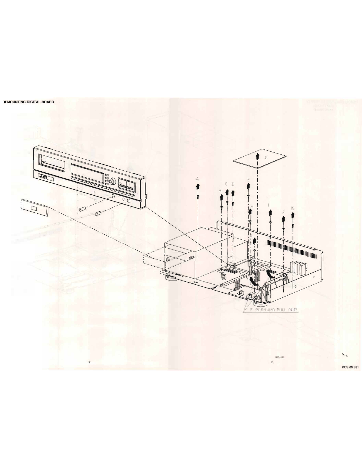
DEMOUNTING DIGITAL BOARD
7
A
f
t
!
l
!
!
i
C D
B.ff
! , .
Ti r
I i I
: I
:
K
• t f
t i ,
T I
I
I
OUT"
F "PUSH
AND
PULL
HAS.I09?
8
pes
60
391
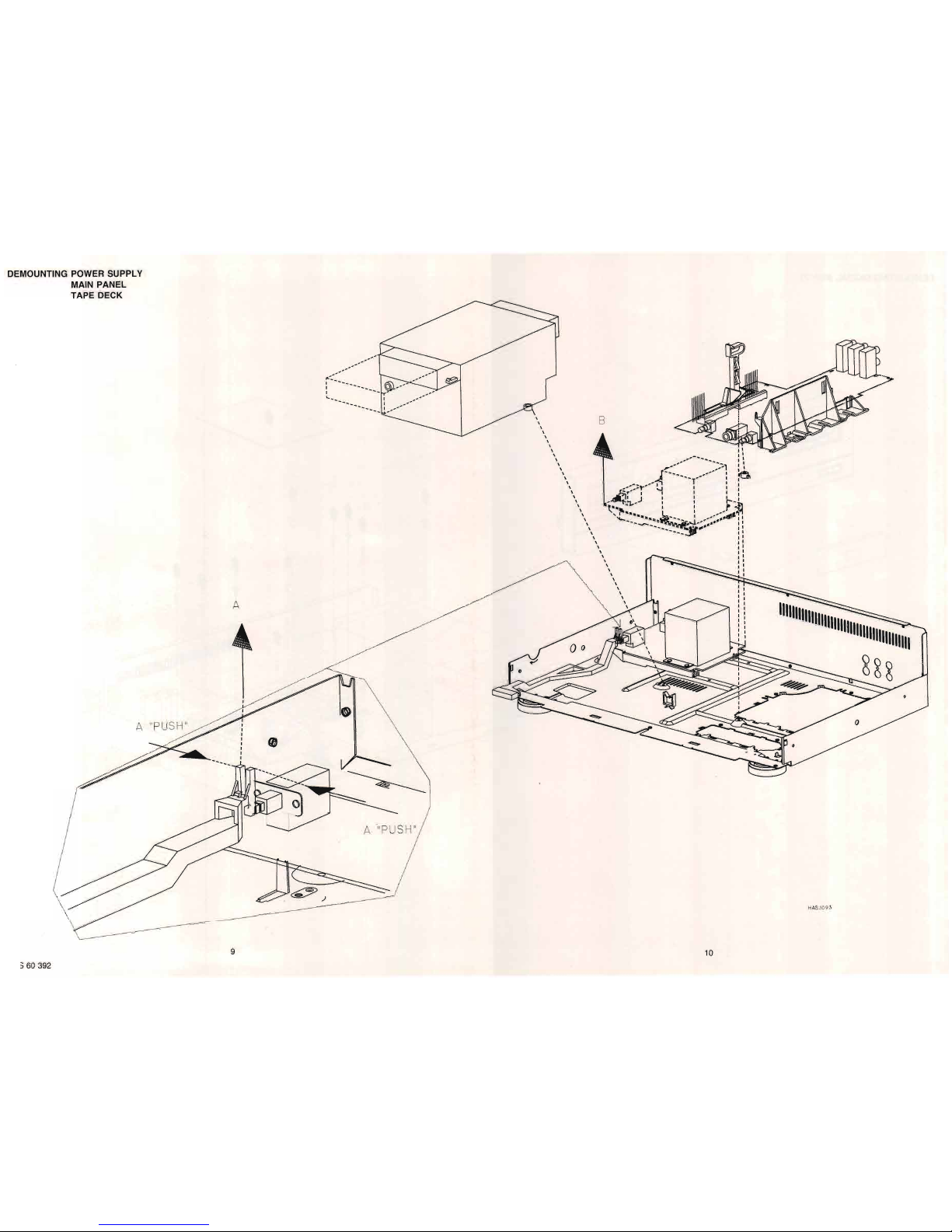
DEMOUNTING POWER SUPPLY
MAIN PANEL
TAPE DECK
HAS.I093
11111111111111111111111111111111111111111
888
"
"
;"..--
.....__I '
",;
..
:-:.,
I
~
1---- ----- :
~
_~_
/~
T
':
--
_--,..
-..J
' "
~
"
I'
I
I,
'J'
, ,
-
-'1--
, ,
r---~'
~
..
, ' :
-'
,1
....'
_-
.,.-
'4... -
__~~...
_ I
;,'
....
·~II
.....__...
- .......
...j.." _
...
,.-
I I
"'--..
-1:1"-
I I
-
...
__
~
It
"
"
"
"
"
I'
,'
I:
B
\
\
\
\
\
\
\
\
\
\
\
\
\
\
\
\
\
\
\
\
\
\
\
\
\
\
\
\
\
\
\
\
\
\
\
\
\
\
\
\
\
\
---
--
--
--
---
--
...
_-
: ------
..
I
'-.
-.
'-.
".
A
9
10
pes
60 392
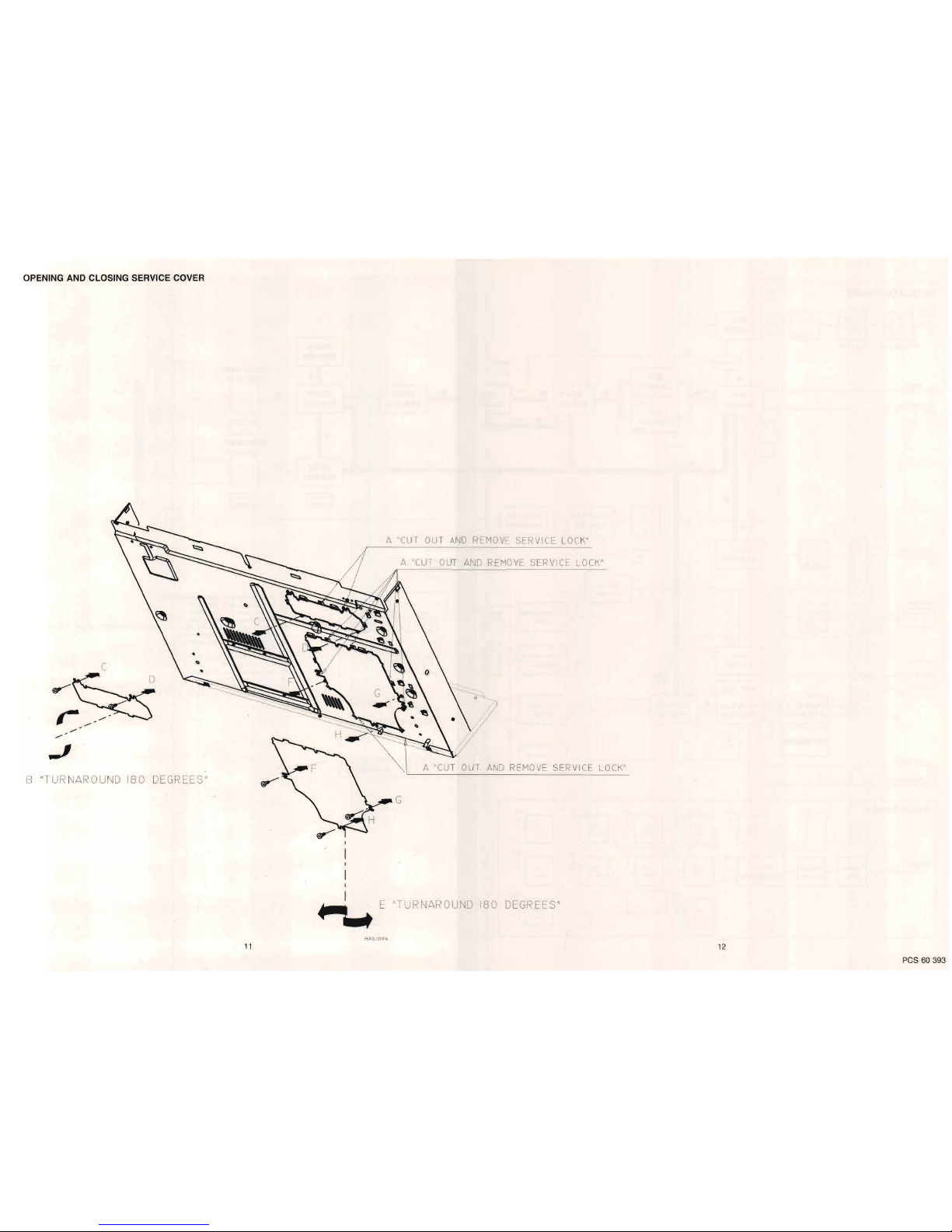
OPENING AND CLOSING SERVICE COVER
G
A "CUT
OUT
AND
REMOVE
SERVICE LOCK"
A
"CUT
OUT
AND
REMOVE
SERVICE LOCK"
)
A "CUT
OUT
AND
REMOVE
SERVICE LOCK"
c
B "TURNAROUND 180 DEGREES"
"TURNAROUND 180 DEGREES"
HAS
1094
11
12
pes
60
393
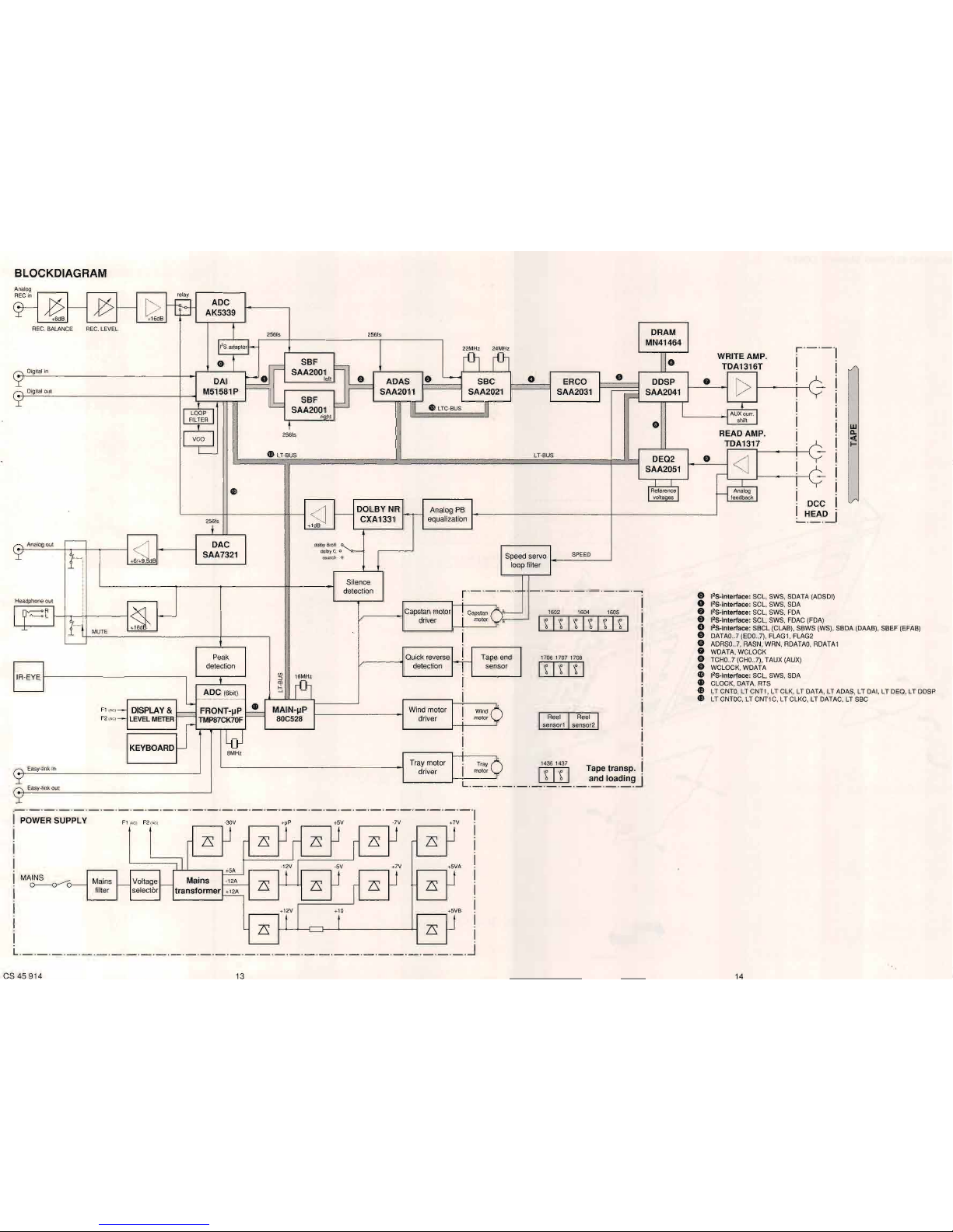
BLOCKDIAGRAM
w
a.
~
ATA1
SOl)
)
WS), SBDA (DAAB), SBEF (EFAB)
C
D
A,
LT ADAS, LT DAI, LT DEQ, LT DDSP
DATAC,LTSBC
A log
n.
REC
in
relay
7-
p
-
p
-
[>
S
ADC
AK5339
+6dB
+16dB
REC.BALANCE
REC.
LEVEL
T
DRAM
256'5
256ls
IlS
adaPtor~
MN41464
fDl
fDl
r'-'
G f
10
WRITE AMP.
1
dJF
SBF
TDA1316T
Digital
in
SAA2001 h
•
1
DAI
left e
ADAS
e
'--
SBC
•
ERCO
DDSP
•
[>
Digital out
M51581P
IlL
SBF r
SAA2011 SAA2021
SAA2031
;::;::
SAA2041
!
Gl
LTC·BUS
N
I
I
1
SAA2001
I AUXcurr.
Ir
LOOP
~nht
FILTER
0
I
shift
1
t t
Ir
25615
READ AMP.
1
vco
TDA1317
i
l-
lfJ
LT·BUS
LT·BUS
DEQ2
0
<J
!
L
SAA2051
~
1
1
~
I
Reference
I H
Analog
1
vol1aoes
feedback
DC
<J
f---
DOLBY NR
f---
Analog
PB
1
HEA
2sts
CXA1331
equalization
~.-
+1dB
~
Analog out
-
+~B
DAC
dolbyBloll
o~
'i'
A.
SAA7321
dolby
c 0
Speed
servo
SPEED
I--
search
0
loop
filter
Silence
detection
r'-'-'-'-
'-'-'-'-'-'-'-'-'
G
I'S-interlace:
SCL, SWS, SDATA (AD
Headphone
out
I
•
"S-interlace:
SCL, SWS, SDA
~~RI
S}
Capstan
motor
I
J:.
1602
1604
e
"S-interlace:
SCL, SWS,
FDA
I--
.
CaPSta~
(
r--
1605
1
"---<>
L I
A.
driver
i
motor
yB
u::IIIIIillIIl
e
"S-interlace:
SCL, SWS, FDAC (FDA
-= l-l
I
0
"S-interlace:
SBCL (CLAB), SBWS (
MUTE
1
•
DATAO..7
(EDO..7), FLAGt, FLAG2
L--
1
•
ADRSO..7,
RASN, WRN,
RDATAO,
RD
Quick
reverse
If-
•
WDATA, WCLOCK
Peak
Tape
end
1706
1707
1708
1
0
TCHO..7
(CHO..7), TAUX
(AU
X)
detection detection
sensor
[illJIJ
0 WCLOCK, WDATA
IR-EYE
fDl
1
~
"S-interlace:
SCL, SWS, SDA
•
I
Gl
CLOCK, DATA,
RTS
ADC (6bit)
1
lfJ
LT
CNTO,LTCNT1, LT CLK,LTOAT
I
Gl
LT
CNTOC,
LT CNTtC,LT CLKC, LT
L.
1---------
F1
IAC)-
DISPLAY &
f---
FRONT-IJP I
Gl
MAIN-IJP
Wind
motor
1
Wj~¢
1
;,~-
""'-
.....
~
TMP87CK70F
80C528
driver
;
motor
_
rReel 1Reel
1
~
sensor1
sensor2
loJ
I
1
KEYBOARD
1
8M
Hz
i
!
;0
.
Tray
motor
Tray 1436 1437
Easy-link
in
driver
I
motor _ [Iill Tape
tran~p.
!
and loadingJ
Easy-link
out
L.
'-'-'-'-'-'-'-'-'-'
VB
VA
lAC)
(ACj
0
J
i
J I
J
ZSJ
ZS
ZS
ZS ZS
I
11
E J I
ZS
,:r
0
~
>-
Mains
I--
Voltage
I--
Mains
·12A
ZS
ZS
filter
selector
transformer
~
+f
I
T
zsO
ZS
MA~
_._._._._._._._._._.-.-._._._._._._._._._._._._._._._.-'-'-'-'1
POWER SUPPLY
F1
F2
30V
+~P
sv
7V
+7V·
L._._._._._._._._._._._._._._._._._._._._._._._._._._._._._._.J
CS 45 914
13
14
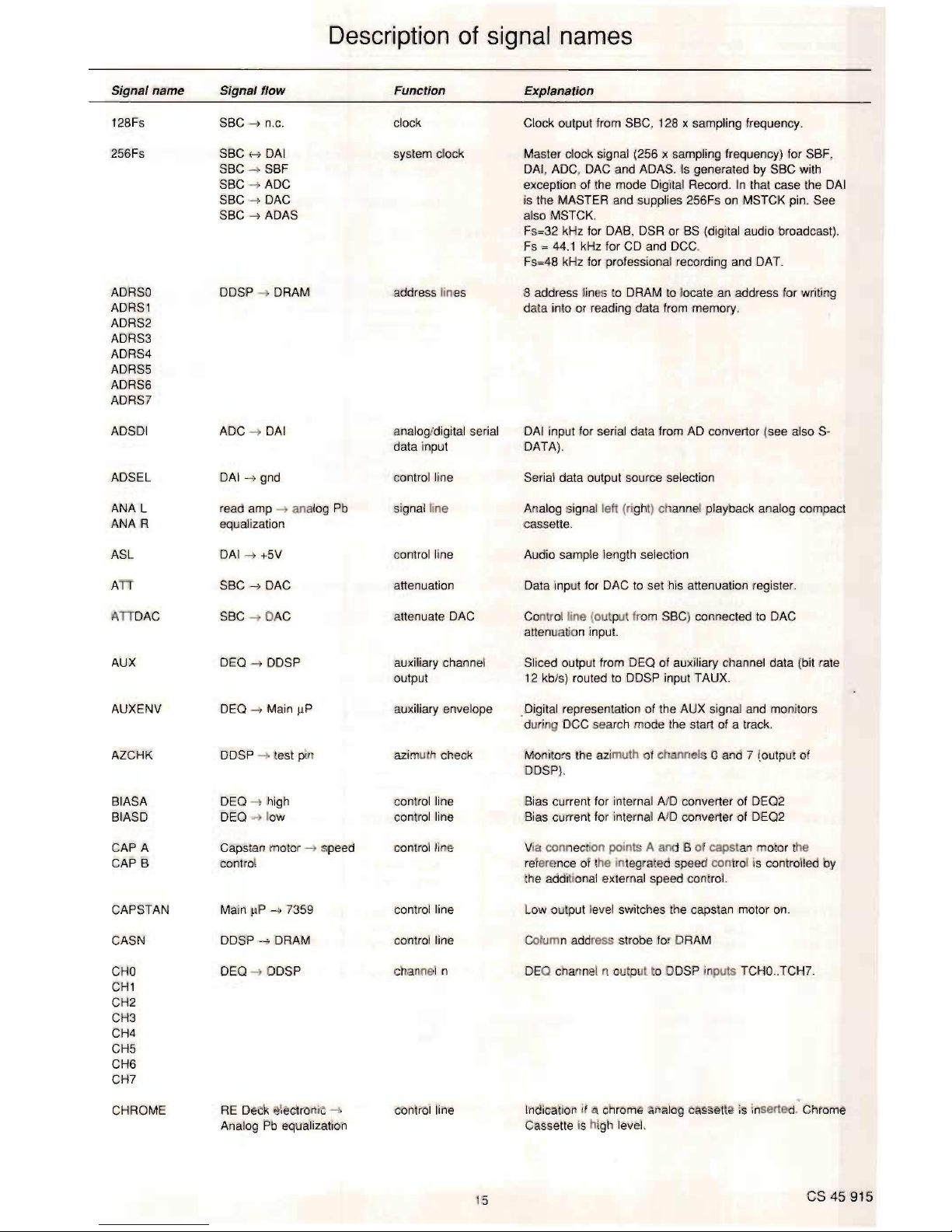
Description
of
signal
names
Signal name Signal flow Function
128Fs SBC
-->
n.C.
clock
256Fs SBC
.....
DAI system clock
SBC
-->
SBF
SBC
-->
ADC
SBC
-->
DAC
SBC
-->
ADAS
Explanation
Clock output from SBC, 128 x sampling frequency.
Master clock signal (256 x sampling frequency) for SBF,
DAI, ADC, DAC and ADAS.
Is
generated by SBC with
exception of the mode Digital Record.
In
that case the
DAI
is the MASTER and supplies 256Fs on MSTCK pin. See
also MSTCK.
Fs=32 kHz for DAB, DSR or
BS
(digital audio broadcast).
Fs=44.1
kHz forCDand DCC.
Fs=48 kHz for professional recording and OAT.
ADRSO
ADRS1
ADRS2
ADRS3
ADRS4
ADRS5
ADRS6
ADRS7
ADSDI
ADSEL
ANA L
ANA R
ASL
An
AnDAC
AUX
AUXENV
AZCHK
BIASA
BIASD
CAP A
CAP B
CAPSTAN
CASN
CHO
CH1
CH2
CH3
CH4
CH5
CH6
CH7
CHROME
DDSP
-->
DRAM
ADC
-->
DAI
DAI
-->
gnd
read amp
-->
analog Pb
equalization
DAI
-->
+5V
SBC
-->
DAC
SBC
-->
DAC
DEQ
-->
DDSP
DEQ
-->
Main IlP
DDSP
-->
test pin
DEQ
-->
high
DEQ
-->
low
Capstan motor
-->
speed
control
Main IlP
-->
7359
DDSP
-->
DRAM
DEQ
-->
DDSP
RE
Deck electronic
-->
AnalogPbequalization
address lines
analog/digital serial
data input
control line
signal line
control line
attenuation
attenuate DAC
auxiliary channel
output
auxiliary envelope
azimuth check
control line
control line
control line
control line
control line
channel n
control line
15
8 address lines
to
DRAM to locateanaddress for writing
data into or reading data from memory.
DAI input for serial data from AD convertor (see also S-
DATA).
Serial data output source selection
Analog signal left (right) channel playback analog compact
cassette.
Audio sample length selection
Data input for DAC to set his attenuation register.
Control line (output from SBG) connected to DAC
attenuation input.
Sliced output from DEQ of auxiliary channel data (bit rate
12 kb/s) routed to DDSP input TAUX.
_Digital representation of the AUX signal and monitors
during DCC search mode the start of a track.
Monitors the azimuth of channels 0 and 7 (output of
DDSP).
Bias current for internal AID converter of DEQ2
Bias current for internal AID converter of DEQ2
Via connection points A and B of capstan motor the
reference of the integrated speed control is controlled by
the additional external speed control.
Low output level switches the capstan motor on.
Column address strobe for DRAM
DEQ channel n output
to
DDSP inputs
TCHO
..TCH7.
Indication if a chrome analog cassette
is
inserted. Chrome
Cassette is high level.
CS45915
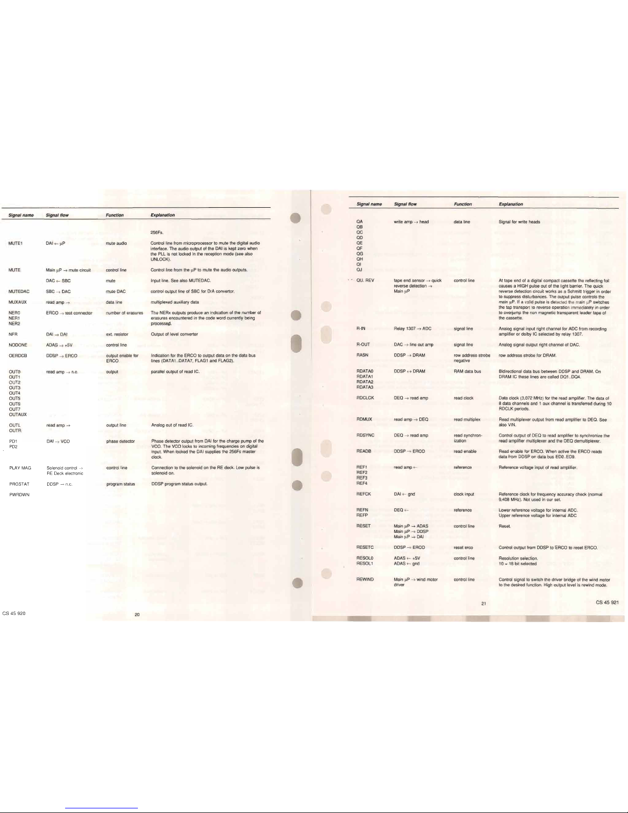
Signal name Signal flow Function Explanation
Signal name
Signal flow
Function
Explanation
EFAB ERCO
-->
SBC Error flag
1
2
S error flag directly connectedtoSBC input SBEFtogive
CKACO
DAI
-->
n.C.
Testpin
Frequency accuracy check output.
(1
=frequency deviation
the error status of bytes being transferred during data
> 0,14% = error condition)
playback (see also SBEF).
F24 DDSP
<- SBC 24.576 MHz master
Master clock from SBC
to
DDSP and DEQtodetermine
CLAB
ERCO H SBC
1
2
S bit clock
Bit clock I/O from ERCO directly connected to SBC I/O
DEQ
<- SBC clock the length of tape frame and inter frame gap.
In
case of a
SBCL pin (see also SBCL).
digital recording this clock
is
not synchron with the
sampling frequency and its related frequencies, coming
CLOCK Main
~P
-->
Front
~P
clock
Clock frequency for data transfer.
from the
DAI
(see also CLK24).
CLK22
SBC
-->
n.C.
22.5792 MHz clock
FAST
Main
~P
-->
wind motor
control line High output level switches +12V supply
to
the motor bridge
output
driver
in
ordertoobtain high speed.
CLK24
SBC
-->
DDSP
24.576 MHz master
Master clock from SBC to DDSP, ADAS and DEQ to
FDA SBF
H ADAS filtered data Bidirectional serial data line between SBF and ADAS
SBC
-->
DEQ
clock
determine the length of tape frame and inter frame gap.
In
SBC H ADAS respectively SBC and ADAS.
SBC
-->
ADAS
case of a digital recording this clock
is
not synchronous
with the sampling frequency and its related frequencies,
Data transfer
in
12S format, carrying32sub-band channels
coming from the DAI (see also F24).
digital audio data (see also FDAF and FDAC). Each SWS
period 2x18 bits data are transferred.
DAAB
ERCO
H SBC
serial data
(12S)
Bidirectional 12S serial data line between ERCO and SBC
(see also SBDA).
FDAC
ADAS
H SBC filtered data Filtered data transfer between ADAS and SBC (see also
FDA).
DATA
Front
~P
H Main
~P
data line
Communication line Front
~P
- Main
~P.
FDAF ADAS H SBF filtered data Filtered data transfer between ADAS and SBF (see also
DATAO
ERCO H DDSP
data line n
Parallel data lines for symbol transfer between ERCO and
FDA).
DATA1
DDSP. DDSP
is
the master.
DATA2
See also
EDO..ED7.
FDIR
SBC
-->
SBF direction control Control line output from SBC to SBF and ADAStoindicate
DATA3
SBC
-->
ADAS the mode of operation. FDIR=1; decoding mode (sub-band
DATA4
synthesis)
DATA5
FDIR=O;
encoding mode (sub-band analysis).
DATA6
DATA7
FLAG1
ERCO H DDSP databus flag Data lines for symbol transfers between ERCO and DDSP.
FLAG2
DDSP acts as the master (see also ED8 and ED9).
DCC RESET
Main
~P
-->
ADAS
control line
Reset output for Main
~P
for digital board.
FLAGI
DAI
-->
gnd error flag Error flag input
Main
~P
-->
DAI
FLAGO
DAI
-->
n.c. error flag Error flag output
Main
~
P
-->
DDSP
FRESET SBC
-->
SBF filter reset Reset output from SBCtocause a general reset for SBF
DEEMDAC
SBC
H DAC
deemphasize DAC
Control line for DAC
SBC
-->
ADAS and ADAS.
DEn
sensor tape counter
-->
Indication of reel
Signals enable the
~P:
FSYNC SBC
-->
SBF filter synchro- At filter sync, with a repetition rate of Fs/32, the transfer of
DET2
Main and Front
~P
movement
to
detect if both reels move - tape end indication
SBC
-->
ADAS nization the 2x32 sub-band samplesisstarted. Fsync ensures each
source for tape counter
SBF
is
synchronized with the SBC to permit only transfer
to calculate speed while WIND and REWIND
of sub-band 0 data during FSYNC.
position of tape
HRESET
mute circuit
-->
Front
~P
control line
Switches Front
~P
on/off. Via mute circuit thereisdetected
DIGEYE DEQ
-->
test pin
digital eye output
Serial data output signal
to
obtain digital eye pattern to test
if the set
is
switchedonor off. Via the HRESET line the
equalization performance of the channels. See also VAL.
front
~P
gets this info
DIG OFF
MUTE circuit
-->
DAI
control line
Mutes the
DAI
during switch on/off the set additional to the
ICLAMP
write amp
-->
1706 clamp circuit output During the periods, when the head elements are not
analog outputs.
selected, the write current
is
directed through the external
resistor connected to ICLAMP.
DMUTE
Main
~P
-->
read amp
control line
Mutes the digital part of the read amplifier when playing
analog cassettes.
IFL
DDSP
-->
ERCO imposed flag During the ERCO encoding mode the IFL line from DDSP
is
used to force the symbol currently transferred to the
EASY LINK
Easy link bus
Easy link bus enables to control the set via another set
ERCO to become a parity symbol during ERCO encoding.
EL
in
Easy link
(e.g. amplifier).
EL out
interface
H Front
~P
Easy link command to/from internal~Pto
ex1ernal
set.
liS
DAI
-->
+5V
control line
12S Bus format selection(1=12S Bus,
O=non
12S Bus
format)
EL switch
easy link indication
-->
control line
Indication for Front
~P
if setisequipped with Easy link
Front
~P
input.
IMSTART
DAI
-->
Main
~P
information
Control line from
DAI
to main~Pto
indicate the start of a
message start message transfer.
EDO
DDSP H ERCO
Erco data line
Bidirectional parallel databus between DDSP and ERCO.
ED1
See also
DATAO
...
DATA7.
ED2
ED3
ED4
ED5
ED6
ED7
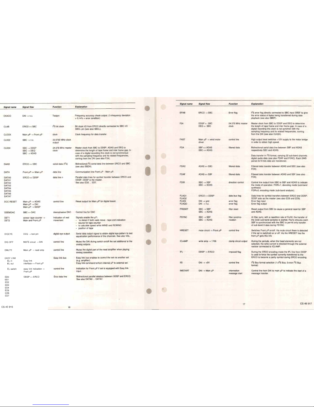
CS45916
16
17
CS45917
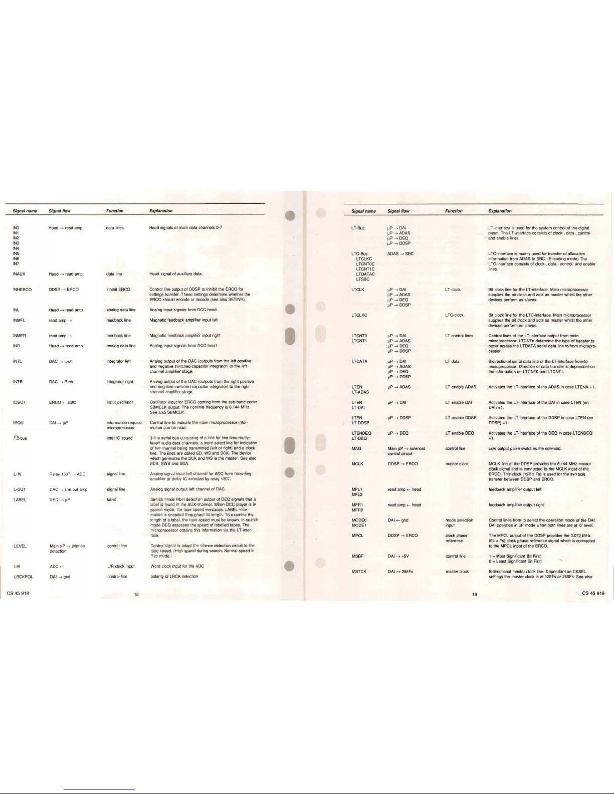
Signal name Signalflow Function
Explanation
Signal name
Signal flow Function Explanation
INO
Head~read amp data lines
Head signals of main data channels 0-7
LT-Bus
).lP~DAI
LT-interface is used for the system control of the digital
IN1
).lP~ADAS panel. The LT-interface consists of clock-, data-, control-
IN2
).lP~DEQ and enable lines.
IN3
).lP~DDSP
IN4
IN5
LTC-Bus ADAS
~
SBC
LTC-interface
is
mainly used for transfer of allocation
IN6
LTCLKC
information from ADAS to SBC. (Encoding mode) The
IN7
LTCNTOC
LTC-interface consists of
c1ock-,
data-, control- and enable
LTCNT1C lines.
INAUX
Head
~
read amp data line
Head signal of auxiliary data.
LTDATAC
LTSBC
INHERCO DDSP
~
ERCO
inhibit ERCO
Control line output of DDSP to inhibit the ERCO for
LTCLK
).lP~DAI
LT-c1ock
Bit clock line for the LT-interface. Main microprocessor
settings transfer. These settings determine whether the
).lP~ADAS supplies the bit clock and acts as master whilst the other
ERCO should encode or decode (see also SETINH).
).lP~DEQ devices perform as slaves.
).lP~DDSP
INL Head
~
read amp
analog data line
Analog input signals from DCC head
LTCLKC
LTC-clock
Bit clock line for the LTC-interface. Main microprocessor
INMFL read amp
~
feedback line
Magnetic feedback amplifier input left
supplies the bit clock and acts as master whilst the other
devices perform as slaves.
INMFR read amp
~
feedback line
Magnetic feedback amplifier input right
LTCNTO
).lP~
DAI
LT control lines Control lines of the LT-interface output from main
LTCNT1
).lP~ADAS
microprocessor. LTCNTn determine the type of transfer to
INR Head
~
read amp analog data line
Analog input signals from DCC head
).lP~DEQ occur across the LTDATA serial data line tolfrom micropro-
).lP~DDSP cessor.
INTL DAC
~
L-ch
integrator left
Analog output of the DAC
(ou1puts
from the left positive
LTDATA
).lP~DAI
LT data Bidirectional serial data line of the LT-interface fromlto
and negative switched-capacitor integrator) to the left
).lP
~ADAS
microprocessor. Direction of data transferisdependant on
channel amplifier stage.
).lP~DEQ the information on L
TCNTO
and LTCNT1 .
).lP~DDSP
INTR DAC
~
R-ch
integrator right
Analog output of the DAC (outputs from the right positive
and negative switched-capacitor integrator) to the right
LTEN
).lP~ADAS L
Tenable
ADAS Activates the LT-interface of the ADAS in case LTENA =1.
channel amplifier stage.
LT-ADAS
IOSC1
ERCO <- SBC
input oscillator
Oscillator input for ERCO coming from the sub-band coder
LTEN
).lP~
DAI
L
Tenable
DAI Activates the LT-interface of the DAI in case LTEN (on
SBMCLK output. The nominal frequency is 6.144 MHz.
LT-DAI DAI) =1.
See also SBMCLK.
LTEN
).lP~DDSP
L
Tenable
DDSP Activates the LT-interface of the DDSP in case LTEN
(on
IRQU
DAI
~).lP
information request
Control line to indicate the main microprocessor infor-
LT-DDSP DDSP) =1.
microprocessor
mation can
be
read.
LTENDEQ
).lP~DEQ L
Tenable
DEQ Activates the LT-interface of the DEQ in case LTENDEQ
1
2
S-bus
inter
IC
sound
3-line serial bus consisting of a line for two time-multip-
•
LT-DEQ
=1
.
lexed audio data channels, a word select line for indication
of the channel being transmitted (left or right) and a clock
MAG Main
).lP~solenoid control line Low output pulse switches the solenoid.
line. The lines are called SD,
WS
and SCK. The device
control circuit
which generates the SCK and WS is the master. See also
SCK, SWS and SDA.
MCLK DDSP
~
ERCO masterclock MCLK line of the DDSP provides the 6.144 MHz master
clock signal and is connected
to
the MCLK input of the
L-IN Relay 1307
~
ADC
signal line
Analog signal input left channel for ADC from recording
ERCO. This clock (128 x Fs) is used for the symbols
amplifier or dolby
IC
selected by relay 1307.
transfer between DDSP and ERCO.
L-OUT DAC~line out amp
signal line
Analog signal output left channel of DAC.
MFL1
read amp <- head feedback amplifier output left
MFL2
LABEL
DEQ~
).lP
label
Search mode label detection output of DEQ signals that a
label is found in the AUX-channel. When DCC player
is
in
MFR1
read amp <- head
feedback amplifier output right
search mode, the tape speed increases. LABEL infor-
MFR2
mation is encoded throughout its length. To examine the
length of a label, the tape speed must
be
known.Insearch
MODEO
DAI <- gnd mode selection Control lines from to select the operation mode of the DAI.
mode DEQ assesses the speed of labelled tapes. The
MODE1
input
DAI
operatesin).lP
mode when both lines are at '0' level.
microprocessor obtains this information via the LT-inter-
face.
MPCL DDSP
~
ERCO clock phase The MPCL output of the DDSP provides the 3.072 MHz
reference (64 x Fs) clock phase reference signal which is connected
LEVEL Main
).lP~silence
control line
Control signal
to
adapt the silence detection circuit to the
to the MPCL input of the ERCO.
detection
tape speed. (High speed during search, Normal speed in
Rec mode.)
MSBF DAI
~
+5V
control line
1 = Most Significant Bit First
o= Least Significant Bit First
UR
ADC <-
UR
clock input Word clock input for the ADC
MSTCK
DAI
.....
256Fs master clock Bidirectional master clock line. DependantonCKSEL
LRCKPOL DAI
~
gnd
control line
polarity of LRCK selection
settings the master clock
is
at 128Fs or 256Fs. See also
CS45918
18
19
CS45919
 Loading...