

PHILIPS 50PUG6504/78, 58PUD6654/43, 50PUG6504/77, 58PUD6654/44, 50PUD6504/77 Service manual & schematics
...
TPM19.6L
LA
Chassis name Platform Model name
50PUG6504/78 58PUD6654/43
50PUG6504/77 58PUD6654/44
50PUD6504/77 58PUD6654/54
50PUD6654/43 58PUD6654/55
50PUD6654/44 58PUD6654/77
50PUD6654/54 58PUG6654/78
50PUD6654/55 58PUT6654/57
50PUD6654/77 65PUD6654/43
50PUG6654/78 65PUD6654/44
TPM19.6L LA MTK5806
50PUT6654/57 65PUG6654/78
55PUD6654/43 65PUD6794/43
55PUD6654/44 65PUD6794/44
55PUD6654/77 65PUD6794/54
55PUG6654/78 65PUD6794/77
55PUD6794/43 65PUG6794/78
55PUD6794/44 65PUD6794/57
55PUD6794/54 65PUT6794/57
55PUD6794/77 75PUD6754/55
55PUT6794/57 75PUD6754/77
55PUG6794/78
Published by Doris /SC 2029 Quality Subject to modification 3122 785 21011
2019 © TP Vision Netherlands B.V.
All rights reserved. Specifications are subject to change without notice. Trademarks are the
property of Koninklijke Philips Electronics N.V. or their respective owners.
TP Vision Netherlands B.V. reserves the right to change products at any time without being obliged to adjust
earlier supplies accordingly.
PHILIPS and the PHILIPS’ Shield Emblem are used under license from Koninklijke Philips Electronics N.V.
2020-Jul-17

1. Product information……….…………………………………………………………………………………4
2. Precautions, Notes, and Abbreviation List…………….………………………………………………6
3. Mechanical Instructions………………….……………………………………………………………….12
Cable dressing (50" 6504 series)……………………………………………………………………12
Cable dressing (50" 6654 series)…………………………………………………………………13
Cable dressing (58" 6654 series)…………………………………………………………………14
Cable dressing (55"/65" 6794 series)………………………………………………………………14
Assembly/Panel Removal …………………………………………………………………………………16
4. Service Modes…………….……………….……………….…………………………………………….….20
5. Software upgrading, Error Code and Set Option Code……...…………………………………..24
6. Trouble Shooting……………………………………………...……………………………………………..28
7. Electrical Diagram…..………………….………………………………………………………………31
8. IC Data Sheet……...……………………………………………………………………………….…..35
9. Circuit Diagrams…………..…………………………………………………………………………….37
9.1 715GA018 PSU…………………………………………………………………..……………………37
9.2 715GA052 PSU…………………………………………………………………..……………………41
9.3 715G9856 PSU…………………………………………………………………..……………………45
9.4 715G9907 SSB…………………………………………………………………..……………………49
9.5 715G8623 IR/LED Panel…………………………………………..…………………………………69
9.6 715GA039 IR/LED Panel…………………………………………..…………………………………70
9.7 715G9740 Keyboard control panel…………………………………………………………………….71
9.8 715GA032 AMBI Panel……………………………………………..……………………………….72
9.9 715GA033 AMBI Panel…………………………………………………..………………………….74
9.10 715G9946 AMBI Panel…………………………………………………..………………………….76
9.11 715GA030 AMBI Panel…………………………………………………..………………………….78
9.12 715GA034 AMBI Panel…………………………………………………..………………………….80
10. Styling Sheet……………….……………………………………………………………………………..82
6 50 4 s er ie s 5 0" …… …… .. …… …… …… …… …… …… …… …… …… …… …… …… .8 2
6 65 4 s er ie s 5 0" …… …… .. …… …… …… …… …… …… …… …… …… …… …… …… .8 3
6 65 4 s er ie s 5 8" …… …… .. …… …… …… …… …… …… …… …… …… …… …… …… .8 4
6 79 4 s er ie s 5 5" …… …… .. …… …… …… …… …… …… …… …… …… …… …… …… .8 5
6 79 4 s er ie s 6 5" …… …… .. …… …… …… …… …… …… …… …… …… …… …… …… .8 6
Published by Doris /SC 2029 Quality Subject to modification 3122 785 21011
2019 © TP Vision Netherlands B.V.
All rights reserved. Specifications are subject to change without notice. Trademarks are the
property of Koninklijke Philips Electronics N.V. or their respective owners.
TP Vision Netherlands B.V. reserves the right to change products at any time without being obliged to adjust
earlier supplies accordingly.
PHILIPS and the PHILIPS’ Shield Emblem are used under license from Koninklijke Philips Electronics N.V.
2020-Jul-17

1. Product information
Product specifications are subject to change without notice.
For more specification details of this product, see
www.philips.com/TVsupport
Display Resolution
Diagonal screen size
50PUx6xx4: 126cm/50inch
55PUx6xx4: 139cm/55inch
58PUx6xx4: 146cm/58inch
65PUx6xx4: 164cm/65inch
75PUx6xx4: 189cm/75inch
Display resolution
3840 x 2160
Support Timing
Video support timing also includes field/frame rate
23.976Hz, 29.97Hz and 59.94Hz.
HDMI
480i
480p
576i
576p
720p-50Hz, 60Hz
1080i-50Hz, 60Hz
1080p-50Hz, 60Hz
3840 x 2160p– 24Hz, 25Hz, 30Hz, 50Hz, 60Hz
HDMI - UHD
(HOME) > Settings > General settings > Input
source > HDMI(port) >HDMI Ultra HD
(50Hz or 60Hz) RGB 4:4:4 or YCbCr 4:4:4/4:2:2/4:2:0
signals.
• The setting Standard allows maximum up to Ultra HD
(50Hz or 60Hz) YCbCr 4:2:0 signals.
Component, Composite
Composite
PAL,NTSC,SECAM
Supported Input Resolution – Computer
640 x 480 – 60Hz
800 x 600 – 60Hz
1024 x 768 – 60Hz
1280 x 800 – 60Hz
1280 x 960 – 60Hz
1280 x 1024 – 60Hz
1366 x 768 – 60Hz
1440 x 900 – 60Hz
1920 x 1080 – 60Hz
3840 x 2160 – 60Hz
Note: For HDMI Input only
Reception
• Aerial input : 75 ohm coaxial (F-type)
• Tuner bands : Hyperband, ISDB-T, UHF, VHF
• ISDB-T
• Analogue video playback : PAL
• Digital video playback : MPEG2 SD/HD (ISO/IEC
13818-2), MPEG4 SD/HD (ISO/IEC 14496-10), HEVC*
• Digital audio playback (ISO/IEC 13818-3)
This TV can display Ultra HD signals. Some devices –
connected with HDMI – do not recognize a TV with Ultra
HD and might not work correctly or show distorted picture
or sound.
To avoid the malfunctioning of such a device, you can set
the signal quality to a level the device can handle. If the
device is not using Ultra HD signals, you can switch off
Ultra HD for this HDMI connection.
• The setting Optimal* allows maximum up to Ultra HD
Sound
• Dolby Atmos® Virtualizer
• Clear Dialogue
• A.I Sound
• 5 Band Equalizer
• Output power (RMS) : 20W
• Dolby® Audio
• DTS-HD

Connectivity
TV Side
• CVBS: CVBS, Audio L/R
• USB 2 - USB 3.0
• HDMI 3 in - UHD - HDR
• Headphones - Stereo mini-jack 3.5mm
TV Bottom
• Digital Audio out: Optical
• USB 1 - USB 2.0
• Network LAN - RJ45
• SERV.U - "SERV.U" is used by customer service to
troubleshoot any faults.
• Antenna (75 ohm)
• HDMI 1 in - ARC – UHD-HDR
• HDMI 2 in - UHD - HDR
Power
• Mains power : AC 110-240V +/-10%
• Ambient temperature : 5°C to 35°C

2. Precautions, Notes, and Abbreviation List
tools. This will prevent any short circuits and the danger
of a circuit becoming unstable.
2.1 Safety Instructions
Safety regulations require the following during a repair:
• Connect the set to the Mains/AC Power via an isolation
transformer (> 800 VA).
• Replace safety components, indicated by the symbol △!,
only by components identical to the original ones. Any
other component substitution (other than original type)
may increase risk of fire or electrical shock hazard.
Safety regulations require that after a repair, the set must
be returned in its original condition. Pay in particular
attention to the following points:
• Route the wire trees correctly and fix them with the
mounted cable clamps.
• Check the insulation of the Mains/AC Power lead for
external damage.
• Check the strain relief of the Mains/AC Power cord for
proper function.
• Check the electrical DC resistance between the
Mains/AC Power plug and the secondary side (only for
sets that have a Mains/AC Power isolated power supply):
1. Unplug the Mains/AC Power cord and connect a wire
between the two pins of the Mains/AC Power plug.
2. Set the Mains/AC Power switch to the “on” position
(keep the Mains/AC Power cord unplugged!).
3. Measure the resistance value between the pins of the
Mains/AC Power plug and the metal shielding of the
tuner or the aerial connection on the set. The reading
should be between 4.5 MΩ and 12 MΩ.
4. Switch “off” the set, and remove the wire between the
two pins of the Mains/AC Power plug.
• Check the cabinet for defects, to prevent touching of any
inner parts by the customer.
!
2.2 Warnings
• All ICs and many other semiconductors are susceptible
to electrostatic discharges (ESD ). Careless handling
during repair can reduce life drastically. Make sure that,
during repair, you are connected with the same potential
as the mass of the set by a wristband with resistance.
Keep components and tools also at this same potential.
• Be careful during measurements in the high voltage
section.
• Never replace modules or other components while the
unit is switched “on”.
• When you align the set, use plastic rather than metal
2.3 Notes
2.3.1 General
• Measure the voltages and waveforms with regard to the
chassis (= tuner) ground ( ), or hot ground ( ),
depending on the tested area of circuitry. The voltages
and waveforms shown in the diagrams are indicative.
Measure them in the Service Default Mode with a colour
bar signal and stereo sound (L: 3 kHz, R: 1 kHz unless
stated otherwise) and picture carrier at 475.25 MHz for
PAL, or 61.25 MHz for NTSC (channel 3).
• Where necessary, measure the waveforms and voltages
with ( ) and without ( ) aerial signal. Measure the
voltages in the power supply section both in normal
operation ( ) and in stand-by ( ). These values are
indicated by means of the appropriate symbols.
2.3.2 Schematic Notes
• All resistor values are in ohms, and the value multiplier is
often used to indicate the decimal point location (e.g.
2K2 indicates 2.2 kΩ).
• Resistor values with no multiplier may be indicated with
either an “E” or an “R” (e.g. 220E or 220R indicates 220
Ω).
• All capacitor values are given in micro-farads (µ = x10-6),
nano-farads (n = x10-9), or pico-farads (p = x10
• Capacitor values may also use the value multiplier as the
decimal point indication (e.g. 2p2 indicates 2.2 pF).
• An “asterisk” (*) indicates component usage varies.
Refer to the diversity tables for the correct values.
• The correct component values are listed on the Philips
Spare Parts Web Portal.
2.3.3 Spare parts
For the latest spare part overview, consult your Philips
Spare Part web portal.
2.3.4 BGA (Ball Grid Array) ICs
Introduction
For more information on how to handle BGA devices, visit
this URL: http://www.atyourservice-magazine.com. Select
“Magazine”, then go to “Repair downloads”. Here you will
find Information on how to deal with BGA-ICs.
BGA Temperature Profiles
For BGA-ICs, you must use the correct temperature-profile.
Where applicable and available, this profile is added to the
-12
).

IC Data Sheet information section in this manual.
2.3.5 Lead-free Soldering
Due to lead-free technology some rules have to be
respected by the workshop during a repair:
• Use only lead-free soldering tin. If lead-free solder paste
is required, please contact the manufacturer of your
soldering equipment. In general, use of solder paste
within workshops should be avoided because paste is
not easy to store and to handle.
• Use only adequate solder tools applicable for lead-free
soldering tin. The solder tool must be able:
– To reach a solder-tip temperature of at least 400°C.
– To stabilize the adjusted temperature at the solder-tip.
– To exchange solder-tips for different applications.
• Adjust your solder tool so that a temperature of around
360°C - 380°C is reached and stabilized at the solder
joint. Heating time of the solder-joint should not exceed ~
4 sec. Avoid temperatures above 400°C, otherwise
wear-out of tips will increase drastically and flux-fluid will
be destroyed. To avoid wear-out of tips, switch “off”
unused equipment or reduce heat.
• Mix of lead-free soldering tin/parts with leaded soldering
tin/parts is possible but PHILIPS recommends strongly to
avoid mixed regimes. If this cannot be avoided, carefully
clear the solder-joint from old tin and re-solder with new
tin.
For the third digit, the numbers 1...9 and the characters
A...Z can be used, so in total: 9 plus 26= 35 different
B.O.M.s can be indicated by the third digit of the serial
number.
Identification: The bottom line of a type plate gives a
14-digit serial number. Digits 1 and 2 refer to the production
centre (e.g. SN is Lysomice, RJ is Kobierzyce), digit 3
refers to the B.O.M. code, digit 4 refers to the Service
version change code, digits 5 and 6 refer to the production
year, and digits 7 and 8 refer to production week (in
example below it is 2010 week 10 / 2010 week 17). The 6
last digits contain the serial number.
2.3.6 Alternative BOM identification
It should be noted that on the European Service website,
“Alternative BOM” is referred to as “Design variant”.
The third digit in the serial number (example:
AG2B0335000001) indicates the number of the alternative
B.O.M. (Bill Of Materials) that has been used for producing
the specific TV set. In general, it is possible that the same
TV model on the market is produced with e.g. two different
types of displays, coming from two different suppliers. This
will then result in sets which have the same CTN
(Commercial Type Number; e.g. 28PW9515/12) but which
have a different B.O.M. number.
By looking at the third digit of the serial number, one can
identify which B.O.M. is used for the TV set he is working
with. If the third digit of the serial number contains the
number “1” (example: AG1B033500001), then the TV set
has been manufactured according to B.O.M. number 1. If
the third digit is a “2” (example: AG2B0335000001), then
the set has been produced according to B.O.M. no. 2. This
is important for ordering the correct spare parts!
Figure 3-1 Serial number (example)
2.3.7 Board Level Repair (BLR) or Component Level
Repair (CLR)
If a board is defective, consult your repair procedure to
decide if the board has to be exchanged or if it should be
repaired on component level.
If your repair procedure says the board should be
exchanged completely, do not solder on the defective board.
Otherwise, it cannot be returned to the O.E.M. supplier for
back charging!
2.3.8 Practical Service Precautions
• It makes sense to avoid exposure to electrical shock.
While some sources are expected to have a possible
dangerous impact, others of quite high potential are of
limited current and are sometimes held in less regard.

• Always respect voltages. While some may not be
dangerous in themselves, they can cause unexpected
reactions that are best avoided. Before reaching into a
powered TV set, it is best to test the high voltage
insulation. It is easy to do, and is a good service
precaution.
2.4 Abbreviation List
0/6/12 SCART switch control signal on A/V board.
0 = loop through (AUX to TV),6 = play 16 :
9 format, 12 = play 4 : 3 format
DNR Digital Noise Reduction: noise reduction
feature of the set
AARA Automatic Aspect Ratio Adaptation:
algorithm that adapts aspect ratio to
remove horizontal black bars; keeps the
original aspect ratio
ACI Automatic Channel Installation: algorithm
that installs TV channels directly from a
cable network by means of a predefined
TXT page
ADC Analogue to Digital Converter
AFC Automatic Frequency Control: control
signal used to tune to the correct
frequency
AGC Automatic Gain Control: algorithm that
ontrols the video input of the feature box
AM Amplitude Modulation
AP Asia Pacific
AR Aspect Ratio: 4 by 3 or 16 by 9
ASF Auto Screen Fit: algorithm that adapts
aspect ratio to remove horizontal black
bars without discarding video information
ATSC Advanced Television Systems Committee,
the digital TV standard in the USA
ATV See Auto TV
Auto TV A hardware and software control system
that measures picture content, and adapts
image parameters in a dynamic way
AV External Audio Video
AVC Audio Video Controller
AVIP Audio Video Input Processor
B/G Monochrome TV system. Sound carrier
distance is 5.5 MHz
BDS Business Display Solutions (iTV)
BLR Board-Level Repair
BTSC Broadcast Television Standard Committee.
Multiplex FM stereo sound system,
originating from the USA and used e.g. in
LATAM and AP-NTSC countries
B-TXT Blue TeleteXT
C Centre channel (audio)
CEC Consumer Electronics Control bus: remote
control bus on HDMI connections
CL Constant Level: audio output to connect
with an external amplifier
CLR Component Level Repair
ComPair Computer aided rePair
CP Connected Planet / Copy Protection
CSM Customer Service Mode
CTI Color Transient Improvement: manipulates
steepness of chroma transients
CVBS Composite Video Blanking and
Synchronization
DAC Digital to Analogue Converter
DBE Dynamic Bass Enhancement: extra low
frequency amplification
DCM Data Communication Module. Also
referred to as System Card or Smartcard
(for iTV).
DDC See “E-DDC”
D/K Monochrome TV system. Sound carrier
distance is 6.5 MHz
DFI Dynamic Frame Insertion
DFU Directions For Use: owner's manual
DMR Digital Media Reader: card reader
DMSD Digital Multi Standard Decoding
DNM Digital Natural Motion
DRAM Dynamic RAM
DRM Digital Rights Management
DSP Digital Signal Processing
DST Dealer Service Tool: special remote control
designed for service technicians
DTCP Digital Transmission Content Protection; A
protocol for protecting digital audio/video
content that is traversing a high speed
serial bus, such as IEEE-1394
DVB-C Digital Video Broadcast - Cable
DVB-T Digital Video Broadcast - Terrestrial
DVD Digital Versatile Disc
DVI(-d) Digital Visual Interface (d= digital only)
E-DDC Enhanced Display Data Channel (VESA
standard for communication channel and
display). Using E-DDC, the video source
can read the EDID information form the
display.

EDID Extended Display Identification Data
(VESA standard)
EEPROM Electrically Erasable and Programmable
Read Only Memory
EMI Electro Magnetic Interference
EPG Electronic Program Guide
EPLD Erasable Programmable Logic Device
EU Europe
EXT EXTernal (source), entering the set by
SCART or by cinches (jacks)
FDS Full Dual Screen (same as FDW)
FDW Full Dual Window (same as FDS)
FLASH FLASH memory
FM Field Memory or Frequency Modulation
FPGA Field-Programmable Gate Array
FTV Flat TeleVision
Gb/s Giga bits per second
G-TXT Green TeleteXT
H H_sync to the module
HD High Definition
HDD Hard Disk Drive
HDCP High-bandwidth Digital Content Protection:
A “key” encoded into the HDMI/DVI signal
that prevents video data piracy. If a source
is HDCP coded and connected via
HDMI/DVI without the proper HDCP
decoding, the picture is put into a “snow
vision” mode or changed to a low
resolution. For normal content distribution
the source and the display device must be
enabled for HDCP “software key”
decoding.
HDMI High Definition Multimedia Interface
HP HeadPhone
I Monochrome TV system. Sound carrier
distance is 6.0 MHz
I2C Inter IC bus
I2D Inter IC Data bus
I2S Inter IC Sound bus
IF Intermediate Frequency
IR Infra Red
IRQ Interrupt Request
ITU-656 The ITU Radio communication Sector
(ITU-R) is a standards body subcommittee
of the International Telecommunication
Union relating to radio communication.
ITU-656 (a.k.a. SDI), is a digitized video
format used for broadcast grade video.
Uncompressed digital component or digital
composite signals can be used. The SDI
signal is self-synchronizing, uses 8 bit or
10 bit data words, and has a maximum
data rate of 270 Mbit/s, with a minimum
bandwidth of 135 MHz.
iTV Institutional TeleVision; TV sets for hotels,
hospitals etc.
LS Last Status; The settings last chosen by
the customer and read and stored in RAM
or in the NVM. They are called at start-up
of the set to configure it according to the
customer's preferences
LATAM Latin America
LCD Liquid Crystal Display
LED Light Emitting Diode
L/L' Monochrome TV system. Sound carrier
distance is 6.5 MHz. L' is Band I, L is all
bands except for Band I
LPL LG.Philips LCD (supplier)
LS Loudspeaker
LVDS Low Voltage Differential Signalling
Mbps Mega bits per second
M/N Monochrome TV system. Sound carrier
distance is 4.5 MHz
MHEG Part of a set of international standards
related to the presentation of multimedia
information, standardised by the
Multimedia and Hypermedia Experts
Group. It is commonly used as a language
to describe interactive television services
MIPS Microprocessor without Interlocked
Pipeline-Stages; A RISC-based
microprocessor
MOP Matrix Output Processor
MOSFET Metal Oxide Silicon Field Effect Transistor,
switching device
MPEG Motion Pictures Experts Group
MPIF Multi Platform InterFace
MUTE MUTE Line
MTV Mainstream TV: TV-mode with Consumer
TV features enabled (iTV)
NC Not Connected
NICAM Near Instantaneous Compounded Audio
Multiplexing. This is a digital sound system,
mainly used in Europe.
NTC Negative Temperature Coefficient,
non-linear resistor

NTSC National Television Standard Committee.
Color system mainly used in North
America and Japan. Color carrier NTSC
M/N= 3.579545 MHz, NTSC 4.43=
4.433619 MHz (this is a VCR norm, it is
not transmitted off-air)
NVM Non-Volatile Memory: IC containing TV
related data such as alignments
O/C Open Circuit
OSD On Screen Display
OAD Over the Air Download. Method of
software upgrade via RF transmission.
Upgrade software is broadcasted in TS
with TV channels.
OTC On screen display Teletext and Control;
also called Artistic (SAA5800)
P50 Project 50: communication protocol
between TV and peripherals
PAL Phase Alternating Line. Color system
mainly used in West Europe (colour carrier
= 4.433619 MHz) and South America
(colour carrier PAL M = 3.575612 MHz and
PAL N = 3.582056 MHz)
PCB Printed Circuit Board (same as “PWB”)
PCM Pulse Code Modulation
PDP Plasma Display Panel
PFC Power Factor Corrector (or
Pre-conditioner)
PIP Picture In Picture
PLL Phase Locked Loop. Used for e.g. FST
tuning systems. The customer can give
directly the desired frequency
POD Point Of Deployment: a removable CAM
module, implementing the CA system for a
host (e.g. a TV-set)
POR Power On Reset, signal to reset the uP
PSDL Power Supply for Direct view LED
backlight with 2D-dimming
PSL Power Supply with integrated LED drivers
PSLS Power Supply with integrated LED drivers
with added Scanning functionality
PTC Positive Temperature Coefficient,
non-linear resistor
PWB Printed Wiring Board (same as “PCB”)
PWM Pulse Width Modulation
QRC Quasi Resonant Converter
QTNR Quality Temporal Noise Reduction
QVCP Quality Video Composition Processor
RAM Random Access Memory
RGB Red, Green, and Blue. The primary color
signals for TV. By mixing levels of R, G,
and B, all colors (Y/C) are reproduced.
RC Remote Control
RC5 / RC6 Signal protocol from the remote control
receiver
RESET RESET signal
ROM Read Only Memory
RSDS Reduced Swing Differential Signalling data
interface
R-TXT Red TeleteXT
SAM Service Alignment Mode
S/C Short Circuit
SCART Syndicat des Constructeurs d'Appareils
Radiorécepteurs et Téléviseurs
SCL Serial Clock I2C
SCL-F CLock Signal on Fast I2C bus
SD Standard Definition
SDA Serial Data I2C
SDA-F DAta Signal on Fast I2C bus
SDI Serial Digital Interface, see “ITU-656”
SDRAM Synchronous DRAM
SECAM SEequence Couleur Avec Mémoire.
Colour system mainly used in France and
East Europe. Colour carriers = 4.406250
MHz and 4.250000 MHz
SIF Sound Intermediate Frequency
SMPS Switched Mode Power Supply
SoC System on Chip
SOG Sync On Green
SOPS Self Oscillating Power Supply
SPI Serial Peripheral Interface bus; a 4-wire
synchronous serial data link standard
S/PDIF Sony Philips Digital InterFace
SRAM Static RAM
SRP Service Reference Protocol
SSB Small Signal Board
SSC Spread Spectrum Clocking, used to
reduce the effects of EMI
STB Set Top Box
STBY STand-BY
SVGA 800 × 600 (4:3)
SVHS Super Video Home System
SW Software
SWAN Spatial temporal Weighted Averaging
Noise reduction
SXGA 1280 × 1024

TFT Thin Film Transistor
THD Total Harmonic Distortion
TMDS Transmission Minimized Differential
Signalling
TS Transport Stream
TXT TeleteXT
TXT-DW Dual Window with TeleteXT
UI User Interface
uP Microprocessor
UXGA 1600 × 1200 (4:3)
V V-sync to the module
VESA Video Electronics Standards Association
VGA 640 × 480 (4:3)
VL Variable Level out: processed audio output
toward external amplifier
VSB Vestigial Side Band; modulation method
WYSIWYR What You See Is What You Record: record
selection that follows main picture and
sound
WXGA 1280 × 768 (15:9)
XTAL Quartz crystal
XGA 1024 × 768 (4:3)
Y Luminance signal
Y/C Luminance (Y) and Chrominance (C)
signal
YPbPr Component video. Luminance and scaled
color difference signals (B-Y and R-Y)
YUV Component video

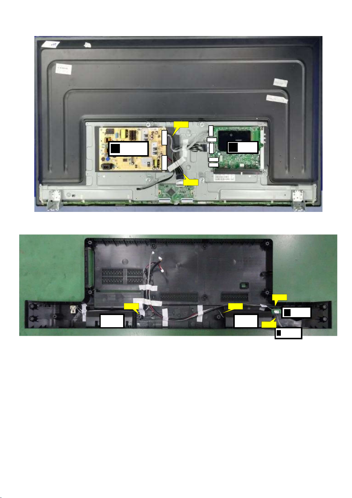
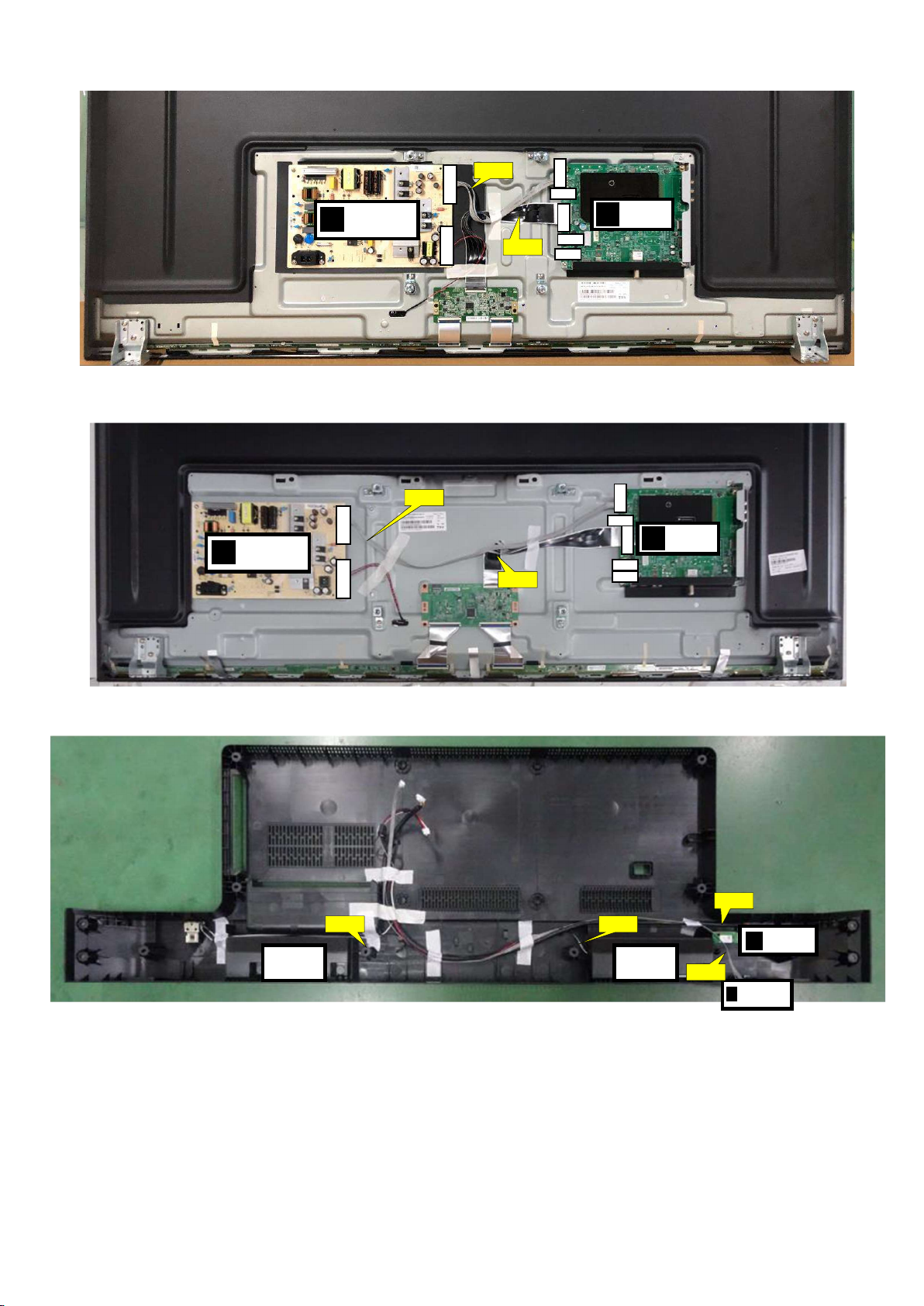
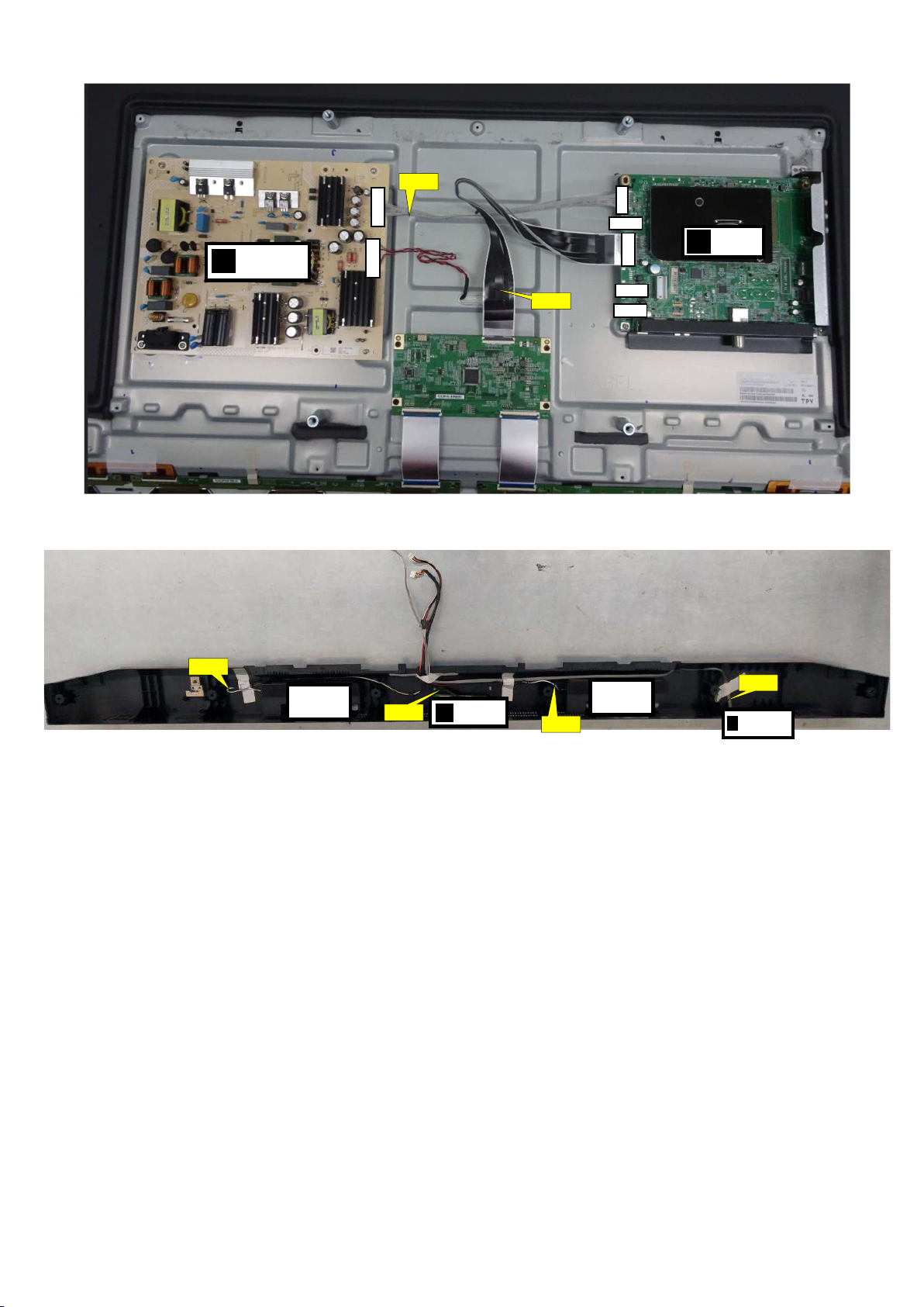
3. Mechanical Instructions
ECN
601
408
CN701
8601
(1054)
ECN
701
LOUDSPEAKER
W
CN9102
ECN
408
ECN
415 ECN
601
ECN
401
E
J
ECN
401
LOUDSPEAKER
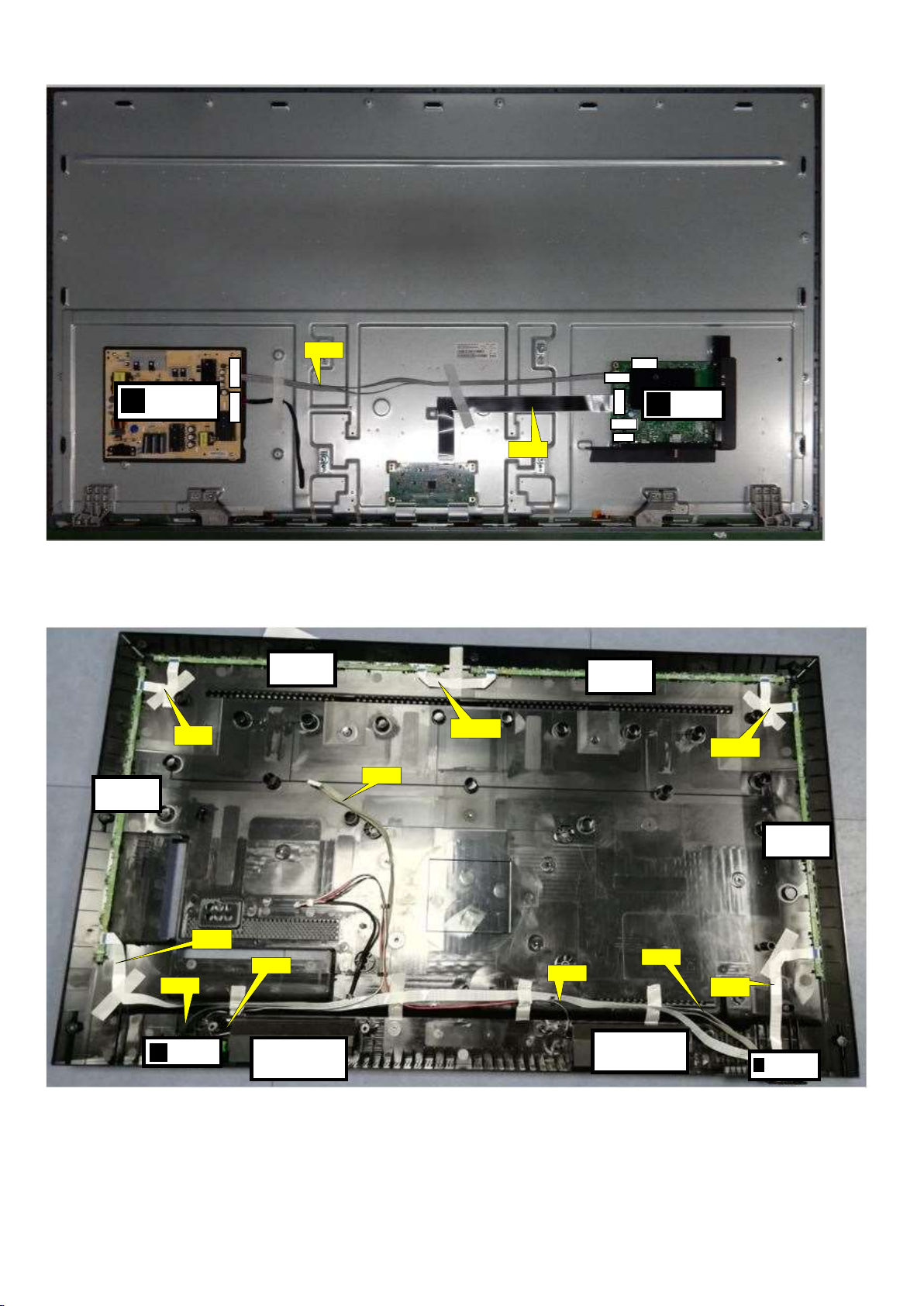
3.1 Cable Dressing
MAIN POWER SUPPLY
A
CN401
CN
CN
CN601
CN415
SSB(1053)
B
(1184)
Cable dressing (50" 6504 series)
Back cover overview (50" 6504 series)
(1184)
WIFI MODULE
(Wifi02)
IR/LED BOARD
(1056)
KEY BOARD
(1057)
ECN
601
CN
408
CN701
CN
860
2
(1054)
ECN
701
(1184)
W
CN9101
ECN
408
ECN
415
ECN
601
J
CN
401
ECN
401
(1184)
A
LOUDSPEAKER
MAIN POWER SUPPLY
Cable dressing (50" 6654 series)
SSB (1053)
B
CN601
CN415
WIFI MODULE
LOUDSPEAKER
(Wifi02)
Back cover overview (50" 6654 series)
IR/LED BOARD
(1056)
ECN
601
408
CN701
(1054)
ECN
701
(1184)
W
CN
415
ECN
408 ECN
415
ECN
601
J
ECN
401
(1184)
CN
860
1
CN
9102
CN
408
CN701
(1054)
ECN
701
601
ECN
408
CN
401
CN
860
2
9102
CN
MAIN POWER SUPPLY
A
CN
CN415
B
SSB (1053)
Cable dressing (55" 6654 series)
CN401
CN
SSB (1053)
MAIN POWER SUPPLY
A
B
CN601
Cable dressing (58" 6654 series)
WIFI MODULE
LOUDSPEAKER
LOUDSPEAKER
(Wifi02)
IR/LED BOARD
(1056)
Back cover overview (55”/58" 6654 series)
ECN
601
408
CN701
(1054)
ECN
701
W
CN415
ECN
408
ECN
415
ECN
601
J
CN401
ECN
401
1
9102
CN
MAIN POWER SUPPLY
A
CN860
Cable dressing (65" 6654 series)
CN
CN601
B
SSB (1053)
LOUDSPEAKER
(1184)
WIFI MODULE
(Wifi02)
LOUDSPEAKER
(1184)
IR/LED BOARD
(1056)
Back cover overview (65" 6654 series)
701
CN
408
CN
601
9102
MAIN POWER SUPPLY
(1054)
ECN
701
ECN
408
CN
8601
(1184)
W
ECN
416
ECN
415
ECN
601
ECN
601
E
XA04-1
(1184)
ECN416
J
A
CN416
CN
CN
SSB (1053)
B
CN415
Ambilight
(1061)
EXA04
ECN03
Ambilight
(1061)
Cable dressing (55”/65” 6794 series)
Ambilight
(1062)
EXA04-2
Ambilight
(1061)
ECN02
WIFI MODULE
(Wifi02)
LOUDSPEAKER
LOUDSPEAKER
IR/LED BOARD
(1056)
Back cover overview (55" 6794 series)

W ECN
416
ECN
415 ECN
601
ECN
601
ECN02
Ambilight
J
E
XA04-3 EXA04-2
E
XA04-4
(1063)
Ambilight
(1062)
Ambilight
(1063)
EXA04-1
Ambilight
(1061)
EXA04-5
Ambilight
(1061)
ECN03
WIFI MODULE
(Wifi02)
3.2 Assembly/Panel Removal
LOUDSPEAKER
(1184)
ECN03
LOUDSPEAKER
(1184)
Back cover overview (65" 6794 series)
EXA04
IR/LED BOARD
(1056)
Ambilight
(1061)
Ambilight
(1061)
3.2.1 IR board Control Unit
1. Unplug the connector from the SSB.
Caution: be careful, as these are very fragile connectors!
2. Remove fixation screws [1] and connector [2] from the IR board control unit.
3. Remove the IR lens, IR board from the DECO_REAR_COVER.
When defective, replace the whole unit.
1
2

3.2.2 Stand removal
1. Remove the fixation screws [1] that secure the stand.
2. Take the stand bracket out from the set.
(43"50" 6504 series)
1
(65x4/67x4 Series)
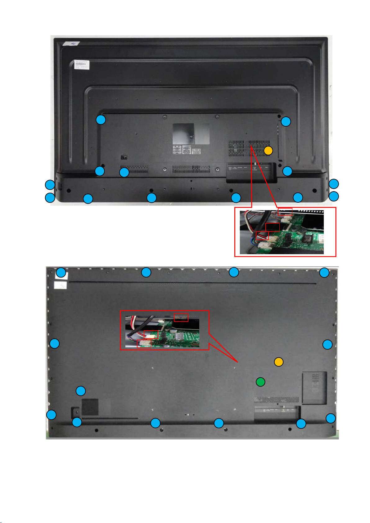
3.2.3 Rear Cover
Warning: Disconnect the mains power cord before removing the rear cover.
1. Remove all fixation screws [1] ,[2]and [3] that secure the Back cover assy.
2. Unplug the connector that marked by red box below from SSB.
3. Gently lift the rear cover from the TV. Make sure that wires and cables are not damaged while lifting the rear cover from the set.
1
2
2
2
2
2
2
2
2
2
1
2
2
2
2
2
(65x4 series)
2
2
2
2
2
2
2
2
2
3.2.4 Keyboard Control Unit
1. Release the connector from the SSB Board.
Caution: be careful, the Keyboard is catch on the Back cover, please be careful to avoid damage the fragile connectors!
2. Remove all the fixation screws from the keyboard control panel [2] and take it out from the Back cover.
2
(67x4 series)
1
3
2
2

1
When defective, replace the whole unit.
2
2
(6504 series)
3.2.5 Small Signal Board (SSB)
Caution: it is mandatory to remount all different screws at their original position during re-assembly. Failure to do so may result in damaging the SSB.
1. Release the clips from the LVDS connector that connect with the SSB[1].
Caution: be careful, as these are very fragile connectors!
2. Unplug all other connectors [2] .
3. Remove all the fixation screws from the SSB [3].
4. The SSB can now be shifted from side connector cover, then lifted and taken out of the I/O bracket.
3
3
2
3
3.2.6 Power Supply Unit (PSU)
Caution: it is mandatory to remount all different screws at their original position during re-assembly. Failure to do so may result in damaging the PSU.
1. Gently unplug all connectors from the PSU.
2. Remove all fixation screws from the PSU.
3. The PSU can be taken out of the set now.
3
3.2.7 Speakers
1. Gently release the tapes that secure the speaker cables.
2. Unplug the speaker connector from the SSB.
3. Take the speakers out.
When defective, replace the both units.
3.2.8 WIFI module
1. Unplug the connector from the SSB.

2. Remove fixation screw that secure the WIFI module.
When defective, replace the whole unit.
3.2.9 LCD Panel
1. Remove the SSB as described earlier.
2. Remove the PSU as described earlier.
3. Remove the keyboard control panel as described earlier.
4. Remove the stand bracket as described earlier.
5. Remove the IR/LED as described earlier.
6. Remove the fixations screws that fix the metal clamps to the front bezel. Take out those clamps.
7. Remove all other metal parts not belonging to the panel.
8. Lift the LCD Panel from the bezel.
When defective, replace the whole unit.

4. Service Modes
4.1 Service Modes
The Service Mode feature is split into following parts:
Service Alignment Mode (SAM).
Factory Mode.
Customer Service Mode (CSM).SAM and the Factory mode offer features, which can be used by the Service engineer to repair/align a TV set.
SAM and the Factory mode offer features, which can be used by the Service engineer to repair/align a TV set. Some features are:
Make alignments (e.g. White Tone), reset the error buffer(SAM and Factory Mode).
Display information (“SAM” indication in upper right corner of screen, error buffer, software version, operating hours,options and option codes, sub
menus).
The CSM is a Service Mode that can be enabled by the consumer. The CSM displays diagnosis information, which the customer can forward to the dealer
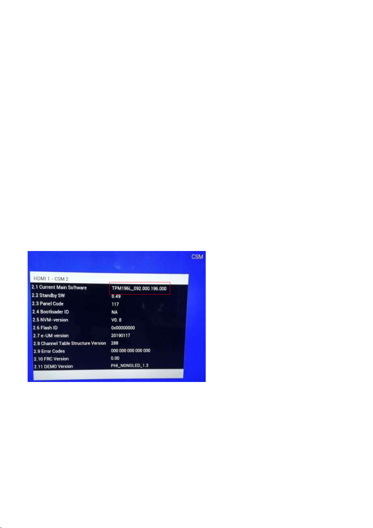
or call centre. In CSM mode, “CSM”, is displayed in the top right corner of the screen. The information provided in CSM and the purpose of CSM is to:
Increase the home repair hit rate.
Decrease the number of nuisance calls.
Solved customers’ problem without home visit.
Note: For the new model range, a new remote control (RC) is used with some renamed buttons. This has an impact on the activation of the Service modes.
For instance the old “MENU” button is now called “HOME” (or is indicated by a “house” icon).
4.2 Service Alignment Mode (SAM)
Purpose
To modify the NVM.
To display/clear the error code buffer.
To perform alignments.
Specifications
Operation hours counter (maximum five digits displayed).
Software version, error codes, and option settings display.
Error buffer clearing.
Option settings.
Software alignments (White Tone).
NVM Editor.
Set screen mode to full screen (all content is visible).
How to Activate SAM
To activate SAM, use one of the following methods:
Press the following key sequence on the remote control transmitter: “062596”, directly followed by the “INFO/OK” button. Do not allow the
display to time out between entries while keying the sequence.
Or via ComPair.
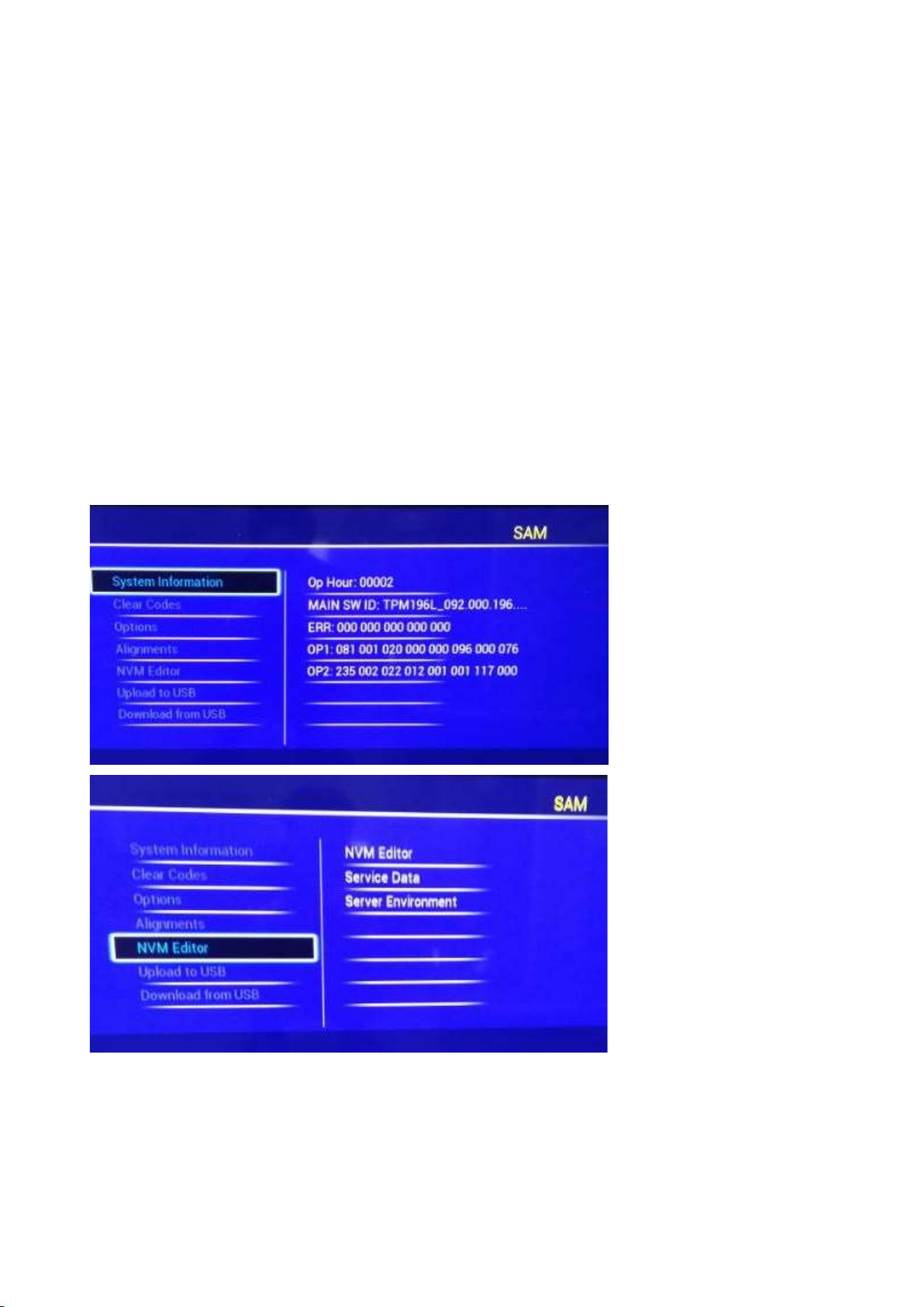
After entering SAM, the following items are displayed,
with “SAM” in the upper right corner of the screen to indicate that the television is in Service Alignment Mode.
How to Navigate
In the SAM menu, select menu items with the UP/DOWN keys on the remote control transmitter. The selected item will be indicated. When not
all menu items fit on the screen, use the UP/DOWN keys to display the next/previous menu items.
With the “LEFT/RIGHT” keys, it is possible to:
– (De) activate the selected menu item.
– (De) activate the selected sub menu.
– Change the value of the selected menu item.
When you press the MENU button once while in top level SAM, the set will switch to the normal user menu (with the SAM mode still active in the
background).
How to Store SAM Settings
To store the settings changed in SAM mode (except the RGB Align settings), leave the top level SAM menu by using the POWER button on the
remote control transmitter or the television set. The mentioned exceptions must be stored separately via the STORE button.
How to Exit SAM
Use one of the following methods:
Switch the set to STANDBY by pressing the mains button on the remote control transmitter or the television set.
Via a standard RC-transmitter, key in “00” sequence.
Note: When the TV is switched “off” by a power interrupt while in SAM, the TV will show up in “normal operation mode” as soon as the power is
supplied again. The error buffer will not be cleared.
SAM mode overview
Remark: Under main menu “NVM editor”, select “Service Data”, you can use the UP/DOWN keys to view and change the set Type number, the set
Production Number or the 18AC of a part.(The NVM-editor still has the same function as before, alpha-numeric entry.)
4.3 Factory mode:
Purpose
To perform extended alignments.

Specifications
Displaying and or changing Panel ID information.
Displaying and or changing Tuner ID information.
Error buffer clearing.
Various software alignment settings.
Testpattern displaying.
Public Broadcasting Service password Reset.
etc.
How to Activate the Factory mode
To activate the Factory mode, use the following method:
Press the following key sequence on the remote control transmitter: from the “menu/home” press “1999”, directly followed by the
“Back/Return” button. Do not allow the display to time out between entries while keying the sequence.
After entering the Factory mode, we can see many items displayed, use the UP/DOWN keys to display the next/previous menu items
Factory mode overview
How to Exit the Factory mode
Select EXIT_FACTORY from the menu and press the “OK” button.
Note: When the TV is switched “off” by a power interrupt, or normal switch to “stand-by” while in the factory mode, the TV will show up in “normal
operation mode” as soon as the power is supplied again. The error buffer will not be cleared.
4.4 Customer Service Mode (CSM)
Purpose
The Customer Service Mode shows error codes and information on the TVs operation settings.The call centre can instruct the customer (by
telephone) to enter CSM in order to identify the status of the set.This helps the call centre to diagnose problems and failures in the TV set before
making a service call.
The CSM is a read-only mode; therefore, modifications are not possible in this mode.
Specifications
Ignore “Service unfriendly modes”.
Line number for every
line (to make CSM language independent).
Set the screen mode to full
screen (all contents on screen is visible).
After leaving the Customer Service Mode, the original settings are restored.
Possibility to use “CH+” or “CH-” for channel surfing, or enter the specific channel number on the RC.

How to Activate CSM
To activate CSM, press the following key sequence on a standard remote control transmitter: “123654” (do not allow the display to time out
between entries while keying the sequence). After entering the Customer Service Mode, the following items are displayed. use the Right/Left keys
to display the next/previous menu items
Note: Activation of the CSM is only possible if there is no (user) menu on the screen!
CSM Overview
How to Navigate
By means of the “CURSOR-DOWN/UP” knob (or the scroll wheel) on the RC-transmitter, can be navigated through the menus.
How to Exit CSM
To exit CSM, use one of the following methods.
Press the MENU/HOME button on the remote control transmitter.
Press the POWER button on the remote control transmitter.
Press the POWER button on the television set.
5. Software Upgrading, Error code and Panel Code
5.1 Software Upgrading
5.1.1. The following update is for .pkg file.
1. Rename the file to “upgrade_loader.pkg”.
2. Prepare a USB memory (File format: FLAT, Size: 1G~8G).
3. Copy the software to USB flash disk (root directory).
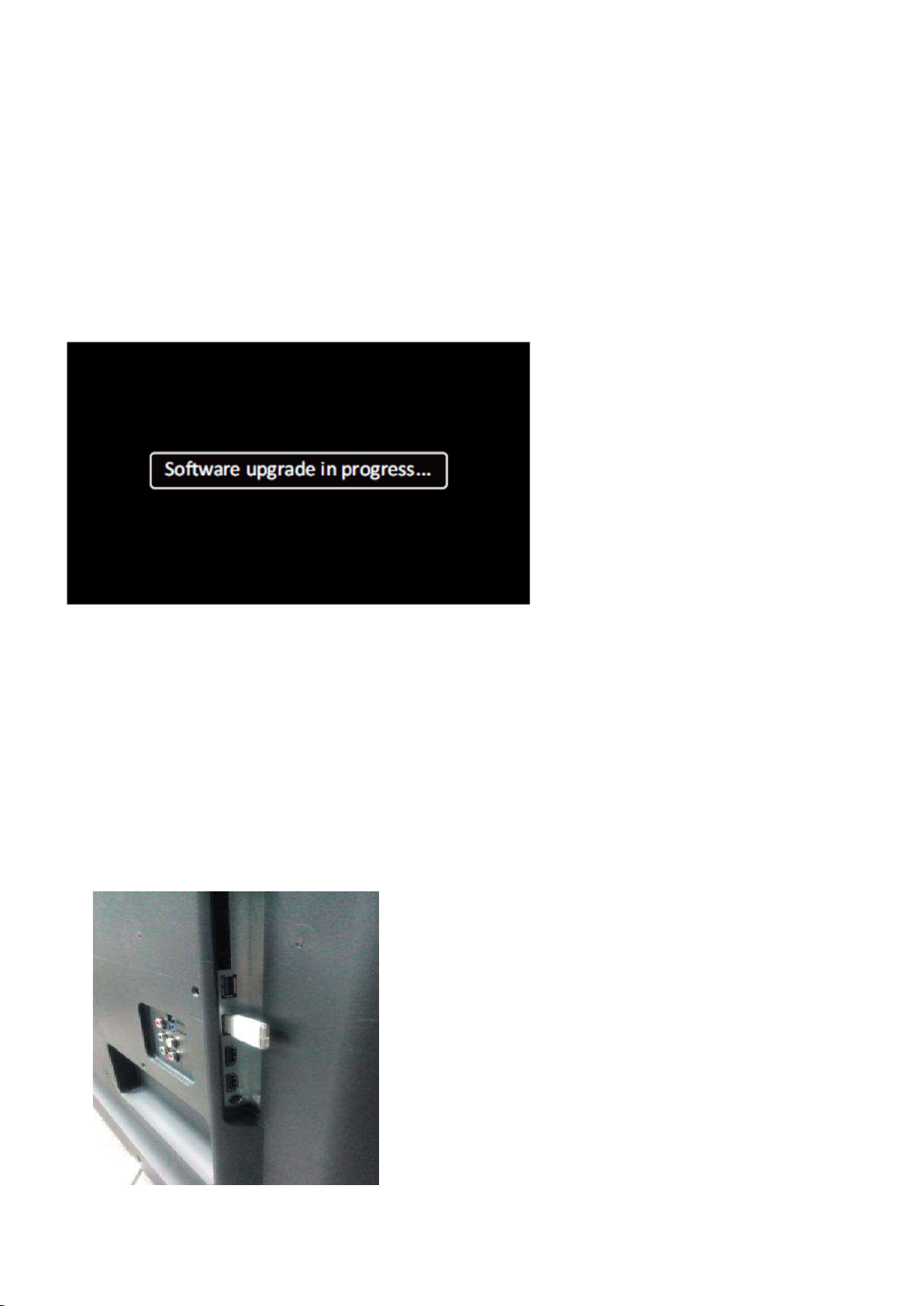
4. Switch off the TV and Insert the USB memory stick that contains the software update files in one of the TV’s USB 2.0 port.
Note: It contains USB3.0 port, if connect on it, the software may can’t be detected.
5. Switch on the TV. The TV will detect the USB memory s tick automatically. Then a window jumps out as below:
6. When the TV software is updated, the TV will turn on again automatically. Remove your USB flash drive.
7. We can enter in CSM or Factory mode to check the current software version.
5.1.2. The following update is for .upg file.
Step 1: Ready for F/W Upgrade
1. Rename the file to “autorun.upg”.
2. Prepare a USB memory (File format: FLAT, Size: 1G~8G).
3. Copy the software to USB flash disk (root directory).
4. Switch on the TV and Insert the USB memory stick that contains the software update files in one of the TV’s USB 2.0 port.
Note the version of this F/W before you change the software file name.
Step 2: F/W Upgrade
Warning:
Do not switch off your TV or remove your USB flash drive during the software update.
If a power failure occurs during the update, do not remove your USB flash drive from your TV. Your TV will continue the update as soon as power is
restored.
If an error occurs during the update, retry the procedure. If the error reoccurs, contact Philips Consumer Care
1. Connect your USB flash drive (containing the software update) to the USB connector on the TV. Wait 30 seconds or until
the USB drive is recognized by the TV.
2. Your TV will start loading the software automatically.
3. When the loading of the software finished, press “Start” to activate the upgrade of the TV.
Notes:
If the USB flash drive is not detected, disconnect it and reconnect again.
In case the software does not start loading automatically, you can also update the software manually
1. Press (Settings) on your remote control, and select All Settings > Update Software > Local Updates, and press OK.
2. Select the software file and follow the on-screen instruction to install latest software on your TV.
Step 3: Check the SW version
1. After burning software, TV will restart
2. Press “123654”, enter Customer Service Mode to check if the software version is correct.
Caution: Please make sure that software upgrade is finished before unplug the USB and AC power!
5.2 Error Code
5.2.1 Introduction
Error codes are required to indicate failures in the TV set. In principle a unique error code is available for every:
• Activated (SW) protection.
• Failing I2C device.
• General I2C error.
The last five errors, stored in the NVM, are shown in the Service menu’s. This is called the error buffer.
The error code buffer contains all errors detected since the last time the buffer was erased. The buffer is written from left to right. When an error occurs that
is not yet in the error code buffer, it is displayed at the left side and all other errors shift one position to the right.
An error will be added to the buffer if this error differs from any error in the buffer. The last found error is displayed on the left.

An error with a designated error code never leads to a deadlock situation. It must always be diagnosable (e.g. error buffer via OSD or blinking LED).
In case a failure identified by an error code automatically results in other error codes (cause and effect), only the error code of the MAIN failure is displayed.
5.2.2 How to Read the Error Buffer
You can read the error buffer in following ways:
• On screen via the SAM/CSM (if you have a picture).
Example:
– ERROR: 000 000 000 000 000: No errors detected
– ERROR: 013 000 000 000 000: Error code 13 is the last and only detected error
– ERROR: 034 013 000 000 000: Error code 13 was detected first and error code 34 is the last detected (newest) error
• Via the blinking LED procedure (when you have no picture).
5.2.3 Error codes overview
In this chassis only “layer 2” error codes are available and point to problems on the SSB. They are triggered by LED blinking
when CSM is activated. Only the following layer 2 errors are defined:
5.2.4 How to Clear the Error Buffer
The error code buffer is cleared in the following cases:
• By using the CLEAR command in the SAM menu

50PUD6504/77
TPT500B5
-
U1T01DS04RXYTPV
TBD 58PUD6654/44
TPT580B5
-
U1T01.DS01RXYTPV
138
50PUD6654/43
TPT500B5
-
GT024.HS12AXYTPV
161 58PUD6654/54
TPT580B5
-
U1T01.DS01ACXYTPV
TBD 50PUD6654/44
TPT500B5
-
GT024.HS12AXYTPV
161 58PUD6654/54
TPT580B5
-
U1T01.DS01RXYTPV
138 50PUD6654/54
TPT500B5
-
GT024.HS12AXYTPV
161 58PUD6654/55
TPT580B5
-
U1T01.DS01ACXYTPV
TBD
50PUD6654/77
TPT500B5
-
GT024.HS12AXYTPV
161 58PUD6654/55
TPT580B5
-
U1T01.DS01RXYTPV
138
50PUD6654/77
TPT500B5
-
U2T01.DS01APXYTPV
TBD 58PUD6654/77
TPT580B5
-
U1T01.DS01ABXYTPV
TBD 50PUG6654/78
TPT500B5
-
GT024.HS12AXYTPV
161 58PUD6654/77
TPT580B5
-
U1T01.DS01RXYTPV
138 50PUG6654/78
TPT500B5
-
U2T01.DS01APXYTPV
TBD 58PUD6654/77
TPT580F2
-
PV5D.QS01KXY
TPV 162
50PUG6654/78
TPT500
-
PV5D.QS01BXYTPV
155 58PUG6654/78
TPT580B5
-
U1T01.DS01ABXYTPV
TBD 50PUG6654/78
TPT500
-
PV5D.QS01HXYTPV
TBD 58PUG6654/78
TPT580B5
-
U1T01.DS01RXYTPV
138 50PUT6654/57
TPT500B5
-
GT024.HS12AXYTPV
161 58PUG6654/78
TPT580F2
-
PV5D.QS01KXYTPV
162 55PUD6654/43
TPT550J1
-
QUBF84.KS89P0HXMTPV
TBD 58PUT6654/57
TPT580B5
-
U1T01.DS01RXYTPV
138
55PUD6654/44
TPT550J1
-
QUBF84.KS89P0HXMTPV
TBD 58PUT6654/57
TPT580F2
-
PV5D.QS01KXYTPV
162
55PUD6654/77
TPT550J1
-
QUBF84.KS89P0HXMTPV
TBD 65PUD6794/43
TPT650J1
-
QUBF70.KSDWP0HXMTPV
159
55PUD6654/77
TPT550J1
-
QUBF84.KS89P0UXMTPV
TBD 65PUD6794/43
TPT650J1
-
QUBF90.K9WP0LXMTPV
TBD 55PUD6794/43
TPT550J1
-
QUBH84.KSD9P0PXMTPV
123 65PUD6794/44
TPT650J1
-
QUBF70.KSDWP0HXMTPV
159
55PUD6794/44
TPT550J1
-
QUBH84.KSD9P0PXMTPV
123 65PUD6794/44
TPT650J1
-
QUBF90.K9WP0LXMTPV
TBD
55PUD6794/54
TPT550J1
-
QUBH84.KSD9P0PXMTPV
123 65PUD6794/54
TPT650J1
-
QUBF70.KSDWP0HXMTPV
159
55PUD6794/77
TPT550J1
-
QUBH84.KSD9P0PXMTPV
123 65PUD6794/54
TPT650J1
-
QUBF90.K9WP0LXMTPV
TBD
55PUG6654/78
TPT550J1
-
QUBF84.KS89P0HXMTPV
TBD 65PUD6794/77
TPT650J1
-
QUBF70.KSDWP0HXMTPV
159
55PUG6654/78
TPT550J1
-
QUBF84.KS89P
0UXMTPV
TBD 65PUD6794/77
TPT650J1
-
QUBF90.K9WP0LXMTPV
TBD
55PUG6794/78
TPT550J1
-
QUBH84.KSD9P0BCXMTPV
TBD 65PUD6794/77
TPT650J1
-
QUBF90.K9WP1AJXMTPV
TBD
55PUG6794/78
TPT550J1
-
QUBH84.KSD9P0PXMTPV
123 65PUG6794/78
TPT650J1
-
QUBF70.KSDWP0HXMTPV
159
55PUG6794/78
TPT550J1
-
QUBF70.KSNWP1HXMTPV
163 65PUG6794/78
TPT650J1
-
QUBF90.K9WP0LXMTPV
TBD
55PUT6794/57
TPT550J1
-
QUBH84.KSD9P0PXMTPV
123 65PUT6794/57
TPT650J1
-
QUBF70.KSDWP0HXMTPV
159
55PUT6794/57
TPT550J1
-
QUBF70.KSNWP1HXMTPV
163 65PUT6794/57
TPT650J1
-
QUBF90.K9WP0LXMTPV
TBD 58PUD6654/43
TPT580B5
-
U1T01.DS01ACXYTPV
TBD 75PUD6754/55
TPT750UA
-
QUBN9D.KSD830CXMTPV
TBD
58PUD6654/43
TPT580B5
-
U1T01.DS01RXYTPV
138 75PUD6754/77
TPT750UA
-
QUBN9D.KS98P2CXMTPV
TBD
58PUD6654/44
TPT580B5
-
U1T01.DS01ACXYTPV
TBD
• By using the CLEAR command in the Factory mode:
• By using the following key sequence on the remote control transmitter: “062599” directly followed by the OK button.
• If the contents of the error buffer have not changed for 50 hours, the error buffer resets automatically.
Note: If you exit SAM by disconnecting the mains from the television set, the error buffer is not reset.
5.3 Set Option Code
Press the following key sequence on a standard RC transmitter: “062598” directly followed by MENU and “xxx”, where “xxx” is a 3 digit decimal value
of the panel type: see column “Set Option Code” in below tab. After resetting the Display Code, restart the set immediately.
CTN_ALT
BOM#
Panel Type
Set
Option
Code
CTN_ALT
BOM#
Panel Type
Set
Option
Code

Trouble shooting
Picture-related
2016年12月10日
2016/4/8
Ask Photo
SW
issue
N
Intermittent
problem ?
Y
Y
SW latest ?
N
Update SW
N
Problem
solved ?
Y
Finish
Y
Picture ?
N
Backlight?
N
LED working ?
Y
Sound ?
SW+SSB
Y
N
PSU/SSB
Y
PSU+ Panel
Menu Smarkt
function?
N
SSB+LVDS+Panel
RAM
Y
Signal
issue

Trouble shooting
Audio/Sound-
related
2016年12月10日
2016/4/8
HW
issue
SW
N
Intermittent
problem ?
Y
Y
SW latest ?
N
Update SW
N
Problem
solved ?
Y
Finish
Y
Sound ?
N
Mute ?
N
Extra device
connect?
N
Factory
setting
Sound back ? Setting issue
N
Y
Y
Check extra
Y
device
Setting
issue
SSB+SPK

Trouble shooting system
N
Smart
function
issue ?
N
Intermittent
problem ?
Remark2:
Y
Y
2016年4月11日
2016/12/11
System related
Remark1:
Y
TV start
up ?
N
Network
connect ?
N
Connect network
Y
SW latest ?
N
Update SW
Problem
solved ?
Y
Y
N
SW issue
Commerce way
SCC
available ?
Y
Execute
SCC
Problem
solved ?
Y
N
N
SW update
available ?
Y
SW update
N
Problem
Y
solved ?
N
HW repair
Remark1 : What is System related issue ?
1.Permanent reboots
2.Intermittent reboots
3.No function, no standby LED (set dead)
4.No function, blinking LED
5.Set freezes, intermittently
6.Slow response to user interaction
7.Switches ON by itself
8.Switches Off by itself
9.Stuck in standby mode / unable to start up
10.Stuck on PHILIPS / ANDROID logo
11.CAM not recognized by TV
12.CAM authentication issue
13.Misc CAM issue
14.IP-EPG issues
15.BC-EPG issues
16.PVR issues w/ BC-EPG
17.PVR issues w/ IP-EPG
18.PVR issues / generic
19.EDFU-related issue
20.Features not available in UI / cannot be activated
Remark2 : How to judge intermittent issue ?
1.When the problem happened can be solved by:
1)AC off AC on
2)DC off DC on
3)RC switch different source
2.The problem intermittent happened
Finish
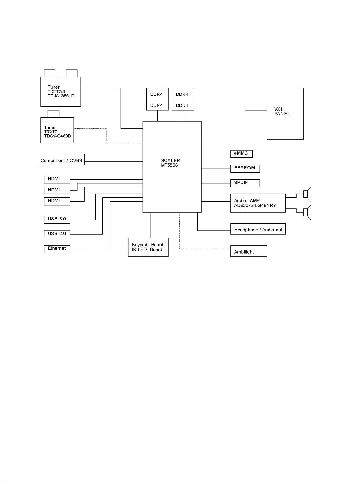
7. Electrical Diagram
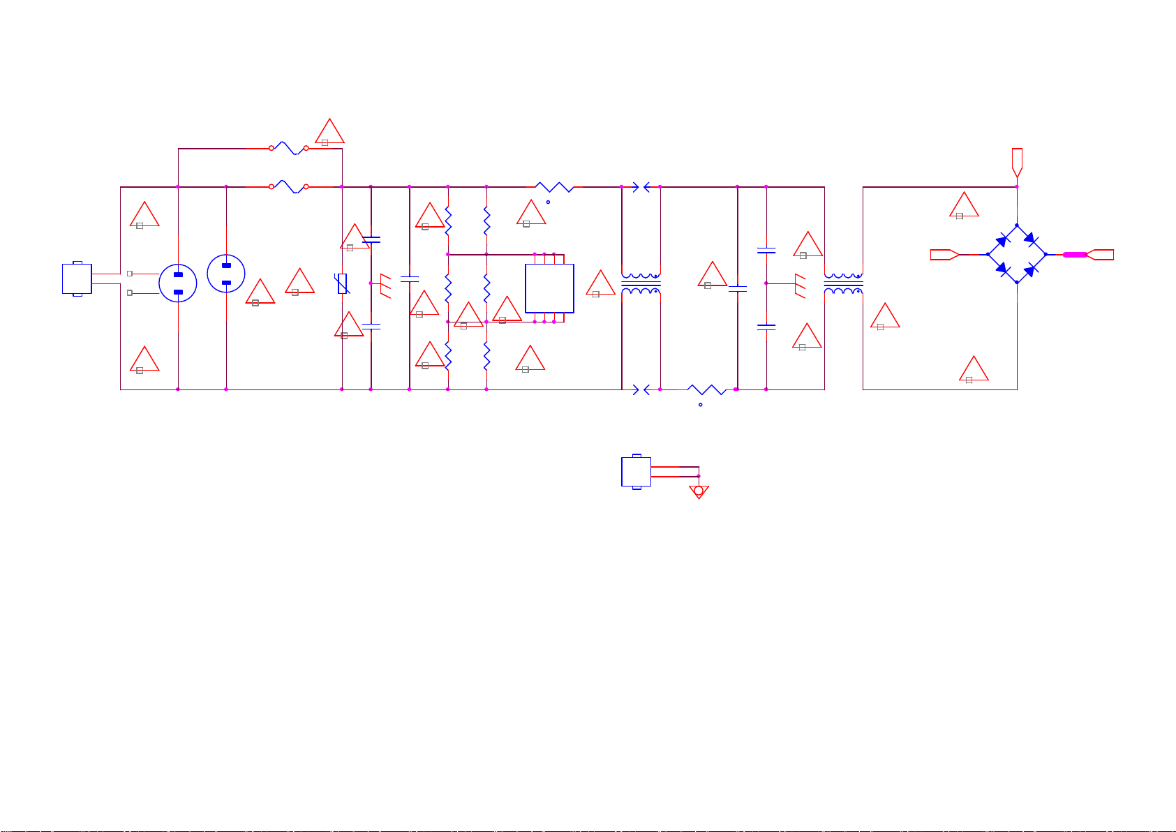
7.1 Block diagram
7.2 Power Supply
CN
701
AUDIO
AMP
Main filter
Power architecture of this platform.
LVDS
12V
12V
7.3 Power tree
Display power
CN8601
PFC
Platform power
DIM
ON/OFF
PS_ON
12V
12V_A
AC-input +
AC IN
Platform
MT5806

7.4 Power layout SSB
C789 +12V PANEL
R703, +5V_STB
R577, +5V_SW
C250, Main_12V
C111, +5V_USB
Power SSB Top View

R769, DVDD3V3
C128, +3V3_TUNER
Power SSB Bottom View

8. IC Data Sheets
8.1 MT5806HFEQ (IC U401--Scaler)

8.2 AD82072-LG48NRY (IC U601--Audio)

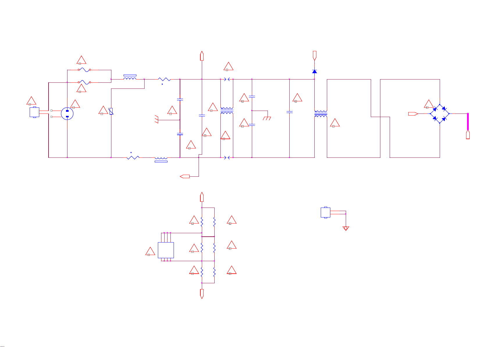
9.Circuit Diagrams
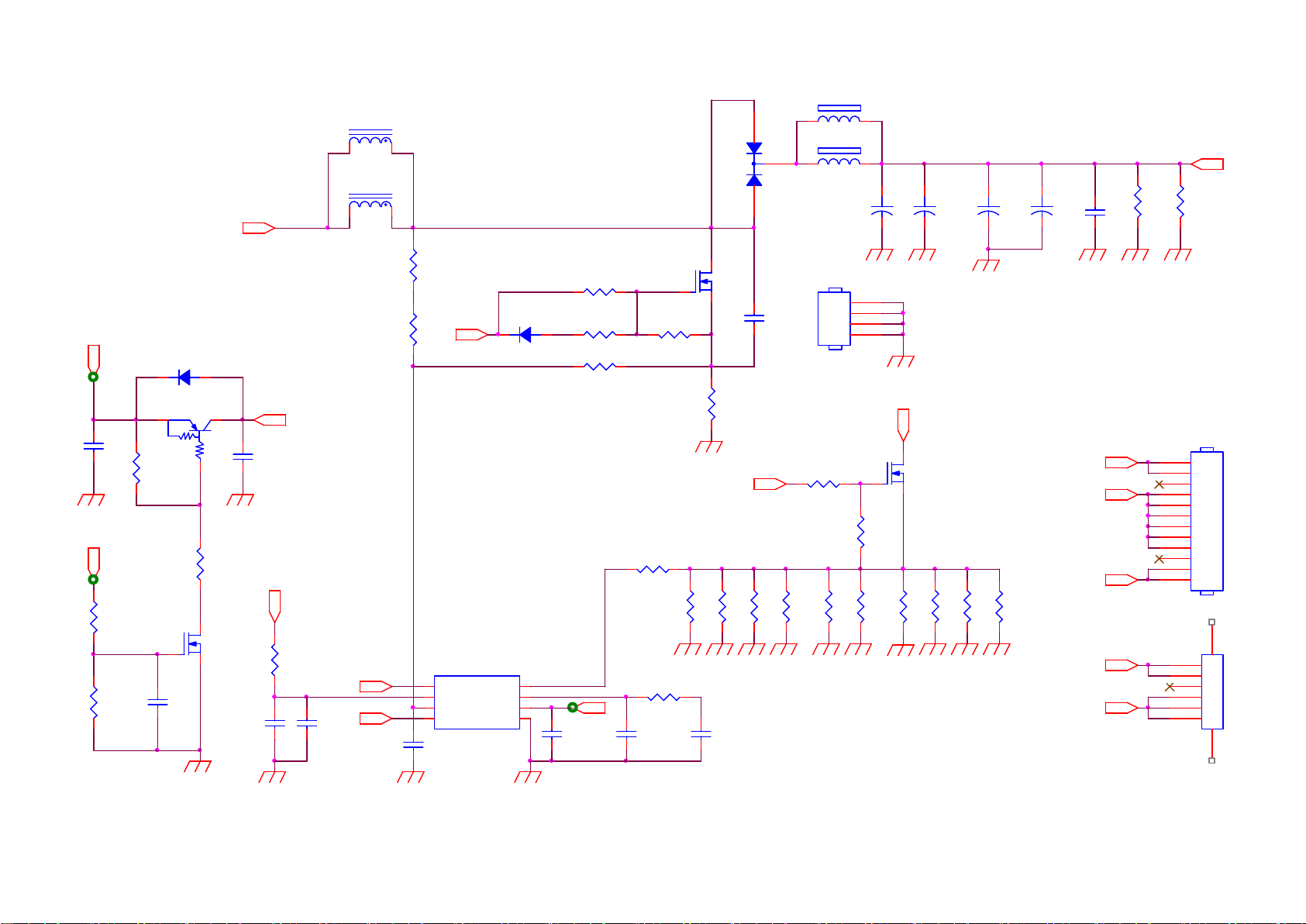
9.1 A 715GA018 PSU(For 55”/65” 6794 & 65” 6654 Series)
9-1-1 AC Input
12
F9901
5A 250V
!
CN9901
AC 2P
!
T5A H / 2 5 0V
!
RV9901
1
2
3
L9904
0.25mH
680V
!
4
NC/ GND1
1
GND
!
NC/ GND2
1
C9901
470NF 275V
2
1
GND
!
C9911
220PF 250V
!
C9912
220PF 250V
NC/ GND3
1
SG9901
DSPL-501N-A21F
!
1
L9902
4
17mH
SG9902
DSPL-501N-A21F
GND
!
C9913
470PF 250V
3
!
2
!
C9902
470NF 275V
3
1
4
L9903
17mH
2
3
12
NR9902
1.5R
BR
t
12
t
NR9901
1.5R
!
C9914
470PF 250V
D9901
PG4007
!
4
NR9904
NTCR 2R5
NR9905
NTCR 2R5
C9904
NC/ 100PF 500V
C9903
NC/ 100PF 500V
-
2
1
+
BD9901
TS10P06G-05
U9901
CAP200DG-TL
1D12D13NC4
NC
NC5D26D27NC
8
FB9901
BEAD
1 2
! !
R9903
750K
!
R9905
NC/ 750K
!
R9901
750K
Rsen-
2
R9904
750K
!
R9906
NC/ 750K
!
R9902
750K
Vsin
FB9904
127R
!
For B D 99 0 1
NC/ HEAT SINK
1
2
3
4
GND
1 2
C9915
1000PF/1500PF 250V
HS9901
1

9-1-2 PFC with LD7592S
Vsin
Rsen-
PFC_VCC
R9819
0 OHM 5% 1/8W
4
!
C9804
1uF 450V
HVvcc
C9805
NC/ 47PF
5
E1
1
L9801
240uH
4
3
GND
!
6
L9802
1
NC/ 170uH
R9803
33 OHM 1/4W
D9805
SS1060FL
D9804
SS1060FL
R9802
47OHM
Q9803
MMBT2907A
Q9801
TK13A60D
1
R9805
10KOHM
D9801
FMNS-1106S
2
3
C9817
100pF 2KV
C9806
1000pF
GND
C9818
2.2NF
C9819
NC/ 1000pF
+
C9801
47UF 450V
GND
+
C9802
47UF 450V
+
C9803
NC/ 47UF 450V
R9804
1.5M 1%
R9806
1.5M 1%
GND
GND
R9808
0R05
R9809
NC/ 0R05
For Q9 8 01 D 9 8 01
HV
+
C9808
10uF 50V
GND
C9815
0.1uF 50V
12K 1/10W 1%
C9810
470pF 50V
GND
R9813
GND
8
INV1RAMP2COMP3CS
6
OUT7VCC
5
U9801
LD7592
OVP
GND
4
10K 1/10W 1%
R9814
C9812
47nF 10% 50V
GND
GND
C9813
470NF 10% 25V
GND
R9801
18K 1%
R9899
2.7K 1%
R9818
NC/ 0R05
Q9802
MTN127KN3
R9811
1K OHM 1%
HS9801
HEAT SIN K
1
2
3
4
GND
R9817
10K 1/4W
NC
C9814
ZD9801
100pF 50V
1 2
GND
R9816
100K 1/10W 1%
PFC_VCC

9-1-3 LLC with SSC3S927
HV
ADJ
PFC_VCC
100K 1%
R9166
ZD9152
BZT52-B16
C9101
1000pF 2KV
GND
C9104
10NF
1N4148W
D9102
1 2
GND
Q9105
BTC4672M3
GND
0R05 1/4W
R9168
2Kohm
R9103
36K OHM
R9105
200R
R9165
C9102
2.2NF
510K
STB
R9104
C9105
0.22UF
C9107
220pF 50V
C9179
NC/0.22U F
C9180
220NF
R9102
0R05 1/4W
R9106
120R
Q9106
MMBT3906
FB_LLC
C9106
0.47UF 50V
CL
VCC1
R9113
100K
R9112
100K 1%
R9101
3M 1%
C9121
0.01uF 100V
Q9107
LMBT3904LT1G
R9111
10K 1%
LLC_OVP
R9167
200K 1%
C9118
0.47uf
Q9108
MMBT3906
C9109
10NF 10% 50V
R9100
3M 1%
1
2
3
4
5
6
7
8
C9110
4.7NF
REG
R9169
100K 1/8W 1%
U9101
SSC3S927
VSEN
VCC
FB
ADJ
CSS
CL
RC
CD
SB9GND
BZT52-B6V2
1 2
R9147
47K
ZD9142
ADJ
ST
NC
VGH
VS
VB
NC
REG
VGL
C9120
10NF
R9148
10K OHM
REG
BR
1 2
GND
C9111
NC/100pF 2KV
+
C9116
100UF 50V
FB_LLC
For Q9 10 1 Q9 1 0 2
C9199
NC/100pF 2KV
C9112
27nF
D9105
S1M
1
2
3
4
GND
C9113
100pF 2KV
R9108
0.05R 1%
HS9101
HEAT SINK
HOT
T9101
!
2
3
13
14
POWER X'FMR
COLD
!
12
8
11
6
10
7
9
5
C9161
1000PF/1500PF 250V
R9183
NC/22R 1/4W
3
1
3
1
GND
3
1
12VS
R9164
4K7
C9156
47NF
C9155
1nF 50V
GND
ZD9104
BZT52-B16
1 2
R9163
0R05 1/10W
!
R9162
1K5 1/10W 1%
R9161
12
43
1 2
U9104
EL817M(X)
ZD9153
BZT52-B15G
4K7 1/10W 1%
C9157
1UF 50V
C9153
0.1uF 50V
U9150
AS431AN-E1
R9191
1KR
R9192
1KR
10 OHM
18
17
C9114
16
100N 50V
15
14
13
12
11
10
D9101
US1M_HF
R9115
10 OHM
R9118
R9120
2R2 +-5% 1/8W
12
ZD9101
BZT52-B15G
D9103
SS1060FL
R9114
75 OHM
D9104
SS1060FL
R9117
75 OHM
R9119
10K OHM
R9116
10K OHM
Q9101
TK10A50D
Q9102
TK10A50D
2
1
3
2
1
3
12
12
REG
C9115
C9158
ZD9141
BZT52-B15
1uF
1uF
COLDHOT
VCC1
GND
DV5
R9146
2Kohm
!
12
43
U9103
EL817M(X)
!
GND
R9145
10K OHM
Q9142
MMBT3906
R9143
10K 1/10W 1%
Q9141
2N7002K
C9141
0.1uF 50V
NC/22R 1/ 4W
NC/22R 1/4W
R9181
D9124
FMEN-2308
1
3
R9186
NC/22R 1/4W
NC/22R 1/4W
R9184
3
1
D9122
FCQS20A065
2
D9123
NC/FC QS30A065
2
D9121
FCQS20A065
2
C9152
47nF 50V
R9160
12K 1/10W 1%
R9144
1K5
R9182
NC/22R 1/ 4W
2
C9183
NC/2.2nF 50V
NC/2.2nF 50V
D9125
FMEN-2308
2
C9148
0.1uF 50V
R9142
510K 1%
C9181
NC/2.2nF 50V
R9185
C9182
NC/2.2nF 50V
C9184
+
C9126
470uF
12VS
12VS
R9141
100R 1/10W 1%
+
C9133
100u 100V
12VS
+
C9127
470uF
R9156
0R05 1/10W
R9157
10K 1/10W 1%
R9158
2K OHM 1% 1/10W
R9159
249 1% 1/10W
+
C9134
100u 100V
+
C9128
NC/470uF
R9153
9K53 1%
PS_ON
+
C9138
NC/100u 100V
C9131
100NF 50V
Q9151
2N7002K
C9151
100NF
R9172
10K
L9121
1.1uH
C9132
100NF 50V
Boost_ Vin
R9194
12K 1/10W 1%
R9195
43.2K OHM 1% 1/ 10W
R9151
100R 1/10W 1%
R9152
510K 1%
R9173
10K
Q9131
MTE1K8N25KM3
+
C9130
47uF 50V
R9174
10K
C9136
0.1uF 50V
DV5
R9175
10K
R9170
510K
C9125
100NF 50V
C9124
100NF 50V
R9176
10K
R9171
100R 1%
R9177
10K
+12V_ A
+12V
BL_ON/OFF
+12V
+12V
+12V
R9178
10K
DV5
C9159
1000PF 50V
R9179
10K
0.1uF 100V
15
13
11
9
7
5
3
1
C9135
CN9102
For D9 12 4 D9 1 2 5
For D9 12 1 D9 1 2 2
CONN
HS9124
HEAT SINK
HS9121
HEAT SINK
16
14
12
10
8
6
4
2
Boost_Vin
C9137
0.1UF 100V
1
2
3
4
1
2
3
4
C9160
1000PF 50V
DIM
PS_ON
C9162
NC/1000PF
+12V
+12V
+12V

9-1-4 Driver with PF7904
D8603
1N4148W
Q8604
DTA144WN3/S
2 3
1
C8617
100NF 50V
+12V
BL_ON/OFF
R8629
1K
R8627
NC/ 15K
Boost_Vin
C8618
100NF 50V
C8616
R8628
0R05 1/ 10W
Q8603
2N7002K
1uF
R8610
10 OHM
C8610
1uF
L8602
NC/ 33uH
DIMOUT
C8611
0.22UF
L8601
33uH
1
2
OUT
4
3
1 4
R8602
33K
R8601
33K
OUT
R8631
20 OHM +-1% 1/ 8W
U8601
PF7904S
1
DIMOUT
2
VCC
3
CS/OVP
EN/D IM
OUT4GND
C8612
10PF 50V
FB
GM
R8603
10 OHM
D8602
1N4148W
8
7
6
5
C8613
220PF
R8604
5.6R 1%
R8605
3.9K 1%
R8611
33K
C8614
47nF
Q8601
TK22A10N1
R8606
10K OHM
NC/ 0R03 5%
C8615
1000pF 50V
NC/ 22R 1/4W
R8632
R8626
R8613
100R 1%
R8612
10K
NC/ 22R 1/4W
NC/ 22R 1/4W
R8633
R8634
3
1
DIM
C8620
1000PF 50V
C8621
NC/ 2.2nF 50V
NC/ 2.2nF 50V
1 2
1 2
2
D8601
FMEN-2308
C8609
NC/ 47pF 2KV
R8607
0.03R
1.5R 1/4W
R8616
C8622
FB8601
BEAD
R8617
1.5R 1/4W
FB8602
BEAD
DIMOUT
1.5R 1/4W
+VLED
NC/ 100nF 250V
+
C8601
82uF 100V
R8618
+
+
C8602
82uF 100V
R8614
100R 1%
1.8R 1/4W
R8620
1.5R 1/4W
R8619
C8604
C8603
82uF 100V
C8608
100N 50V
-VLED
1
Q8602
CY S9240
3 2
R8615
10K
1.8R 1/4W
R8621
R8623
NC/ 0.2R
R8624
0.43OHM
R8622
NC/ 0.2R
-VLED
+VLED
R8608
100K
R8625
0.43OHM
R8609
100K
For Q 86 0 1 D 86 0 1
CN8601
CONN
12
11
10
9
8
7
6
5
4
3
2
1
HS8601
HEAT SIN K
1
2
3
4
R8630
C8619
0.1uF 50V
330K
9.2 A 715GA052 PSU (For 50” 6504, 55”/58” 6654 Series)
9-2-1 AC Input
!
T5AH / 25 0 V
F9902
!
NC
CN9905
5A 250V
T5AL / 25 0 V
F9901
NC / 5A 250V
!
! !
1
2
4
CN9901
AC 2P
12
3
!
FB9901
BEAD
1 2
RV9901
620V
NR9901
1R5
t
12
NR9902
1R5
t
FB9902
BEAD
1 2
12
!
N
C9911
22pF 250V
C9912
22pF 250V
!
L
!
SG9901
Spark Gap 500V
!
C9913
220PF 250V
!
C9914
220PF 250V
!
C9901
!
470NF 275V
4
3
17mH
L9901
1
2
!
SG9902
Spark Gap 500V
BR
D9901
PG4007
!
470NF 275V
4
C9902
3
17mH
L9902
1
!
2
Rsen-
-
4
BD9901
2
TS10P06G-05
+
1
3
Vsin
N
HS9901
1
!
!
R9905
750K
R9906
750K
CAP200DG-TL
2
NC / HEAT SINK
U9901
1D12D13NC4
NC
!
R9904NCR9903
NC
!
!
NC5D26D27NC
8
R9902
750K
R9901
! !
750K
L

9-2-2 PFC with LD7592GS
Vsin
1 2
FB9801
127R
Rsen-
C9806
10uF/50V
+
C9809
100N 50V
5
4
E1
1
EQ3 2
L9801
240uH
C9804
1UF 450V
L9802
NC / 240uH
!
4
5
E1
1
47R 1/10W 5%
5
6
8
OVP
OUT7VCC
GND
INV1RAMP2COMP3CS
4
R9803
U9801
LD7592
D9804
1N4148W
Q9803
MMBT2907A
PFC_OV PVCC_ON
FB9802
BEAD
1 2
FB9805
BEAD
1 2
R9802
22 OHM 1/10W
R9805
10KOHM
C9801
47pF
D9801
HV
FMNS-1106S
Q9801
IPA60R400CE
2
1
C9817
22pF 2KV
3
R9808
0R075
1:5 0 K
R9800
4.3K OHM 1% 1/8W
1.5M 1%
R9806
1.5M 1%
R9818
C9810
470PF 5% 50V
R9804
NC / 0R05 1/4w
3
2
R9812
1K 1/10W 1%
R9811
18K 1/10W 1%
+
47UF 450V
C9803
Q9802
MTN 127KN3
1
PFC_OV P
+
C9805
NC / 2200PF2KV
(PI N 禯=5. 0 m m )
C9802 47UF 450V
R9817
13K
VCC_ON
R9816
100K
0.1uF
C9814
R9814
HS9801
R9813
C9812
47NF 10% 50V
C9813
0.47UF 50V
10K 1/10W
1
2
3
4
24KOHM 1/10W
HEAT SIN K
For Q9 80 1 , D 9 80 2

9-2-3 Main Power
R9166
ZD9152
C9104
10nF 50V
D9102
1N4148W
1 2
R9103
0R05 1/4W
Q9105
BTC4672M3
R9168
2Kohm 1/4W +/-1 %
HV
ADJ
VCC_ON
100K 1%
BZT52-B16
36 KOHM +-1% 1/8W
C9102
2.2NF 10% 50V
R9104 NC
C9105
0.22UF 10% 50V
C9107 220PF 5% 50V
R9105
200 OHM 1%
C9181
NC / 0.22UF 10% 50V
C9180
0.22UF 10% 50 V
STB
R9165
Q9106
MMBT3906
R9101
3M 1%
FB_LLC
C9106 470NF 10% 25V
CL
R9106
120R 1/8W 1%
VCC1
100K 1/8W 1%
R9113
R9112
100K 1%
Q9107
LMBT3904LT1G
R9100
3M 1%
NC
R9122
100N 50V
C9118
4.7NF 10% 50V
R9111
10K OHM 1% 1/4W
Q9108
MMBT3906
C9121
10nF 50V
LLC_OVP
R9169
100K 1/8W 1%
R9167
200K 1% 1/8W
C9110
REG
C9109
0.01uF 100V
BR
U9101
1
VSEN
2
VCC
3
FB
4
ADJ
5
CSS
6
CL
7
RC
8
CD
SB9GND
SSC3S927
R9147
HS9123
1
2
3
4
For D91 2 3
3
1
3
1
C9152 47NF 10% 50V
C9153
100nF 10% 50V
U9150
AS431AN-E1
Q9142
MMBT3906
R9143
10K OHM
Q9141
2N7002K
HEAT SINK
D9122
FCQS30A065
2
D9121
FCQS30A065
2
12K 1/8W 1%
R9144
1K5 1% 1/8W
C9141
100nF 10% 50V
R9160
1
3
D9123
FMEN-220A
2
HS9121
HEAT SINK
+
12VS
C9148
100nF 10% 50V
100 OHM 1%
1
2
3
4
C9126
470UF 25V
R9141
R9142
510K 1% 1/8W
+
For D9 12 1 & D 9 12 2
+
R9156
8K2 1/8W 1%
R9157
1K 1% 1/8W
R9153
18KOHM +-1% 1/4W
R9158
2K 1/8W 1%
R9159
300 OHM 1% 1/8W
12VS
C9133
NC
12VS
C9127
470UF 25V
+Vboost
PS_ON
+
C9134
NC
L9121
1.1uH
R9155
100K OHM 1% 1/4W
Q9151
2N7002K
C9151
100nF 10% 50V
C9137
+
220uF 50V
R9152
510K 1% 1/8W
C9138
+
220uF 50V
+
C9128
470UF 25V
R9151
1K OHM 1% 1/8W
R9173
R9172
12K 5% 1/4W
12K 5% 1/4W
Q9131
MTE1K8N25KM3-0-T2-G
C9136
100NF 50V
1 2
D9109
SR34H / NC
L9122 1.1uH
DV5
R9174
12K 5% 1/4W
R9170
510K 1% 1/8W
R9175
12K 5% 1/4W
R9171
1K OHM 1% 1/8W
12V/5A
R9176
12K 5% 1/4W
DV5
+12V
C9132
100nF 10% 50V
+12V_A
C9135
100nF 10% 50V
CN9102
CONN
BL_ON/OFF
+12V_A +12V_A
+12V +12V
+12V
15
13
11
9
7
5
3
1
24V/3. 75 A
R9177
12K 5% 1/4W
16
14
12
10
8
6
4
2
+Vboost
DIM
PS_ON
+12V
R9191
1KR
R9192
1KR
10 OHM 1% 1/8W
18
C9114
ST
17
NC
16
VGH
15
100nF 10% 50V
VS
14
VB
13
NC
12
REG
11
VGL
10
D9101
US1M_HF
R9115
10 OHM 1% 1/4W
REG
C9115
BZT52-B6V2
10K OHM
ZD9141
BZT52-B15
C9120
0.01uF 100V
R9148
2.2uF 25V
1 2
ZD9142
1 2
47K 1/8W 1%
REG
R9118
R9120
2R2 +-5% 1/8W
75 OHM 1% 1/8W
D9104
1N4148W
R9117
75 OHM 1% 1/8W
12
ZD9101
BZT52-B15G
D9103
1N4148W
R9114
R9119
10K OHM
R9116
10K OHM
!
1
!
1
VCC1
2
Q9101
3
2
Q9102
IPA50R800CE
3
IPA50R800CE
C9111
100pF 2KV
+
C9116
100UF 50V
C9199
100pF 2KV
FR107G-A0
D9105
C9112
22nF
12
12
FB_LLC
C9156
47nF 50V
ADJ
R9108
4.7R 1%
R9164
C9113
100pF 2KV
4K7 1/8W 1%
C9155
1NF 5% 50V
HOT
T9101
MEW / X'FMR
0R05
R9163
1 2
ZD9154
NC / BZT52-B16
COLD
4
5
16 9
15
C9161
680PF 250V
12VS
!
43
!
12
1 2
8
13
12
10
11
14
7
R9162
1.5K OHM
U9104
EL817M(X)
ZD9153
BZT52-B13G
R9161
1uF / 50V
4K7 1/8W 1%
C9157
DV5
R9146
2Kohm 1/4W +/-1%
12
43
U9103
EL817M(X)
!
R9145
10K OHM
9-2-4 LED
+12V
100nF 10% 50V
BL_ON/OF F
+Vboost
D8603
1N4148W
Q8602
DTA144WN3/S
2 3
C8608
R8613
10 OHM 1% 1/10W
R8614
Q8603
2N7002K
330K +/-1% 1/8W
NC
R8611
C8610
L8602
NC
8
1
L8601
15uH
2
1
R8601
75 KOHM +-1% 1/8W
R8602
10K OHM
OUT
+VCC
C8609
R8612
1K 1/4W
NC
+VCC
C8611
R8615
10R 1/10W
DIMOUT
2.2uF 25V
OUT
C8612
100nF 10% 50V
U8601
1
DIMOUT
2
VCC
3
CS/OVP
4
OUT
PF7904S
C8613
10PF 5% 50V
1
100nF 10% 50V
FB
GM
EN/D IM
GND
D8602
SS1060FL
8
7
6
5
R8603
10 OHM 5% 1/8W
R8604
5.6R 5%
R8605
4.3K 1%
1K OHM 1%
DIM
C8614
1NF 10% 50V
R8606
10K OHM 5% 1/8W
R8617
R8616
33K 1/8W 1%
220PF 55 50V
C8615
R8620
Q8601
DIMOUT
2R 1/4W
C8616
FMEN -2308
3
D8601
1
TK22A10N1
R8607
0R03 5%
2R 1/4W
R8621
47NF 10% 50V
R8622
2
100pF
C8607
2R 1/4W
1 2
FB8601
BEAD
1 2
FB8602
BEAD
HS8601
HEAT SIN K
R8618
1K 1/8W
2R 1/4W
R8623
+
C8601
100uF/100V
1
2
3
4
-VLED
Q8604
CY S9240 32A
R8619
NC / 1R8 1/4W
R8624
10K OHM 5% 1/8W
NC / 1R8 1/4W
R8625
R8628
0.36R
LB: 30 ~ 3 6 V/ 2. 1 2 A
R8610
CN8601
CONN
1
2
3
4
5
6
7
8
9
1
2
3
4
5
6
+VLED
100K 1/4W
78
100K 1/4W
R8609
C8606
100N 50V
10
11
12
CN8602
NC
NC
C8604
+
NC
+VLED
-VLED
NC / 0.43OHM 5% 2W
R8631
+VLED
+VLED
-VLED
C8603
+
C8602
R8629
+
100uF/100V
NC / 0.43OHM 5% 2W
0.36R
R8630
9.3 A 715G9856 PSU (For 50” 6654 Series)
9-3-1 AC input
F9901
5A 250V
!
BR
CN9902
NC
F9902
NC/FUSE
!
CN9901
NC/ AC 2P
12
CN9903
AC 2P
!
!
12
1
2
3
4
!
T5AH/250V
!
680V
RV9901
!
NR9901
t
!
C9901
47pF 250V
!
R9901
510K +-1% 1/4W
C9903
510K
R9903
330NF 275V
!
C9902
47pF 250V
!
510K
R9905
!
510K
R9902
U9901
NC/ CAP200DG-TL
1D12D13NC4
510K
R9904
!
8
510K
!
R9906
12
1.5R
NC
NC5D26D27NC
SG9901
DSPL-501N-A21F
3
!
2
SG9902
DSPL-501N-A21F
HS9901
NC/ HEAT SINK
4
1
1
2
L9901
17mH
330NF 275V
NR9902
t
!
C9904
1.5R
!
!
C9905
470PF 250V
4
3
1
2
RSEN-
L9902
17mH
4
3
-
2
BD9901
TS10K80-01
1
+
Vsin
!
!
C9906
470PF 250V
12
!

9-3-2 PFC with LD7592GS
C9802
47pF 2KV
Vsin
VCC_ON
PFC_VCC
1 2
FB9801
127R
Rsen-
R9805
10R 1/ 8W 5%
PFC_OVP
PFC_OUT
+
C9808
10UF 50V
C9801
1UF 450V
R9801
0R075
99Vac L9801 EQ32
198Vac L9802 EQ25
4
5
L9801
E1
NC/ 240uH
1
R9802
5
6
7
8
U9801
LD7592
47 OHM 1/ 4W
OVP
COMP
GND
RAMP
OUT
VCC
CS
INV
PFC_OUT
C9809
100NF 50V
4
4
3
2
1
5
E1
1
D9802
1N4148W
Q9802
MMBT2907A
1:50K
R9806
3.3KR 1/4W
INV
L9802
300uH
FB9804
1 2
BEAD
Q9801
IPA60R400CE
R9803
22 OHM 1/8W
R9808
10K 1% 1/ 10W
Rsen-
R9807
C9810
27K OHM 1% 1/ 10W
D9801
FMNS-1106S
12
FB9802
BEAD
2
1
3
R9804
10K OHM 5% 1/ 8W
47nF 10% 50V
C9811
0.47uF 50V
C9803
100pF 2KV
1 2
FB9803
127R
C9804
10NF 1KV
HS9801
HEAT SINK
1
2
3
4
+
C9805
47UF 450V
For Q9801, D9802
R9811
0R05
INV
C9812
470pF 50V
+
C9806
47UF 450V
HV
R9809
1.5M 1%
R9810
1.5M 1%
3
2
R9812
1K OHM 1%
HV
Q9803
MTN 127KN3
1
PFC_OVP
C9813
100NF 50V
R9814
10K 1% 1/ 10W
R9815
100K 1% 1/10W
R9813
18K +-1% 1/8W

9-3-3 Main Power
ADJ
C9105
10NF 10% 50V
VCC_ON
ZD9102
BZT52-B16
FB_LLC
EU & CN region R 9103:68K
AP region R9103: 110K
BR
NC
R9110
D9106
1N4148W
Q9104
BTC4672M3
R9121
100K 1%
Q9105
MMBT3906
R9122
2K 1% 1/8W
1 2
D9101
PG4007
CL
C9106
220nF 50V
R9101
3M 1%
C9107
C9108
0.47UF 50V
VCC1
R9123
R9124
100K 1/8W 1%
0 OHM 1/8W
23
1
R9125
100K 1/8W 1%
Q9106
MMBT3904
HOT COLD
R9130
1.5K OHM
0R05
R9128
C9121
R9129
4K7 1/10W 1%
C9122
1000pF 50V
47nF 10% 50V
12
43
U9102
!
EL817M(X)
ZD9103
BZT52-B13G
1 2
FB_LLC
220PF 5% 50V
C9119
10NF 10% 50V
R9126
12VS
R9102
3M 1%
R9111
200R 1/10W 1%
LLC_OVP
200K 1% 1/8W
R9131
C9123
1uF
R9112
130R 1%
VCC1
R9127
100K 1/8W 1 %
C9120
10NF 10% 50V
ADJ
4K7 1/8W 1%
100NF 50V
R9103
68K OHM 1% 1/10W
NC
R9155
STB
C9124
47nF 10% 50V
C9125
U9103
AS431AN-E1
HV
C9102
2.2NF 10% 50V
C9109
220nF 50V
Q9103
MMBT3906
REG
R9132
12K 1/8W 1%
R9104
NC/20M OH M
U9101
1
VSEN
2
VCC
3
FB
4
ADJ
5
CSS
6
CL
7
RC
8
CD
SB9GND
SSC3S927
R9117
10K OHM 1% 1/4W
1
R9105
C9103
1000pF 2KV
C9114
1 2
4.7NF 10% 50V
23
+12V
R9133
0R05 1/10W
R9134
9K1 1/10W 1%
R9135
2Kohm 1/10W +/-1%
R9136
390 OHM 1% 1/ 10W
1KR
R9106
1KR
R9107
10 OHM 1% 1/8 W
18
ST
17
NC
16
VGH
15
VS
14
VB
13
NC
12
REG
11
VGL
10
D9103
US1M_HF
R9114
10 OHM 1% 1/8 W
C9115
ZD9141
BZT52-B15
1 2
REG
C9116
10NF 10% 50V
R9119
10K 1/8W 1%
+Vboost
2.2uF 25V
R9137
75K 1%
R9138
5.1K OHM 1% 1/10W
ZD9142
BZT52-B6V2
R9118
47K 1/8W 1%
Q9101 Q9102 Option
1.IPA50R800CE(Q9101/50.5C, Q9102/52.3C)
2.TK5A50D(Q9101/71.8.4C, Q9102/74.4C)
D9102
1N4148W
R9108
75 OHM 1% 1/ 8W
12
C9110
100NF 50V
R9113
2R2 +-5% 1/8W
75 OHM 1% 1/8W
REG
R9137
24V->47K
36V->75K
72V->150K
standby эΘ9.5V PS-ON: 12.35V
Q9107
2N7002K
ZD9101
BZT52-B15G
D9104
1N4148W
R9115
C9126
Q9101
IPA50R800CE
R9109
10K 1% 1/10W
Q9102
IPA50R800CE
C9117
0.47UF 50V
100NF 50V
1
1
R9116
10K 1%
R9139
1K 1/4W
R9140
510K 1%
+
C9118
100UF 50V
2
3
2
3
D9105
FR107G-A0
DV5
C9104
100pF 2KV
C9111
100pF 2KV
T9101
NC/POW ER X'FMR
22nF
C9113
C9112
100pF 2KV
R9120
0R05
!
!
!
13
14
3
2
43
C9909
470pF 250V
COLDHOT
D9107 Option
LV 40A/100V 393G0060615TUB
HV 10A/100V 093G 220 24
3
D9107
FMET-22015
2
1
6
12
11
7
8
9
10
5
D9108 D9109 Option
1.60W 20A/60V (Q9108/67.7C, Q9109/65.9C)
2.48W 20A/60V (Q9108/63.5C, Q9109/61.8C)
3.36W 20A/60V (Q9108/59.3C, Q9109/59.8C)
R9149
2Kohm 1/4W +/-1%
12
U9104
EL817M(X)
D9108
3
MBRF2060CT
2
1
D9109
3
MBRF2060CT
2
1
DV5
Q9108
MMBT3906
1
R9150
10K OHM
+
C9127
23
R9152
10K OHM
Q9109
2N7002K
NC/100u 100V
+
+
C9132
470UF 25V
R9151
1K5 1% 1/8W
C9137
C9911
P0C
秈
+
C9128
NC/100u 100V
HS9101
1
2
3
4
HEAT SINK
For D9123
12VS
+
12VS
C9136
100pF 50V
R9153
100R 1/10W 1%
R9154
510K 1%
100NF 50V
㏑岿粇斗э
叫タ
+
C9130
C9129
220uF 50V
220uF 50V
L9101
1.1uH
12V/4A
C9133
470UF 25V
HS9102
HEAT SINK
For D9108 & D9109
BL_ON
+12V
+12V
PS_ON
C9130
R9141
2K4
Q9110
MTE1K8N25KM3-0-T2-G
C9131
100NF 50V
+
C9134
47uF 50V
1
2
3
4
15
13
11
9
7
5
3
1
C9135
100NF 50V
CN9101
CONN
R9147
1K 1/10W
R9148
510K 1% 1/10W
+12V
16
14
12
10
8
6
4
2
+Vboost
DIM
PS_ON
+12V
+12V+12V
+12V
DV5

9-3-4 LED
+Vboost
IC_VC C
R8611
C8609
L8601
6
33uH
4
8
1
L8602
NC/ 80uH
1
L8601 Option (L8602 NC)
LV 33UH 373G0253258X00
HV 82UH 373G0253363H00
2
Q8601 Option
LV 357G0600100600
R8601
HV 057G 600948
39K 1% 1/ 4W
R8602
39K 1% 1/ 4W
U8601
10 OHM 1% 1/4W
2.2uF 25V
+12V
DIMOUT
OUT
C8610
C8618
2.2uF 25V
220nF 50V
1
DIMOUT
2
VCC
3
CS/OVP
OUT4GND
PF7904S
C8611
10PF 50V
D8603
1N4148W
2 3
FB
GM
EN/DIM
OUT
8
7
6
5
IC_VCC
D8602
1N4148W
HS8601
HEAT SIN K
R8603
10 OHM 1% 1/8W
R8604
4R7 1/ 8W
R8605
3K 1% 1/4W
R8614
100R +-1% 1/ 4W
R8612
C8612
220PF 5% 50V
C8613
33K 1% 1/ 10W
47N 50V
1
2
3
4
R8613
10K 1% 1/ 10W
C8614
1nF 50V
1 2
C8617
100PF1KV
DIMOUT
1.5R 1% 1/4W
R8618
FB8601
BEAD
1.5R 1% 1/4W
Q8601
MTE65N15FP
R8606
10K 1% 1/ 10W
DIM
D8601
3
FMET-22015
2
1
C8619
100PF1KV
R8607
0R05
R8617
ILED Set 0.3V as below worst case
1. 90W (37.5V/2.4A)---Rsen: 0.75*6
2. 80W (33.3V/2.4A)---Rsen: 0.75*6
3. 70W (33.3V/2.2A)---Rsen: 0.82*6
4. 60W (30.0V/2.0A)---Rsen: 0.91*6
C8608
R8623
100NF 50V
NC/ 15K 1/8W 1%
Q8603
1
C8615
DTA144W N3/S
100NF 50V
Out of these case, you have to confirm again.
(as like ILED more than 2.4A)
(HV Panel ILED set up by yorself)
D8601 Option
LV 40A/100V 393G0060615TUB
HV 10A/200V 393G0060604TUB
+
+
C8601
C8602
100u 100V
100u 100V
-VLED
+
C8604
C8603
0.1uF 100V
Q8602 Option
LV 357G0600100022
HV 357G0763250602
R8615
100R +-1% 1/ 4W
R8619
R8620
1.5R 1% 1/4W
1.5R 1% 1/4W
R8616
10K 1% 1/ 10W
R8621
1.5R 1% 1/4W
Q8602
CY S9240 32A
R8627
R8622
0R05
1.5R 1% 1/4W
OVP 67.5V
+
C8605
NC/ 220uF 50V
+VLED
C8606
NC/ 220uF 50V
+VLED
-VLED
+VLED
-VLED
NC/ 100NF 50V
100K
R8609
CN8602
NC/ CONN
1
2
3
4
5
6
7
8
9
10
11
12
1
2
3
4
5
6
100K
R8610
CN8601
CONN
78
+VLED
BL_ON
R8625
1K 1/10W 1%
Q8604
2N7002K
R8626
330K 1/10W
R8624
0 OHM 1/8W
C8616
100NF 50V
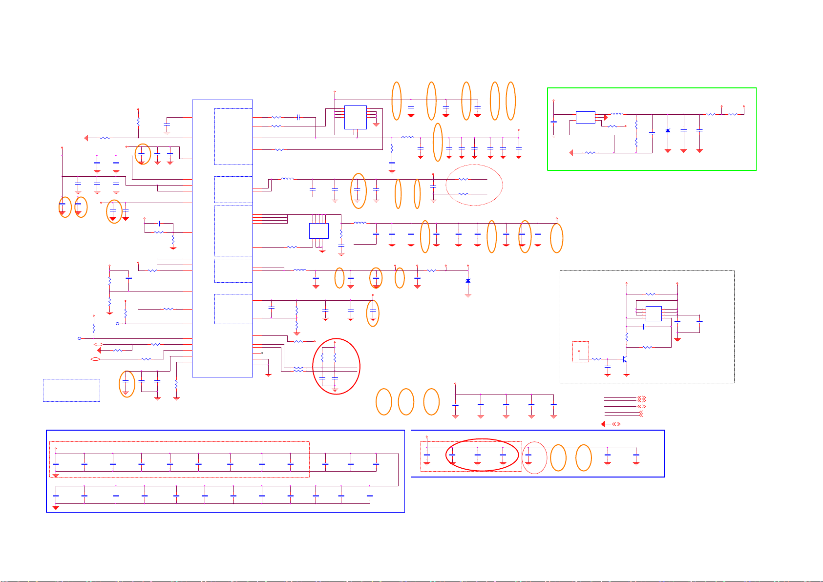
9.4 B 715G9907SSB
9-4-1POWER
2K19 MT5806 platform
R4115
VIN < 5.5V to trigger mute=Low.
C4128
10uF 16V
C4102
NC/100NF 16V
3V3SB
MOVE
3V3SB
MUTE_CTL
PWRDN
LO = > MUTE
HI = > UN-MUTE
HI = > UN-MUTE
LO = > MUTE
Bottom side of Ma in Chip
C4423
1uF 16V
MOVE
R4136
10K 5%
22K 1%
C4126
10uF 16V
C4129
10uF 16V
AVDD3V3
TP4100
R409
Main_12V
C4150
R4122
45.3K 1%
R4121
10K 1%
47K 1%
C4164
100NF 16V
C4101
100NF 16V
NC/10UF 10V
1.2 x ( 1+ 64 . 9 K/ 2 0K ) = 5 .0 9 V
3V3SB
MUTE_CTL
MOVE
C4515
1uF 16V
C4103
100NF 16V
CPU_GPU_P
C4151
MOVE
10,22
MUTE_CTL:
A_MUTE:
DDRV DE-CAP.
DDRV
+5V_STB
C4130
17
C4439
10uF 6.3V
NC/10UF 10V
TP4101
Main_12V
R4116
100K 1%
C4131
4.7UF 6. 3V
C4124
C4105
C4117
NC/10uF 16V
10uF 16V
100NF 16V
MOVE
+5V_STB
C4120 NC/100NF 16V
R4120 64.9K 1/10W
DDRV_FB
GND_FB
R4102
Buck3_ACFB
0R05 OHM
C4114
NC/100NF 16V
0.6 x (1+45.3K/10K) = 3.3V
R4100
OPWRSB_PWR
R4135
10K 5%
Hi : No rmal
Lo : Standby
0R05 OHM
R4104 0R05 OHM
R4106
NC/0R05 OH M
C4154
C4152
NC/10UF 10% 10V
10uF 25V
10uF 16V
C4512
C4513
1uF 16V
1uF 16V
R4119
20K 1%
R4105
30.9K 1/10W
33
32
29
9
23
24
8
40
30
13
14
15
3
36
37
12
2
1
35
31
U701
VCC
VDET
VIN1
VIN2
VIN3
VIN3
VIN4
VIN_LDO
FB1
VSEN2
RGND2
VSEN3
FB4
EN_CTRL
SOC_REST
VIN1_OK
MUTE_IN
MUTE_OUT#
VCAP
ENTRIP
RT5090CGQW
C4514
1uF 16V
DDRV_VPP
MOVE
8
7
6
5
C4147
22uF 6.3V
C4163
NC/1uF 2 5V
MOV E
C4159
NC/22uf 20% 6.3V
C4161
NC/4.7U F 10% 10V
MOVE
C4438
100NF 16V
MO V E
MO V E
DVDD3V3
L4100
3.3UH
R4131
1R 1/10W 5%
C4113
3.3NF 50V
C4138
22uF 6.3V
MO V E
MO V E
C4122
10uF 16V
MOV E
C4118
10uF 16V
DDRV
C4108
100NF 16V
MO V E
C4139
C4141
22uF 6.3V
22uF 6.3V
MOVE
DVDD3V3_SOC
AVDD3V3
R4123
0R05 1/4W
C4111
100NF 16V
DDRV_VPP=2.5V
0.8 x (1+47K/22K) = 2.5V
MOVE
CPU_GPU_P
Bottom side of Main Chip
C4465
10uF 6.3V
MOV EMO V EMOV E MO V E
C4133
10uF 16V
Close to DRAM
0R05 OHM
0R05 OHM
C4142
22uF 6.3V
AVDD3V3_SOC
1 2
C4155
NC/10uF 16V
C4134
10uF 16V
DDRV_FB
GND_FB
C4143
22uF 6.3V
Updated on 2018/3/23
ZD4100
MM3Z3V6B-HAF
C4153
10uF 16V
C4132
10uF 16V
R4101
R4103
CPU_GPU_P
C4534
C4532
NS/22uF/10V
NS/1uF/10V
C4448
C4454
10uF 6.3V
10uF 6.3V
0622 Modify to 0603 size
C4125
C4123
NC/10UF 10% 10V
NC/10UF 10% 10V
DDRV=1.2V
C4148
AVDD3V3=3.3V
C4535
NS/22uF/10V
C4453
10uF 6.3V
+5V_STB
NC/22uf 20% 6.3V
C4107
100NF 16V
C4109
NC/100NF 16V
8/27 to 04 0 2
C4533
NS/22uF/10V
C4466
1uF 16V
+5V_STB
4
5
C724
10uF 25V
Updated on 2018/3/26
CPU & GPU=1.0V
CPU_GPU_P
C4110
100NF 16V
MOV EMO V EMOV E
C4536
NS/22uF/10V
MOVE
U707
SY8089AAAC
LX3IN
2
GND
1
EN
FB
2A
R2
R742
18K OHM 1%
+5V_STB TO +5V_SW BY VCCK
VCCK
R740
1K 5%
MOVE
L704
2.2uH
R748
+5V_STB
4K7 5%
C701
100NF 16V
STB_SCL
STB_SDA
PMIC_INT
OPWRSB
OPWRSB_PWR
GND
C4472
100NF 16V
2.95 A
R746
75K 1%
R751
6.2K 1%
R781
Q706 AON4421
8
D
7
D
6
D
5
OPWRSB
OPWRSB_PWR
C711
33PF 50V
NC/0R05
STB_SCL
STB_SDA
PMIC_INT
ZD706
1 2
1
D
2
D
3
D
G4S
5,6
5,18,22
R1
C716 1UF 5 0V
R733
33K 1/10W 5%
R738 22K 1/10W
Q707
BC847N3
5,6,7,8,9,1 0,11,12,13,14,15, 16,17,18,19,20,21, 22
C4473
100NF 16V
3V3SB
R750
0 OHM 1/8W
C729
C725
BZT52-B3V6
10uF 16V
NC/10UF 10V
3V3SB_SOC
R701
0 OHM 1/8W
+5V_SW+5V_STB
MAX=2.0A
C786
C785
10uF 16V
10uF 16V
6
6
17
Main_12V
RT5090
28
BOOT1
27
UGATE1
Buck1
10A
Buck2
3A
Buck3
4A
Buck4
3A
LDO
300mA
C4516
1uF 16V
PHASE1
LGATE1
VLDO
FB_LDO
PGND
AGND
26
25
10
LX2
11
LX2
18
LX3
19
LX3
20
LX3
21
LX3
17
LG3
6
LX4
7
LX4
5
4
16
PMIC_INT
INT#
38
SCL
39
SDA
22
NC
41
34
C4522
1uF 16V
R4130
0R05 OHM
R4139
0R05 OHM
R4140
0R05 OHM
L4103
DDRV_FB
C4119
NC/100NF 16V
0.68uH 20% 4.5 A
AON7406
R4126
0R05 OHM
L4101
1uH
R4117
R4118
100R 5%
100R 5%
Q701
C4478
1uF 16V
C4104
100NF 16V
R4113
47K 1%
R4114
22K 1%
R4366
10K 1/10W
C4162
D5D6D7D8D
4
NC/10UF 10V
3V3SB
NC/1uF 25V
C4172
9
S1S2S3G
C166
100NF 16V
C4160
4.7UF 6. 3V
3V3SB
R729
3K3 5%
100pF 50V
C4387
MOVE
C167
1
G1
2
D1
3
D1
D14S2
C4135
22uF 6.3V
R4132
NC/0R05 OHM
C4121
NC/100NF 16V
R730
3K3 5%
STB_SCL
STB_SDA
100pF 50V
Add 0 710
U702
AON7934
10
100NF 16V
G2
S2
S2
S1/D29D1
C4136
NC/22uf 20% 6.3V
L4102 0.47uH
Buck3_ACFB
C4145
22uF 6.3V
C4112
100NF 16V
C4381
C4349
100NF 16V
C4342
100NF 16V
C4519
1UF 50V
C4511
100NF 16V
C4523
100NF 16V
C4521
100NF 16V
C4373
100NF 16V
C4351
100NF 16V
C4357
100NF 16V
C4352
100NF 16V
100NF 16V
C4390
100NF 16V
C4391

9-4-2 System Power
BL_ON/POK
AU_12V
Main_12V
MAI N PO WER
16
14
12
10
8
6
4
2
STB_PWR
R703 NC/ 0R05
+5V_STB
Main_12V
R784 0R05
OPWRSB_PWR
R760
100R 5%
MP87 71 : M ax :1 0 A
Vin 4.5 V~ 17V
Vout = 0. 6 V ( 1+ ( R 1/ R 2
⊙
⊙
Vout = 0. 6 V ( 1+ ( 2 0/ 3 0
))
))=1.0V
DVDD3V3
C743
C752
100NF 16V
10uF 25V
R723
3K3 5%
C730
NC/100N 16V
CPU & G PU Ca pa c i to r s
CPU_GPU_P
Bott om si d e of M ai n C h ip
C4456
10uF 6.3V
C4441
1uF 16V
CN701
CONN
Big plane
C745
10uF 16V
C747
U709
G5725ADJT11U
4
VIN
1
EN
2
15
13
11
9
7
5
3
1
10uF 16V
NC/100NF 25V
LX
VFB
GND
C4431
1uF 16V
C746
3
5
R713
100K 5%
C748
1uF 16V
BL_DIG_DI M
OPWRSB_PWR
ZD707
ZD708
C707 100NF 16V
C708 100NF 16V
C709 NC/ 100NF 16V
U706
8
VIN
MP8771GQ
C703
100NF 16V
3
EN
7
PG
14
VCC
9
L711 2.2uH
R727
NC/100OH M
C714
NC/10N F 50V
R776
24K 1%
Vout = 0 .6 x (1+ 2 4000/ 24000 )= 1 .2V
C4450
1uF 16V
NC/BZ T52-B22
NC/BZ T52-B22
12
12
AU_12V
Main_12V
PGND311PGND412PGND210PGND513PGND1
C717
NC/22P 50V
C4432
100NF 16V
BST
SW
NC1
NC2
FB
SS
AGND
5
C4455
1uF 16V
Mod ify by E MI
2
16
1
15
4
6
Max : 8 00 m A
R743
0R05 1/10W
R725
1K OHM 1%
C702
22NF25V
ZD711
R777
24K 1%
1 2
R734
300R 1/10W 1%
C4469
1uF 16V
C4479
10uF 6.3V
NC/MMSZ4678
C749
0.1uF 50V
R2
OPWRSB_PWR
R708
20K 1%
R710
30K OHM 1%
C751
10uF 6.3V
C4470
1uF 16V
C4480
22UF 6. 3V
L703
0.33uH 20%
AVDD1V2
10uF 6.3V
C704
1UF 50V
C750
1NF 16V
R1
C744
3V3SB
R709
15K 5%
Q710
BC847N3
PGO O D
Norm al:open drain by pull-up vlotage timing
Abnormal :low
R700
3K OHM 1%
R741
10R 1%
DVDD3V3
R767
4K7 5%
ZD712
1 2
OPW RSB:
Normal: Low
Stand_by: Hi
OPWRSB
R715
47K 5%
Big plane
NC/MMSZ4678
22UF 6.3 V
R737
0R05 1/16W
R724 10K 1/8W
+5V_SW
DVDD3V3
C712
10uF 6.3V
Bott om si d e of Ma i n C hi p
VCCK
C4428
22uF 6.3V
0926 mo d if ied
1018 to 0 8 05
VCCK C a pa c it or s
C757
C731
100NF 16V
C4424
22uF 6.3V
C758
22UF 6. 3V
R764
10K 1/8W
BL_DIG_DI M
C759
22UF 6. 3V
U704
G9661-25ADJF11U
1
POK
2
VEN
3
VIN
VPP4NC
C718
1uF 16V
2.0A (S p ec . )
C4444
1uF 16V
DVDD3V3 DVD D3V3
R712
R711
100R
Q703
BC847N3
VCCK
C760
22UF 6.3 V
9
E-Pad
8
GND
7
ADJ
6
VO
5
R1
R2
R735
1.65K 1%
C4452
1uF 16V
C4550
C4467
100NF 16V
10uF 10V
R706
10K 5%
NC/0R 05 1/16W
R714
4K7 5%
BRIG HT_AD J:
Normal: Max:+3V3 , Min:0 V
Stand _By:0V
+5V_STB
eMM C 1 V8
(1A/ 60m il)
R728
2K 1%
1 2
R766
100R 1%
0.8 x ( 1+ 2 . 1K/1. 65K) = 1 . 8V
C4430
1uF 16V
0926 mo dif ied
ZD710
C4397
10uF 10V
R705
4K7 5%
R722
NC/BZT52H-C2V7
C4429
1uF 16V
0R05 1/10W
R779
0R05
R726
0R05
C715
10uF 6.3V
A_DIM_ADJ
ANALO G POW ER A VD D1V05_ STB
10uF 25V
R762
3K3 5%
DVDD1V8_EMMC
C4468
10uF 6.3V
1018 mo dif ied
C4411
1uF 16V
C797
BL_O N/O FF:
Inverte r on:High
Inverte r off: Low
C798
100NF 16V
R761
NC/100K1/16W
C792
3V3SB DVDD3V3
R768
NC/4. 7K1/16W
R765
INV_EN
0R05 1/16W
R770
NC/4. 7K1/16W
R763
10K 5%
Add/ 2 01609 13
U710 G5725ADJT11U
4
1
3
VIN
LX
5
EN
VFB
GND
2
NC/100N 16V
A_DIM_ADJ
OPWRSB
OPWRSB_PWR
INV_EN
GND
Op t ion b y USB F/ W U pgrad e
USB_PORT1_5V Main_12V
R769
NC/4. 7K1/16W
R771
100R
Q711
NC/BC847N3
C796
NC/10uF 6.3V
TYP = 3 00 m A
L710 2.2uH
R775
NC/100OH M
C794
NC/22P 50V
C793
NC/10N F 50V
R773
2K 1%
Vout = 0.6 x (1 + 20000 / 2600 0 )= 1 . 06 V
A_DIM_ADJ
OPWRSB
OPWRSB_PWR
INV_EN 17
R704
24K 1%
17
6
4,18,22
4,6,7,8, 9,10,11,12,13,14, 15,16,17,18,19,20, 21,22
R191
R192
NC/510OHM +-5% 1/4W
NC/510 OHM 5% 1/4W
R190
NC/510 OHM 5% 1/4W
R702
ZD705
20K 1%
1 2
3A/ 6 0 V
D703
1 2
SX36
BL_ON/POK
C790
NC/MMSZ4678
AVDD105_STB
R707
0R05
C799
NC/10UF 10V
10uF 6.3V

9-4-3 Peripheral
OSCL0
OSDA1
OSCL1
XTALI
XTALO
AVDD105_PDW_ STB
AVDD33_PDW_S TB
AVDD33_RGB_STB
VCCQ_EMMC
C4481
10uF 10V
EMMC_CLK EMMC_CLK#
EMMC_CMD
PDD0
PDD1
PDD2
PDD3
PDD4
PDD5
PDD6
PDD7
EMMC_RSTB
Core Pow e r
VCCK
C4392
22UF 6. 3V
VCCK
C4402
10uF 6.3V
AVSS33_RGB
AVDD33_PLL_STB
VCC3IO_EMMC
POR_OPT
C4464
ORESETB
1uF 16V
OPWRSB
RC6
R4317
0R05 1/16W
EMM C
R5036 0R05 1/ 16W
R5139 0R05 1/ 16W
R5140 0R05 1/ 16W
R5040 0R05 1/ 16W
R5041 0R05 1/ 16W
R5042 0R05 1/ 16W
R5043 0R05 1/ 16W
R5044 0R05 1/ 16W
R5045 0R05 1/ 16W
VCC3IO_EMMC
R5031
0R05 1/16W
C4528
10uF 6.3V
Close to M ain C h ip
C4407
22UF 6. 3V
R4030
4K7 5%
EMMC_RST#
C4033
100NF 16V
AL5
AM5
AK8
AJ8
AN29
AP29
AN21
AD24
AH24
AC25
AK22
AP9
AM23
AL22
AM15
AH17
C4403
100NF 16V
C4405
100NF 16V
U401-7
OSDA0
OSCL0
OSDA1
OSCL1
XTALI
XTALO
AVDD105_PDW_STB
AVDD33_PDW_STB
AVDD33_RGB_STB
AVSS33_RGB
AVDD33_PLL_STB
DVDD33_EMMC
POR_OPT
ORESETB
OPWRSB
OIRI
MT5806IFEQ
EMMC_CMD_R
C4035 1uF 16V
VCC3IO_EMMC
VCC_EMMC
TP4430
TP4431
TP4432
Chang e to 060 3 size
C4529
22uF 6.3V
C4406
100NF 16V
AK15
U0TX
AJ15
U0RX
AL8
U1TX
AM8
U1RX
AL13
EMMC_D0
AL14
EMMC_D1
AP14
EMMC_D2
AP12
EMMC_D3
AM12
EMMC_D4
AM13
EMMC_D5
AN14
EMMC_D6
AM14
EMMC_D7
EMMC_DS
SF_CE
SF_CLK
SF_IN
SF_OUT
FSRC_W R
STB_SCL
STB_SDA
AN12
AP10
AM11
AN10
AJ10
AJ9
AH10
AK10
W30
AH14
AJ14
EMMC_CMD
EMMC_CLK
EMMC_RST
VCC3IO_EMMC
R4041 NC/10K 1/ 16W 5%
R4034 NC/10K 1/ 16W 5%
R4038 NC/10K 1/ 16W 5%
R4037 NC/10K 1/ 16W 5%
R4039 NC/10K 1/ 16W 5%
R4033 NC/10K 1/ 16W 5%
R4036 NC/10K 1/ 16W 5%
R4035 NC/10K 1/ 16W 5%
R4040 NC/10K 1/ 16W 5%
U408
THGBMNG5D1LBAIT
A3
DAT0
A4
DAT1
A5
DAT2
A6
VSS
A7
NC
B2
DAT3
B3
DAT4
B4
DAT5
B5
DAT6
B6
DAT7
C2
VDDI
C4
Vssq
C5
NC
C6
Vccq
D4
A1 index
E5
NC
E6
Vcc
E7
Vss
E8
NC
E9
NC
E10
NC
F5
Vcc
F10
NC
G3
NC
NCB1NCC1NC
C4537
22uF 6.3V
C4404
100NF 16V
C4408
100NF 16V
STB_SCL
STB_SDA
N1
U0TXOSDA0
U0RX
U1TX
U1RX
PDD0PDD0
PDD1
PDD2
PDD3
PDD4
PDD5
PDD6
PDD7
EMMC_CMD
EMMC_CLK
EMMC_RSTB
EMMC_DS
FSRC_W R
NC
NC
Vssq
Vccq
Vssq
Vccq
Vssq
Vccq
Vssq
CLK
CMD
Vccq
NC
Vcc
Vss
NC
NC
RSTN
Vcc
VSS
Vss
DS
NC
Vss
TP401
TP402
TP441
VCC3IO_EMMC
P10
P7
P6
P5
P4
P3
N5
N4
N2
M6
M5
M4
K10
K9
K8
K7
K6
K5
EMMC_RST#
J10
J5
H10
H5
DS
G10
G5
C4427
100NF 16V
R8081
4K7 5%
EMMC_CLK#
EMMC_CMD_R
VCC_EMMC
C4203
4.7PF 50V
EMMC_DS
R518
0R05 1/16W
24M Hz CR Y S T AL
XTALI
DVDD3V3
DVDD3V3
R4031
NC/10K 1/16W 5%
Reset Ci r cu i t
close to ma i n c h ip fo r E S D
ORESETB
UART Po rt 0
U0TX
U0RX
FOR COD E DOW NLO AD AN D DEBUG
EMM C VC C / VCCQ Pow er
NC/0R 05 1/10W
C4005
12pF 50V
R4027
VCC_EMMC
VCCQ_EMMC
R4006
1K 5%
R401
4K7 5%
1
VCC_EMMC
C4400
100NF 16V
C4459
100NF 16V
C4399
10uF 6.3V
C4458
100NF 16V
2 4
24MHz
R4028
0R05 1/10W
C4140
10NF 50V
3V3SB
R402
4K7 5%
R405 100R 5%
R410 100R 5%
X401
3
DVDD1V8_EMMC
C4461
10uF 6.3V
C4401
100NF 16V
C4460
10uF 6.3V
C4457
100NF 16V
XTALO
C4006
12pF 50V
1.8 V
VCC3IO_EMMC
12
ZD4108
NC/AZ5123-01H
1
2
3
VCC3IO_EMMC
VCC_EMMC
C4462
10uF 6.3V
C4398
100NF 16V
C4463
10uF 6.3V
3V3SB
R4013
27K 1%
R4014
20K 1%
3V3SB
D401
BAV99
STB_SCL
STB_SDA
5
OPWRSB
1
2
D402
BAV99
CN403
3
CONN
1
2
3
SYSTE M EEP ROM
SYS_EEPROM_WP
OSCL0
OSDA0
SYS_E EPRO M _W P
Low: write
High: Write protection
STRAPP ING
LED_PWM0
LED_PWM1
LED_PWM2
Anal o g Pow er
3V3SB_SOC AVDD105_STB
POR
17
11
11
10
10
17
16,17
16,17
16,22
14,22
14,22
R4029
R4018
10K 5%
R4019
10K 5%
R4017
10K 5%
AVDD33_PDW_S TB
AVDD33_RGB_STB
AVDD33_PLL_STB
POR_OPT
SYS_EEPROM_WP
OSCL0
OSDA0
OSCL1
OSDA1
LED_PWM1
LED_PWM0
LED_PWM2
RC6
U0TX
U0RX
NC/0R 05 1/16W
C4510
100NF 16V
R443
NC/4K7 1/16W 5%
R472
0R05 1/16W
GND
DVDD3V3
R4023
NC/4K7 5%
C4412
100NF 16V
R4025
C5090
100NF 16V
3V3SB
R443: NA
R472: Mount
4
STB_SCL
4
STB_SDA
OPWRSB
SYS_EEPROM_WP
OSCL0
OSDA0
OSCL1
OSDA1
LED_PWM1
LED_PWM0
LED_PWM2
RC6
U0TX
U0RX
4,5,7,8, 9,10,11,12,13,14, 15,16,17,18,19,20, 21,22
DVDD3V3
R4026
NC/1K2 OHM
NC/1K2 OHM
C5091
NC/100pF 50V
NC/100pF 50V
C4020
NC/220nF 16V
U409
VCC
WC
SCL
1
E0
2
E1
3
E2
VSS4SDA
8
7
6
5
NC/M24128-BRMN6TP
I2C A D DR E SS "A 0 "
AVDD105_PDW_STB
C4414
C4413
Exter n al Re s etInter n al PO R
R443: Mo u nt
R472: NC
100NF 16V

9-4-4 DRR4*2
EMI0_A0
EMI0_A1
EMI0_A2
EMI0_A3
EMI0_A4
EMI0_A5
EMI0_A6
EMI0_A7
EMI0_A8
EMI0_A9
EMI0_A10
EMI0_A11
EMI0_A12
EMI0_A13
EMI0_BA0
EMI0_BA1
EMI0_CS0_N
EMI0_CLK_T
EMI0_CLK_C
EMI0_CKE0
EMI0_BG0
EMI0_RAS_N
EMI0_CAS_N
EMI0_WE_N
EMI0_ODT
EMI0_RESET_N
EMI0_ACT_N
EMI1_A0
EMI1_A1
EMI1_A2
EMI1_A3
EMI1_A4
EMI1_A5
EMI1_A6
EMI1_A7
EMI1_A8
EMI1_A9
EMI1_A10
EMI1_A11
EMI1_A12
EMI1_A13
EMI1_BA0
EMI1_BA1
EMI1_CS0_N
EMI1_CLK_T
EMI1_CLK_C
EMI1_CKE0
EMI1_BG0
EMI1_RAS_N
EMI1_CAS_N
EMI1_WE_N
EMI1_ODT
EMI1_RESET_N
EMI1_ACT_N
DDRV
DDRV_A_CA
DDRV_A_DQ
DDRV_A_CK
DDRV_B_CA
DDRV_B_DQ
DDRV_B_CK
DRAM# 1 B y pa s s Ca p
DDRV
C4359
10uF 6.3V
C4363
100NF 16V
Botto m s i de o f D R AM # 1
DDRV
DRAM# 2 B y pa s s C ap
C4388
10uF 6.3V
C4343
100NF 16V
Botto m s i de o f D R AM # 2
AA12
K9
W9
W6
U8
N7
T9
J8
V8
W7
V5
N4
W8
R8
V6
N8
P8
P6
N6
N5
M8
K8
T7
V9
L8
M5
K7
M4
B6
G8
G1
F7
E8
G6
A7
G5
H3
J3
D6
H1
E6
J4
E9
E7
D3
D4
D5
F9
A6
E5
H6
G9
D7
B7
C7
U12
V12
Y12
W12
M12
N12
R12
T12
P12
U401-1
EMI0_A0
EMI0_A1
EMI0_A2
EMI0_A3
EMI0_A4
EMI0_A5
EMI0_A6
EMI0_A7
EMI0_A8
EMI0_A9
EMI0_A10
EMI0_A11
EMI0_A12
EMI0_A13
EMI0_BA0
EMI0_BA1
EMI0_CS0_N
EMI0_CLK_T
EMI0_CLK_C
EMI0_CKE0
EMI0_BG0
EMI0_RAS_N
EMI0_CAS_N
EMI0_WE_N
EMI0_ODT
EMI0_RESET_N
EMI0_ACT_N
EMI1_A0
EMI1_A1
EMI1_A2
EMI1_A3
EMI1_A4
EMI1_A5
EMI1_A6
EMI1_A7
EMI1_A8
EMI1_A9
EMI1_A10
EMI1_A11
EMI1_A12
EMI1_A13
EMI1_BA0
EMI1_BA1
EMI1_CS0_N
EMI1_CLK_T
EMI1_CLK_C
EMI1_CKE0
EMI1_BG0
EMI1_RAS_N
EMI1_CAS_N
EMI1_WE_N
EMI1_ODT
EMI1_RESET_N
EMI1_ACT_N
DDRV_A_CA
DDRV_A_CA
DDRV_A_DQ
DDRV_A_DQ
DDRV_A_CK
DDRV_B_CA
DDRV_B_CA
DDRV_B_DQ
DDRV_B_DQ
DDRV_B_CK
MT5806IFEQ
C4341
100NF 16V
C4364
100NF 16V
C4356
100NF 16V
C4361
100NF 16V
EMI0_DQS0_T
EMI0_DQS0_C
EMI0_DQS1_T
EMI0_DQS1_C
EMI1_DQS0_T
EMI1_DQS0_C
EMI1_DQS1_T
EMI1_DQS1_C
AVDD33_RDD R
AVDD10_RDD R
AVDD10_RDD R
AVDD10_RDD R
AVDD10_RDD R
C4347
100NF 16V
C4340
100NF 16V
C4389
100NF 16V
C4345
100NF 16V
EMI0_DQM0
EMI0_DQ0
EMI0_DQ1
EMI0_DQ2
EMI0_DQ3
EMI0_DQ4
EMI0_DQ5
EMI0_DQ6
EMI0_DQ7
EMI0_DQM1
EMI0_DQ8
EMI0_DQ9
EMI0_DQ10
EMI0_DQ11
EMI0_DQ12
EMI0_DQ13
EMI0_DQ14
EMI0_DQ15
CHA
EMI1_DQM0
EMI1_DQ0
EMI1_DQ1
EMI1_DQ2
EMI1_DQ3
EMI1_DQ4
EMI1_DQ5
EMI1_DQ6
EMI1_DQ7
EMI1_DQM1
EMI1_DQ8
EMI1_DQ9
EMI1_DQ10
EMI1_DQ11
EMI1_DQ12
EMI1_DQ13
EMI1_DQ14
EMI1_DQ15
CHB
EMI_TP
EMI_TN
EMI_EXTR
R3
M2
M1
K3
P1
J1
P3
J2
P2
H2
N2
K2
R2
R1
M3
T1
L1
T2
L2
U3
L3
U2
E3
B1
B2
A4
D2
B5
C1
C5
C2
C6
C3
B4
E1
E2
C4
F3
A2
F2
B3
G3
A3
G2
K10
K11
A8
M13
M19
T13
Y13
J9
C4368
100NF 16V
C4339
100NF 16V
C4344
100NF 16V
C4436
100NF 16V
EMI0_DQM0
EMI0_DQS0_T
EMI0_DQS0_C
EMI0_DQ0
EMI0_DQ1
EMI0_DQ2
EMI0_DQ3
EMI0_DQ4
EMI0_DQ5
EMI0_DQ6
EMI0_DQ7
EMI0_DQM1
EMI0_DQS1_T
EMI0_DQS1_C
EMI0_DQ8
EMI0_DQ9
EMI0_DQ10
EMI0_DQ11
EMI0_DQ12
EMI0_DQ13
EMI0_DQ14
EMI0_DQ15
EMI1_DQM0
EMI1_DQS0_T
EMI1_DQS0_C
EMI1_DQ0
EMI1_DQ1
EMI1_DQ2
EMI1_DQ3
EMI1_DQ4
EMI1_DQ5
EMI1_DQ6
EMI1_DQ7
EMI1_DQM1
EMI1_DQS1_T
EMI1_DQS1_C
EMI1_DQ8
EMI1_DQ9
EMI1_DQ10
EMI1_DQ11
EMI1_DQ12
EMI1_DQ13
EMI1_DQ14
EMI1_DQ15
EMI_TP
EMI_TN
AVDD33_RDD R
AVDD10_RDD R
EMI_EXTR
C4346
100NF 16V
C4371
100NF 16V
C4369
100NF 16V
C4386
100NF 16V
MTP47
MTP48
MTP49
MTP50
MTP51
MTP52
MTP53
MTP54
C4362
100NF 16V
C4360
100NF 16V
C4372
100NF 16V
065G 04021 0 412K F
DDR_VTT
RP401 120R
1
2
3
4
RP402 120R
1
2
3
4
RP403 120R
1
2
3
4
RP404 120R
1
2
3
4
R4342
R4343
R4344
R4345
R4346
R4347
VCCK
C4338
100NF 16V
C4348
100NF 16V
120R 1%
120R 1%
120R 1%
120R 1%
120R 1%
120R 1%
8
EMI0_A3
7
EMI0_A9
6
EMI0_A7
5
EMI0_A13
8
EMI0_A0
7
EMI0_A11
6
EMI0_A8
5
EMI0_A2
8
EMI0_A1
7
EMI0_A12
6
EMI0_BA1
5
EMI0_A10
8
7
EMI0_ACT_N
6
EMI0_A4
5
EMI0_BA0
EMI0_A5
EMI0_CAS_N
EMI0_RAS_N
EMI0_WE_N
EMI0_BG0
EMI0_A6
AVDD10_RDD R
AVDD10_RDD R
AVDD10_RDD R
AVDD10_RDD R
C4354
100NF 16V
DDR_VTT
C4365
100NF 16V
C4367
100NF 16V
R4336
R4337
R4338
R4348
R4349
R4350
RP405 120R
1
2
3
4
RP416 120R
1
2
3
4
RP406 120R
1
2
3
4
RP407 120R
1
2
3
4
120R 1%
120R 1%
120R 1%
120R 1%
120R 1%
120R 1%
8
7
6
5
8
7
6
5
8
7
6
5
8
7
6
5
C4366
100NF 16V
C4370
100NF 16V
EMI1_A5
EMI1_A9
EMI1_A7
EMI1_A13
EMI1_A0
EMI1_A8
EMI1_A11
EMI1_A2
EMI1_A12
EMI1_BA1
EMI1_A3
EMI1_A1
EMI1_A10
EMI1_ACT_N
EMI1_BA0
EMI1_RAS_N
EMI1_CAS_N
EMI1_A4
EMI1_WE_N
EMI1_BG0
EMI1_A6
NEAR M ai n C h ip
Diff er e nt ia l C l oc k
DDRV_VPP
MTP23
EMI0_CLK_T
EMI0_CLK_C
EMI1_CLK_T
EMI1_CLK_C
C4319
100NF 16V
MTP1
MTP2
MTP3
MTP4
MTP5
MTP6
MTP7
MTP8
MTP9
MTP10
MTP11
MTP12
MTP13
MTP14
MTP15
MTP16
MTP17
MTP18
MTP19
MTP20
MTP21
MTP22
C4316
100NF 16V
EMI0_RESET_N
C4333
NS/0.1uF /16V/X7R
C4303
100NF 16V
EMI0_DQ0
EMI0_DQ1
EMI0_DQ2
EMI0_DQ3
EMI0_DQ4
EMI0_DQ5
EMI0_DQ6
EMI0_DQ7
EMI0_DQ8
EMI0_DQ9
EMI0_DQ10
EMI0_DQ11
EMI0_DQ12
EMI0_DQ13
EMI0_DQ14
EMI0_DQ15
EMI0_DQS1_T
EMI0_DQS1_C
EMI0_DQS0_T
EMI0_DQS0_C
EMI0_DQM1
EMI0_DQM0
EMI0_RESET_N
DDRV_VPP
R4320
240 OHM 1%
DDRV
DVDD3V3_SOC
NEAR DR A M
EMI0_CLK_T
R4301
NS/82
EMI0_CLK_C
NEAR DR A MNEAR M ai n C h ip
EMI1_CLK_T
R4302
NS/82
EMI1_CLK_C
C4305
100NF 16V
U402
G2
DQL0
F7
DQL1
H3
DQL2
H7
DQL3
H2
DQL4
H8
DQL5
J3
DQL6
J7
DQL7
A3
DQU0
B8
DQU1
C3
DQU2
C7
DQU3
C2
DQU4
C8
DQU5
D3
DQU6
D7
DQU7
B7
DQSU
A7
DQSU_n
G3
DQSL
F3
DQSL_n
E2
DMU_b/DBIU _n
E7
DML_b/DBIL_n
M1
VREFAC
P1
RESER#
F9
ZQ
B1
VPP
R9
VPP
A1
VDDQ
A9
VDDQ
C1
VDDQ
D9
VDDQ
F2
VDDQ
F8
VDDQ
G1
VDDQ
G9
VDDQ
J2
VDDQ
J8
VDDQ
B3
VDD
B9
VDD
D1
VDD
G7
VDD
J1
VDD
J9
VDD
L1
VDD
L9
VDD
R1
VDD
T9
VDD
K4A4G165WE-BCTD
R4316
0R05 1/16W
DDR4# 1
DDR4 X1 6 (F P GA 9 6)
C4326
100NF 16V
P3
EMI0_A0
A0
P7
EMI0_A1
A1
R3
EMI0_A2
A2
N7
EMI0_A3
A3
N3
EMI0_A4
A4
P8
EMI0_A5
A5
P2
EMI0_A6
A6
R8
EMI0_A7
A7
R2
EMI0_A8
A8
R7
EMI0_A9
A9
M3
ACT_n
CK_n
CS_n
VSSQ
VSSQ
VSSQ
VSSQ
VSSQ
VSSQ
VSSQ
VSSQ
VSSQ
VSSQ
EMI0_A10
T2
EMI0_A11
A11
M7
EMI0_A12
T8
EMI0_A13
A13
T7
NC
T3
R4327 1K 5%
PAR
N9
R4326 1K 5%
TEN
L3
EMI0_ACT_N
P9
R4325
N2
EMI0_BA0
BA0
N8
EMI0_BA1
BA1
M2
EMI0_BG0
BG0
K7
EMI0_CLK_T
CK
K8
EMI0_CLK_C
L7
EMI0_CS0_N
M8
EMI0_CAS_N
K3
EMI0_ODT
ODT
L8
EMI0_RAS_N
L2
EMI0_WE_N
K2
EMI0_CKE0
CKE
A2
A8
C9
D2
D8
E3
E8
F1
H1
H9
B2
VSS
E1
VSS
E9
VSS
G8
VSS
K1
VSS
K9
VSS
M9
VSS
N1
VSS
T1
VSS
10K 5%
DDRV
MTP46
A10/AP
A12/BC_n
ALERT_n
CAS_n/A15
RAS_n/A16
WE_n/A14
AVDD33_RDD R
AVDD33_RDD R
C4445
1uF 16V
R4305
1K OHM 1%
C4308
100NF 16V
A_VREFCA B_VREFCA2
R4307
1K OHM 1%
C4315
100NF 16V
MTP24
MTP25
MTP26
MTP27
MTP28
MTP29
MTP30
MTP31
MTP32
MTP33
MTP34
MTP35
MTP36
MTP37
MTP38
MTP39
MTP40
MTP41
MTP43
MTP42
MTP44
MTP45
C4327
100NF 16V
EMI1_RESET_N
C4334
NS/0.1uF/ 16V/X7R
DDR4# 2 R e f V ol t .DDR4# 1 R ef Vo l t.Diff er e nt ia l C l oc k
GND
DDR4# 2
U403
G2
EMI1_DQ0
EMI1_DQ1
EMI1_DQ2
EMI1_DQ3
EMI1_DQ4
EMI1_DQ5
EMI1_DQ6
EMI1_DQ7
EMI1_DQ8
EMI1_DQ9
EMI1_DQ10
EMI1_DQ11
EMI1_DQ12
EMI1_DQ13
EMI1_DQ14
EMI1_DQ15
EMI1_DQS1_T
EMI1_DQS1_C
EMI1_DQS0_T
EMI1_DQS0_C
EMI1_DQM1
EMI1_DQM0
B_VREFCA2A_VREFCA
EMI1_RESET_N
DDRV_VPP
R4321
240 OHM 1%
DDRV
F7
H3
H7
H2
H8
J3
J7
A3
B8
C3
C7
C2
C8
D3
D7
B7
A7
G3
F3
E2
E7
M1
P1
F9
B1
R9
A1
A9
C1
D9
F2
F8
G1
G9
J2
J8
B3
B9
D1
G7
J1
J9
L1
L9
R1
T9
DQL0
DQL1
DQL2
DQL3
DQL4
DQL5
DQL6
DQL7
DQU0
DQU1
DQU2
DQU3
DQU4
DQU5
DQU6
DQU7
DQSU
DQSU_n
DQSL
DQSL_n
DMU_b/DBIU _n
DML_b/DBIL_n
VREFAC
RESER#
ZQ
VPP
VPP
VDDQ
VDDQ
VDDQ
VDDQ
VDDQ
VDDQ
VDDQ
VDDQ
VDDQ
VDDQ
VDD
VDD
VDD
VDD
VDD
VDD
VDD
VDD
VDD
VDD
DDR4 X1 6 (F P GA 9 6)
K4A4G165WE-BCTD
EMI_EXTR
R4315
NS
R4318
NS/47_1%
DDRVDDRV
R4306
1K OHM 1%
R4308
1K OHM 1%
Near D R AMNear D RA M
C4304
100NF 16V
C4317
100NF 16V
4,5,6,8,9, 10,11,12,13,14,15, 16,17,18,19,20,21, 22
A10/AP
A12/BC_n
ACT_n
ALERT_n
CK_n
CS_n
CAS_n/A15
RAS_n/A16
WE_n/A14
VSSQ
VSSQ
VSSQ
VSSQ
VSSQ
VSSQ
VSSQ
VSSQ
VSSQ
VSSQ
R4319
47R 1%
A0
A1
A2
A3
A4
A5
A6
A7
A8
A9
A11
A13
NC
PAR
TEN
BA0
BA1
BG0
CK
ODT
CKE
VSS
VSS
VSS
VSS
VSS
VSS
VSS
VSS
VSS
EMI_TP
EMI_TN
P3
EMI1_A0
P7
EMI1_A1
R3
EMI1_A2
N7
EMI1_A3
N3
EMI1_A4
P8
EMI1_A5
P2
EMI1_A6
R8
EMI1_A7
R2
EMI1_A8
R7
EMI1_A9
M3
EMI1_A10
T2
EMI1_A11
M7
EMI1_A12
T8
EMI1_A13
T7
T3
R4324 1K 5%
N9
R4323 1K 5%
L3
EMI1_ACT_N
P9
R4322 10K 5%
N2
EMI1_BA0
N8
EMI1_BA1
M2
EMI1_BG0
K7
EMI1_CLK_T
K8
EMI1_CLK_C
L7
EMI1_CS0_N
M8
EMI1_CAS_N
K3
EMI1_ODT
L8
EMI1_RAS_N
L2
EMI1_WE_N
K2
EMI1_CKE0
A2
A8
C9
D2
D8
E3
E8
F1
H1
H9
B2
E1
E9
G8
K1
K9
M9
N1
T1
DDRV

9-4-5 DRR4*2-2
G20
EMI2_A0
H14
EMI2_A1
G11
EMI2_A2
G14
EMI2_A3
D17
EMI2_A4
G13
EMI2_A5
F20
EMI2_A6
G12
EMI2_A7
J11
EMI2_A8
E11
EMI2_A9
H18
EMI2_A10
J12
EMI2_A11
D15
EMI2_A12
D11
EMI2_A13
J17
EMI2_BA0
H15
EMI2_BA1
J15
EMI2_CS0_N
H17
EMI2_CLK_T
G17
EMI2_CLK_C
J18
EMI2_CKE0
D20
EMI2_BG0
F14
EMI2_RAS_N
F13
EMI2_CAS_N
J19
EMI2_WE_N
E17
EMI2_ODT
E19
EMI2_RESET_N
F18
EMI2_ACT_N
H25
EMI3_A0
G24
EMI3_A1
F22
EMI3_A2
E24
EMI3_A3
D26
EMI3_A4
H24
EMI3_A5
D28
EMI3_A6
J22
EMI3_A7
J21
EMI3_A8
G22
EMI3_A9
G27
EMI3_A10
H20
EMI3_A11
F25
EMI3_A12
H23
EMI3_A13
B27
EMI3_BA0
E25
EMI3_BA1
H26
EMI3_CS0_N
F27
EMI3_CLK_T
E27
EMI3_CLK_C
A27
EMI3_CKE0
D27
EMI3_BG0
F26
EMI3_RAS_N
J23
EMI3_CAS_N
C27
EMI3_WE_N
B26
EMI3_ODT
C28
EMI3_RESET_N
H27
EMI3_ACT_N
DDRV
DDRV_C_C A
DDRV_C_D Q
DDRV_C_C K
L16
L17
L13
L14
L15
U401-2
EMI2_A0
EMI2_A1
EMI2_A2
EMI2_A3
EMI2_A4
EMI2_A5
EMI2_A6
EMI2_A7
EMI2_A8
EMI2_A9
EMI2_A10
EMI2_A11
EMI2_A12
EMI2_A13
EMI2_BA0
EMI2_BA1
EMI2_CS0_N
EMI2_CLK_T
EMI2_CLK_C
EMI2_CKE0
EMI2_BG0
EMI2_RAS_N
EMI2_CAS_N
EMI2_WE_N
EMI2_ODT
EMI2_RESET_N
EMI2_ACT_N
EMI3_A0
EMI3_A1
EMI3_A2
EMI3_A3
EMI3_A4
EMI3_A5
EMI3_A6
EMI3_A7
EMI3_A8
EMI3_A9
EMI3_A10
EMI3_A11
EMI3_A12
EMI3_A13
EMI3_BA0
EMI3_BA1
EMI3_CS0_N
EMI3_CLK_T
EMI3_CLK_C
EMI3_CKE0
EMI3_BG0
EMI3_RAS_N
EMI3_CAS_N
EMI3_WE_N
EMI3_ODT
EMI3_RESET_N
EMI3_ACT_N
DDRV_C_C A
DDRV_C_C A
DDRV_C_D Q
DDRV_C_D Q
DDRV_C_C K
EMI2_DQM0
EMI2_DQS0_T
EMI2_DQS0_C
EMI2_DQ0
EMI2_DQ1
EMI2_DQ2
EMI2_DQ3
EMI2_DQ4
EMI2_DQ5
EMI2_DQ6
EMI2_DQ7
EMI2_DQM1
EMI2_DQS1_T
EMI2_DQS1_C
EMI2_DQ8
EMI2_DQ9
EMI2_DQ10
EMI2_DQ11
EMI2_DQ12
EMI2_DQ13
EMI2_DQ14
EMI2_DQ15
CHC
EMI3_DQM0
EMI3_DQS0_T
EMI3_DQS0_C
EMI3_DQ0
EMI3_DQ1
EMI3_DQ2
EMI3_DQ3
EMI3_DQ4
EMI3_DQ5
EMI3_DQ6
EMI3_DQ7
EMI3_DQM1
EMI3_DQS1_T
EMI3_DQS1_C
EMI3_DQ8
EMI3_DQ9
EMI3_DQ10
EMI3_DQ11
EMI3_DQ12
EMI3_DQ13
EMI3_DQ14
EMI3_DQ15
CHD
DDRV_D_C A
DDRV_D_C A
DDRV_D_D Q
DDRV_D_D Q
DDRV_D_C K
B11
B13
C13
B16
C11
B17
B12
C16
A12
A17
A13
D16
B10
C10
B14
A10
C14
D10
A15
B9
B15
C9
B20
C22
B22
C25
A20
B25
A21
A25
C21
C26
B21
A24
B19
C19
C23
D19
D24
B18
C24
A18
B24
C17
K20
L20
K18
L18
L19
EMI2_DQM0
EMI2_DQS0_T
EMI2_DQS0_C
EMI2_DQ0
EMI2_DQ1
EMI2_DQ2
EMI2_DQ3
EMI2_DQ4
EMI2_DQ5
EMI2_DQ6
EMI2_DQ7
EMI2_DQM1
EMI2_DQS1_T
EMI2_DQS1_C
EMI2_DQ8
EMI2_DQ9
EMI2_DQ10
EMI2_DQ11
EMI2_DQ12
EMI2_DQ13
EMI2_DQ14
EMI2_DQ15
EMI3_DQM0
EMI3_DQS0_T
EMI3_DQS0_C
EMI3_DQ0
EMI3_DQ1
EMI3_DQ2
EMI3_DQ3
EMI3_DQ4
EMI3_DQ5
EMI3_DQ6
EMI3_DQ7
EMI3_DQM1
EMI3_DQS1_T
EMI3_DQS1_C
EMI3_DQ8
EMI3_DQ9
EMI3_DQ10
EMI3_DQ11
EMI3_DQ12
EMI3_DQ13
EMI3_DQ14
EMI3_DQ15
DDRV_D_ CA
DDRV_D_ DQ
DDRV_D_ CK
DDRV
MTP101
MTP102
MTP103
MTP104
MTP105
MTP106
MTP107
MTP108
DDR_VTT DD R_VTT
RP408 120R
1
8
EMI2_A1
2
7
EMI2_A9
3
6
EMI2_A13
4
5
EMI2_A7
RP409 120R
1
8
EMI2_A0
2
7
EMI2_A11
3
6
EMI2_A8
4
5
EMI2_A2
RP410 120R
1
8
EMI2_BA1
2
7
EMI2_A3
3
6
EMI2_A12
4
5
EMI2_A10
RP411 120R
1
8
EMI2_ACT_N
2
7
EMI2_A4
3
6
EMI2_BA0
4
5
R4351
R4352
R4353
R4354
R4355
R4356
EMI2_A5 EMI3_RAS_N
EMI2_CAS_N
EMI2_RAS_N
EMI2_WE_N
EMI2_BG0
EMI2_A6
120R 1%
120R 1%
120R 1%
120R 1%
120R 1%
120R 1%
RP412 120R
1
2
3
4
RP413 120R
1
2
3
4
RP414 120R
1
2
3
4
RP415 120R
1
2
3
4
R4339
R4340
R4341
R4357
R4358
R4359
120R 1%
120R 1%
120R 1%
120R 1%
120R 1%
120R 1%
8
7
6
5
8
7
6
5
8
7
6
5
8
7
6
5
EMI3_A1
EMI3_A5
EMI3_A9
EMI3_A13
EMI3_A0
EMI3_A8
EMI3_A11
EMI3_A2
EMI3_A4
EMI3_A12
EMI3_BA1
EMI3_A3
EMI3_A10
EMI3_ACT_N
EMI3_BA0
EMI3_CAS_N
EMI3_A7
EMI3_WE_N
EMI3_BG0
EMI3_A6
MTP55
MTP56
MTP57
MTP58
MTP59
MTP60
MTP61
MTP62
MTP63
MTP64
MTP65
MTP66
MTP67
MTP68
MTP69
MTP70
MTP71
MTP72
MTP74
MTP73
MTP75
MTP99
MTP76
C4328
100NF 16V
EMI2_RESET_N
C4335
NS/0.1uF /16V/X7R
EMI2_DQ0
EMI2_DQ1
EMI2_DQ2
EMI2_DQ3
EMI2_DQ4
EMI2_DQ5
EMI2_DQ6
EMI2_DQ7
EMI2_DQ8
EMI2_DQ9
EMI2_DQ10
EMI2_DQ11
EMI2_DQ12
EMI2_DQ13
EMI2_DQ14
EMI2_DQ15
EMI2_DQS1_T
EMI2_DQS1_C
EMI2_DQS0_T
EMI2_DQS0_C
EMI2_DQM1
EMI2_DQM0
C_VREFCA
EMI2_RESET_N
R4328
240 OHM 1%
DDRV
DDRV_VPP
DDR4# 3 DDR4# 4
U404
G2
F7
H3
H7
H2
H8
J3
J7
A3
B8
C3
C7
C2
C8
D3
D7
B7
A7
G3
F3
E2
E7
M1
P1
F9
B1
R9
A1
A9
C1
D9
F2
F8
G1
G9
J2
J8
B3
B9
D1
G7
J1
J9
L1
L9
R1
T9
DQL0
DQL1
DQL2
DQL3
DQL4
DQL5
DQL6
DQL7
DQU0
DQU1
DQU2
DQU3
DQU4
DQU5
DQU6
DQU7
DQSU
DQSU_n
DQSL
DQSL_n
DMU_b/DBI U_n
DML_b/DBIL_n
VREFAC
RESER#
ZQ
VPP
VPP
VDDQ
VDDQ
VDDQ
VDDQ
VDDQ
VDDQ
VDDQ
VDDQ
VDDQ
VDDQ
VDD
VDD
VDD
VDD
VDD
VDD
VDD
VDD
VDD
VDD
DDR4 X1 6 (F P G A9 6)
A10/AP
A12/BC_n
ACT_n
ALERT_n
CK_n
CS_n
CAS_n/A15
RAS_n/A16
WE_n/A14
VSSQ
VSSQ
VSSQ
VSSQ
VSSQ
VSSQ
VSSQ
VSSQ
VSSQ
VSSQ
A0
A1
A2
A3
A4
A5
A6
A7
A8
A9
A11
A13
NC
PAR
TEN
BA0
BA1
BG0
CK
ODT
CKE
VSS
VSS
VSS
VSS
VSS
VSS
VSS
VSS
VSS
P3
EMI2_A0
P7
EMI2_A1
R3
EMI2_A2
N7
EMI2_A3
N3
EMI2_A4
P8
EMI2_A5
P2
EMI2_A6
R8
EMI2_A7
R2
EMI2_A8
R7
EMI2_A9
M3
EMI2_A10
T2
EMI2_A11
M7
EMI2_A12
T8
EMI2_A13
T7
T3
R4332 1K 5%
N9
R4331 1K 5%
L3
EMI2_ACT_N
P9
R4330 10K 5 %
N2
EMI2_BA0
N8
EMI2_BA1
M2
EMI2_BG0
K7
EMI2_CLK_T
K8
EMI2_CLK_C
L7
EMI2_CS0_N
M8
EMI2_CAS_N
K3
EMI2_ODT
L8
EMI2_RAS_N
L2
EMI2_WE_N
K2
EMI2_CKE0
A2
A8
C9
D2
D8
E3
E8
F1
H1
H9
B2
E1
E9
G8
K1
K9
M9
N1
T1
DDRV
MTP100
MTP77
MTP78
MTP79
MTP80
MTP81
MTP82
MTP83
MTP84
MTP85
MTP86
MTP87
MTP88
MTP89
MTP92
MTP90
MTP91
MTP93
MTP94
MTP95
MTP96
MTP98
MTP97
C4329
100NF 16V
EMI3_RESET_N
C4336
NS/0.1uF/ 16V/X7R
EMI3_DQ0
EMI3_DQ1
EMI3_DQ2
EMI3_DQ3
EMI3_DQ4
EMI3_DQ5
EMI3_DQ6
EMI3_DQ7
EMI3_DQ8
EMI3_DQ9
EMI3_DQ10
EMI3_DQ11
EMI3_DQ12
EMI3_DQ13
EMI3_DQ14
EMI3_DQ15
EMI3_DQS1_T
EMI3_DQS1_C
EMI3_DQS0_T
EMI3_DQS0_C
EMI3_DQM1
EMI3_DQM0
D_VREFCA
EMI3_RESET_N
R4329
240 OHM 1%
DDRV
K4A4G165WE-BCTD
DDRV_VPP
U405
G2
DQL0
F7
DQL1
H3
DQL2
H7
DQL3
H2
DQL4
H8
DQL5
J3
DQL6
J7
DQL7
A3
DQU0
B8
DQU1
C3
DQU2
C7
DQU3
C2
DQU4
C8
DQU5
D3
DQU6
D7
DQU7
B7
DQSU
A7
DQSU_n
G3
DQSL
F3
DQSL_n
E2
DMU_b/DBIU _n
E7
DML_b/DBIL_n
M1
VREFAC
P1
RESER#
F9
ZQ
B1
VPP
R9
VPP
A1
VDDQ
A9
VDDQ
C1
VDDQ
D9
VDDQ
F2
VDDQ
F8
VDDQ
G1
VDDQ
G9
VDDQ
J2
VDDQ
J8
VDDQ
B3
VDD
B9
VDD
D1
VDD
G7
VDD
J1
VDD
J9
VDD
L1
VDD
L9
VDD
R1
VDD
T9
VDD
K4A4G165WE-BCTD
P3
EMI3_A0
A0
P7
EMI3_A1
A1
R3
EMI3_A2
A2
N7
EMI3_A3
A3
N3
EMI3_A4
A4
P8
EMI3_A5
A5
P2
EMI3_A6
A6
R8
EMI3_A7
A7
R2
EMI3_A8
A8
R7
EMI3_A9
A9
M3
ACT_n
CK_n
CS_n
VSSQ
VSSQ
VSSQ
VSSQ
VSSQ
VSSQ
VSSQ
VSSQ
VSSQ
VSSQ
A11
A13
NC
PAR
TEN
BA0
BA1
BG0
ODT
CKE
VSS
VSS
VSS
VSS
VSS
VSS
VSS
VSS
VSS
CK
EMI3_A10
T2
EMI3_A11
M7
EMI3_A12
T8
EMI3_A13
T7
T3
R4335 1K 5%
N9
R4334 1K 5%
L3
EMI3_ACT_N
P9
R4333 10K 5%
N2
EMI3_BA0
N8
EMI3_BA1
M2
EMI3_BG0
K7
EMI3_CLK_T
K8
EMI3_CLK_C
L7
EMI3_CS0_N
M8
EMI3_CAS_N
K3
EMI3_ODT
L8
EMI3_RAS_N
L2
EMI3_WE_N
K2
EMI3_CKE0
A2
A8
C9
D2
D8
E3
E8
F1
H1
H9
B2
E1
E9
G8
K1
K9
M9
N1
T1
DDRV
A10/AP
A12/BC_n
ALERT_n
CAS_n/A15
RAS_n/A16
WE_n/A14
DDR4 X1 6( F P GA 9 6)
DDRV
DDRV
DRAM# 3 B yp a s s C ap
C4313
10uF 6.3V
C4376
100NF 16V
Botto m s id e of DR AM # 3
DRAM# 4 B yp a s s Ca p
C4379
10uF 6.3V
C4383
100NF 16V
Botto m s id e of D R AM # 4
MT5806IFEQ
C4378
100NF 16V
C4325
100NF 16V
C4384
100NF 16V
C4385
100NF 16V
C4375
100NF 16V
C4321
100NF 16V
C4380
100NF 16V
C4350
100NF 16V
C4324
100NF 16V
C4318
100NF 16V
C4309
100NF 16V
C4374
100NF 16V
C4322
100NF 16V
C4382
100NF 16V
C4323
100NF 16V
C4307
100NF 16V
C4302
100NF 16V
C4312
100NF 16V
C4310
100NF 16V
C4377
100NF 16V
C4520
100NF 16V
C4311
100NF 16V
C4331
100NF 16V
C4330
100NF 16V
C4332
100NF 16V
DDRV_VPP
C4301
100NF 16V
C4314
100NF 16V
C4306
100NF 16V
Diffe re n ti a l C lo c k
C4320
100NF 16V
EMI2_CLK_T
EMI2_CLK_C
Diffe re nt i a l C lo ck
NEAR D RA MNEAR M ai n Chip
EMI2_CLK_T
R4303
NS/82
EMI2_CLK_C
DDR4# 3 R ef V ol t.
NEAR M ai n C h ip
EMI3_CLK_T
EMI3_CLK_C
NEAR DR A M
EMI3_CLK_T
R4304
NS/82
EMI3_CLK_C
DDR4# 4 R ef V ol t.
DDRVDDRV
R4309
1K OHM 1%
C_VREFCA
R4312
1K OHM 1%
Near D RA M
C4442
100NF 16V
C4337
100NF 16V
R4310
1K OHM 1%
C4449
100NF 16V
D_VREFCA
R4311
1K OHM 1%
Near D RA M
C4355
100NF 16V

9-4-6 YPbPr/CVBS/SPIDIF
DVDD 3V3
R164
TP4438
R161
1K2 OHM
1K2 OHM
TP111
ADCIN P_DEMOD
ADCIN N_DEMOD
IF_AGC
RF_AGC
OSCL2
OSDA2
CVBS_COM
CVBS0P
AN28
AP28
R31
R30
W31
W32
AM27
AL27
AL25
U401-5
ADCIN P_DEMOD
ADCIN N_DEMOD
IF_AGC
RF_AGC
OSCL2
OSDA2
CVBS_COM
CVBS0P
CVBS1P
MT5806IFEQ
COM0
PB0P
PR0P
Y0P
SOY0
VDACX_OUT
DVDD105_D EMOD_STB
DVDD105_D EMOD_STB
AVDD33_VID EO_STB
AVDD33_DEMOD_STB
AVSS33_DEMOD
AN26
COM0
AP26
PB0P
AM26
PR0P
AM25
Y0P
AN25
SOY0
AK24
VDACX_OUT
AD22
AD23
DVDD10 5_DEMOD_STB
AH23
AVDD33_VID EO_STB
AH22
AVDD33_DEMOD_STB
AG23
AVSS33_DEMOD
R1004
10R 5%
TP4440
Anal og P o wer 3V3
3V3SB_SOC
AVDD33_VID EO_STB
3V3SB_SOC
AVDD33_DEMOD_STB
C4420
10uF 6.3V
C4525
100NF 1 6V
AVDD105_STB
100NF 16V
DVDD105_D EMOD_STB
C4417
GND
C4526
100NF 16V
4,5,6, 7,8,10,11,12,13, 14,15,16,17,18,19, 20,21,22
IF_AGC
Rear YP b Pr /C V BS + R /L
CN101
RCA 8 P
CN102
RCA+S
11/ 2 3 e x chang e
C
B
A
Clo s e t o Ma i n Ch ip
A
B
6
7
8
4
5
1
2
3
2
1
4
3
R166
10K 5%
IF_AGCT
C120
47nF 50V
Y_D ET
Y_I N_1
PB_IN_1
YPBPR_ DETECT
PR_IN _1
12
ZD101
YPbPrL_IN
YPbPrR_I N
12
IF BPF
13
NEAR CO NNECT O R
+5V_STB
C109
1uF 16V
12
ZD106
AZ5123-01H. R7G
AZ5123-01H. R7G
ZD102
1 2
ADCIN P_DEMOD
ADCIN N_DEMOD
R1013 0R05 1/10W
3
1
2
R8080
R1008
0R05 1/ 10W
D101
BAV99
0R05 1/16W
R110 0R 05 1/16W
R111 0R 05 1/16W
wi th G ND
R1005
75R 1%
COM0_EXT
wi th GND
PB0P_EXT
R1010
75R 1%
AZ5123-01H.R 7G
ZD103
ZD105
AZ5125-01H.R7G
1 2
AZ5123-01H.R 7G
R1012 0R05 1/ 10W
C1029 1uF 16V R1139 30K OHM 1%
12
C1044
ZD104
1nF 50V
AZ5125-01H.R7G
C1030 1uF 16V
C1045
1nF 50V
R1011
75R 1%
PR0P_EXT
wi th GND
wi th GND
wi th GND
SOY_EXT
C1034
10PF 50V
C1040
10PF 50V
C1041
10PF 50V
Clos e t o M ain Chip
TU_FAT_IN2+
TU_FAT_IN2-
C161
C160
NC/47PF 50V
NC/47PF 50V
R1001 10R 1%
R1002 100R 5%
R1003 100R 5%
R1007 100R 5%
R1009 100R 5%
R104
0R05 1/16W
CVBS_ C O M
wi th GND
R1015
wi th GND
100R 5%
R1140 30K OHM 1%
Near Sca lerNEAR YPbPr C O NNEC T OR
CVBS0P_EXT
CVBS3 P
CN11 6
ゲ 斗 猽
ǐ
C1038
10000pF 50V
C1039
10000pF 50V
C1031
1uF 16V
C1042
10NF 50V
C1035
1.5NF 50V
C1036
47nF 50V
C1037
10NF 50 V
CVBS_COM
PR0P
AIN_R 0
AIN_L0
SOY0
CVBS0P
Y0P
COM0
PB0P
キ︽ 絬
ǐ
Sour c e_ D ET
H:Pr Pl u g- i n ( YP b Pr )
L:Pr Pl u g- o ut (A V )
YPBPR_ DETECT
Vedi o_ D ET
H:Pr Pl u g- i n ( Ca b le de t ec t )
L:Pr Pl u g- o ut (N o n C ab l e)
Y_D ET
CVBS0P_EXT
SOY_EXT
COM0_EXT
PB0P_EXT
PR0P_EXT
AL1O
AR1O
OSCL2
OSDA2
DISEQC_OU T
AIN_R0
AIN_L0
TU_FAT_IN2+
TU_FAT_IN2-
R1016
100R 5%
R114
100R 5%
CVBS0P_EXT
SOY_EXT
COM0_EXT
PB0P_EXT
PR0P_EXT
AL1O
AR1O
OSCL2
OSDA2
DISEQC_OU T
AIN_R 0
AIN_L0
TU_FAT_IN2+
TU_FAT_IN2-
DVDD3V3
R1017
47K 5%
DVDD3V3
R106
47K 5%
14
14
14
14
14
21,22
21,22
13
13
13,14
14,21
14,21
13
13
YPBPR_ DETECT1
VIDEO_DET
17
17

9-4-7 AUDIO AMP
8x10 .2m m(獶IO跋)
PVDD
For EM I, clos e t o SoC
All Pat h G rou n ding ( 20m il )
C609
C610
2.0 CH
INDU C TO R
24V
10uH
AD82588
073G253S 81 Y
12V
15uH
AD83586
373G253S247Y00
2.1 CH
22uH
AD83586
373G253S147Y00
AMP_CFG0
AMP_CFG1
R615 NC/0 R05 OHM
R616 0R05 1/ 10W
AU_VDD3V3
SDI AMP_SA0
LRCLKI
BICKI
MCLK
C627
100NF 16V
49
1
2
3
4
5
6
7
8
9
10
11
12
0.1uF 50V
LA
47NC48
VDDLA
THERMALPAD
NC
NC
PLL
MONO
NC
CLK_OUT
DGND
DVDD
SDATA
LRCIN
BCLK
TEST
0.1uF 50V
LB
42
43LB44
45LA46
GNDL
VDDLB
U601
AD82072-LG48NRY
C611
0.1uF 50V
RB
VDDRB
0.1uF 5 0V
40RB41
GNDR
C612
RA
RESET
ERROR
DVDD
DGND
38RA39
DEF
SA1
SA0
SCL
SDA
37
NC
VDDRA
NC
NC
PD
NC13NC14NC15NC16NC17NC18NC19NC20NC21NC22NC23NC
24
Audi o Ku rtz Sir req u e st
AU_12V
FB601
1 2
FB603
1 2
120R 3A
120R 3A
HS601
1
2
HEAT SINK
PVDD
DVDD3 V3
R601
0R05 1/16W
R602
NC/0R 05 1/16W
CN609
NC/C ONN
3
2
1
AMP_CFG0
AMP_CFG1
DVDD3V3
FB602
1 2
120R 3A
AU_VDD3V3
C602
10uF 6.3V
R604
NC/0 R05 OHM
R605
0R05 1/16W
+
C614
470uF 16V
R608
10K 1/4W
I2S A M P_R E S ET
Low: reset
High: normal
Mo d i fy by E M I
AOMCLK
AOBCK
DVDD3V3
Rese t (p ull -up)
36
35
34
33
32
31
30
29
28
27
26
25
A_SCL
A_SDA
RESET#
C625
100NF 16V
AMP_DEF
AMP_SA1
C632
100pF 50V
R620
R621
C633
100pF 50V
AU_VDD3V3
R617
0R05 1/ 10W
OSCL1
OSDA1
22R 1/1 0W 5%
22R 1/1 0W 5%
C626
22UF 6. 3V
I2C ad d re s s
Write=0110"SA0"0"SA1"0=0x60
DVDD3V3
R650
R651
1K2 OHM
DVDD3V3
1K2 OHM
17
AMP_PWRDN
DVDD3V3
OSCL1
OSDA1
Ant i -pop
Op t ion
PVDD
R632
R649
R645
NC/470K
1
NC/1K
23
Q603
NC/L MB T3906LT1G
NC/10K 5%
I2SAMP_RESETPWRDN
AMP_SA0
AMP_SA1
R610
0R05 1/ 16W
R624
R629
10K 5%
0R05 1/ 16W
R644
NC/0R 05 1/16W
Q601
NC/MMBT3904
R625
R633
NC/10K
NC/10K
R630
10K 5%
C619
1uF 16V
DVDD3V3DVDD3V3
R660
NC/ 10K 1/16W 5%
RESET#
R609
10K 5%
R626
NC/1 0K 1/16W 5%
AMP_DEF
R631
10K 5%
PWRDN
R635
10K 5%
AOLRCK
AOSDATA0
RA
RB
LA
LB
R643
0R05 1/ 16W
R603
0R05 1/ 16W
R606
0R05 1/ 16W
R607
0R05 1/ 16W
R634
C616
470pF 50V
R611
10 OHM 1/4W
R613
10 OHM 1/4W
C623
470pF 50V
R637
R638
C630
470pF 50V
R622
10 OHM 1/4W
R627
10 OHM 1/4W
C642
470pF 50V
R642
0R 1/ 8W
0R 1/ 8W
0R 1/ 8W
0R 1/8W
MCLK
C603
NC/33P 50V
BICKI
C605 33PF 50V
LRCLKI
C607 33PF 50V
SDI
C608 33PF 50V
L601
L602
L603
L604
Gr oundi ng
Gr oundi ng
Gr oundi ng
Gr oundi ng
10uH
10uH
10uH
10uH
GPI O & I 2C Co n tr o l
OSDA1
OSCL1
I2SAMP_RESET
I2S C on t ro l
21
21
21
21
C620
0.1uF 5 0V
C635
0.1uF 50V
AOMCLK
AOBCK
AOLRCK
AOSDATA0
PWRDN
C617
100NF 50V
C622
100NF 50V
C631
100NF 50V
C641
100NF 50V
OSDA1
OSCL1
I2SAMP_RESET
PWRDN
Ste r eo m ode :
FB607, FB610,
C628: NC
56
1
R-
2
R+
3
L-
4
L+
100 2 Mo d if i ed t o S MD t y pe
4 o h m: 10u H, 4 7 0nF
6 ohm : 15uH, 470nF
8 ohm : 22uH, 470nF
AOMCLK
AOBCK
AOLRCK
AOSDATA0
CN601
CONN
17
4,22
6
6
R639
R640
NC/180K
NC/0R 05 1/16W
R636
NC/10K 5%
CFG0
CFG 1
0
1
Mode
Res er ve d
0
10
2.1 CH
01
Ste re o
1
Mon o
GND
4,5,6, 7,8,9,11,12,13, 14,15,16,17,18,19, 20,21,22

9-4-8 VB1 output
MT 5 806 Vx1 OUT PU T
AVDD105_VB1_STB
AVDD105_VB1_STB
AVDD33_VB1
AVDD33_VB1
Pane l VCC= 12V
PANEL _PWR _EN
Norm al:High
Stand_By:Low
V1
V2
AF24
AG24
AM2
AM1
AL2
AL1
AK4
AK3
AJ4
AN1
AG9
AG8
AJ5
AJ6
AJ7
AK7
AK6
AM3
Main_12V
U401-3
MT5806IFEQ
AVDD105_VB1_STB
AVDD105_VB1_STB
AVDD33_VB1
AVDD33_VB1
TCON0
TCON1
TCON2
TCON3
TCON4
TCON5
TCON6
TCON7
TCON8
TCON9
TCON10
TCON11
TCON12
TCON13
TCON14
TCON15
FB712
1 2
120R 3A
FB711
1 2
120R 3A
VB1_1P
VB1_1N
VB1_2P
VB1_2N
VB1_3P
VB1_3N
VB1_4P
VB1_4N
VB1_5P
VB1_5N
VB1_6P
VB1_6N
VB1_7P
VB1_7N
VB1_8P
VB1_8N
VB1_9P
VB1_9N
VB1_10P
VB1_10N
VB1_11P
VB1_11N
VB1_12P
VB1_12N
VB1_13P
VB1_13N
VB1_14P
VB1_14N
VB1_15P
VB1_15N
VB1_16P
VB1_16N
Clos e to SoC
AJ1
AJ2
AH3
AH4
AG3
AG4
AG1
AG2
AF3
AF4
AE3
AE4
AE1
AE2
AD3
AD4
AC3
AC4
AC1
AC2
AB3
AB4
AA3
AA4
AA1
AA2
Y3
Y4
W3
W4
W1
W2
Q784
AON4421
8
D
7
D
6
D
5
S
C788
1UF 50V
R793
10K 1/10W
R785
5.1K OHM 5% 1/10W
C4959 100NF 16V
C4960 100NF 16V
C4961 100NF 16V
C4962 100NF 16V
C4939 100NF 16V
C4940 100NF 16V
C4941 100NF 16V
C4942 100NF 16V
C4943 100NF 16V
C4944 100NF 16V
C4945 100NF 16V
C4946 100NF 16V
C4947 100NF 16V
C4948 100NF 16V
C4949 100NF 16V
C4950 100NF 16V
Panel_12V
1
D
2
D
3
D
4
G
+
R797
6K8 1/10W 5%
SOC-VB1-TX0p
SOC-VB1-TX0n
SOC-VB1-TX1p
SOC-VB1-TX1n
SOC-VB1-TX2p
SOC-VB1-TX2n
SOC-VB1-TX3p
SOC-VB1-TX3n
SOC-VB1-TX4p
SOC-VB1-TX4n
SOC-VB1-TX5p
SOC-VB1-TX5n
SOC-VB1-TX6p
SOC-VB1-TX6n
SOC-VB1-TX7p
SOC-VB1-TX7n
C789
220UF 16V
17
17
R4740
4K7 5% 1/8W
HTPDn
LOCKn
R303
100K
12
LED301
GPTS06033GC1-PB
DVDD 3V3
HTPDn
LOCKn
R4969
10K 5%
LOCKn
DVDD3V3
R301
3K3 5%
R4968
10K 5%
DVDD3V3
12
LED302
GPTS06033GC1-PB
MMBT3 906
Q301
R302
100K 5%
Panel_12V
08/ 0 1 M0 C Add For 75"
T-CON power e xternal
CN408
CONN 51P
D_Fomat 0
D_Fomat 1
FORMAT_2
OSDA0
OSCL0
Bit_SEL
LD_EN
AGP
SOC-VB1-TX0n
SOC-VB1-TX0p
SOC-VB1-TX1n
SOC-VB1-TX1p
SOC-VB1-TX2n
SOC-VB1-TX2p
SOC-VB1-TX3n
SOC-VB1-TX3p
SOC-VB1-TX4n
SOC-VB1-TX4p
SOC-VB1-TX5n
SOC-VB1-TX5p
SOC-VB1-TX6n
SOC-VB1-TX6p
SOC-VB1-TX7n
SOC-VB1-TX7p
R167
0R05
HTPDn
LOCKn
TP26
TP24
TP22
TP20
TP18
TP27
TP29
TP30
R126 0R05 1/16W
R3202 NC/0R 05 1/16W
R3204 NC/0R 05 1/16W
R3205 NC/0R 05 1/16W
R3207 NC/0R 05 1/16W
R3219 0R05 1/16W
R3209 0R05 1/16W
R3210 0R05 1/16W
1
1
TP25
1
1
TP23
1
1
TP21
1
1
TP19
1
1
TP17
1
1
TP31
1
1
TP32
1
1
TP28
6
6
Panel_12V
67
1
2
CN418
3
CONN
4
5
51
50
49
48
47
46
45
44
43
42
41
40
39
38
37
36
35
34
33
32
31
30
29
28
27
26
25
24
23
22
21
20
19
18
17
16
15
14
13
12
11
10
9
8
7
6
5
4
3
2
1
52 53
MT 5 806 HE AT SIN K
X90 G6 010 0 11 00 00 0N K
17
筁狾 础
PANEL_PWR_EN
HS401
HEAT SINK
1
2
3
GND12
GND
GND11
GND
R799
1
2
1
2
R788
10K 5%
10K 5%
C791
NC/4. 7UF 10V
GND13
GND
GND14
GND
Q785
BC847N3
NC/10K 1/16W 5%
LD_EN
Data fo r mat
L :Non division ,
ˉH: 2 di vision
DVDD 3V3
R1031
NC/10K 1/16W 5%
FORMAT_2
R3215
NC/0R 05 OHM
DVDD3V3
R1036
Anal og P o w er
1
2
1
2
AVDD105_VB1_STB
C4425
100NF 16V C4471
GND
C4426
1uF 16V
4,5,6,7, 8,9,10,12,13, 14,15,16,17,18,19,20, 21,22
AVDD105_STB
AVDD3V3_SOC
AVDD33_VB1
1uF 16V
R1035
NC/0R 05 OHM
DVDD3V3
NC/10K+-5%1/16W
AGP
R1043
NC/10K+-5%1/16W
Pane l inter n al us e
R1037
NC/0R 05 OHM
DVDD3V3
H or N C = 10 b it
L = 8bit
R1038
Pane l inter nal u se
R1042
NC/0R 05 OHM
DVDD3V3
NC/10K 1/16W 5%
R1019
D_Fomat 1 Bit_SELD_Fomat 0
R1040
NC/0R 05 OHM
DVDD3V3
NC/10K 1/16W 5%
R1020
R3208
NC/0R 05 OHM
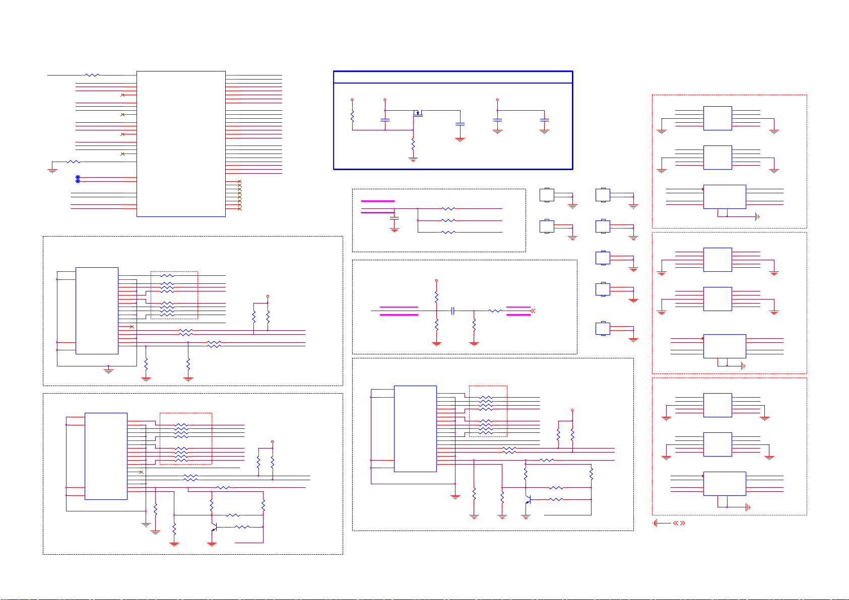
9-4-9 HDMI*
HDMI_CEC
Side HDMI Por t 1 ( HDMI 2.0 )
388G 340F J 05FAT0 0 01: B P R 1.6m m
388G 340F J 05FAT0 0 01: B P R 1.6m m
TP403
TP404
Side H DM I p o r t 2 ( HD M I 2 .0 & H DC P 2 . 2 )
R524
10K 5%
20
22
23
21
8/20 mod ify
HDMI_0_SCL
HDMI_1_SCL
HDMI_2_SCL
HDMI_0_SDA
HDMI_1_SDA
HDMI_2_SDA
HDMI_0_PWR5V
HDMI_1_PWR5V
HDMI_2_PWR5V
HDMI_0_HPD_C BUS
HDMI_1_HPD
HDMI_2_HPD
AVDD105_HDMI_STB
AVDD105_HDMI_STB
AVDD33_HDMI
AVDD33_HDMI
CN501
SHLD0
SHLD2
SHLD3
SHLD1
HDMI 19P
20
22
23
21
R501
100R 5%
MHL_SENSE
REVP
REVN
TMDSD2+
DSHLD0
TMDSD2-
TMDSD1+
DSHLD1
TMDSD1-
TMDSD0+
DSHLD2
TMDSD0-
TMDSC+
CSHLD0
TMDSC-
DDC_GND
CN502
SHLD0
SHLD2
SHLD3
SHLD1
HDMI 19P
CEC
CEC
NC
SCL
SDA
VCC5
HPD
TMDSD2+
DSHLD0
TMDSD2-
TMDSD1+
DSHLD1
TMDSD1-
TMDSD0+
DSHLD2
TMDSD0-
TMDSC+
CSHLD0
TMDSC-
CEC
SDA
DDC_GND
VCC5
HPD
AE29
AG30
AH27
AK29
AL31
AG29
AG27
AL29
AL30
AE28
AH29
AJ29
AM32
AG28
AH28
AJ30
AL32
AD28
AL34
AL33
AM33
AM34
AD25
AD26
1
2
3
4
5
6
7
8
9
10
11
12
13
14
15
16
17
18
19
NC
SCL
U401-6
HDMI_CEC
HDMI_0_SCL
HDMI_1_SCL
HDMI_2_SCL
HDMI_3_SCL
HDMI_0_SDA
HDMI_1_SDA
HDMI_2_SDA
HDMI_3_SDA
HDMI_0_PWR5V
HDMI_1_PWR5V
HDMI_2_PWR5V
HDMI_3_PWR5V
HDMI_0_HPD_C BUS
HDMI_1_HPD
HDMI_2_HPD
HDMI_3_HPD
MHL_SENSE
REVP
REVN
AVDD105_HDMI_STB
AVDD105_HDMI_STB
AVDD33_HDMI
AVDD33_HDMI
MT5806IFEQ
кで皌
稼﹊
90
R540 4R7 5%
R541 4R7 5%
R542 4R7 5%
R543 4R7 5%
R544 4R7 5%
R545 4R7 5%
R546 4R7 5%
R547 4R7 5%
SCL0
SDA0
OPWR0_5V
R523
100K 5%
кで皌
1
2
3
4
5
6
7
8
9
10
11
12
13
14
15
SCL1
16
SDA1
17
18
OPWR1_5V
19
POH_HPD1
稼﹊
90
R590
10K 5%
R515
R516
100R 5%
100R 5%
R548
R549
R551
R550
4R7 5%
4R7 5%
R554
4R7 5%
R552
4R7 5%
R556
R555
4R7 5%
4R7 5%
4R7 5%
4R7 5%
HDMI_0_RX_0
HDMI_0_RX_0B
HDMI_0_RX_1
HDMI_0_RX_1B
HDMI_0_RX_2
HDMI_0_RX_2B
HDMI_0_RX_C
HDMI_0_RX_CB
HDMI_1_RX_0
HDMI_1_RX_0B
HDMI_1_RX_1
HDMI_1_RX_1B
HDMI_1_RX_2
HDMI_1_RX_2B
HDMI_1_RX_C
HDMI_1_RX_CB
HDMI_2_RX_0
HDMI_2_RX_0B
HDMI_2_RX_1
HDMI_2_RX_1B
HDMI_2_RX_2
HDMI_2_RX_2B
HDMI_2_RX_C
HDMI_2_RX_CB
HDMI_3_RX_0
HDMI_3_RX_0B
HDMI_3_RX_1
HDMI_3_RX_1B
HDMI_3_RX_2
HDMI_3_RX_2B
HDMI_3_RX_C
HDMI_3_RX_CB
R511
10K 5%
R8083
R565
100R 5%
100R 5%
R571
100K 5%
AA32
AA31
AA34
AA33
Y34
Y33
AB32
AB31
AD32
AD31
AC32
AC31
AC34
AC33
AE34
AE33
AG34
AG33
AF32
AF31
AE32
AE31
AG32
AG31
AJ32
AJ31
AJ34
AJ33
AH32
AH31
AK32
AK31
RX_0_2
RX_0_2B
RX_0_1
RX_0_1B
RX_0_0
RX_0_0B
RX_0_C
RX_0_CB
HDMI_CEC_0
R509
R521
22R 5%
4R7 5%
RX_1_2
RX_1_2B
RX_1_1
RX_1_1B
RX_1_0
RX_1_0B
RX_1_C
RX_1_CB
HDMI_CEC_1
R572
22R 5%
R569
NC/1K 1/16W 5%
R525
4R7 5%
R570 NC/ 1K 1/16W 5%
Q507
NC/BC 847N3
OPWR0_5V
HDMI_1_HPD
RX_0_0
RX_0_0B
RX_0_1
RX_0_1B
RX_0_2
RX_0_2B
RX_0_C
RX_0_CB
RX_1_0
RX_1_0B
RX_1_1
RX_1_1B
RX_1_2
RX_1_2B
RX_1_C
RX_1_CB
RX_2_0
RX_2_0B
RX_2_1
RX_2_1B
RX_2_2
RX_2_2B
RX_2_C
RX_2_CB
R513
R514
47K 5%
47K 5%
HDMI_0_SCL
HDMI_0_SDA
HDMI_0_PWR5V
HDMI_0_HPD_C BUS
OPWR1_5V
R567
R566
47K 5%
47K 5%
HDMI_1_SCL
HDMI_1_SDA
HDMI_1_PWR 5V
R568
NC/4. 7K1/16W
Anal o g Pow er
+5V_SW
R4314
1K 5%
CEC
HDMI_CEC
Audio Retu r n Ch a n n e l ( A R C)
ARC_HD MI
Bott om H DM I po rt 3 ( AR C / HD MI 1. 4 )
AVDD3V3_SOC
C4524
NC/10nF /16V
6.8PF 0.5 PF 50V
wi th G ND
wi th G ND
CN503
20
SHLD0
22
SHLD2
23
SHLD3
21
SHLD1
HDMI 19P
C506
Q702
AO3414
AVDD33_HDMI AVDD105_HDMI_STB
R4313
100K 5%
wi t h G ND
R505
0R05 1/16W
R504
0R05 1/16W
R503
0R05 1/16W
+5V_SW
R577
47K 5%
C505
1uF 16V
R579
47K 5%
кで皌
稼﹊
90
1
TMDSD2+
2
DSHLD0
3
TMDSD2-
4
TMDSD1+
5
DSHLD1
6
TMDSD1-
7
TMDSD0+
8
DSHLD2
9
TMDSD0-
10
TMDSC+
11
CSHLD0
12
TMDSC-
13
CEC
14
NC
15
SCL
16
SDA
17
DDC_GND
18
VCC5
19
HPD
AVDD105_STB
C4443
100NF 16V
HDMI_CEC _0
HDMI_CEC _1
HDMI_CEC _2
from S ca l er A R C
R530
180 OHM 5%
R529
82R
R557
R558
R559
R560
4R7 5%
4R7 5%
R561
4R7 5%
R562
4R7 5%
R563
R564
4R7 5%
4R7 5%
4R7 5%
4R7 5%
SCL2
R538 100R 5%
SDA2
R539 100R 5%
OPWR2_5V HDMI_2_PWR5V
POH_HPD2
R589
10K 5%
C4446
100NF 16V
wi th G ND
wi th G ND
HDMI_CEC _2
ARC_HD MI
R588
100K 5%
GND3
GASKET
GND6
GASKET
ARC
RX_2_2
RX_2_2B
RX_2_1
RX_2_1B
RX_2_0
RX_2_0B
RX_2_C
RX_2_CB
R574 22R 5%
R575
NC/1K 1/16W 5%
R526 4R7 5%
R576 NC/ 1K 1/16W 5%
Q508
NC/BC 847N3
HDMI_2_HPD
C4518
1uF 16V
1
2
1
2
OPWR2_5V
R536
47K 5%
21
R537
47K 5%
HDMI_2_SCL
HDMI_2_SDA
GND4
1
2
GASKET
GND5
1
2
GASKET
GND7
1
2
GASKET
GND8
1
2
GASKET
GND9
1
2
GASKET
R580
NC/4. 7K1/16W
Clos e t o co n n ec to r
GND
GND
HDMI_CEC _0
SCL0
SDA0
OPWR0_5V
Close to co nn e c to r
GND
GND
HDMI_CEC _1
SCL1
SDA1
OPWR1_5V
Close to co nn e c to r
HDMI_CEC _2
SCL2
SDA2
OPWR2_5V
RX_0_2
RX_0_2B
RX_0_1
RX_0_1B
RX_0_0
RX_0_0B
RX_0_C
RX_0_CB
RX_1_2
RX_1_2B
RX_1_1
RX_1_1B
RX_1_0
RX_1_0B
RX_1_C
RX_1_CB
RX_2_2
RX_2_2B
GND
RX_2_1
RX_2_1B
RX_2_0
RX_2_0B
GND
RX_2_C
RX_2_CB
GND
U506
1
2
3
4
1
2
3
4
U508
AZ1045-04F.R7G
1
2
4
5
1
2
3
4
1
2
3
4
U518
AZ1045-04F.R7G
1
2
4
5
1
2
3
4
1
2
3
4
U511
AZ1045-04F.R7G
1
2
4
5
Line-1
NC
Line-2
NC
GND
GND
Line-3
NC
Line-45NC
AZ1023-04F.R7G
U507
Line-1
NC
Line-2
NC
GND
GND
Line-3
NC
Line-45NC
AZ1023-04F.R7G
IN1
IN2
IN3
IN4
GND
GND
3
8
U516
Line-1
NC
Line-2
NC
GND
GND
Line-3
NC
Line-45NC
AZ1023-04F.R7G
U517
Line-1
NC
Line-2
NC
GND
GND
Line-3
NC
Line-45NC
AZ1023-04F.R7G
IN1
IN2
IN3
IN4
GND
GND
3
8
U509
Line-1
NC
Line-2
NC
GND
GND
Line-3
NC
Line-45NC
AZ1023-04F.R7G
U510
Line-1
NC
Line-2
NC
GND
GND
Line-3
NC
Line-45NC
AZ1023-04F.R7G
IN1
IN2
IN3
IN4
GND
GND
3
8
10
9
8
7
6
10
9
8
7
6
NC
NC
NC
NC
10
9
8
7
6
10
9
8
7
6
NC
NC
NC
NC
10
9
8
7
6
10
9
8
7
6
NC
NC
NC
NC
RX_0_2
RX_0_2B
RX_0_1
RX_0_1B
RX_0_0
RX_0_0B
RX_0_C
RX_0_CB
10
9
7
6
RX_1_2
RX_1_2B
RX_1_1
RX_1_1B
RX_1_0
RX_1_0B
RX_1_C
RX_1_CB
10
9
7
6
RX_2_2
RX_2_2B
RX_2_1
RX_2_1B
RX_2_0
RX_2_0B
RX_2_C
RX_2_CB
10
9
7
6
OPWR0_5V
4,5,6,7, 8,9,10,11,13,14,1 5,16,17,18,19,20, 21,22
HDMI_CEC _0
SCL0
SDA0
HDMI_CEC _1
SCL1
SDA1
OPWR1_5V
HDMI_CEC _2
SCL2
SDA2
OPWR2_5V
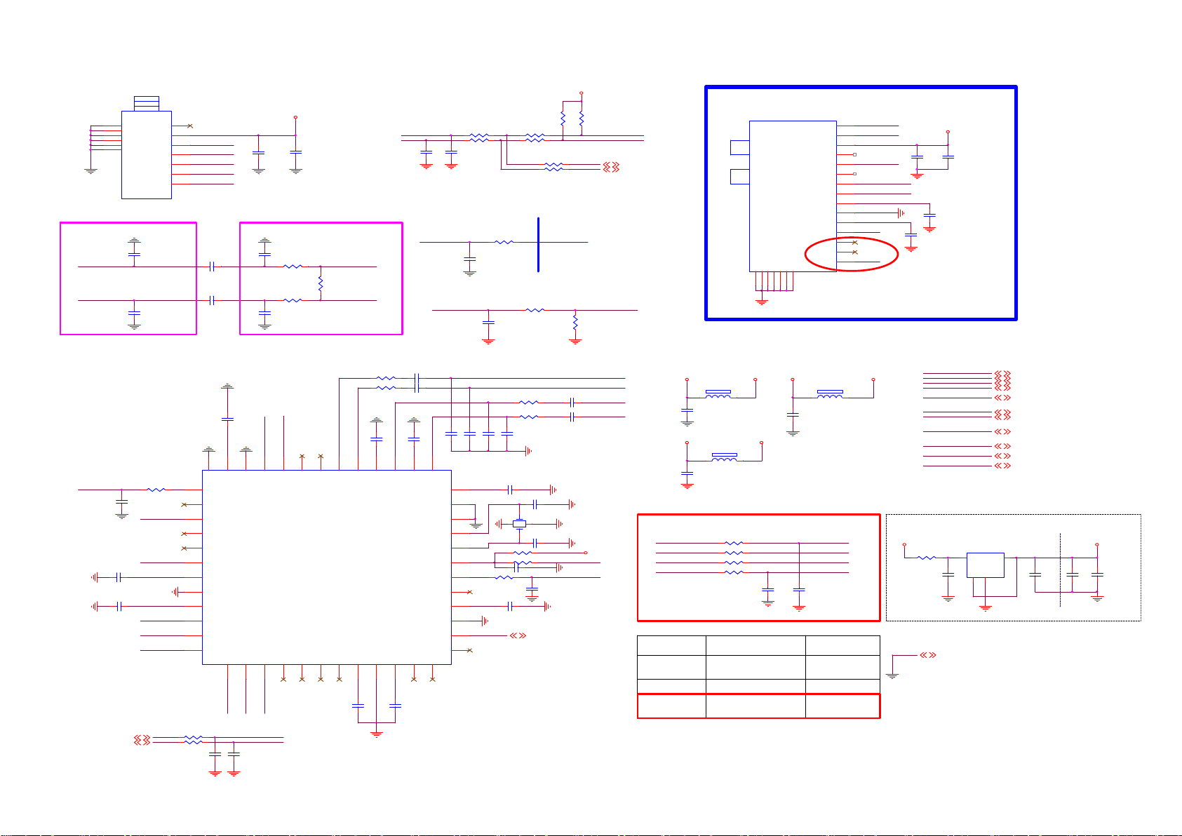
9-4-10 Tuner & Demod*
TU203
8
TH1
9
TH2
10
+B1(+3.3V)
TH3
11
TH4
12
TH5
13
TH6
CLO SE TO TUNER Close to S caler (U401)
C
C
TUN_DIF-_D EMOD
TUN_DIF+_D EMOD
TUN_DIF-#T2
TUN_DIF+#T2
Demo d
IF_AGC_S2_TUNER
C121
100NF 16V
13_18V_SW
DISEQC_OUT
C107
100NF 16V
C140
100NF 16V
TS_T2_VAL
T2 DE MOD I2C
From MT 5 8 06
9,13
9,13
OSCL2
OSDA2
T2 T U NE R
1
Ant. PWR
2
3
TUN_SDA
SDA
4
TUN_SCL
SCL
5
DIF(N)
IF AGC
C142
10PF 50V
TUN_DIF-#T2
6
TUN_DIF+#T2
DIF(P)
7
IF_AGC_T TUN_DIF-#T2
C106
100NF 16V
C119
C150
10PF 50V
100NF 16V
C134
100NF 16V
+1.2V_T2
48
49
R150
4K7 5%
+1.2V_T2
+3.3V_T2 +1.2V_T2
DEMOD_SCL
DEMOD_SDA
EPad
1
MP_A
VDD_Vcore
2
MP_B
3
GPIO_0
4
DISEQC_CMD
5
DISEQC_IN
6
DISEQC_OUT
7
VDD_Vcore
8
GND
9
VDD_VIO
10
SCL_Host
11
SDA_Host
12
TS_VLD
TS_SYNC13TS_CLK14TS_D0/SER15TS_D116TS_D217TS_D318TS_D419VDD_Vcore20GND21VDD_VIO22TSD523TSD6
TS_T2_SYNC
R148
R149
33R 5%
C101
C102
100pF 50V
33R 5%
S2T2_TUN_SCL
46
47
GND
TS_T2_DQ0
TS_T2_CLK
TO Demod
DEMOD_SCL
DEMOD_SDA
100pF 50V
C118
100NF 16V
C155
NC/10PF 50V
R151
R152
C113
NC/10PF 50V
S2T2_TUN_SDA
45
SCL_T
+3V3_TUNER
C133
10uF 6.3V
0R05 1/16W
0R05 1/16W
44
SDA_T
CLK_IN_OUT
SI2169-D60-GMR
R153
NC/620R 1/16W 5%
U718
TU_FAT_IN2-
TU_FAT_IN2+
41
42NC43
RC_ADC_N
+1.2V_T2
R168
R169
0R05 1/16W
0R05 1/16W
40
TC_ADC_P
C147
100NF 16V
TUNER I2C
C117
100NF 16V
39
S_ADC_QN
+3.3V_T2
R134
TUN_SCL
TUN_SDA
C149
IF_AGC_T IF_AGCT
R135
100R 5%
C183
100pF 50V
100pF 50V
100R 5%
Wri te:0x C 0
Read:0xC1
CLOSE T O T u ne r
C116
47nF 50V
CLOSE T O T u n er
R132
10K 5%
IF_AGC_T T2_IF_AGC_TUNER
C185
10NF 50V
C182 100N F 16V
C105 100N F 16V
R127
R129
C145
C104
C144
C137
NC/10PF 50V
NC/10PF 50V
36
35
34
33
32
31
30
29
28
27
26
25
NC/10PF 50V
+3.3VA_T2
2 4
R119 NC/4K7 1/16W 5%
R120 22R 5%
C181 100N F 16V
R121
4K7 5%
LNB_EN
C153
100NF 16V
38
VDD_Vana
S_ADC_IN
S_ADC_QP
XTAL_I/CLK_IN
VDD_Vcore
TS_ERR/GPIO_1
37
S_ADC_IP
GND
ADDR
XTAL_O
RESETB
MP_D
MP_C
GND
TSD7
24
C103
100NF 16V
R136
R137
NC/10PF 50V
C184
100NF 16V
1
3
C146
100NF 16V
0R05 1/10W
0R05 1/10W
R138
R139
NC/0R05 1/10W
NC/0R05 1/10W
R130
4K7 5%
51 OHM 5%
51 OHM 5%
C148
3.3PF 0.25PF 50V
X402
16MHz
C136
3.3PF 0.25PF 50V
T2_IF_AGC_TUNER
C151
100NF 16V
LNB_EN
+3V3_TUNER
R141
R140
From MT 5 8 06
From T2 d emod
NC/22K 1/ 16W 5%
TUN_DIF+_D EMOD
TUN_DIF-_D EMOD
C180
100NF 16V
C143
100NF 16V
DEMOD_RESET
14
4K7 5%
4K7 5%
S2T2_TUN_SCL
S2T2_TUN_SDA
From T2 D emod
From M T5806 (OSD A2 )
R131
+3.3V_T2
T2/ S2 TUNE R
TU202
9,13
OSCL2
9,13
OSDA2
C139
10PF 50V
TH116TH217TH318TH419TH520TH621TH7
22
DEMO D PO WER
+1.2V_T2
QP
IP
1 2
C132
10uF 6.3V
+3.3V_T2
C179
10uF 6.3V
TS_T2_SYNC
TS_T2_VAL
TS_T2_CLK
Model
T (T2 )
K (S2)
S (T2/ S 2)
AVDD1V2
FB717
120R 3A
DVDD3V3
FB718
120R 3A
1 2
R122 22R 5%
R123 22R 5%
R124 22R 5%
R125 22R 5%
Demo d
T2 Si2168
356G05 750486 10
Si2166
Si2169
356G05 750486 13
SCL
SDA
+3.3V
NC 1
IF_AGC
NC 2
IF(N)
IF(P)
LNB
GND
SAT_AGC
I(P)
NC 3
NC 4
Q(N)
TDJA-G661D
FB719
1 2
120R 3A
C138
10uF 6.3V
DEMOD_TS0TS_T2_DQ0
DEMOD_TSSYNC
DEMOD_TSVAL
DEMOD_TSCLK
C135
10PF 50V
Tuner
TU203
TU202
1
2
3
4
5
6
7
8
26
27
58
59
60
61
62
Mod i fy 06 12
TUN_SCL
TUN_SDA
+3V3_VCC_S2
IF_AGC_T
TUN_DIF+#T2
TUNER_LNB
IF_AGC_S2_TUNER
IP
QP
DVDD3V3+3.3VA_T2
+5V_SW TO TUNER 3 . 3V
C123
100NF 16V
CLOS E TO TUNER
C125
1nF 50V
13_18V_SW
R154
0 OHM 1/8W
+3V3_TUNER
C122
10uF 6.3V
C124
1nF 50V
DEMOD_TSSYNC
DEMOD_TSVAL
DEMOD_TSCLK
DEMOD_TS0
IF_AGCT
TU_FAT_IN2+
TU_FAT_IN2-
TUNER_LNB
DISEQC_OUT
DEMOD_RESET
U719
G960T63Uf
3
C126
1UF 50V
GND
DEMOD_TSSYNC17
DEMOD_TSVAL 17
DEMOD_TSCLK17
DEMOD_TS0 17
IF_AGCT
TU_FAT_IN2+
TU_FAT_IN2-
13_18V_SW
TUNER_LNB
DISEQC_OUT
DEMOD_RESET 17
2
VOUT
VIN
GND14
4
9
9
9
14
14
14
C128
10uF 6.3V
Close to t uner
4,5,6,7,8, 9,10,11,12,14,15, 16,17,18,19,20,21, 22
C127
1UF 50V
+3V3_TUNER+5V_SW
C129
100NF 16V

9-4-11 LNB & EXT AV INPUT
Main_12V
C250
100NF 25V
Main_12V
C253 3.3NF 50V
LNB_EN
LINEDR OP
13_18V_SW
LNB P O W E R SUPP L Y
DVDD 3V3
R718
10K 5%
LNB_EN 13_18V_SW
R719
NC/ 100K 1/16W 5%
LNB_ E N :
Low: disabl e
High: enabl e
MP8124 Enable Selection
C249 220nF 16V
R227 60. 4K 1%
R214
R215
R218
DVDD 3V3
R720
10K 5%
LINEDR OP
R721
NC/ 100K 1/16W 5%
LIN E D R O P:
Low: 13.3/18.3V
High: 14.3/19.3V
Compensation Selection
0R05 1/16W
0R05 1/16W
0R05 1/16W
L201
10uH
C298
10uF 16V
U202
8
AGND
11
BYPASS
12
VDD
10
COMP
2
EN
1
LINEDR OP
13V/18V14EXTM
MP8124GD Z
DVDD 3V3
R774
10K 5%
R780
NC/ 100K 1/16W 5%
13_1 8V_SW
High: 18V
Low: 13V
PGND
VBOOST
VOUT
TCAP
D505
1 2
4
3
SW
5
BST
6
7
9
13
SR24
C248
100NF 25V
C245 22NF25V
R224 33 OHM
R213
100K 1%
C243
10uF 25V
C240
C244
10uF 25V
10uF 25V
ESD & S u rg e
Protect
D504
SR24
1 2
C297
100NF 25V R221
1 2
D503
SR24
ZD201
1 2
DISEQC_OU T
R216
NC/PJSD24CW
R220
3K
3K
Mo d ify 0 4/19
R217
3K
ZD202
PJSD24CW
1 2
33K 1%
R225
5.1K 1%
TUNER_LNB
TUN_LNB
ZD203
NC/PJSD24CW
1 2
6,22
6,22
U0TX
U0RX
TUNER_LNB
TUN_LNB
DISEQC_OU T
LNB_EN
LINEDR OP
13_18V_SW
U0TX
U0RX
GND
Res e rve r for A P/LT
TUNER_LNB
TUN_LNB
DISEQC_OU T
LNB_EN
LINEDR OP
13_18V_SW
R4010
R4011
NC/ 100R 1/16W 5%
NC/ 100R 1/16W 5%
13
17
13
13
17
13
4,5,6, 7,8,9,10,11,12, 13,15,16,17,18,19, 20,21,22
45
SOC-TX-SERVICE
SOC-RX-SERVICE
12
12
ZD130
ZD145
NC/MLVG0402
NC/MLVG0402
1
2
3
CN130
NC/ CONN
Res e rve r for A P /LT
CN132
NC/ PHONE JACK 7P
NC/ 0R05 1/10W
C8171
NC/ 10PF 50V
wi th G ND
C l o s e t o C N 1 0 1
R8076
R8077
NC/ 0R05 1/10W
R8078
NC/ 0R05 1/10W
wi th GND
R8079
NC/ 0R05 1/10W
SOY_EXT
COM0_EXT
PB0P_EXT
PR0P_EXT
9
9
9
9
NEAR CO NNECT O R
R8075
NC/ 0R05 1/10W
wi th G ND
R8070
NC/ 75R 1/16W 1%
4
Y-IN -0
2
PB-IN-0
5
3
PR-IN-0
6
12
7
1
ZD7516
NC/TVM1G5R5M100R
12
ZD7515
NC/TVM1G5R5M100R
12
ZD7514
R8073
NC/ 0R05 1/10W
NC/TVM1G5R5M100R
R8074
wi th GND
R8071
NC/ 75R 1/16W 1%
R8072
NC/ 75R 1/16W 1%
C8172
NC/10PF 50V
C8170
NC/10PF 50V
NC/ 0R05 1/10W
AV I n pu t
Res e rve r for A P /LT
CN133
A
B
C
NC/ RCA JACK
388G 07 8 G1 3 7 AC L 00 0 1
Clo s e to CO N NECTO R
2
1
4
YPbPr_L
3
6
YPbPr_R
12
ZD7517
NC/ MLVG0402
C8173
NC/ 10PF 50V
R8065
NC/ 75R 1/16W 1%
Clo s e to S o C
R8067
CVBS0P_EXT
NC/ 100R 1/16W 5%
CVBS0P_EXT
9
5
wi th G ND
AIN_L0
AIN_R0
wi th GND
AIN_L0
AIN_R0
Near Sca ler
9,21
9,21
12
ZD7519
NC/ MLVG0402
12
ZD7518
NC/ MLVG0402
C8166
NC/ 1nF 50V
C8168 NC /1uF 10V
C8167 NC /1uF 10V
C8165
NC/ 1nF 50V
R8069
R8068
NC/ 30K OHM +-1% 1/16W
NC/ 30K OHM +-1% 1/16W

9-4-12 Internal CI
CLOS E T O C I C O NN E CT O R
+5V_SW
CI_PW R_EN
C173
1UF 50 V
CI_ P W R_E N
H:EN
L: OF F
CI_D 3
CI_D 4
CI_D 5
CI_D 6
CI_D 7
CI_C E1#
CI_A10
CI_OE#
CI_A11
CI_A9
CI_A8
CI_A13
CI_A14
CI_WE#
CI2_VCC
CI2_VCC
CI_IR EQ#
CI_MIVAL_R
CI_MCLKI_R
CI_A12
CI_A7
CI_A6
CI_A5
CI_A4
CI_A3
CI_A2
CI_A1
CI_A0
CI_D 0
CI_D 1
CI_D 2
U711
G524D3T11U
5
VOUT
IN
4
FLG
EN
GND
2
R1195
4K7 5%
CN159 PCMICA C ARD
1
GND
2
D3
3
D4
4
D5
5
D6
6
D7
7
CE1#
8
A10
9
OE#
10
A11
11
A9
12
A8
13
A13
14
A14
15
WE#
16
READY #:IREQ#
17
VCC
18
VPP1
19
A16
20
A15
21
A12
22
A7
23
A6
24
A5
25
A4
26
A3
27
A2
28
A1
29
A0
30
D0
31
D1
32
D2
33
WP#
34
GND
CI_C D1#
CI_C D2#
CI_I ORD#
CI_I OWR#
CI_R EG#
CI_C E1#
CI_OE#
CI_W E#
CI_I REQ#
CI_W AIT#
CI_VS1#
CI_R ESET
CI_D VDD3V3
R1196
10K 5%
1
R142 0R05
3
CI_OCP
HI = > NO RM AL
LO => O C
CI Slo t
GND
CD1#
D11
D12
D13
D14
D15
CE2#
VS1#
IORD #
IOWR#
A17
A18
A19
A20
PCM CIA
69697070717172
A21
VCC
VPP2
A22
A23
A24
A25
VS2#
RESET
WAIT#
INPAC K
REG#
BVD2#:SPKR
BVD1#:STSCHG
D10
CD2#
GND
D8
D9
72
R1141 0R05 1/ 16W
R1142 0R05 1/ 16W
R1143 0R05 1/ 16W
R1144 0R05 1/ 16W
R1145 0R05 1/ 16W
R1146 0R05 1/ 16W
R1147 0R05 1/ 16W
R1148 0R05 1/ 16W
R1149 0R05 1/ 16W
R1150 0R05 1/ 16W
R1151 0R05 1/ 16W
R1152 0R05 1/ 16W
Clo s e d t o CI SL O T
35
36
37
38
39
40
41
42
43
44
45
46
47
48
49
50
51
52
53
54
55
56
57
58
59
60
61
62
63
64
65
66
67
68
C172
10uF 16V
CI_C D1#
CI_MDO3_R
CI_MDO4_R
CI_MDO5_R
CI_MDO6_R
CI_MDO7_R
CI_C E2#
CI_VS1#
CI_I ORD#
CI_I OWR#
CI_MISTRT_R
CI_MDI 0_R
CI_MDI 1_R
CI_MDI 2_R
CI_MDI 3_R
CI_MDI 4_R
CI_MDI 5_R
CI_MDI 6_R
CI_MDI 7_R
CI_MCLKO_R
CI_R ESET
CI_WAI T#
CI_R EG#
CI_MOVAL_R
CI_MOSTRT_R
CI_MDO0_R
CI_MDO1_R
CI_MDO2_R
CI_C D2#
SPI_CLK
SPI_CLK1
SPI_DATA
SPI_CLE
CI_IN T
CI_TSCLK
CI_TSVAL
CI_TSSYN C
PVR_TSDATA0
PVR_TSDATA1
PVR_TSVAL
CI_R ST
CI2_VC C
C186
10uF 16V
C174
100NF 16V
CI2_VCC
CI2_VCC
CI_D VDD3V3
R1187
10K 5%
CI_C D1#
C169
100NF 16V
CI_D VDD3V3 CI2_VC C
R1188
10K 5%
CI_C D2#
C170
100NF 16V
Clo s ed t o CI Co n n ect o r
CI_MDI 5
CI_MDI 4
CI_MIVAL
CI_MDI 3
CI_MISTRT
CI_MDI 0
CI_MDI 1
CI_MDI 2
CI_MDI 6
CI_MDI 7
wi th GND
PVR_TSCLK
CI_TSDATA0
CI_MDO0
CI_MDO1
CI_MDO2
CI_MDO3
CI_MDO4
CI_MDO5
CI_MDO6
CI_MDO7
PVR_TSSYNC CI_MCLKO_R
Mo dif y by EM I
C188
10PF 50V
Clo s e d t o M ai n Chi p
CI_D VDD3V3
R1189
10K 5%
CI_VS1#
R1153 47R 5%
R1154 47R 5%
R1155 47R 5%
R1156 47R 5%
R1157 47R 5%
R1158 47R 5%
R1159 47R 5%
R1160 47R 5%
R1161 47R 5%
R1162 47R 5%
R1163 47R 5%
Clo s e d t o U4 0 1
R1164 47R 5%
R1165 47R 5%
R1166 47R 5%
R1167 47R 5%
R1168 47R 5%
R1169 47R 5%
R1170 47R 5%
R1171 47R 5%
R1172 47R 5%
R1173 47R 5%
R1174 47R 5%
Clo s e d t o CI SL O T
R1190
10K 5%
CI_W AIT#
CI2_VCC
R1192
10K 5%
CI_I REQ#
DVDD 3V3
CI_MDI 5_R
CI_MDI 4_R
CI_MIVAL_R
CI_MDI 3_R
CI_MISTRT_R
CI_MDI 0_R
CI_MDI 1_R
CI_MDI 2_R
CI_MDI 6_R
CI_MDI 7_R
CI_MCLKI_RCI_MCLKI
CI_MOVAL_R
CI_MOSTRT_R
CI_MDO0_R
CI_MDO1_R
CI_MDO2_R
CI_MDO3_R
CI_MDO4_R
CI_MDO5_R
CI_MDO6_R
CI_MDO7_R
R1194
Clos ed t o CI SL O T
0R05 1/ 10W
Mo dif y by EM I
C187
10PF 50V
w i th GND
CI2_VCC
R1191
10K 5%
CI_C E2#
CI_D VDD3V3
6/24
C171
100NF 16V
Cont r ol I n te r f ac e
GND
CI_OCP
CI_PWR _EN
CI_A0
CI_A1
CI_A2
CI_A3
CI_A4
CI_A5
CI_A6
CI_A7
CI_A8
CI_A9
CI_A10
CI_A11
CI_A12
CI_A13
CI_A14
CI_MCLKI
CI_MIVAL
CI_MISTRT
CI_MDI 0
CI_MDI 1
CI_MDI 2
CI_MDI 3
CI_MDI 4
CI_MDI 5
CI_MDI 6
CI_MDI 7
CI_D 0
CI_D 1
CI_D 2
CI_D 3
CI_D 4
CI_D 5
CI_D 6
CI_D 7
CI_MDO0
CI_MDO1
CI_MDO2
CI_MDO3
CI_MDO4
CI_MDO5
CI_MDO6
CI_MDO7
SPI_CLK
SPI_CLK1
SPI_DATA
SPI_CLE
CI_IN T
CI_TSCLK
CI_TSVAL
CI_TSSYN C
CI_TSDATA0
PVR_TSSYNC
PVR_TSCLK
PVR_TSDATA0
PVR_TSDATA1
PVR_TSVAL
CI_R ST
4,5,6,7, 8,9,10,11,12,13 ,14,16,17,18,19,20, 21,22
CI_OCP
CI_PW R_EN
CI_A0
CI_A1
CI_A2
CI_A3
CI_A4
CI_A5
CI_A6
CI_A7
CI_A8
CI_A9
CI_A10
CI_A11
CI_A12
CI_A13
CI_A14
CI_MCLKI
CI_MIVAL
CI_MISTRT
CI_MDI 0
CI_MDI 1
CI_MDI 2
CI_MDI 3
CI_MDI 4
CI_MDI 5
CI_MDI 6
CI_MDI 7
CI_D 0
CI_D 1
CI_D 2
CI_D 3
CI_D 4
CI_D 5
CI_D 6
CI_D 7
CI_MDO0
CI_MDO1
CI_MDO2
CI_MDO3
CI_MDO4
CI_MDO5
CI_MDO6
CI_MDO7
SPI_CLK
SPI_CLK1
SPI_DATA
SPI_CLE
CI_I NT
CI_TSCLK
CI_TSVAL
CI_TSSY NC
CI_TSDATA0
PVR_TSSYNC
PVR_TSCLK
PVR_TSDATA0
PVR_TSDATA1
PVR_TSVAL
CI_R ST
17
17
17
17
17
17
17
17
17
17
17
17
17
17
17
17
17
17
17
17
17
17
17
17
17
17
17
17
17
17
17
17
17
17
17
17
17
17
17
17
17
17
17
17
17
17
17
17
17
17
17
17
17
17
17
17
17
17
17

9-4-13 WIFI/KEYPAD
IR/ KE Y B O AR D
8/2 0 O TS Key
LED_PWM2
LED_PWM0
RC6
POWER_KEY
IR_SSB
IR_R C
8/2 0 P H P SR
WI FI PW R CO NTRO L
WIF I_PWR_EN
Wi- Fi _ PW R_ E N :
Enable : High
Disable : Low
BT P W R C ONT RO L
R113
100R 1%
R163
6K8 1%
+5V_STB
R404
R1197
10K 5%
C194
100pF 50V
C4297
10uF 16V
100R 5%
3V3SB
R109
R108
NC/ 6K8 1%
10K 1%
R118 100R 5%
R117 100R 5%
R112 100R 5%
C108
C156
NC/ 100pF 50V
100pF 50V
R171 NC /0 OHM 1/8W
U714
G524D3T11U
5
IN
4
EN
R105 0R05 1/16W
R170 NC /100R 1/16W 1%
C112
100pF 50V
Mo dif y b y EM I
VOUT
GND
2
FLG
1
3
R1198
10K 5%
8/2 0 O TS Key
Wi-Fi_VCC
C157
100NF 16V
C4265
10uF 16V
C158
100NF 16V
Wi-Fi_VC C
C4263
10uF 25V
12
ZD125
AZ5123-01H.R 7G
EMI & ES D s ol u ti o n
C4266
100NF 16V
LED_GE
LED_RE
IR
KEY1_INKEY_PAD0
KEY2_IN
12
ZD126
NC/ AZ5123-01H
3V3SB
12
ZD128
AZ5123-01H. R7G
WIF I_RSTn
12
FB403
30R/600mA
C195
100NF 16V
C114
NC/ 10PF 50V
CN401
1
3
5
7
9
CONN
CN415 CONN
2
4
6
8
2
4
6
8
10
Gr ound i ng( 20m il )
C115
NC/ 10PF 50V
GND
6,22
IR_SSB
6,22
IR_R C
17
17,22
6,17
LED_PWM0
6,17
LED_PWM2
6,22
RC6
17
WoWLAN _IRQ
17
WIF I_PWR_EN
WIF I_RESET17
18
USB_DP_P3
18
USB_DM_P3
BT_IRQ
USB_DP_P1
USB_DM_P1
BTI_PWR_EN
LED_RE
IR
L103
90OHM
1
R4267
4
R4268
2R2 5%
2R2 5%
USB_DP_P3
USB_DM_P3
2
3
311 G W 2 0 0C08 ABL
WIF I_RESET
1
3
5
7
Wi-Fi_VCC
WoWLAN_I RQn
Wi-Fi_VCC
4,5,6, 7,8,9 ,10,11,12,13,14, 15,17,18, 19,20,21,22
IR_SSB
IR_R C
POWER_KEY
KEY_PAD0
POWER_KEY
KEY_PAD 0
LED_PWM0
LED_PWM2
RC6
WoWLAN _IRQ
WIF I_PWR_EN
WIF I_RESET
USB_DP_P3
USB_DM_P3
BT_IRQ
USB_DP_P1
USB_DM_P1
BTI_PWR_EN
LED_RE
IR
3V3SB
R5116
R5115
100R 5%
NC/ 10K 1/16W 5%
R5117
NC/ 10K 1/16W 5%
17
18
18
17
22
22
WIF I_RSTn
WoWLAN _IRQ
R4273
100R 5%
3V3SB
R5100
NC/ 10K 1/16W 5%
WoWLAN _IRQn
R5103
NC/ 10K 1/16W 5%
3V3SB
+5V_STB
+5V_SW
BTI_PWR_EN
BT_P W R _E N :
Enable : High
Disable : Low
R183 NC /0R05 1/8W
R184
0 OHM 1/ 8W
R187
10K 5%
C176
10uF 25V
R186
100R 5%
U715
G524D3T11U
5
IN
4
EN
VOUT
GND
2
FLG
R185
NC/ 0 OHM 1/8W
1
3
R189
10K 5%
C177
10uF 16V
+5V_BT
C175
10uF 16V
+5V_BT
C178
100NF 16V
FO R BT CO NNECTO R
910
CN417
1
2
3
4
5
6
7
8
CONN
R182 0 OH M 1/8W
R103
BT_RSTn
IR_R C
10R 5%
C4036
+5V_BT
C4037
NC/ 10PF 50V
NC/ 10PF 50V
3
2
L4104
90OHM
4
1
R181
R180
2R2 5%
2R2 5%
USB_DM_P1
USB_DP_P1
17
BT_RESET
BT_RESET
R174
100R 5%
R175
NC/ 100R 1/ 16W 5%
R172
NC/ 10K 1/16W 5%
BT_RSTn
R173
NC/ 10K 1/16W 5%
BT_IRQnBT_IRQ
TP33
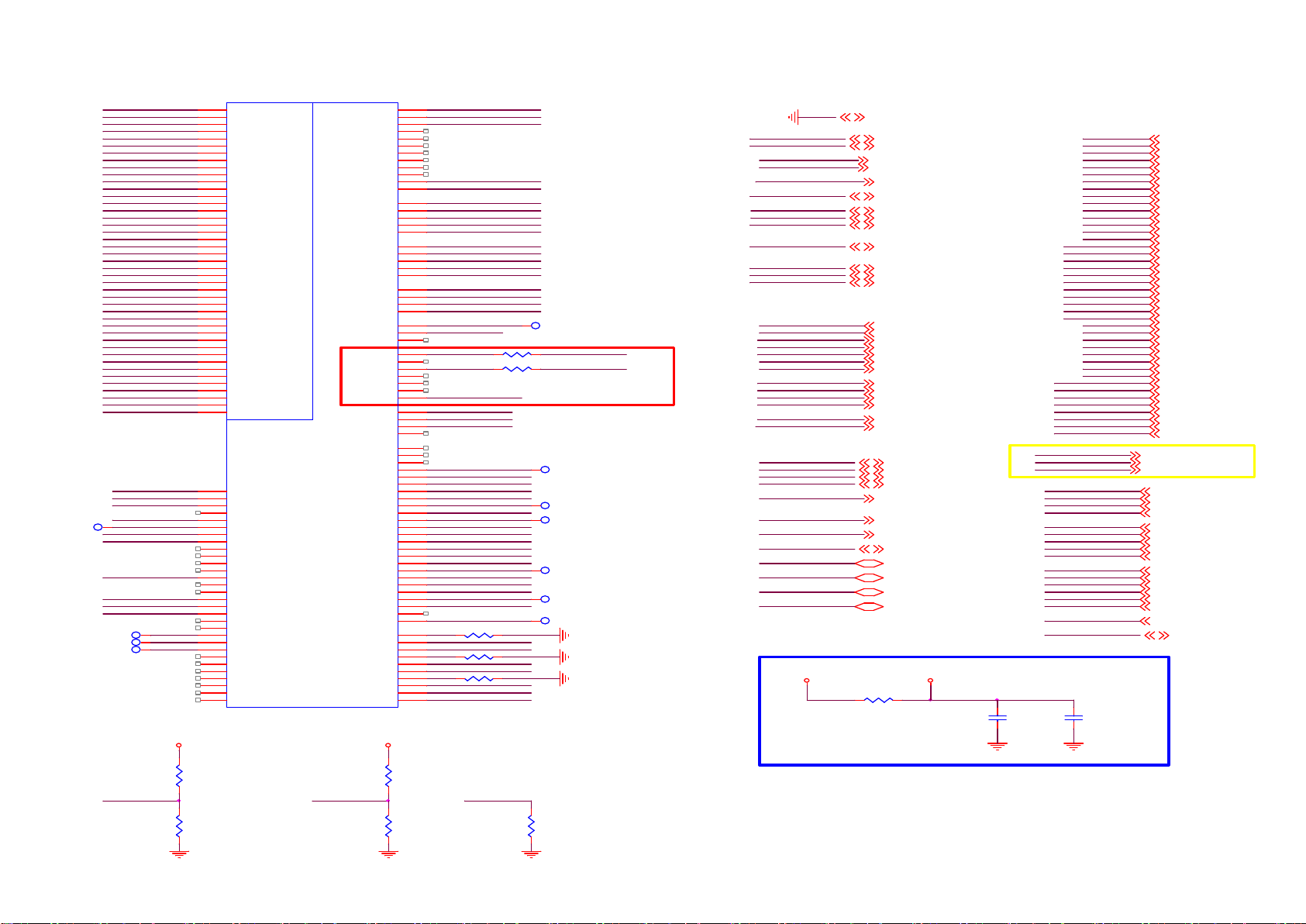
9-4-14 GPIO/ServAD
CI_A0
CI_A1
CI_A2
CI_A3
CI_A4
CI_A5
CI_A6
CI_A7
CI_A8
CI_A9
CI_A10
CI_A11
CI_A12
CI_A13
CI_A14
CI_MCLKI
CI_MIVAL
CI_MISTRT
CI_MDI0
CI_MDI1
CI_MDI2
CI_MDI3
CI_MDI4
CI_MDI5
CI_MDI6
CI_MDI7
CI_D 0
CI_D 1
CI_D 2
CI_D 3
CI_D 4
CI_D 5
CI_D 6
CI_D 7
CI_MDO0
CI_MDO1
CI_MDO2
CI_MDO3
CI_MDO4
CI_MDO5
CI_MDO6
CI_MDO7
CI_R ST
USB_EN_P0
USB_EN_P1
CI_PWR _EN
TP437
CI_OCP
HTPDn
LOCKn
LINEDR OP
VIDEO_DET
YPBPR_D ETECT1
I2SAMP_RESET
TP2
TP3
TP4
Main_12V
J30
H29
E29
A30
B30
A31
C30
B31
G33
H32
J34
J32
B33
G32
F33
B34
C33
G34
F34
F32
E32
D34
C34
C32
B32
A32
J29
G29
F31
N29
P27
L27
K33
L31
G31
G30
F30
N28
N27
L28
K28
J33
K30
L32
T27
P28
E31
F29
L33
AF7
AG7
AF6
AE8
AC6
AC7
AC5
AN4
AP4
AN5
AP5
AN6
E30
AA30
L34
P29
D30
R27
AP3
AN2
AN3
AF8
AG5
AF5
U401-8
CI_A0
CI_A1
CI_A2
CI_A3
CI_A4
CI_A5
CI_A6
CI_A7
CI_A8
CI_A9
CI_A10
CI_A11
CI_A12
CI_A13
CI_A14
CI_MCLKI
CI_MIVAL
CI_MISTRT
CI_MDI0
CI_MDI1
CI_MDI2
CI_MDI3
CI_MDI4
CI_MDI5
CI_MDI6
CI_MDI7
CI_D0
CI_D1
CI_D2
CI_D3
CI_D4
CI_D5
CI_D6
CI_D7
CI_MDO0
CI_MDO1
CI_MDO2
CI_MDO3
CI_MDO4
CI_MDO5
CI_MDO6
CI_MDO7
CI_RST
GPIO42
GPIO43
GPIO44
GPIO45
GPIO46
GPIO48
GPIO49
GPIO50
GPIO51
GPIO52
GPIO53
GPIO54
GPIO55
GPIO56
GPIO57
GPIO58
GPIO59
GPIO60
GPIO61
GPIO62
GPIO63
GPIO64
GPIO65
GPIO66
GPIO67
GPIO68
GPIO69
GPIO70
GPIO71
GPIO72
MT5806IFEQ
GPIO 0
GPIO 1
GPIO 2
GPIO 3
GPIO 4
GPIO 5
GPIO 6
GPIO 7
GPIO 8
GPIO 9
GPIO 1 0
GPIO 1 1
GPIO 1 2
GPIO 1 3
GPIO 1 4
GPIO 1 5
GPIO 1 6
GPIO 1 7
GPIO 1 8
GPIO 1 9
GPIO 2 0
GPIO 2 1
GPIO 2 2
GPIO 2 3
GPIO 2 4
GPIO 2 5
GPIO 2 6
GPIO 2 7
GPIO 2 8
GPIO 2 9
GPIO 3 0
GPIO 3 1
GPIO 3 2
GPIO 3 3
GPIO 3 4
GPIO 3 5
GPIO 3 6
GPIO 3 7
GPIO 3 8
GPIO 3 9
GPIO 4 0
GPIO 4 1
GPIO 4 7
DEMOD_RST
DEMOD_TSCLK
DEMOD_TSDATA0
DEMOD_TSDATA1
DEMOD_TSDATA2
DEMOD_TSDATA3
DEMOD_TSDATA4
DEMOD_TSDATA5
DEMOD_TSDATA6
DEMOD_TSDATA7
DEMOD_TSSYNC
DEMOD_TSVAL
CI_IN T
CI_TSCLK
CI_TSDATA0
CI_TSSYN C
CI_TSVAL
PVR_TSCLK
PVR_TSVAL
PVR_TSSYNC
PVR_TSDATA0
PVR_TSDATA1
SPI_CLK1
SPI_CLK
SPI_DATA
SPI_CLE
OPWM0
OPWM1
OPWM2
SD_D0
SD_D1
SD_D2
SD_D3
SD_CMD
SD_CLK
DVDD33_SD
LED_PWM0
LED_PWM1
LED_PWM2
LED_PWM3
OPCTRL0
OPCTRL1
OPCTRL2
OPCTRL3
OPCTRL4
OPCTRL5
OPCTRL6
OPCTRL7
OPCTRL8
OPCTRL9
OPCTRL10
OPCTRL11
OPCTRL12
OPCTRL13
OPCTRL14
OPCTRL15
OPCTRL16
OPCTRL17
OPCTRL18
OPCTRL19
OPCTRL20
OPCTRL21
OPCTRL22
OPCTRL23
OPCTRL24
ADIN 0_SRV
ADIN 1_SRV
ADIN 2_SRV
ADIN 3_SRV
ADIN 4_SRV
ADIN 5_SRV
ADIN 6_SRV
ADIN 7_SRV
ADIN 8_SRV
ADIN 9_SRV
Panel_12V
Y30
AA28
Y27
AA29
AB29
AB28
AB27
AC27
AC29
AC28
AA27
Y28
K31
N30
H30
E33
K29
C31
L29
L30
D33
J31
D32
P30
K32
H31
AP8
AE7
AN8
N32
N33
M32
M33
P33
P34
M34
AH15
AG15
AG16
AH16
AJ20
AH19
AN23
AG19
AJ17
AF18
AG20
AJ18
AH20
AJ16
AL19
AG17
AG12
AK12
AJ11
AJ12
AH12
AG14
AL11
AL12
AK11
AB8
AB9
AC8
AC9
AL23
AP23
AK23
AM31
AM24
AK19
AK25
AK14
AP24
AN24
DEMOD_RESET
DEMOD_TSCLK
DEMOD_TS0
DEMOD_TSSYNC
DEMOD_TSVAL
CI_IN T
CI_TSCLK
CI_TSDATA0
CI_TSSYN C
CI_TSVAL
PVR_TSCLK
PVR_TSVAL
PVR_TSSYNC
PVR_TSDATA0
PVR_TSDATA1
SPI_CLK1
SPI_CLK
SPI_DATA
SPI_CLE
A_DIM_ADJ
SD_D0
R451
SD_D2
R452
DVDD33_SD
LED_PWM0
LED_PWM1
LED_PWM2
FB_PWR_C TRL
INV_EN
AMP_PWRDN
HP_DET
SYS_EEPROM_WP
PANEL_PWR_EN
USB_EN_P2
MUTE_CTL
PMIC_INT
DDR_VTT_CTRL
BT_RESET
BT_IRQ
POWER_KEY
BTI_PWR_EN
WIF I_PWR_EN
WIF I_RESET
WoWBLE_IR Q
WoWLAN_I RQ
R403 10K 5%
KEY_PAD0
PANEL_12V_MON
R412 10K 5%
USB_OCP_P0
USB_OCP_P1
R411 10K 5%
SYS12_DET
AMBI_TEMP
TUN_LNB
TP4436
AMBIL_SPI_DO
33R 5%
AMBIL_SPI_CLK
33R 5%
LED R
LED G
TP4439
TP4442
TP4433
TP4437
TP447
TP440
PHIL I PS US E O PWM 1
AMB I -LI GHT USE
4,5,6,7, 8,9,10,11,12,1 3,14,15,16,18,19,2 0,21,22
16
16,22
21
16
LED_PWM0 6,16
LED_PWM1 6
LED_PWM2
6,16
6
9
9
15
15
15,17
11
5,17
5
10
16
18
18
18
18
11
10
13
13
13
13
13
20
5,17
PMIC_INT
4
16
16
16
4
VCC_SD
Close to Main Chip
DVDD33_SD
C4530
100NF 16V
CI_A0
CI_A1
CI_A2
CI_A3
CI_A4
CI_A5
CI_A6
CI_A7
CI_A8
CI_A9
CI_A10
CI_A11
CI_A12
CI_A13
CI_A14
CI_MCLKI
CI_MIVAL
CI_MISTRT
CI_MDI0
CI_MDI1
CI_MDI2
CI_MDI3
CI_MDI4
CI_MDI5
CI_MDI6
CI_MDI7
CI_D0
CI_D1
CI_D2
CI_D3
CI_D4
CI_D5
CI_D6
CI_D7
CI_MDO0
CI_MDO1
CI_MDO2
CI_MDO3
CI_MDO4
CI_MDO5
CI_MDO6
CI_MDO7
AMBIL_SPI_DO
AMBIL_SPI_CLK
AMBI_TEMP
SPI_CLK
SPI_CLK1
SPI_DATA
SPI_CLE
CI_IN T
CI_TSCLK
CI_TSVAL
CI_TSSYN C
CI_TSDATA0
PVR_TSSYNC
PVR_TSCLK
PVR_TSDATA0
PVR_TSDATA1
PVR_TSVAL
CI_RST
TUN_LNB
LINEDR OP
C4531
NC/1 00NF 16V
CI_A0
CI_A1
CI_A2
CI_A3
CI_A4
CI_A5
CI_A6
CI_A7
CI_A8
CI_A9
CI_A10
CI_A11
CI_A12
CI_A13
CI_A14
CI_MCLKI
CI_MIVAL
CI_MISTRT
CI_MDI0
CI_MDI1
CI_MDI2
CI_MDI3
CI_MDI4
CI_MDI5
CI_MDI6
CI_MDI7
CI_D0
CI_D1
CI_D2
CI_D3
CI_D4
CI_D5
CI_D6
CI_D7
CI_MDO0
CI_MDO1
CI_MDO2
CI_MDO3
CI_MDO4
CI_MDO5
CI_MDO6
CI_MDO7
AMBIL_SPI_DO
AMBIL_SPI_CLK
AMBI_TEMP
SPI_CLK
SPI_CLK1
SPI_DATA
SPI_CLE
CI_IN T
CI_TSCLK
CI_TSVAL
CI_TSSYN C
CI_TSDATA0
PVR_TSSYNC
PVR_TSCLK
PVR_TSDATA0
PVR_TSDATA1
PVR_TSVAL
CI_RST
TUN_LNB
LINEDR OP
15
15
15
15
15
15
15
15
15
15
15
15
15
15
15
15
15
15
15
15
15
15
15
15
15
15
15
15
15
15
15
15
15
15
15
15
15
15
15
15
15
15
22
22
22
15
15
15
15
15
15
15
15
15
15
15
15
15
15
15,17
14
14
PANEL_PWR_EN
WIFI _RESET
POWER_KEY
KEY_PAD0
HP_DET
WoWLAN_I RQ
LED_PWM0
LED_PWM1
LED_PWM2
SYS_EEPROM_WP
VIDEO_DET
YPBPR_D ETECT1
CI_OCP
CI_PWR _EN
CI_RST
HTPDn
A_DIM_ADJ
INV_EN
AMP_PWRDN
WIFI _PWR_EN
USB_EN_P0
USB_EN_P1
USB_OCP_P0
USB_OCP_P1
LOCKn
I2SAMP_RESET
DEMOD_TS0
DEMOD_TSSYNC
DEMOD_TSVAL
DEMOD_TSCLK
DEMOD_RESET
DDR_VTT_CTRL
A_DIM_ADJ
PMIC_INT
BT_RESET
BT_IRQ
BTI_PWR_EN
MUTE_CTL
DVDD3V3
GND
PANEL_PWR_EN11
WIF I_RESET 16
POWER_KEY
KEY_PAD0
HP_DET
WoWLAN_I RQ
SYS_EEPROM_WP
VIDEO_DET
YPBPR_D ETECT1
CI_OCP
CI_PWR _EN
CI_RST
HTPDn
A_DIM_ADJ
INV_EN
AMP_PWRDN
WIFI _PWR_EN
USB_EN_P0
USB_EN_P1
USB_OCP_P0
USB_OCP_P1
LOCKn
I2SAMP_RESET
DEMOD_TS0
DEMOD_TSSYNC
DEMOD_TSVAL
DEMOD_TSCLK
DEMOD_RESET
DDR _VTT_CTRL
A_DIM_ADJ
BT_RESET
BT_IRQ
BTI_PWR_EN
MUTE_CTL
R420
0R05 1/10W
SYS12_DET
R458
NC/82K OHM 5% 1/16W
R459
10K 5%
PANEL_12V_MON
R467
NC/4 7K 1/16W 5%
R468
10K 5%
AMBI_TEMP
R413
10K 5%

9-4-15 USB/ETHERNET PHY*
ETHERN ET PHY
U401-10
AVDD105_ETH_STB
AVDD33_ETH_STB
MT5806IFEQ
AVDD105_STB 3V3SB_SOC
16
USB_DP_P1
16
USB_DM_P1
16
USB_DP_P3
16
USB_DM_P3
AVDD105_SSUSB_STB_P2
AVDD33_USB
AVDD33_USB_STB
AVDD3V3_SOC
AVDD105_STB
AVDD105_SSUSB_STB_P2
3V3SB_SOC
TXVP_0
TXVN_0
RXVP_1
RXVN_1
PHYLED 0
PHYLED 1
Close to Ma i n C h ip
USB_DP_P0
USB_DM_P0
USB_DP_P1
USB_DM_P1
USB_DP_P2
USB_DM_P2
SSUSB_TXP
SSUSB_TXN
SSUSB_RXP
SSUSB_RXN
USB_DP_P3
USB_DM_P3
Near I C
AVDD33_USB
C4447
100NF 16V
Near I C
AVDD33_USB_STB
AN20
AP20
AN19
AP19
AJ19
AK20
AP21
AJ22
C4539
100NF 16V
C4517
2.2UF 6.3V
TXVP_0
TXVN_0
RXVP_1
RXVN_1
PHYLED 0
PHYLED 1
AVDD105_ETH_STB
AVDD33_ETH_STB
AVDD33_ETH_STBAVDD105_ETH_STB
U401-9
U28
USB_DP_P0
U29
USB_DM_P0
V28
USB_DP_P1
V27
USB_DM_P1
V33
USB_DP_P2
V34
USB_DM_P2
U32
SSUSB_TXP_P2
U31
SSUSB_TXN_P2
T34
SSUSB_RXP_P2
T33
SSUSB_RXN_P2
AN18
USB_DP_P3
AP18
USB_DM_P3
AN16
SSUSB_TXP_P3
AP16
SSUSB_TXN_P3
AM17
SSUSB_RXP_P3
AL17
SSUSB_RXN_P3
W33
AVDD105_SSUSB_STB_P2
AC26
AVDD33_USB
AJ23
AVDD33_USB_STB
MT5806IFEQ
C4421
2.2UF 6.3V
C4451
100NF 16V
C4527
2.2UF 6.3V
TP201
TP202
C4538
100NF 16V
TXVP_0
TXVN_0
RXVP_1
RXVN_1
HI = > POW ER O N
LO = > PO WER OFF
USB_EN_P0
USB_EN_P1
OPWRSB_PWR
R1039 2R2 5%
C4602 100NF 16V
R1014 2R2 5%
R1041 2R2 5%
C4601 100NF 16V
R1018 2R2 5%
R8087 0R05
R1048 0R05
06/2 5 Add
8
7
6
USB P O RT 1 B OTTO M
+5V_USB
1 2
TH403 NC/PTCR
+5V_USB
USB_EN_P0
USB_EN_P0
USB_EN_P1
OPWRSB_PWR
GND
T101
NC/S16013 LF
1
TXP0
TD+
2
TCT
3
TXN0
TD-
4
NC1
5
NC2
6
RXP0
RD+
7
RCT
8
RXN0
RD-
1206
N_GND
U102
1
TXP0
2
TXN0
3
RXP0
45
RXN0
NC/AZ 3028-04P
All Path
Grounding(20mil)
USB_PORT0_5V
500mA
C111
1uF 16V
t
40mil
5
4
R1047
4K7 5%
17
17
4,5,22
U106
SY6288C3AAC
OUT
IN
GND
OCB3EN
OC 1.5A
USB_DP_P0
USB_DM_P0
USB_PORT0_5V
1
2
4,5,6,7, 8,9,10,11,12,13, 14,15,16,17,19,20, 21,22
16
TX+
14
TX-
15
TCM
13
NC4
12
NC3
11
RX+
9
RX-
10
TCM-
C1046
10PF 50V
C1012 100NF 16V
C1049 100NF 16V
C1083
10PF 50V
C1084
10PF 50V
C1047 100NF 16V
C1019 100NF 16V
C1089
10PF 50V
EQUAL LE N GT H an d
DIFFERENT IAL
IMPEDANCE 90ohm
R1025 2R2 5%
R1026 2R2 5%
R1030
DVDD3V3
R1046
10K 5%
R1049
H=> N O RM A L
L =>OCP
NC/10K 1/10W 5%
1K 5%
RJ45_FE_TX+
RJ45_FE_TX-
RJ45_FE_RX+
RJ45_FE_RX-
R1006
L108
1
4
0.88
L110
1
4
0.88
+
C1015
100UF 16V
USB_OCP_P0
R1044
R1045
C4604
1NF 250V
2
3
2
3
USB_DP_P0_R
USB_DM_P0_R
C1016
NC/10PF 50V
RJ45
R1029
75 OHM 1% 1/1 0W
75 OHM 1% 1/1 0W
75 OHM 1% 1/1 0W
75 OHM 1% 1/1 0W
C4603
1NF 250V
N_GND
KRO O T
C1017
NC/10PF 50V
17
12
ZD107
1
3
1
3
AZ5413-01F.R7 GR
L109
60uH
L111
60uH
1
2
4
5
7
8
3
6
388G 342G 8B6FX L 0000
2
4
2
4
12
CN107
TX+
TXNC1
NC2
NC3
Chassis 1
NC4
Chassis 2
RX+
Chassis 4
RX-
Chassis 3
RJ45 8P
RJ45_FE_TX+
RJ45_FE_TX-
RJ45_FE_RX+
RJ45_FE_RX-
12
ZD108
AZ5413-01F.R7 GR
12
11
10
9
N_GND
N_GND
65
4
3
2
1234
1
ZD1105
AZ3005-01G.R7G
N_GND
CN113
USB CON N
+5V_USB
USB_PORT1_5V
USB_EN_P1
HI = > P OW E R ON
LO = > POWER OFF
12V TO 5V FOR USB POWER
Main_12V
USB_DP_P2
USB_DM_P2
1 2
TH402
900mA
ぃ秨絚
FOR
UPDATE F /W
+5V_USB
USB_EN_P1
R155
0R05
OPWRSB_PWR
All Path
Grounding(20mil)
t
NC/PTCR
SSUSB_RXN
SSUSB_RXP
SSUSB_TXP
C1111 100NF 16V
SSUSB_TXN
C1112 100NF 16V
+5V_USB
U108
NC/SY 6288C3AAC
5
4
R1027
C1018
4K7 5%
1uF 16V
U109
C190
SY6861B1ABC
1uF 16V
6
IN
5
ISET
4
EN/ENB
R115
3K3 5%
C154
C159
10uF 16V
0.1uF 50V
R147
100R 5%
USB P O RT 2 (USB 3.0)
R1105 2R2 5%
R1106 2R2 5%
USB_PORT1_5V
+
C1108
R1032
10K 1/4W
100UF 16V
EQUAL LE N GT H an d
DIFFERENT IAL
IMPEDANCE 90ohm
All Path Gro u n ding( 20mi l)
1
OUT
IN
2
GND
OCP_P1
OCB3EN
H=> N O RMA L
L =>OCP
1
USB_PORT1_5V
OUT
2
GND
3
OCB
OC 2A
L105
4.7uH
C152
20R 1/10W 5%
1UF 50V
U708
GND4BST
3
SW
2
VIN
1
PG
MP2330GTL-Z 24V 3A
C189
NC/10NF 50V
C1109
NC/10uF 16V
0R05 1/16W
0R05 1/16W
R1115
R1118
R1116
R1117
0R05 1/16W
0R05 1/16W
USB_PORT1_5V
R1028
R107
OCP_P1
R145
5
6
EN
7
C165 6.8NF 50V
SS
8
FB
R128 15K 5%
R146
NC/300K
C1110
10uF 25V
1K 5%
10K 5%
C1119
C1120
NC/10PF 50V
SSUSB_RXN_R
SSUSB_RXP_R
SSUSB_TXP_R
SSUSB_TXN_R
USB_OCP_P1
DVDD3V3
R143
0R05 1/16W
R144
7.5K 1%
⊙
Vout = 0 . 80 2 V (1 +( R1/ R 2
))
⊙
Vout = 0 . 80 2 V (1 +( 40. 2 / 7. 5
))=5.088V
NC/10PF 50V
R133
40.2K 1%
12
ZD1102
5
NC6NC7GND8NC9NC
17
10PF 50V
AZ5413-01F.R 7GR
3
CH34CH4
C162
12
ZD1101
2
CH11CH2
GND
10
12
ZD1103
AZ4012-01G.R7G
AZ5413-01F.R 7GR
U720
AZ1143-04F.R 7G
C163
10uF 16V
1D+3
4D-2
VCC
USB3. 0
RXN5RXP6GND7TXN8TXP
+5V_USB
C164
10uF 16V
1 3
SIDE USB
GND
USB2. 0
ZD7520
9
NC/BZ X84-C5V1
11
CN112
USB CON N 9P
HAND110HAND2

9-4-16 VCCK & DVSS
U26
DVSS
U25
DVSS
U24
DVSS
U23
DVSS
U22
DVSS
U21
DVSS
U20
DVSS
U19
DVSS
U18
DVSS
U17
DVSS
U16
DVSS
U15
DVSS
U14
DVSS
U13
DVSS
K16
DVSS
U11
DVSS
T8
DVSS
T4
DVSS
T32
DVSS
T3
DVSS
T26
DVSS
K15
DVSS
K17
DVSS
R9
DVSS
R7
DVSS
R5
DVSS
R4
DVSS
R34
DVSS
R33
DVSS
R26
DVSS
R25
DVSS
R24
DVSS
R22
DVSS
R21
DVSS
R20
DVSS
R19
DVSS
R18
DVSS
R17
DVSS
R16
DVSS
R15
DVSS
R14
DVSS
R13
DVSS
K19
DVSS
R11
DVSS
P7
DVSS
P5
DVSS
P4
DVSS
P31
DVSS
P26
DVSS
P25
DVSS
N9
DVSS
N31
DVSS
N3
DVSS
N26
DVSS
N25
DVSS
N24
DVSS
N23
DVSS
N21
DVSS
N20
DVSS
N19
DVSS
N18
DVSS
N17
DVSS
N16
DVSS
L10
DVSS
N14
DVSS
L11
DVSS
N11
DVSS
M7
DVSS
M6
DVSS
M30
DVSS
M26
DVSS
M25
DVSS
M10
DVSS
L9
DVSS
L6
DVSS
L4
DVSS
L26
DVSS
M11
DVSS
K4
DVSS
K27
DVSS
K26
DVSS
K25
DVSS
K24
DVSS
K23
DVSS
K22
DVSS
N10
DVSS
N13
DVSS
L22
DVSS
L23
DVSS
K14
DVSS
K13
DVSS
K12
DVSS
J7
DVSS
J6
DVSS
J28
DVSS
J27
DVSS
J26
DVSS
J25
DVSS
J24
DVSS
J20
DVSS
J16
DVSS
J14
DVSS
J13
DVSS
J10
DVSS
VCCK CPU_P
W13
Y11
W11
V32
V31
V29
V26
DVSSH9DVSSH8DVSSH7DVSS
B29
DVSS
DVSS
DVSS
DVSS
DVSSU9DVSSU7DVSSU6DVSSU5DVSSU4DVSS
DVSS
DVSS
DVSS
DVSS
DVSS
H28
H22
H21
H19
H16
H13
H12
W14
W15
W16
W17
W18
W19
W20
W21
W22
W23
W24
W25
W26
W34
Y18
Y19
Y25
Y26
Y32
DVSS
DVSS
DVSS
DVSSV7DVSSV4DVSS
DVSS
DVSS
DVSS
DVSS
DVSS
DVSS
DVSS
DVSS
DVSS
DVSS
DVSS
DVSS
DVSS
DVSS
DVSSW5DVSS
DVSS
DVSS
DVSS
DVSS
DVSS
DVSS
DVSSG4DVSS
DVSS
DVSS
DVSS
DVSS
DVSS
DVSS
DVSS
DVSS
DVSSF8DVSSF6DVSSF5DVSSF4DVSS
DVSS
DVSS
DVSS
DVSS
DVSS
DVSS
DVSS
DVSSE4DVSS
F28
F24
F23
F21
F17
F15
F12
F11
E28
H11
G28
G26
G25
G23
G21
G19
G18
G16
G15
E26
DVSSY6DVSSY7DVSSY8DVSS
DVSS
DVSS
AB10
AB11
AA11
AA10
AA13
AA14
AA15
AA16
AA17
AA18
AA19
AA20
AA21
AA22
AA23
AA24
AA25
AA5
AA6
AA7
AA8
Y9
AM30
AN22
DVSS
DVSS
DVSS
DVSS
DVSS
DVSS
DVSS
DVSS
DVSS
DVSS
DVSS
DVSS
DVSS
DVSS
DVSS
DVSS
DVSS
DVSS
DVSS
DVSS
DVSS
DVSS
DVSS
DVSS
DVSSY5DVSS
AB18
AB19
AB30
AC18
AC19
AD10
AD11
AD18
AD19
DVSS
DVSS
DVSS
DVSS
DVSS
DVSS
E18
E20
E21
E22
E23
AP7
AP15
AA9
DVSS
DVSS
DVSS
DVSS
DVSS
DVSS
DVSS
DVSS
DVSS
DVSS
DVSS
DVSS
DVSS
E14
E15
E16
DVSS
DVSS
DVSS
DVSS
D29
D31
AF10
AF11
AF17
AF21
AF23
U27
U401-11
MT5806IFEQ
P10
DVSS
P11
DVSS
L24
DVSS
AB5
DVSS
AB6
DVSS
AB7
DVSS
AC10
DVSS
AC11
DVSS
AC12
DVSS
AC13
DVSS
AC14
DVSS
AC15
DVSS
AC16
DVSS
AC17
DVSS
L25
DVSS
R10
DVSS
T10
DVSS
AC22
DVSS
AC23
DVSS
AC30
DVSS
T11
DVSS
AD17
DVSS
T18
DVSS
T19
DVSS
U10
DVSS
AD5
DVSS
AD6
DVSS
AD8
DVSS
AD9
DVSS
AE10
DVSS
AE11
DVSS
AE12
DVSS
AE13
DVSS
AE14
DVSS
AE15
DVSS
AE16
DVSS
AE17
DVSS
AE18
DVSS
AE19
DVSS
AE22
DVSS
AE23
DVSS
AE24
DVSS
AE30
DVSS
AE5
DVSS
AE6
DVSS
AE9
DVSS
N22
DVSS
V10
DVSS
V11
DVSS
W10
DVSS
AF22
DVSS
AF30
DVSS
AF9
DVSS
AG10
DVSS
AG21
DVSS
AG25
DVSS
AG26
DVSS
AG6
DVSS
AH21
DVSS
AH25
DVSS
AH26
DVSS
AH5
DVSS
AH6
DVSS
AH7
DVSS
AH8
DVSS
AH9
DVSS
AJ21
DVSS
AJ24
DVSS
AJ26
DVSS
AJ28
DVSS
AJ3
DVSS
AK26
DVSS
AK27
DVSS
AK28
DVSS
AK30
DVSS
AK9
DVSS
AL10
DVSS
AL16
DVSS
AL18
DVSS
R23
DVSS
AL24
DVSS
AL26
DVSS
AL9
DVSS
AM10
DVSS
AM16
DVSS
AM19
DVSS
AM20
DVSS
AM28
DVSS
AM29
DVSS
AM9
DVSS
AN11
DVSS
AN15
DVSS
Y10
DVSS
C20
DVSS
C8
DVSS
D12
DVSS
D13
DVSS
D14
DVSS
D18
DVSS
D21
DVSS
D22
DVSS
D23
DVSS
D25
DVSS
AE20
DVSS
AE21
DVSS
DVSS
M17
M18
M22
M23
Y14
Y15
Y16
Y17
AB22
M21
AB23
M16
M15
AC20
AD20
AB21
AB20
AD21
V17
V16
V15
V14
V13
P22
T15
P23
T16
T17
V18
V19
P21
P20
P19
P18
P17
P16
P15
P14
P13
T14
U401-12
VCCK
VCCK
VCCK
VCCK
VCCK
VCCK
VCCK
VCCK
VCCK
VCCK
VCCK
VCCK
VCCK
VCCK
VCCK
VCCK
VCCK
VCCK
VCCK
VCCK
VCCK
VCCK
VCCK
VCCK
VCCK
VCCK
VCCK
VCCK
VCCK
VCCK
VCCK
VCCK
VCCK
VCCK
VCCK
VCCK
VCCK
VCCK
VCCK
VCCK
MT5806IFEQ
CPU_P
CPU_P
CPU_P
CPU_P
CPU_P
CPU_P
CPU_P
CPU_P
CPU_P
CPU_P
CPU_P
CPU_P
CPU_P
CPU_P
CPU_P
CPU_P
GPU_P
GPU_P
GPU_P
GPU_P
GPU_P
GPU_P
GPU_P
GPU_P
GPU_P
GPU_P
GPU_P
GPU_P
DVDD33_IOA
DVDD33_IOB
NC_A1
NC_A34
NC_AP1
NC_AP34
NC_A33
NC_AP2
GND
AB16
AB17
AB12
AB13
AB14
AB15
AD15
AD16
AD12
AD13
AD14
AF15
AF16
AF12
AF13
AF14
T21
T22
T23
T20
V22
V20
V21
V23
Y22
Y23
Y20
Y21
A29
DVDD33_I OA
AN9
DVDD33_I OB
A1
A34
AP1
AP34
A33
AP2
4,5,6,7, 8,9,10,11,12,13, 14,15,16,17,18,20, 21,22
Clos e to Mai n Chi p
GPU_P
C4410
100NF 16V
CPU_GPU_P
DVDD3V3_SOC
C4409
100NF 16V

9-4-17 DDP POWER
17
DDR_VTT_C TR L
Cap c l os e t o D D RV p o w er so ur c e .
DDR V
C4393
NC/ 10UF 10% 10V
Hi = > O F F
LO = > O N
C4116
NC/ 10UF 10% 10V
R2001
100R 5%
C4433
NC/ 4.7UF 10V
+5V_STB
R4365
NS/10K
R4364
10K 5%
DDRV
C4395
10uF 16V
C4353
NC/ 4.7UF 16V
C4476
100NF 16V
Q786
2N7002K
C4358
NC/ 4.7UF 10V
R4362
100K 1%
R4363
100K 1%
C4475
10NF 50V
+5V_STB
R4361 2.2R 1/ 10W
U717
1
2
3
GND
VIN
GND
VREF
VCNTL
VOUT4NC
RT9045GSP
DDR_VTT
NC
NC
9
8
7
6
5
C4394
10uF 6. 3V
C4474
1UF 50V
C4482
100NF 16V
C4396
10uF 6. 3V
C4477
100NF 16V
Clo se to D R A M V TT R
C4483
100NF 16V
DDR _VTT
C4484
100NF 16V
R4360
1K 5%
C4485
100NF 16V
C4486
100NF 16V
C4487
100NF 16V
C4488
100NF 16V
C4489
100NF 16V
C4498
100NF 16V
C4499
100NF 16V
C4500
100NF 16V
C4505
100NF 16V
C4434
NC/ 1UF16V
C4435
NC/ 100NF 16V
GND
C4437
NC/ 100NF 16V
4,5,6, 7,8,9,10,11,12, 13,14,15,16,17,18, 19,21,22
C4440
NC/ 100NF 16V
C4490
100NF 16V
C4491
100NF 16V
C4492
100NF 16V
C4493
100NF 16V
C4494
100NF 16V
C4495
100NF 16V
C4496
100NF 16V
C4497
100NF 16V
C4506
100NF 16V
C4507
100NF 16V
C4508
100NF 16V
C4509
100NF 16V

9-4-18 HP AND SPDIF
Anal og Pow er
AVDD3V3_SOCAVDD3V3_SOC
AVDD33_AADCAVDD33_ADAC
U401-4
C4419
1UF 50V
AN34
AP32
AP33
AN32
AE25
AP30
AC24
AIN_R 0
AIN_L0
AIN_R 1
AIN_L1
AVDD33_AADC
VMID_AADC
AVSS33_CLN
AR0_ADAC
AL0_ADAC
AR1_ADAC
AL1_ADAC
AVDD33_ADAC
ASPDIFI
ASPDIFO0
ASPDIFO1
AOBCK
AOLRCK
AOMCLK
AOSDATA0
AOSDATA1
AOSDATA2
AOSDATA3
AOSDATA4
TP103
TP104
C4418
100NF 16V
AIN_R 0
AIN_L0
AIN_R 1
AIN_L1
AVDD33_AADC
VMID_AADC
AVSS33_CLN
MT5806IFEQ
HEADP H ON E
10/ 01 m odi fy
C682
AR0O
AL0O HPOUTL
All Pa th
Grounding(20mil)
+
100UF 16V
For P C B
space
C683
+
100UF 16V
R675
22K 5%
OUTR
R653
4R7 1/ 10W 5%
R654
OUTL
4R7 1/ 10W 5%
R676
22K 5%
HP A u d io out
AN33
AN31
AP31
AN30
AF25
AP6
AL15
AF29
AK5
AL4
AL3
R101 22R 5%
AM4
AOSDATA0
AL6
AOSDATA1
AM6
AM7
AN7
HPOUTR
wi th G N D
C660
NC/ 6.8NF 50V
C661
NC/ 6.8NF 50V
AR0O
AL0O
AR1O
AL1O
AVDD33_ADAC
ASPDIF O0
ASPDIF O1
AOBCK
AOLRCK
AR1O
AL1O
TP4441
R655 0R05 1/ 16W
AOMCLK
TP101
C4204
10PF 50V
HP_D E T
Low: normal
High: HP detect
HP_DET
HPOUTR
HPOUTL
w i th G ND
R646
R647
22
22
0R05 1/ 10W
0R05 1/ 10W
ARC
C1033
33PF 50V
ARC
R619 0R05 1/ 16W
C654
C653
100NF 16V
100NF 16V
R656 33R 5%
12
DVDD 3V3
12
12
ZD132
ZD131
NC/ TVM1G5R5M100R
NC/ TVM1G5R5M100R
SPDIF _OUT
R641
10K 5%
R618
0R05 1/ 16W
C662
NC/ 470pF 50V
C4415
100NF 16V
4
3
2
5
1
CN602
PHONE JACK
C1043
10PF 50V
wi th G N D
R1138
C4422
10uF 16V
Spdi f Ou t
0R05 1/ 16W
AOMCLK
AOBCK
AOLRCK
AOSDATA0
HP_DET
AIN_R0
AIN_L0
12
ZD129
NC/ TVM1G5R5M100R
+5V_SW
HP_DET
GND
100NF 16V
C1026
100NF 16V
AOMCLK
AOBCK
AOLRCK
AOSDATA0
AIN_R 0
AIN_L0
C4416
CN104
FIBER -OPTIC 7P
1
VIN
2
VCC
3
GND
TH14TH25TH36TH4
7
10
10
10
10
17
9,14
9,14
4,5,6, 7,8,9, 10,11,12,13,14,15, 16,17,18,19,20,22
9-4-19 AMBILIGHT & Hotel TV
CN419
1011
NC/ CONN
9
8
7
6
5
4
3
2
1
CN41 6: For PHP6 XXX AL + K E Y + I R+ L ED
19 20
CN416
CONN
18
17
16
15
14
13
12
11
10
9
8
7
6
5
4
3
2
1
Key 1
IR
3V3SB
AMBI_3V3
R406
0R05 1/ 16W
C402
100pF 50V
C404
0.1uF 50V
R4501 0R05 1/16W
12
ZD127
AZ5123-01H.R7G
AMBI_TEMP
AMBIL_SPI_DO
FB716 120R 3A
12
AMBI_PWR
12
ZD146
AZ5123-01H.R7G
AMBIL_SPI_CLK
FB715
1 2
C403
NC/ 1nF 50V
Mo dif y b y EM I
AL+K E Y + I R+ L ED
LED_RE
KEY_PAD 0
IR
NC/ 120R 3A
DVDD 3V3
16
16,17
16
8/2 0 A d d f or PHP
AMBIL_SPI_DO
AMBIL_SPI_CLK
AMBI_TEMP
OPWRSB_PWR
PWRD N
AL1O
AR1O
IR_SSB
IR_R C
U0TX
U0RX
GND
4,5,6,7,8,9,10, 11,12,13,14, 15,16,17,18,19, 20,21
AMBIL_SPI_DO
AMBIL_SPI_CLK
AMBI_TEMP
OPWRSB_PWR
PWRD N
AL1O
AR1O
IR_SSB
IR_R C
U0TX
U0RX
17
17
17
4,5,18, 22
4,10
21
21
6,16
6,16
6,14
6,14
2W M o no S p eake r o u t put f o r BU H Hot el TV
AL1O
NC/ 200R 1/16W 5%
AR1O
NC/ 200R 1/16W 5%
R4504
R4506
AL P O W ER C O NT R O L
Clos e to S o C
1210 pi n u p da t ed
R4505
NC/ 510R 1/16W 5%
C4501
NC/ 1nF 50V
C4503
NC/ 1nF 50V
R4507
NC/ 510R 1/16W 5%
PWRD N
C4502
NC/ 10NF 50V
C4504
NC/ 10NF 50V
R4503
3V3SB
+5V_SW
C415
NC/ 100P 50V
NC/ 0R05 1/16W
C416
NC/ 100P 50V
SPK_SD
C417
OPWRSB_PWR
IR_SSB
IR_R C
SPK_SD
U0TX
C419
U0RX
NC/ 100P 50V
For shu t dow n 1 2V
C418
NC/ 100P 50V
NC/ 100P 50V
12
11
10
9
8
7
6
5
CN413
4
NC/ CONN
3
2
1
13 14
Main_12V
C460
1UF 50V
4,5,18, 22
OPWRSB_PWR
C461
33NF 16V
U712
GND
1
VIN
VOUT
2
SS
ISET
3
GND
EN
NC4NC
APL3547AKAI-TRG
R479
0R05 1/16W
F1401NC/ T 2A 63V
9
8
7
6
5
AMBI_PWR
R481
180K 1%
I Ma x =2. 8 A
270 K -- -> 1.8 A
220K ---> 2.3A
180k ---> 2.8 A
150k ---> 3.4A
R480
NC/ 10K 1/16W 5%
AMBI_PWR
C464
10uF 25V

9.5 E 715G8623 IR Board (For 50” 6504 Series)
9-5-1 IR
CN201
10 11
10 11
CN203
67
CONN
1
2
3
4
5
6
7
8
9
NC/C ONN
CN202
1
2
3
4
5
6
7
8
9
NC/C ONN
1
2
3
4
5
LED_R
RC-I R
LS_SCL
LS_SDA
LED_R
RC-I R
LS_SCL
LS_SDA
LED_R
RC-I R
3V3SB
DVD3V3
3V3SB
DVD3V3
3V3SB
ZD200 ZD201 near U212 pin
12
ZD200
IR_power
RC-I R
AZ5123-01H
ZD201
AZ5123-01H
1 2
U212
1
GND
2
VCC
3
Vout
4
GND
TSOP75436TR
Light Sensor
LS_SCL
LS_SDA
DVD3V3
R225 0R05 1/16W
R222
R221
10K 1/16W 5%
10K 1/16W 5%
R226 NC/ 0R05 1/16W
DVD3V3
R223
R224
0R05 1/16W
NC/ 0R05 1/16W
C222 1uF 10V
C221 100N 16V
U221
JSA-1130
1
ADDR
2
VDD
SDA
GND3SCL
6
INT
5
4
R223
JSA-1130
NC 0x44
JSA-1130 0RNC0R
TSL25715
Digital Light Sensor
R225R22 4 R227R22 6
NCNC0R0R
0R0RNCNC0R
R227 NC/ 0R05 1/16W
R228 0R05 1/16W
R229 0R05 1/16W
NC
LS_SDA
LS_SCL
I2C ADDR
R229R22 8
0R0R
0x45NCNC
0R0R
0x29
NC
Standby LED
C211
1UF 6.3V
3V3SB
R211
100R 1/16W 5%
IR_power
C212
NC/ 1UF 6.3V
IR Receiver
LED_R
1K 1/16W 5%
LED201
GPSS008RC4
Red
R202
3V3SB
R201
10K 1/16W 5%
12
Q201
BC847BW
ZD203 NC/ AZ5123-01H
ZD202 NA/AZ 5123-01H
1 2
1 2
ZD202 ZD203 near LED201

9.6 E 715GA039 IR Board (For 50”/58” 6654, 55”/65” 6794 Series)
9-6-1 IR&STB LED&Light sensor
67
CN203
1
2
3
4
5
NC/ 1.25mm
CN202
1
2
3
4
5
6
7
8
9
NC/ CONN
10 11
Light Sen s or
JSA- 11 3 0
JSA- 11 3 0
TSL2 57 1
R224R2 2 3
NC NCNC
NC
0R
NC
0R 0R0R
NCJSA- 11 3 6
NC
0R
0R0R
0R
NC
NC
0R
0R
0R
NCNC
NC
NC
NC N C
NC
R229R2 2 8R2 27R2 2 6R2 2 5
NC
IIC A D DR
0x44
0x45
0x29
0x45
LS_SCL
DVD3V3
Botto m
R222
R221
10K 1/16W 5%
10K 1/16W 5%
LS_SDA
1920
CN201
CONN
C211
1uF 10V
3V3SB
R211
100R 1/16W 5%
IR_power
C212
NC/ 1uF 10V
1
LED_R
2
Key
3
RC-IR
4
5
6
LS_SCL
7
8
LS_SDA
9
10
AMBI_TEMP
11
AMBI_SPI_MOSI
12
AMBI_SPI_CLK
13
+12V_AMBI
14
+12V_AMBI
15
+12V_AMBI
16
17
18
3V3SB
DVD3V3
IR_power
RC-IR
ZD02
NC/AZ 5125-01H.R7G
U211
1
GND
2
Vs
3
OUT
4
12
GND
HWXX75436TR
IR R eceive r
Bott om
DVD3V3
R223
R224
NC/0R05 1/16W
NC/0R05 1/16W
C222 1uF 10V
C221 100N 16V
U221
NC/ JSA-1130
1
ADDR
2
VDD
SDA
GND3SCL
10/4 M 0 C D el R2 2 5/ 2 26 /2 2 7 /2 2 8/ 2 29
U222
1
VDD
GND2SDA
JSA-1136
6
INT
5
4
Digi ta l L i gh t S e ns o r
Stan db y L E D
SCL
4
3
LS_SDA
LS_SCL
3V3SB
Bott om
12
ZD01
LED201
GPSS008RC4
Red
R201
100R 1/16W 5%
12
NC/ AZ5125-01H.R7G
LED_R
R202
1K 1/16W 5%
Q201
BTC4081S3
Bott om
Key
AMBI_TEMP
AMBI_SPI_MOSI
AMBI_SPI_CLK
+12V_AMBI
1415
CN251
1
2
3
4
5
6
7
8
9
10
11
12
13
CONN
Key
AMBI_SPI_CLK
AMBI_SPI_MOSI
+12V_AMBI
+12V_AMBI
AMBI_TEMP
+12V_AMBI
Bott om si d e c o mp on e nt li s t
R201
R202
Q201
R211
R221
R222
R231
R232
R233
C241
C242
LED_R
Key
RC-IR
3V3SB
DVD3V3
LS_SCL
LS_SDA
TP
TP1
TP
TP2
TP
TP3
TP
TP4
TP
TP5
TP
TP6
TP
TP7
TP
TP8

9.7 E 715G9740 Keyboard control panel (For 50” 6504 Series)
9-7-1 Key

9.8 715GA032 AMBI Panel (For 65” 6794 Series)
9-8-1 TLC5971
XA02
CONN 26P
SD1
SD2
Func tion
Coun t erClo c k wise
(XA02:IN, XA04:OUT)
Clock w is e
(XA02:OUT, XA04:IN)
26
25
24
23
22
21
20
19
18
17
16
15
14
13
12
11
10
9
8
7
6
5
4
3
2
1
27 28
+3V3
S012
NC/0R 05 1/16W
S013
0R05 1/16W
+12V
+12V
XA05
12
R008
10K 1%
t
R007
3K3 1%
+3V3
+12V
+3V3
12
R009
NC/10K
t
2 4
R011
10K 1%
R010
18Kohm 1/16W +/-1%
+3V3AL
C004
1uF 10V
3
X000
1
1
1IN+
2
GND
1IN-3OUT
Test Pa d
C003 100N16V
R012
27K 1/16W 5%
U001
VCC+
LMV321IDCKR
+3V3
5
4
S002 NC/0R05 1/16W
1 2
XA04
CONN 26P
F003
F011
SD2
F009
D100
LBAT54HT1G
2728
1
2
3
4
5
6
7
8
9
10
11
12
13
14
15
16
17
18
19
20
21
22
23
24
25
26
SCKI
F008
F010
F004
AMBI-TEMP
T+
F012
AMBI-TEMP
F005
F007
SD1
F013
+3V3AL
AMBI-TEMP
SCKI
SD2
F116
F006
+12V
+3V3
F014
+3V3
F001
F002
+12V
F015
GND
26
25
24
23
22
21
20
19
18
17
16
15
14
13
SCKI
S006
0R05 1/16W
AMBI-TEMP
SCKI
SD1
R005
100OHM1/16W
R003
10K 1/16W 5%
R006
100OHM1/16W
R004
10K 1/16W 5%
+3V3
+3V3AL
S007
NC/0 R05 1/16W
SCKI-BUF
SCKI-BUF
C006
10PF 50V
SDI-BUF
C007
10PF 50V
NC/C ONN 26P
SD1
SD2
For E SD Pr o te c ti on : cl o se to AL c h ip
27 28
12
11
10
9
8
7
6
5
4
3
2
1
S014
0R05 1/16W
S015
NC/0 R05 1/16W
SDI-BUF
SCKI-BUF
AMBI-TEMP
SCKI
SD1
U002
R002
220R +-5% 1/ 16W
C005
100pF 50V
TLC5971RGER
+3V3
20
21
23
24
25
E-Pad
OUTB0
OUTB1
1
SDTI
2
SCKI
3
NC(1)
4
NC
5
SCKO
6
SDTO
OUTR019OUTG0
OUTR122OUTG1
OUTR27OUTG28OUTB29OUTR310OUTG311OUTB3
12
PWM2-B3
PWM2-G3
PWM2-R3
PWM2-B2
PWM2-G2
PWM2-R2
PWM2-B1
PWM2-G1
PWM2-R1
GND
NC
IREF
VREG
NC
VCC
T+
C002
100N16V
18
17
R001 1. 2K OHM 1/16W 1%
16
15
14
13
S001
0R05 1/16W
S008
NC/0R 05 1/16W
C001
100N16V
SDI-BUF SCKI -BUF
It e m
S012
S013
S014
S015
NO NO
YES
YES
NO
YES
YES
NO
12
ZD001
AZ5413-01F.R 7GR
12
ZD002
AZ5413-01F.R 7GR
PWM2-R2 3
PWM2-G2 3
PWM2-B2 3
PWM2-R1 3
PWM2-G1 3
PWM2-B1 3
PWM2-R3 3
PWM2-G3 3
PWM2-B3 3

9-8-2 Ambilight 9-LED
PWM2-R1 2
PWM2-G1 2
PWM2-B1 2
PWM2-R2 2
PWM2-G2 2
PWM2-B2 2
PWM2-R3 2
PWM2-G3 2
PWM2-B3 2
PWM2-B1
PWM2-R1
PWM2-G1
PWM2-B2
PWM2-R2
PWM2-G2
R024 560R
R021 560R
R022 560R
R023 560R
R028 560R
R025 560R
R026 560R
R027 560R
NC/ 22R
R017
1
2
3
4
R018 N C/560R
1
2
3
4
1
2
3
4
R016 N C/560R
1
2
3
4
8
7
6
5
8
7
6
5
R040 22R 1/16W 5%
R041 22R 1/16W 5%
R042 22R 1/16W 5%
R043 22R 1/16W 5%
NC/ 22R
R014
8
7
6
5
8
7
6
5
R044 22R 1/16W 5%
R045 22R 1/16W 5%
R046 22R 1/16W 5%
R047 22R 1/16W 5%
D007
P5018/RSSGBB7-2K14
D004
P5018/RSSGBB7-2K14
6
5
4
Red BlueGreen
3
2
1
6
5
4
Red BlueGreen
3
2
1
D008
6
5
4
Red BlueGreen
3
2
1
P5018/RSSGBB7-2K14
D005
6
5
4
Red BlueGreen
3
2
1
P5018/RSSGBB7-2K14
D009
6
5
4
Red BlueGreen
3
2
1
P5018/RSSGBB7-2K14
D006
6
5
4
Red BlueGreen
3
2
1
P5018/RSSGBB7-2K14
+12V
+12V
C012
100N16V
C010
100N16V
C013
NC/ 100NF 50V
C011
NC/ 100NF 50V
+12V
C008
100N16V
C009
NC/ 100NF 50V
PWM2-B3
PWM2-R3
PWM2-G3
R032 560R
R029 560R
R030 560R
R031 560R
NC/ 22R
R013
1
2
3
4
R015 N C/560R
1
2
3
4
8
7
6
5
8
7
6
5
R048 22R 1/16W 5%
R049 22R 1/16W 5%
R050 22R 1/16W 5%
R051 22R 1/16W 5%
D001
6
5
4
Red BlueGreen
3
2
1
P5018/RSSGBB7-2K14
D002
6
5
4
Red BlueGreen
3
2
1
P5018/RSSGBB7-2K14
D003
6
5
4
Red BlueGreen
3
2
1
P5018/RSSGBB7-2K14

9.9 715GA033 AMBI Panel (For 55” 6794 Series)
9-9-1 TLC5971
XA02
CONN 26P
SD1
SD2
Func t ion
Coun t erCloc kwise
(XA02:IN, XA04:OUT)
Clockw ise
(XA02:OUT, XA04:IN)
26
25
24
23
22
21
20
19
18
17
16
15
14
13
12
11
10
9
8
7
6
5
4
3
2
1
27 28
S012
NC/0R 05 1/16W
S013
0R05 1/16W
+3V3
+12V
XA05
AMBI-TEMP
SCKI
SD1
+3V3
NC/C ONN 26P
26
25
24
23
22
21
20
19
18
17
16
15
14
13
12
11
10
9
8
7
6
5
4
3
2
1
27 28
+3V3AL
S006
0R05 1/16W
SCKI
Ite m
S012
YES
NO
R005
100OHM1/16W
R003
10K 1/16W 5%
R006
100OHM1/16W
R004
10K 1/16W 5%
S013
NO N O
YES
S007
NC/0R 05 1/16W
S014
YES
SCKI-BUF
SCKI-BUF
C006
10PF 50V
SDI-BUF
C007
10PF 50V
S015
YES
NO
For ES D P ro t e ct i on : c lo s e t o A L c hi p
SD1
SD2
S014
0R05 1/16W
S015
NC/0R 05 1/16W
12
ZD001
AZ5413-01F.R7GR
SDI-BUF
SCKI-BUF
+12V
AMBI-TEMP
SCKI
SD1
R002
220R +-5% 1/ 16W
C005
100pF 50V
TLC5971RGER
SCKI-BUFSDI-BUF
12
+3V3
U002
1
SDTI
2
SCKI
3
NC(1)
4
NC
5
SCKO
6
SDTO
ZD002
AZ5413-01F.R7GR
24
25
E-Pad
OUTB1
OUTR27OUTG28OUTB29OUTR310OUTG311OUTB3
+3V3
12
R008
10K 1%
t
R011
10K 1%
T+
C002
100N16V
PWM2-B2
PWM2-G2
PWM2-R2
PWM2-B1
PWM2-G1
PWM2-R1
20
21
23
OUTB0
OUTR122OUTG1
18
OUTR019OUTG0
GND
17
NC
16
IREF
15
VREG
14
NC
13
VCC
12
PWM2-B4
PWM2-G4
PWM2-R4
PWM2-B3
PWM2-G3
PWM2-R3
R007
3K3 1%
R001 1.2K OHM 1/16W 1%
S001
0R05 1/16W
S008
NC/0R 05 1/16W
C001
100N16V
+12V
+3V3
12
t
2 4
R009
NC/10K
+3V3AL
3
R010
18Kohm 1/16W +/-1%
C004
1uF 10V
X000
1
1
1IN+
2
GND
1IN-3OUT
Test P a d
C003 100N16V
R012
27K 1/16W 5%
U001
VCC+
LMV321IDCKR
+3V3
5
4
S002 N C/0R05 1/16W
D100
1 2
LBAT54HT1G
XA04
CONN 26P
F003
SCKI
F011
SD2
F009
F008
AMBI-TEMP
2728
1
2
3
4
5
6
7
8
9
10
11
12
13
14
15
16
17
18
19
20
21
22
23
24
25
26
F010
F004
T+
F012
AMBI-TEMP
F005
F007
SD1
F013
+3V3AL
AMBI-TEMP
SCKI
SD2
F116
F006
+3V3
F014
+12V
F001
F002
+3V3
+12V
F015
GND
PWM2-R1 3
PWM2-G1 3
PWM2-B1 3
PWM2-R2 3
PWM2-G2 3
PWM2-B2 3
PWM2-R3 3
PWM2-G3 3
PWM2-B3 3
PWM2-R4 3
PWM2-G4 3
PWM2-B4 3

9-9-2 Ambilight 10-LED
PWM2-R1 2
PWM2-G1 2
PWM2-B1 2
PWM2-R2 2
PWM2-G2 2
PWM2-B2 2
PWM2-R3 2
PWM2-G3 2
PWM2-B3 2
PWM2-R4 2
PWM2-G4 2
PWM2-B4 2
PWM2-B1
PWM2-R1
PWM2-G1
PWM2-B2
PWM2-R2
PWM2-G2
PWM2-B3
PWM2-R3
PWM2-G3
PWM2-B4
PWM2-R4
PWM2-G4
R021 560R
R022 560R
R023 560R
R024 560R
R025 560R
R026 560R
R027 560R
R028 560R
R029 560R
R030 560R
R031 560R
R032 560R
R033 560R
R034 560R
R035 560R
R036 560R
1
2
3
4
R020 NC/5 60R
1
2
3
4
1
2
3
4
R018 NC/5 60R
1
2
3
4
1
2
3
4
R016 NC/5 60R
1
2
3
4
1
2
3
4
R015 NC/5 60R
1
2
3
4
8
7
6
5
8
7
6
5
R040 22R 1/16W 5%
R041 22R 1/16W 5%
R042 22R 1/16W 5%
R043 22R 1/16W 5%
NC/ 180R
R017
8
7
6
5
8
7
6
5
R060 180R
R061 180R
R062 180R
R063 180R
NC/ 180R
R014
8
7
6
5
8
7
6
5
R064 180R
R065 180R
R066 180R
R067 180R
NC/ 22R
R013
8
7
6
5
8
7
6
5
R044 22R 1/16W 5%
R045 22R 1/16W 5%
R046 22R 1/16W 5%
R047 22R 1/16W 5%
NC/ 22R
R019
D008
6
5
4
Red BlueGreen
3
2
1
P5018/RSSGBB7-2K14
D006
6
5
4
Red BlueGreen
3
2
1
P5018/RSSGBB7-2K14
D004
6
5
4
Red BlueGreen
3
2
1
P5018/RSSGBB7-2K14
D001
6
5
4
Red BlueGreen
3
2
1
P5018/RSSGBB7-2K14
D009
6
5
4
Red BlueGreen
3
2
1
P5018/RSSGBB7-2K14
D007
6
5
4
Red BlueGreen
3
2
1
P5018/RSSGBB7-2K14
D005
6
5
4
Red BlueGreen
3
2
1
P5018/RSSGBB7-2K14
D002
6
5
4
Red BlueGreen
3
2
1
P5018/RSSGBB7-2K14
D010
6
5
4
Red BlueGreen
3
2
1
P5018/RSSGBB7-2K14
D003
6
5
4
Red BlueGreen
3
2
1
P5018/RSSGBB7-2K14
+12V
+12V
+12V
+12V
C012
100N16V
C014
100N16V
C010
100N16V
C008
100N16V
C013
NC/100N F 50V
C015
NC/100N F 50V
C011
NC/100N F 50V
C009
NC/100N F 50V

9.10 A 715G9946 AMBI Panel (For 65” 6794 Series)
9-10-1 TLC5971
XA02
CONN 26P
SD1
SD2
Function
CounterClockw ise
(XA02:IN, XA04:OUT)
Clockw ise
(XA02:OUT, XA04:IN)
26
25
24
23
22
21
20
19
18
17
16
15
14
13
12
11
10
9
8
7
6
5
4
3
2
1
27 28
S012
NC/ 0R05 1/16W
S013
0R05 1/16W
+3V3
Item
S006
0R05 1/16W
SCKI
S012 S013
YES
NO
+12V
AMBI-TEMP
SCKI
SD1
R005
100OHM1/16W
R003
10K 1/16W 5%
R006
100OHM1/16W
R004
10K 1/16W 5%
NO NO
YES
+3V3
+3V3AL
S007
NC/0R 05 1/16W
S014
YES
SCKI-BUF
SCKI-BUF
C006
10PF 50V
SDI-BU F
C007
10PF 50V
S015
YES
NO
XA05
NC/C ONN 26P
SD1
SD2
27 28
26
25
24
23
22
21
20
19
18
17
16
15
14
13
12
11
10
9
8
7
6
5
4
3
2
1
S014
0R05 1/16W
S015
NC/0R 05 1/16W
SDI-BU F
SCKI-BUF
AMBI-TEMP
SCKI
SD1
R002
220R +-5% 1/ 16W
C005
100pF 50V
For ESD Protection: close to AL chip
SCKI-BUFSDI-BU F
12
ZD001
AZ5413-01F.R 7GR
+12V
+3V3
U002
1
SDTI
2
SCKI
3
NC(1)
4
NC
5
SCKO
6
SDTO
TLC5971RGER
12
ZD002
AZ5413-01F.R7 GR
24
25
E-Pad
20
21
23
OUTB0
OUTB1
OUTR 122OUTG1
OUTR 27OUTG28OUTB29OUTR 310OUTG311OUTB3
12
PWM2-B2
PWM2-G2
PWM2-R2
PWM2-B1
PWM2-G1
PWM2-R1
OUTR 019OUTG0
GND
IREF
VREG
VCC
T+
C002
100N16V
12
R008
10K 1%
t
R007
3K3 1%
+3V3
12
R009
NC/10K
R011
10K 1%
R010
18Kohm 1/16W +/-1%
1
2
1IN+
GND
1IN-3OUT
C003 100N16V
R012
27K 1/16W 5%
U001
VCC+
LMV321IDCKR
+3V3
5
4
S002 NC/0R 05 1/16W
D100
1 2
LBAT54HT1G
AMBI-TEMP
t
XA04
2728
1
2
3
4
5
6
7
8
9
10
11
12
13
F011
SD2
F003
F009
SCKI
14
15
16
17
18
19
20
21
22
23
24
25
26
F008
F010
F004
T+
F012
AMBI-TEMP
F005
F007
18
17
NC
NC
R001 1.2K OHM 1/16W 1%
16
15
14
13
S001
NC/ 0R05 1/16W
S008
0R05 1/16W
C001
100N16V
+12V
+3V3
+3V3AL
3
2 4
1
C004
1uF 10V
CONN 26P
Test Pad
X000
SD1
F013
+3V3AL
AMBI-TEMP
SCKI
SD2
F116
F006
+12V
+3V3
F014
+3V3
F001
F002
+12V
F015
GND
PWM2-R2 3
PWM2-G2 3
PWM2-B2 3
PWM2-R1 3
PWM2-G1 3
PWM2-B1 3

9-10-2 Ambilight 6-LED
PWM2-R1 2
PWM2-G1 2
PWM2-B1 2
PWM2-R2 2
PWM2-G2 2
PWM2-B2 2
PWM2-B1
PWM2-R1
PWM2-G1
PWM2-B2
PWM2-R2
PWM2-G2
R024 560R
R021 560R
R022 560R
R023 560R
NC/ 22R
R014
1
2
3
4
R016 NC/560R
1
2
3
4
1
2
3
4
R015 NC/560R
1
2
3
4
8
7
6
5
8
7
6
5
R040 22R 1/16W 5%
R041 22R 1/16W 5%
R042 22R 1/16W 5%
R043 22R 1/16W 5%
NC/ 22R
R013
8
7
6
5
8
7
6
5
D004
D001
+12V
6
5
4
Red BlueGreen
3
2
1
6
5
4
Red BlueGreen
3
2
1
D005
D002
6
5
4
Red BlueGreen
3
2
1
6
5
4
Red BlueGreen
3
2
1
D006
D003
6
5
4
Red BlueGreen
3
2
1
6
5
4
Red BlueGreen
3
2
1
+12V
C010
100N16V
C008
100N16V
C011
NC/100NF 50V
C009
NC/100NF 50V
R028 560R
R025 560R
R026 560R
R027 560R
R044 22R 1/16W 5%
R045 22R 1/16W 5%
R046 22R 1/16W 5%
R047 22R 1/16W 5%

9.11 B 715GA030 AMBI Panel (For 65” 6794 Series)
9-11-1 TLC5971
XA02
CONN 26P
SD1
SD2
26
25
24
23
22
21
20
19
18
17
16
15
14
13
12
11
10
9
8
7
6
5
4
3
2
1
27 28
+3V3
S012
NC/ 0R05 1/16W
S013
0R05 1/16W
SCKI
S006
0R05 1/16W
AMBI-TEMP
SCKI
SD1
R005
100OHM1/16W
R003
10K 1/16W 5%
R006
100OHM1/16W
R004
10K 1/16W 5%
+12V
+3V3
+3V3AL
S007
NC/ 0R05 1/16W
SCKI-BUF
SCKI-BUF
C006
10PF 50V
SDI-BUF
C007
10PF 50V
XA05
NC/ CONN 26P
SD1
SD2
26
25
24
23
22
21
20
19
18
17
16
15
14
13
12
11
10
9
8
7
6
5
4
3
2
1
27 28
S014
0R05 1/16W
S015
NC/ 0R05 1/16W
SDI-BUF
SCKI-BUF
AMBI-TEMP
SCKI
SD1
R002
220R +-5% 1/ 16W
C005
100pF 50V
+12V
+3V3
U002
1
2
3
4
5
6
G5031Q51U
SDTI
SCKI
NC
NC
SCKO
SDTO
25
E-PAD
23
24
OUTB1
OUTR122OUTG1
OUTR27OUTG28OUTB29OUTR310OUTG311OUTB3
T+
C002
100N16V
12
R008
10K 1%
t
R007
3K3 1%
+3V3
12
R009
NC/ 10K
R011
10K 1%
R010
18Kohm 1/16W +/-1%
1
1IN+
2
GND
1IN-3OUT
C003 100N16V
R012
27K 1/16W 5%
U001
VCC+
LMV321IDCKR
+3V3
5
4
S002 NC/0R 05 1/16W
D100
1 2
LBAT54HT1G
AMBI-TEMP
t
XA04
CONN 26P
2728
1
2
3
4
5
6
7
8
9
10
11
12
13
14
15
16
17
18
19
20
21
22
23
24
25
26
+12V
AMBI-TEMP
SCKI
SD2
+3V3
PWM2-B2
PWM2-G2
PWM2-R2
PWM2-B1
PWM2-G1
PWM2-R1
20
21
OUTB0
OUTR019OUTG0
IREF
VREG
12
PWM2-B3
PWM2-G3
PWM2-R3
GND
VCC
18
17
16
15
14
13
R001 1.2K OHM 1/16W 1%
S001
0R05 1/16W
S008
NC/ 0R05 1/16W
C001
100N16V
NC
NC
+12V
+3V3
+3V3AL
C004
1uF 10V
Function
CounterClockwise
(XA02:IN, XA04:OUT)
Clockw ise
(XA02:OUT, XA04:IN)
Item
S012
YES
NO
S013
NO NO
YES
S014
YES
S015
YES
NO
For ESD Protection: close to AL chip
SCKI-BUFSDI-BUF
12
ZD001
AZ5413-01F.R 7GR
PWM2-R2 3
PWM2-G2 3
PWM2-B2 3
12
ZD002
AZ5413-01F.R 7GR
PWM2-R1 3
PWM2-G1 3
PWM2-B1 3
F010
PWM2-R3 3
PWM2-G3 3
PWM2-B3 3
3
2 4
1
X000
Test Pad
F011
SD2
F003
F009
SCKI
F008
F004
T+
F012
AMBI-TEMP
F005
F007
SD1
F013
+3V3AL
F116
F006
+3V3
F014
F001
F002
+12V
F015
GND
9-11-2 Ambilight 7-LED
PWM2-R1 2
PWM2-G1 2
PWM2-B1 2
PWM2-R2 2
PWM2-G2 2
PWM2-B2 2
PWM2-R3 2
PWM2-G3 2
PWM2-B3 2
PWM2-B1
PWM2-R1
PWM2-G1
PWM2-B2
PWM2-R2
PWM2-G2
R021 560R
R022 560R
R023 560R
R024 560R
R025 560R
R026 560R
R027 560R
R028 560R
NC/ 180R
R017
1
2
3
4
R018 NC/ 560R
1
2
3
4
1
2
3
4
R016 NC/ 560R
1
2
3
4
8
7
6
5
8
7
6
5
R060 180R
R061 180R
R062 180R
R063 180R
NC/ 22R
R014
8
7
6
5
8
7
6
5
R040 22R 1/16W 5%
R041 22R 1/16W 5%
R042 22R 1/16W 5%
R043 22R 1/16W 5%
D006
P5018/RSSGBB7-2K14
D003
P5018/RSSGBB7-2K14
6
5
4
Red BlueGreen
3
2
1
6
5
4
Red BlueGreen
3
2
1
D007
P5018/RSSGBB7-2K14
D004
P5018/RSSGBB7-2K14
+12V
6
5
4
Red BlueGreen
3
2
1
6
5
4
Red BlueGreen
3
2
1
D005
P5018/RSSGBB7-2K14
6
5
4
Red BlueGreen
3
2
1
+12V
C012
100N16V
C010
100N16V
C013
NC/ 100NF 50V
C011
NC/ 100NF 50V
+12V
C008
100N16V
C009
NC/ 100NF 50V
PWM2-B3
PWM2-R3
PWM2-G3
R032 560R
R029 560R
R030 560R
R031 560R
NC/ 180R
R013
1
2
3
4
R015 NC/ 560R
1
2
3
4
8
7
6
5
8
7
6
5
R064 180R
R065 180R
R066 180R
R067 180R
D001
P5018/RSSGBB7-2K14
6
5
4
Red BlueGreen
3
2
1
D002
P5018/RSSGBB7-2K14
6
5
4
Red BlueGreen
3
2
1

9.12 715GA034 AMBI Panel (For 55” 6794 Series)
9-12-1 TLC5971
XA02
CONN 26P
SD1
SD2
Func tion
Coun t erClo c kwise
(XA02:IN, XA04:OUT)
Clock w is e
(XA02:OUT, XA04:IN)
26
25
24
23
22
21
20
19
18
17
16
15
14
13
12
11
10
9
8
7
6
5
4
3
2
1
27 28
S012
NC/ 0R05 1/16W
S013
0R05 1/16W
+3V3
+12V
+12V
XA05
26
25
24
23
22
21
20
19
18
17
16
15
14
13
12
SCKI
S006
0R05 1/16W
AMBI-TEMP
SCKI
SD1
R005
100OHM1/16W
R003
10K 1/16W 5%
R006
100OHM1/16W
R004
10K 1/16W 5%
+3V3AL
S007
NC/0R 05 1/16W
SCKI-BUF
SCKI-BUF
C006
10PF 50V
SDI-BUF
C007
10PF 50V
NC/C ONN 26P
For ES D P r ot e ct i on : c l os e t o A L c h ip
SD1
SD2
27 28
11
10
9
8
7
6
5
4
3
2
1
S014
0R05 1/16W
S015
NC/0R 05 1/16W
SDI-BUF
SCKI-BUF
AMBI-TEMP
SCKI
SD1
U002
R002
220R +-5% 1/ 16W
C005
100pF 50V
TLC5971RGER
+3V3+3V3
20
21
23
24
25
E-Pad
OUTB0
OUTB1
1
SDTI
2
SCKI
3
NC(1)
4
NC
5
SCKO
6
SDTO
OUTR019OUTG0
OUTR122OUTG1
OUTR27OUTG28OUTB29OUTR310OUTG311OUTB3
12
PWM2-B4
PWM2-G4
PWM2-R4
PWM2-B3
PWM2-G3
PWM2-R3
PWM2-B2
PWM2-G2
PWM2-R2
PWM2-B1
PWM2-G1
PWM2-R1
GND
NC
IREF
VREG
NC
VCC
T+
C002
100N16V
18
17
R001 1. 2K OHM 1/16W 1%
16
15
14
13
S001
0R05 1/16W
S008
NC/ 0R05 1/16W
C001
100N16V
SDI-BUF SCKI-BUF
It e m
S012
S013
S014
S015
NO NO
YES
YES
NO
YES
YES
NO
12
ZD001
AZ5413-01F.R7 GR
12
ZD002
AZ5413-01F.R7GR
12
R008
10K 1%
t
R007
3K3 1%
+3V3
+12V
+3V3
12
t
2 4
R009
NC/10K
+3V3AL
3
1
R011
10K 1%
R010
18Kohm 1/16W +/-1%
C004
1uF 10V
X000
1
1IN+
2
GND
1IN-3OUT
Test Pa d
C003 100N1 6V
R012
27K 1/16W 5%
U001
VCC+
LMV321IDCKR
+3V3
5
4
S002 NC/0R05 1/16W
D100
1 2
LBAT54HT1G
XA04
CONN 26P
F003
SCKI
F011
SD2
F009
F008
2728
1
2
3
4
5
6
7
8
9
10
11
12
13
14
15
16
17
18
19
20
21
22
23
24
25
26
F010
T+
F012 F013
F004
AMBI-TEMP
AMBI-TEMP
F005
F007
SD1
+3V3AL
AMBI-TEMP
SCKI
SD2
F116
F006
+3V3
F014
+12V
F001
F002
+3V3
+12V
F015
GND
PWM2-R1 3
PWM2-G1 3
PWM2-B1 3
PWM2-R2 3
PWM2-G2 3
PWM2-B2 3
PWM2-R3 3
PWM2-G3 3
PWM2-B3 3
PWM2-R4 3
PWM2-G4 3
PWM2-B4 3
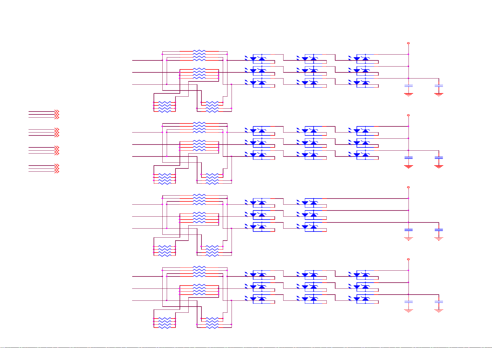
9-12-2 Ambilight 11-LED
PWM2-R1 2
PWM2-G1 2
PWM2-B1 2
PWM2-R2 2
PWM2-G2 2
PWM2-B2 2
PWM2-R3 2
PWM2-G3 2
PWM2-B3 2
PWM2-R4 2
PWM2-G4 2
PWM2-B4 2
PWM2-B1
PWM2-R1
PWM2-G1
PWM2-B2
PWM2-R2
PWM2-G2
PWM2-B3
PWM2-R3
PWM2-G3
PWM2-B4
PWM2-R4
PWM2-G4
R021 560R
R022 560R
R023 560R
R024 560R
R025 560R
R026 560R
R027 560R
R028 560R
R029 560R
R030 560R
R031 560R
R032 560R
R033 560R
R034 560R
R035 560R
R036 560R
1
2
3
4
R020 NC/ 560R
1
2
3
4
1
2
3
4
R018 NC/ 560R
1
2
3
4
1
2
3
4
R016 NC/ 560R
1
2
3
4
1
2
3
4
R015 NC/ 560R
1
2
3
4
8
7
6
5
8
7
6
5
R040 22R 1/16W 5%
R041 22R 1/16W 5%
R042 22R 1/16W 5%
R043 22R 1/16W 5%
NC/22R
R017
8
7
6
5
8
7
6
5
R060 22R 1/16W 5%
R061 22R 1/16W 5%
R062 22R 1/16W 5%
R063 22R 1/16W 5%
NC/180R
R014
8
7
6
5
8
7
6
5
R064 180R
R065 180R
R066 180R
R067 180R
NC/22R
R013
8
7
6
5
8
7
6
5
R044 22R 1/16W 5%
R045 22R 1/16W 5%
R046 22R 1/16W 5%
R047 22R 1/16W 5%
NC/22R
R019
D009
6
5
4
Red BlueGreen
3
2
1
P5018/RSSGBB7-2K14
D006
6
5
4
Red BlueGreen
3
2
1
P5018/RSSGBB7-2K14
D004
6
5
4
Red BlueGreen
3
2
1
P5018/RSSGBB7-2K14
D001
6
5
4
Red BlueGreen
3
2
1
P5018/RSSGBB7-2K14
D010
6
5
4
Red BlueGreen
3
2
1
P5018/RSSGBB7-2K14
D007
6
5
4
Red BlueGreen
3
2
1
P5018/RSSGBB7-2K14
D005
6
5
4
Red BlueGreen
3
2
1
P5018/RSSGBB7-2K14
D002
6
5
4
Red BlueGreen
3
2
1
P5018/RSSGBB7-2K14
D011
6
5
4
Red BlueGreen
3
2
1
P5018/RSSGBB7-2K14
D008
6
5
4
Red BlueGreen
3
2
1
P5018/RSSGBB7-2K14
D003
6
5
4
Red BlueGreen
3
2
1
P5018/RSSGBB7-2K14
+12V
+12V
+12V
+12V
C012
100N16V
C014
100N16V
C010
100N16V
C008
100N16V
C013
NC/100N F 50V
C015
NC/100N F 50V
C011
NC/100N F 50V
C009
NC/100N F 50V

10. Styling Sheets
0040
0030
1056
1184
1053
1054
1050
50R
63
36 1184
1057
50L
10.1 6504 series 50”
WIFI02
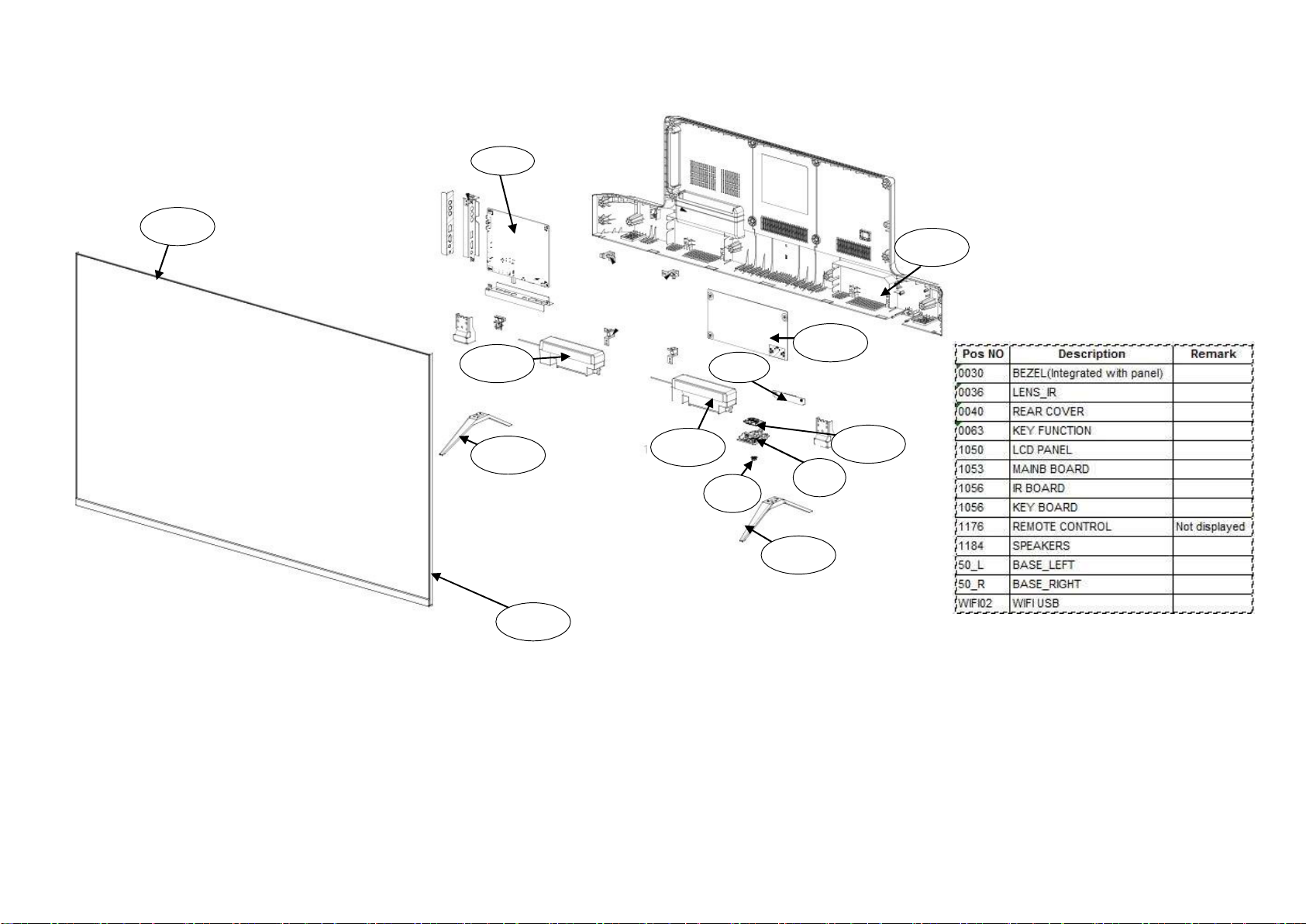
10.2 6654 series 50”/55”
0040
0030
1056
1184
1053
1054
1050
50R
36
63
1184
50L
WIFI02

10.3 6654 series 58”/65”
0030
1056
1053
1054
1050
50R 36
63
1184
50L
1184
0040
WIFI02

10.4 6794 series 55”
1056
1184
1053
1054
1050
36 1061
30B
0040
50L
1061
50R 63
30T
1062
WIFI02

10.5 6794 series 65”
0040
30T
50L
1056
1184
1053
1054
1050
50R
36
63
1061
1061
1063
1062
30B
WIFI02
 Loading...