

Page 1
Colour Television Chassis
QM16.1L
LA
Contents Page Contents Page
1. Revision List 2
2. Technical Specs, Diversity, and Connections 2
3. Precautions, Notes, and Abbreviation List 5
4. Mechanical Instructions 9
Cable dressing (50" 6601 series) 9
Cable dressing (55" 6601 series) 10
5. Service Modes, Error Codes, and Fault Finding 14
6. Alignments 22
7. Circuit Descriptions 24
8. IC Data Sheets 31
9. Block Diagrams
Block diagram series 35
10. Circuit Diagrams and PWB Layouts Drawing PWB
A 715G7374 PSU
A 715G6973 PSU 42 46-47
B 715G7049 SSB 48 63-64
J 715G7074 IR/LED Panel 65 66
E 715G7088 Keyboard control panel 67 68
11. Styling Sheets
6601 series 50" 69
6601 series 55" 70
36 40-41
Published by CQZ/SC 1627 Quality Printed in the Netherlands Subject to modification EN 3122 785 20160
2016-Jul-08
2016 ©
TP Vision Netherlands B.V.
All rights reserved. Specifications are subject to change without notice. Trademarks are the
property of Koninklijke Philips Electronics N.V. or their respective owners.
TP Vision Netherlands B.V. reserves the right to change products at any time without being obliged to adjust
earlier supplies accordingly.
PHILIPS and the PHILIPS’ Shield Emblem are used under license from Koninklijke Phili ps Electronics N.V.
Page 2
EN 2 QM16.1L LA1.
Revision List
1. Revision List
Manual xxxx xxx xxxx.0
• First release.
2. Technical Specs, Diversity, and Connections
Index of this chapter:
• Specifications are indicative (subject to change).
2.1 Technical Specifications
2.2 Directions for Use
2.3 Connections
2.4 Chassis Overview
2.1 Technical Specifications
For on-line product support please use the links in back to
div.table 2-1. Here is product information available, as well as
getting started, user manuals, frequently asked questions and
Notes:
software & drivers.
• Figures can deviate due to the different set executions.
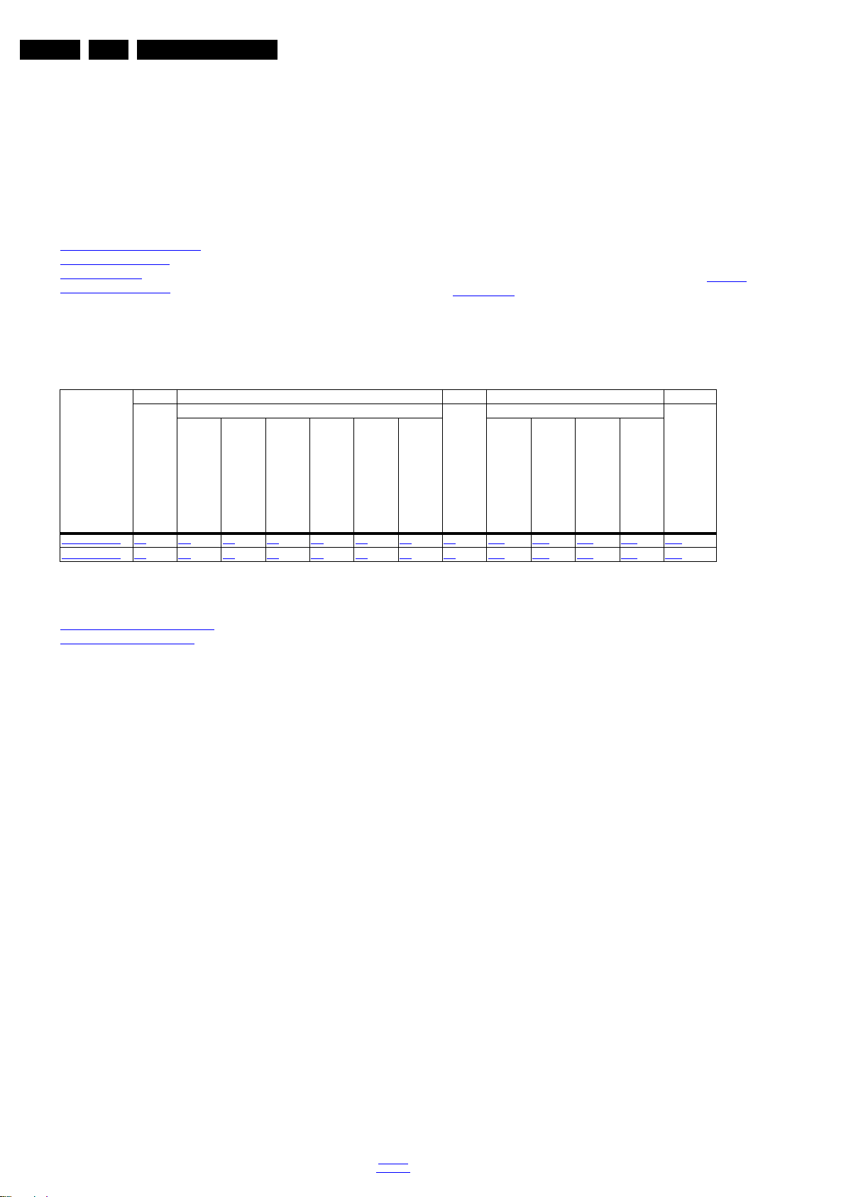
Table 2-1 Described Model Numbers and Diversity
24 910 11
CTN
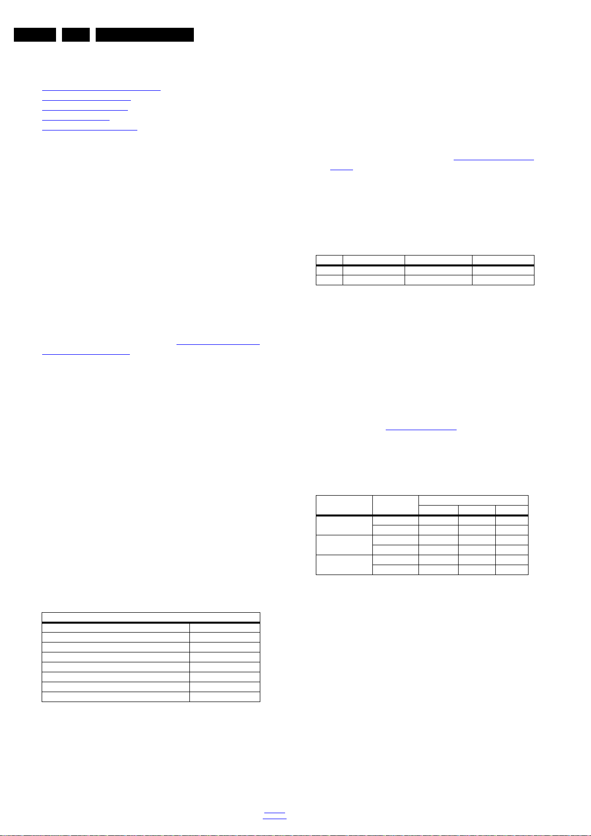
50PUG6601/77 2-1 4-1 4-3 4-4 4-5 4-6 4-7 9.1 10.1 10.3 10.4 10.5 11.1
55PUG6601/77 2-1 4-2 4-3 4-4 4-5 4-6 4-7 9.1 10.2 10.3 10.4 10.5 11.2
Mechanics
Connection Overview
Wire Dressing
Stand Removal
Schematics
Rear Cover Removal
Kyboard Control Removal
SSB Removal
IR/LED Board Removal
Block Diagram
Power Supply
SSB
2.2 Directions for Use
Directions for use can be downloaded from the following
websites:
http://www.philips.com/support
http://www.p4c.philips.com
J (IR/LED)
E (Keyboard/Leading Edge)
Styling
2016-Jul-08
back to
div.table
Page 3
2.3 Connections
TV ANTENNA
SERV.U
AUDIO IN
DVI
HDMI 3
ARC
SPDIF
OUT
NETWORK
HDMI 2
ARC
USB3
USB
USB
HDMI
ARC/MHL
1
2
1
CVBS
R
L
20160_001.eps
1
2
6
9
12
Side Connectors
Rear Connectors
7
3
8
10
13
11
4
5
1 2 3 4
10000_022_090121.eps
090121
1 2 3 4
10000_022_090121.eps
090121
10000_017_090121.eps
090428
19
1
18 2
Technical Specs, Diversity, and Connections
EN 3QM16.1L LA 2.
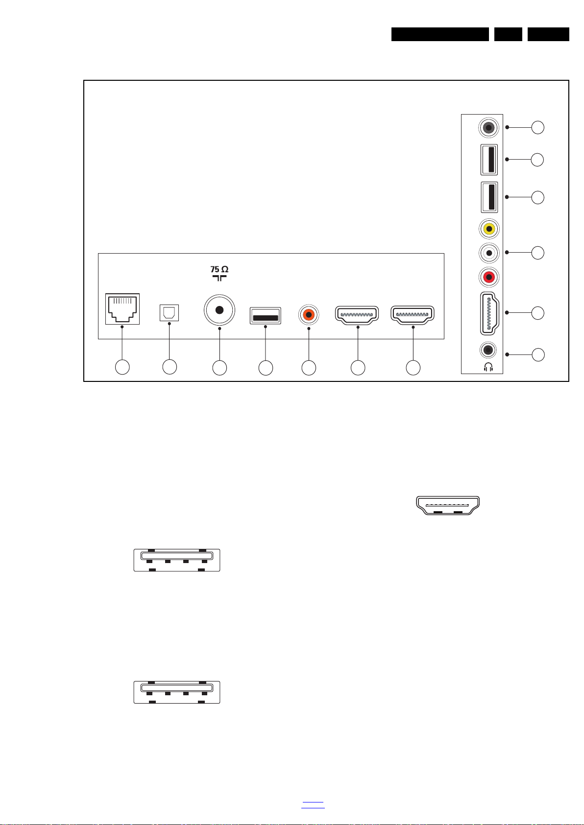
2.3.1 Side Connections
Figure 2-1 Connection overview
Note: The following connector colour abbreviations are used
(acc. to DIN/IEC 757): Bk= Black, Bu= Blue, Gn= Green,
Gy= Grey, Rd= Red, Wh= White, Ye= Yellow.
1 - Service / UART
1 - Ground Gnd H
2 - UART_TX Transmit k
3 - UART_RX Receive j
2 - USB1
Figure 2-2 USB (type A)
1-+5V k
2 - Data (-) jk
3 - Data (+) jk
4 - Ground Gnd H
3 - USB2
Figure 2-3 USB (type A)
1-+5V k
2 - Data (-) jk
3 - Data (+) jk
4 - Ground Gnd H
back to
div.table
4 - EXT: Video CVBS - In, Audio - In
Ye -Video - CBVS 1 V
Wh -Audio - L 0.5 V
Rd -Audio - R 0.5 V
5 - HDMI 1: Digital Video - In, Digital Audio with ARC/MHL In/Out
Figure 2-4 HDMI (type A) connector
1 - D2+ Data channel j
2 - Shield Gnd H
3 - D2- Data channel j
4 - D1+ Data channel j
5 - Shield Gnd H
6 - D1- Data channel j
7 - D0+ Data channel j
8 - Shield Gnd H
9 - D0- Data channel j
10 - CLK+ Data channel j
11 - Shield Gnd H
12 - CLK- Data channel j
13 - Easylink/CEC Control channel jk
14 - ARC Audio Return Channel k
15 - DDC_SCL DDC clock j
16 - DDC_SDA DDC data jk
17 - Ground Gnd H
18 - +5V j
19 - HPD Hot Plug Detect j
20 - Ground Gnd H
6- Head phone (Output)
Bk -Head phone 80 - 600 / 10 mW ot
/ 75 W jq
PP
/ 10 kW jq
RMS
/ 10 kW jq
RMS
2016-Jul-08
Page 4
EN 4 QM16.1L LA2.
10000_025_090121.eps
120320
1 2 3 4
10000_022_090121.eps
090121
10000_017_090121.eps
090428
19
1
18 2
10000_017_090121.eps
090428
19
1
18 2
Technical Specs, Diversity, and Connections
2.3.2 Rear Connections
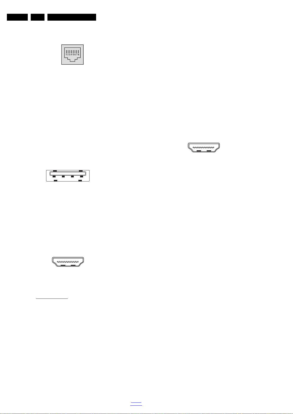
7 - RJ45: Ethernet
Figure 2-5 Ethernet connector
1 - TD+ Transmit signal k
2 - TD- Transmit signal k
3 - RD+ Receive signal j
4 - CT Centre Tap: DC level fixation
5 - CT Centre Tap: DC level fixation
6 - RD- Receive signal j
7 - GND Gnd H
8 - GND Gnd H
8 - Cinch: Digital Audio - Out
BK - Coaxial 0.4 - 0.6V
/ 75 W kq
PP
9- TV ANTENNA - In
Signal input from an antenna, cable or satellite.
10 - USB3
1 - D2+ Data channel j
2 - Shield Gnd H
3 - D2- Data channel j
4 - D1+ Data channel j
5 - Shield Gnd H
6 - D1- Data channel j
7 - D0+ Data channel j
8 - Shield Gnd H
9 - D0- Data channel j
10 - CLK+ Data channel j
11 - Shield Gnd H
12 - CLK- Data channel j
13 - Easylink/CEC Control channel jk
14 - ARC Audio Return Channel k
15 - DDC_SCL DDC clock j
16 - DDC_SDA DDC data jk
17 - Ground Gnd H
18 - +5V j
19 - HPD Hot Plug Detect j
20 - Ground Gnd H
13- HDMI 2: Digital Video - In, Digital Audio with ARC In/Out
Figure 2-8 HDMI (type A) connector
Figure 2-6 USB (type A)
1-+5V k
2 - Data (-) jk
3 - Data (+) jk
4 - Ground Gnd H
11 - Audio - In: Left / Right, DVI
Gn - Audio L/R in 0.5 V
/ 10 k jq
RMS
12- HDMI 3: Digital Video - In, Digital Audio with ARC In/Out
Figure 2-7 HDMI (type A) connector
2.4 Chassis Overview
Refer to 9. Block Diagrams for PWB/CBA locations.
1 - D2+ Data channel j
2 - Shield Gnd H
3 - D2- Data channel j
4 - D1+ Data channel j
5 - Shield Gnd H
6 - D1- Data channel j
7 - D0+ Data channel j
8 - Shield Gnd H
9 - D0- Data channel j
10 - CLK+ Data channel j
11 - Shield Gnd H
12 - CLK- Data channel j
13 - Easylink/CEC Control channel jk
14 - ARC Audio Return Channel k
15 - DDC_SCL DDC clock j
16 - DDC_SDA DDC data jk
17 - Ground Gnd H
18 - +5V j
19 - HPD Hot Plug Detect j
20 - Ground Gnd H
2016-Jul-08
back to
div.table
Page 5

Precautions, Notes, and Abbreviation List
3. Precautions, Notes, and Abbreviation List
Index of this chapter:
3.1 Safety Instructions
3.2 Warnings
3.3 Notes
3.4 Abbreviation List
3.1 Safety Instructions
Safety regulations require the following during a repair:
• Connect the set to the Mains/AC Power via an isolation
transformer (> 800 VA).
• Replace safety components, indicated by the symbol h,
only by components identical to the original ones. Any
other component substitution (other than original type) may
increase risk of fire or electrical shock hazard.
Safety regulations require that after a repair, the set must be
returned in its original condition. Pay in particular attention to
the following points:
• Route the wire trees correctly and fix them with the
mounted cable clamps.
• Check the insulation of the Mains/AC Power lead for
external damage.
• Check the strain relief of the Mains/AC Power cord for
proper function.
• Check the electrical DC resistance between the Mains/AC
Power plug and the secondary side (only for sets that have
a Mains/AC Power isolated power supply):
1. Unplug the Mains/AC Power cord and connect a wire
between the two pins of the Mains/AC Power plug.
2. Set the Mains/AC Power switch to the “on” position
(keep the Mains/AC Power cord unplugged!).
3. Measure the resistance value between the pins of the
Mains/AC Power plug and the metal shielding of the
tuner or the aerial connection on the set. The reading
should be between 4.5 M and 12 M.
4. Switch “off” the set, and remove the wire between the
two pins of the Mains/AC Power plug.
• Check the cabinet for defects, to prevent touching of any
inner parts by the customer.
3.2 Warnings
• All ICs and many other semiconductors are susceptible to
electrostatic discharges (ESD w). Careless handling
during repair can reduce life drastically. Make sure that,
during repair, you are connected with the same potential as
the mass of the set by a wristband with resistance. Keep
components and tools also at this same potential.
• Be careful during measurements in the high voltage
section.
• Never replace modules or other components while the unit
is switched “on”.
• When you align the set, use plastic rather than metal tools.
This will prevent any short circuits and the danger of a
circuit becoming unstable.
3.3 Notes
3.3.1 General
• Measure the voltages and waveforms with regard to the
chassis (= tuner) ground (H), or hot ground (I), depending
on the tested area of circuitry. The voltages and waveforms
shown in the diagrams are indicative. Measure them in the
Service Default Mode with a colour bar signal and stereo
sound (L: 3 kHz, R: 1 kHz unless stated otherwise) and
picture carrier at 475.25 MHz for PAL, or 61.25 MHz for
NTSC (channel 3).
• Where necessary, measure the waveforms and voltages
with (D) and without (E) aerial signal. Measure the
voltages in the power supply section both in normal
operation (G) and in stand-by (F). These values are
indicated by means of the appropriate symbols.
3.3.2 Schematic Notes
• All resistor values are in ohms, and the value multiplier is
often used to indicate the decimal point location (e.g. 2K2
indicates 2.2 k).
• Resistor values with no multiplier may be indicated with
either an “E” or an “R” (e.g. 220E or 220R indicates 220 ).
• All capacitor values are given in micro-farads (10
nano-farads (n 10
• Capacitor values may also use the value multiplier as the
decimal point indication (e.g. 2p2 indicates 2.2 pF).
• An “asterisk” (*) indicates component usage varies. Refer
to the diversity tables for the correct values.
• The correct component values are listed on the Philips
Spare Parts Web Portal.
3.3.3 Spare Parts
For the latest spare part overview, consult your Philips Spare
Part web portal.
3.3.4 BGA (Ball Grid Array) ICs
Introduction
For more information on how to handle BGA devices, visit this
URL: http://www.atyourservice-magazine.com
“Magazine”, then go to “Repair downloads”. Here you will find
Information on how to deal with BGA-ICs.
BGA Temperature Profiles
For BGA-ICs, you must use the correct temperature-profile.
Where applicable and available, this profile is added to the IC
Data Sheet information section in this manual.
3.3.5 Lead-free Soldering
Due to lead-free technology some rules have to be respected
by the workshop during a repair:
• Use only lead-free soldering tin. If lead-free solder paste is
required, please contact the manufacturer of your soldering
equipment. In general, use of solder paste within
workshops should be avoided because paste is not easy to
store and to handle.
• Use only adequate solder tools applicable for lead-free
soldering tin. The solder tool must be able:
– To reach a solder-tip temperature of at least 400°C.
– To stabilize the adjusted temperature at the solder-tip.
– To exchange solder-tips for different applications.
• Adjust your solder tool so that a temperature of around
360°C - 380°C is reached and stabilized at the solder joint.
Heating time of the solder-joint should not exceed ~ 4 sec.
Avoid temperatures above 400°C, otherwise wear-out of
tips will increase drastically and flux-fluid will be destroyed.
To avoid wear-out of tips, switch “off” unused equipment or
reduce heat.
• Mix of lead-free soldering tin/parts with leaded soldering
tin/parts is possible but PHILIPS recommends strongly to
avoid mixed regimes. If this cannot be avoided, carefully
clear the solder-joint from old tin and re-solder with new tin.
3.3.6 Alternative BOM identification
It should be noted that on the European Service website,
“Alternative BOM” is referred to as “Design variant”.
The third digit in the serial number (example:
AG2B0335000001) indicates the number of the alternative
B.O.M. (Bill Of Materials) that has been used for producing the
specific TV set. In general, it is possible that the same TV
model on the market is produced with e.g. two different types
of displays, coming from two different suppliers. This will then
back to
div.table
-9
), or pico-farads (p 10
. Select
EN 5QM16.1L LA 3.
-6
),
-12
).
2016-Jul-08
Page 6
EN 6 QM16.1L LA3.
10000_053_110228.eps
110228
Precautions, Notes, and Abbreviation List
result in sets which have the same CTN (Commercial Type
Number; e.g. 28PW9515/12) but which have a different B.O.M.
number.
By looking at the third digit of the serial number, one can
identify which B.O.M. is used for the TV set he is working with.
If the third digit of the serial number contains the number “1”
(example: AG1B033500001), then the TV set has been
manufactured according to B.O.M. number 1. If the third digit is
a “2” (example: AG2B0335000001), then the set has been
produced according to B.O.M. no. 2. This is important for
ordering the correct spare parts!
For the third digit, the numbers 1...9 and the characters A...Z
can be used, so in total: 9 plus 26= 35 different B.O.M.s can be
indicated by the third digit of the serial number.
Identification: The bottom line of a type plate gives a 14-digit
serial number. Digits 1 and 2 refer to the production centre (e.g.
SN is Lysomice, RJ is Kobierzyce), digit 3 refers to the B.O.M.
code, digit 4 refers to the Service version change code, digits 5
and 6 refer to the production year, and digits 7 and 8 refer to
production week (in example below it is 2010 week 10 / 2010
week 17). The 6 last digits contain the serial number.
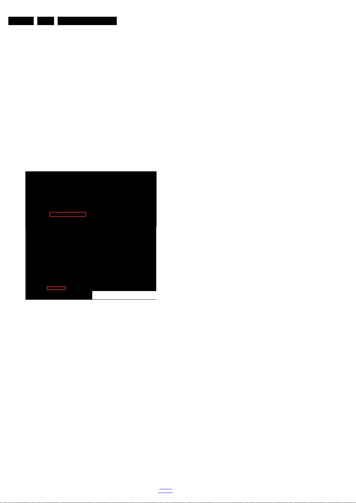
Figure 3-1 Serial number (example)
3.3.7 Board Level Repair (BLR) or Component Level Repair (CLR)
If a board is defective, consult your repair procedure to decide
if the board has to be exchanged or if it should be repaired on
component level.
If your repair procedure says the board should be exchanged
completely, do not solder on the defective board. Otherwise, it
cannot be returned to the O.E.M. supplier for back charging!
3.3.8 Practical Service Precautions
• It makes sense to avoid exposure to electrical shock.
While some sources are expected to have a possible
dangerous impact, others of quite high potential are of
limited current and are sometimes held in less regard.
• Always respect voltages. While some may not be
dangerous in themselves, they can cause unexpected
reactions that are best avoided. Before reaching into a
powered TV set, it is best to test the high voltage insulation.
It is easy to do, and is a good service precaution.
3.4 Abbreviation List
0/6/12 SCART switch control signal on A/V
board. 0 = loop through (AUX to TV),
6 = play 16 : 9 format, 12 = play 4 : 3
format
AARA Automatic Aspect Ratio Adaptation:
algorithm that adapts aspect ratio to
remove horizontal black bars; keeps
the original aspect ratio
ACI Automatic Channel Installation:
algorithm that installs TV channels
directly from a cable network by
means of a predefined TXT page
ADC Analogue to Digital Converter
AFC Automatic Frequency Control: control
signal used to tune to the correct
frequency
AGC Automatic Gain Control: algorithm that
controls the video input of the feature
box
AM Amplitude Modulation
AP Asia Pacific
AR Aspect Ratio: 4 by 3 or 16 by 9
ASF Auto Screen Fit: algorithm that adapts
aspect ratio to remove horizontal black
bars without discarding video
information
ATSC Advanced Television Systems
Committee, the digital TV standard in
the USA
ATV See Auto TV
Auto TV A hardware and software control
system that measures picture content,
and adapts image parameters in a
dynamic way
AV External Audio Video
AVC Audio Video Controller
AVIP Audio Video Input Processor
B/G Monochrome TV system. Sound
carrier distance is 5.5 MHz
BDS Business Display Solutions (iTV)
BLR Board-Level Repair
BTSC Broadcast Television Standard
Committee. Multiplex FM stereo sound
system, originating from the USA and
used e.g. in LATAM and AP-NTSC
countries
B-TXT Blue TeleteXT
C Centre channel (audio)
CEC Consumer Electronics Control bus:
remote control bus on HDMI
connections
CL Constant Level: audio output to
connect with an external amplifier
CLR Component Level Repair
ComPair Computer aided rePair
CP Connected Planet / Copy Protection
CSM Customer Service Mode
CTI Color Transient Improvement:
manipulates steepness of chroma
transients
CVBS Composite Video Blanking and
Synchronization
DAC Digital to Analogue Converter
DBE Dynamic Bass Enhancement: extra
low frequency amplification
DCM Data Communication Module. Also
referred to as System Card or
Smartcard (for iTV).
DDC See “E-DDC”
D/K Monochrome TV system. Sound
carrier distance is 6.5 MHz
DFI Dynamic Frame Insertion
DFU Directions For Use: owner's manual
DMR Digital Media Reader: card reader
DMSD Digital Multi Standard Decoding
DNM Digital Natural Motion
2016-Jul-08
back to
div.table
Page 7

Precautions, Notes, and Abbreviation List
EN 7QM16.1L LA 3.
DNR Digital Noise Reduction: noise
reduction feature of the set
DRAM Dynamic RAM
DRM Digital Rights Management
DSP Digital Signal Processing
DST Dealer Service Tool: special remote
control designed for service
technicians
DTCP Digital Transmission Content
Protection; A protocol for protecting
digital audio/video content that is
traversing a high speed serial bus,
such as IEEE-1394
DVB-C Digital Video Broadcast - Cable
DVB-T Digital Video Broadcast - Terrestrial
DVD Digital Versatile Disc
DVI(-d) Digital Visual Interface (d= digital only)
E-DDC Enhanced Display Data Channel
(VESA standard for communication
channel and display). Using E-DDC,
the video source can read the EDID
information form the display.
EDID Extended Display Identification Data
(VESA standard)
EEPROM Electrically Erasable and
Programmable Read Only Memory
EMI Electro Magnetic Interference
EPG Electronic Program Guide
EPLD Erasable Programmable Logic Device
EU Europe
EXT EXTernal (source), entering the set by
SCART or by cinches (jacks)
FDS Full Dual Screen (same as FDW)
FDW Full Dual Window (same as FDS)
FLASH FLASH memory
FM Field Memory or Frequency
Modulation
FPGA Field-Programmable Gate Array
FTV Flat TeleVision
Gb/s Giga bits per second
G-TXT Green TeleteXT
H H_sync to the module
HD High Definition
HDD Hard Disk Drive
HDCP High-bandwidth Digital Content
Protection: A “key” encoded into the
HDMI/DVI signal that prevents video
data piracy. If a source is HDCP coded
and connected via HDMI/DVI without
the proper HDCP decoding, the
picture is put into a “snow vision” mode
or changed to a low resolution. For
normal content distribution the source
and the display device must be
enabled for HDCP “software key”
decoding.
HDMI High Definition Multimedia Interface
HP HeadPhone
I Monochrome TV system. Sound
2
C Inter IC bus
I
2
I
D Inter IC Data bus
2
S Inter IC Sound bus
I
carrier distance is 6.0 MHz
IF Intermediate F requency
IR Infra Red
IRQ Interrupt Request
ITU-656 The ITU Radio communication Sector
(ITU-R) is a standards body
subcommittee of the International
Telecommunication Union relating to
radio communication. ITU-656 (a.k.a.
SDI), is a digitized video format used
for broadcast grade video.
Uncompressed digital component or
digital composite signals can be used.
back to
div.table
The SDI signal is self-synchronizing,
uses 8 bit or 10 bit data words, and has
a maximum data rate of 270 Mbit/s,
with a minimum bandwidth of 135
MHz.
iTV Institutional TeleVision; TV sets for
hotels, hospitals etc.
LS Last Status; The settings last chosen
by the customer and read and stored
in RAM or in the NVM. They are called
at start-up of the set to configure it
according to the customer's
preferences
LATAM Latin America
LCD Liquid Crystal Display
LED Light Emitting Diode
L/L' Monochrome TV system. Sound
carrier distance is 6.5 MHz. L' is Band
I, L is all bands except for Band I
LPL LG.Philips LCD (supplier)
LS Loudspeaker
LVDS Low Voltage Differential Signalling
Mbps Mega bits per second
M/N Monochrome TV system. Sound
carrier distance is 4.5 MHz
MHEG Part of a set of international standards
related to the presentation of
multimedia information, standardised
by the Multimedia and Hypermedia
Experts Group. It is commonly used as
a language to describe interactive
television services
MIPS Microprocessor without Interlocked
Pipeline-Stages; A RISC-based
microprocessor
MOP Matrix Output Processor
MOSFET Metal Oxide Silicon Field Effect
Transistor, switching device
MPEG Motion Pictures Experts Group
MPIF Multi Platform InterFace
MUTE MUTE Line
MTV Mainstream TV: TV-mode with
Consumer TV features enabled (iTV)
NC Not Connected
NICAM Near Instantaneous Compounded
Audio Multiplexing. This is a digital
sound system, mainly used in Europe.
NTC Negative Temperature Coefficient,
non-linear resistor
NTSC National Television Standard
Committee. Color system mainly used
in North America and Japan. Color
carrier NTSC M/N= 3.579545 MHz,
NTSC 4.43= 4.433619 MHz (this is a
VCR norm, it is not transmitted off-air)
NVM Non-Volatile Memory: IC containing
TV related data such as alignments
O/C Open Circuit
OSD On Screen Display
OAD Over the Air Download. Method of
software upgrade via RF transmission.
Upgrade software is broadcasted in
TS with TV channels.
OTC On screen display Teletext and
Control; also called Artistic (SAA5800)
P50 Project 50: communication protocol
between TV and peripherals
PAL Phase Alternating Line. Color system
mainly used in West Europe (colour
carrier = 4.433619 MHz) and South
America (colour carrier
PAL M = 3.575612 MHz and
PAL N = 3.582056 MHz)
PCB Printed Circuit Board (same as “PWB”)
PCM Pulse Code Modulation
2016-Jul-08
Page 8

EN 8 QM16.1L LA3.
Precautions, Notes, and Abbreviation List
PDP Plasma Display Panel
PFC Power Factor Corrector (or
Pre-conditioner)
PIP Picture In Picture
PLL Phase Locked Loop. Used for e.g.
FST tuning systems. The customer
can give directly the desired frequency
POD Point Of Deployment: a removable
CAM module, implementing the CA
system for a host (e.g. a TV-set)
POR Power On Reset, signal to reset the uP
PSDL Power Supply for Direct view LED
backlight with 2D-dimming
PSL Power Supply with integrated LED
drivers
PSLS Power Supply with integrated LED
drivers with added Scanning
functionality
PTC Positive Temperature Coefficient,
non-linear resistor
PWB Printed Wiring Board (same as “PCB”)
PWM Pulse Width Modulation
QRC Quasi Resonant Converter
QTNR Quality Temporal Noise Reduction
QVCP Quality Video Composition Processor
RAM Random Access Memory
RGB Red, Green, and Blue. The primary
color signals for TV. By mixing levels
of R, G, and B, all colors (Y/C) are
reproduced.
RC Remote Control
RC5 / RC6 Signal protocol from the remote
control receiver
RESET RESET signal
ROM Read Only Memory
RSDS Reduced Swing Differential Signalling
data interface
R-TXT Red TeleteXT
SAM Service Alignment Mode
S/C Short Circuit
SCART Syndicat des Constructeurs
d'Appareils Radiorécepteurs et
SCL Serial Clock I
Téléviseurs
SCL-F CLock Signal on Fast I
SD Standard Definition
SDA Serial Data I
SDA-F DAta Signal on Fast I
2
C
2
C bus
2
C
2
C bus
SDI Serial Digital Interface, see “ITU-656”
SDRAM Synchronous DRAM
SECAM SEequence Couleur Avec Mémoire.
Colour system mainly used in France
and East Europe. Colour
carriers = 4.406250 MHz and
4.250000 MHz
SIF Sound Intermediate Frequency
SMPS Switched Mode Power Supply
SoC System on Chip
SOG Sync On Green
SOPS Self Oscillating Power Supply
SPI Serial Peripheral Interface bus; a
4-wire synchronous serial data link
standard
S/PDIF Sony Philips Digital InterFace
SRAM Static RAM
SRP Service Reference Protocol
SSB Small Signal Board
SSC Spread Spectrum Clocking, used to
reduce the effects of EMI
STB Set Top Box
STBY STand-BY
SVGA 800 × 600 (4:3)
SVHS Super Video Home System
SW Software
SWAN Spatial temporal Weighted Averaging
Noise reduction
SXGA 1280 × 1024
TFT Thin Film Transistor
THD Total Harmonic Distortion
TMDS Transmission Minimized Differential
Signalling
TS Transport Stream
TXT TeleteXT
TXT-DW Dual Window with TeleteXT
UI User Interface
uP Microprocessor
UXGA 1600 × 1200 (4:3)
V V-sync to the module
VESA Video Electronics Standards
Association
VGA 640 × 480 (4:3)
VL Variable Level out: processed audio
output toward external amplifier
VSB Vestigial Side Band; modulation
method
WYSIWYR What You See Is What You Record:
record selection that follows main
picture and sound
WXGA 1280 × 768 (15:9)
XTAL Quartz crystal
XGA 1024 × 768 (4:3)
Y Luminance signal
Y/C Luminance (Y) and Chrominance (C)
signal
YPbPr Component video. Luminance and
scaled color difference signals (B-Y
and R-Y)
YUV Component video
2016-Jul-08
back to
div.table
Page 9
4. Mechanical Instructions
20160_100.eps
CN408
CN700
CN401
CN6005
CN8601
CN9103
CN4250
MAIN POWER SUPPLY
(1054)
A
SSB
(1053)
B
ECN700
ECN6005
ECN408
ECN401
ECN401
ECN6005
LOUDSPEAKER
(1184)
LOUDSPEAKER
(1184)
ECN4250
IR/LED BOARD
(1056)
J
KEYBOARD CONTROL
(1057)
E
CN01
WIFI Module
(WiFi01)
Index of this chapter:
4.1 Cable Dressing
4.2 Service Positions
4.3 Assembly/Panel Removal
4.4 Set Re-assembly
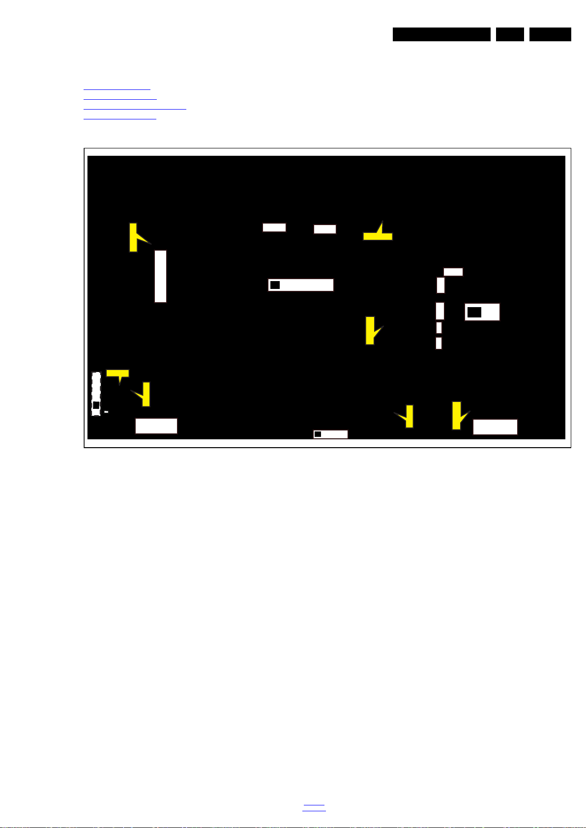
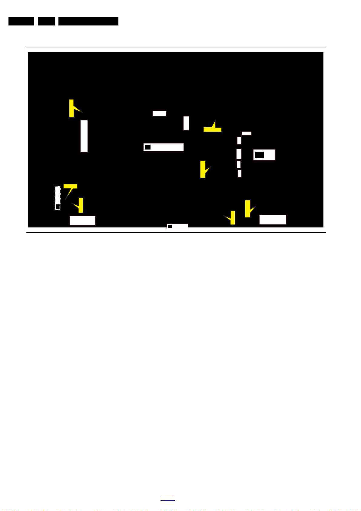
4.1 Cable Dressing
Mechanical Instructions
Notes:
• Figures below can deviate slightly from the actual situation,
due to the different set executions.
EN 9QM16.1L LA 4.
Figure 4-1 Cable dressing (50" 6601 series)
back to
div.table
2016-Jul-08
Page 10
EN 10 QM16.1L LA4.
20160_101.eps
CN408
CN700
CN401
CN6005
CN8101
CN9101
CN4250
MAIN POWER SUPPLY
(1054)
A
SSB
(1053)
B
ECN700
ECN6005
ECN408
ECN401
ECN401
ECN6005
LOUDSPEAKER
(1184)
LOUDSPEAKER
(1184)
ECN4250
IR/LED BOARD
(1056)
J
KEYBOARD CONTROL
(1057)
E
WIFI Module
(WiFi01)
Mechanical Instructions
Figure 4-2 Cable dressing (55" 6601 series)
4.2 Se rvice Positions
For easy servicing of a TV set, the set should be put face down
on a soft flat surface, foam buffers or other specific workshop
tools. Ensure that a stable situation is created to perform
measurements and alignments. When using foam bars take
care that these always support the cabinet and never only the
display. Caution: Failure to follow these guidelines can
seriously damage the display!
Ensure that ESD safe measures are taken.
2016-Jul-08
back to
div.table
Page 11
Mechanical Instructions
EN 11QM16.1L LA 4.
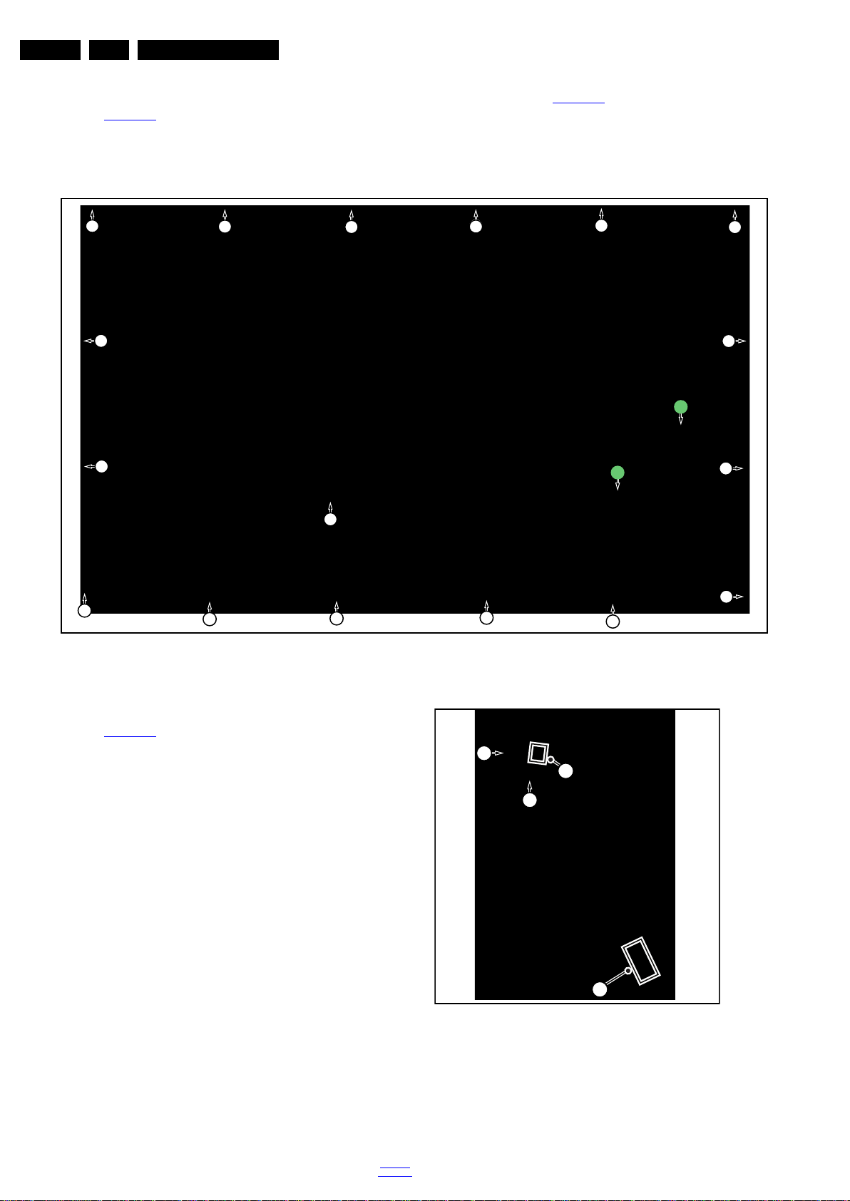
4.3 Assembly/Panel Removal
Instructions below apply to the 50PUG6601/77, but will be
similar for other 50"/55"PUG6601 series models.
1
1
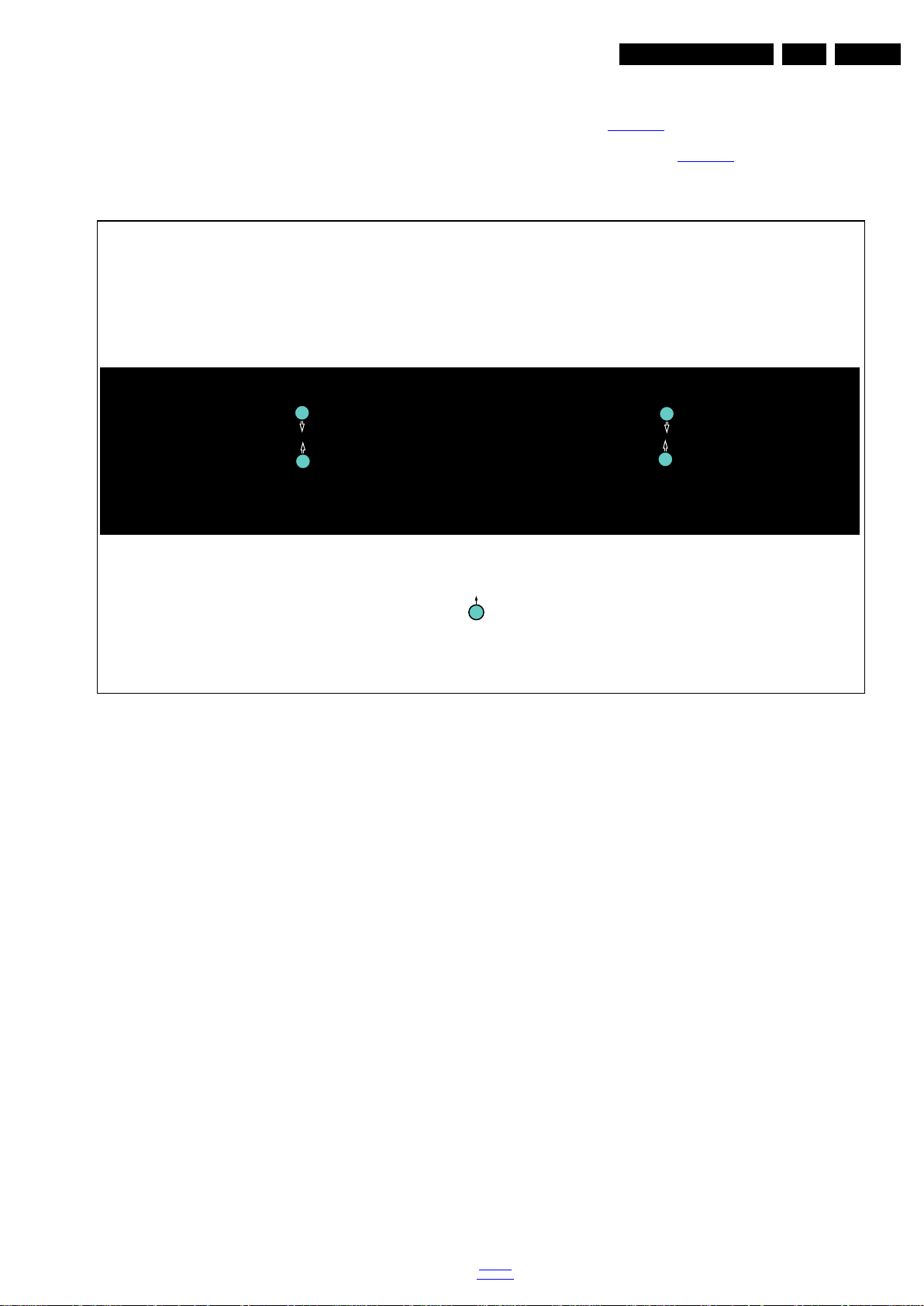
4.3.1 Stand
Refer to Figure 4-3
1. Remove the fixation screws [1] that secure the stand
bracket. Refer to Figure 4-3
2. Take the stand bracket out from the set.
for details.
for details.
1
1
M4 × 16
1
Figure 4-3 Stand removal
20160_102.eps
back to
div.table
2016-Jul-08
Page 12
EN 12 QM16.1L LA4.
20160_103.eps
2
2
2
2
2
2
2
2
2
2
2
2
2
2
2
2
2
3
3
20160_104.eps
2
2
1
3
Mechanical Instructions
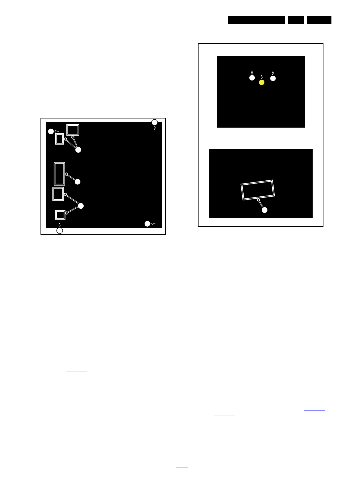
4.3.2 Rear Cover
Refer to Figure 4-4
Warning: The Keyboard catch on the Back cover, disconnect
the Keyboard cord before removing the rear cover.
for details.
1. Remove the fixation screws [2] and [3] that secure the rear
cover. Refer to Figure 4-4
2. Gently lift the rear cover from the TV. Make sure that wires
and cables are not damaged while lifting the rear cover
from the set.
for details.
4.3.3 Keyboard Control unit
Refer to Figure 4-5
1. The Keyboard catch on the Back cover, so the cable
connector[1] form the SSB must be released first before
opening of Back cover.
2. Remove all the fixation screws from the keyboard [2].Then
Unplug the connector[3] from the keyboard control panel.
When defective, replace the whole unit.
for details.
Figure 4-4 Rear cover removal
Figure 4-5 Keyboard removal
2016-Jul-08
back to
div.table
Page 13
4.3.4 Small Signal Board (SSB)
20160_105.eps
2
1
3
3
3
3
2
20160_106.eps
3
Step 1
Step 2
1
1
2
Mechanical Instructions
EN 13QM16.1L LA 4.
Refer to Figure 4-6
Caution: it is mandatory to remount all different screws at their
original position during re-assembly. Failure to do so may result
in damaging the SSB.
1. Release the clips from the LVDS connector that connect
with the SSB[1].
Caution: be careful, as these are very fragile connectors!
2. Unplug all other connectors [2].
3. Remove all the fixation screws from the SSB [3].
4. The SSB can now be shifted from side connector cover,
then lifted and taken out of the I/O bracket. Refer to
Figure 4-6
for details.
for details.
Figure 4-6 SSB removal
4.3.5 Power Supply Unit (PSU)
Caution: it is mandatory to remount all different screws at their
original position during re-assembly. Failure to do so may result
in damaging the PSU.
1. Gently unplug all connectors from the PSU.
2. Remove all fixation screws from the PSU.
3. The PSU can be taken out of the set now.
4.3.6 WIFI module
1. Unplug the connector from the SSB.
2. Remove fixation screw that secure the WIFI module,
When defective, replace the whole unit.
4.3.7 IR/LED Board
Refer to Figure 4-7
1. The IR cover are fixed by the screws[1] and [2], please
2. Then unplug the connector [3] from the IR/LED board. The
getntly remove the module from the set.
for details.
release them to to put out the IR cover/bracket.
IR/LED Board can now be lifted and taken out from the
cover. Refer to Figure 4-7
for details.
Figure 4-7 IR/LED Board removal
4.3.8 Speakers
1. Gently release the tapes that secure the speaker cables.
2. Unplug the speaker connector from the SSB.
3. Take the speakers out.
When defective, replace the both units.
4.3.9 LCD Panel
1. Remove the SSB as described earlier.
2. Remove the PSU as described earlier.
3. Remove the keyboard control panel as described earlier.
4. Remove the stand bracket as described earlier.
5. Remove the IR/LED as described earlier.
6. Remove the fixations screws that fix the metal clamps to
the front bezel. Take out those clamps.
7. Remove all other metal parts not belonging to the panel.
8. Lift the LCD Panel from the bezel.
When defective, replace the whole unit.
4.4 Set Re-assembly
To re-assemble the whole set, execute all processes in reverse
order.
Notes:
• While re-assembling, make sure that all cables are placed
and connected in their original position. See Figure 4-1
Figure 4-2
• Pay special attention not to damage the EMC foams on the
SSB shields. Ensure that EMC foams are mounted
correctly.
.
to
back to
div.table
2016-Jul-08
Page 14
EN 14 QM16.1L LA5.
Service Modes, Error Codes, and Fault Finding
5. Service Modes, Error Codes, and Fault Finding
Index of this chapter:
5.1 Service Modes
5.2 Stepwise Start-up
5.3 Service Tools
5.4 Software Upgrading
5.5 Error Codes
5.6 The Blinking LED Procedure
5.7 Fault Finding and Repair Tips
5.1 Service Modes
The Service Mode feature is split into five parts:
• Service Alignment Mode (SAM).
• Factory Mode.
• Customer Service Mode (CSM).
SDM, SAM and the Factory mode offer features, which can be
used by the Service engineer to repair/align a TV set. Some
features are:
• Make alignments (e.g. White Tone), reset the error buffer
(SAM and Factory Mode).
• Display information (“SAM” indication in upper right corner
of screen, error buffer, software version, operating hours,
options and option codes, sub menus).
The CSM is a Service Mode that can be enabled by the
consumer. The CSM displays diagnosis information, which the
customer can forward to the dealer or call centre. In CSM
mode, “CSM”, is displayed in the top right corner of the screen.
The information provided in CSM and the purpose of CSM is to:
• Increase the home repair hit rate.
• Decrease the number of nuisance calls.
• Solved customers’ problem without home visit.
• X is the main version number: this is updated with a major
change of specification (incompatible with the previous
software version). Numbering will go from 1 - 99 and
AA - ZZ.
- If the main version number changes, the new version
number is written in the NVM.
- If the main version number changes, the default settings
are loaded.
• YYY is the sub version number: this is updated with a minor
change (backwards compatible with the previous
versions). Numbering will go from 000 - 999.
- If the sub version number changes, the new version
number is written in the NVM.
- If the NVM is refreshed, the software identification,
version, and cluster will also be written to NVM.
Display Option Code Selection
When after an SSB or display exchange, the display option
code is not set properly, it will result in a TV with “no display”.
Therefore, it is required to set this display option code after
such a repair.
To do so, press the following key sequence on a standard RC
transmitter: “062598” directly followed by MENU and “xxx”,
where “xxx” is a 3 digit decimal value of the panel type. When
the value is accepted and stored in NVM, the set will switch to
Stand-by, to indicate that the process has been completed.
During this algorithm, the NVM-content must be filtered,
because several items in the NVM are TV-related and not SSB
related (e.g. Model and Prod. S/N). Therefore, “Model”
and “Prod. S/N” data is changed into “See Type Plate”. In case
a call centre or consumer reads “See Type Plate” in CSM
mode.
Note: For the new model range, a new remote control (RC) is
used with some renamed buttons. This has an impact on the
activation of the Service modes. For instance the old “MENU”
button is now called “HOME” (or is indicated by a “house” icon).
5.1.1 General
Next items are applicable to all Service Modes or are general.
Life Timer
During the life time cycle of the TV set, a timer is kept (called
“Op. Hour”). It counts the normal operation hours (not the
Stand-by hours). The actual value of the timer is displayed in
SAM in a decimal value. Every two soft-resets increase the
hour by + 1. Stand-by hours are not counted.
Software Identification, Version, and Cluster
The software ID, version, and cluster will be shown in the main
menu display of SAM, and CSM.
The screen will show: “AAAAAB-XXX.YYY.MMM.TTT”, where:
• AAAAA is the chassis name: QM164.
• B is the region indication: E = Europe, A = AP/China, U =
NAFTA, L = LATAM.
able 5-1 SAM mode overview
T
Main Menu Sub-menu 1 Sub-menu 2 Description
Hardware info The information of Hardware
Operation hours This represents the life timer. The timer counts normal operation hours, but does not
Shop operation hours This represents the life timer. The timer counts normal shop operation hours, but does
Errors Shows all errors detected since the last time the buffer was erased. Five errors
Reset error buffer Reset error buffer
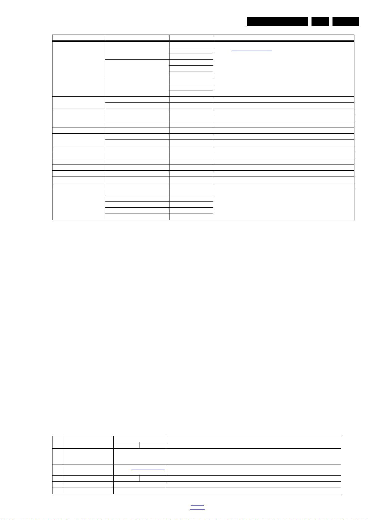
5.1.2 Service Alignment Mode (SAM)
Purpose
• To modify the NVM.
• To display/clear the error code buffer.
• To perform alignments.
Specifications
• Operation hours counter (maximum five digits displayed).
• Software version, error codes, and option settings display.
• Error buffer clearing.
• Option settings.
• Software alignments (White Tone).
• NVM Editor.
• Set screen mode to full screen (all content is visible).
How to Activate SAM
To activate SAM, use one of the following methods:
• Press the following key sequence on the remote control
transmitter: “062596”, directly followed by the “INFO/OK”
button. Do not allow the display to time out between entries
while keying the sequence.
After entering SAM, the following items are displayed,
with “SAM” in the upper right corner of the screen to indicate
that the television is in Service Alignment Mode.
count Stand-by hours.
not count Stand-by hours.
possible.
2016-Jul-08
back to
div.table
Page 15
Service Modes, Error Codes, and Fault Finding
Main Menu Sub-menu 1 Sub-menu 2 Description
Alignments Warm R Gain To align the White Tone. See
G Gain
B Gain
Normal R Gain
G Gain
B Gain
Cool R Gain
G Gain
B Gain
Ambilight Select module Ambilight select module
Brightness Brightness of Ambilight
Option numbers Group 1 Group 1 Option number
Group 2 Group 2 Option number
Store Store the Option number
Store Store
Software maintenance Software events Software events
Hardware events Hardware events
Test setting Digital info Test setting
BT Pairing tables Clear paired remote control Clear paired remote control
Wi-Fi Direct settings Reset Wi-Fi Direct group Reset Wi-Fi Direct group
Development 1 file versions Development 1 file versions
Development 2 file versions Development 2 file versions
Upload to USB To upload several settings from the TV to an USB stick
Download from USB To download several settings from the USB stick to the TV
NVM editor Type number NVM-editor will function as in the past: type number, production code, 18AC SSB,
Production code
18AC SSB
18AC display
18AC supply
paragraph 6.3 Software Alignments
18AC display, 18AC supply is a decimal value via digit entry
in the Alignments section for a detailed descript ion
EN 15QM16.1L LA 5.
How to Navigate
• In the SAM menu, select menu items with the UP/DOWN
keys on the remote control transmitter. The selected item
will be indicated. When not all menu items fit on the screen,
use the UP/DOWN keys to display the next/previous menu
items.
• With the “LEFT/RIGHT” keys, it is possible to:
– (De) activate the selected menu item.
– (De) activate the selected sub menu.
– Change the value of the selected menu item.
• When you press the MENU button once while in top level
SAM, the set will switch to the normal user menu (with the
SAM mode still active in the background).
• Press the following key sequence on the remote control
transmitter: “062596” directly followed by the “Home/Menu”
button to switch to (do not allow the display to time out
between entries while keying the sequence).
How to Store SAM Settings
To store the settings changed in SAM mode (except the
RGB Align settings), leave the top level SAM menu by using
the POWER button on the remote control transmitter or the
television set. The mentioned exceptions must be stored
separately via the STORE button.
How to Exit SAM
Use one of the following methods:
• Switch the set to STANDBY by pressing the mains button
on the remote control transmitter or the television set.
• Via a standard RC-transmitter, key in “00” sequence.
Note: When the TV is switched “off” by a power interrupt while
in SAM, the TV will show up in “normal operation mode” as
soon as the power is supplied again. The error buffer will not be
cleared.
5.1.3 Contents of the Factory mode:
Purpose
• To perform extended alignments.
Specifications
• Displaying and or changing Panel ID information.
• Displaying and or changing Tuner ID information.
• Error buffer clearing.
• Various software alignment settings.
• Testpattern displaying.
• Public Broadcasting Service password Reset.
•etc.
How to Activate the Factory mode
To activate the Factory mode, use the following method:
• Press the following key sequence on the remote control
transmitter: from the “menu/home” press “1999”, directly
followed by the “Back/Return” button. Do not allow the
display to time out between entries while keying the
sequence.
After entering the Factory mode, the following items are
displayed,
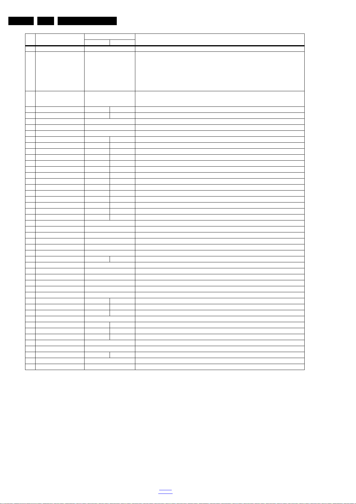
Table 5-2 Factory mode overview
Item Item value
0 F/W VERSION Press OK Displays the software versions of the supplier, Flash PQ, Smart Picture, BL Dimming, Source Meter, the
1 PANEL_ID See table back to div.table 6-3 Displays and changes the Panel ID with the left and right cursor; be careful changing this, it can result in
2 DEMOD_TYPE 5 5 Choose demod type.
3 NVM ADDRESS 0 NVM address 0 to 8191, Use Item 6 to change and 7 to store the data to the correct NVM address
4 NVM VALUE 0 Displays the value at the NVM address of item 5
Default value
Description50" 55"
Picture Quality checksum, the Dimming library, the Source meter library, the Flash AQ, MCU and OAD
software versions.
not correct displaying the screen!
back to
div.table
2016-Jul-08
Page 16
EN 16 QM16.1L LA5.
Default value
Item Item value
5 NVM STORE Press OK Use this option to save the data of item 6 to NVM address of item 5
6 COPY NVM to USB Press OK Use this to store the NVM data to the REPAIR folder of a FAT formatted USB memory stick. The TV will
7 COPY NVM to TV Press OK Use this to store the NVM data from the USB memory stick to the TV. The TV will save the two files which
8 TV Settings Key 1 1 TV Settings Key
9 TV Settings VALUE 0 0 TV Settings VALUE
10 TV Settings STORE Press OK TV Settings STORE
11 COPY TV Settings to USB Press OK COPY TV Settings to USB
12 COPY TV Settings to TV Press OK COPY TV Settings to TV
13 VIRGIN_MODE Off Off Use this to return the set to virgin mode. Depends whether the set has been used already.
14 ORT_MODE Off On ORT mode
15 DRMWARNING On Off Warning the data rights management
16 AGEING MODE Off Off Use this for aging a new LCD panel
17 COLOR TEMP MODE cool normal COLOR TEMP MODE
18 CLR_TEMP_R 116 127 Red colour temperature setting
19 CLR_TEMP_G 119 127 Green colour temperature setting
20 CLR_TEMP_B 127 110 Red colour temperature setting
21 ADC_GAIN_R 255 255 Red ADC gain
22 ADC_GAIN_G 255 255 Green ADC gain
23 ADC_GAIN_B 255 255 Blue ADC gain
24 ADC_OFFSET_R 127 127 Red ADC offset
25 ADC_OFFSET_G 127 127 Green ADC offset
26 ADC_OFFSET_B 127 127 Blue ADC offset
27 AUD_GAIN_HDMI 0 HDMI audio gain
28 AUD_GAIN_ATV 12 Analogue TV audio gain
29 AUD_GAIN_DTV 0 Digital TV audio gain
30 AU D_GAIN_USB 0 USB audio gain
31 AUD_GAIN_SPDIF 0 SPDIF audio gain
32 AUD_GAIN_LINE_IN 0 LINE_IN audio gain
33 AQ_INDEX 52 52 Audio Quality index
34 Copy PQ to USB Press OK Saves the picture quality data to a file “pq.bin” to the root of a FAT formatted USB memory stick
35 Copy PQ to TV Press OK Loads the picture quality data from a file “pq.bin” in to the TV
36 Copy AQ to USB Press OK Loads the audio quality data from a file “AQ.bin” in to the TV
37 Copy AQ to TV Press OK Loads the audio quality data from a file “AQ.bin” in to the TV
38 COPY DB CHL to USB Press OK Copy the USB channel list to USB
39 COPY DB CHL to TV Press OK Copy the TV channel list to TV
42 LIGHT SENSOR TYPE 8 8 Light sensor type
40 TEMP SENSOR TYPE 0 0 Tempreture sensor
41 LED TYPE 0 0 The type of LED
42 AMBILIGHT TYPE Side Segments The type of Ambient light
43 AMBILIGHT TYPE VALUE 0 0 The type value of Ambient light
44 3D 0 0 3D on/off
45 BLUETOOTH 1 1 BLUETOOTH
46 ARC TEST On ARC test
47 HDMI ARC OUTPUT ORDER EU HDMI ARC OUTPUT ORDER
48 UART ENABLE on off UART ENABLE
49 RESET MAC ADDRESS Press OK RESET MAC ADDRESS
50 EXIT_FACTORY Press OK Exits the Factory mode
Service Modes, Error Codes, and Fault Finding
Description50" 55"
write two files in the REPAIR folder of the memory stick. It will create this folder if it does not exist. The items
are “Channel list”, “Personal settings”, “Option codes”, “Display-related alignments” and “History list”. In
case the download to the USB stick was not successful “Failure” will appear. In this case, check if the USB
stick is connected properly. Now the settings are stored onto the USB stick and can be used to download
onto another TV or other SSB. Upl oading is of course only possible if the software is r unning and if a p icture
is available. This method is created to be able to save the customer’s TV settings and to store them into
another SSB.
were created in item 8 to the NVM of the set. Use these op tion s when replaci ng a S SB. When “ USB to TV
Success” is displayed remove the power and restart the TV
How to Exit the Factory mode
Use one of the following methods:
• Select EXIT_FACTORY from the menu and press the “OK”
button.
Note: When the TV is switched “off” by a power interrupt, or
normal switch to “stand-by” while in the factory mode, the TV
will show up in “normal operation mode” as soon as the power
is supplied again. The error buffer will not be cleared.
5.1.4 Customer Service Mode (CSM)
Purpose
The Customer Service Mode shows error codes and
information on the TVs operation settings.The call centre can
instruct the customer (by telephone) to enter CSM in order to
identify the status of the set.This helps the call centre to
2016-Jul-08
back to
div.table
diagnose problems and failures in the TV set before making a
service call.
The CSM is a read-only mode; therefore, modifications are not
possible in this mode.
Specifications
• Ignore “Service unfriendly modes”.
• Line number for every
line (to make CSM language independent).
• Set the screen mode to full
screen (all contents on screen is visible).
• After leaving the Customer Service Mode, the original
settings are restored.
• Possibility to use “CH+” or “CH-” for channel surfing, or
enter the specific channel number on the RC.
Page 17

Service Modes, Error Codes, and Fault Finding
How to Activate CSM
To activate CSM, press the following key sequence on a
standard remote control transmitter: “123654” (do not allow the
display to time out between entries while keying the sequence).
After entering the Customer Service Mode, the following items
are displayed.
Note: Activation of the CSM is only possible if there is no (user)
menu on the screen!
Contents of CSM
• 1.1 Set Type This information is very helpful for a
helpdesk/workshop as reference for further diagnosis. In
this way, it is not necessary for the customer to look at the
rear of the TV-set. Note that if an NVM is replaced or is
initialized after corruption, this set type has to be re-written
to NVM.
• 1.2 Production code Displays the production
code (the serial number) of the TV. Note that if an NVM is
replaced or is initialized after corruption, this production
code has to be re-written to NVM.
• 1.4 a Option Code 1 Gives the option codes of option
group 1 as set in SAM.
• 1.4b Option Code 2 Gives the option codes of option
group 2 as set in SAM.
• 1.5 18AC SSB Gives an identification of the SSB as stored
in NVM. Note that if an NVM is replaced or is initialized after
corruption, this identification number has to be re-written to
NVM. This identification number is the 12NC number of the
SSB.
• 1.6 18AC Display 18NC NVM read/write.
• 1.7 18AC Supply 18AC NVM read/write.
• 1.8 18AC sensor board 18AC NVM read/write.
• 2.1 Current Main SW Displays the built-in main software
version. In case of field problems related to software,
software can be upgraded. As this software is consumer
upgradeable, it will also be published on the internet.
• 2.2 Standby Software Displays the built-in stand-by
processor software version. Upgrading this software will be
possible via USB.
• 2.3 e-UM version eDFU (help) version.
• 2.4 Strings database version Displays the version of
strings database.
• 2.5 NT333 FRC version Displays the version of NT333
FRC.
• 2.10 Channel package version version of channel
package.
• 3.1 Signal Quality Analog/digital signal strength.
• 3.4 Ethernet MAC address A Media Access Control
address (MAC address) is a unique identifier assigned to
network interfaces for communications on the physical
network segment.
• 3.5 Wireless MAC address Wireless Media Access
Control address.
•
3.6 Netflix key Ind
case this key are not valid and the customer wants to make
use of the functionality, the SSB has to be replaced.
• 3.9 Event counter The counter of event.
icates the validity of the netflix key. In
EN 17QM16.1L LA 5.
How to Navigate
By means of the “CURSOR-DOWN/UP” knob (or the scroll
wheel) on the RC-transmitter, can be navigated through the
menus.
How to Exit CSM
To exit CSM, use one of the following methods.
• Press the MENU/HOME button on the remote control
transmitter.
• Press the POWER button on the remote control
transmitter.
• Press the POWER button on the television set.
back to
div.table
2016-Jul-08
Page 18
EN 18 QM16.1L LA5.
19080_206_110323.eps
120224
Power Off
Standby
Soft Mode
Power On
Semi-
Standby
Standby
Switch
Off(Mains
Power Plug)
Standby Soft Mode
Command Received,
previously in Standby
Soft Mode (Power tact
switch)
TV Wakeup
commands
Received
(TV Wakeup
keys)
Digital
background
tasks started
Digital
background
tasks completed
Swith On,
previously in
Standby/Semi-
Standby (Mains
Power Plug)
Standby
Soft Mode
Command
Received
(Power tact
switch)
Switch Off (Mains
Power Plug)
Switch Off
(Mains Power
Plug)
Swith On,
previously in
Standby Soft Mode
(Mains Power Plug)
Standby
commands
Received (RC
Standby key)
Standby Soft Mode
Command Received,
previously in Standby
Soft Mode (Power
tact switch)
TV Wakeup
commands
Received
(TV Wakeup
keys)
Switch On, previously
in Power On Mode
(Power tact switch)
Standby Soft Mode
Command Received,
(Power tact switch)
Switch Off (Mains
Power Plug)
Switch On,previously in
TV Operation Mode
(Mains Power Plug)
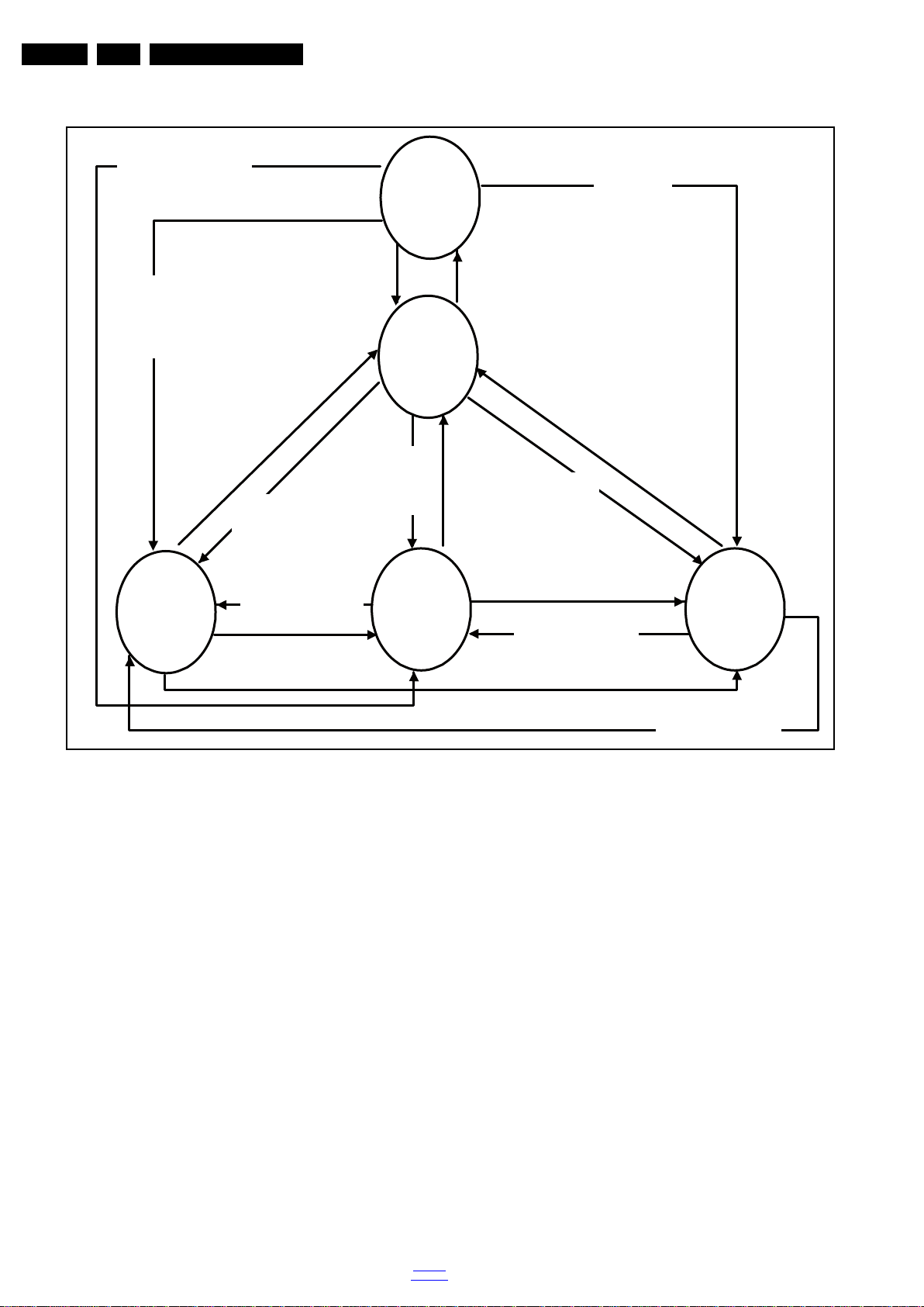
5.2 Stepwise Start-up
Service Modes, Error Codes, and Fault Finding
2016-Jul-08
Figure 5-1 Stepwise Start-up
back to
div.table
Page 19
Service Modes, Error Codes, and Fault Finding
19080_207_110324.eps
110324
19080_208_110324.eps
110324
19080_209_110324.eps
110324
EN 19QM16.1L LA 5.
5.3 Service Tools
5.3.1 ComPair
The ComPair Tool is no longer supported here. Still, the interface box can be used as level shifter between the TV chassis and PC.
5.4 Software Upgrading
5.4.1 Description
It is possible for the user to upgrade the main software via the
USB port. This allows replacement of a software image in a
stand alone set. A description on how to upgrade the main
software can be found in the DFU or on the Philips website.
5.4.2 Introduction
Philips continuously tries to improve its products, and it’s
recommend that the TV software is updated when updates are
available. Software update files can be obtained from the
dealer or can be downloaded from the following websites:
http://www.philips.com/support
Preparing a portable memory for software upgrade
The following requirements have to be met:
1. A personal computer connected to the internet.
2. An archive utility that supports the ZIP-format (e.g. WinZip
for Windows or Stufflt for Mac OS).
3. A FAT formatted USB memory stick (preferably empty).
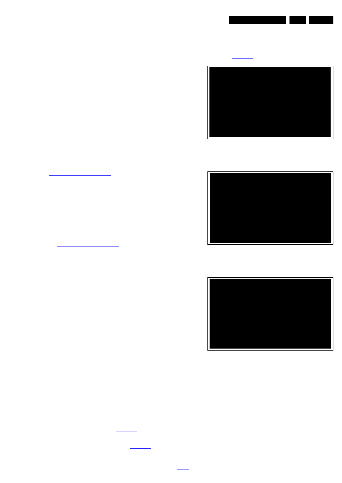
6. Upgrading will now begins and the status of the updating
progress will be displayed.
7. When the TV software is updated. Remove your USB flash
drive, then select [Restart] and press OK to restart the
TV.See Figure 5-4
.
Figure 5-2 Update the TV software [1/3]
Note:
1. Only FAT/DOS-formatted memory sticks are supported.
2. Only use software update files that can be found on the
http://www.philips.com/support
web site.
5.4.3 Check the current TV software version
Before starting the software upgrade procedure, it is advised to
check that what the current TV software:
1. Press the “1 2 3 6 5 4” button on the remote control to enter
the CSM mode.
2. Use the up/down cursor keys to select “Current Main
Software”.
If the current software version of the TV is the same as the
latest update file found on http://www.philips.com/support
not necessary to update the TV software.
5.4.4 Download the latest software
1. Open the internet page http://www.philips.com/support
2. Find information and software related to the TV.
3. Select the latest software update file and download it to the
PC.
4. Insert the USB memory stick into one of the USB ports of
the PC.
5. Decompress the downloaded ZIP file and copy it to the root
directory of the USB flash drive.
5.4.5 Update the TV software
1. Turn the TV on and wait for it to boot completely.
2. Insert the USB memory stick that contains the software
update files in one of the TV’s USB ports.
3. The TV will detect the USB memory stick automatically.
Then a window jumps out as Figure 5-2
.
Note: If the USB flash drive is not detected after power up,
disconnect it and re-insert it.
4. Select [Update] and press OK. See Figure 5-2
5. To proceed, In next menu select [Start] and press OK to
start software updates. See Figure 5-3
.
Figure 5-3 Update the TV software [2/3]
, it is
.
Figure 5-4 Update the TV software [3/3]
Note:
• Do not remove the USB flash drive during the software
update.
• If a power failure occurs during the update, do not remove
the USB flash drive from the TV. The TV will continue the
software update as soon as the power comes up again.
• If an error occurs during the update retry the procedure or
contact the dealer.
• We do not recommend downgrading to an older version.
• Once the upgrade is finished, use the PC to remove the TV
software from the USB portable memory.
.
back to
div.table
2016-Jul-08
Page 20
EN 20 QM16.1L LA5.
Service Modes, Error Codes, and Fault Finding
5.4.6 Content and Usage of the One-Zip Software File
Below you find a content explanation of the One-Zip file, and
instructions on how and when to use it. Only files that are
relevant for Service are mentioned here.
• EDID_clustername.zip: Contains the EDID content of the
different EDID NVMs.
• FUS_clustername_version.zip: Contains the file
downloaded which is needed to upgrade the TV main
software and the software download application.
• NVM_clustername_version.zip: Default NVM content.
5.4.7 How to Copy NVM Data to/from USB
When copying data to and from a USB memory stick, the folder
“repair” is used. When inserting an empty USB memory stick,
and downloading data to the stick, the TV will create this folder.
When sending data from a USB memory stick to a TV, the
intended data must be available in the “repair” folder.
Note that when copying EDID data to the TV, all necessary
EDID files must be in this folder.
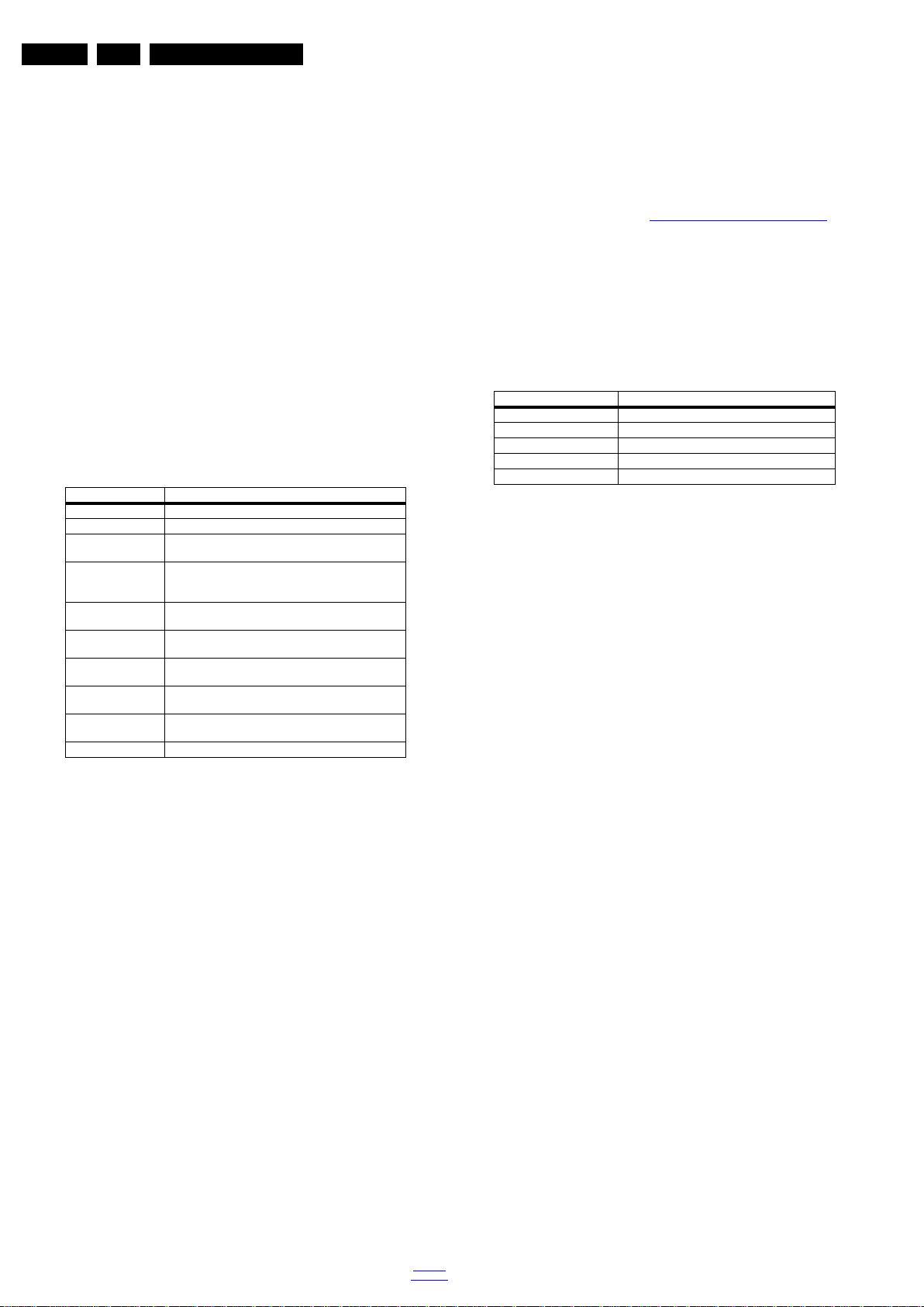
Service mode overview for your reference.
Table 5-3 Service mode overview
Service Modes Description
SAM Service alignment mode
Factory Mode Used for extended alignments
CSM 3-page compact CSM pages. There wi ll be CS M dump to
USB SW upgradeable SW-upgrading of flash memories MT5593FPIJ can be
NVM-Editor in SAM NVM-editor will function as in the past: Address and Value
Service Data New Service data in SAM for CTN, Prod. no., 12NC
USB copy/paste in
SAM
UART logging Th ere will be printout avail able in UART. No specif ications
Blind SAM RC sequence “062598” + “Menu” +
Clear Buffer RC sequence “062599” + “OK” or via SAM
USB-stick upon entering CSM-mode
done via USB. The main SW can be upgraded via the ZIP
file downloaded.
field is a decimal value via digit entry
programming with virtual keyboard
Channel list, NVM data, Readable info, EDID
of the printout, per MTK provision/definition.
“Panel code”
Example:
– ERROR: 000 000 000 000 000: No errors detected
– ERROR: 013 000 000 000 000: Error code 13 is the
last and only detected error
– ERROR: 034 013 000 000 000: Error code 13 was
detected first and error code 34 is the last detected
(newest) error
• Via the blinking LED procedure (when you have no
picture). See paragraph 5.6 The Blinking LED Procedure
5.5.3 Error codes
In this chassis only “layer 2” error codes are available and point
to problems on the SSB. They are triggered by LED blinking
when CSM is activated. Only the following layer 2 errors are
defined:
Table 5-4 Error code table
Layer-2 error code Defective de vice
13 General I2C bus error on the SSB
16 +12 V missing or low, PSU defective
27 Channel decoder error on the SSB
34 Tuner I2C bus error on the SSB
35 EEPROM I2C error on SSB, M24C64
5.5.4 How to Clear the Error Buffer
The error code buffer is cleared in the following cases:
• By using the CLEAR command in the SAM menu
• By using the CLEAR command in the Factory mode:
• By using the following key sequence on the remote control
transmitter: “062599” directly followed by the OK button.
• If the contents of the error buffer have not changed for 50
hours, the error buffer resets automatically.
Note: If you exit SAM by disconnecting the mains from the
television set, the error buffer is not reset.
5.6 The Blinking LED Procedure
5.6.1 Introduction
.
5.5 Error Codes
5.5.1 Introduction
Error codes are required to indicate failures in the TV set. In
principle a unique error code is available for every:
• Activated (SW) protection.
• Failing I
• General I
The last five errors, stored in the NVM, are shown in the
Service menu’s. This is called the error buffer.
The error code buffer contains all errors detected since the last
time the buffer was erased. The buffer is written from left to
right. When an error occurs that is not yet in the error code
buffer, it is displayed at the left side and all other errors shift one
position to the right.
An error will be added to the buffer if this error differs from any
error in the buffer. The last found error is displayed on the left.
An error with a designated error code never leads to a
deadlock situation. It must always be diagnosable (e.g. error
buffer via OSD or blinking LED).
In case a failure identified by an error code automatically
results in other error codes (cause and effect), only the error
code of the MAIN failure is displayed.
5.5.2 How to Read the Error Buffer
You can read the error buffer in three ways:
• On screen via the SAM/CSM (if you have a picture).
2
C device.
2
C error.
The software is capable of identifying different kinds of errors.
Because it is possible that more than one error can occur over
time, an error buffer is available, which is capable of storing the
last five errors that occurred. This is useful if the OSD is not
working properly.
Errors can also be displayed by the blinking LED procedure.
The method is to repeatedly let the front LED pulse with as
many pulses as the error code number, followed by a period of
1.5 seconds in which the LED is “off”. Then this sequence is
repeated.
Example (1): error code 4 will result in four times the sequence
LED “on” for 0.25 seconds / LED “off” for 0.25 seconds. After
this sequence, the LED will be “off” for 1.5 seconds. Any RC
command terminates the sequence. Error code LED blinking is
in red color.
Example (2): the content of the error buffer is “12 9 6 0 0” After
entering SAM, the following occurs.
• 1 long blink of 5 seconds to start the sequence.
• 12 short blinks followed by a pause of 1.5 seconds.
• 9 short blinks followed by a pause of 1.5 seconds.
• 6 short blinks followed by a pause of 1.5 seconds.
• 1 long blink of 1.5 seconds to finish the sequence.
• The sequence starts again with 12 short blinks.
5.6.2 How to Activate Blinking LED Procedurer
Use one of the following methods:
• Activate CSM.The blinking front LED will show the lay er 1
error(s), this works in “normal operation” mode or
2016-Jul-08
back to
div.table
Page 21

Service Modes, Error Codes, and Fault Finding
EN 21QM16.1L LA 5.
automatically when the error/protection is monitored by the
standby processor.
In case no picture is shown and there is no LED blinking,
read the logging to detect whether “error devices” are
mentioned. (see section “5.7 Fault Finding and Repair
Tips, 5.7.4 Guidelines Uart logging”).
• Activate SAM. The blinking front LED will show the entire
content of the LAYER 2 error buffer, this works in “normal
operation” mode.
5.7 Fault Finding and Repair Tips
Note:
• It is assumed that the components are mounted correctly
with correct values and no bad solder joints.
• Before any fault finding actions, check if the correct options
are set.
5.7.1 NVM Editor
In some cases, it can be convenient if one directly can change
the NVM contents. This can be done with the “NVM Editor” in
SAM mode. With this option, single bytes can be changed.
Caution:
• Do not change these, without understanding the function of
each setting, because incorrect NVM settings may
seriously hamper the correct functioning of the TV set!
• Always write down the existing NVM settings, before
changing the settings. This will enable you to return to the
original settings, if the new settings turn out to be incorrect.
5.7.6 No Picture via HDMI input
Check if HDCP key is valid. This can be done in CSM.
5.7.7 TV Will Not Start-up from Stand-by
Possible Stand-by Controller failure. Re-flash the software.
5.7.8 Audio Amplifier
The Class D-IC U606 has a powerpad for cooling. When the IC
is replaced it must be ensured that the powerpad is very well
pushed to the PWB while the solder is still liquid. This is needed
to insure that the cooling is guaranteed, otherwise the Class
D-IC could break down in short time.
5.7.9 Loudspeakers
Make sure that the volume is set to minimum during
disconnecting the speakers in the ON-state of the TV. The
audio amplifier can be damaged by disconnecting the speakers
during ON-state of the set!
5.7.10 Display option code
Attention: In case the SSB is replaced, always check the Panel
Code in CSM, even when picture is available. Performance
with the incorrect display option code can lead to unwanted
side-effects for certain conditions.
5.7.2 CSM
When CSM is activated and there is an USB stick connected to
the TV set, then the software will collect the complete CSM
content in a file Csm.xml and dump the file in a folder “CSM” on
the USB stick.
When this mechanism works it can be concluded that a large
part of the operating system is already working (SOC, USB ...).
5.7.3 No Picture
When you have no picture, first make sure you have entered
the correct display code. See paragraph 6.4 Option Settings
the instructions. See also back to div.table 6-3
5.7.4 Guidelines Uart logging
Possible cases:
Uart loggings are displayed:
• We can conclude that the TV-set is starting up and
thatcommunication with the flash RAM seems to be
supported. The processor is able to read and write in the
DRAMs.
• We can not yet conclude that flash RAM and DRAMs are
fully operational/reliable.There still can be errors in the data
transfers, DRAM errors, read/write speed and timing
control.
Uart loggings report fault conditions, error messages, error
codes and fatal errors:
• Some failures are indicated by error codes in the logging,
check referring to back to div.table 5-4.
2C bus errors.
•I
• Not all failures or error messages should be interpreted as
fault. For instance the root cause can be wrong option
codes settings.
for
.
5.7.5 Unstable Picture via HDMI input
Check if HDMI EDID data is properly programmed.
back to
div.table
2016-Jul-08
Page 22
EN 22 QM16.1L LA6.
6. Alignments
Index of this chapter:
6.1 General Alignment Conditions
6.2 Hardware Alignments
6.3 Software Alignments
6.4 Option Settings
6.5 Reset of Repaired SSB
6.1 General Alignment Conditions
Perform all electrical adjustments under the following
conditions:
• Power supply voltage: 90 - 264 V
• Connect the set to the mains via an isolation transformer
with low internal resistance.
• Allow the set to warm up for approximately 15 minutes.
• Measure voltages and waveforms in relation to correct
ground (e.g. measure audio signals in relation to
AUDIO_GND).
Caution: It is not allowed to use heat sinks as ground.
• Test probe: R
> 10 MW, Ci < 20 pF.
i
• Use an isolated trimmer/screwdriver to perform
alignments.
, 50/ 60 ± 3 Hz.
AC
Alignments
In case you have a colour analyser:
• Measure with a calibrated (phosphor- independent) color
analyser (e.g. Minolta CA-210) in the centre of the screen.
Consequently, the measurement needs to be done in a
dark environment.
• Adjust the correct x, y coordinates (while holding one of the
White point registers R, G or B on max. value) by means of
decreasing the value of one or two other white points to the
correct x, y coordinates (see Table 6-1 White D alignment
values). Tolerance: dx: ± 0.003, dy: ± 0.003.
• Repeat this step for the other colour Temperatures that
need to be aligned.
• When finished return to the SAM root menu and press
STANDBY on the RC to store the aligned values to the
NVM.
Table 6-1 White D alignment values
Value Cool (11000 K) Normal (9000 K) Warm (6500 K)
x 0.276 0.287 0.313
y 0.282 0.296 0.329
6.2 Hardware Alignments
Not applicable.
6.3 Software Alignments
Put the set in SAM mode (see Chapter 5. Service Modes, Error
Codes, and Fault Finding). The SAM menu will now appear on
the screen. Select RGB Align and go to one of the sub menus.
The alignments are explained below.
The following items can be aligned:
• White point.
To store the data:
• Press OK on the RC before the cursor is moved to the
left.
• Select “Store” and press OK on the RC.
• Switch the set to stand-by mode.
For the next alignments, supply the following test signals via a
video generator to the RF input:
• EU/AP-PAL models: a PAL B/G TV-signal with a signal
strength of at least 1 mV and a frequency of 475.25 MHz
• US/AP-NTSC models: an NTSC M/N TV-signal with a
signal strength of at least 1 mV and a frequency of
61.25 MHz (channel 3).
• LATAM models: an NTSC M TV-signal with a signal
strength of at least 1 mV and a frequency of
61.25 MHz (channel 3).
6.3.1 RGB Alignment
Before alignment, set the picture as follows:
Picture Setting
Dynamic backlight Off
Dynamic Contrast Off
Color Enhancement Off
Picture Format Unscaled
Light Sensor Off
Brightness 50
Color 0
Contrast 100
White Tone Alignment:
• Activate SAM.
• Select “RGB Align.” and choose a color temperature.
• Use a 100% white screen as input signal and set the
following values:
– “Red BL Offset” and “Green BL Offset” to “7” (if
present).
– All “White point” values initial to “128”.
If you do not have a colour analyser, you can use the default
values. This is the next best solution. The default values are
average values coming from production (statistics).
6.3.2 Display Adjustment
You can use the default values. The default values are average
values coming from production.
• Enter SAM mode.
• Select a colour temperature (e.g. COOL, NORMAL, or
WARM).
• Set the RED, GREEN and BLUE default values according
to the values in back to div.table 6-2
.
• When finished press OK on the RC, then press STORE to
store the aligned values to the NVM.
• Restore the initial picture settings after the alignments.
Table 6-2 White tone default settings
Picture mode Screen size
Normal (9000K) 50PUG6601/77 127 123 116
55PUG6601/77 127 127 110
Cool (11000K) 50PUG6601/77 116 119 127
55PUG6601/77 122 127 124
Warm (6500K) 50PUG6601/77 127 111 76
55PUG6601/77 127 119 69
Colour temperature
Red Green Blue
This group setting of colour temperature will be applied
automatically to the TV / VGA / HDMI / AV sources.
Note: The information of the RGB value is only for reference,
the specific value is based on model adjustment.
6.4 Option Settings
6.4.1 Introduction
The microprocessor communicates with a large number of I
ICs in the set. To ensure good communication and to make
digital diagnosis possible, the microprocessor has to know
which ICs to address. The presence / absence of these
MT5561 ICs is made known by the option codes.
Notes:
• After changing the option(s), save them by pressing the OK
button on the RC before the cursor is moved to the left,
select STORE and press OK on the RC.
2
C
2016-Jul-08
back to
div.table
Page 23
Alignments
EN 23QM16.1L LA 6.
• The new option setting is only active after the TV is
switched “off” / “stand-by” and “on” again with the mains
switch (the NVM is then read again).
6.4.2 Option Code Overview
Enter SAM mode to check the option codes. they could be
edited in the NVM.
6.4.3 Display Code Overview
Press the following key sequence on a standard RC
transmitter: “062598” directly followed by MENU and “xxx”,
where “xxx” is a 3 digit decimal value of the panel type: see
column “Display Code” in back to div.table 6-3
the Display Code, restart the set immediately.
Table 6-3 Display code overview
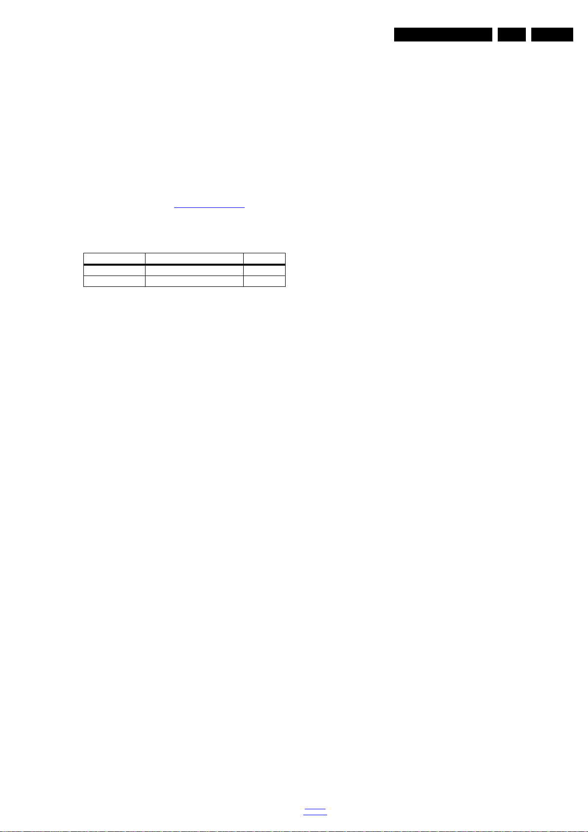
CTN_ALT BOM# Panel Type Display Code
50PUG6601/77 TPT500UK-DJ2QS5.N SM1B 036
55PUG6601/77 TPT550J1-QVN03.U S100C 233
6.5 Reset of Repaired SSB
A very important issue towards a repaired SSB from a Service
repair shop (SSB repair on component level) implies the reset
of the NVM on the SSB.
A repaired SSB in Service should get the service Set type
“00PF0000000000” and Production code “00000000000000”.
Also the virgin bit is to be set. To set all this, you can use the
“NVM editor” and “Dealer options” items in SAM (do not forget
to “store”).
. After resetting
• N Development number
• nn Production number
• MMM Mounting variation code
• OOOO Optional variation code
Make sure when replacing an SSB the SSB identification codes
match the replacement panel.
6.6 Cable position numbers
In this chassis, the cable position numbers can be defined via
the rule that the number is always starting with an “E” followed
by the connector number of the current sourcing board. The
order is always seen from where the power initiates from. So
from PSU to SSB, from SSB to IR/LED panel, from IR/LED
panel to keyboard control panel. For example, a cable from the
PSU connector CN902 to the SSB connector CN701, will have
the position number ECN902.
After a repaired SSB has been mounted in the set (set repair
on board level), the type number (CTN) and production code of
the TV has to be set according to the type plate of the set. For
this, you can use the NVM editor in SAM.
In case of a display replacement, reset the “Operation hours
display” to “0”, or to the operation hours of the replacement
display.
Remark:
- After the NVM has been replaced, go to SAM and scroll to the
<Reload MAC address> (see figure 1*).
- Select the item and press <OK> on the RC.
6.5.1 Reset of Repaired SSB
Instruction
After NVM replacement, reload MAC address via SAM
menu.This ensures the correct MAC address to be available in
CSM for future repair actions.
Way of working:
• After the NVM has been replaced, go to SAM and scroll to
the <Reload MAC address> .
• Select the item and press <OK> on the RC.
Notes:
• Only applicable to all related models that are “Smart TV
level 0”enabled (only YouTube access). For models
without internet connection feature, no action is needed.
• HDCP keys are located in the NVM.
New NVM EEPROMs are shipped with pre-loaded HDCP keys.
6.5.2 SSB Identification
SSB’s of this chassis are identified by a “715” code on the SSB.
715Axxxx-Nnn-MMM-OOOO
• 715 main category, Printed Wiring Board
• Axxxx sub category, sequential coding number
• Nnn Version code
back to
div.table
2016-Jul-08
Page 24

EN 24 QM16.1L LA7.
7. Circuit Descriptions
Index of this chapter:
7.1 Introduction
7.2 Power Supply
7.3 DC/DC Converters
7.4 Front-End Analogue and ISDB-T reception
7.5 HDMI
7.6 Video and Audio Processing - MT5593UPIJ
Notes:
•Only new circuits (circuits that are not published recently)
are described.
• Figures can deviate slightly from the actual situation, due
to different set executions.
• For a good understanding of the following circuit
descriptions, please use the wiring, block (see chapter
Block Diagrams) and circuit diagrams (see chapter
9.
Circuit Diagrams and PWB Layouts).Where necessary,
10.
you will find a separate drawing for clarification.
Circuit Descriptions
7.1 Introduction
The QM16.1L LA is a new chassis launched in Europe in
2016. The whole range is covered by MT5593UPIJ.
The major deltas versus its predecessor support ISDB-T with
also USB3.0, multi-media, WIFI, Video Out function.
The QM16.1L LA chassis comes with the following stylings:
• series xxPUG6601/77
7.1.1 Implementation
Key components of this chassis are:
• SCALER MT5593UPIJ HSBGA-900
• EMMC THGBMHG6C1LBAIL 8GB P-WFBGA153
• TUNER Latam TDST-H880F
• DEMODULATOR TC90537FG LQFP-48
• DRAM NT5CB256M16DP-EK 4Gb VFBGA-96
• AUDIO TTAS5760LDDCAR 20W TSSOP-48 for Audio
Amplifier
7.1.2 QM16.1L LA Architecture Overview
For details about the chassis block diagrams refer
Block Diagrams. An overview architecture can be found in
to 9.
Figure 9.1
.
2016-Jul-08
back to
div.table
Page 25
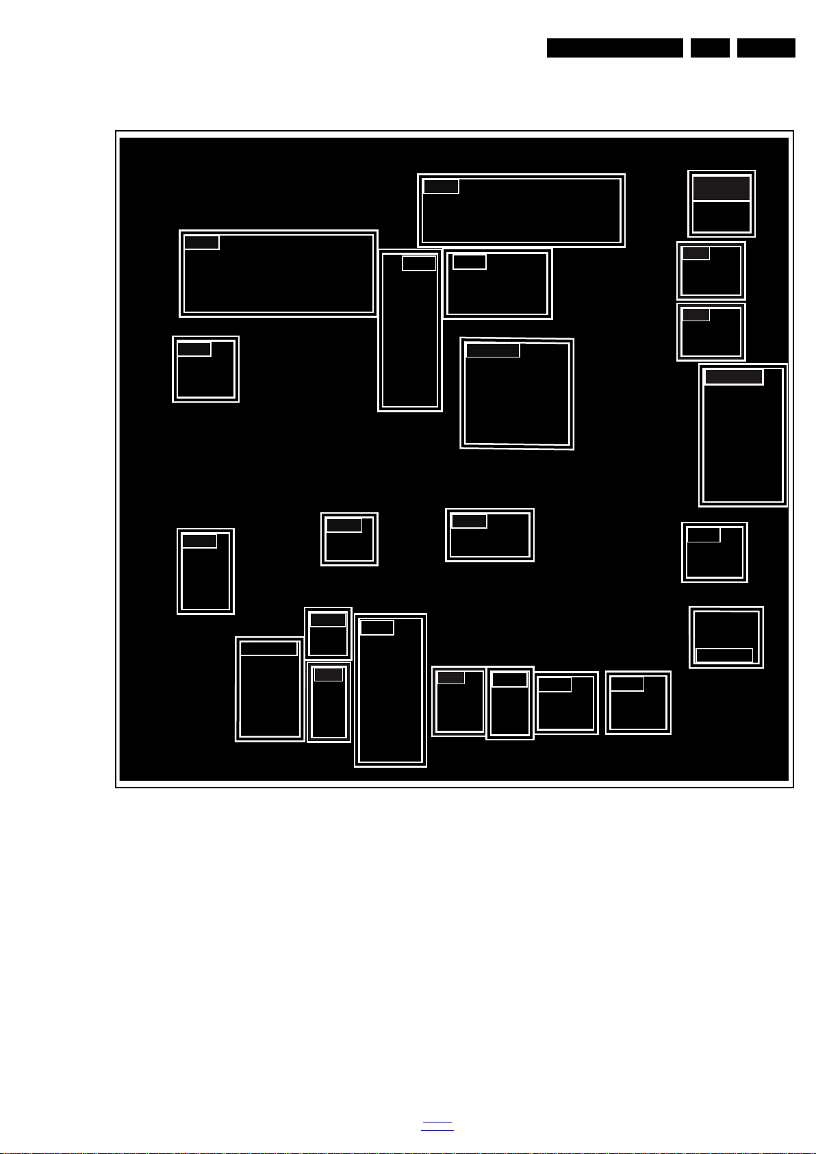
7.1.3 SSB Cell Layout
20170_200.eps
USB
SPDIF
ANALOG I/O
HDMI
DC/DC
DC/DC
DDR
USB
HDMI
HDMI
NETWORK
USB
SERVICE
CONNECTOR
DC/DC
DDR
MT5593UPIJ
Tuner
Headphone
Audio in
DC/DC
DC/DC
DC/DC
DC/DC
Circuit Descriptions
EN 25QM16.1L LA 7.
Figure 7-1 SSB layout cells (top view)
back to
div.table
2016-Jul-08
Page 26
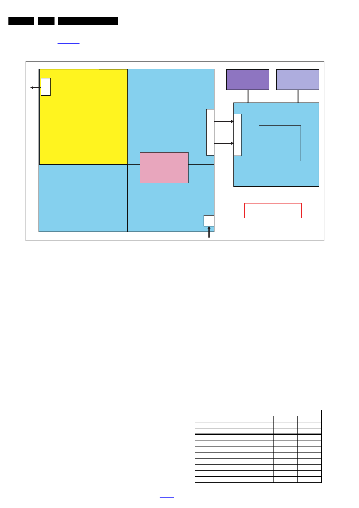
EN 26 QM16.1L LA7.
20160_200.eps
Display power
Platform
MT5593U
PFC
Platform power
1 power- PCB
LVDS AMP
Low stby
power
Ac-input + Mains filter
BL-ON/OFF
AC IN
CN9901
CN8601(FOR 715G7374)
CN8101(FOR 715G6973)
DIM
12V
12V_A
PS_On
12V
CN700
AMP
12V
7.2 Power Supply
Refer to figure Figure 7-2 for the power architecture of this
platform.
Circuit Descriptions
7.2.1 Power Supply Unit
All power supplies are a black box for Service. When defective,
a new board must be ordered and the defective one must be
returned, unless the main fuse of the board is broken. Always
replace a defective fuse with one with the correct
specifications! This part is available in the regular market.
Consult the Philips Service web portal for the order codes of the
boards.
Important delta’s with the QM16.1L LA classis platform are:
• New power architecture for LED backlight
• “Boost”-signal is now a PWM-signal + continuous variable.
The control signals are:
• Stand-by
• Lamp “on/off”
• DIM (PWM) (not for PSDL)
In this manual, no detailed information is available because of
design protection issues.
The output voltages to the chassis are:
• +8.5V output (standby mode)
• +12 output (on-mode)
• +12V_audio (audio AMP power)
• 37.4V output for Backlight
• Output to the display; in case of
- IPB: High voltage to the LCD panel
- PSL and PSLS (LED-driver outputs)
- PSDL (high frequent) AC-current.
2016-Jul-08
Figure 7-2 Power Architecture
7.2.2 Diversity
7.2.3 Connector overview
back to
div.table
The diversity in power supply units is mainly determined by the
diversity in displays.
The following displays can be distinguished:
• CCFL/EEFL backlight: power panel is conventional IPB
• LED backlight:
- side-view LED without scanning: PSL power panel
- side-view LED with scanning: PSLS power panel
- direct-view LED without 2D-dimming: PSL power panel
- direct-view LED with 2D-dimming: PSDL power panel.
PSL stands for Power Supply with integrated LED-drivers.
PSLS stands for a Power Supply with integrated LED-drivers
with added Scanning functionality (added microcontroller).
PSDL stands for a Power Supply for Direct-view LED backlight
with 2D-dimming.
Table 7-1 Connector overview
Number
Description to SSB to panel to SSB to panel
Pin16 121612
1 DIM +VLED DIM +VLED
2 BL_On/off +VLED BL_On/off n.c.
3 PS_ON -VLED-1 PS_ON -VLED1
4 n.c. -VLED-1 3D_ON -VLED1
5 GND -VLED-1 GND -VLED1
6 GND -VLED-1 GND n.c.
7 GND -VLED-2 GND n.c.
8 GND -VLED-2 GND -VLED2
Connector
CN9103 CN8601 CN9101 CN8101
Page 27
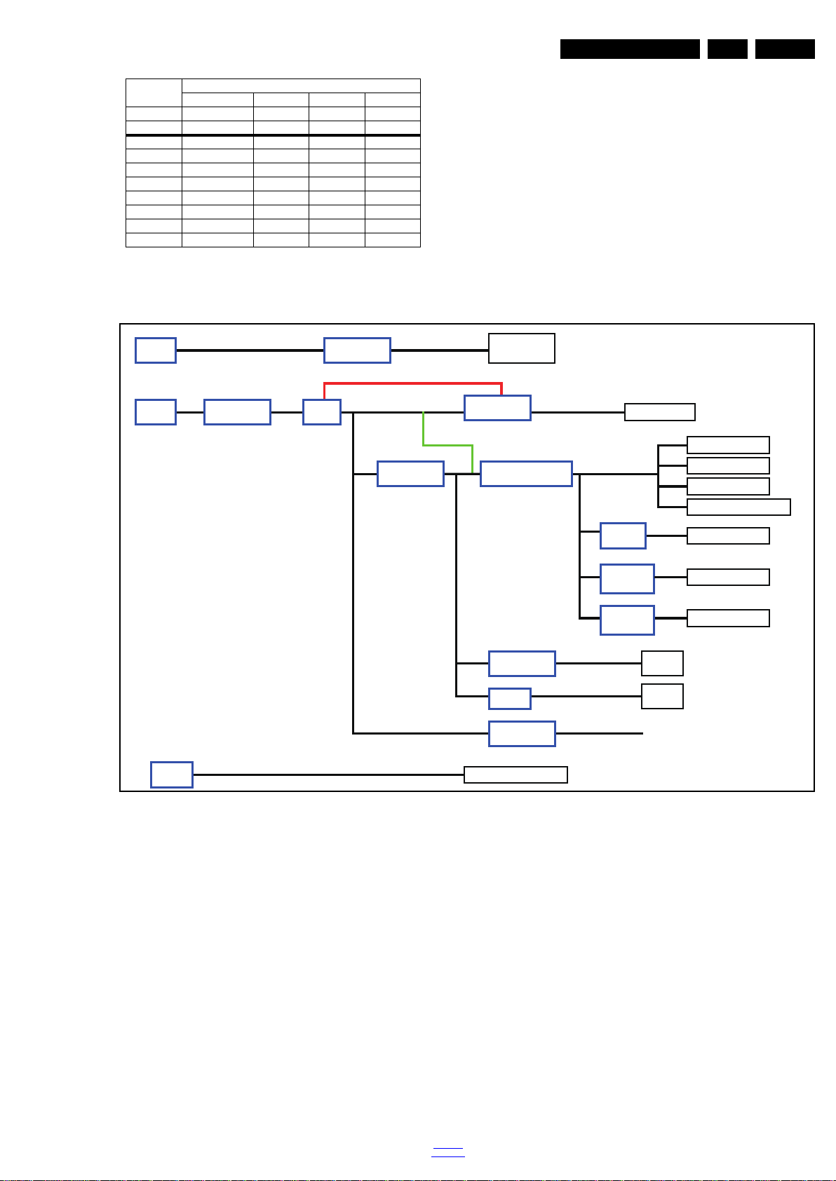
Circuit Descriptions
AUDIO - TAS5760LD
EMMC
MT5593
Demodulator IC
U701
1A
TO252
AP1117D33G-13
TUNER_3.3V
TUNER
U705 TU101
U4254
5A
U711
U707
AZ1117H-ADJ
EMMC
1A
SOT-223
1.8V
U503
1A
SOT-23-6
G529A1TB1U
USB *2
HDMI-MHL PWR5V
R4284
5V_USB
AUDIO - TAS5760LD
Audio VCC_12V
3A
For DDR quick start-stand by Mode.
uP1734PSW8
5V_STB
5A
SOP8
+12V
1A
SOT223
DFN8
AT1527F11U
G912T63U
DDR3-4G x5
AZ1084CS2-3.3TRE1
3A
5V_SW
MT5593
5.5A
SOP8
3A
1.2V
5A
TO-263
RT7240GSP
MOS-AON4421
+12V
Demodulator IC
1.05V
12V_AU
MT5593
VCCK(1.0V)
TPS54821RHL
8A
QFN-14
U702
7A
Q702
U708
U710
AVDD3V3/DVDD3V3
1.5V
20170_201.eps
EN 27QM16.1L LA 7.
Connector
Number
CN9103 CN8601 CN9101 CN8101
Description to SSB to panel to SSB to panel
Pin 16 12 16 12
9 +12V_A/+16V_A -VLED-2 +12V_A -VLED2
10 +12V_A/+16V_A -VLED-2 +12V_A -VLED2
11 +12V/+16V +VLED +12V n.c.
12 +12V/+16V +VLED +12V +VLED
13 +12V/+16V - +12V 14 +12V/+16V - +12V 15 +3.5V/+5V - +3.5V 16 +3.5V/+5V - +3.5V -
7.3 DC/DC Converters
The on-board DC/DC converters deliver the following voltages
(depending on set execution):
• +Wi-Fi_VCC, permanent voltage for WIFI.
• +3V3SB,voltage for IR/LED reciver,Key board
• +12V, input from the power supply for the panel
common(active mode)
• +12V, input from the power supply for LNB supply
• LDO_PWR,DVDD3V3, voltage for EMMC when TV on
• DDRV, VCCK, voltage for DDR
• +3V3_TUNER, supply voltage for tuner
• +5V-USB, input intermediate supply voltage for USB
Power
• PVDD from the power +12V_AU for the AUDIO AMP
• +1V2, +3.3VD voltage for Demodulator IC channel decoder
Figures gives a graphical representation of the DC/DC
converters with its current consumptions :
Figure 7-3 DC/DC converters
back to
div.table
2016-Jul-08
Page 28
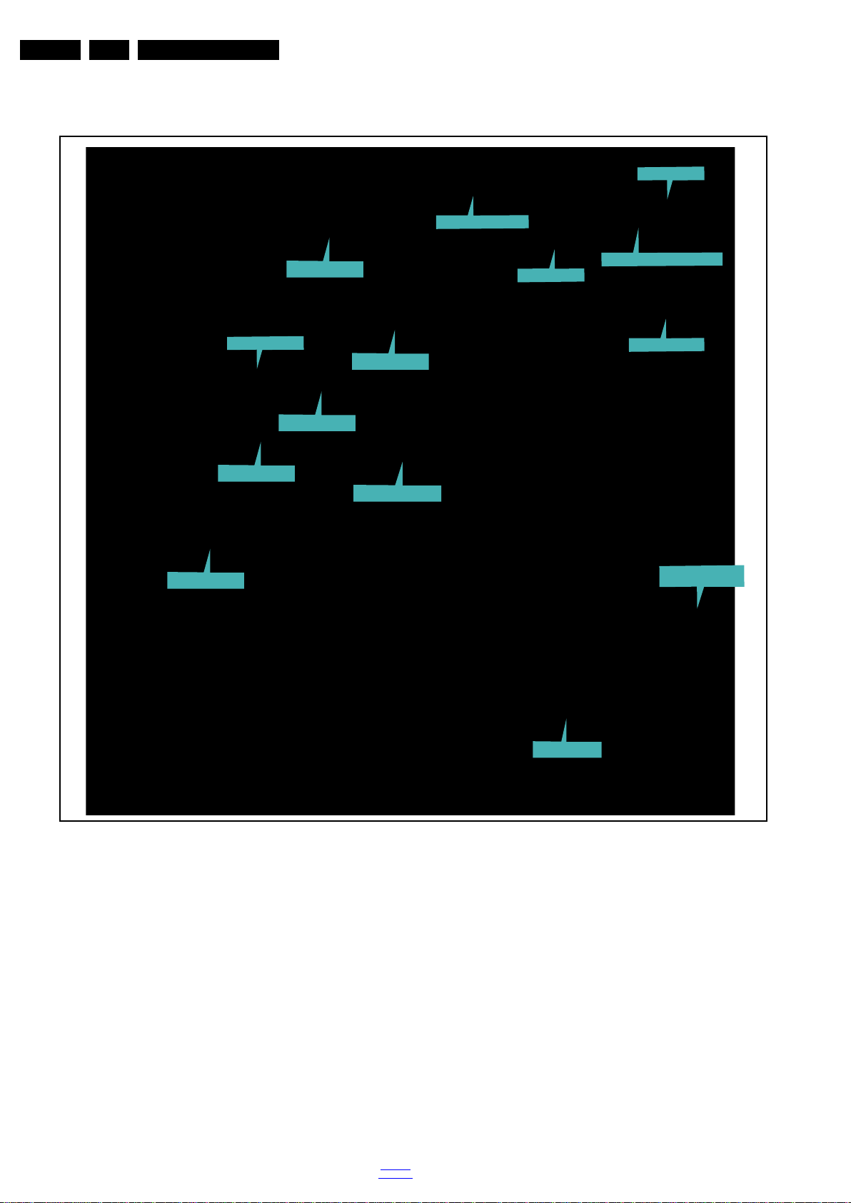
EN 28 QM16.1L LA7.
20050_207.eps
U701, DVDD3V3/
AVDD3V3
U703, LDO_PWR
U4601, AVDD33_ETH
L701, VCCK(1V)
C770, PVDD(12V)
D752, T uner_LNB
U707 Pin7,DV12
C779, AVDD1V0
C709, 3V3SB
U4251 Pin6,WI-FI_VCC(3.5V)
L705, +5V_SW
L702, DDRV(1.5V)
C752, Panel_VCC(12V)
U705,+3V3_Tuner
7.3.1 Power layout SSB
Circuit Descriptions
Figure 7-4 Power SSB Top View
2016-Jul-08
back to
div.table
Page 29
Circuit Descriptions
IF
RF_AGC
MT5593UPIJ
IF_AGC
TDST-H880F
I2C
I2C
20170_202.eps
EN 29QM16.1L LA 7.
U102 Pin1,CI_VCC
Figure 7-5 Power SSB Bottom View
7.4 Front-End Analogue and ISDB-T reception
7.4.1 Front-End Analogue reception
The Front-End for analogue tuner consist of the following key
components:
• TUNER Latam TDST-H880F
• SCALER MT5593UPIJ HSBGA-900 Processor
Below find a block diagram of the front-end application for
analogue part.
back to
div.table
20050_208.eps
Figure 7-6 Front-End Analogue block diagram
2016-Jul-08
Page 30
EN 30 QM16.1L LA7.
IF
TS DATA
RF_AGC
MT5593UPIJ
Demod
TC90537FG
IF_AGC
TDST-H880F
I2C
I
2
C
I2C
20170_203.eps
20170_204.eps
MT5593
HDMI3
HDMI 1
CN504
CN501
RX
RX
I2C
I
2
C
HDMI2
CN503
RX
I2C
Circuit Descriptions
7.4.2 ISDB-T reception(DEMODULATOR part)
The Front-End for DVT part consist of the following key
components:
• TUNER Latam TDST-H880F
• SCALER MT5593FPIJ HSBGA-900 Processor
• DEMODULATOR TC90537FG LQFP-48
Below find a block diagram of the front-end application for DTV
part.
Figure 7-7 Front-End ISDB-T block diagram
• ATSC/DVB-T/DVB-C/DTMB demodulators
• True 120Hz Full HD MJC
• Powerful CPU core
• A transport de-multiplexer
• A muti-standard video decoder
• Rich format audio codec
• MHL 2.0 & Standby Charging
• Ethernet MAC+PHY
• Local dimming (LED backlight)
The MT5593UPIJ combines DTV front-end video processing
functions, such as NTSC/PAL/SECAM Video Decoder,
MPEG1/2/4/H.264/VC1/RM/AVS/ and h.264/HEVC decode,
The MT5593UPIJ also supports MediaTek MDDi
de-interlace solution which can reach very smooth picture
quality for motions. A 3D comb filter added to the TV decoder
recovers great details for still pictures. The MT5593UPIJ
eanbles consumer electronics manufactures to build high
quality, low cost and feature-rich DTV.The special color
processing technology provides a natural, deep colors and true
studio quality video. Moreover, the MT5593UPIJ family has
built-in high resolution and high quality audio codec. The
MT5593UPIJ family supports ATSC, DVB-T,and DVB-C,
DTMB demodulation functions.
For a functional diagram of the MT5593UPIJ, refer to
Figure 8-1
.
TM
7.5 HDMI
Refer to figure 7-8 HDMI input configuration for the application.
Figure 7-8 HDMI input configuration
The following HDMI connector can be used:
• HDMI 1: HDMI input ( TV digital interface support
HDMI1.4/HDCP1.3) with digital audio/PC DVI input/ARC
• HDMI 2: HDMI input ( TV digital interface support HDCP)
with digital audio/PC DVI input/ARC
• HDMI 3: HDMI input ( TV digital interface support
HDMI1.4/HDCP1.3) with digital audio/PC DVI input/ARC
• HDMI 4: HDMI input ( TV digital interface support
HDMI1.4/HDCP1.3) with digital audio/PC DVI input/ARC
• +5V detection mechanism
• Stable clock detection mechanism
•HPD control
• CEC control
7.6 Video and Audio Process ing -
The MT5593UPIJ is the main audio and video processor (or
System-on-Chip) for this platform. It has the following features:
2016-Jul-08
• Worldwide multi-standard analog TV demodulator
MT5593UPIJ
back to
div.table
Page 31
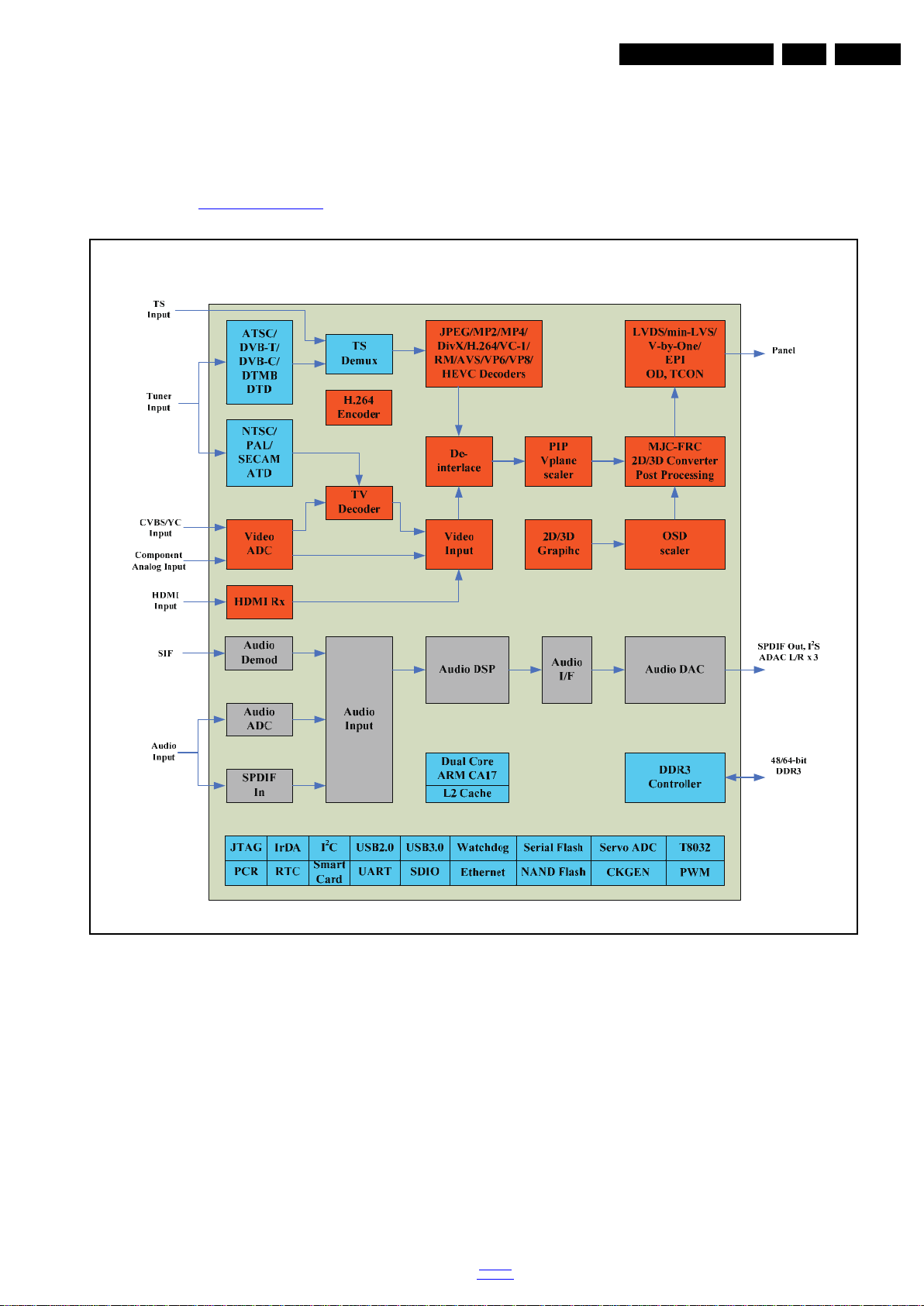
IC Data Sheets
19930_300.eps
Block diagram
MT5593FPIJ/UPIJ
8. IC Data Sheets
This chapter shows the internal block diagrams and pin
configurations of ICs that are drawn as “black boxes” in the
electrical diagrams (with the exception of “memory” and “logic”
ICs).
8.1 Diagram 10-3-3 Peripheral, B03, MT5593UPIJ (IC U401)
EN 31QM16.1L LA 8.
Figure 8-1 Internal block diagram
back to
div.table
2016-Jul-08
Page 32
EN 32 QM16.1L LA8.
19930_301.eps
Pinning Information
MT5593FPIJ/UPIJ
900 1 2 3 4 5 6 7 8 9 10 11 12 13 14 15 16 17 18 19 20 21 22 23 24 25 26 27 28 29 30 31 32 33 34 35 36 37 38
A
NC
CI_A5 CI_A6 CI_A7
CI_A12CI_MDI1CI_MD
I0 CI_INT
SPI_D
ATA
CI_TS
VAL
D_TSC
LK
USB_D
P_P0
USB_D
P_P1
0_RX_20_RX_10_RX_
0
0_RX_
C
1_RX_
2
1_RX_
C
2_RX_
0
3_RX_
1
10_HD
MI
10_SS
USB
SSUSB
_RXN
33_SS
USB
SSUSB
_TXN
SSUSB
_VRT
AIN_R3AIN_R
1
NC
A
B CI_A2 CI_A4
GPIO47CI_MDI7CI_MDI4CI_MI
VAL
CI_MD
I2
CI_MIS
TRT
CI_MDO6CI_MD
O5
SPI_CL
K
PVR_T
SCLK
CI_TSS
YNC
IF_AG
C
USB_V
RT_P0
USB_D
M_P0
USB_D
M_P1
0_RX_2B0_RX_
1B
0_RX_
0B
0_RX_CB1_RX_
2B
1_RX_
CB
2_RX_
0B
3_RX_
1B
10_HD
MI DVSS
SSUSB
_RXP DVSS
SSUSB
_TXP
AIN_L2AIN_R
0DVSS
AIN_R
2BB
C
CI_A0 CI_A1
CI_MDO2CI_MDI6GPIO64CI_MDI3CI_A14CI_A1
3 CI_D6
SPI_CLESPI_CL
K1
DATA
0
CI_TS
CLK
RF_AG
CDVSS DVSS
1_RX_11_RX_
0
2_RX_22_RX_
1
2_RX_
C
3_RX_
2
3_RX_
0
3_RX_
C
USB_D
P_P2
AL0_A
DAC
AR2_A
DAC
AIN_L3AIN_L
1
C
D
SD_D0
SD_CMDGPIO4
2CI_D2
CI_MDO1GPIO63GPIO66VCC3I
O_SD
CI_MDI5CI_MC
LKI
CI_A11CI_A10CI_MDO7CI_MDO3GPIO44PVR_T
SVAL
D_TSD
ATA0
D_TSS
YNC
1_RX_
1B
1_RX_
0B
2_RX_2B2_RX_1B2_RX_
CB
3_RX_
2B
3_RX_0B3_RX_
CB
USB_D
M_P2
HDMI_
3_SDA
HDMI_
3_SCL
AR1_A
DAC
AR0_A
DAC
AIN_L0VMID_
AADC DD
E
SD_D2
GPIO4
6CI_D1
CI_MDO0GPIO65GPIO62GPIO6
1CI_A8 CI_A9CI_D5CI_D7CI_D4
PVR_T
SSYNC
DEMO
SSVDSSVD
TSR_D
1_PWR
5V
2_PWR
5V
ADIN3
_SRV
3_PWR
5V
AL2_A
DAC
AL1_A
DAC XTALI
XTAL
OEE
F
VCC3I
O_A
SD_CLGPIO48GPIO4
5 CI_D0 DVSS DVSS
CI_MD
O4 CI_ D3
SDAT
A0
D_TSV
AL
D_TSD
ATA1
D_TSD
ATA7
MHL_S
ENSE
D_TSD
ATA6
HDMI_
0_SCL
HDMI_
0_SDA
0_HPD
_CBUS
HDMI_
1_HPD
HDMI_
2_HPD
HDMI_
2_SDA
HDMI_
3_HPD
N_DE
MOD
P_DEM
OD
F
G
A
33_DD
R
AVSS_
DDR
NC NC
DVSS
GPIO4
3
SDAT
A1
FSRC_
WR
D_TSD
ATA2
D_TSD
ATA5
HDMI_
CEC
0_PWR
5V
ASPDI
FO1
HDMI_
1_SDA
HDMI_
1_SCL
HDMI_
2_SCL
33_XT
AL_ST
33_DE
MOD_ GG
H
NC NC NC NC NC NC NC
D_TSD
ATA3
D_TSD
ATA4
SIF_COMCVBS0
PHH
J
NC
DVSS
NC NC
DVSS DVSS
ADIN6
_SRV
CVBS_
COM PR0P
CVBS3
P
J
K
NC NC NC NC
DVSS
NC NC
DVSS DDRV
X_OU
T
CVBS1PCVBS2
PPB0PCOM0
K
L
NC NC NC NC NC NC
DVSS DDRV
LOUTP
LOUT
N
33_LV
DSADVSS
ADIN4
_SRV
ADIN0
_SRV
ADIN2
_SRV Y0 P SOY0 PR1P
L
M
NC
TN_AR
SSVDSSVDSSVDSSVDLLPM
AVSS3
3_CLN
AVSS3
3_RGB
33_AA
DC
33_AD
AC
33_LV
DSBDVSS
ADIN5
_SRV
ORESE
TB
33_VI
DEO_S PB1P Y1P COM1
M
N
NC NC NC
DVSS DDRV
TP_AR
MPLL
DVSS DVSS DVSS DVSS DVSS
3_DEM
OD
3_XTA
L
33_US
B
OPCTR
L6
ADIN9
_SRV
ADIN8
_SRV SOY1 RP NN
P
NC NC NC NC NC
DVSS
NC NC NC NC
DVSS DVSS DVSS DVSS DVSS DVSS DVSS DVSS DVSS DVSS
33_HDMI33_HDMI33_ET
H
ADIN1
_SRV COM GP SOG
P
R
NC NC NC NC
DVSS DVSS DVSS DVSS DVSS DVSS DVSS DVSS DVSS DVSS
OPCTRL2OPCTRL0OPCTRL8OPCTR
L1
HSYN
CBPRR
T
NC
DVSS
NC NC NC
DVSS DVSS DDRV
DVSS DVSS DVSS DVSS DVSS DVSS DVSS DVSS DVSS DVSS
OPCTR
L5
VSYN
C
VGA_S
CL TT
U
NC NC
DVSS
NC NC NC NC NC NC
DDRV
DVSS DVSS DVSS DVSS DVSS DVSS DVSS DVSS DVSS DVSS VCCK
DVSS CPC0
POR_OPTOPCTRL7VGA_S
DA
ADIN7
_SRV
33_RG
B_STB
U
V
REF_A
1
NC
DVSS DVSS DVSS DVSS DVSS DVSS DVSS DVSS DVSS DVSS VCCK VCCK VCCK
CPC1 CPC2
10_LD
O
10_EL
DO REXT VV
W
ARDQ4ARDQ
CVSSVDSSVDSSVDSSVDSSVDSSVDSSVDSSVDSSVDSSVDSSVDNTRASSVDSSVDSSVD6 CK VCCK VCCK
OPCTR
L3
TXVP_0TXVN
_0
W
Y
ARDQ2ARDQ0ARDQ11ARCLK0ARCL
K0#
DDRV
_CKA DVSS DVSS ARTP
DVSS DVSS DVSS DVSS DVSS DVSS DVSS DVSS DVSS DVSS DVSS VCCK VCCK VCCK
OPCTRL9OPCTR
L4 OIRI
33_PL
L_STB
RXVP_1RXVN
_1
Y
AA
ARRAS#ARCAS#ARCK
KCCVKCCVKCCVSSVDSSVDSSVDSSVDSSVDSSVDSSVDSSVDSSVDSSVDSSVDE
LED_P
WM1
LED_P
WM0
PHYLE
D1
33_RE
G_STB
USB_D
P_P3
USB_D
M_P3
AA
AB
ARDQ15ARDQ13ARDQ9ARCS
D# ARCS#
ARODTARWE
#DDRV
DVSS DVSS DVSS DVSS DVSS DVSS DVSS DVSS DVSS DVSS DVSS VCCK VCCK VCCK
ASPDI
FO0
PHYLE
D0 DVSS
OPCTR
L11
OPWR
SB
AB
AC
ARDQS0ARDQ
S0#
ARDQ
M1 DVSS
DVSS DVSS DDRV DDRV
DVSS DVSS DVSS DVSS DVSS DVSS VCCK VCCK VCCK VCCK V
CCK VCCK VCCK VCCK
OPCTR
L12
OPCTR
L17
OPCTR
L10 DVSS
STB_SCLSTB_S
DA
AC
AD
ARDQM0ARDQ
S1DVSS
ARBA0ARBA
2ARA10 DVSS DDRV
DVSS DVSS DVSS DVSS DVSS VCCK VCCK VCCK VCCK VCCK VCCK VCCK V
CCK
OPCTR
L16
OPCTR
L15
OPCTR
L20
OPCTR
L18
OPCTR
L19 AAD
AE
ARDQ
S1#
ARBA
1ARA0 DVSS
MEMT
P
AVSS_
DDR
10_DD
R VCCKVCCKVCCKVCCKVCCKVCCKVCCKVCCK
OPCTR
L14 PAALE U0TX U0RX
AE
AF
ARDQ8ARDQ12ARDQ
14 ARA3 DVSS ARA12 ARA2 DVSS DVSS
MEMTNAVSS_
DDR
10_DD
R PDD2 PDD1
POCE1
__B
LED_P
WM2
POCE0
__B AAF
AG
ARDQ10ARDQ1ARDQ
3 DVSS ARA4 ARA1 ARA5 DVSS
OPCTR
L13
LED_P
WM3 PACLE
POWE
__B AAG
AH
ARDQ7ARDQ
5ARA9DVSS DDRV DDRV PDD3 PDD4
PARB_
_B
POOE_
_B
AH
AJ
ARDQ
20
REF_A
2
ARDQ
22 ARA7 ARA6 DVSS
DDRV
_CKB DDRV DDRV DDRV
NC
PDD7 PDD6 PDD5 DVSS PDD0
O_EM
MC AAJ
AK
ARDQ18ARDQ16ARDQ
27
ARRES
ET# ARA13 ARA11 DDRV DDRV DDRV DDRV DDRV DDRV DDRV DDRV DDRV DDRV DDRV
TN_HP
CPLL
TP_HP
CPLL DVSS
GPIO4
9DVSS DVSS
EMMC_R
STB
GPIO60VCC3I
O_B
AK
AL
ARDQ25ARDQ
29 ARA8 DVSS DDRV DDRV DDRV DDRV DVSS DVSS BRTP BRTN
TCON12GPIO50GPIO55OPWM1AOSD
ATA2
6
EMMC
_CLK
AL
AM
ARDQM3ARDQ31ARDQ
S2 ARA14 DDRV DDRV DDRV DDRV DVSS DVSS DVSS DVSS DVSS DVSS DVSS DVSS
TCON1 TCON3 TCON4 TCON8
TCON1
0
GPIO51GPIO54AOSD
ATA1
AOBCKAOSD
ATA3 5
GPIO59
U1RX U1TX AAM
AN
ARDQ
S2#
ARDQ
M2 DVSS
BRCK
E BRA10 BRBA1 BRA2 BRA7 BRA6 BRA14
TCON2 TCON9
TCON1
1
GPIO52GPIO53AOLRCKAOSD
ATA0
AOSD
ATA4
GPIO58
OSCL1 OSDA1
AN
AP
ARDQS3ARDQ
S3#
ARD
Q
2
8 DDRV DDRV
BRCL
K0
BRCAS
#
BRODTBRWE
# BRBA0 BRBA2 BRA3 BRA5 BRA1 BRA9 BRA11 BRA8 DVSS DVSS DVSS DVSS DVSS DVSS
DVSS
AOMCLKOPWM2OPWM
0AAP
AR
ARDQ24ARDQ30ARDQ23BRDQ11BRCL
K0#
BRRAS
#
BRCS#
BRCSD
#DVSS BRA0 BRA12
BRDQ
M3 BRA4 DVSS BRA13
BRRES
ET# DVSS BE4N BE3NBE2NBE1NBO4NBO3NBO2NBO1NAE4N AE3NAE2NAE1NAO4NAO3N AO2N AO1N
GPIO56ASPDI
FI AAR
AT
ARDQ26ARDQ17BRDQ
4DVSS
BRDQ15BRDQ
S0# DVSS
BRDQS1BRDQ8BRDQ1BRDQ7BRDQ20BRDQ16BRDQ25BRDQM2BRDQ
S3#
BRDQ30BRDQ19BRDQ
21
BE4P BE3PBE2PBE1PBO4PBO3PBO2PBO1PAE4PAE3PAE2PAE1P
AT
AU
ARDQ19ARDQ21BRDQ2BRDQ0BRDQ9BRDQS0BRDQM0BRDQ
S1#
BRDQ10BRDQ
3
BRDQ5BRDQ18BRDQ27BRDQ29BRDQ
S2#
BRDQS3BRDQ28BRDQ17BRDQ23AVSS_
DDR
10_LV
DS
BECK
NBE0N
BOCK
NBO0N
AECK
NAE0N
AOCK
NAO0N
GPIO5
7AAU
AV
NC
REF_B
1
BRDQ6BRDQ13BRDQM1BRDQ12BRDQ
14
REF_B
2
BRDQ22BRDQ31BRDQS2BRDQ24BRDQ
26
10_DD
R
REXT_
VPLL
BOCK
P
BO0P
AOCK
PAO0PNCAV
1 2 3 4 5 6 7 8 9 10 11 12 13 14 15 16 17 18 19 20 21 22 23 24 25 26 27 28 29 30 31 32 33 34 35 36 37 38
SD_D3K
DDRV
DDRV
DDRV
DVSS
DVSS
DDRV
DDRV
DDRV
AE0P
AECKP
BE0P
BECKP
AVDD
AVDD
DEMO
HDMI_ HDMI_
HDMI_
HDMI_
HDMI_ HDMI_
HDMI_
HDMI_
SD_D1
DDRV
AVDD
AVDD
AVDD
HDMI_
HDMI_
HDMI_
AVDD
AVDD
ADCIN
ADCIN
AVDD
HDMI_
HDMI_
DVSS
HDMI_HDMI_
HDMI_
HDMI_
HDMI_
HDMI_ HDMI_ HDMI_
HDMI_
HDMI_
HDMI_
HDMI_
HDMI_
HDMI_HDMI_
HDMI_
HDMI_ HDMI_
HDMI_
HDMI_
HDMI_
HDMI_
CI_A3
CI_TS
DEMODEMO
OSCL2
OSDA2
PVR_T
DEMO
PVR_T
DEMO DEMO
DEMO
DEMO
DEMO
DEMO DEMO
HDMI_
HDMI_
VDAC
AVDD
OSCL0
OSDA0
AO1P
AO2P
AO3PAO4P
AVDD
AVDD
DVSS
VCC3I
AVDD
AVDD
AVDD
AVDD
AVDD
AVDD
AVSS3
AVSS3
AVDD
AVDD
AVDD
AVDD
AVDD
AVDD
AVDD
TCON0 TCON5 TCON6 TCON7
DVS
DVSS
VDD
IC Data Sheets
Figure 8-2 Internal pin configuration [1/2]
2016-Jul-08
back to
div.table
Page 33
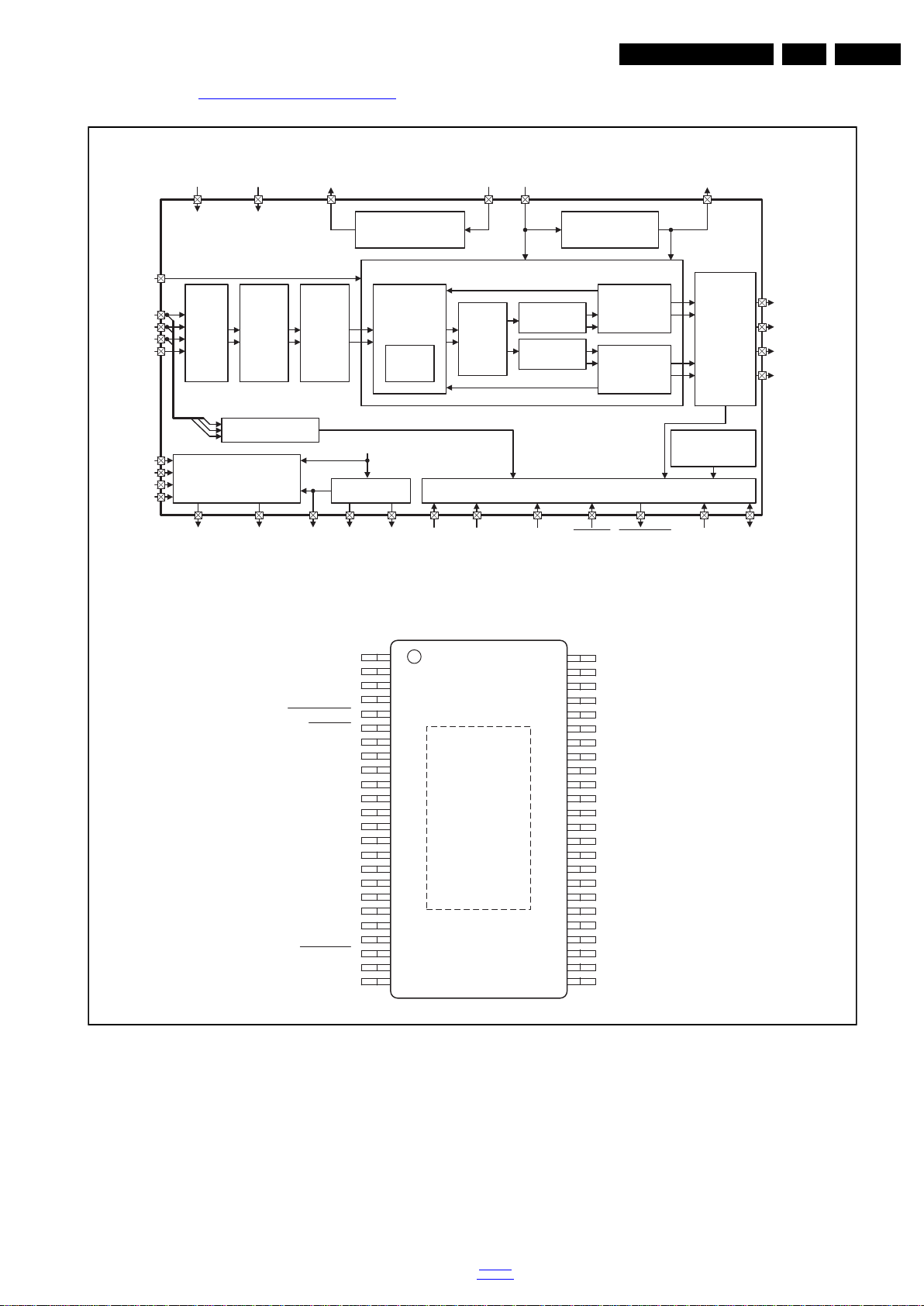
IC Data Sheets
19820_300.eps
Block diagram
Pinning information
+
+
S
+
-
+
-
TAS5760LD
TAS5760LD
8.2 Diagram 10-3-6 Speaker/Headphone B06, TAS5760LDDCAR (IC U601)
DDVAGER_ANADDVRDDDVD GVDD_REGPVDD
EN 33QM16.1L LA 8.
Internal
Voltage
Supplies
FT_CLIP
MCLK
SCLK
LRCK
SDIN
Serial
Audio
Port
DR_INA+
DR_INA-
DR_INB+
DR_INB-
DirectPathTM Ground
Centered Headphone /
Line Driver
DR_OUTA DR_OUTB
DRVDD
Digital
Boost
&
Volume
Control
Clock Monitoring
DRVSS DR_CP
SPK_FAULT
FREQ/SDA
SPK_GAIN0
SPK_GAIN1
SPK_SLEEP/ADR
Internal Reference
Regulators
Internal Gate
Drive Regulator
Closed Loop Class D Amplifier
Digital to
Power Stage
Power Stage
Digital
Clipper
DRVDD
PWM
Conversion
Analog
Gain
Soft
Clipper
Gate
Drives
Gate
Drives
Charge Pump Internal Control Registers and State Machines
SPK_GAIN1
48
47
46
45
44
43
42
41
40
39
38
37
36
35
34
33
32
31
30
29
28
27
26
25
SPK_SD
GVDD_REG
GGND
AVDD
PVDD
PVDD
BSTRPA+
SPK_OUTA
PGND
SPK_OUTABSTRPABSTRPBSPK_OUTBPGND
SPK_OUTB
BSTRPB+
PVDD
PVDD
DR_INBDR_INB+
DR_OUTB
DR_UVE
DRGND
DRVDD
DR_CP
SFT_CLIP
ANA_REG
VCOM
ANA_REF
SPK_SD
PBTL/SCL
DVDD
MCLK
SCLK
SDIN
LRCK
DGND
DR_INA-
DR_INA+
DR_OUTA
DRGND
DR_MUTE
DRVSS
DR_CN
DR_CN
1
2
3
4
5
6
7
8
9
10
11
12
13
14
15
16
17
18
19
20
21
22
23
24
PBTL/
SCL
SPK_GAIN0
PowerPAD
Full Bridge
A
Full Bridge
B
SPK_FAULT
Over-
Current
Protection
Die
Temp. Monitor
SPK_SLEEP/
ADR
FREQ/
SDA
SPK_OUTA
SPK_OUTA
SPK_OUTB
SPK_OUTB
Figure 8-3 Internal block diagram and pin configuration
back to
div.table
2016-Jul-08
Page 34
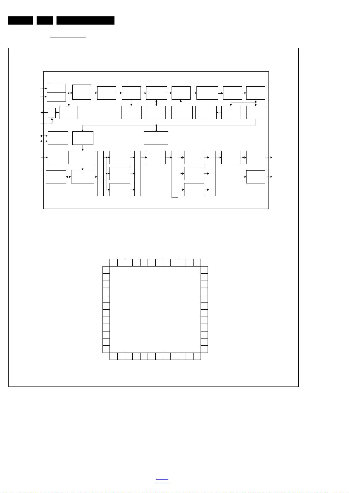
EN 34 QM16.1L LA8.
19950_300.eps
Block diagram
Pinning information
TC90537FG
TC90537FG
SRCK
PBVAL
SRDT
SLOCK
RLOCK
RERR
SLPEN
GPIO2
GPIO1
GPIO0
VSS
VDDC
12 11 10 9 8 7 6 5 4 3 2 1
VSS 13 48 VDDS
VDDS 14 47 VSS
RSEORF 15 46 SDA
SBYTE 16 45 SCL
SLADRS0 17 44 STSFLG0
AGCCNTI 18 43 STSFLG1
AGCCNTR 19 42 SYRSTN
TNSCL 20 41 VPGM
TNSDA 21 40 AINN Q
XCKO 22 39 AINP Q
XO 23 38 AINN I
XI 24 37 AINP I
25 26 27 28 29 30 31 32 33 34 35 36
PLLVDD
PLLVSS
VDDC
CKI
SLADRS1
TSMD
VSS
VDDC
ADCVDD
ADCVSS
VREFL
VREFH
Synchroni-za
tion flag
TS output
Crystal
(reference clock)
Tuner
AGC
control
IIC
control
Filter
AGC
ISIC (unguarded
pre/post echo
suppression)
FFT
Control
Adaptive
interpolation
filter
Equalization
CSI
(Reliability
detection)
CVI
(CW interference
detection)
AGC control output
Tuner IIC
Clock PLL
Viterbi
decoding
Memory
Frequency
deinterleaving
RS
decoding
Error
detection
Output
control
Layer
isolation
TMCC
demodulation
Interpolation
phase
Correction
Synchroni
zation
Demapping
CSI
processing
Bit deinterleaving
Byte deinterleaving
TS multiplex
FFT window
control
ADC
ADC
IF input
or IQ input
SW
External AGC input
Host IIC
Energy
despreading
Energy
despreading
Energy
despreading
Demapping
CSI
processing
Demapping
CSI
processing
Modulation division
Quadrature
detection
AFC
Frequency
CPE
Pilot
extraction
Time
deinterleaving
(With Doppler
Compensation
)
IC Data Sheets
8.3 Diagram 10-3-14 ISDB-T Tuner B14, TC90537FG (IC U4253)
2016-Jul-08
Figure 8-4 Internal block diagram and pin configuration
back to
div.table
Page 35
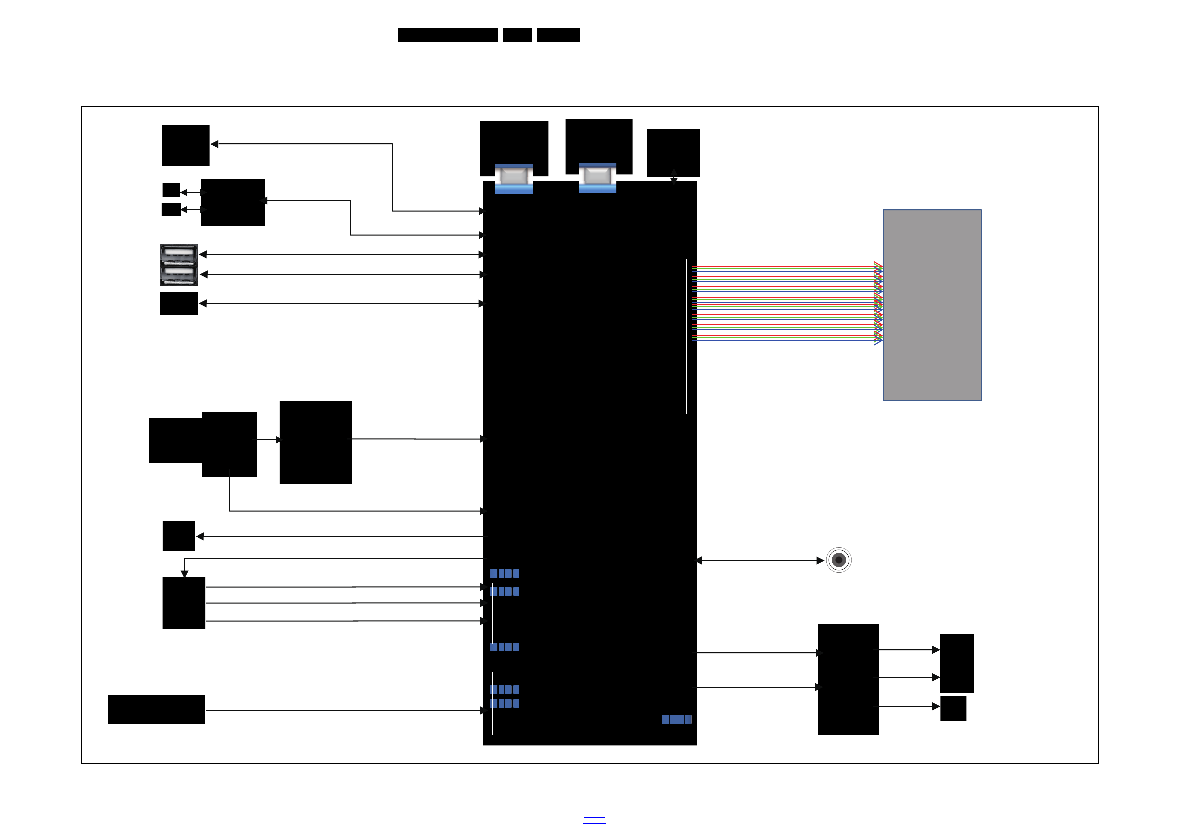
9. Block Diagrams
20170_400.eps
ADAC
GLUE
GLUE
GLUE
GLUE
GLUE
MT5593H
2x DDR 3
2x DDR 3
eMMC
TS
input
USB 3.0
USB 2. 0
USB 2. 0
USB 2. 0
Ethernet
HD M I Rx
LVDS/Vx1
Transmitter
SPI
ADAC
Analog
I/O
CVBS
Wi-Fi/BT
IF
Optical
HDMI Port 1 + MHL 2.0
DVB
-
T/C
Demodulator
Hybrid
Tuner
Audio
AMP
UHD
Panel
SPDIF
HDMI ARC
SERV.U
I2S
Analog L/R
9.1 Block diagram series
Block Diagrams
EN 35QM16.1L LA 9.
L
2016-Jul-08
back to
div.table
Page 36
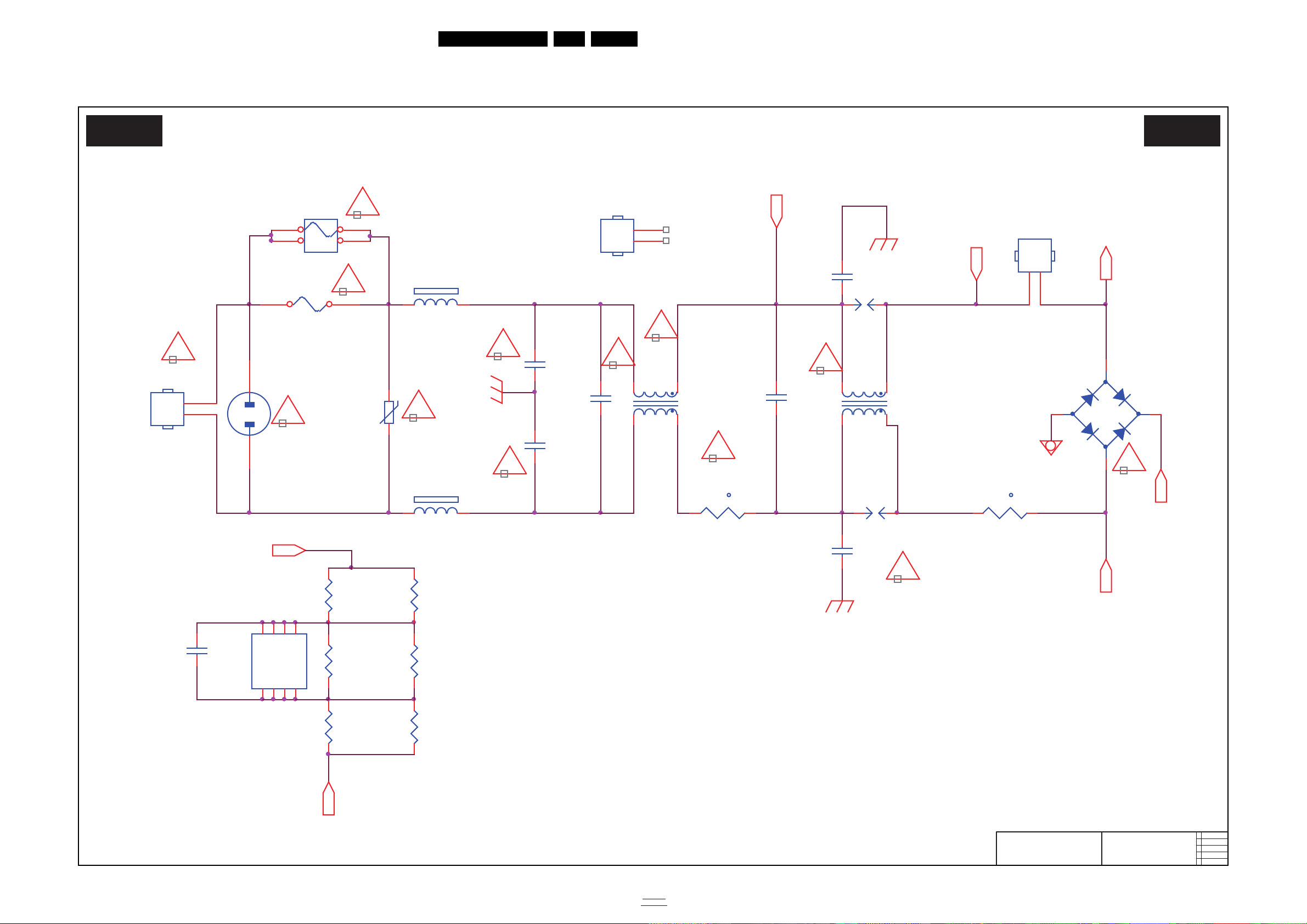
Circuit Diagrams and PWB Layouts
20030_549.eps
AC input
A01 A01
2015-11-30
3
715G7857
AC input
L9901
12mH
1
2
4
3
L9902
12mH
1
2
4
3
U9901
CAP004DG-TL
NC
1
D12D1
3
NC
4
NC
5D26D27NC8
CN9901
AC 2P
12
t
NR9902
2R
1 2
HS9901
HEAT SINK
1
2
SG9901
NC/DSPL-501N-A21F
VXB
R9907
510K 1/4W
R9905
NC / 510K 1/ 4W
R9908
510K 1/4W
R9906
NC / 510K 1/ 4W
R9903
510K 1/4W
R9904
510K 1/4W
BR
C9901
NC / 47pF 250V
C9902
NC / 47pF 250V
VXC
VXA
VXA
VXB
C9907
47PF
F9901
FUSE
1 2
3 4
-
+
BD9901
TS10K80-02
2
1
3
4
CN9903
NC/CONN
L1N
2
C9905
470NF 275V
RV9901
680V
SG9902
NC/DSPL-501N-A21F
FB9901
BEAD
1 2
C9906
470NF 275V
CN9902
NC/CONN
1
2
Vsin
FB9902
BEAD
12
!
!
!
!
!
!
!
!
!
!
!
!
!
C9903
330PF 250V
C9904
330PF 250V
F9902
NC / 5A 250V
t
NR9901
2R
1 2
10. Circuit Diagrams and PWB Layouts
10.1 A 715G7374 PSU
10-1-1 AC input
EN 36QM16.1L LA 10.
2016-Jul-08
back to
div.table
Page 37
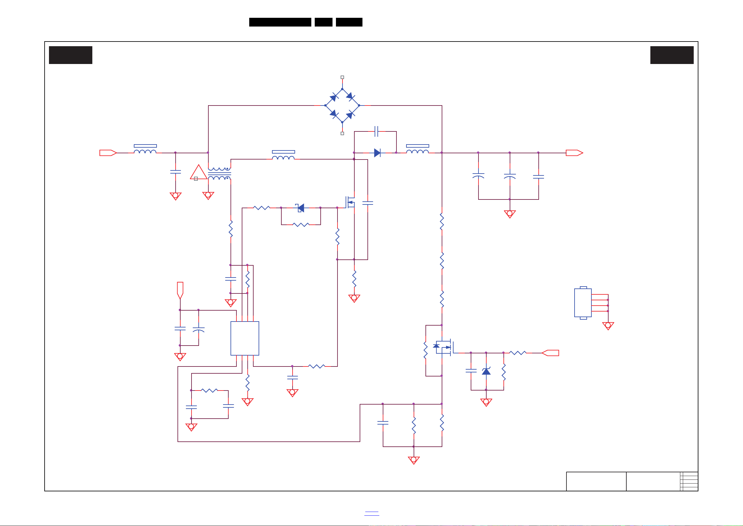
10-1-2 PFC
20030_550.eps
PFC
A02 A02
2015-11-23
715G7857
PFC
L9801
170uH
1 4
3 5
+
C9802
68UF 450V
+
C9803
68UF 450V
Q9802
BSS127
3
1
2
ZD9801
NC/SMF12A
1 2
R9809
24K 1/4W
FB9802
BEAD
1 2
R9815
470 OHM 1/4W
C9813
100N 50V
C9814
100N 50V
C9812
470NF 50V
R9812
47OHM
D9803
SS1060FL
12
R9803
1M 1% 1/4W
+
C9809
10UF 50V
R9804
NC/0R05
R9813
10K 1/8W
R9816
10K 1/8W 1%
C9811
1nF 50V
Q9801
TK18A60V
C9808
10PF 50V
R9811
10 OHM
R9807
10K 1/8W
C9806
NC/100PF
C9810
100N 50V
D9802
FMNS-1106S
R9817
100K 1/8W 1%
R9806
680K 1%
R9810
2K 1/8W 1%
R9802
1M 1% 1/4W
FB9891
BEAD
1 2
R9814
0.1R
C9801
1UF 450V
R9801
1M 1% 1/4W
C9815
470P 50V
HS9801
HEAT SINK
1
2
3
4
C9805
NC/47PF
U9801
LD7591T
INV1COMP2RAMP3CS
4
ZCD
5
GND
6
OUT7VCC
8
R9895
20K 1/8W 1%
C9804
NC
HV
Vsin
VCC_ON
!
VCC_ON
R9808
27K 1/8W 1%
FB9801
BEAD
12
-
+
BD9801
KBP206G X0G
2
1
3
4
Circuit Diagrams and PWB Layouts
EN 37QM16.1L LA 10.
2016-Jul-08
back to
div.table
Page 38
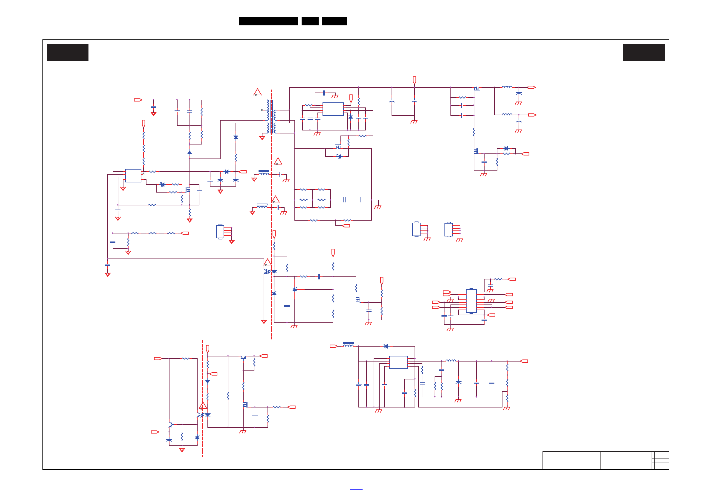
10-1-3 Standby
20030_551.eps
Standby
A03 A03
2015-11-23
715G7857
Standby
R9328
5.1K 1/4W
R9334
27 OHM 1/4W
D9313
SS1060FL
T9301
POWER X'FMR
1
2
4
5
6
7
8
10
11
Q9309
2N7002K
R9360
100 OHM 1/4W
R9313
3.3M 1/4W
C9352
100N 50V
R9315
3.3M 1/4W
C9355
2N2 50V
R9321
4R7
ZD9302
BZT52-B15
1 2
C9341
1uF 50V
R9362
10K 1/8W 1%
L9304
47uH
C9306
100N 50V
R9318
20K 1/8W
FB9302
BEAD
12
D9302
FR107G-A0
R9333
27 OHM 1/4W
Q9307
2N7002K
R9322
100KOHM 1/8W
R9363
1K5
C9340
NC/1uF
R9366
0R05
R9309
10R 1/8W 5%
L9302
3UH
C9315
220PF 250V
U9102
EL817M(X)
12
43
C9343
1N 50V
R9314
3.3M 1/ 4 W
R9317
3K
R9353
30R 1%
HS9301
HEAT SINK
1
2
3
4
C9333
100N 50V
C9358
1uF
R9326
510K 1/8W
C9353
1N 50V
R9331
27 OHM 1/4W
C9328
100N 50V
HS9302
HEAT SINK
1
2
3
4
R9354
30R 1%
R9364
10K OHM
C9342
1uF
C9308
330P 50V
C9303
NC/1NF
R9325
100 OHM 1/4W
CN9101
CONN
2
4
6
8
10
12
14
16
1
3
5
7
9
11
13
15
R9340
6.2K OHM 1/8W
Q9306
BTC4672M3
R9330
27 OHM 1/4W
D9312
SS1060FL
R9327
100K
C9302
2.2NF
L9303
3UH
D9314
1N4148W
R9365
2K 1%
C9351
1uF
R9332
27 OHM 1/4W
C9338
1N 50V
ZD9303
BZT52-B4V7_R1_00001
12
C9357
1uF
R9335
27 OHM 1/4W
Q9305
2N7002K
C9301
1NF
C9332
100N 50V
R9339
100K 1/8W
R9361
510K 1% 1/8W
ZD9301
BZT52-B16
1 2
R9338
100K 1%
C9335
47P 50V
R9337
0R05 1/4W
+
C9313
10UF 50V
+
C9305
10UF 50V
C9324
NC/1uF
C9325
100N
U9305
AOZ3015AI
PGND
1
VIN
2
AGND
3
VCC4FB
5
COMP
6
LX
7
EN
8
C9307
NC/47PF
R9345
1K 1/8W 1%
R9310
10K OHM 1/8W
R9329
8.2K 1/4W
C9329
100N 50V
HS9303
HEAT SINK
1
2
3
4
R9352
20K
R9320
33K 1/4W
C9354
2N2 50V
C9334
100P 50V
+12V_A
+3.5V/+5V
+12V_A
+12V
BL_ON/OFF
+3.5V/+5V
SYNC
+12V
12VS
SYNC
DV5
+VCC1
+12V_A
+12V
DIM
PS_ON
12VS
DV5
PS_ON
PS_ON
3D_ON
12VS
12VS
12VS
HV
VCC_ON
!
!
!
!
!
COLDHOT
D9304
SS1060FL
12
D9311
SK510C
12
R9306
39R 5%
C9330
1NF 500V
C9331
1NF 500V
Q9302
MTB15P04FP
Q9303
TK22A10N1
C9310
1NF
R9308
82 OHM
U9304
TL431G-AE2-R
BR
U9306
EL817M(X)
12
43
C9359
1uF 50V
+
C9320
2200uF 25V
+
C9321
2200uF 25V
D9301
SARS01-V1
FB9305
BEAD
1 2
R9302
330K 1/4W
R9303
330K 1/4W
R9305
82K 2W
R9304
0 OHM
R9301
330K 1/4W
R9316
100K 1/8W 1%
R9324
5K1 1/8W 1%
R9323
10ohm 1/4W +/ -1%
C9339
470NF 50V
R9351
3K
R9312
0.2R
R9311
1K 1/4W
R9346
3K3 1/8W 1%
R9347
1K OHM
R9341
9K1 1/8W 1%
R9342
2K2 1/8W 1%
R9343
1.5KOHM +-1%
U9302
SP6018ES8RGB
Timi ng
1
Pred
2
VR
3
Adj4GND
5
MOSG-C
6
Vdd
7
SYNC
8
R9348
39R 5%
FB9803
127R
1 2
Q9308
MMBT3906
C9818
680PF 250V
Q9301
TK11A65D
R9357
3K 1/8W +/-1%
BR
+VCC1
U9301
LD5532
BNO
1
COMP
2
CS
3
GND4OUT
5
VCC
6
NC
7
NC
8
+
C9326
470uF 25V
D9393
1N4148W
+
C9327
470uF 25V
R9356
0 OHM +-5%
C9336
4.7UF
R9355
11K 1/8W 1%
C9337
4.7UF
LED_OV
+
C9304
100UF 50V
R9307
2R7 1/4W
+
C9350
470uF 25V
+
C9356
470uF 25V
C9311
4.7nF 50V
Circuit Diagrams and PWB Layouts
EN 38QM16.1L LA 10.
2016-Jul-08
back to
div.table
Page 39
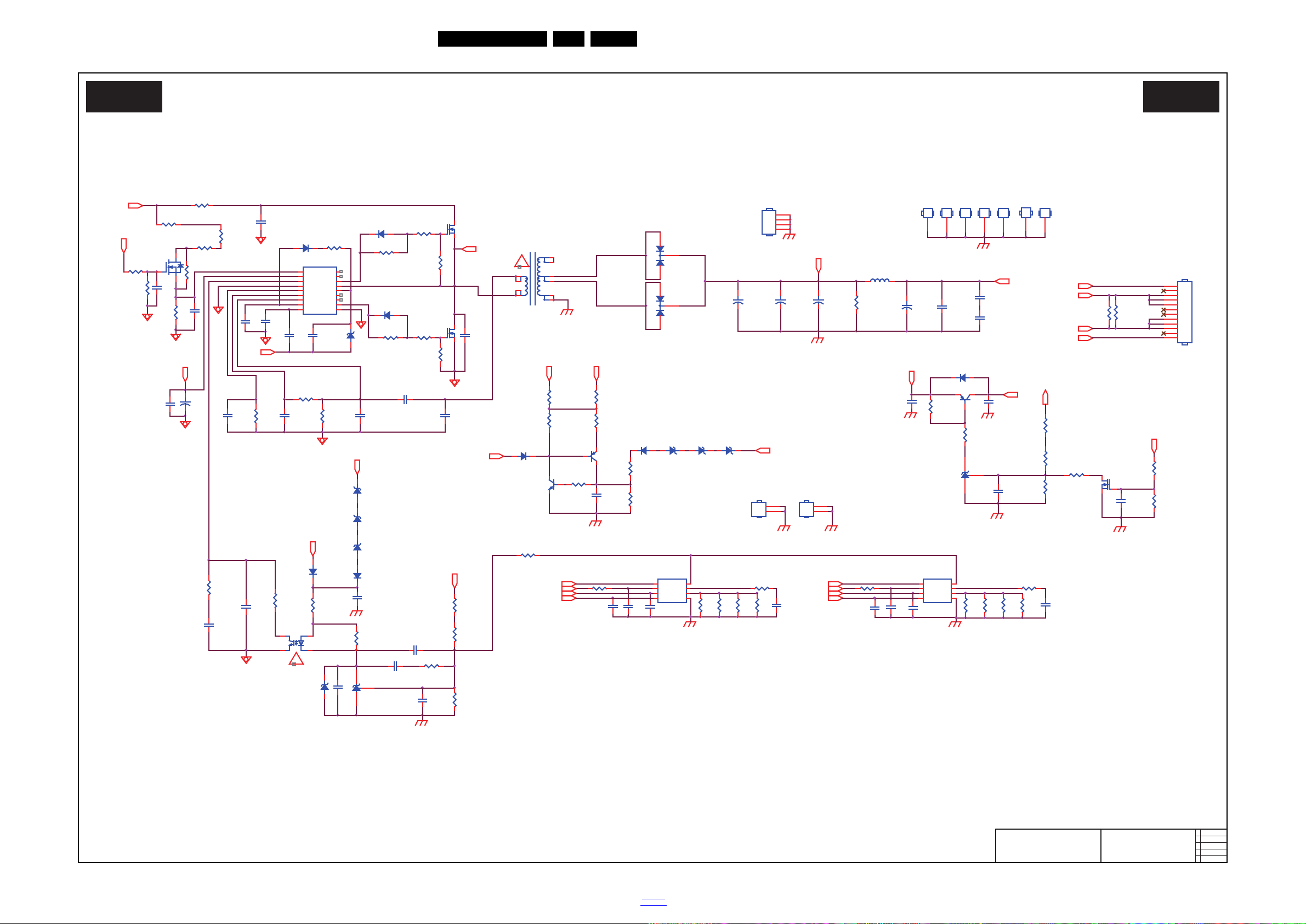
10-1-4 LED
20030_552.eps
LED
A04 A04
2015-11-23
715G7857
LED
U8102
EL817M(X)
1
23
4
ZD8107
BZT52-B9V1
1 2
R8107
10K OHM
R8106
NC/0R 05 1/ 4W
C8102
100N 50V
R8108
100K 1/8W
VCC_ON
Q8102
TK10A50D
Q8101
TK10A50D
C8146
100N 50V
R8172
10K 1/4W
R8160
0R05 1/4W
R8135
0R05 1/4W
U8106
TPV10 1D
DIM
1
EN
2
VCC
3
LED4GND
5
ISET
6
GM
7
COMP
8
C8135
1uF 50V
C8148
1uF
DIM
-VLED-1
IC_VCC
BL_ON/OFF
D8106
FMXA-2202S
1
2
3
Q8107
MMBT3906
D8107
FMXA-2202S
1
2
3
R8101
0.1R 1W
R8159
1.2R 1%
U8104
TL431G-AE2-R
R8154
1.2R 1%
R8129
NC/3K3 1/8W 5%
U8103
NC/TL431G-AE2-R
R8113
10R 1/8W 5%
R8158
1.2R 1%
R8111
10R 1/8W 5%
R8156
1.2R 1%
R8151
1.2R 1%
R8150
13 K
Q8106
MMBT3904
GND6
NC
1
GND7
GND
1
R8116
10R 1/8W
C8133
NC/470N F 50V
LED_OV
R8157
1.2R 1%
VLED
ZD8106
BZT52-B9V1
1 2
D8112
1N4148W
+
C8105
22UF 50V
C8141
100N 50V
R8128
NC/13K
R8171
10K 1/4W
R8155
0R05 1/4W
HS8105
HEAT SINK/NC
1
2
U8105
TPV101D
DIM
1
EN
2
VCC
3
LED4GND
5
ISET
6
GM
7
COMP
8
C8147
1uF 50V
C8143
1uF
DIM
-VLED-2
BL_ON/OFF
IC_VCC
C8140
NC/1NF 500V
C8111
5PF
D8108
0 OHN
R8153
1.2R 1%
C8136
1uF
+12V
C8157
NC/1uF
+VLED
R8126
NC/43K
R8127
NC/43K
Q8105
NC/2N 7002K
R8123
NC/1M 1/8W
R8124
NC/510K
IC_VCC
IC_VCC
U8101
SSC9522S
Vsen
1
Vcc
2
FB
3
GND
4
Css
5
OC
6
RC
7
Reg
8
RV9COM
10
VGL
11
NC
12
NC
13
VB
14
VS
15
VGH
16
NC
17
NC
18
ZD8101
BZT52-B15
1 2
C8137
NC
HS8102
HEAT SINK
1
2
3
4
C8116
100PF1KV
C8126
100N 50V
C8108
0.47UF 50V
C8113
560P 50V
D8101
SS1060FL
+
C8120
82uF 100V
D8103
UF4007
+
C8121
82uF 100V
+
C8122
82uF 100V
R8149
100K
ZD8109
BZT52-B30
1 2
C8115
NC/100PF
D8102
SS1060FL
C8106
10NF 50V
C8125
100N 50V
C8103
100N 50V
C8128
100N 50V
T8101
EE39
1
4
5
6
7
8
9
10
2
3
C8112
1uF
R8102
1M5 1/4W 1%
C8124
NC/1N F 500V
C8107
4.7uF 10V
L8101
3UH
HS8106
HEAT SINK/NC
1
2
C8127
NC/100P 50V
C8109
1UF
R8105
18K 1/8W
D8111
NC/SS1060FL
R8112
47 +-5%
R8114
10K 1/8W
R8117
10K 1/8W
C8104
100N 50V
C8131
100N 50V
C8110
47P 50V
R8115
47 +-5% 1/8W
R8120
NC
R8110
47K +-1% 1/4W
R8145
20K
C8101
1NF
VBoot
VBoot
+VLED
HV
VCC_ON
VLED
VLED
+12V
R8109
470 OHM 1/4W
!
R8103
1M5 1/4W 1%
R8140
47K
!
+VLED
CN8101
CONN
1
2
3
4
5
6
7
8
9
10
11
12
-VLED-1
+VLED
-VLED-2
+
C8123
82uF 100V
C8145
NC/1N F 500V
GND1
NC
1
R8104
1M5 1/4W 1%
ZD8104
BZT52-B18
1 2
ZD8105
BZT52-B20
1 2
R8132
1K 1/8W 1%
D8109
SS1060FL
R8133
NC/0R 05 1/ 4W
R8131
5.1KR 1%
R8136
2K 1/8W 1%
C8132
100N 50V
R8134
1K 1/8W 1%
+12V
VLED
DV5
C8117
27NF
R8118
200 OHM +/-1%
R8152
1.2R 1%
R8137
1K 1/8W 1%
R8139
1K 1/8W 1%
R8121
0R05 1/4W
R8122
0R05 1/4W
R8130
NC/510OHM
R8142
6.8K
D8110
1N4148W
C8129
NC
R8141
47K
R8138
1.5K OHM
R8119
470OHM
ZD8108
BZT52-B7V5
1 2
Q8103
BSS127
3
1
2
C8114
1N 50V
R8125
NC/36K
C8134
NC/1uF
ZD8102
BZT52-B18
1 2
GND3
GND
1
GND2
NC
1
GND5
NC
1
GND4
GND
1
Q8104
NC/MMBT3906
Circuit Diagrams and PWB Layouts
EN 39QM16.1L LA 10.
2016-Jul-08
back to
div.table
Page 40
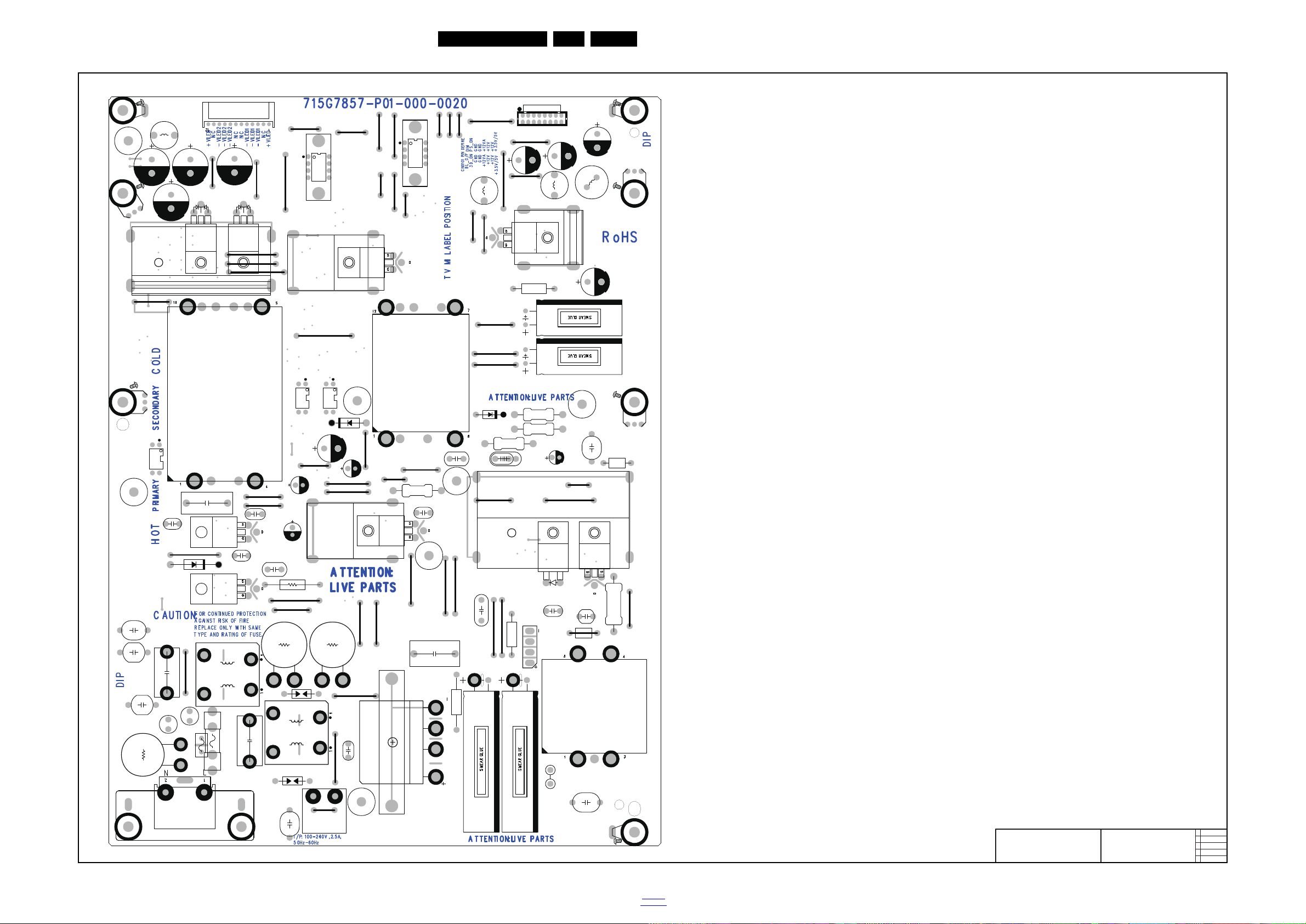
10-1-5 Power layout top
20030_553.eps
2015-11-18
715G7857
LAYOUT TOP
C8105
C9307
C9313
C9805
C9907
D9302
U8102
U9102
U9306
R9312
R9305
J955
J952
J938
J939
SU1
SU2
SU4
J935
J928
J920
SU6
J931
J950
J942
J930
C8120
C9305
J932
J934
C9803
C9806
C9809
J921
J923
C8101
J940
J944
J933
J941
J949
J943
J936
SU7
J948
J947
J911
F9902
SU5
J937
C8111
J954
J953
J929
SU8
J946
T8101
T9301
D9301
J914
J910
J907
J912
J913
J916
J904
J901
J915
J917
J922
J925
J909
J903
J902
J908
J906
J905
J919
J926
J927
J918
J924
J945
R9348
R9306
H1
S6
J951
MH8
MH9
MH10
C8116
C8115
C9303
C9301
C9315
CN9902
CN9903
D8106D8107
D9802
FB9803
FB9302
HS9302
L8101
L9302
L9303
L9304
NR9901 NR9902
R9814
CN9101
C9302
MH3
SG9901
SG9902
D8103
MH2
MH1
C9905
C9906
RV9901
F9901
U8106
U8105
MH4
HS8105
HS8106
MH5
Q9301
HS8102
C8121
C8122
R8101
C9801
C9802
C9350
C9304
C9326
C9327
C9356
MH6
MH7
C9804
FB9802
FB9891
HS9901
HS9801
BD9901
FB9901
FB9902
Q8102
Q8101
C8123
CN8101
BD9801
L9901
L9902
C8117
HS9301
C9818
C9901
C9902
C9903
C9904
C9320
C9321
HS9303
Q9302
FB9305
FB9801
L9801
CN9901
GND1
GND2
GND5
GND6
Q9801
Q9303
GND3
GND4
GND7
Circuit Diagrams and PWB Layouts
EN 40QM16.1L LA 10.
2016-Jul-08
back to
div.table
Page 41
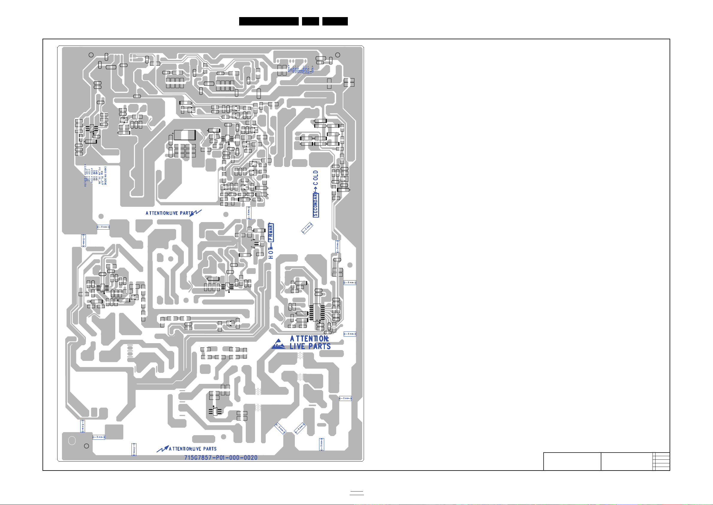
10-1-6 Power layout bottom
20030_554.eps
2015-11-18
715G7857
LAYOUT BOTTOM
C8103
C8109
C8112
C8104
C8108
C8113
C8114
C8106
C8107
C8125
C8126
C8124
C8110
C8132
C9308
C9311
C9340
C9343
C9325
C9324
C9339
C9329
C9337
C9358
C9357
C9354
C9351
C9352
C9353
C9332
C9334
C9333
C9335
C9336
C9355
C9306
C9338
C9342
C9310
C9810
C9808
C9812
C9811
C9814
U9901
R8102
R8103
R8113
R8111
R8112
R8104
R8114
R8105
R8115
R8116
R8117
R8119
R8120
R8118
R8109
R8136
R8134
R9813
R9311
R9309
R9308
R9310
R9307
R9313
R9314
R9343
R9345
R9328
R9321
R9315
R9338
R9339
R9334
R9333
R9335
R9352
R9356
R9351
R9357
R9322
R9325
R9326
R9317
R9318
R9362
R9361
R9801
R9806
R9802
R8121
R9809
R9810
R9895
R9816
R9817
R9904
R9903
R9905
R9906
R9907
R9908
RJ905
R8110
R9316
R9803
R9364
R9340
R9365
R9360
RJ907
FID7
FID6
C9341
R8132
R9327
R9320
R9366
C8127
C8128
C8148
C8146
C8135
C8137
C8147
C8131
C8145
C8141
C8143
R8149
R8154
R8138
R8141
R8172
R8145
R8152
R8151
R8153
R8142
R8171
R8159
R8158
R8156
R8157
R8130
R8129
FID5
R8160
R8155
R8128
C8102
C8136
C8157
C8134
C8133
C9813
R8108
R8125
R8123
R8124
R9808
R9807
R8106
R8139
R9812
R8137
R8107
C8140
R9329
R9347
R9346
R9341
R9363
R8135
R8133
R9353
R9354
R8127
R8126
R9304
R9301R9302
R9303
C9815
R8122
R9804
R9815
R9811
Q8104
Q8106
Q8107
Q9308
Q8103
Q8105
Q9305
Q9309
Q9307
Q9802
RJ904
RJ906
R8131
R9330
R9331
R9332
C9328
RJ901
RJ902
U8103
U8104
U9304
R8150
R8140
C8129
U9305
U9302
U9801
U9301
C9330C9331
R9324
C9359
R9355
R9323
R9337
R9342
RJ903
C9360
S2
S1
S4
S3
U8101
D9311
Q9306
D8101
D8102
D8108
D8109
D8110
D8111 D8112
D9304
D9312
D9313
D9314
D9393
D9803
ZD8101
ZD8102
ZD8104
ZD8105
ZD8106
ZD8107
ZD8108
ZD8109
ZD9301
ZD9302
ZD9303
ZD9801
Circuit Diagrams and PWB Layouts
EN 41QM16.1L LA 10.
2016-Jul-08
back to
div.table
Page 42
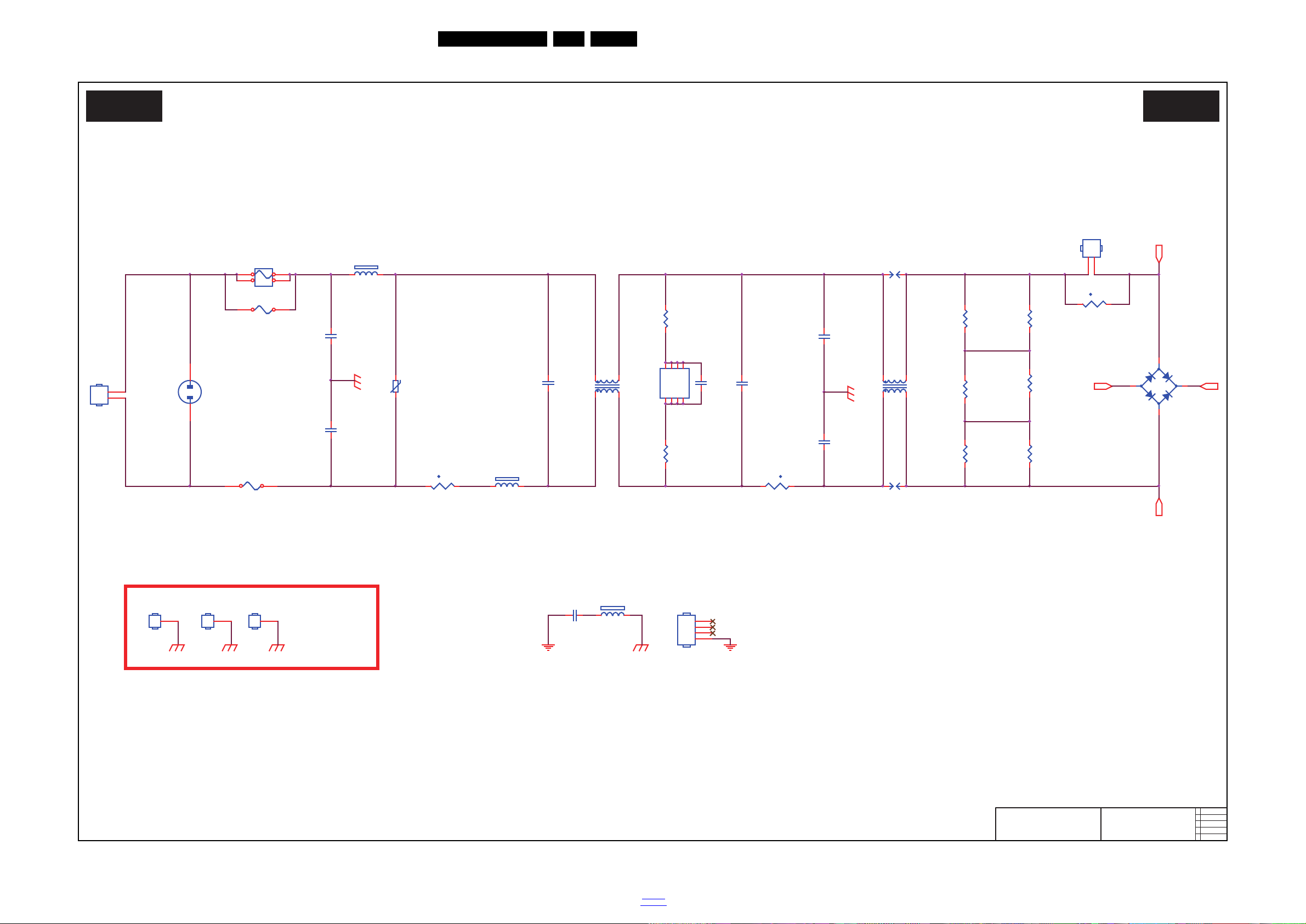
10.2 A 715G6973 PSU
19900_508.eps
AC Input
A01 A01
2015-02-11
715G6973
AC Input
CN9901
NC/CONN
1
2
CN9902
AC SOKET
12
F9901
1 2
3 4
RV9901
680V
FB9902
BEAD
12
FB9901
BEAD
12
C9901
470NF 275V
C9902
470NF 275V
L9901
12mH
1
2
4
3
R-
-
+
BD9901
GBJ1008-FUC
2
1
3
4
BO
C9911
47pF 250V
N
Vsin
C9916
1NF 250V
U9901
CAP004DG-TL
NC
1
D12D1
3
NC
4
NC5D26D27NC
8
C9907
47PF
R9901
510k 1/2W
R9902
510k 1/2W
GND4
GND
1
CN9903
NC / CONN
L1N
2
GND2
GND
1
GND1
GND
1
T5AH/250V
NC
NC
FB9903
BEAD
1 2
C9913
220PF 250V
C9912
47pF 250V
t
NR9903
1R
12
C9914
220PF 250V
t
NR9902
1R
1 2
L9902
12mH
1
2
4
3
SG9901
NC/DSPL-501N-A21F
SG9902
NC/DSPL-501N-A21F
F9902
R9903
NC/ 510K 1/ 4W
R9904
NC/ 510K 1/ 4W
R9905
NC/ 510K 1/ 4W
F9903
R9906
NC/ 510K 1/ 4W
R9907
NC/ 510K 1/ 4W
R9908
NC/ 510K 1/ 4W
t
NR9901
1R
12
HS9901
HEAT SINK
1
2
3
4
10-2-1 AC Input
Circuit Diagrams and PWB Layouts
EN 42QM16.1L LA 10.
2016-Jul-08
back to
div.table
Page 43
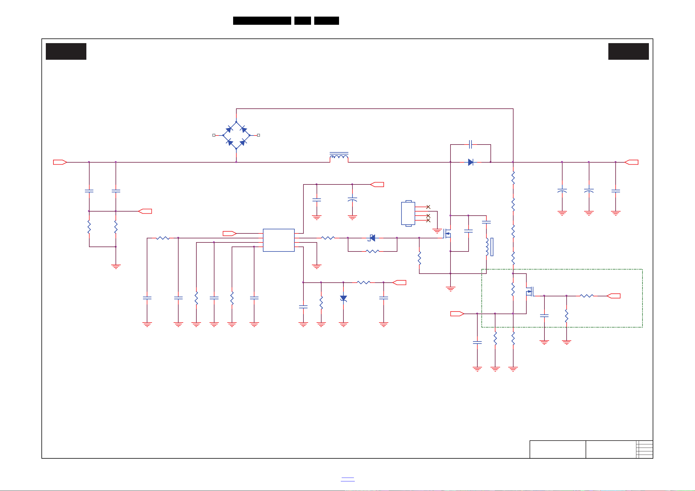
10-2-2 PFC
19900_509.eps
PFC
A02 A02
2015-02-11
715G6973
PFC
-
+
BD9801
KBP208G-C
2
1
3
4
Q9801
TK18A60V
R9816
10K 1/8W 1%
C9815
NC/47PF
D9802
SS1060
12
R9815
33R 1%
C9813
3.3nF 50V
R9813
NC / 24K 1/ 8W 1%
ZD9801
BZT52-B3V6
12
R9817
10K 1/8W 1%
R9812
47R 1%
C9812
47PF 50V
HS9801
HEAT SINK
1
2
3
4
R-
+VCC2
+
C9810
10UF 50V
C9811
100N 50V
C9805
1NF 50V
R9808
16K +-1% 1/8W
R9807
470K 1%
C9807
0.47uF 50V
R9809
27K 1/8W 1%
C9806
1uF
R9810
22K 1/8W 1%
C9808
10N 50V
R9811
33K 1/8W 1%
C9809
10N 50V
R9818
10K 1/8W 1%
C9818
47PF
C9817
100N 50V
FB9904
BEAD
12
L9801
220uH
6
4
C9816
1NF
C9814
47PF
D9801
FMNS-1106S
+
C9801
82uF 450V
+
C9802
82uF 450V
Vbus
R9803
1MOHM +-1% 1/4W
R9805
680K OHM +-1% 1/4W
R9806
100K 1%
R9804
680K OHM +-1% 1/4W
FB_PFC
FB_PFC
+VCC2
U9801
SSC-2005S
FB
1
COMP
2
RT
3
RDLY4CS
5
GND
6
OUT
7
VCC
8
R9819
NC/0R05
Q9802
AO3160
R9814
10R 1/ 8W 5%
Vsin
C9803
1UF 450V
C9804
1UF 450V
R-
R9801
0.1R 3W
R9802
0.1R 3W
Circuit Diagrams and PWB Layouts
EN 43QM16.1L LA 10.
2016-Jul-08
back to
div.table
Page 44
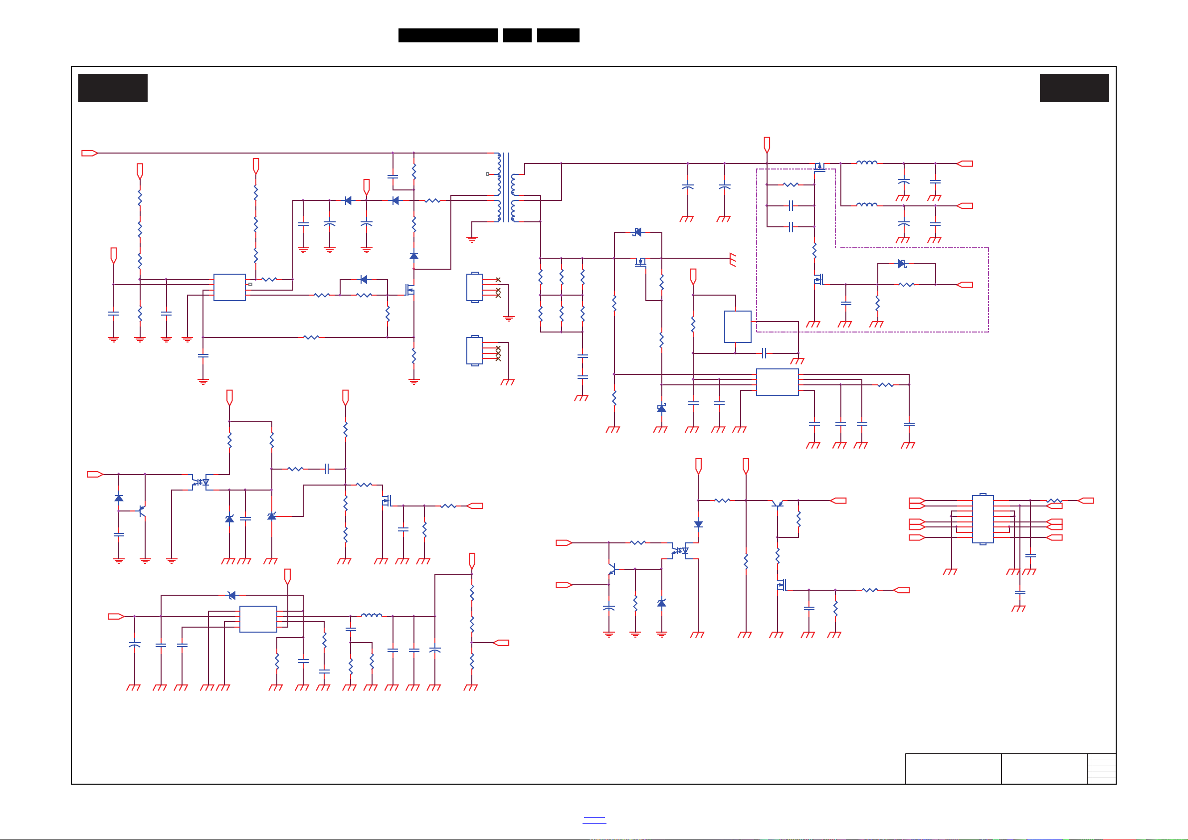
10-2-3 Main power
19900_510.eps
Main power
A03 A03
2015-02-11
715G6973
Main power
C9303
0.1uF 50V
R9122
1K5 +-1% 1/8W
R9109
10K 1/8W 1%
R9146
0R05
12VS
R9123
4.7K 1/8W
C9118
NC/1uF
U9103
AS431AN-E1
+VCC1
R9131
3K
D9108
1N4148
Q9106
BTC4672M3
C9304
1nF 50V
+
C9121
10UF 50V
R9301
3K 1/8W +/-1%
R9124
1K 1/8W 1%
+
C9132
10UF 50V
+3.5V
C9119
220N 50V
C9106
2.2NF
L9301
47uH
+VCC2
NC
+12V
R9126
2K2 1/8W 1%
R9127
1K5 +-1% 1/8W
Q9109
NC/MMBT3906
12VS
R9132
100KOHM +-1% 1/4W
+12V_A
R9125
9K1 1/8W 1%
R9150
22R 5%
DV5
D9107
NC/1N4148W
12VS
R9128
6.2K 1%
Q9105
2N7002K
Q9102
AOTF298L
ZD9105
BZT52-B15
1 2
Vbus
C9120
0.1uF 50V
U9105
SP6018ES8RGB
Timing
1
Pred
2
VR
3
Adj
4
GND
5
MOSG-C
6
Vdd
7
SYNC
8
R9129
10K OHM +-5% 1/8W
R9130
330K 1/8W 5%
C9130
NC/4.7NF 50V
U9106
NC/AS78L12RTR-G1
IN
3
OUT
1
GND
2
D9104
SK810C
12
DV5
C9133
10N 50V
+
C9109
1500UF 35V
+
C9110
1500UF 35V
+
C9105
100UF 50V
R9111
82K 2W
R9302
20K 1/8W 1%
C9305
2.2nF 50V
FB_SB
C9306
2.2nF 50V
D9106
1N4148W
R9133
2K 1/8W 1%
R9303
30 OHM 1/ 4W
R9304
30 OHM 1/ 4W
R9134
10K 1/8W 1%
D9103
FR107G-A0
BO BO
Q9107
MMBT3906
R9135
10K 1/8W 1%
R9136
10K 1/8W 1%
R9118
100K 1/8W 1%
D9101
1N4148W
R9142
10ohm +/-1% 1/8W
Q9103
AOD4185
Q9108
2N7002K
R9106
82 OHM
T9101
POWER X'FMR
1
2
4
5
6
7
8
10
11
C9307
1uF
C9308
1uF
+
C9309
470UF 25V
C9122
0.1uF 50V
R9105
10ohm +/-1% 1/8W
C9112
NC/1uF
C9111
NC/1uF
R9137
100 OHM 1/4W
R9138
510K 1% 1/8W
PS_ON
R9101
0.2R
12VS
R9305
11K 1/8W 1%
DV5LED_OVP
R9306
0R051/8W
Q9104
2N7002K
R9107
1Kohm +-1% 1/4W
R9307
3K 1/8W +/-1%
R9119
100K 1/8W 1%
R9112
27 OHM
R9113
27 OHM
R9114
27 OHM
R9115
27 OHM
C9103
330P 50V
R9116
27 OHM
R9117
27 OHM
C9117
0.1uF 50V
C9104
0.1uF 50V
R9121
510K 1% 1/8W
U9301
AOZ3015AI
PGND
1
VIN
2
AGND
3
VCC4FB
5
COMP
6
LX
7
EN
8
R9120
100 OHM 1%
ZD9103
SS1060
1 2
+3.5V
C9107
2N2 50V
R9110
2R2 +-5% 1/4W
R9139
8.2K 1/4W
R9140
5K1 1/8W 1%
U9101
LD5532
BNO
1
COMP
2
CS
3
GND4OUT
5
VCC
6
NC
7
NC
8
+12V
HS9101
HEAT SINK
1
2
3
4
D9102
FR107G-A0
+12V_A
PS_ON
HS9102
HEAT SINK
1
2
3
4
+3.5V
C9114
1uF
C9116
1uF
Q9101
TK11A65D
FB_SB
DIMBL_ON/OFF
3D_ON
R9141
5K1 1/8W 1%
R9145
0R05 1/4W
CN9101
CONN
2
4
6
8
10
12
14
16
1
3
5
7
9
11
13
15
R9143
4R7 1/4W 5%
C9108
2N2 50V
L9101
3UH
L9102
3UH
C9124
1uF
C9123
1uF
+
C9113
470UF 25V
+
C9115
470UF 25V
U9102
EL817M(X)
1
23
4
C9102
1000pF 50V
D9105
SS1060
1 2
C9101
4N7 50V
C9125
47P 50V
12VS
FB_12V
FB_12V
C9126
0.1uF 50V
+
C9301
470uF 25V
C9127
100PF 50V
12VS
C9128
0.1uF 50V
R9144
47K +-1% 1/4W
+12V
+12V_A
R9104
100K 1/8W 1%
ZD9301
BZT52-B4V7
12
+VCC1
C9131
NC/ 100N 50V
U9104
EL817M(X)
1
23
4
C9302
1uF
C9129
1NF 500V
R9147
330K +-1% 1/4W
R9149
330K +-1% 1/4W
ZD9104
BZT52-B15
1 2
R9148
330K +-1% 1/4W
R9103
3.3M 1/ 4W
R9102
3.3M 1/4W
R9108
3.3M 1/ 4W
Circuit Diagrams and PWB Layouts
EN 44QM16.1L LA 10.
2016-Jul-08
back to
div.table
Page 45
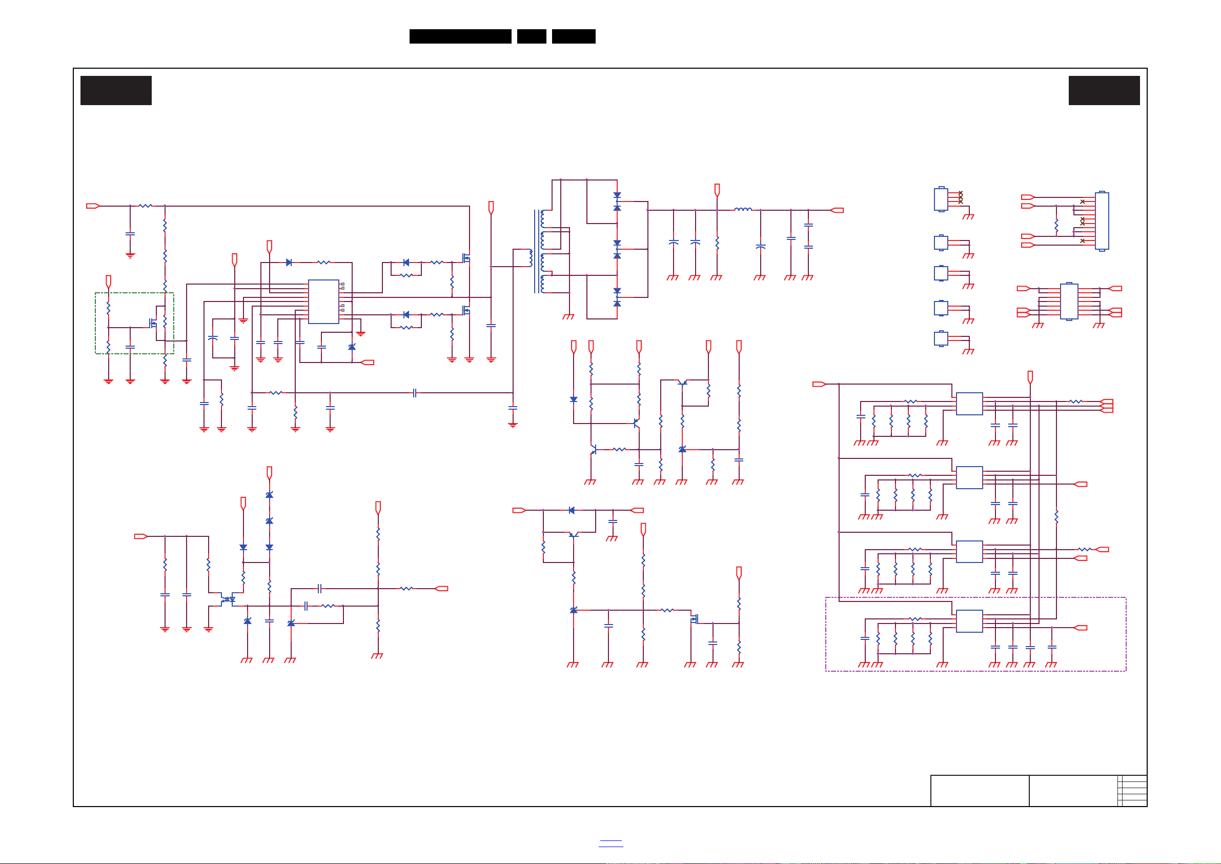
10-2-4 LED Driver
19900_511.eps
LED Driver
A04 A04
2015-02-11
715G6973
LED Driver
R8143
1.5R
R8144
1.5R
+VLED
U8105
TPV101D
DIM
1
EN
2
VCC
3
LED
4
GND
5
ISET
6
GM
7
COMP
8
LED_OVP +12VDV5
U8106
TPV101D
DIM
1
EN
2
VCC
3
LED
4
GND
5
ISET
6
GM
7
COMP
8
D8108
SS1060FL
+VCC2
Q8103
MMBT3904
R8141
1.5R
R8142
1.5R
R8126
0 OHM +-5% 1/8W
R8124
75 KOHM +-1% 1/8W
R8129
NC / 0 OHM +-5% 1/8W
HS8101
HEAT SINK
1
2
3
4
R8127
2K 1/8W 1%
R8130
1K 1/8W 1%
R8146
1.5R
R8128
1K 1/8W 1%
R8145
1.5R
-VLED1
C8105
0.47UF 50V
Q8104
MMBT3906
R8106
NC
R8151
0 OHM +-5% 1/8W
C8136
1uF
+VCC2
R8107
470R 1/8W 1%
C8106
560PF 50V
R8108
180R 1%
-VLED1
-VLED2
-VLED1
-VLED2
C8107
1nF 50V
C8110
1uF
C8125
0.1uF 50V
C8111
47P 50V
+12V
R8159
5K1 1/8W 1%
Q8105
MMBT3906
R8152
0 OHM +-5% 1/8W
R8147
1R 1%
C8137
1uF
R8148
1R 1%
R8131
1K 1/8W 1%
+12V
R8132
5K1 1/8W 1%
U8104
AS431AN-E1
TPV101_VCC
3D_ON
R8160
62K 1/8W 1%
R8133
30K 1/8W 1%
DIM
R8134
4.3K OHM 1%
C8126
0.1uF 50V
BL_ON/OFF
C8133
1uF
C8112
5PF
VLED1
C8109
27NF
VLED1
HS8102
HEAT SINK
1
2
HS8103
HEAT SINK
1
2
ZD8101
BZT52-B15
1 2
D8106
SS1060FL
+12V
VS
D8107
SS1060FL
R8119
4.3K OHM 1%
ZD8103
BZT52-B16
1 2
VLED1
R8149
1.5R
R8150
1.5R
R8153
0 OHM +-5% 1/8W
U8107
TPV101D
DIM
1
EN
2
VCC
3
LED
4
GND
5
ISET
6
GM
7
COMP
8
C8132
1uF
C8131
0.1uF 50V
C8138
1uF
R8154
0 OHM +-5% 1/8W
U8108
TPV101D
DIM
1
EN
2
VCC
3
LED
4
GND
5
ISET
6
GM
7
COMP
8
R8163
10K 1/8W 1%
C8135
1uF
C8113
100PF
C8134
0.1uF 50V
D8101
UF4007
R8164
1K 1/8W 1%
R8109
10ohm +/-1% 1/8W
C8139
1uF
FB_LED
C8141
100PF 50V
D8102
SS1060FL
D8103
SS1060FL
R8110
10ohm +/-1% 1/8W
R8113
10ohm +/-1% 1/8W
ZD8104
BZT52-B30
1 2
R8111
47R 1%
R8114
47R 1%
R8112
10K 1/8W 1%
R8115
10K 1/8W 1%
U8103
AS431AN-E1
C8124
NC/0. 47U F 50V
FB_LED
FB_LLC
FB_LLC
R8120
NC/3K 1/8W 5%
VS
R8166
3K3 1/8W 1%
Q8107
LMBT3906LT1G
1
2 3
+12V
TPV101_VCC
R8165
510 OHM +-1% 1/8W
D8110
1N4148W
TPV101_VCC
U8109
AS431AN-E1
R8172
510K 1% 1/8W
Q8108
2N7002K
C8143
0.47UF 50V
R8171
1 MOHM +-1% 1/8W
C8108
100PF1KV
BL_ON/OFF
DIM
R8167
47K 1/8W 1%
R8155
10K 1/4W
R8168
43K 1/8W 1%
R8169
9K1 1/8W 1%
R8157
10K 1/4W
T8101
POWER X'FMR
1
4
5
6
7
8
9
10
11
12
3D_ON
C8122
NC
C8145
1uF
R8170
47K 1/8W 1%
C8123
0.1uF 50V
C8127
0.1uF 50V
HS8105
HEAT SINK
1
2
HS8104
HEAT SINK
1
2
C8128
1uF
R8125
470K +-5% 1/8W
CN9102
NC/CONN
2
4
6
8
10
12
14
1
3
5
7
9
11
13
C8101
1NF
Vbus
R8101
0.1R
C8144
1uF
D8104
FMX-23S
1
2
3
D8105
FMX-23S
1
2
3
U8101
SSC9522S
Vsen
1
Vcc
2
FB
3
GND
4
Css
5
OC
6
RC
7
Reg
8
RV9COM
10
VGL
11
NC
12
NC
13
VB
14
VS
15
VGH
16
NC
17
NC
18
+VLED
C8129
0.1uF 50V
C8130
1uF
+VLED
Q8101
TK10A50D
+VLED
+VLED
Q8102
TK10A50D
+
C8116
220UF 100V
+
C8117
220UF 100V
R8103
1M5 1/4W 1%
R8104
1M5 1/4W 1%
R8102
1M5 1/4W 1%
R8118
75K
C8140
1NF 500V
D8109
FMX-23S
1
2
3
R8161
NC/0R05
C8142
100N 50V
For Power Saving
Q8106
AO3160
R8162
10K 1/8W 1%
CN8101
CONN
1
2
3
4
5
6
7
8
9
10
11
12
L8101
3UH
R8105
18K 1/8W 1%
+
C8118
39uF 160V
C8102
0.1uF 50V
R8123
100K 1/8W 1%
ZD8102
BZT52-B16
1 2
NC
-VLED2
C8104
0.1uF 50V
R8158
0R05 1/4W
+
C8103
22UF 50V
R8135
1.5R
R8136
1.5R
C8119
1NF 500V
R8156
NC/0 OHM +-5% 1/8W
C8120
0.1uF 50V
C8121
0.1uF 50V
R8139
1.5R
R8140
1.5R
VLED1
R8137
1.5R
R8138
1.5R
U8102
EL817M(X)
1
23
4
R8117
470R 1%
C8115
10N 50V
R8116
2K43 1/8W 1%
R8121
750K 1%
R8122
150K 1/8W +/-1%
VLED1
C8114
4.7uF 10V
Circuit Diagrams and PWB Layouts
EN 45QM16.1L LA 10.
2016-Jul-08
back to
div.table
Page 46
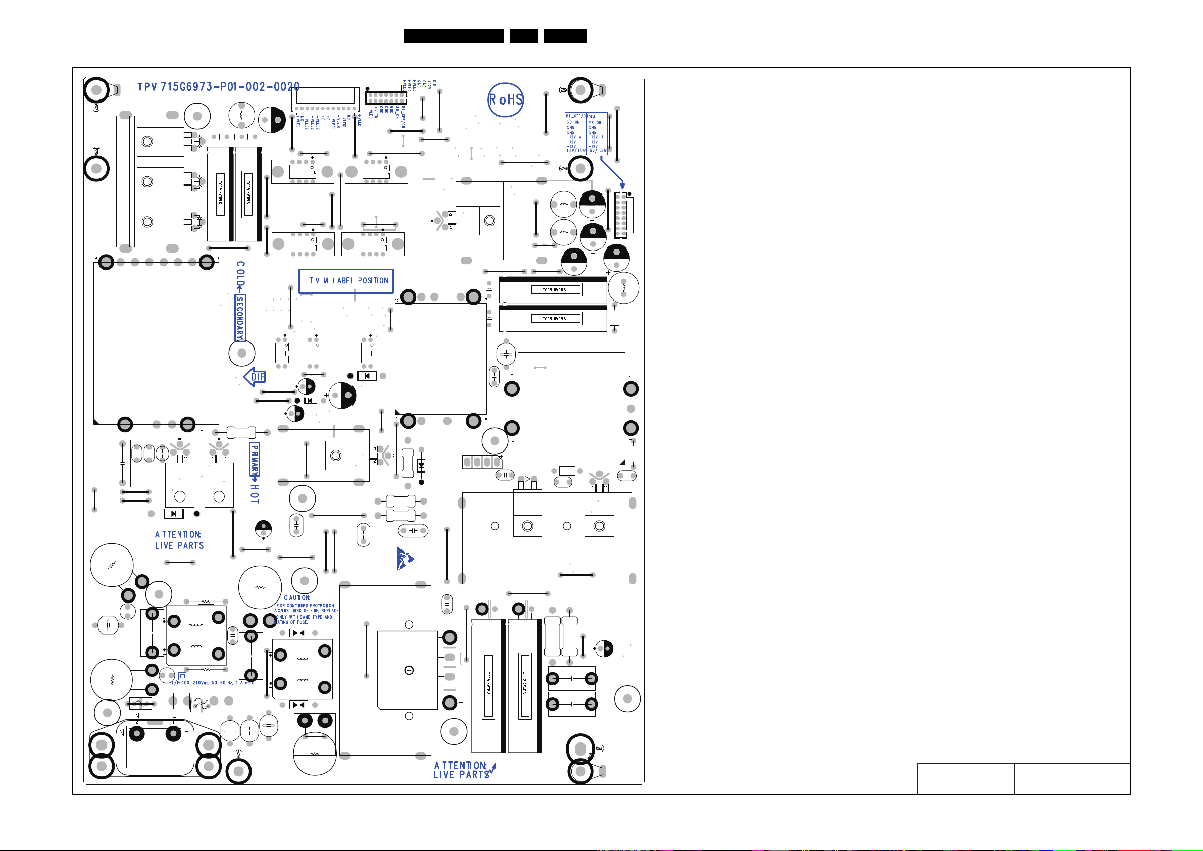
10-2-5 Power layout top
19820_548.eps
2014-12-02
715G6973
LAYOUT TOP
C9121
C8103
C9810
C9814
C9815
C9907
D9102
U8102
U9104
R9111
T8101
J9901
J9902
J9801
J9103
J9105
J9111
J9101
J8105
J8104
J9108
J9802
J8120
J9104
J9116
J9803
J9804
J8101
J9117
J9118
J8107
J9903
J8111
J9114
J9106
J9109
J9115
J9301
F9902
F9903
J9113
C9132
J9107
D9108
R9150
J8114
J8116
J8119
J8122
J8124
J8113
J9112
J9904
J9102
J8123
J8103
J8102
J8117
J8115
J8112
J8108
J8106
J8121
J9805
J9905
C9105
SU2
SU3
SU4
SU9
SU1
SU8
SU7
SU6
SU5
C9818
C9819
C9820
J8109
J9119
C9106
C9109
C9110
C9309
D9103
F9901
R9901
R9902
U9102
C9301
R9101
T9101
DR1
DR2
DE4
DR7
DR6DR5
DR8
DR3
C8112
C8108
C8118
C9113
C9115
C8101
C9802
C9801
C9816
C9803
C9804
C9901
C9902
C9913
CN8101
CN9901
CN9903
D9801
FB9901
FB9902
HS8102
HS8103
U8105
U8106
L8101
L9101
L9102
L9301
R9801
R9802
RV9901
SG9901
SG9902
D8105
D8104
HS8101
HS9901
BD9901
D8101
CN9102
GND1
GND2
GND4
C8116
C8117
MH7
MH2
MH4
MH3
MH1
MH6
MH5
CN9101
C9914
HS9801
HS9101
HS9102
HS8104
HS8105
U8107 U8108
C9916
D8109
NR9901
NR9902
NR9903
L9801
C8109
R8101
CN9902
FB9904
FB9903
BD9801
FB9801
C9911
C9912
C8113
L9901
L9902
Q8102 Q8101
Q9101
Q9102
Q9801
Circuit Diagrams and PWB Layouts
EN 46QM16.1L LA 10.
2016-Jul-08
back to
div.table
Page 47
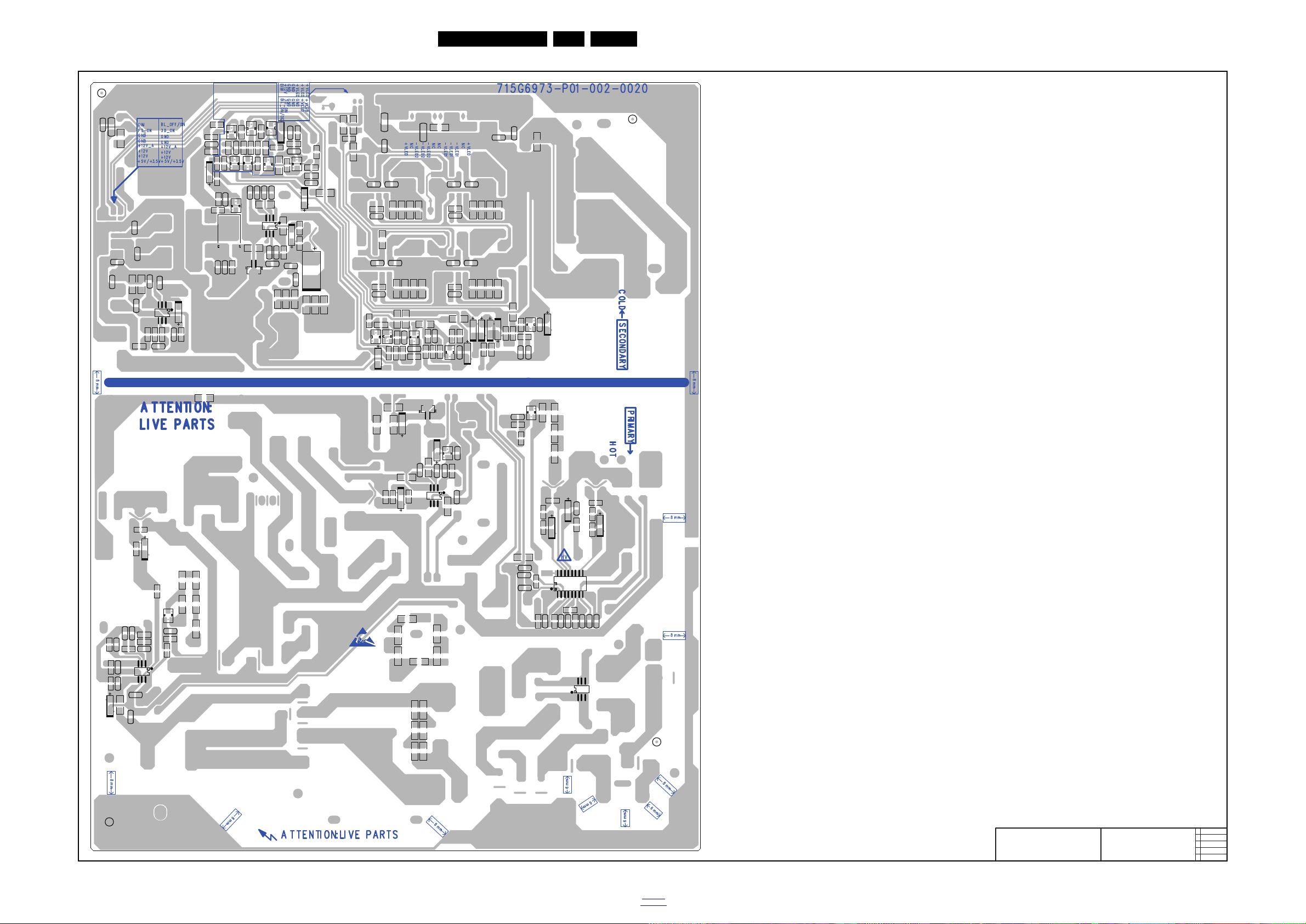
Circuit Diagrams and PWB Layouts
19820_549.eps
2014-12-02
715G6973
LAYOUT BOTTOM
C8102
C8110
C8133
C8104
C8105
C8106
C8107
C8115
C8122
C8114
C8123
C8136
C8127 C8128
C8124
C8141
C8137
C8129 C8130
C8120
C8121
C8140
C8119
C8111
C8125
C8126
C9103
C9101
C9118
C9112
C9111
C9119
C9117
C9124
C9308
C9307
C9305
C9302
C9303
C9304
C9128
C9127
C9126
C9125
C9123
C9306
C9107
C9108
C9104
C9120
C9114
C9116
C9122
C9102
C9809
C9808
C9811
C9813
C9812
C9807
C9806
C9805
U9901
R8103 R8104
R8110
R8102
R8112
R8118
R8105
R8113
R8115
R8107
R8106
R8108
R8117
R8116
R8151
R8125
R8138
R8137
R8135
R8136
R8152
R8139
R8140
R8141
R8142
R8155
R8157
R8156
R8129
R8127
R8130
R8131
R8134
R9146
R9109
R9113
R9114
R9112
R9110
R9126
R9127
R9123
R9122
R9125
R9124
R9139
R9144
R9143
R9130
R9115
R9117
R9116
R9302
R9306
R9301
R9307
R9305
R9118
R9119
R9121
R9303
R9304
R9131
R9136
R9138
R9103R9102
R9108
R9815
R9803
R9814
R9816
R9804
R9808
R9805
R9812
R9813
R9810
R9809
R9811
R9806
R9807
R9908
R9905
R9904
R9907
R9903
R9906
SM9
R9132
R8114
SM12
SM13
U9105
U9801
U9301
R9104
R8111
R9106
JR9101
R8109
R8147
R8148
R8149
R8150
C8139
R8154
R8146
R8145
R8143
R8144
C8138
R8153
C8132C8131C8135C8134
R9140
R9142R9141
R8159
R8133
R8160
R9135
R9133
R9134
R9129
R9145
R8128
JR8101
R9137
JR9102
R8123
R8119
R8120
R8121
R8122
R8158
C8142
C9817
R8162
R8163
R9817
R9818
R8161
R9819
U9101
C9130
R8164
R9147 R9148
R9149
R9107
R9105
C9131
C9129
U8103
U8104
U9103
Q8106
Q9104
Q9105
Q9108
Q9802
R8165
R8166
R8168
R8169
R8172
C8143
C8144
C8145
Q8108
U8109
R8132
R8171
R8167
R8126
R8170
JR9103
JR9104
R9120
R9128
JR9105
R8124
JR8102
JR9106
C9133
SM2
U8101
Q9103
Q9106
Q8103
Q8104
Q8105
Q9107
Q9109
U9106
Q8107
D8102
D8103
D8106
D8107
D8108
D8110
D9101
D9105
D9106
D9107
D9802
ZD8101
ZD8102
ZD8103
ZD8104
ZD9103
ZD9104
ZD9105
ZD9301
ZD9801
D9104
EN 47QM16.1L LA 10.
10-2-6 Power layout bottom
2016-Jul-08
back to
div.table
Page 48
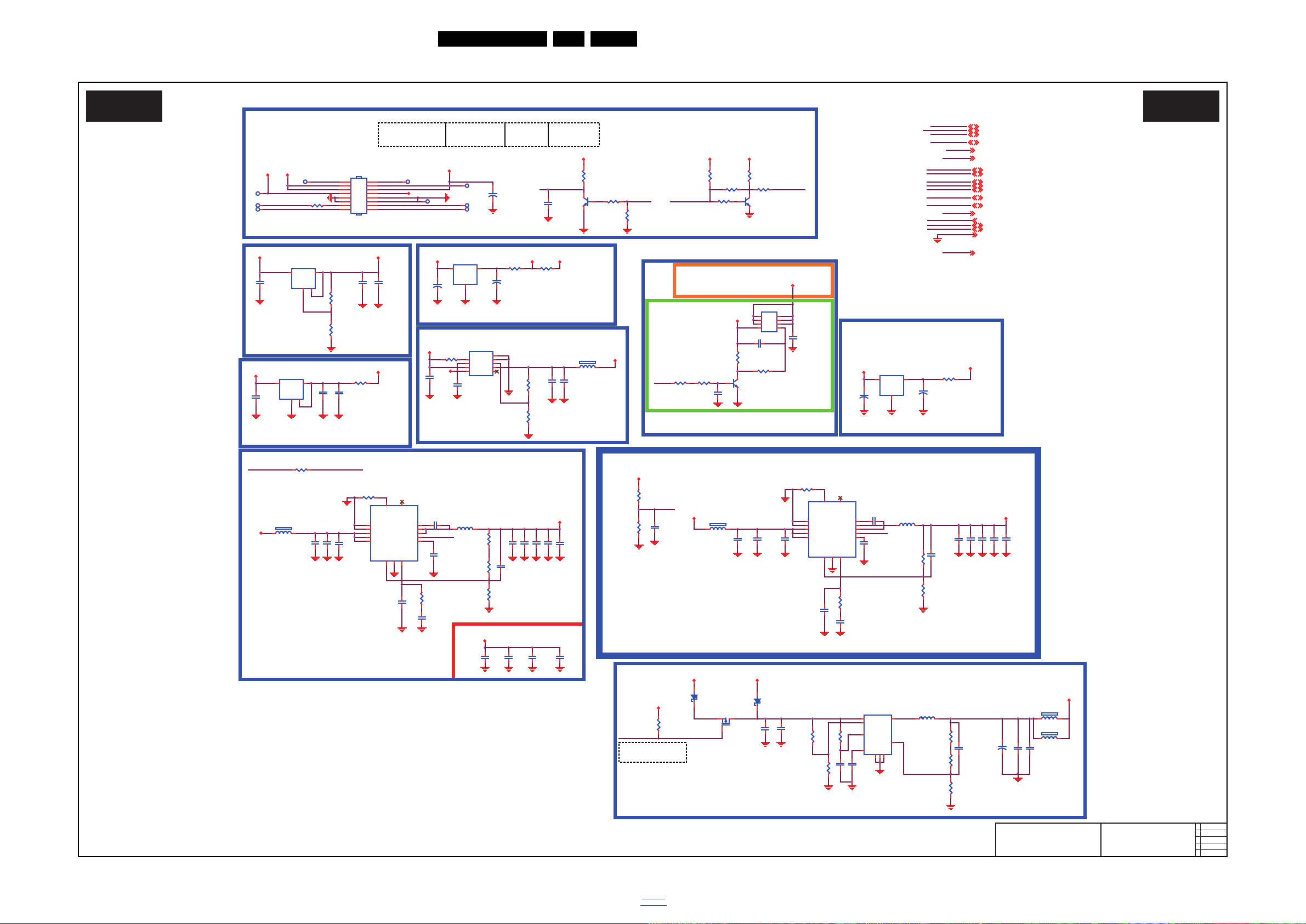
10.3 B 715G7049 SSB
19950_506.eps
System Power 1
B01 B01
2015-04-14
715G7049
System Power 1
TUNER VCC From +5V_SW
U705
uP0126BJT3-33
VI3VO
2
GND14
4
C749
10uF 10V
+3V3_TUNER
+5V_SW
FB706
120R
1 2
DVDD3V3+5V_SW
+
C774
100UF 16V
R4022
NC/0R 05 1/ 16W
C771
10uF 16V
+5V_STB
+5V_STB
R729
10R 1/10W 5%
R4277
0R05 1/4W
TP710
OPWRSB
R4066
0R051/8W
+
C758
100UF 16V
CN700
CONN
2
4
6
8
10
12
14
16
1
3
5
7
9
11
13
15
+
C754
100UF 16V
+5V_STB
U706
AZ1084CS2-3.3TR G1
VIN3VOUT
2
GND
1
3V3SB From +5V_STB
R719
330R 1%
U710 AT1527F11U
VCC
1
REF
2
GND
3
FB
4
EN
5
PGND
6
LX
7
VIN
8
Thermal Pad
9
U708
RT7299BHGQW
RT/SYNC
1
GND
2
GND
3
PVIN
4
PVIN
5
VIN
6
FB7COMP
8
SS/TR
9
EN
10
LX
11
LX
12
BOOT
13
PGOOD
14
E-Pad
15
OPWRSB_PWR
C700
NC/10uF 6.3V
R727
47K 1/16W 5%
R715
20K 1/16W 5%
R701
4K7 1/16W 5%
LDO_PWR From DVDD3V3
R4298 0R05 1/16W
OPWRSB_PWR
C711 22UF 20% 6.3V
DDR_PW R_EN
C727
10uF 16V
C702
22UF 20% 6.3V
L702
2.2uH
D703
SX34
12
FB705
120R
1 2
TP703
Q706
AO3401A
D704
SX34
12
C726
100NF 16V
+5V_SW+5V_STB
C786
10uF 10V
TP701
DDRV
C730
150PF 50V
R4288
0R05 1/4W
C703
100NF 16V
R4289
0R051/8W
C717
100NF 16V
+
C775
100UF 16V
FB704
120R
1 2
C787
10uF 10V
AVDD1V0
Q700
MMBT3904
C713 10NF 50V
R707
3Kohm 1/16W +/-1%
TP705
R728
22K 1/16W 5%
3V3SB
TP700
INVERTER_ON_OFF:
Normal: High
Stand_By: Low
R412
NC 10K 1/16W 5%
DVDD3V3DVDD3V3
ANALOG_DIMMING
R419
NC 4K7 1/16W 5%
R420
NC 4.7K1/ 16W
Q410
NC MMBT3904
BRIGHT_ADJ:
Normal:Max:+3V3, Min:0V
Stand_By:0V
TP702
DC POWER INPUT_12V Only
Stand By:8.5V
LDO_PWR
OPWRSB:
Normal: Low
Stand_by: High
AVDD3V3
+12V_AU
R702
82 KOHM +-5% 1/16W
R718
750R 1%
C734
10uF 16V
TP704
C729
1UF 10V
TP706
+12V
C722
NC 10uF 16V
C725
NC 100NF 16V
C773
10uF 10V
VCCK
C724
NC 100NF 16V
C779
10uF 10V
C742
100N 16V
C744
NC 470PF 50V
C732 10uF 16V
PWR_EN
C728
10uF 10V
C743
100NF 25V
L701 1. 5UH
C721 100NF 16V
C745
8.2NF 50V
R713
0R05 1/16W
C737
10uF 16V
3V3SB
R712
16K 1%
C716
100N 16V
C644 10uF 16V
OPWRSB_PWR
FB710
120R
12
L705
4.7uH 32mOHM
C718
100NF 16V
C645 10uF 16V
R739
100K 1%
C723
NC/1U F 10% 16V
R716
24K 1%
C767
10uF 16V
C712
10uF 16V
R737
13K OHM +-1% 1/16W
R720
100K 1/16W 5%
C769
10uF 16V
U707 AZ1117H-ADJ-E1
VI3VO
2
GND14
4
C709
180PF 50V
C731 10uF 16V
C733
NC 10uF 16V
FB712
120R
1 2
C768
10uF 16V
C720
0805 22uF
+5V_STB+12V
+12V
VCCK
AVDD3V3
R7110 4.7K1/16W
R4023
0R05 1/16W
VCCK
C643
10uF 10V
U701
AZ1084CS2-3.3TR G1
VIN3VOUT
2
GND
1
+5V_STB
R730
2.4K 1% 1/16W
R731
300R 1/16W 1%
+12V_AU 4,14
+12V_AU
R721
4.3K 0.5% 1/16W
2D/3D_SELECT
2D/3D_SELECT 14
+12V to +5V_STB by PSU 12V.
INVERTER_ON_OFF
+
C701 100UF 16V
DDR_PWR_EN 14
DDR_PW R_EN
C788
100NF 16V
C770 10NF 50V
+5V_SW On control by VCCK.
DRAM Power
2D/3D_SELECT:
3D Mode: High
2D Mode: Low
+12V
C748
NC/470PF 50V
TP711
C765 100NF 16V
R703
5.1K 1%
+
C706
100UF 16V
R709
1.6KOHM +- 1% 1/10W
DDR_PW R_EN :
Fast Boot Enable : Low
Fast Boot Disable : High
R417
NC 100R 1/ 10W 5%
BOOST_PWM
BOOST_PWM
BRIGHT_ADJ
R717
100K 1/16W 5%
R708
10K 1/16W 5%
U711
G9661
POK
1
VEN
2
VIN
3
VPP4NC
5
VO
6
ADJ
7
GND
8
E-Pad
9
ANALOG POWER AVDD1V05
AVDD1V05 Fr om AVDD3V3
+5V_EN
PWR_EN
R724
100K 1/16W 5%
+12V
STB_PW R
U702
RT7299BHGQW
RT/SYNC
1
GND
2
GND
3
PVIN
4
PVIN
5
VIN
6
FB7COMP
8
SS/TR
9
EN
10
LX
11
LX
12
BOOT
13
PGOOD
14
E-Pad
15
C714 180PF 50V
DVDD3V3
+5V_EN
DVDD3V3 From +5V_SW
+12V_AU
ANALOG_DIMMING 14
ANALOG_DIMMING
R741
10K 1/10W 5%
+5V_STB
+5V_SW
2D/3D_SELECT
C715
8.2NF 50V
R706
22KOHM 1/10W
Q701
BC847C
R704
33K 1/10W 5%
C763
10UF 10V
R705
2K7 1/16W 5%
C735
100NF 16V
C764
1UF 10% 16V
+5V_SW
Q702
AON4421
D
1
D
2
D
3
G4S
5
D
6
D
7
D
8
+5V_USB
+12V
+5V_USB6
DVDD3V3
+3V3_TUNER
OPWRSB
BRIGHT_ADJ
+5V_STB TO +5V_SW BY VCCK
GND 4,5,6,7,8,9,10,11,12,13,14,15,16,17
OPWRSB5
DDRV
INVERTER_ON _OFF
DVDD3V3 5, 6,8,10,11, 14,15,16,17
INVERTER_ON _OFF 10
BRIGHT_ADJ 10
AVDD3V3 6,7,10, 15
+3V3_TUNER 16
3V3SB 5,6,7,10,14,15
VCCK 5,11,14
+12V 4,6,17
AVDD1V0 6,10,15
+5V_SW 4,6,7,10,15
DDRV 11,12,13
AVDD3V3
+5V_SW
VCCK
3V3SB
AVDD1V0
R714
680R 1/16W 5%
R723
33K 1/16W 5%
C736
10uF 10V
10-3-1 System power 1
Circuit Diagrams and PWB Layouts
EN 48QM16.1L LA 10.
2016-Jul-08
back to
div.table
Page 49
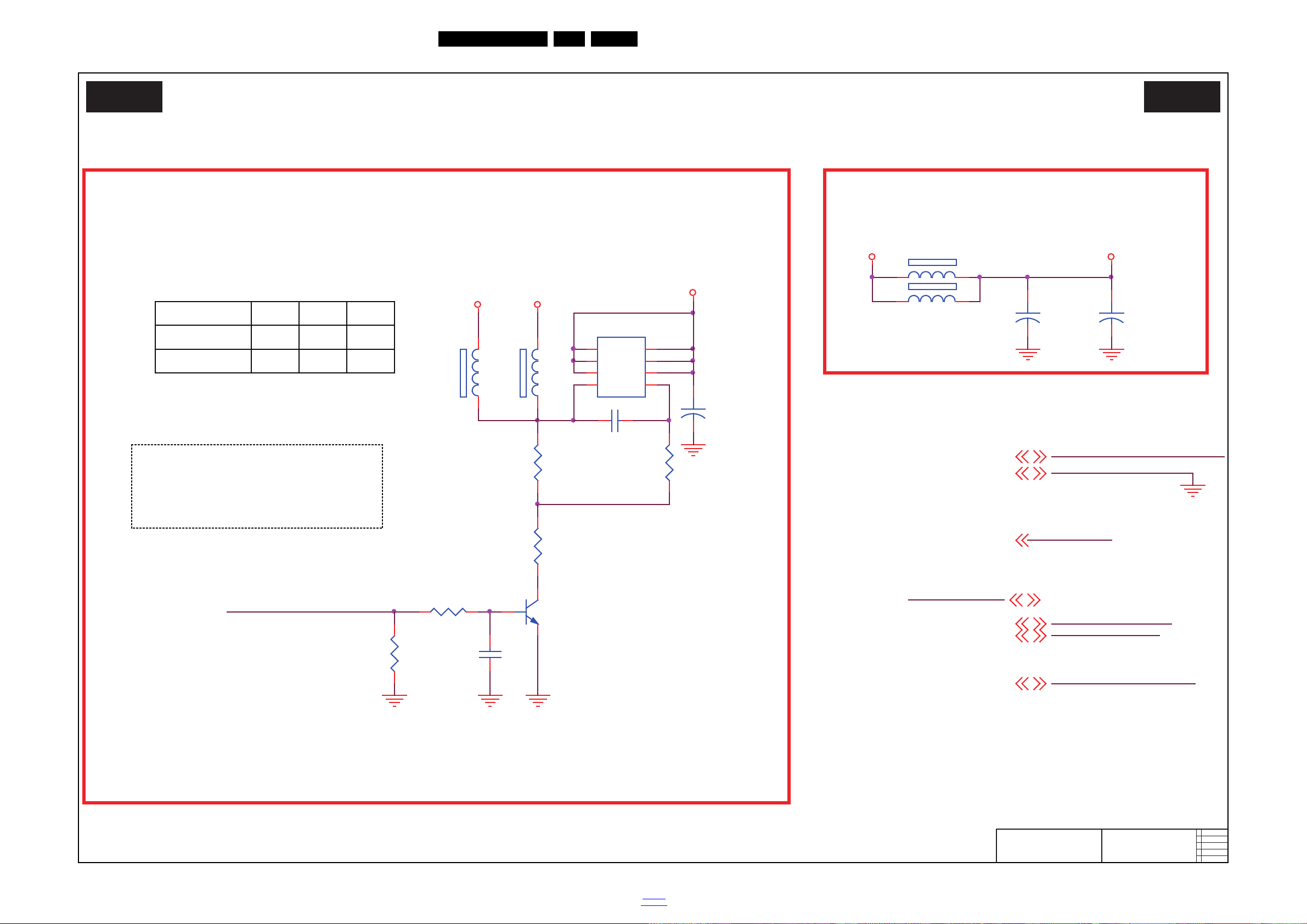
10-3-2 System Power 2
19950_507.eps
System Power 2
B02 B02
2015-04-14
715G7049
System Power 2
+
C762
220uF 16V
R753
6K8 1/10W 5%
FB751
NC 120R
1 2
FB754
120R
12
R750
10K 1/16W 5%
R759
10K 1/16W 5%
R752
10K 1/10W 5%
FB755
120R
1 2
+12V_AU 3,14
+12V_AU
Q750 AON4421
D
1
D
2
D
3
G
4
S
5
D
6
D
7
D
8
C750
1UF 10% 16V
C751
NC/4.7UF 10V
Q751
BC847C
FB750
120R
1 2
R751
5.1KOH M +-5% 1/10W
PANEL_VCC
+12V+5V_SW
PVDD
+12V_AU
PANEL_VCC_ON/OFF10,17
GND3,5,6,7,8,9,10,11,12,13,14,15,16,17
DVDD3V33,5,6,8,10,11,14,15,16,17
+
C766
220uF 16V
PVDD8
+5V_SW3,6,7,10,15
+12V3,6,17
+
C752
220UF 16V
Panel VCC=12V or 5V
PANEL_VCC ON/OFF:(OPCTRL9)
Normal:High
Stand_By:Low
PANEL_VCC_ON/OFF
GND
PANEL_VCC_ON/OFF
Audio VCC= +12V
Yes
0R
5.1K
R751
NC
NC
Yes
+12V
FB751FB750
PANEL VCC
+5V
DVDD3V3
PVDD
+5V_SW
+12V
Circuit Diagrams and PWB Layouts
EN 49QM16.1L LA 10.
2016-Jul-08
back to
div.table
Page 50
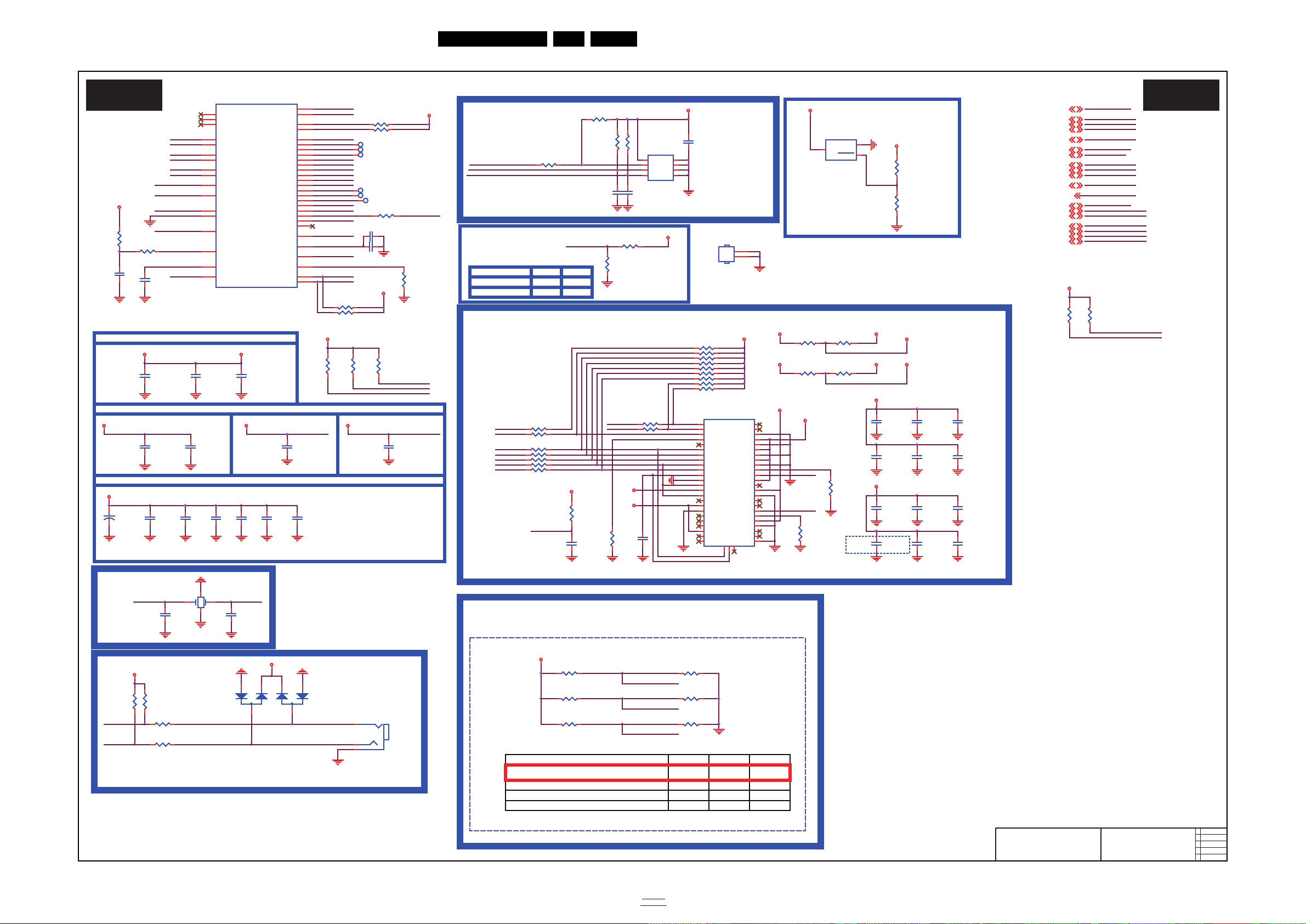
10-3-3 Peripheral
19950_508.eps
Peripheral
B03 B03
2015-04-14
715G7049
Peripheral
TP818
PDD0
C4039
1UF 6. 3V
TP816
PDD6
PAALE
POCE0#
PACLE
PDD5
R4034 4K7 1/16W 5%
PDD4
R4033 4K7 1/16W 5%
POWE#
PDD1
U0TX
DVDD3V3
PDD7
POOE#
RXD_RF4CE
PDD3
PARB#
EMMC_CLK
PDD2
U0RX
TP819
POCE1#
TXD_RF4CE
TP820
C4033
100NF 16V
PACLE
PAALE
EMMC_RST#
TP817
R4287
NC/ 0R 05 1/ 10W
R4060 NC 10K 1/ 16W 5%
OPWRSB
C601
100NF 16V
EMMC VCC/VCCQ Power
C4014
10NF 50V
ORESET#
EMMC
3V3SB
RC6
C4037
100NF 16V
R4035
4K7 1/16W 5%
R4036
4K7 1/16W 5%
VCC3IO_EMMC
FSRC_WR
R4005
4K7 1/16W 5%
Cobra RAV0.3_20120502
E-Fuse
CN412
PHONE J AC K
1
2
3
C4023
100NF 16V
R4003
0R05 1/16W
R4002
2K7 1/16W 5%
3V3SB
OSDA1
MT5593UPIJ
U401-7
OSDA0
AT37
OSCL0
AT38
OSDA1
AN38
OSCL1
AN37
XTALO
E38
XTALI
E37
AVDD33_REG_STB
AA36
AVDD33_RGB_STB
U38
AVSS33_RGB
M25
AVDD33_PLL_STB
Y36
AVDD10_LDO
V36
U0TX
AE36
U0RX
AE37
U1RX
AM37
U1TX
AM38
POWE__B
AG38
POOE__B
AH37
POCE1__B
AF36
POCE0__B
AF38
PDD7
AJ33
PDD6
AJ34
PDD5
AJ35
PDD4
AH34
PDD3
AH32
PDD2
AF32
PDD1
AF33
PDD0
AJ37
PARB__B
AH36
PACLE
AG37
PAALE
AE34
OPWRSB
AB38
ORESETB
M34
OIRI
Y35
FSRC_WR
G20
STB_SCL
AC37
STB_SDA
AC38
EMMC_CLK
AL37
AVDD10_ELDO
V37
POR_OPT
U34
VCC3I O_EMMC
AJ38
CPC0
U33
CPC1
V33
CPC2
V34
EMMC_RSTB
AK36
DS
AJ32
C4038
100NF 16V
R4056 NC 10K 1/ 16W 5%
ORESET#
SYS_EEPROM_WP
GND
OPWRSB
R4297
0R05 1/10W
PDD5
C4035
10UF 6.3V 20%
R4054 NC 10K 1/ 16W 5%
+5V_STB3
+5V_STB
C4034
100NF 16V
R4061 NC 10K 1/ 16W 5%
VCC3I O_EMMC
R4058 NC 10K 1/16W 5%
RC66
RC6
C4043
10UF 6.3V 20%
R4057 NC 10K 1/ 16W 5%
C4045
NC/10UF 6.3V 20%
C4016
10UF 6. 3V 20%
3V3SB
LDO_PWR
R4059 NC 10K 1/ 16W 5%
C4017
1UF 6. 3V
C4044
10UF 6. 3V 20%
R4028
4K7 1/16W 5%
OSCL1
EMMC_RST#
C4036
10UF 6. 3V 20%
R4055 NC 10K 1/ 16W 5%
R4053 NC 10K 1/16W 5%
VCC_EMMC
VCC3IO_EMMC
VCC3I O_EMMC
VCC_EMMC
VCC3I O_EMMC
VCC_EMMCDVDD3V3
VCC3I O_EMMC
DVDD3V3
VCC3IO_EMMC
C4019 NC 10UF 10V
R4062
NC 10K 1/16W 5%
R4280
0R05 1/10W
TP450
R4291
NC/ 0R 05 1/ 10W
R4067
0R05 1/16W
R4068
0R05 1/16W
POWE
0
1
LED_PWM2
0
0
1
ICE mode + 24M + serial boot(with GPIO)
ICE moce + 24M + ROM to eMMC boot from
eMMC pins (share pins w/s NAND)
LED_PWM0
0
ICE moce + 24M + ROM to 60bit ECC Nand boot
ICE mode + 24M + serial boot
0
0
1
0
0
LED_PWM1
STRAPPING
1
3.3V IO Power
PDD4
I2C Address "A0"
VCCK
LED_PWM06,14
LED_PWM16,14
LED_PWM1
LED_PWM0SYS_EEPROM_WP
LDO_PWR
R671
NC 4K7 1/ 16W 5%
R672
NC 4K7 1/16W 5%
R673
NC 4K7 1/ 16W 5%
DVDD3V3
POOE#
POCE1#
PARB# VCC_EMMC
R675
4K7 1/16W 5%
R674
4K7 1/16W 5%
DVDD3V3
AVDD33_PLL_STB
AVDD33_REG_STB
DVDD3V3
R689
47R +-1% 1/16W
HS401
HEAT SINK
1
2
R4010
2K 1/16W 5%
LED_PWM214
LED_PWM2
R4011
2K 1/16W 5%
R690
47R +-1% 1/16W
R691
47R +-1% 1/16W
AVDD33_REG_STB
AVDD33_RGB_STB
R692
47R +-1% 1/16W
C5010
NC 100pF 50V
PDD7
PDD2
C5011
NC 100pF 50V
D4001
NC/BAV99
3
1
2
C4005
22PF 50V
For code download,debugging,factory alignment and compair mode.
C4027
NC 10UF 6.3V 20%
AVDD33_PLL_STB
R4040
20K 1%
OSDA0
C4011
100NF 16V
Core Power
OSDA0
OSCL0
C4022
1UF 10% 16V
U410
NC/AZ809ANSTR-E1
GND
1
RESET
2
Vcc
3
VCC_EMMC
R4029
100R 1/16W 5%
C4008
100NF 16V
AVSS33_RGB_STB
AVDD33_RGB_STB
EMMC_RST#
D4000
NC/BAV99
3
1
2
C4004
22PF 50V
X40 00
24MHz
1
2 4
3
C4012
100NF 16V
R4009
NC 4K7 1/ 16W 5%
U409
NC C AT24C128WI-GT3
A0
1
A1
2
A2
3
VSS4SDA
5
SCL
6
WP
7
VCC
8
AVDD10_LDO
C4024
4.7UF 6. 3V
EMMC_CLK#
AVDD10_ELDO
R4042
47R +-1% 1/16W
C4031
4.7UF 6. 3V
C4013
10UF 10V
C4006
4.7UF 6. 3V
Reset IC
VCC3IO_EMMC
R693 47R +-1% 1/16W
OXTALO
+
C4015
100UF 16V
R4007
NC 0R 05 1/ 16W
R694 47R +-1% 1/16WC4010
100NF 16V
R4031
4K7 1/16W 5%
R695 47R +-1% 1/16W
R696 47R +-1% 1/16W
R697 47R +-1% 1/16W
R4032
4K7 1/16W 5%
R4021
27K 1/16W 1%
R4030
100R 1/16W 5%
C4009
NC 100N F 16V
VCCK
DVDD3V3
OXTALO
OXTALI
3V3SB
EMMC_CLK#
3V3SB3V3SB
DVDD3V3
3V3SB
3V3SB
3V3SB
3V3SB
SYS_EEPROM_WP14
OPWRSB3
PDD3
OSCL08
OSDA08
GND3,4,6,7,8,9,10,11,12,13,14,15,16,17
OSCL0
3V3SB3,6,7,10,14,15
OSDA0
DVDD3V33,6,8,10,11,14,15,16,17
AVDD3V33,6,7,10,15
VCCK3,11,14
U4052
THGBMBG6D1KBAIL
DAT0
A3
DAT1
A4
DAT2
A5
VSS
A6
NC
A7
DAT3
B2
DAT4
B3
DAT5
B4
DAT6
B5
DAT7
B6
VDDI
C2
Vssq
C4
Vccq
C6
NC
C5
Vcc
E6
Vss
E7
NC
E8
NC
E9
Vcc
F5
NC
F10
Vss
G5
NC
G10
NC
G3
DS
H5
Vss
H10
VSS
J5
Vcc
J10
RSTN
K5
NC
K6
NC
K7
Vss
K8
Vcc
K9
NC
K10
Vccq
M4
CMD
M5
CLK
M6
Vssq
N2
Vccq
N4
Vssq
N5
Vccq
P3
Vssq
P4
Vccq
P5
Vssq
P6
NC
P7
NC
P10
A1 index
D4
NC
E5
NC
E10
NCB1NCC1NC
N1
OXTALI
PDD6
24MHz CR YSTAL
Pin7 WP
OSCL0
HI = > Disable write
LO = > Enable Write
SYSTEM EEPROM
VCC3IO_AB
VCC3IO_AB
VCC3IO_AB3,6,8,10,11,14,15,16,17
OSDA16
OSCL16
OSCL1
OSDA1
POWE
OSDA1
OSCL1
AVDD3V3
C4311
NC 100NF 16V
C4312
100NF 16V
C4313
100NF 16V
C4314
100NF 16V
C4315
22UF 20% 6.3V
R4001
0R05 1/16W
R4019
NC 4K7 1/ 16W 5%
U0TX
POR
Internal POR
R4001
0R
NC
External ResetNC4.7K
R4019
U0RX
Analog Power
POR_OPT
POWE#
POR_OPT
3V3SB
R4017
NC 4K7 1/ 16W 5%
R4016
10K 1/16W 5%
R4020
NC 4K7 1/ 16W 5%
R4013
10K 1/16W 5%
R4014
10K 1/16W 5%
LED_PWM0
Cobra RAV0.3_20120502
3V3SB
Cobra RAV0.2_20120411
LED_PWM2
STRAPPING
STB_SCL
STB_SDA
R4018
NC 4K7 1/ 16W 5%
STB_SDA10
STB_SCL10
STB_SCL
STB_SDA
LED_PWM1
Circuit Diagrams and PWB Layouts
EN 50QM16.1L LA 10.
2016-Jul-08
back to
div.table
Page 51
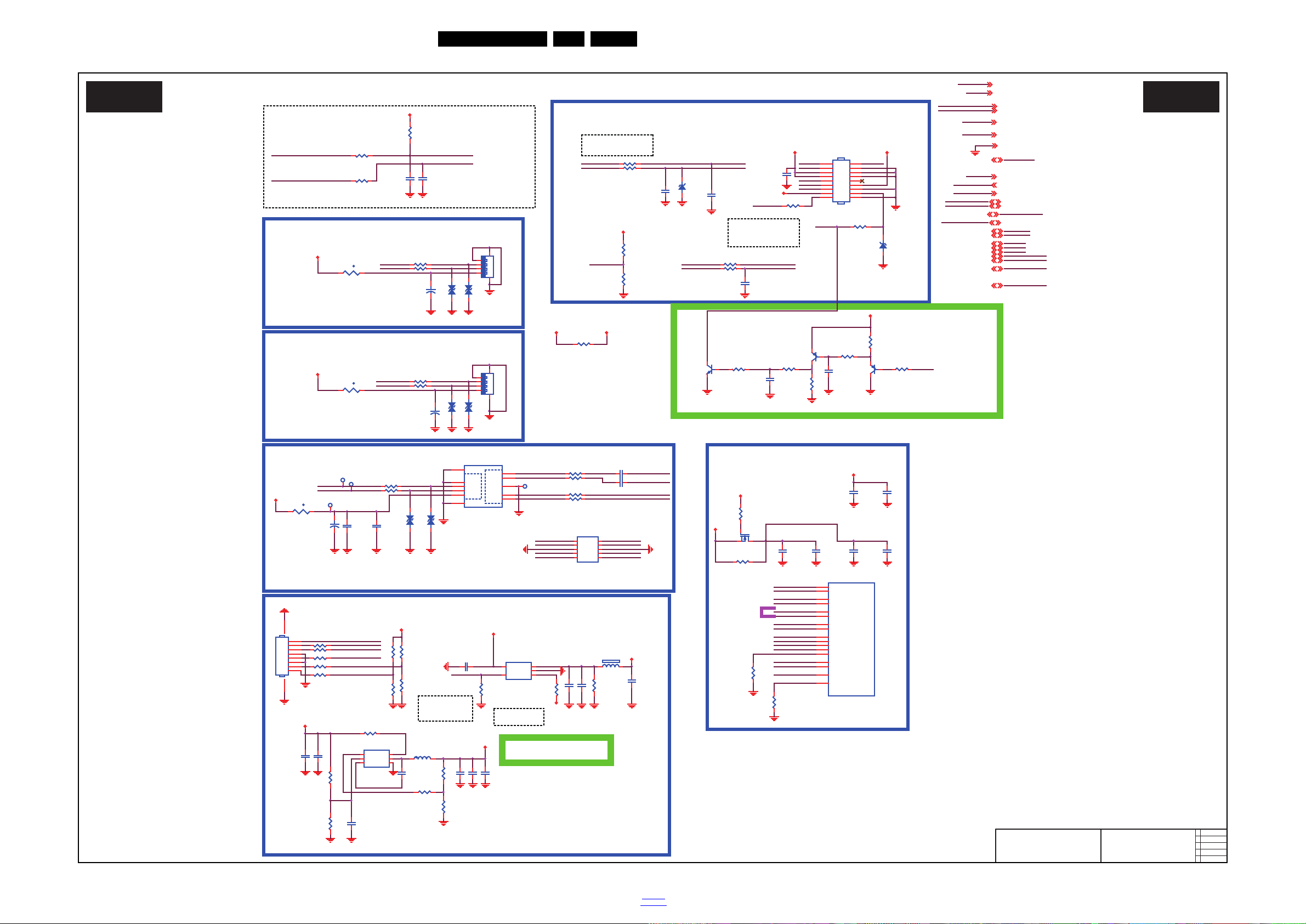
10-3-4 Connector/USB/WIFI
19950_509.eps
Connector/USB/WIFI
B04 B04
2015-04-14
715G7049
Connector/USB/WIFI
KEY_PAD0 14
LED_PWM0 5, 14
LED_PWM0
GND 3,4,5,7,8,9,10,11,12,13,14, 15,16,17
3V3SB 3,5,7,10,14,15
+5V_USB
DVDD3V33,5,8,10, 11,14,15,16, 17
AVDD3V33,7,10,15
+5V_SW 3,4,7,10,15
+12V 3,4,17
Key1KEY_PAD0
TO KEY PAD BOARD
WoBLE-IRQ14
WoBLE-IRQ
RC6#
LED_PWM1
SSUSB_TXN_R
W/S/W
U1101
NC/AOZ8804DI
CH1
1
CH2
2
VN
3
CH3
4
CH45NC
6
NC
7
VN
8
NC
9
NC
10
7.5/7.5/7.5
EQUAL LENGTH and
DIFFERENTIAL
IMPEDANCE 90ohm
USB PORT 1 (SIDE)
C608
NC 10UF 6. 3V 20%
USB_DP_P1
USB_DM_P1
C4242 10uF 16V
C4241 10uF 16V
Q4003
AO3414
WoBLE-IRQ
R4135 0R05 1/16W
R4136 0R05 1/16W
R4137 0R05 1/16W
R4202
0R051/8W
R4138 0R05 1/16W
MT 55 9 3UPIJ
U401-9
USB_DP_P0
A16
USB_DM_P0
B16
USB_DP_P1
A17
USB_DM_P1
B17
USB_DP_P2
C31
USB_DM_P2
D31
USB_DP_P3
AA37
USB_DM_P3
AA38
AVDD33_USB
N28
AVDD33_SSUSB
A33
SSUSB_TXP
B34
SSUSB_TXN
A34
SSUSB_RXP
B32
SSUSB_RXN
A32
AVDD10_SSUSB
A31
SSUSB_VRT
A35
USB_VRT_P0
B15
SSUSB_TXP_R
SSUSB_TXN_R
SSUSB_RXP_R
SSUSB_RXN_R
C1116
100NF 16V
C1117
100NF 16V
Wi-Fi_VCC14
USB_DM_P3
USB_DM_P1
Wi-Fi_VCC
SSUSB_TXN
SSUSB_TXP
USB_DP_P3
USB_DP_P1
USB_DM_P0
USB_DP_P0
SSUSB_RXN
SSUSB_RXP
TP337
TP353
USB_DP_P2
USB_DM_P2
TP285
USB 3.0
R732
5.1K 1%
R733
5.1K 1%
SSUSB_VRT
R4254
10K 1/16W 5%
LED_R:
Enable(Stand_By) : High
Disable: Low
+5V_USB
+5V_SW
USB_VRT_P0
+5V_USB
C4113
NC/100N 50V
3V3SB
SSUSB_TXP
R4255
NC 0R05 1/ 16W
SSUSB_TXN
TO IR/KEY BOARD
SSUSB_TXP_R
SSUSB_RXP
SSUSB_RXN
AVDD33_USB
AVDD33_SSUSB
C4129
1UF 6.3V
AVDD1V0
AVDD3V3
C4131
100NF 16V
AVDD10_SSUSB
C4130
1UF 6.3V
AVDD10_SSUSB
LS_SDA
3V3SB
3D_L/R_IN10,14
3D_L/R_IN
LED_R
C4244 100NF 16V
CN401
CONN
2
4
6
8
10
12
14
16
18
1
3
5
7
9
11
13
15
17
C4117
NC/100N 50V
LOGO
SSUSB_TXN_R
Key1 17
Key1
U4251
MP1470GJ
-Z
GND
1
SW
2
IN3FB
4
EN
5
BST
6
+12V
C4246
10uF 16V
C4245
10uF 16V
L4201
4.7UH
SSUSB_RXP_R
ZD4101 NC/M M3Z5V6B
DVDD3V3
LED_PWM15,14
LED_PWM1
W/S/W
Gaming :
2D Dual View Mode :
High
Normal 3D Mode : Low
Key1
7.5/7.5/7.5
Wi-Fi Power Control
Wi-Fi_OCP :
Disable :
Low
R/A
USB_DP_P2
USB_DM_P2
WoWLAN_IRQ
WIFI_PWR_EN14
WIFI_OCP10
WoWLAN_IRQ14
WIFI_OCP
WIFI _PWR_EN
ZD1101
NC/VPORT0603100KV05
12
SSUSB_RXN_R
Reserve USB 3.0 (SIDE)
t
TH4102
PTCR
1 2
LS_SCL
C4116 N C / 10N 50V
ZD1102
NC/VPORT0603100KV05
12
KEY_PAD0
C4247
1UF 10% 16V
R4285 0R05 1/16W
Wi-Fi_VCC
R4286
10K 1/16W 5%
SSUSB_RXP_R
W/S/W
R4284
0R051/8W
7.5/7.5/7.5
EQUAL LENGTH and
DIFFERENTIAL
IMPEDANCE 90ohm
USB PORT 2 (DOW N)
USB_DP_P3
USB_DM_P3
R4256 0R05 1/16W
R4064
3K3 1/16W 5%
Wi-Fi_RESET
R4257
10K 1/16W 5%
LS_SDA
R4258
NC 10K 1/16W 5%
USB2.0
USB3.0
CN4102
USB CONN 9P
HAND1
10
HAND2
11
VCC
1
D+
3
GND
4
D-
2
RXN
5
RXP
6
GND
7
TXN
8
TXP
9
R4290
NC 10K 1/16W 5%
SSUSB_RXN_R
C4243
100NF 16V
ZD1103
NC/VPORT 0603100KV05
12
ZD1104
NC/VPORT 0603100KV05
12
ZD4102
NC/MM3Z 3V6B
1 2
R7106 1K
3D_L/R_IN
WIFI_PWR_EN WIFI_OCP
USB_DM_P0
USB_DP_P0
U4250
APL3511ABI-TRG
VOUT
1
GND
2
OCB3EN
4
VIN
5
C4251
1UF 10% 16V
R4252
4K7 1/16W 5%
FB4250
120R
1 2
R4251
4K7 1/16W 5%
R4265 2R2 1/16W 5%
R4264 2R2 1/16W 5%
C4253100NF 16V
C425010U F 10V
R4250
10K 1/16W 5%
C4252
10UF 10V
WIFI_PWR
3V3SB
Add for 3D interference
suppression
Wi-Fi_VCC
Wi-Fi_VCC
AVDD1V0 3,10, 15
WoWLAN_IRQ
AVDD1V0
R4278
10K 1/16W 5%
LOGO
OSDA1 5
OSCL1 5
OSDA1
OSCL1
R4063
40.2K 1/16W 1%
Wi-Fi_RESET10
Wi-Fi_RESET
Q606
NC BC857BW
1
23
Q607
NC BC857BW
1
23
Q608
NC BC847C
R4269
13K 1%
RC65
RC6
R682
NC 1K
RC6#
R4065
75K 1/16W 1%
R683
NC 2.7K 1%
ZD1105
NC/VPOR T0603100KV05
12
ZD1106
NC/VPOR T0603100KV05
12
AVDD33_USB
C4127
1UF 6.3V
C4126
NC 100NF 16V
3V3SB
+5V_USB
AVDD3V3
AVDD33_SSUSB
R684
NC 3.3K 1/16W
C4128
100NF 16V
Wi-Fi_PWR_EN :
Enable : High
Disable : Low
C784
NC 1uF 10V
WIFI_PWR: (Stand By Mode)
PSU 12V Stand By-->8.5V
1234
CN4101
USB CONN
1
2
3
4
65
C785
NC 1uF 10V
+5V_SW
WIFI_PWR
+
C4108
100UF 16V
R4105 2R2 1/16W 5%
t
TH4100 PTCR
1 2
TP118
R4104 2R2 1/16W 5%
R685
NC 10K 1/16W 5%
t
TH4101 PTCR
1 2
R4111 2R2 1/16W 5%
C4106
0.1uF 50V
R686
NC 100OHM
R4106
100R 1/10W 1%
R4112 2R2 1/16W 5%
R687
NC 100K 1/16W 5%
R4102
100R 1/10W 1%
R6762R2 1/ 16W 5%
R6772R2 1/ 16W 5%
R4273 0R05 1/16W
C4107
0.1uF 50V
SSUSB_TXP_R
+5V_SW
R4100
6.8K +-1% 1/16W
3D_L/R10,14
Gaming14
3D_L/R
Gaming
1234
CN4100
USB CONN
1
2
3
4
65
R4121 100OHM
+12V
+
C4111
100UF 16V
3V3SB
Gaming
OSDA1
+5V_USB
R7107
NC/10K
R7108
NC/10K
R7105
100OHM
+5V_SW
R4122 100OHM
RC6
LS_SCL
C1115
NC 10UF 6. 3V 20%
+5V_USB
LED_PWM0 LED_R
OSCL1
CN4250
CONN
1
2
3
4
5
6
7
8
910
R4117 100OH M
Gaming
RC6#
R4114 100OH M
3D-IR-OUT
+
C1080
100UF 16V
DVDD3V3
C4115
NC/10uF 6.3V
DVDD3V3
Circuit Diagrams and PWB Layouts
EN 51QM16.1L LA 10.
2016-Jul-08
back to
div.table
Page 52
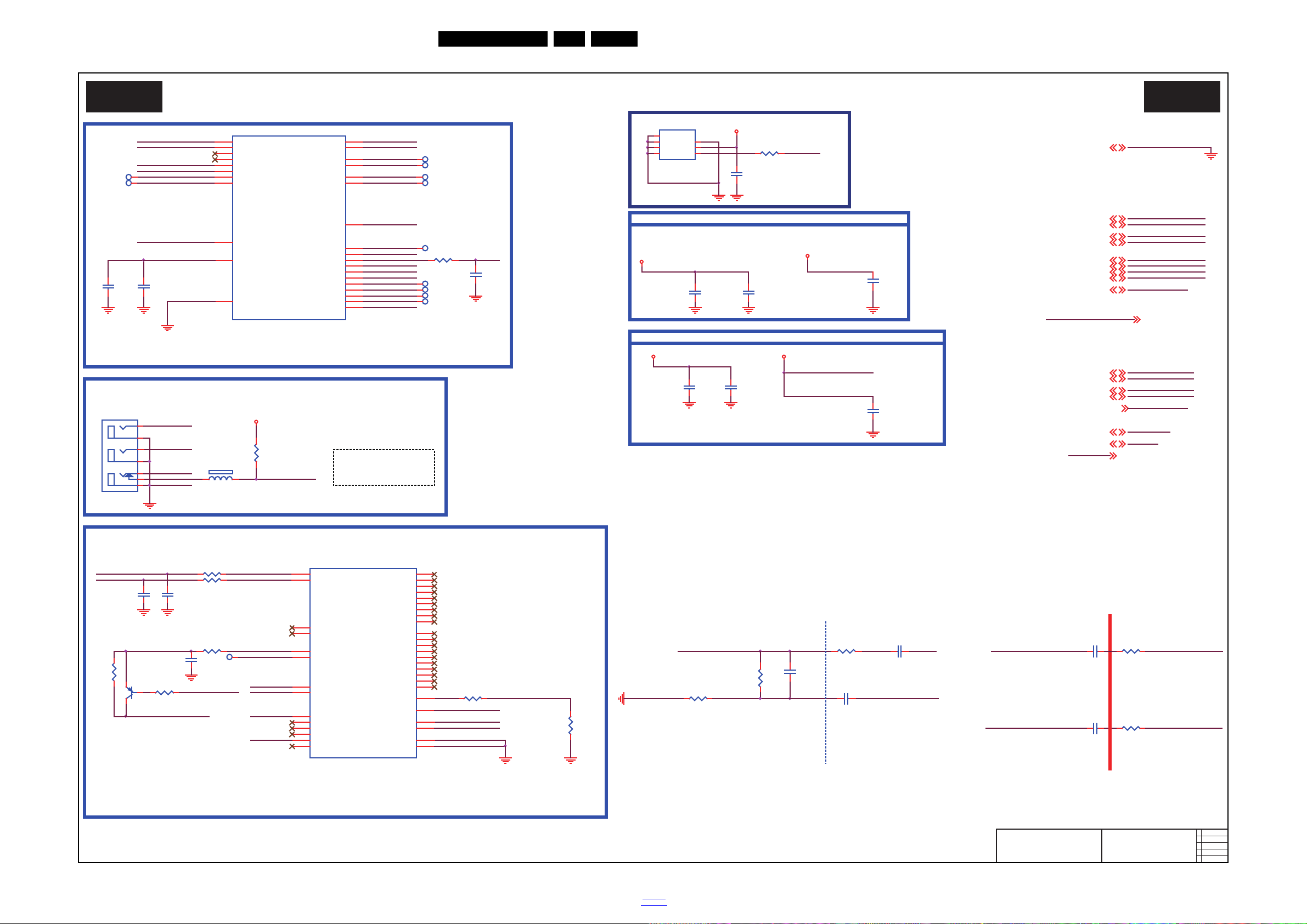
10-3-5 Audio /Video IO/SPDIF
19950_510.eps
Audio /Video IO/SPDIF
B05 B05
2015-04-14
715G7049
Audio /Video IO/SPDIF
R1071
NC 75 OH M +-5% 1/ 16W
CN6003
JACK
VIN
1
VCC
2
GND
3
TH1
4
TH2
5
TH3
6
TH4
7
DVI_R_IN
GND
DVI_L_IN
AOSDATA0_D
AOMCLK_D
AOBCLK_D
AR0O
AL0O
AOLRCK_D
AVSS33_XTAL_STB
C603
100NF 16V
AVDD3V3
C1040
1UF 10% 16V
AVDD33_XTAL_STB
3V3SB
AVDD33_AADC
CVBS_DETECTN14
CVBS0PCV1_AV_IN
AVDD33_XTAL_STB
C602
100NF 16V
R1088
30Kohm 1/16W +/ -5%
C1039
1UF 10% 16V
R1087
30Kohm 1/16W +/ -5%
AVDD3V3
CVBS_DETECTN
3V3SB
DVI_R_IN9
R1072 10R 1/16W 1%
DVI_L_IN9
GND3,4,5,6,8,9,10,11,12,13,14,15,16,17
AL0O8
AR0O8
AOLRCK_D8
AOBCLK_D8
AOMCLK_D8
AOSDATA0_D8
TU_FAT_IN2+16
TU_FAT_IN2-16
OSCL216
OSDA216
IF_AGC16
AVDD3V33,6,10,15
ARC15
TUN ER _BY PASS_OUT
AVDD33_DEMOD_STB
R7121
10K 1/16W 5%
CV1_AV1_GND
SPDIF_OUT
+5V_SW
C613
100NF 16V
R606
33R 1/16W 5%
Analog Power
C612
100NF 16V
C614
10UF 6. 3V 20%
C611
100NF 16V
AVDD3V3
AVDD33_ADAC
CVBS1_L_IN
CVBS1_R_IN
Analog Power
IF_AGC
CV1_L_IN
AIN4_R_IN
DVI_L_IN
TP612TP
DVI_R_IN
CV1_R_IN
TP613TP
AIN4_L_IN
AVDD33_AADC
VMID_AADC
C610
100NF 16V
C606
1uF 10V
CV1_L_IN
CV1_R_IN
MT5593UPIJ
U401-4
AVDD33_AADC
M26
VMID_AADC
D38
AL2_ADAC
E35
AL0_ADAC
C35
AR0_ADAC
D36
AL1_ADAC
E36
AR1_ADAC
D35
AR2_ADAC
C36
ASPDIFI
AR38
ASPDIFO0
AB34
ASPDIFO1
G27
AOBCK
AM31
AOLRCK
AN30
AOMCLK
AP36
AOSDATA4
AN33
AOSDATA3
AM33
AOSDATA2
AL31
AOSDATA1
AM30
AOSDATA0
AN31
AVDD33_ADAC
M27
AIN_R0
B36
AIN_L0
D37
AIN_R1
A37
AIN_L1
C38
AIN_R2
B38
AIN_L2
B35
AIN_R3
A36
AIN_L3
C37
AVSS33_CLN
M24
CVBS_COM
AVSS33_CLN
CVBS1_L_IN
A
B
C
CN600
RCA JACK 7P
2
1
4
3
6
5
7
TU_FAT_IN2+
R603
51OHM 1/16W +/ -5%
TU_FAT_IN2- ADCINN_DEMOD
ADCINP_DEMOD
R604
51OHM 1/16W +/ -5%
C622
47PF 50V
C623
47PF 50V
AVDD3V3
AR0O
TP609 TP
AL0O
TP608 TP
AR2O
TP610 TP
TP611 TP
AL2O
AL1O
AR1O
AVDD33_ADAC
TP451 TP
TP452 TP
ARC
AOMCLK_D
TP614 TP
AOBCLK_D
TP453 TP
AOSDATA4
AOSDATA2
C4317
22PF 50V
AOLRCK_D
AOSDATA0_D
SPDIF_OUT
AU_DIN
AOSDATA3
TP454 TP
AOSDATA1
R1011
100R 1/16W 5%
R7155
100R 1/16W 5%
IF_AGC
C621
47NF 16V
R605 10K 1/ 16W
Video
+5V_SW
+5V_SW 3,4,6,10,15
Audio
CVBS_DETECTN :
Cable connec t ed : High
Cable not c onnec ted : Low
C1009
47NF 16V
C1010
47PF 50V
R1012
75 OHM +-5% 1/16W
R/A TYPE
MT5593UPIJ
U401-5
ADCINP_DEMOD
F38
ADCINN_DEMOD
F37
IF_AGC
B14
RF_AGC
C15
OSCL2
E18
OSDA2
F18
CVBS3P
J38
CVBS2P
K35
CVBS1P
K34
CVBS0P
H38
CVBS_COM
J36
HSYNC
R37
VSYNC
T36
RP
N37
GP
P37
BP
R38
COM
P36
SOG
P38
VGA_SDA
U36
VGA_SCL
T37
COM1
M38
PB1P
M36
PR1P
L38
Y1P
M37
SOY1
N36
COM0
K37
PB0P
K36
PR0P
J37
Y0P
L36
SOY0
L37
VDACX_OUT
K33
AVDD33_VIDEO_STB
M35
AVDD33_DEMOD_STB
G38
AVSS33_XTAL
N25
AVSS33_DEMOD
N24
LOUTP
L26
LOUTN
L27
AVDD33_XTAL_STB
G37
SIF_COM
H37
TP603
RF_AGC
OSDA2
OSCL2
CVBS0P
C607
1uF 10V
ARC
CVBS_COM
CVBS_DETECTN
CV1_AV_IN
FB1001
120R
1 2
C604
10UF 6. 3V 20%
AVDD33_VIDEO_STB
CVBS1_R_IN
OSDA2
OSCL2
Q609
BC857BW
1
23
R698 100K 1/16W 5%
AVDD33_DEMOD_STB
TU_FAT_IN2+
TU_FAT_IN2-
RF_AGC
AVSS33_DEMOD
IF_AGC_ATV
R699
NC 0R 05 1/ 16W
3V3SB 3,5,6,10,14,15
3V3SB
(20mil)
(20mil)
Y
R
CV1 IN (R/A)
10.5mm
W
R688 0R05 1/16W
CV1_AV1_GND
CV1_AV_GND
AVDD33_VIDEO_STB
CV1 IN
(20mil )
Circuit Diagrams and PWB Layouts
EN 52QM16.1L LA 10.
2016-Jul-08
back to
div.table
Page 53
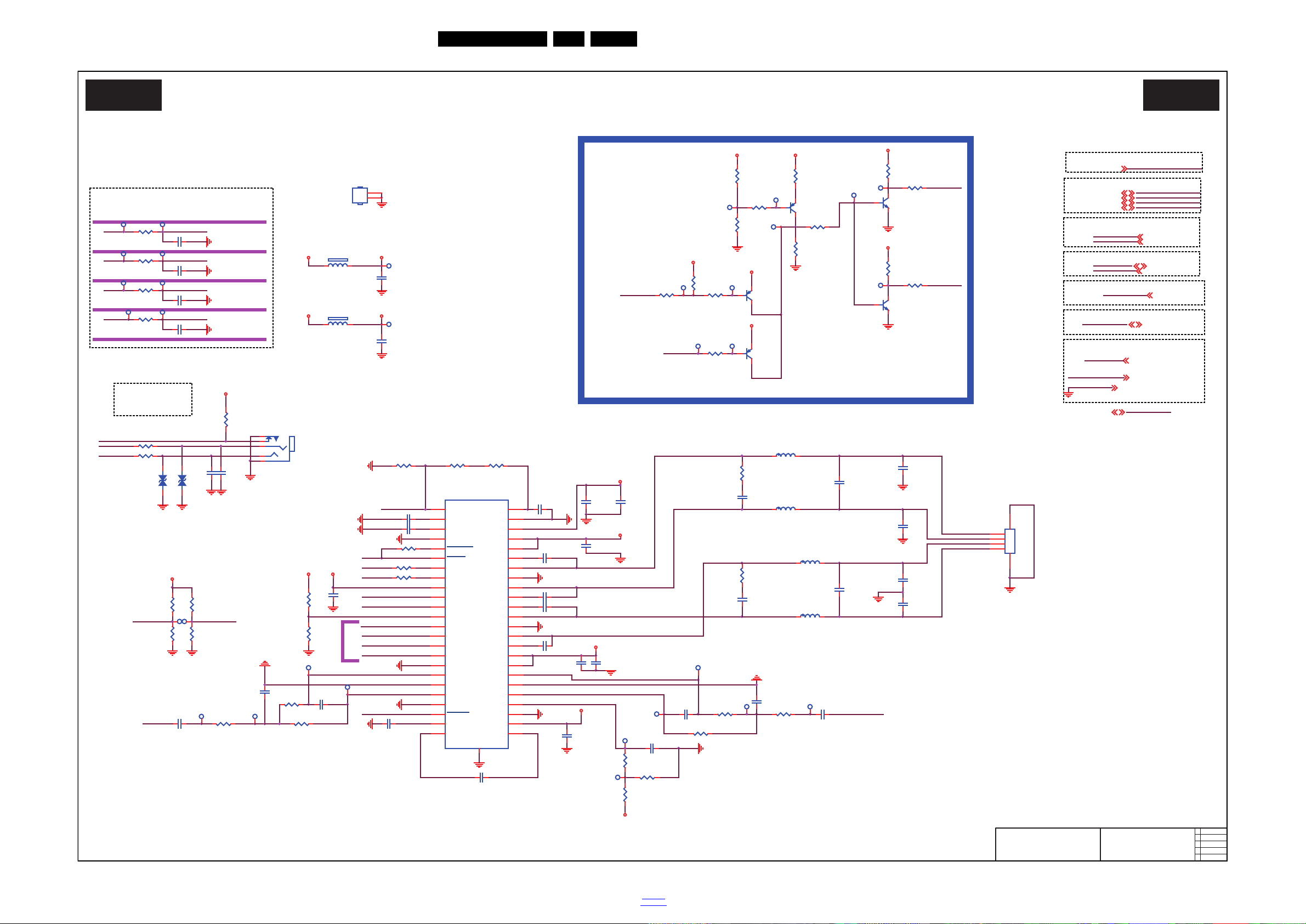
10-3-6 Speaker/Headphone
19950_511.eps
Speaker/Headphone
B06 B06
2015-04-14
715G7049
Speaker/Headphone
LSPK+
R617
0R05 1/16W
R618
0R05 1/16W
Grounding
R680 10R 1/ 16W 1%
Power
Item number from 630
SPK Mute Control
Grounding
LSPK-
Q605
BC857BW
1
23
DVDD3V3
Main Speak CKT
DVDD3V3
C5030
1UF16V
C5020
1UF16V
Grounding
I2S Input
C617
4.7UF
Audio Output Interface
I2S Interface
R658
0R05 1/16W
HP Mute Control
SPK_SD
Grounding
A ll Path Grounding(20mil)
L602
10uH
Anti-Pop CKT
RSPK+
L603
10uH
L604
10uH
C5025
10UF 16V
C634
680NF 16V
C635
680NF 16V
SDI
C638
680NF 16V
C639
680NF 16V
PVDD 4
PVDD
R581
10K 1/16W 5%
PLIM
BICKI
12V_DET
AR0O
OSCL0
OSDA0
AL0O
SPK_SD
R607
1K 1/16W 5%
R626
NC 4K7 1/16W 5%
R636
10K 1/16W 5%
AOSDATA0_D
C618
100NF 16V
C620
100NF 16V
R625
4K7 1/16W 5%
R7166
0R05 1/16W
Q603
BC847C
C627
22PF 50V
PWRDN
TP76
R635
22K 1/16W 5%
C5027
22PF 50V
R631
22 OHM 1/4W
TP80
R619
100R 1/16W 5%
R620
100R 1/16W 5%
U601
TAS5760LD
SFT_CLIP
1
AVDD_REG
2
VCOM
3
AVSS
4
SPK_FAULT
5
SPK_SD
6
SDA/FREQ
7
SCL/PBTL
8
DVDD
9
SPK_GAIN0
10
SPK_GAIN1
11
SPK_MU TE12SPK_OUTB-
37
BSTRPB-
38
BSTRPA-
39
SPK_OUTA-
40
PGND
41
SPK_OUTA+
42
BSTRPB A+
43
PVDD
44
PVDD
45
AVDD
46
GGND
47
GVDD_REG
48
PGND
36
SPK_OUTB+
35
PVDD
33
BSTRPB +
34
PVDD
32
DR_INB-
31
DR_INB+
30
DR_OUTB
29
DR_UVP
28
DRGND
27
DRVDD
26
DR_CP
25
MCLK
13
SCLK
14
SDIN
15
LRCLK
16
DGND
17
DR_INA-
18
DR_INA+
19
DR_OUTA
20
DRGND
21
DR_MUTE
22
DRVSS
23
DR_CN
24
E-PAD
49
Mute CKT
PWRDN-HP
C5014
NC 33P50V
R7169
10K 1/16W 5%
R627
16K 1%
R628
43K 1/16W
C636
220PF 50V
R63418Kohm 1/ 16W +/-1%
R660
1K 1/16W 5%
OSDA0
OSCL0
C630
1uF 10V
R611
10K 1/16W 5%
R609
0R05 1/16W
C637
680pF 50V
R7168
16K 1%
R637
2K2 1/16W 5%
C632
220PF 50V
R629
18Kohm 1/16W +/ -1%
C5022
1uF 10V
TP74
C619
10UF 16V
R602
0R05 1/16W
R624
NC 4K7 1/16W 5%
C5026
330PF 50V
TP75
C5017
NC 33P50V
AOBCLK_D
R614
10K 1/16W 5%
R616
NC 2.4K 1% 1/ 16W
R623
4K7 1/16W 5%
C5028
1uF 10V
R610
10K 1/16W 5%
L601
10uH
R7165
0R05 1/16W
R613
0R05 1/16W
R7167
100K 1/16W 5%
C5015
NC 33P50V
R601
0R05 1/16W
C5018
NC 33P50V
Q601
BC857BW
1
23
C633
680pF 50V
C625
220nF 25V
C631 100NF 16V
R633
43K 1/16W
C629
1uF 10V
R612
10K 1/16W 5%
Q602
BC847C
C628
330PF 50V
R608
10K 1/16W 5%
R630
22 OHM 1/4W
DVDD3V3
DVDD3V3
LRCLKI
DVDD3V3
SPK_SD14
12V_DET14
AR0O 7
AL0O 7
OSCL0 5
OSDA0 5
HP_DE T :
HP connec ted : High
HP not c onnected :
Low
HP_DET
SDI
BICKI
MCLK
LRCLKI
AOMCLK_D7
AOSDATA0_D7
AOLRCK_D
AOBCLK_D
AOBCLK_D7
AOLRCK_D7
AOSDATA0_D
AOMCLK_D
MCLK
HP_DET14
HP_DET
AR0OPWRDN-HP
+12V_AU 3,4,14
+12V_AU
R621
NC 4K7 1/16W 5%
R622
4K7 1/16W 5%
C615
1uF 10V
12V_DET
C616
1uF 10V
HPOUTL
AL0O
AVDD_HP
FB633
120R
1 2
C5016
10UF 6.3V X5R +-20%
DVDD3V3
AVDD
C5019
10UF 6.3V X5R +-20%
FB603
120R
1 2
TP057
DVDD3V3
TP058
TP821
TP828
TP822
TP604
TP605
TP606
TP607
SPK_MUTE (GPIO57)
L: SPK Mute
H: SPK sound output
TP830
TP823
TP825
RSPK-
TP824
TP826
TP827
TP829
DVDD3V3
C5032
NC 100NF 16V
TP616
AVDD_HP
TP617
TP618
TP619
TP620
TP621
TP622
GAIN0
GAIN1
TP623
TP624
TP625
TP626
PVDD
TP627
PVDD
PVDD
PVDD
PVDD
C5031
NC 100NF 16V
R681 10R 1/ 16W 1%
C5024 220nF 25V
C5023 220nF 25V
CN604
PHONE JACK 5P
1
2
3
5
4
R655
22R 1/16W 5%
GND 3,4,5,6,7,9,10,11,12,13,14,15,16,17
DVDD3V33,5,6,10,11,14,15,16,17
AVDD AVDD
AVDD
HPOUTR
C5021 220nF 25V
R656
100R 1/16W 5%
DVDD3V3
HPOUTL
R657
10K 1/16W 5%
ZD4104
MLVG0402
1 2
GAIN1
HPOUTR
ZD4103
MLVG0402
1 2
GAIN0
CN6005
CONN
1
2
3
4
5 6
HS601
HEAT SINK
1
2
AOMCLK_D
AOLRCK_D
Q604
BC857BW
1
23
C626
100NF 16V
PWRDN
GPIO & I2C Control
DVDD3V3
Circuit Diagrams and PWB Layouts
EN 53QM16.1L LA 10.
2016-Jul-08
back to
div.table
Page 54
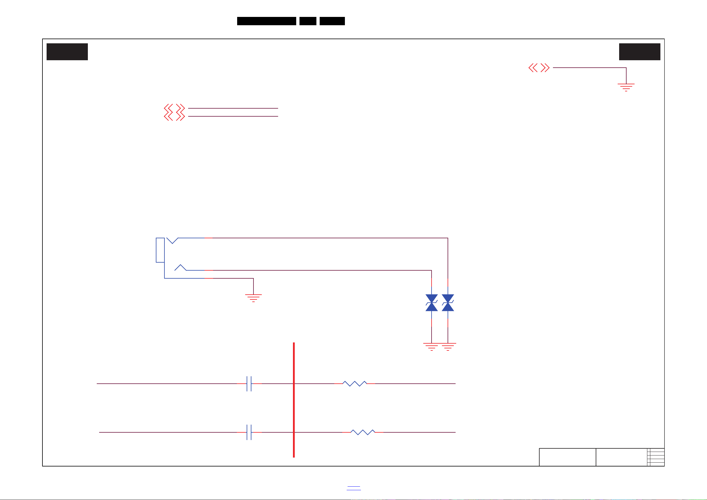
10-3-7 DVI Audio IN
19950_512.eps
DVI Audio IN
B07 B07
2015-04-14
715G7049
DVI Audio IN
DVI_AudioLIN
DVI_AudioRIN DVI_R_IN
DVI_L_IN
CN104
PH ON E J AC K
1
2
3
DVI_AudioLIN
DVI_L_IN
DVI_R_IN
R1034
30Kohm 1/ 16W +/-5%
C1025 1uF 10V
DVI_AudioRIN
R1033
30Kohm 1/ 16W +/-5%
C1024 1uF 10V
GND3,4,5,6,7,8,10,11,12,13,14,15,16,17
DVI_R_IN7
DVI_L_IN7
DVI 1/ 2/3/4 Audi o Input
GND
ZD4105
MLVG0402
1 2
ZD4106
MLVG0402
1 2
Circuit Diagrams and PWB Layouts
EN 54QM16.1L LA 10.
2016-Jul-08
back to
div.table
Page 55
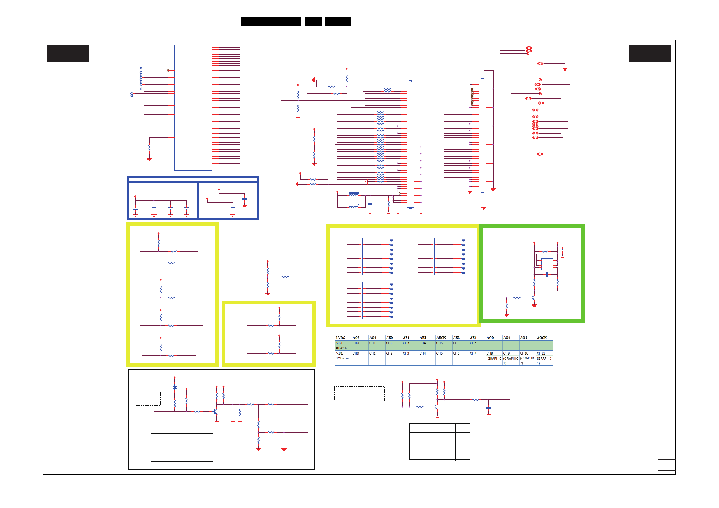
10-3-8 LVDS
19850_513.eps
LVDS
B08 B08
2015-04-14
715G7049
LVDS
B8
R402
NC 1K 1/10W 5%
R405
NC/2KOH M 1/10W
R452 NC/ 47K 1/ 16W 5%
C400
NC/10uF 10V
C
R403
100R 1/10W 5%
R409
4K7 1/16W 5%
R7147&R7148 NC 10K
R7159&R7161 NC 0R
LVDS V-by-1
3D_L/R
R406
1K 1/10W 5%
L/R_IN _to_Panel
+5V_SW
DVDD3V3
3V3SB
DVDD3V3 DVDD3V3
OPC_EN
C4018
NC 100NF 16V
POWER_OK
BL_DIMMING 14
GND3,4,5,6,7,8,9, 11,12,13,14, 15,16,17
3V3SB 3,5,6,7,14,15
INVERTER_ON _OFF 3
BRIGHT_ADJ 3
AVDD3V33,6,7,15
DVDD3V33,5,6,8,11,14,15,16,17
+5V_SW 3,4,6,7,15
R454
NC 0R05 1/16W
R455
NC 0R05 1/16W
R456
NC 0R05 1/16W
R457
NC 0R05 1/16W
R458
NC 0R05 1/16W
R459
NC 0R05 1/16W
R442
NC 100R 1/ 10W 5%
R460
NC 0R05 1/16W
R4315
NC 3K3 1/16W 5%
PANEL_3V3
R461
NC 0R05 1/16W
3D_FORMAT_13D_FORMAT1
C490 100NF 16V
STB_SDA
C492 100NF 16V
C487 100N F 16V
C489 100N F 16V
C488 100N F 16V
C485 100N F 16V
C486 100N F 16V
C491 100NF 16V
R432
0R05 1/16W
V17
V18
V19
V20
V21
V22
V23
V24
B17
B18
B19
B20
B21
LVDSTX_BOC KP
LVDSTX_BO3P
LVDSTX_BO2P
LVDSTX_BO3N
LVDSTX_BOC KN
B22
LVDSTX_BO1N
LVDSTX_BO0N
LVDSTX_BO1P
LVDSTX_BO2N
LVDSTX_BO0P
B23
LVDSTX_BE0 N
LVDSTX_BE1 P
LVDSTX_BE0 P
B24
LVDSTX_BECKP
LVDSTX_BE2 P
LVDSTX_BE3P
LVDSTX_BE2 N
LVDSTX_BECKN
LVDSTX_BO4P
LVDSTX_BE4 P
LVDSTX_BE4 N
LVDSTX_BE3N
LVDSTX_BO4N
B17
C403
100NF 16V
B18
B19
3D_FORMAT_0
B20
B21
B22
B23
R431
10K+-5%1/16W
B24
3D_FORMAT_1
R735
4.7K1/16W
OPC_EN
BL_DIMMING
INVERTER_ON_OFF
BRIGHT_ADJ
LVDSTX_BE1 N
GND
BRIGHT_ADJ
3D_L/R14
3D_L/R
MT 55 9 3UPIJ
U401-3
TCON 0
AL21
TCON 1
AM21
TCON 2
AN22
TCON 3
AM22
TCON 4
AM23
TCON 5
AL22
TCON 6
AL23
TCON 7
AL24
TCON 8
AM24
TCON 9
AN24
TCON 10
AM25
TCON 11
AN25
TCON 12
AL25
AVDD10_LVDS
AU21
AVDD33_LVDSA
L28
REXT_VPLL
AV21
BE0P
AV25
BE0N
AU25
BE1P
AT24
BE1N
AR24
BE2P
AT23
BE2N
AR23
BECKP
AV23
BECKN
AU23
BE3P
AT22
BE3N
AR22
BE4P
AT21
BE4N
AR21
BO0P
AV29
BO0N
AU29
BO1P
AT28
BO1N
AR28
BO2P
AT27
BO2N
AR27
BOCKP
AV27
BOCKN
AU27
BO3P
AT26
BO3N
AR26
BO4P
AT25
BO4N
AR25
AE0P
AV33
AE0N
AU33
AE1P
AT32
AE1N
AR32
AE2P
AT31
AE2N
AR31
AECKP
AV31
AECKN
AU31
AE3P
AT30
AE3N
AR30
AE4P
AT29
AE4N
AR29
AO0P
AV37
AO0N
AU37
AO1P
AT36
AO1N
AR36
AO2P
AT35
AO2N
AR35
AOCKP
AV35
AOCKN
AU35
AO3P
AT34
AO3N
AR34
AO4P
AT33
AO4N
AR33
AVDD33_LVDSB
M28
3D_L/R_IN6, 14
3D_L/R_IN
C407
NC/1uF 10V
WIFI_OCP6
WIFI_OCP
PANEL_3V3
+5V_SW
C409 100NF 16V
PANEL_3V3
PANEL_3V3
PANEL_3V3
PANEL_3V3
CN408
CONN
1
2
3
4
5
6
7
8
9
10
11
12
13
14
15
16
17
18
19
20
21
22
23
24
25
26
27
28
29
30
31
32
33
34
35
36
37
38
39
40
41
42
43
44
45
46
47
48
49
50
51
52
53
54
55
56
57
58
59
60
61
PANEL_3V3
LVDSTX_AO0 N V1
PANEL_3V3
R411
10K 1/8W
R415
NC/0R 05 1/ 16W
R414
NC/47K 1/ 16W 5%
Panel_12V
BIT_SEL
R7163
NC 3K3 1/16W 5%
DVDD3V3
C402
NC/10uF 16V
LVDSTX_BO3P
LVDSTX_BE0 N
LVDSTX_BO1N
LVDSTX_AOC KP
R418
NC/0R 05 1/ 16W
LVDSTX_AE4 P
LVDSTX_AECKP
LVDSTX_AO4P
LVDSTX_AO2N
LVDSTX_BO4N
R413
NC/47K 1/ 16W 5%
LVDSTX_AOC KN
LVDSTX_BO1P
LVDSTX_BOC KP
LVDSTX_BE4 N
LVDSTX_AO0N
LVDSTX_AE2 N
FB401
120R
1 2
FB400
120R
1 2
LVDSTX_BO4P
LVDSTX_BO2N
LVDSTX_BE4 P
LVDSTX_AE3N
LVDSTX_AE0 P
LVDSTX_AE2 P
LVDSTX_AO3N
LVDSTX_BOC KN
LVDSTX_BE2 N
LVDSTX_AE1 N
LVDSTX_AE3P
LVDSTX_BE2 P
LVDSTX_BECKP
LVDSTX_AECKN
LVDSTX_BE0 P
LVDSTX_AO0P
LVDSTX_AO2 P V 6
LVDSTX_AO4P V12
LVDSTX_AO2 N V5
LVDSTX_AO4N V11
LVDSTX_AE4 N
LVDSTX_BO0N
LVDSTX_BE3N
LVDSTX_BO2P
LVDSTX_AO3P
LVDSTX_AOC KP V8
LVDSTX_AO3NV9
LVDSTX_AOCKN V7
LVDSTX_AE0 N V1 3
LVDSTX_AO3PV10
LVDSTX_BO3N
LVDSTX_BECKN
LVDSTX_AE1 P
LVDSTX_BE1 N
LVDSTX_AO1N
LVDSTX_AE2N V17
LVDSTX_AE2 P V 18
LVDSTX_AE1P V16
LVDSTX_AE1N V15
LVDSTX_AE0P V14
LVDSTX_AO2P
LVDSTX_AE0 N
LVDSTX_BO0P
LVDSTX_BE3P
LVDSTX_AO4N
LVDSTX_AO1P
LVDSTX_AE3NV21
LVDSTX_AE3PV22
LVDSTX_AECKN V19
LVDSTX_AECKP V20
LVDSTX_AE4 N V 23
LVDSTX_AE4P V24
LVDSTX_BE1 P
DVDD3V3
LVDSTX_AO0 P V 2
LVDSTX_AO1 N V3
LVDSTX_AO1 P V 4
PANEL_VCC
R416
NC/0R 05 1/ 16W
I NVERTER _ON_OFF
R410
NC/47K 1/ 16W 5%
RA
TP456
2K
1K
TP463
3V3
INVERTER ON/OFF
RA
TP462
5V
BL_ON/OFF:
Inverter on: Low
Inverter off:
High
Wi-Fi_RESET
TP461
N/C
POWER_OK14
WIFI_OCP
POWER_OK
TP455
N/C
RB
TCON2
2D/3D_EN ABLE
RB
R424
6.8K +-1% 1/16W
AVDD33_LVDSA
TP808
PANEL_VCC_ON/OFF
3D_FORMAT1
TP815
TP459
3D_FORMAT0
TP464
REXT_VPLL
AVDD10_LVDS
TP814
LVDS_SEL
R407 0R05 1/16W
PANEL_VCC_ON /OFF4,17
PANEL_VCC_ON /OFF
R426
10K+-5%1/16W
R429
100R 1/16W 5%
L/R_OUT
R7164
NC 0R05 1/ 16W
C408
NC 10UF 10V
AVDD3V3
PANEL_VCC_ON /OFF
R540
NC/0R 05 1/ 16W
R440
6K8 1/16W 5%
R771
10K 1/16W 5%
R772
10K
V1
R773
10K 1/16W 5%
C501
1UF 10% 16V
Q758
BC847C
PANEL_3V3DVDD3V3
R661 0R05 1/16W
AVDD3V3
AVDD33_LVDSB
AVDD1V0 3,6,15
AVDD1V0
C405
1uF 10V
AVDD33_LVDSB
LVDS R423~R439 mounted
V-by-1 C409~C416 mounted
LVDS R663~R670 mounted
V-by-1 C738~C741 mounted
V-by-1 C780~C783 mounted
OPC
D633
NC/BAS316
A
1
K
2
V-by-1: 100N / LVDS: 0R
R7159
0R05 1/16W
R401
NC/4K7 1/ 16W 5%
HTPDN_OUT
BL_ON/OFF
B1
C404
NC 100NF 16V
LVDS_SEL
BL_DIMMING(PW M for BRIGHT_ADJ):
Max: 0V
Min : +3V3
DC
BRIGHT_AD J
10K
100R
PWM
10U
N/C
BL_D IMMI NG
CR
HTPDN
BL_ON/OFF
INVERTER_ON _OFF
BRIGHT ADJUST
L/R_OUT
R7132
NC 0R05 1/ 16W
3D_L/R_IN
C410 100NF 16V
C406
100NF 16V
V2 B2
2D/3D_EN ABLE#
R7133
NC 100R 1/ 10W 5%
R
2D/3D_EN ABLE
R7131
NC 3K3 1/16W 5%
PCID_EN
C522
NC/1UF 10% 16V
R582
NC/0R 05 1/ 16W
2D/3D_EN ABLE#
R666
NC 0R05 1/16W
R665
NC 0R05 1/16W
B11
2D/3D_EN ABLE#
B12
R662 0R05 1/16W
R667
NC 0R05 1/16W
R668
NC 0R05 1/16W
B13
B14
R670
NC 0R05 1/16W
R669
NC 0R05 1/16W
B15
B16
R4294
NC 100K 1%
CN409
NC CONN 41P
1
2
3
4
5
6
7
8
9
10
11
12
13
14
15
16
17
18
19
20
21
22
23
24
25
26
27
28
29
30
31
32
33
34
35
36
37
38
39
40
41
42
43
44
45
46
47
48 49
50
51
L/R_IN _to_Panel
B11
B10
V15
V10
C780100NF 16V
C741 100NF 16V
V13
V14
3V3SB
C782100NF 16V
PANEL_3V3 SW
C738 100NF 16V
B9
B13
B15
V12
C740 100NF 16V
B16
C783 100NF 16V
V11
V16
R4295
NC 100K 1%
C739100NF 16V
C781100NF 16V
NEW
PANEL_3V3
B12
B14
V9
Wi-Fi_RESET
Wi-Fi_RESET6
Q4020
SM3201PSQA-TRG
D
1
D
2
D
3
G4S
5
D
6
D
7
D
8
R425
NC 0R05 1/16W
R423
NC 0R05 1/16W
2D/3D SETUP
C411 100NF 16V
C412 100NF 16V
V4
B3V3
LOCKN
R7161
0R05 1/16W
B4
LOCKN_OUT
R7148
10K+-5%1/16W
PANEL_3V3
R421
NC 0R05 1/16W
R422
NC 0R05 1/16W
LOCKN_OUT
HTPDN14
HTPDN
TP1201
1
R444
NC 0R05 1/16W
R453
0R05 1/16W
R445
100R 1/10W 5%
2D/3D
HTPDN_OUT
R663
NC 0R05 1/16W
VB1
8Lane
TP1203
1
R664
NC 0R05 1/16W
TP1202
1
STB_SCL
TP1204
1
STB_SCL5
B9
TP1205
1
TP1206
1
TP1207
1
TP1208
1
B10
AVDD10_LVDS
R470
NC 0R05 1/16W
R471
NC 0R05 1/16W
AVDD3V3
AVDD1V0
AVDD33_LVDSA
Analog Power
Cobra RAV0.3_20120502
TP1209
1
TP1210
1
TP1211
1
TP1212
1
TP1213
1
TP1214
1
TP1215
1
TP1216
1
R7147
10K+-5%1/16W
TP121 7
1
LOCKN14
LOCKN
R430
NC/0R 05 1/ 16W
OPC
R4296
NC 10R 1/ 16W 1%
scaler output to panel
DVDD3V3
LVDS OUTPUT
LVDS R454~R461 m ounted
V-by-1 C485~C492 mounted
R441
NC 100R 1/ 10W 5%
PANEL_3V3
R4314
NC 3K3 1/16W 5%
3D_FORMAT0 3D_FORMAT_0
TP121 8
1
TP121 9
1
TCON9
TP122 0
1
TP122 1
1
TP122 2
1
TP122 3
1
R438
NC 0R05 1/16W
TP122 4
1
R439
NC 0R05 1/16W
C413 100N F 16V
C414 100NF 16V
V6
B5V5
C416 100NF 16V
V7
V8
B7
B6
C415 100NF 16V
B8
R734
NC 4.7K1/ 16W
STB_SCL
STB_SDA5
B1
STB_SDA
B2
B3
B4
Q400
MMBT3904
B5
R404
4K7 1/16W 5%
B6
Q401
MMBT3904
R400
NC 4.7K1/ 16W
R443
1K 1/10W 5%
C401
NC/10uF 10V
B7
R408
4.7K1/16W
Circuit Diagrams and PWB Layouts
EN 55QM16.1L LA 10.
2016-Jul-08
back to
div.table
Page 56
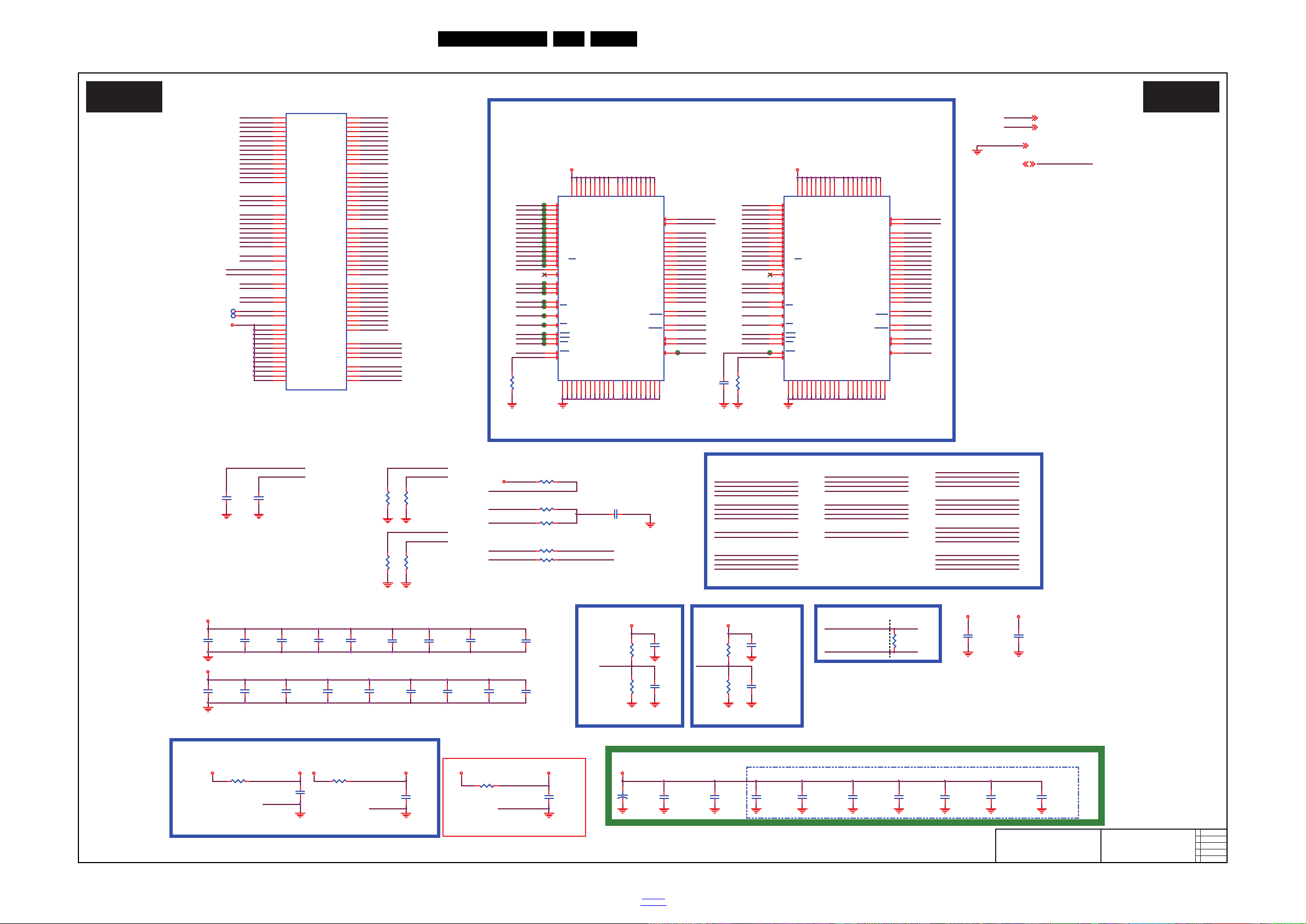
10-3-9 DRAM Interface
19950_514.eps
DRAM Interface
B09 B09
2015-04-14
715G7049
DRAM Interface
R4168
240 OHM +-1% 1/16W
A_RDQS0ARDQS0
A_RDQ14ARDQ14
A_RDQ8ARDQ8
A_RDQ22ARDQ22
A_RDQM3ARDQM3
A_RDQS2ARDQS2
A_RDQS3ARDQS3
DDRVREF_A2
A_RDQ18ARDQ18
A_RDQ20ARDQ20
A_RDQ29ARDQ29
A_RDQ27ARDQ27
ARDQM1 A_RDQM1
A_RDQ16ARDQ16
A_RDQ31ARDQ31
A_RDQ25ARDQ25
ARDQ24 A_RDQ24
A_RDQM2ARDQM2
ARDQ26 A_RDQ26
A_RDQ17ARDQ17
A_RDQ30ARDQ30 A_RDQ12ARDQ12
A_RDQ23ARDQ23
A_RDQ19ARDQ19
C4169
100NF 16V
C4167
100NF 16V
C4168
100NF 16V
C4166
NC 10UF 10V
VCCK3,5,14
VCCK
R433 0R05 1/16W
VCCK
C4172
NC 100NF 16V
AVDD10_DDR
C4193
100NF 16V
C4164
100NF 16V
AVDD10_DDR
C4191
100NF 16V
C4163
100NF 16V
ARCLK0
AVSS_DDR
ARCLK0B
Differential Clock
R427 N C 0R 05 1/ 16W
R434 NC 0R 05 1/ 16W
R4160
1Kohm 1/16W +/-1%
DDRVREF_A1 A_VREFCA1
DDRVREF_A2 A_VREFCA2
AVDD10_DDR
Main Chip Bottom Side
C4179
100NF 16V
C4185
NC 100NF 16V
R4167
240 OHM +-1% 1/16W
C4218
100NF 16V
ARDQS3B
A_RDQS3
C4219
100NF 16V
C4171
100NF 16V
C4192
100NF 16V
C4180
100NF 16V
DDRV
DDRV
DVDD3V3 AVDD33_DDR
DDRV DDRV
AVDD33_DD R
A_VREFCA2A_VREFCA1
DDR3#1 Ref Volt.
AVDD33_DDR
MT5593UPIJ
U401-1
DDRV
AB8
DDRV
AC10
DDRV
AC9
DDRV
AD10
DDRV
AH10
DDRV
AH9
DDRV
AJ10
DDRV
AJ11
DDRV
AJ8
DDRV
AJ9
MEMTP
AE10
MEMTN
AF10
DDRVREF_A1
V1
ARCKE
AA7
ARCLK0
Y4
ARCLK0#
Y5
ARODT
AB6
ARRAS#
AA5
ARCAS#
AA6
ARCS#
AB5
ARWE#
AB7
ARRESET#
AK4
ARBA0
AD5
ARBA1
AE3
ARBA2
AD6
ARCSD#
AB4
ARA14
AM4
ARA13
AK5
ARA12
AF6
ARA11
AK6
ARA10
AD7
ARA9
AH4
ARA8
AL4
ARA7
AJ5
ARA6
AJ6
ARA5
AG7
ARA4
AG5
ARA3
AF4
ARA2
AF7
ARA1
AG6
ARA0
AE4
ARDQM0
AD1
ARDQS0
AC1
ARDQS0#
AC2
ARDQ0
Y2
ARDQ1
AG2
ARDQ2
Y1
ARDQ3
AG3
ARDQ4
W1
ARDQ5
AH3
ARDQ6
W2
ARDQ7
AH2
ARDQM1
AC3
ARDQS1
AD2
ARDQS1#
AE2
ARDQ8
AF1
ARDQ9
AB3
ARDQ10
AG1
ARDQ11
Y3
ARDQ12
AF2
ARDQ13
AB2
ARDQ14
AF3
ARDQ15
AB1
ARDQM2
AN2
ARDQS2
AM3
ARDQS2#
AN1
ARDQ16
AK2
ARDQ17
AT2
ARDQ18
AK1
ARDQ19
AU1
ARDQ20
AJ1
ARDQ21
AU2
ARDQ22
AJ3
ARDQ23
AR4
ARDQM3
AM1
ARDQS3
AP1
ARDQS3#
AP2
ARDQ24
AR2
ARDQ25
AL2
ARDQ26
AT1
ARDQ27
AK3
ARDQ28
AP3
ARDQ29
AL3
ARDQ30
AR3
ARDQ31
AM2
AVDD33_DD R
G1
AVDD10_DD R
AV20
ARTN
W10
ARTP
Y10
DDRVREF_A2
AJ2
TN_HPCPLL
AK18
TP_H PCPLL
AK19
DDRV
AK10
DDRV_CKA
Y6
AVSS_DDR
G2
AVSS_DDR
AU20
DDRV
AK11
AVDD10_DD R
AF13
AVSS_DDR
AF12
AVDD10_DD R
AE19
AVSS_DDR
AE17
TP448 TP
DRAM#2 Bypass Cap
DRAM#1 Bypass Cap
GND 3,4,5,6,7,8,9,10,12,13,14,15,16,17
DVDD3V33,5,6,8,10,14,15,16,17
DDRV 3,12,13
+
C4189
47uF 16V
DDRV
R4150
1Kohm 1/16W +/-1%
C418
100NF 16V
C419
100NF 16V
DDRVREF_A1
DDRVREF_A2
R4166
1Kohm 1/16W +/-1%
C4183
4.7UF 6. 3V
R7127 NC 47K 1/16W 5%
C4170
100NF 16V
ARRESET#
DDRV
C4174
100NF 16V
C4181
100NF 16V
C4178
1UF 10% 16V
AVDD33_DDR
ARDQ21
ARDQ16
ARDQ9
ARDQS0
ARDQ27
ARDQ10
ARDQ7
ARDQ11
ARDQ20
ARDQS0B
ARDQ30
ARDQ13
ARDQM2
C4026
NC 4.7U F 10% 10V
C4025
NC 4.7U F 10% 10V
ARDQ5
ARDQ28
ARDQ4
ARDQ6
ARDQ29
DDRV
ARDQ22
ARDQS2
ARDQ0
ARDQ2
ARDQS1
ARDQ24
ARDQS3B
ARDQ23
ARDQ18
ARDQ14
ARDQ15
ARDQ12
ARDQ3
ARDQM3
ARDQ26
ARDQM0
AVDD10_DDR
ARDQS2B
ARDQ31
ARDQ17
ARDQS1B
ARDQM1
ARDQ8
ARDQ25
ARDQS3
ARDQ1
ARDQ19
DDRV
AVDD10_DDR
Main Chip DE-CAP.
R4107
NC 49.9 OHM 1% 1/16W
R4108
NC 49.9 OHM 1% 1/16W
AVDD10_DDR
DDRV
MEMTN
MEMTP
DVDD3V3
R437 0R05 1/16W
AVDD10_DDR
AVSS33_DDR
C4186
1uF 10V
C4173
100NF 16V
R4152
100R 1/16W 5%
DDRV
U402
NT5CB256M16CP-EK
NC_A15
M7
VSSA9VSSB3VSSE1VSSG8VSSJ2VSSJ8VSSM1VSSM9VSSP1VSSP9VSST1VSST9VSSQB1VSSQB9VSSQD1VSSQD8VSSQE2VSSQE8VSSQF9VSSQG1VSSQ
G9
A13
T3
A12/BC
N7
A11
R7
A10/AP
L7
A9
R3
A8
T8
A7
R2
A6
R8
A5
P2
A4
P8
A3
N2
A2
P3
A1
P7
A0
N3
BA0
M2
BA1
N8
BA2
M3
CK
J7
CK
K7
CKE
K9
CS
L2
RAS
J3
CAS
K3
WE
L3
ODT
K1
RST
T2
ZQ
L8
LDM
E7
UDM
D3
A14
T7
VDDB2VDDD9VDDG7VDDK2VDDK8VDDN1VDDN9VDDR1VDD
R9
VDDQA1VDDQA8VDDQC1VDDQC9VDDQD2VDDQE9VDDQF1VDDQH2VDDQ
H9
DQU7
A3
DQU6
B8
DQU5
A2
DQU4
A7
DQU3
C2
DQU2
C8
DQU1
C3
DQU0
D7
DQL7
H7
DQL6
G2
DQL5
H8
DQL4
H3
DQL3
F8
DQL2
F2
DQL1
F7
DQL0
E3
LDQS
F3
LDQS
G3
UDQS
C7
UDQS
B7
VREF_DQ
H1
VREF_CA
M8
DDRV
AVSS33_DDR
ARA3
ARA2
ARA1
ARA7
ARA6
ARA5
ARA4
ARA0
ARA12
ARA11
ARA10
ARA9
ARA8
ARCAS
ARRAS
ARCS
ARODT
ARWE
ARCKE
ARA14
ARBA0
ARBA2
ARBA1
ARA13
A_RDQ12
A_RDQ11
A_RDQ10
A_RDQ9
A_RDQ8
ARDQS1B
A_RDQS1
A_RDQ0
A_RDQ15
A_RDQ14
A_RDQ13
A_RDQ1
A_RDQM1
A_RDQM0
A_RDQS0
ARDQS0B
AVSS_DDR
A_RDQ6
A_RDQ5
A_RDQ4
A_RDQ3
A_RDQ2
A_VREFCA1
DDRVREF_A2
ARRESET#
A_RDQ7
A_VREFCA2
ARRESET#
A_ZQ2
ARCLK0
A_ZQ1
DDRVREF_A1
MEMTN
ARCKE
ARCLK0B
ARCLK0
ARCLK0B
MEMTP
ARBA0
ARBA1
ARBA2
ARCS
ARODT
ARWE
R4109
47R +-1% 1/16W
ARA4
ARA0
ARA3
ARA2
ARA1
R4110
47R +-1% 1/16W
ARA13
ARA8
ARA7
ARA6
ARA5
ARRAS
ARA14
ARA12
ARA11
ARA10
ARA9
ARCAS
ARTN
A_RDQ18
A_RDQ17
A_RDQ16
C755
NC 15NF 50V
DDR3#1-256Mx16-1866MHz DDR3#2-256Mx16-1866MHz
ARTP
A_RDQ21
A_RDQ20
A_RDQ19
A_RDQM2
A_RDQ24
A_RDQ23
A_RDQ22
A_RDQ26
A_RDQ25
A_RDQM3
A_RDQ31
A_RDQ30
A_RDQ29
A_RDQ28
A_RDQ27
R678
NC 0R05 1/16W
ARTN
ARTP
U403
NT5CB256M16CP-EK
NC_A15
M7
VSSA9VSSB3VSSE1VSSG8VSSJ2VSSJ8VSSM1VSSM9VSSP1VSSP9VSST1VSST9VSSQB1VSSQB9VSSQD1VSSQD8VSSQE2VSSQE8VSSQF9VSSQG1VSSQ
G9
A13
T3
A12/BC
N7
A11
R7
A10/AP
L7
A9
R3
A8
T8
A7
R2
A6
R8
A5
P2
A4
P8
A3
N2
A2
P3
A1
P7
A0
N3
BA0
M2
BA1
N8
BA2
M3
CK
J7
CK
K7
CKE
K9
CS
L2
RAS
J3
CAS
K3
WE
L3
ODT
K1
RST
T2
ZQ
L8
LDM
E7
UDM
D3
A14
T7
VDDB2VDDD9VDDG7VDDK2VDDK8VDDN1VDDN9VDDR1VDD
R9
VDDQA1VDDQA8VDDQC1VDDQC9VDDQD2VDDQE9VDDQF1VDDQH2VDDQ
H9
DQU7
A3
DQU6
B8
DQU5
A2
DQU4
A7
DQU3
C2
DQU2
C8
DQU1
C3
DQU0
D7
DQL7
H7
DQL6
G2
DQL5
H8
DQL4
H3
DQL3
F8
DQL2
F2
DQL1
F7
DQL0
E3
LDQS
F3
LDQS
G3
UDQS
C7
UDQS
B7
VREF_DQ
H1
VREF_CA
M8
AVSS_DDR
TP449 TP
TP_HPCPLL
C4175
100NF 16V
TN_H PC PLL
C4182
100NF 16V
AVSS_DDR
ARBA1
ARBA2
ARBA0
ARCS
ARRESET#
R4118
47R +-1% 1/16W
R4119
47R +-1% 1/16W
C4162
100NF 16V
C4161
100NF 16V
ARCS
ARCSD
C4160
10UF 10V
ARCLK0B
ARCLK0
C4310
NC 1uF 10V
DDR3#2 Ref Volt.
C417
100NF 16V
VCCK
ARA0
R4165
1Kohm 1/16W +/-1%
C4155
100NF 16V
AVDD10_DD R
ARCSD
ARA1
C4188
100NF 16V
ARODT
ARA2
Keep a trace from the GND of Cap to Main Chip
ARCKE
ARA3
ARDQS2B
A_RDQS2
ARRAS
ARA4
ARCAS
ARA5
ARWE
ARA6
ARCLK0
ARCLK0B
ARA7
C4194
100NF 16V
ARA8
DDRVREF_A1
ARA9
AVSS_DDR
DDRV
C4184
NC 100NF 16V
ARA10
ARA11
ARA12
ARA13
ARA14
C4158
100NF 16V
A_RDQS1ARDQS1
A_RDQ21ARDQ21
A_RDQM0ARDQM0
ARDQ13 A_RDQ13
ARDQ6 A_RDQ6
A_RDQ28ARDQ28
ARDQ4 A_RDQ4
ARDQ2 A_RDQ2
ARDQ15 A_RDQ15
ARDQ11 A_RDQ11
A_RDQ3ARDQ3
A_RDQ1ARDQ1
ARDQ0 A_RDQ0
ARDQ9 A_RDQ9
A_RDQ7ARDQ7
A_RDQ10ARDQ10
A_RDQ5ARDQ5
Circuit Diagrams and PWB Layouts
EN 56QM16.1L LA 10.
2016-Jul-08
back to
div.table
Page 57
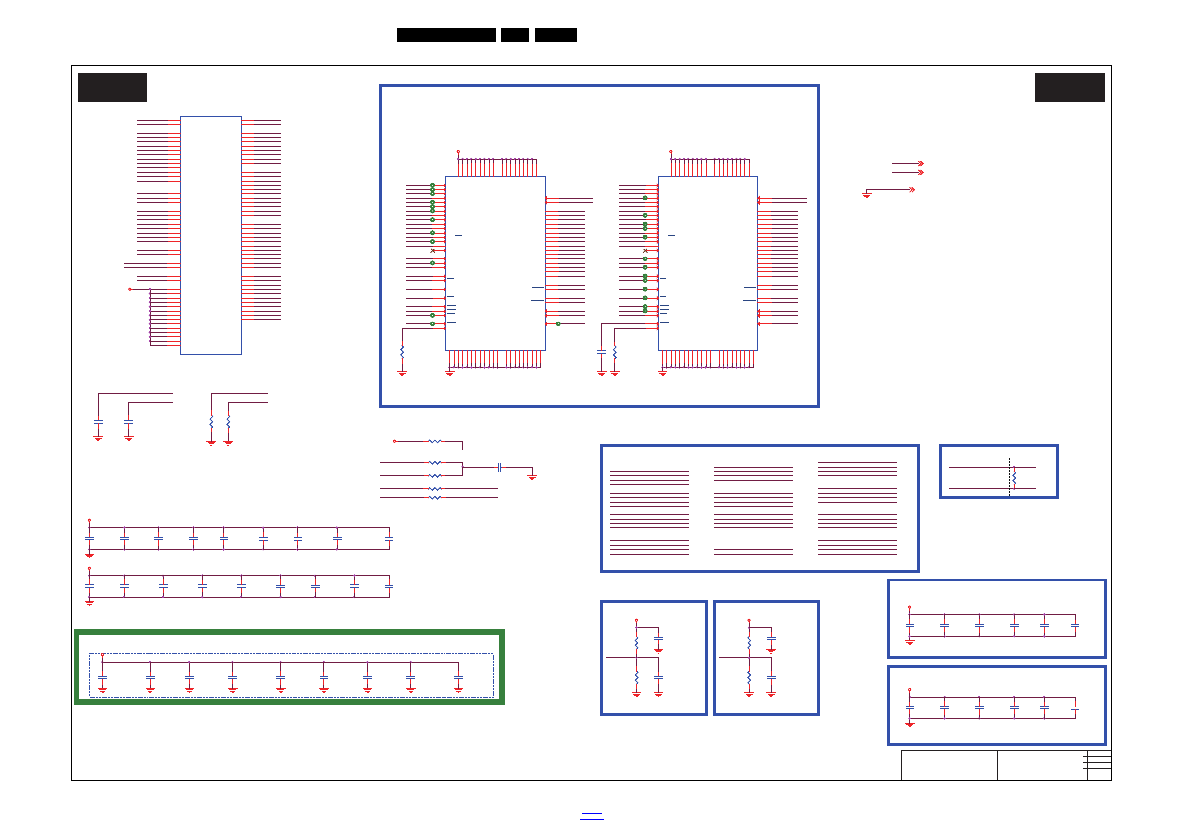
10-3-10 DRAM2 Interface
19950_515.eps
DRAM2 Interface
B10 B10
2015-04-14
715G7049
DRAM2 Interface
BRTN
DDRVREF_B1
DDRVREF_B2
BRTP
R4156
100R 1/16W 5%
B_RCLK0
B_RCLK0#
C452
100NF 16V
Main Chip Bottom Side
DDRV 3,11,13
DDRV
GND 3,4,5,6,7,8,9,10,11,13,14,15,16,17
AVDD3V33,6,7,10,15
AVDD3V3
DDRV
DDR3#3-256Mx16-1866MHz
BRA6
B_RDQ14
B_RDQ20
B_RDQ6
BRCKE
BRA7
B_RDQ23
DDR3#4-256Mx16-1866MHz
B_RDQ9
B_RDQS2
B_RDQ25
BRA11
DDRVREF_B1
R4128
240 OHM +-1% 1/16W
B_RDQ1
B_VREFCA1
BRA3
B_RDQ30
BRA10
BRA2
B_RDQS1#
BRBA2
BRCAS#
BRBA1
B_RDQ22
B_RDQ13
B_RDQ19
B_RDQ5
B_RDQ8
BRCLK0#_D
B_RDQ31
BRODT
MT5593UPIJ
U401-2
DDRVREF_B1
AV2
BRCLK0
AP6
BRCLK0#
AR6
BRCKE
AN9
BRODT
AP9
BRRAS#
AR7
BRCAS#
AP7
BRCS#
AR9
BRBA0
AP11
BRBA1
AN13
BRBA2
AP12
BRWE#
AP10
BRA14
AN18
BRA13
AR17
BRA12
AR13
BRA11
AP17
BRA10
AN10
BRA9
AP16
BRA8
AP18
BRA7
AN16
BRA6
AN17
BRA5
AP14
BRA4
AR15
BRA3
AP13
BRA2
AN14
BRA1
AP15
BRA0
AR12
DDRV
AK12
DDRV
AK13
DDRV
AK14
DDRV
AK15
DDRV
AK16
DDRV
AK17
DDRV
AK7
DDRV
AK8
BRDQM0
AU7
BRDQS0
AU6
BRDQS0#
AT6
BRDQ0
AU4
BRDQ1
AT10
BRDQ2
AU3
BRDQ3
AU10
BRDQ4
AT3
BRDQ5
AU11
BRDQ6
AV3
BRDQ7
AT11
BRDQM1
AV6
BRDQS1
AT8
BRDQS1#
AU8
BRDQ8
AT9
BRDQ9
AU5
BRDQ10
AU9
BRDQ11
AR5
BRDQ12
AV8
BRDQ13
AV5
BRDQ14
AV9
BRDQ15
AT5
BRRESET#
AR18
BRDQM2
AT15
BRDQS2
AV15
BRDQS2#
AU15
BRDQ16
AT13
BRDQ17
AU18
BRDQ18
AU12
BRDQ19
AT18
BRDQ20
AT12
BRDQ21
AT19
BRDQ22
AV12
BRDQ23
AU19
BRDQM3
AR14
BRDQS3
AU16
BRDQS3#
AT16
BRDQ24
AV17
BRDQ25
AT14
BRDQ26
AV18
BRDQ27
AU13
BRDQ28
AU17
BRDQ29
AU14
BRDQ30
AT17
BRDQ31
AV14
BRTP
AL18
BRTN
AL19
DDRVREF_B2
AV11
BRCSD#
AR10
DDRV
AK9
DDRV
AL6
DDRV
AL7
DDRV
AL8
DDRV_CKB
AM8
DDRV
AL9
B_VREFCA2
BRA10
B_RDQ29
BRA5
B_RDQM1
B_RDQS3#
BRA6
DDRVREF_B2
BRA2
DDRV
B_RDQS1
BRA13
BRA9
B_RDQM3
BRA1
BRRAS#
C454
100NF 16V
C456
100NF 16V
DDRV
CAPs for DRAM IO Power ( Close to DDR#3 )
C479
100NF 16V
C483
100NF 16V
C484
NC 100NF 16V
C482
100NF 16V
U404
NT5CB256M16CP-EK
NC_A15
M7
VSSA9VSSB3VSSE1VSSG8VSSJ2VSSJ8VSSM1VSSM9VSSP1VSSP9VSST1VSST9VSSQB1VSSQB9VSSQD1VSSQD8VSSQE2VSSQE8VSSQF9VSSQG1VSSQ
G9
A13
T3
A12/BC
N7
A11
R7
A10/AP
L7
A9
R3
A8
T8
A7
R2
A6
R8
A5
P2
A4
P8
A3
N2
A2
P3
A1
P7
A0
N3
BA0
M2
BA1
N8
BA2
M3
CK
J7
CK
K7
CKE
K9
CS
L2
RAS
J3
CAS
K3
WE
L3
ODT
K1
RST
T2
ZQ
L8
LDM
E7
UDM
D3
A14
T7
VDDB2VDDD9VDDG7VDDK2VDDK8VDDN1VDDN9VDDR1VDD
R9
VDDQA1VDDQA8VDDQC1VDDQC9VDDQD2VDDQE9VDDQF1VDDQH2VDDQ
H9
DQU7
A3
DQU6
B8
DQU5
A2
DQU4
A7
DQU3
C2
DQU2
C8
DQU1
C3
DQU0
D7
DQL7
H7
DQL6
G2
DQL5
H8
DQL4
H3
DQL3
F8
DQL2
F2
DQL1
F7
DQL0
E3
LDQS
F3
LDQS
G3
UDQS
C7
UDQS
B7
VREF_DQ
H1
VREF_CA
M8
B_RDQ18
BRCLK0_D
BRWE#
B_RDQ12
BRCS#
BRA9
BRA14
BRA4
BRRESET#
B_ZQ1
BRRESET#
B_RDQ28
BRA1
B_RDQM0
B_RDQ4
U405
NT5CB256M16CP-EK
NC_A15
M7
VSSA9VSSB3VSSE1VSSG8VSSJ2VSSJ8VSSM1VSSM9VSSP1VSSP9VSST1VSST9VSSQB1VSSQB9VSSQD1VSSQD8VSSQE2VSSQE8VSSQF9VSSQG1VSSQ
G9
A13
T3
A12/BC
N7
A11
R7
A10/AP
L7
A9
R3
A8
T8
A7
R2
A6
R8
A5
P2
A4
P8
A3
N2
A2
P3
A1
P7
A0
N3
BA0
M2
BA1
N8
BA2
M3
CK
J7
CK
K7
CKE
K9
CS
L2
RAS
J3
CAS
K3
WE
L3
ODT
K1
RST
T2
ZQ
L8
LDM
E7
UDM
D3
A14
T7
VDDB2VDDD9VDDG7VDDK2VDDK8VDDN1VDDN9VDDR1VDD
R9
VDDQA1VDDQA8VDDQC1VDDQC9VDDQD2VDDQE9VDDQF1VDDQH2VDDQ
H9
DQU7
A3
DQU6
B8
DQU5
A2
DQU4
A7
DQU3
C2
DQU2
C8
DQU1
C3
DQU0
D7
DQL7
H7
DQL6
G2
DQL5
H8
DQL4
H3
DQL3
F8
DQL2
F2
DQL1
F7
DQL0
E3
LDQS
F3
LDQS
G3
UDQS
C7
UDQS
B7
VREF_DQ
H1
VREF_CA
M8
BRA5
BRA13
BRA14
BRCAS#
B_RDQ11
B_RDQS3
BRCLK0#_D
B_RDQ17
B_RDQM2
BRA8
B_RDQ0
BRCKE
B_ZQ2
BRA0
BRODT
B_RDQ27
B_RDQS0
B_RDQ7
BRBA0
B_RDQ3
BRA4
DDRV
BRRAS#
BRA8
BRA12
B_RDQ10
BRBA0
C451
100NF 16V
B_RDQ21
BRA7
BRCLK0_D
B_RDQ24
B_RDQ15
B_RDQS2#
BRWE#
R4127
240 OHM +-1% 1/16W
B_RDQ2
B_RDQ26
BRA0
BRBA1
B_RDQ16
DDRV
BRA3
BRA12
DDRV
BRBA2
BRA11
BRCS#
B_RDQS0#
B_VREFCA1 B_VREFCA2
BRDQM3
BRDQ24
BRDQ7
BRDQM2
BRDQS2
BRDQ26
BRDQS0#
BRDQS3#
BRDQ4
BRDQ0
BRDQS1#
BRDQ21
BRDQ15
BRDQ9
BRDQS3
BRDQ19
BRDQ1
BRDQ6
BRDQ2
BRDQ30
BRDQ23
BRDQM0
BRDQ8
BRDQS2#
BRDQ16
BRDQS0
BRDQ22
BRDQ25
BRDQ27
BRDQS1
BRDQ29
BRDQ13
BRDQ12
BRDQ31
BRDQ10
BRDQ11
BRDQ5
BRDQM1
BRDQ17
BRDQ3
BRDQ14
BRDQ18
R4124
47R +-1% 1/16W
BRDQ20
BRDQ28
BRTP
R4123
47R +-1% 1/16W
BRTN
NEAR DRAM
DDRVREF_B1
R4126 47R +-1% 1/ 16W
DDR3#4 Ref Volt.
R4125 47R +-1% 1/ 16W
BRCSD#
R435 N C 0R 05 1/ 16W
NEAR Main Chip
B_VREFCA2
BRCS#
C422
100NF 16V
B_VREFCA1
R436 N C 0R 05 1/ 16W
DDRVREF_B2
DRAM#3 Bypass Cap
DDR3#3 Ref Volt.
C428
100NF 16V
DDRV
C427
100NF 16V
C426
100NF 16V
DRAM#4 Bypass Cap
C434
100NF 16V
Differential Clock
C424
100NF 16V
C435
NC 100NF 16V
C430
100NF 16V
C436
100NF 16V
C429
NC 100NF 16V
C440
10UF 10V
C433
100NF 16V
DDRV
C423
NC 100NF 16V
C438
100NF 16V
C431
10UF 10V
C439
100NF 16V
C432
NC 100NF 16V
C425
100NF 16V
C437
100NF 16V
R4132
1Kohm 1/16W +/-1%
C448
100NF 16V
C445
100NF 16V
Main Chip DE-C AP.
C450
100NF 16V
C444
NC 100NF 16V
C457
NC 100NF 16V
DDRV
C461
NC 100NF 16V
C443
1UF 10% 16V
C447
100NF 16V
C449
100NF 16V
DDRV
C460
100NF 16V
C441
NC 10UF 10V
C462
100NF 16V
C458
NC 100NF 16V
C446
100NF 16V
C459
100NF 16V
C453
100NF 16V
CAPs for DRAM IO Power ( Close to DDR#4 )
C756
NC 15NF 50V
R7128 NC 47K 1/ 16W 5%
DDRV
BRRESET#
R4130
1Kohm 1/16W +/-1%
BRCLK0_D
BRCLK0#_D
R4129
1Kohm 1/16W +/-1%
C480
100NF 16V
B_RDQ3BRDQ3
B_RDQ8BRDQ8
B_RDQ21BRDQ21
B_RDQS0BRDQS0
B_RDQM3BRDQM3
B_RDQ23BRDQ23
BRDQ4 B_RDQ4
BRDQ11 B_RDQ11
B_RDQ16BRDQ16
B_RDQ29BRDQ29
B_RDQ28BRDQ28
B_RDQ30BRDQ30 B_RDQ12BRDQ12
B_RDQS2#BRDQS2#
B_RDQ7BRDQ7
BRDQ13 B_RDQ13
B_RDQM2BRDQM2
B_RDQS2BRDQS2
B_RDQM0BRDQM0
B_RDQS0#BRDQS0#
B_RDQ1BRDQ1
B_RDQS1#BRDQS1#B_RDQS3#BRDQS3#
B_RDQ31BRDQ31
B_RDQ27BRDQ27
BRDQ26 B_RDQ26
B_RDQS3BRDQS3
B_RDQ18BRDQ18
B_RDQ17BRDQ17
NEAR BRANCH
BRDQ0 B_RDQ0
B_RDQ10BRDQ10
BRDQ2 B_RDQ2
B_RDQ22BRDQ22
B_RDQ14BRDQ14
B_RDQ25BRDQ25
B_RCLK0#BRCLK0#
B_RCLK0BRCLK0
B_RDQ20BRDQ20
BRDQ24 B_RDQ24
B_RDQS1BRDQS1
BRDQ9 B_RDQ9
B_RDQ5BRDQ5
BRDQ15 B_RDQ15
BRDQM1 B_RDQM1
B_RDQ19BRDQ19
BRDQ6 B_RDQ6
BRWE#
BRA9
BRA14
BRBA2
BRA1
BRA13
BRBA0
BRA0
BRA5
BRCSD#
R4131
1Kohm 1/16W +/-1%
BRRAS#
BRA12
BRA4
BRBA1
BRCAS#
BRCKE
BRA11
BRCLK0
BRA3
BRA8
BRRESET#
BRCLK0#
BRA10
BRA2
BRA7
BRCS#
BRA6
BRODT
DDRVREF_B2
C481
100NF 16V
DDRVREF_B1
C420
100NF 16V
Circuit Diagrams and PWB Layouts
EN 57QM16.1L LA 10.
2016-Jul-08
back to
div.table
Page 58
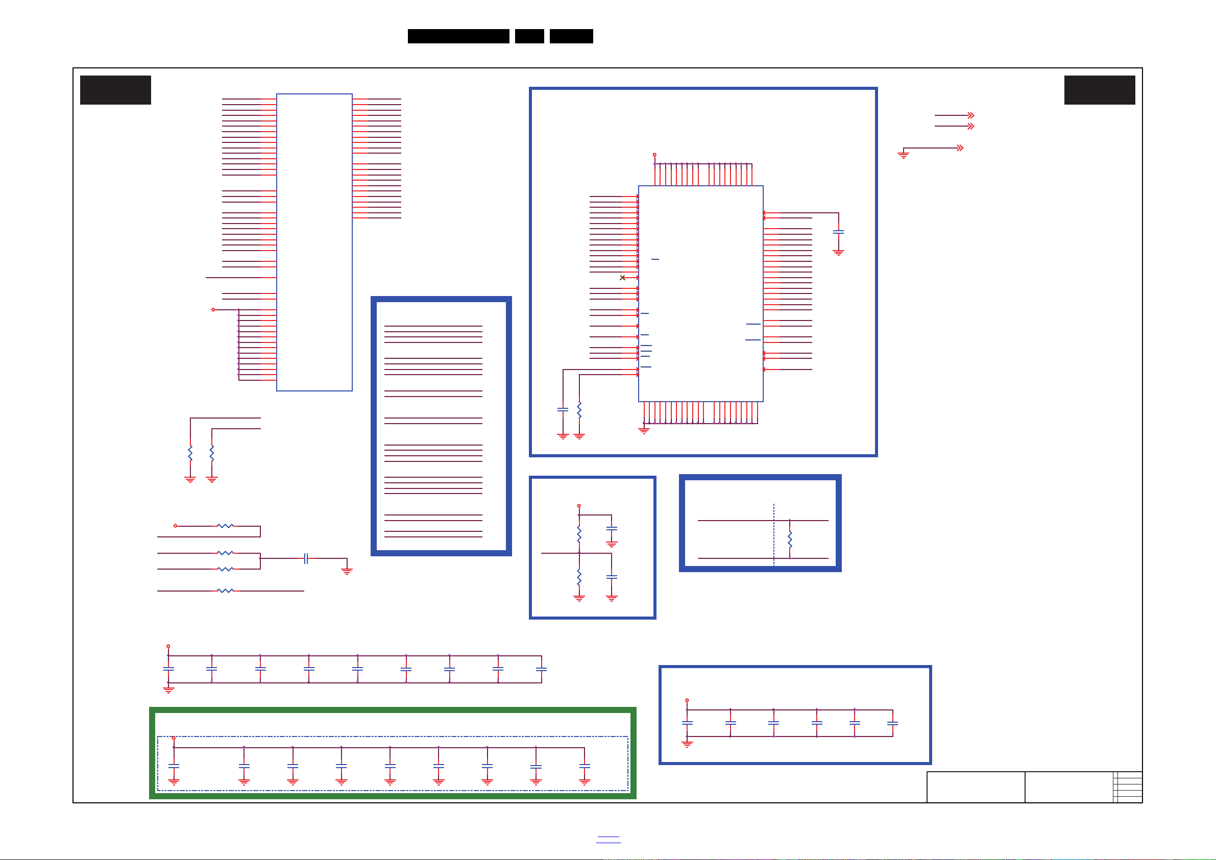
10-3-11 DRAM3 Interface
19950_516.eps
DRAM3 Interface
B11 B11
2015-04-14
715G7049
DRAM3 Interface
CRODT
C_RCLK0#
Damping and Termi natio n fo r CL K
CRDQS0 C_RDQS0
CRCLK0# C_RCLK0#
CRA0
CRDQS1# C_RDQS1#
CRRESET#
C_RDQ5
CRDQ2 C_RDQ2
CRDQ8 C_RDQ8
CRA9
C_RDQ10
CRDQS0# C_RDQS0#
C_RCLK0
CRCS#
C_RDQM0CRDQM0
CRCKE
CRWE#
CRA14
CRDQ13 C_RDQ13
DDRVREF_C1
C421
NC 100N F 16V
CRTN
R4171
NC 47R +-1% 1/16W
CRTP
R4170
NC 47R +-1% 1/16W
CRCS#
DDRVREF_C1
CRCSD#
C_VREFCA1
R4177
NC 47R +-1% 1/16W
R4151
NC 0R 05 1/ 16W
R4178
NC 47R +-1% 1/16W
C4201
NC 100N F 16V
Main Chip Bottom Side
DDR3#5 Ref Volt.
C4195
NC 100N F 16V
C4207
NC 100N F 16V
C4210
100NF 16V
C4213
100NF 16V
C4211
NC 100N F 16V
C4212
NC 100N F 16V
C4214
NC 100N F 16V
R4134
NC 1Kohm 1/ 16W +/ -1%
Main Chip DE-CAP.
DRAM#5 Bypass Cap
DDRV
C467
NC 100N F 16V
C463
100NF 16V
C470
NC 100N F 16V
C469
NC 100NF 16V
C464
NC 100N F 16V
C465
NC 100N F 16V
C471
10UF 10V
C466
NC 100N F 16V
C468
NC 100N F 16V
MT 5593UPIJ
U401-13
DDRVREF_C1
H1
CRCLK0
P4
CRCLK0#
P5
CRCKE
T7
CRODT
L7
CRRAS#
L8
CRCAS#
P9
CRCS#
L5
CRBA0
K5
CRBA1
T4
CRBA2
P7
CRWE#
P8
CRA14
U7
CRA13
H5
CRA12
R4
CRA11
U6
CRA10
T6
CRA9
H8
CRA8
U8
CRA7
H7
CRA6
U9
CRA5
K8
CRA4
U4
CRA3
J4
CRA2
K7
CRA1
U5
CRA0
J5
DDRV
AM5
DDRV
AM6
DDRV
AM7
DDRV
AN4
DDRV
AN5
DDRV
AN6
DDRV
AP4
DDRV
AP5
CRDQM0
N1
CRDQS0
N3
CRDQS0#
N2
CRDQ0
K2
CRDQ1
T2
CRDQ2
J2
CRDQ3
U2
CRDQ4
H2
CRDQ5
V2
CRDQ6
H3
CRDQ7
U1
CRDQM1
M3
CRDQS1
P2
CRDQS1#
P1
CRDQ8
R3
CRDQ9
K3
CRDQ10
R2
CRDQ11
K1
CRDQ12
P3
CRDQ13
L1
CRDQ14
R1
CRDQ15
L2
CRRESET#
H6
CRTP
G3
CRTN
G4
CRCSD#
L6
DDRV
K10
DDRV
L10
DDRV
N10
DDRV
T10
DDRV_CKC
P10
DDRV
U10
C455
NC 100NF 16V
DDRV
DDRV
C_VREFCA1
C478
NC 100NF 16V
DDRV
C472
NC 100N F 16V
C473
100NF 16V
C476
100NF 16V
C474
100NF 16V
C475
100NF 16V
CAPs for DRAM IO Power ( Close to DDR#5 )
C477
100NF 16V
C757
NC 15NF 50V
CRCAS#
CRA7
CRBA2
CRODT
CRTN
CRCLK0
DDRVREF_C1
CRCLK0#
CRA3
CRA13
CRWE#
CRA8
CRBA0
CRA9
CRCS#
CRA1
CRA12
CRCKE
CRA0
CRRESET#
CRA4
CRA5
CRRAS#
CRBA1
CRTP
CRA10
CRCSD#
CRA2
CRA6
CRA11
CRA14
DDRV
CRDQ7
CRDQM1
CRDQ10
CRDQ8
CRDQ11
CRDQS1
CRDQ13
CRDQ1
CRDQ9
CRDQ3
CRDQ5
CRDQ12
CRDQ6
CRDQ4
CRDQS1#
CRDQS0#
CRDQ15
CRDQ14
CRDQ2
CRDQ0
CRDQS0
CRDQM0
DDRV
CRRESET#
R7129 N C 47K 1/ 16W 5%
R4133
NC 1Kohm 1/16W +/ -1%
CRCAS#
CRBA1
GND 3,4,5,6,7,8,9,10,11,12,14,15,16,17
CRCLK0_D
CRA5
CRCLK0#_D
C_RDQ14
CRDQ10 C_RDQ10
CRA10
C_RDQM0
C_RDQ8
CRBA0
C_RDQ3
CRDQ4 C_RDQ4
CRCLK0#_D
CRDQ1 C_RDQ1
DDR3#5-128Mx16-1866MHz
C_RDQ0
C_RDQ6
CRA6
R4192
NC 100R 1/ 16W 5 %
CRDQ11 C_RDQ11
AVDD3V33,6,7,10,15
DDRV 3,11,12
CRA3
C_RDQS0
C_RDQS0#
C_RDQ12
CRDQS1 C_RDQS1
C_RDQS1#
CRBA2
CRRAS#
C_ZQ1
CRDQ14 C_RDQ14
CRA7
CRA1
CRDQ5 C_RDQ5
CRA12
C_RDQ15
CRDQ15 C_RDQ15
CRDQ0 C_RDQ0
R4175
NC 240 OHM +-5% 1/16W
C_RDQS1
C_RDQ7
CRA8
C_RDQ9
CRDQ6 C_RDQ6
C_RDQ11
C_RDQ13
C_RDQM1
C_RDQ12CRDQ12
AVDD3V3
CRA4
CRDQ7 C_RDQ7
CRA2
DDRV
C_VREFCA1
C_RDQ4
C4153
1UF 10% 16V
U406
NC NT5CB128M16FP-EK
NC_A15
M7
VSSA9VSSB3VSSE1VSSG8VSSJ2VSSJ8VSSM1VSSM9VSSP1VSSP9VSST1VSST9VSSQB1VSSQB9VSSQD1VSSQD8VSSQE2VSSQE8VSSQF9VSSQG1VSSQ
G9
A13
T3
A12/BC
N7
A11
R7
A10/AP
L7
A9
R3
A8
T8
A7
R2
A6
R8
A5
P2
A4
P8
A3
N2
A2
P3
A1
P7
A0
N3
BA0
M2
BA1
N8
BA2
M3
CK
J7
CK
K7
CKE
K9
CS
L2
RAS
J3
CAS
K3
WE
L3
ODT
K1
RST
T2
ZQ
L8
LDM
E7
UDM
D3
A14
T7
VDDB2VDDD9VDDG7VDDK2VDDK8VDDN1VDDN9VDDR1VDD
R9
VDDQA1VDDQA8VDDQC1VDDQC9VDDQD2VDDQE9VDDQF1VDDQH2VDDQ
H9
DQU7
A3
DQU6
B8
DQU5
A2
DQU4
A7
DQU3
C2
DQU2
C8
DQU1
C3
DQU0
D7
DQL7
H7
DQL6
G2
DQL5
H8
DQL4
H3
DQL3
F8
DQL2
F2
DQL1
F7
DQL0
E3
LDQS
F3
LDQS
G3
UDQS
C7
UDQS
B7
VREF_DQ
H1
VREF_CA
M8
DDRV
CRA11
C_RDQ2
CRCLK0 C_RCLK0
CRA13
CRDQ9 C_RDQ9
CRDQ3 C_RDQ3
C_RDQM1CRDQM1
C_RDQ1
CRCLK0_D
C4208
NC 10U F 10V
Circuit Diagrams and PWB Layouts
EN 58QM16.1L LA 10.
2016-Jul-08
back to
div.table
Page 59
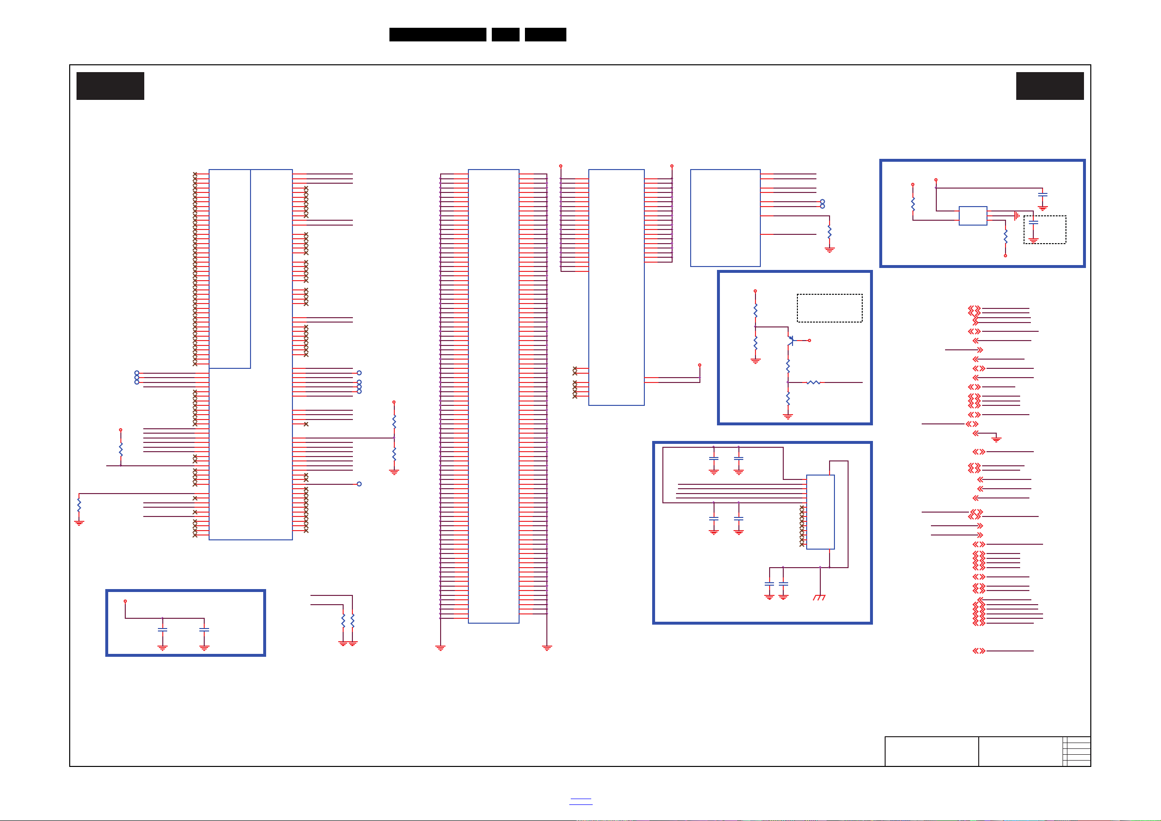
10-3-12 MII/GPIO/ServAD/RJ45
19950_517.eps
MII/GPIO/ServAD/RJ45
B12 B12
2015-04-14
715G7049
MII/GPIO/ServAD/RJ45
2D/3D_SELECT3
2D/3D_SELECT
+5V_SW 3,4,6,7,10,15
+5V_SW
DVDD3V3
R7144
22K 1/16W 1%
Gaming6
Gaming
HP_DET8
HP_DET
HP_DET
R7146
100K 1%
CN4252
RJ45 15P
TCT P 1
1
TD+ P 2
2
TD- P3
3
RD+ P4
4
RD- P5
5
RCT P6
6
NC P7
7
NC P8
8
NC P9
9
NC P10
10
NC P11
11
Y- P12
12
G- P14
14
Y+ P13
13
G+ P15
15
TH1
16
TH2
17
3D_L/R10
3D_L/R
MHL_PWR_EN
BL_DIMMING
Wi-Fi_VCC6
Wi-Fi_VCC
R767
3K3 1/16W 5%
VCC3IO_AB
VCC3IO_B
VCC3IO_A
CVBS_DETECTN
R766
4K7 1/16W 5%
R765
4K7 1/16W 5%
AMBI_TEMP
POWER_OK
KEY_PAD0
R4262
10K 1/16W 5%
DEMOD_TSSYNC16
ARC_SEL_0
ARC_SEL_1
CVBS_DETECTN7
CVBS_DETECTN
DEMOD_TSVALID
DEMOD_TSCLK
DEMOD_TSSYNC
DEMOD_TS0
3D_L/R_IN6,10
DEMOD_TSVALID16
DEMOD_RST
3D_L/R_IN
R7145
0R05 1/16W
R659
4K7 1/16W 5%
3V3SB
SPK_SD
12V_DET :
Normal : High
Power Down : Low
SPK_SD8
SPK_SD
WoBLE-IRQ
WoWLAN_IRQ6
WoWLAN_IRQ
WIFI_PWR_EN
WIFI_PWR_EN6
LED_PWM05,6
ANALOG_DIMMING 3
ANALOG_DIMMING
LED_PWM0
ARC_SEL_1
ARC_SEL_0
WOL_PWR_EN
VCC3IO_SD
DVDD3V3
C4020
100NF 16V
3V3SB
C4021
NC 100N F 16V
VCC3IO_SD
C747
10UF 6. 3V
Gaming
HTPDN
AMBIL_SPI_CLK 17
AMBIL_SPI_CLK
ANALOG_DIMMING
VCC3IO_AB3,5,6,8,10,11,15,16,17
VCC3IO_AB
BL_DIMMING
2D/3D_SELECT
WOL_PWR_EN
DVDD3V3
GPIO0
GPIO1
GPIO2
GPIO3
GPIO4
GPIO5
GPIO6
GPIO7
GPIO8
GPIO9
GPIO10
GPIO11
GPIO12
GPIO13
GPIO14
GPIO15
GPIO16
GPIO17
GPIO18
GPIO19
GPIO20
GPIO21
GPIO22
GPIO23
GPIO24
GPIO25
GPIO26
GPIO27
GPIO28
GPIO29
GPIO30
GPIO31
GPIO32
GPIO33
GPIO34
GPIO35
GPIO36
GPIO39
GPIO40
GPIO38
GPIO37
GPIO41
MT5593UPIJ
U401-8
CI_A0
C1
CI_A1
C2
CI_A2
B1
CI_A3
C3
CI_A4
B2
CI_A5
A2
CI_A6
A3
CI_A7
A4
CI_A8
E11
CI_A9
E12
CI_A10
D13
CI_A11
D12
CI_A12
A5
CI_A13
C9
CI_A14
C8
CI_MCLKI
D11
CI_MIVAL
B6
CI_MISTR T
B8
CI_MDI0
A8
CI_MDI1
A7
CI_MDI2
B7
CI_MDI3
C7
CI_MDI4
B5
CI_MDI5
D10
CI_MDI6
C5
CI_MDI7
B4
CI_D0
F8
CI_D1
E5
CI_D2
D4
CI_D3
F16
CI_D4
E15
CI_D5
E13
CI_D6
C10
CI_D7
E14
CI_MDO0
E6
CI_MDO1
D5
CI_MDO2
C4
CI_MDO3
D15
CI_MDO4
F14
CI_MDO5
B10
OPCTRL0
R34
OPCTRL1
R36
OPCTRL2
R33
OPCTRL3
W35
OPCTRL4
Y34
OPCTRL5
T35
OPCTRL6
N33
OPCTRL7
U35
DEMOD_RST
E20
DEMOD_TSCLK
A14
DEMOD_TSDATA0
D19
DEMOD_TSDATA1
F22
DEMOD_TSDATA2
G22
DEMOD_TSDATA3
H22
DEMOD_TSDATA4
H23
DEMOD_TSDATA5
G23
DEMOD_TSDATA6
F25
DEMOD_TSDATA7
F23
DEMOD_TSSYNC
D20
DEMOD_TSVAL
F20
CI_INT
A10
CI_TSCLK
C14
CI_TSDATA0
C13
CI_TSSYNC
B13
CI_TSVAL
A13
PVR_TSCLK
B12
PVR_TSVAL
D18
PVR_TSSYNC
E17
PVR_TSDATA0
F17
PVR_TSDATA1
G17
SPI_CLK1
C12
SPI_CLK
B11
SPI_DATA
A11
SPI_CLE
C11
OPWM2
AP37
OPWM1
AL30
OPWM0
AP38
SD_D0
D1
SD_D1
E2
SD_D2
E1
SD_D3
F2
SD_CMD
D2
SD_CLK
F3
LED_PWM1
AA32
LED_PWM0
AA33
CI_MDO6
B9
CI_MDO7
D14
GPIO42
D3
GPIO43
G16
GPIO44
D17
GPIO45
F5
GPIO46
E4
GPIO47
B3
GPIO48
F4
GPIO49
AK25
GPIO50
AL27
GPIO51
AM27
GPIO52
AN27
GPIO53
AN28
GPIO54
AM28
GPIO55
AL28
OPCTRL8
R35
OPCTRL9
Y33
OPCTRL10
AC35
OPCTRL11
AB37
ADIN0_SRV
L34
ADIN1_SRV
P35
ADIN2_SRV
L35
ADIN3_SRV
E33
ADIN4_SRV
L33
ADIN5_SRV
M33
ADIN6_SRV
J35
ADIN7_SRV
U37
GPIO56
AR37
GPIO57
AU38
GPIO58
AN36
GPIO59
AM36
GPIO60
AK37
GPIO61
E10
GPIO62
E9
GPIO63
D6
GPIO64
C6
GPIO65
E8
GPIO66
D8
VCC3IO_SD
D9
ADIN8_SRV
N35
ADIN9_SRV
N34
OPCTRL12
AC32
OPCTRL13
AG33
OPCTRL14
AE33
OPCTRL15
AD33
OPCTRL16
AD32
OPCTRL17
AC33
OPCTRL18
AD37
OPCTRL19
AD38
OPWM3
AN35
OPWM4
AL36
OPWM5
AM35
OPWM6
AL34
OPWM7
AK35
OPWM8
AK34
LED_PWM2
AF37
LED_PWM3
AG36
OPCTRL20
AD36
TP001
3D_L/R_IN
MT 559 3UPIJ
U401-10
TXVP_0
W37
TXVN_0
W38
RXVN_1
Y38
RXVP_1
Y37
PHYLED1
AA34
PHYLED0
AB35
REXT
V38
AVDD33_ETH
P29
R679
4K7 1/16W 5%
AVDD33_ETH
TP486TP
TP487TP
PHYLED1
PHYLED0
REXT
R4253
24K 1%
3V3SB
TXVP
RXVN
RXVP
TXVN
Q4002
BC857BW
1
23
12V_DET
TP471
TP470
SD_D1
AMBIL_SPI_DO
TP468
SD_CLK
AMBIL_SPI_CLK
SD_CMD
TP472
SD_D3
C4263
0.1uF 25V
C4260
0.1uF 25V
TP831
12V_DET8
12V_DET
LED_PWM0
SYS_EEPROM_WP5
LED_PWM1
ARC_SEL_015
ARC_SEL_115
ARC_SEL_1
ARC_SEL_0
C4258
10NF 50V
C4262
10NF 50V
DEMOD_RST16
DEMOD_RST
C4259
10NF 50V
MT 559 3UPIJ
U401-11
DVSS
AA15
DVSS
AA16
DVSS
AA17
DVSS
AA18
DVSS
AA19
DVSS
AA20
DVSS
AA21
DVSS
AA22
DVSS
AA23
DVSS
AA24
DVSS
AA8
DVSS
AB14
DVSS
AB15
DVSS
AB16
DVSS
AB17
DVSS
AB18
DVSS
AB19
DVSS
AB20
DVSS
AB21
DVSS
AB22
DVSS
AB23
DVSS
AB24
DVSS
AB36
DVSS
AC14
DVSS
AC15
DVSS
AC16
DVSS
AC17
DVSS
AC18
DVSS
AC19
DVSS
AC36
DVSS
AC4
DVSS
AC7
DVSS
AC8
DVSS
AD15
DVSS
AD16
DVSS
AD17
DVSS
AD18
DVSS
AD19
DVSS
AD4
DVSS
AD9
DVSS
AE9
DVSS
AF35
DVSS
AF5
DVSS
AF8
DVSS
AF9
DVSS
AG4
DVSS
AG8
DVSS
AH5
DVSS
AJ36
DVSS
AJ7
DVSS
AK21
DVSS
AK26
DVSS
AK28
DVSS
AL12
DVSS
AL15
DVSS
P19
DVSS
P18
DVSS
P17
DVSS
P16
DVSS
P15
DVSS
N9
DVSS
N23
DVSS
L9
DVSS
M20
DVSS
M21
DVSS
M22
DVSS
M23
DVSS
M31
DVSS
N18
DVSS
N19
DVSS
N20
DVSS
N21
DVSS
P20
DVSS
P21
DVSS
P22
DVSS
P23
DVSS
P24
DVSS
P6
DVSS
R15
DVSS
R16
DVSS
R17
DVSS
R18
DVSS
R19
DVSS
R20
DVSS
R21
DVSS
R22
DVSS
R23
DVSS
R24
DVSS
T15
DVSS
T16
DVSS
T17
DVSS
T18
DVSS
T19
DVSS
T20
DVSS
T21
DVSS
T22
DVSS
T23
DVSS
T24
DVSS
T3
DVSS
T8
DVSS
T9
DVSS
U15
DVSS
U16
DVSS
U17
DVSS
U18
DVSS
U19
DVSS
U20
DVSS
U21
DVSS
U22
DVSS
U23
DVSS
U24
DVSS
U3
DVSS
U32
DVSS
V15
DVSS
V16
DVSS
V17
DVSS
V18
DVSS
V19
DVSS
V20
DVSS
V21
DVSS
V22
DVSS
V23
DVSS
V24
DVSS
W14
DVSS
W15
DVSS
AL5
DVSS
AM10
DVSS
AM11
DVSS
AM12
DVSS
AM13
DVSS
AM15
DVSS
AM16
DVSS
AM17
DVSS
AM9
DVSS
AN3
DVSS
AN7
DVSS
AN8
DVSS
AP21
DVSS
AP23
DVSS
AP24
DVSS
AP26
DVSS
AP27
DVSS
AP28
DVSS
AP29
DVSS
AP31
DVSS
L31
DVSS
W16
DVSS
W17
DVSS
W18
DVSS
AP34
DVSS
AR11
DVSS
AR16
DVSS
AR19
DVSS
AT4
DVSS
AT7
DVSS
B31
DVSS
B33
DVSS
W19
DVSS
W20
DVSS
W21
DVSS
W22
DVSS
W23
DVSS
W24
DVSS
W3
DVSS
W6
DVSS
W8
DVSS
Y14
DVSS
Y15
DVSS
Y16
DVSS
Y17
DVSS
Y18
DVSS
Y19
DVSS
Y20
DVSS
Y21
DVSS
B37
DVSS
C17
DVSS
C19
DVSS
C20
DVSS
E22
DVSS
E26
DVSS
F9
DVSS
G5
DVSS
J3
DVSS
J31
DVSS
Y23
DVSS
Y24
DVSS
Y7
DVSS
Y8
DVSS
J6
DVSS
K6
DVSS
K9
DVSS
F12
DVSS
Y22
TP811
MT 559 3UPIJ
U401-12
VCCK
AA25
VCCK
AA26
VCCK
AA27
VCCK
AB25
VCCK
AB26
VCCK
AB27
VCCK
AC20
VCCK
AC21
VCCK
AC22
VCCK
AC23
VCCK
AC24
VCCK
AC25
VCCK
AC26
VCCK
AC27
VCCK
AD20
VCCK
AD21
VCCK
AD22
VCCK
AD23
VCCK
AD24
VCC3IO_A
F1
VCC3IO_B
AK38
VCCK
AD25
VCCK
AD26
VCCK
AD27
VCCK
AE20
VCCK
AE21
VCCK
AE22
VCCK
AE23
VCCK
AE24
VCCK
AE25
VCCK
AE26
VCCK
AE27
VCCK
V25
VCCK
V26
VCCK
V27
VCCK
W25
VCCK
W26
VCCK
W27
VCCK
Y25
VCCK
Y26
VCCK
Y27
TN_ARMPLL
M14
TP_ARMPLL
N14
NC
A1
NC
A38
NC
AV1
NC
AV38
VCCK
U26
LOCKN
SYS_EEPROM_WP
C4261
100NF 16V
DEMOD_TSCLK16
WoBLE-IRQ
LED_PWM2
WoBLE-IRQ6
AVDD3V33,6,7,10,15
GND3,4,5,6,7,8,9,10,11,12,13,15,16,17
U4601
APL3511CBI-TRG
VOUT
1
GND
2
OCB
3
EN
4
VIN
5
SYS_EEPROM_WP
3D_L/R
KEY_PAD06
BL_DI MMING10
MHL_PWR_EN15
TXVP
TXVN
RXVP
DVDD3V33,5,6,8,10,11,15,16,17
RXVN
AMBIL_SPI_DO 17
3V3SB3,5,6,7,10,15
+12V_AU
DEMOD_TS016
AMBI_TEMP
AMBI_TEMP17
DDR_PWR_EN3
DDR_PWR_EN
LED_PWM25
LED_PWM2
POWER_OK
POWER_OK10
VCCK
R7142
22K 1/16W 1%
DDR_PWR_EN
+12V_AU 3,4
+12V_AU
AVDD33_ETH
C4607
100NF 16V
3V3SB
DEMOD_TSVALID
DEMOD_TS0
DEMOD_TSSYNC
DEMOD_TSCLK
LED_PWM15,6
LED_PWM1
Wi-Fi_VCC
WoWLAN_IRQ
KEY_PAD0
R4266
NC/ 10K 1/ 10W 5%
R4267
10K 1/10W 5%
RJ45
SEPARATE GROUND
WIFI_PWR_EN
HTPDN10
HTPDN
LOCKN10
LOCKN
12V drop detect
MHL_PW R_EN
12V_DET
VCCK
TP482
R7143
15K 1%
AMBIL_SPI_DO
AVDD3V3
3V3SB
VCCK3,5,11
VCCK
Circuit Diagrams and PWB Layouts
EN 59QM16.1L LA 10.
2016-Jul-08
back to
div.table
Page 60
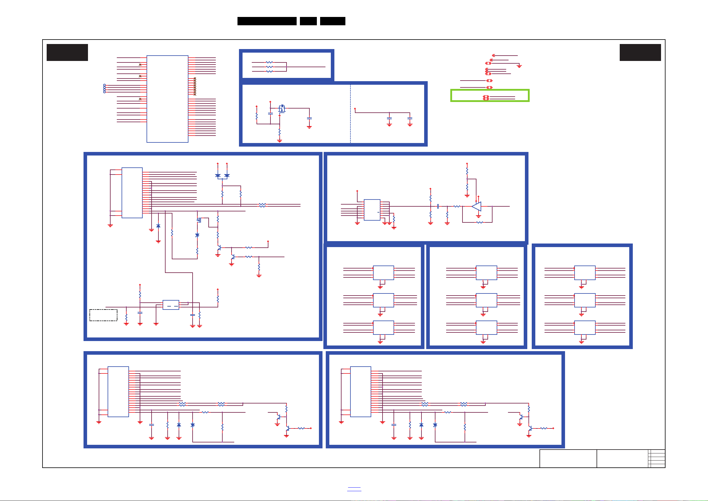
10-3-13 HDMI SW/Connector
19950_518.eps
HDMI SW/Connector
B13 B13
2014-04-14
715G7049
HDMI SW/Connector
HDMI 3 INPUT (Down) FOR HDCP 2.0
RX3_2+
RX3_0-
RX3_0+
RX3_1-
RX3_C+
PWR5V_2
HPD2
PWR5V_3
PWR5V_3
HPD3
PWR5V_2
ZD504NC/PDZ24B
12
R542910R
U514 NC/RClamp0524P.TCT
IN1
1
IN2
2
GND
3
IN3
4
IN45OUT4
6
OUT3
7
GND
8
OUT2
9
OUT1
10
R543
75 OHM +-5% 1/16W
U515 NC/RClamp0524P.TCT
IN1
1
IN2
2
GND
3
IN3
4
IN45OUT4
6
OUT3
7
GND
8
OUT2
9
OUT1
10
R545
100R 1/16W 5%
R546
100R 1/16W 5%
U516 NC/RClamp0524P.TCT
IN1
1
IN2
2
GND
3
IN3
4
IN45OUT4
6
OUT3
7
GND
8
OUT2
9
OUT1
10
D511BAS316
A
1
K
2
R547470K 1/16W 5%
HDMI 3 ESD PROTECTER
C511100NF 16V
(5/7/5)
SDA_3
SCL_3
SMD/ 0402
SMD/ 0402
------><-------
RX2_1-
RX0_1-
RX2_2-
RX2_0+
RX0_C-
RX0_C+
HPD3
RX3_0+
RX3_1+
RX3_C-
RX2_0-
U517 NC/RClamp0524P.TCT
IN1
1
IN2
2
GND
3
IN3
4
IN45OUT4
6
OUT3
7
GND
8
OUT2
9
OUT1
10
RX3_1RX3_2-
RX3_0-
HDMI3_SCL
U518 NC/RClamp0524P.TCT
IN1
1
IN2
2
GND
3
IN3
4
IN45OUT4
6
OUT3
7
GND
8
OUT2
9
OUT1
10
RX2_C-
RX2_C+
HDMI3_SDA
U519 NC/RClamp0524P.TCT
IN1
1
IN2
2
GND
3
IN3
4
IN45OUT4
6
OUT3
7
GND
8
OUT2
9
OUT1
10
RX2_1+
RX3_2+
RX2_2+
RX0_2+
RX0_0-
RX3_C+
RX0_2-
RX0_1+
RX0_0+
RX3_C-
CEC_3
RX3_2-
HDMI 1 ESD PROTECTER
U503
G529A1TB1U
EN(EN)
1
GND
2
IN3OUT
4
OUT
5
OC
6
R428
100K 1/16W 5%
ARC1_HDMI
SDA_2
SCL_2
PWR5V_2
CEC_2
PWR5V_2
SDA_2
SCL_2
CEC_2
RX2_2+
RX2_2-
RX2_1+
RX2_2-
RX2_2+
RX2_1-
RX2_1+
RX2_0+
RX2_C-
RX2_C+
RX2_0-
RX2_0+
RX2_1-
RX2_C-
RX2_C+
RX2_0-
R533
180R
R552
NC/0R 05 1/ 16W
ARC2_HD MI
ZD503NC/PDZ24B
12
R511
33R 1/16W 5%
ZD501
BAT54
13
R536
NC 4K7 1/16W 5%
Audio Return Channel ( ARC)
CN501
HDMI
SHLD0
20
SHLD1
21
TMDSD2+
1
DSHLD0
2
TMDSD2-
3
TMDSD1+
4
DSHLD1
5
TMDSD1-
6
TMDSD0+
7
DSHLD2
8
TMDSD0-
9
TMDSC+
10
CSHLD0
11
TMDSC-
12
CEC
13
NC
14
SCL
15
SDA
16
DDC_GND
17
VCC5
18
HPD
19
SHLD2
22
SHLD3
23
MHL_ PWR _EN
R523910R
C513
NC 1UF 6. 3V
R522
75 OHM +-5% 1/16W
R531
100R 1/16W 5%
C500
100NF 16V
D505BAS316
A
1
K
2
R504 100R 1/16W 5%
R526
100R 1/16W 5%
D510BAS316
A
1
K
2
R530470K 1/ 16W 5%
R505 100R 1/16W 5%
R510
820R
R509
10K 1/16W
R537
0R05 1/16W
C508
1uF 10V
U512
74LVC1G125GV
24
5
1
3
DVDD3V33,5,6,8,10,11,14,16,17
3V3SB
R534
47K 1/16W 5%
ARC7
3V3SB 3,5,6,7,10,14
GND3,4,5,6,7,8,9, 10,11,12,13, 14,16,17
ARC
R535
82R
AVDD3V3
DVDD3V3
AVDD3V33,6,7,10
AVDD1V0
C502
100NF 16V
C509100NF 16V
+5V_SW3,4,6,7,10
GND
+5V_SW
AVDD1V03,6,10
ARC3_HDMI
DVDD3V3
DVDD3V3
Q4001
AO3414
AVDD3V3
(5/7/5)
AVDD1V0
SCL_0
SMD/0402
SMD/0402
SDA_0
R574
100R 1/16W 1%
R544
300K
All HDMI 5V needs 10mils
Q402
MMBT3904
All HDMI 5V needs 10milsAll HDMI 5V needs 10mils
C510
10UF 10V
C507
10UF 10V
R548
10K 1/16W 5%
Q501
AO3401A
AVDD33_HD MI
ARC
R549
0R05 1/10W
AVDD10_HD MI
HDMI_CEC
+5V_SW
DVDD3V3
+5V_SW
D506
BAT54C
3
1
2
+5V_SW
R508
10K 1/16W 5%
ARC_SEL_0
ARC_SEL_014
ARC_SEL_114
ARC_SEL_1
R4037
47K 1/16W 5%
HPMI_0_HPD_C BUS
30mil
50mil
H:MHL ON
L:MHL OFF
+5V_SW
MHL_PWR_EN
CN503
HDMI
SHLD0
20
SHLD1
21
TMDSD2+
1
DSHLD0
2
TMDSD2-
3
TMDSD1+
4
DSHLD1
5
TMDSD1-
6
TMDSD0+
7
DSHLD2
8
TMDSD0-
9
TMDSC+
10
CSHLD0
11
TMDSC-
12
CEC
13
NC
14
SCL
15
SDA
16
DDC_GND
17
VCC5
18
HPD
19
SHLD2
22
SHLD3
23
R577
47K 1/16W 5%
Q406
MMBT3904
Q403
MMBT3904
Q407
MMBT3904
3V3SB
R578
47K 1/16W 5%
HPD2
MHL_ PWR _EN
MHL_PWR_EN14
Analog Power
C746
NC 100NF 16V
SDA_3
SCL_3
CEC_3
PWR5V_3
RX3_0+
RX3_1-
RX3_1+
RX3_2-
RX3_2+
CEC_0
PWR5V_0
RX3_C-
RX3_C+
RX3_0-
RX0_1+
RX0_2-
SDA_0
PWR5V_0
SCL_0
Prevent HDMI leakage from HDMI
device.
RX0_2+
RX0_1-
SDA_0
SCL_0
CEC_0
RX0_2+
RX0_0-
RX0_0+
RX0_1-
RX0_1+
RX0_2-
RX0_C+
RX0_0-
RX0_0+
RX0_C-
RX0_C+
RX0_C-
R7114 47K 1/16W 5%
R550
300K
3V3SB
MHL_ SENSE
ARC_SEL_1
+5V_SW
(5/7/5)
SCL_2
SDA_2
------><-------
ARC2_HDMI
PWR5V_0
R573
20K 1/16W
R554
4K7 1/16W 5%
R7112
47K 1/16W 5%
HDMI 2 INPUT (Down)
R7113
47K 1/16W 5%
HDMI0_SCL
HDMI0_SDA
R539
1K 1/16W 5%
ARC1_HD MI
R7116 47K 1/16W 5%
R7117 47K 1/16W 5%
R7118 47K 1/16W 5%
U521 NC/RClamp0524P.TCT
IN1
1
IN2
2
GND
3
IN3
4
IN45OUT4
6
OUT3
7
GND
8
OUT2
9
OUT1
10
R7119 47K 1/ 16W 5%
U522 NC/RClamp0524P.TCT
IN1
1
IN2
2
GND
3
IN3
4
IN45OUT4
6
OUT3
7
GND
8
OUT2
9
OUT1
10
U523 NC/RClamp0524P.TCT
IN1
1
IN2
2
GND
3
IN3
4
IN45OUT4
6
OUT3
7
GND
8
OUT2
9
OUT1
10
HDMI 4 ESD PROTECTER
PWR5V_3
SDA_3
SCL_3
CEC_3
RX3_0+
RX3_1-
RX3_1+
RX3_2-
RX3_2+
RX3_C-
RX3_C+
RX3_0-
HDMI2_SCL
HDMI2_SDA
PWR5V_2 PWR5V_3
R503 0R 05 1/ 16W
R572 0R05 1/ 16W
R500
0R05 1/16W
CEC_2
CEC_3
MHL_ SENSE
CEC_0
HDMI-CEC
PWR5V_0
MHL_ SENSE
ARC_SEL_0
R579
47K 1/16W 5%
Q408
MMBT3904
Q409
MMBT3904
3V3SB
R580
47K 1/16W 5%
MT5593UPIJ
U401-6
HDMI_CEC
G24
HDMI_0_SCL
F26
HDMI_1_SCL
G30
HDMI_2_SCL
G31
HDMI_3_SCL
D34
HDMI_0_SDA
F27
HDMI_1_SDA
G28
HDMI_2_SDA
F33
HDMI_3_SDA
D33
HDMI_0_PWR5V
G26
HDMI_1_PWR5V
E30
HDMI_2_PWR5V
E31
HDMI_3_PWR5V
E34
HDMI_3_HPD
F34
HDMI_1_HPD
F30
HDMI_2_HPD
F31
HDMI_0_HPD_CBUS
F28
AVDD10_HDMI
A30
HDMI_0_RX_0
A20
HDMI_0_RX_0B
B20
HDMI_0_RX_1
A19
HDMI_0_RX_1B
B19
HDMI_0_RX_2
A18
HDMI_0_RX_2B
B18
HDMI_0_RX_C
A21
HDMI_0_RX_CB
B21
HDMI_1_RX_0
C23
HDMI_1_RX_0B
D23
HDMI_1_RX_1
C22
HDMI_1_RX_1B
D22
HDMI_1_RX_2
A22
HDMI_1_RX_2B
B22
HDMI_1_RX_C
A24
HDMI_1_RX_CB
B24
HDMI_2_RX_0
A26
HDMI_2_RX_0B
B26
HDMI_2_RX_1
C25
HDMI_2_RX_1B
D25
HDMI_2_RX_2
C24
HDMI_2_RX_2B
D24
HDMI_2_RX_C
C26
HDMI_2_RX_CB
D26
HDMI_3_RX_0
C28
HDMI_3_RX_0B
D28
HDMI_3_RX_1
A28
HDMI_3_RX_1B
B28
HDMI_3_RX_2
C27
HDMI_3_RX_2B
D27
HDMI_3_RX_C
C29
HDMI_3_RX_C B
D29
AVDD33_HD MI
P27
MHL_ SENSE
F24
AVDD10_HDMI
B30
AVDD33_HD MI
P28
ARC3_HD MI
TP512 TP
TP511 TP
HDMI0_SCL
AVDD10_HDMI
HPD2
TP513 TP
HPD3
HDMI_0_PWR 5V
AVDD33_HDMI
HDMI2_SDA
HDMI3_SDA
HPMI_0_HPD_C BUS
AVDD10_HDMI
HDMI2_SCL
TP510 TP
HDMI_CEC
HDMI0_SDA
HDMI3_SCL
AVDD33_HDMI
U520
74HC4051PW
Y4
1
Y6
2
Z
3
Y7
4
Y5
5
E
6
VEE
7
GND
8
S2
9
S1
10
S0
11
Y3
12
Y0
13
Y1
14
Y2
15
VCC
16
HDMI 1 INPUT (Sid e) (MHL)
RX2_0+
RX2_1-
RX2_1+
RX2_2-
RX2_2+
CEC_2
RX2_C-
RX2_C+
RX2_0-
RX0_1-
RX0_1+
RX0_2-
RX0_2+
CEC_0
RX0_C-
RX0_C+
RX0_0-
RX0_0+
RX3_1+
CN504
HDMI
SHLD0
20
SHLD1
21
TMDSD2+
1
DSHLD0
2
TMDSD2-
3
TMDSD1+
4
DSHLD1
5
TMDSD1-
6
TMDSD0+
7
DSHLD2
8
TMDSD0-
9
TMDSC+
10
CSHLD0
11
TMDSC-
12
CEC
13
NC
14
SCL
15
SDA
16
DDC_GN D
17
VCC5
18
HPD
19
SHLD2
22
SHLD3
23
Circuit Diagrams and PWB Layouts
EN 60QM16.1L LA 10.
2016-Jul-08
back to
div.table
Page 61
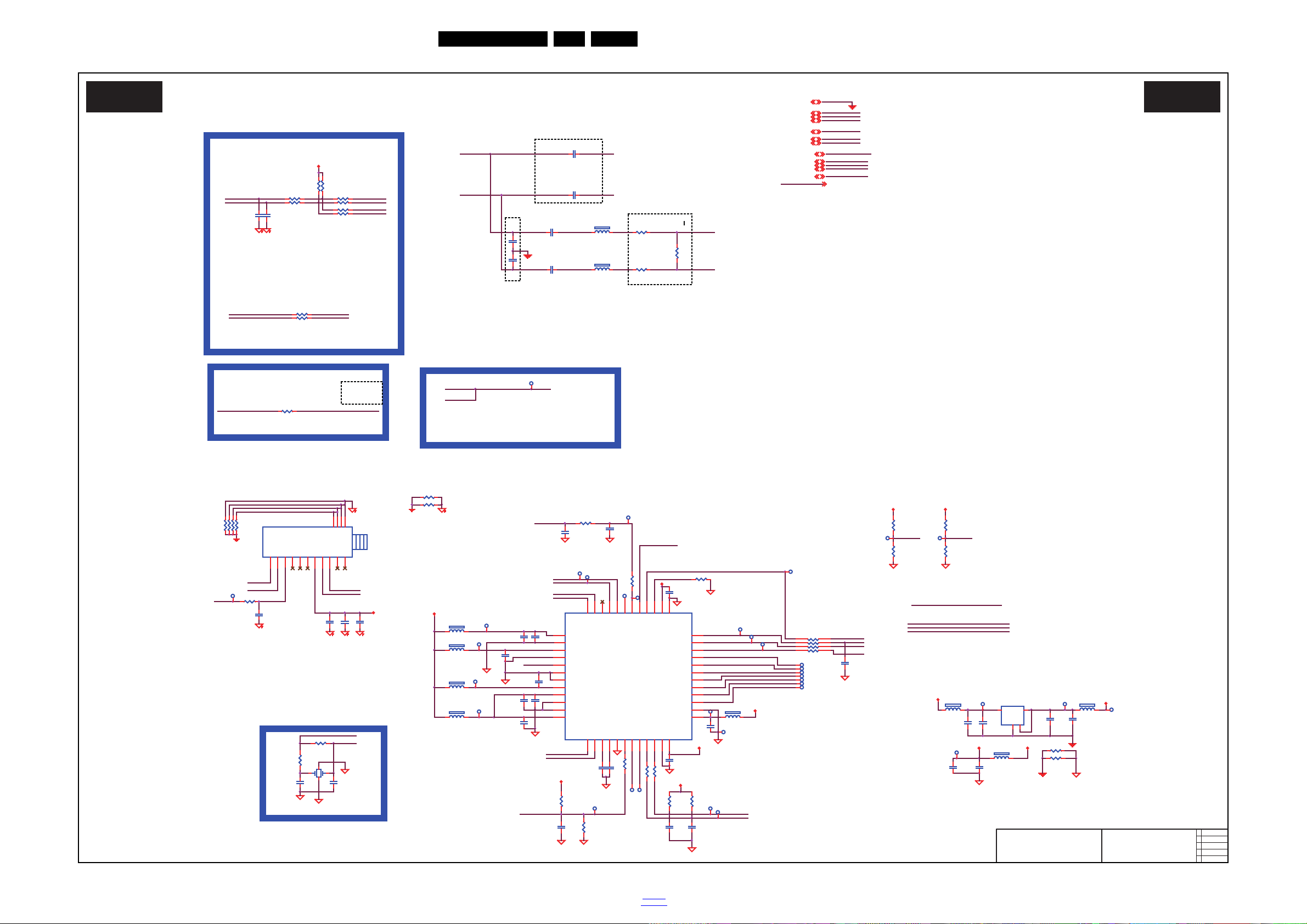
10-3-14 ISDB-T Tuner
19950_519.eps
ISDB-T Tuner
B14 B14
2015-04-14
715G7049
ISDBT Tuner
C4279
10NF 50V
TP733
C4301
27P 50V
C4295
100NF 16V
TP744
TP717
C4284
10UF 6.3V X5R +-20%
R1316
2K 1/16W 5%
C1325
120PF 50V
R7083
0R05 OHM
R1336 0R05 1/16W
C4291
100NF 16V
TP723
TP736
+3V3_TUNER
IF BPF
GND_TunerGND_Tuner
+3V3_TUNER
+3.3VD
Crystal is 16MHZ
+3.3VD
+3.3VD
+3.3VD+3.3VD
+3.3VD
+1V2
+1V2
DVDD3V3 +1V2
DVDD3V3+3.3VD
TU_FAT_IN2-7
TU_FAT_IN2+7
IF_AGC7
OSCL27
OSDA27
GND3,4,5,6,7,8,9,10,11,12, 13,14,15,17
DVDD3V33,5,6,8,10,11,14,15, 17
+3V3_TUNER3
DEMOD_TSVALID14
DEMOD_TSSYNC14
DEMOD_TS014
DEMOD_TSCLK14
DEMOD_RST14
DEMOD_RESET
TS_S2_CLK
TS_S2_DQ0
TUNER
X40 01
16MHz
1243
TU_FAT_IN2+
TU_FAT_IN2-
TS_S2_VALTS_S2_VAL
SBYTE_ORR
TS_S2_SYNC
C4320
NC 10PF 50V
C4321
NC 10PF 50V
DEMOD_RST
FB1022
120R
1 2
FB1023
120R
1 2
XT_O
XT_I
XT_O
XT_I
DEMOD_IFP
DEMOD_IFN
C1072
1uF 10V
GND_Tuner
DEMOD_RESET
R1082
1K
R1081
1K
TUNER_SCL
TUNER_SDA
R1083
NC 200R 1/ 16W 1%
GND_Tuner
GND_Tuner
GND_Tuner
T_IFAGC
DIF_OUT_P
DIF_OUT_N
D_IF_AGC
R7139
0R05 OHM
T_IFAGC
TP238
IF_AGC
DEMOD POWER
DIF_OUT_N
DIF_OUT_P
OSDA2
+3V3_TUNER
DEMOD_SDA
DEMOD_SCL
SLADRS1
SRCK_ORR
PBVAL_ORR
SRDT_ORR
ISDB_T Demodulator
SLADRS0
D_IF_AGC
AGCCNT I
SLADRS1
DEMOD_TSVALID
DEMOD_TSSYNC
DEMOD_TSCLK
OSCL2
R7156
0R05 OHM
R7157
0R05 OHM
GND_Tuner
IF_AGC
OSCL2
OSDA2
TU_FAT_IN2-
TU_FAT_IN2+
ISDB-T TUNER & Demodulator CIRCUIT
AGC
I2C
DEMOD
DEMOD_RESET:
Reset : Low
Normal : High
DEMOD_TS0TS_S2_DQ0
TU101
NC1NC
2
3.3V
5
NC8DIF(P)10DIF(N)
11
SDA3SCL4NC6NC7IF_AGC
9
TH112TH213TH314TH4
15
TS_S2_SYNC DEMOD_TSSYNC
TS_S2_CLK D EMOD_TSCLK
TS_S2_VAL DEMOD_TSVALID
DEMOD
TU_SDA
TU_SCL
SLADRS0
DVDD3V3
DEMOD_TS0
GND_Tuner
DEMOD_RESET
C1071
1uF 10V
C1067
47pF 50V
C1068
47pF 50V
OSDA2
OSCL2
C1065
1uF 10V
C1066
1uF 10V
DEMOD_IFN
DEMOD_SCL
TUNER_SDA
DEMOD_IFP
DEMOD_SDA
Serial TS output
TUNER_SCL
For ISDB-T
TU_SDA
TP731
C4285
100NF 16V
FB4260
120R
12
TP746
C4296
100NF 16V
C4299
10UF 6.3V X5R +-20%
TP725
C4293
10UF 6.3V X5R +-20%
RP4252
33 OHM +-5% 1/16W
1
2
3
4
8
7
6
5
FB4253
120R
12
C4275
100NF 16V
C4280
1uF 10V
C4289
10UF 6.3V X5R +-20%
TP721
R7087
10K 1/10W
TP730
R7096
1.2K OHM
R7095
1M 1/10W 5%
R7104
NC 10K 1/16W 5%
TP713
R7088
NC/ 10K+-5%1/16W
C4283
100NF 16V
C4276
100NF 16V
TU_SCL
R1313
33R 1/10W 5%
C4294
100NF 16V
C0402
TP724
TP729
FB4255
120R
12
R7098
100OHM
TP732
TP740
R1335
0R05 1/16W
TP742
R7089
NC/ 10K+-5%1/16W
FB4254
120R
12
RESET CIRCUIT
C4281
1nF 50V
C4282
470PF 50V
TP727
C4287
100NF 16V
C4288
100NF 16V
R1326 NC/0R 05 1/ 16W
TP712
TP726
TP739
R7090
10K 1/16W 5%
DEMOD_RST
R1308
33R 1/16W 5%
C4302
27P 50V
R7085
0R05 OHM
R7094
47K 1/16W
C4292
100NF 16V
FB4257
120R
1 2
TP737
TP728
TP719
R7091
10K 1/16W 5%
R1303
47R +-1% 1/16W
FB4259
120R
12
R1309
47R +-1% 1/16W
TP714
C4297
100NF 16V
TP734
R7103
4.7K 1/16W
R1302
33R 1/16W 5%
TP743
FB4256
120R
1 2
R1320
2K 1/16W 5%
C4303
10NF 50V
C4300
100NF 16V
R7086
0R05 OHM
U4254
uP0126BJT3-12
VI3VO
2
GND14
4
TP738
R7101
10K 1/16W 5%
C4278
100NF 16V
C4286
NC 10PF 50V
R7102
4.7K 1/16W
R7093
NC 0R05 OH M
TP716
TP745
R7092
20K OHM 1/16W 1%
TP735
TP720
R7100
100OHM
1.2V
U4253
TC90537FG
VSS
47
VDDS
14
GPIO1
4
GPIO2
5
SBYTE
16
AGCCNT1
18
XO
23
SLADRS1
29
PLLVSS
26
SYRSTN42VPGM
41
VDDC
32
ADCVSS
34
VREFH
36
STSFLG143SCL
45
VSS
31
ADCVDD
33
TNSCL
20
TNSDA
21
AINN Q40AINN I38AINP I
37
STSFLG044SDA
46
RSEORF
15
XI
24
VREFL
35
AINP Q
39
SLADRS0
17
CKI
28
VDDC
1
VSS
13
SRCK
12
PBVAL
11
SRDT
10
SLOCK
9
RLOCK
8
RERR
7
SLPEN
6
VDDS
48
VSS
2
GPIO0
3
AGCCNT R
19
XCKO
22
PLLVDD
25
VDDC
27
TSMD
30
TP722
FB4258
120R
12
XTAL
TP715
C4298
100NF 16V
R7099
100R
TP741
R7097
0R05 OHM
R1325 NC/0R 05 1/ 16W
R7084
0R05 OHM
C1326
120PF 50V
C4290
10UF 6.3V X5R +-20%
Circuit Diagrams and PWB Layouts
EN 61QM16.1L LA 10.
2016-Jul-08
back to
div.table
Page 62
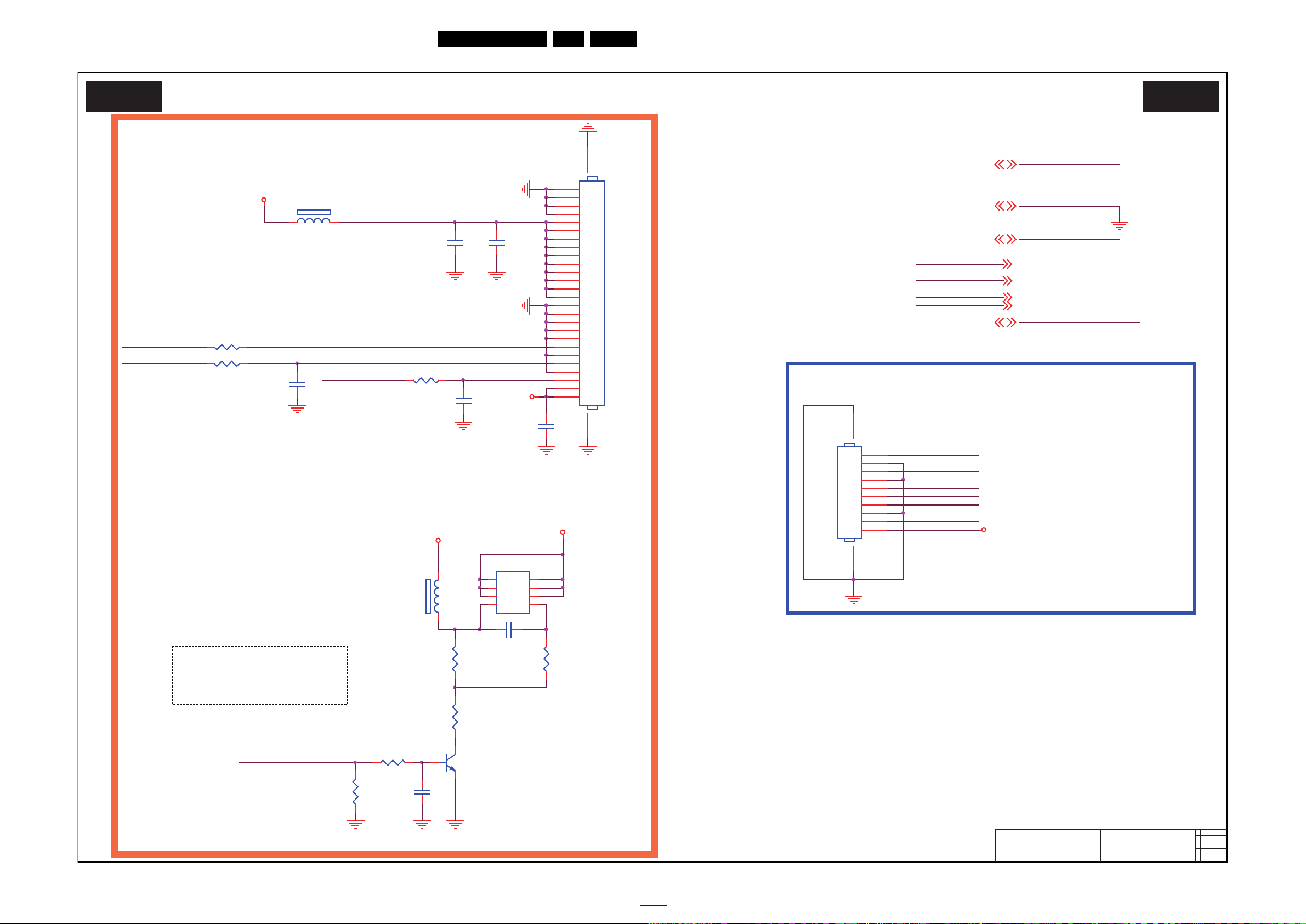
10-3-15 Ambient Light
19950_520.eps
Ambient Light
B15 B15
2015-04-14
715G7049
Ambient Light
FB752
NC 120R
1 2
+12V
C760
NC/4.7UF 10V
R755
NC 10K 1/ 10W 5%
AMBIL_SPI_CLK
AMBIL_SPI_DO
R1401
NC 0R 05 1/ 16W
+12V
+12V_Ambient Light Switch.
PANE L _VCC ON/OF F :(TCON0)
Normal:High
Stand_By:Low
AL+KEY
AMBIL_SPI_DO
R1403
NC 0R 05 1/ 16W
C1405
NC 22PF 50V
Ambient Light
PANEL_VCC_ON/OFF4,10
PANEL_VCC_ON/OFF
DVDD3V3
Key1
Key1 6
Key1
AMBI_TEMP
R1402
NC 0R 05 1/ 16W
AMBIL_SPI_CLK
AMBIL_SPI_CLK
+12V_AMBI
C1400
NC 10UF 16V
FB1402
NC 120R
1 2
C1401
NC 100N F 16V
CN1404
NC CONN
1
2
3
4
5
6
7
8
9
10
11
12
14
15
16
17
18
19
20
21
22
23
24
25
26
2728
13
CN402
CONN
1
2
3
4
5
6
7
8
9
10
1112
C1403
NC 1UF 10% 16V
+12V_AL
DVDD3V3
DVDD3V33,5,6,8,10,11,14,15,16
GND3,4,5,6,7,8,9,10,11,12,13,14,15,16
AMBIL_SPI_CLK 14
AMBIL_SPI_DO 14
+12V3,4,6
AMBI_TEMP 14
AMBI_TEMP
AMBIL_SPI_DO
DVDD3V3
+12V_AMBI
AMBI_TEMP
+12V_AMBI
C1404
NC 22PF 50V
GND
+12V_AL
C759
NC 1UF 10% 16V
Q752
NC BC847C
R757
NC 10K 1/ 16W 5%
R756
NC 5. 1KOH M +-5% 1/10W
PANEL_VCC_ON/OFF
R758
NC 10K 1/ 16W 5%
R754
NC 6K8 1/ 10W 5%
Q753 NC AON4421
D
1
D
2
D
3
G
4
S
5
D
6
D
7
D
8
Circuit Diagrams and PWB Layouts
EN 62QM16.1L LA 10.
2016-Jul-08
back to
div.table
Page 63
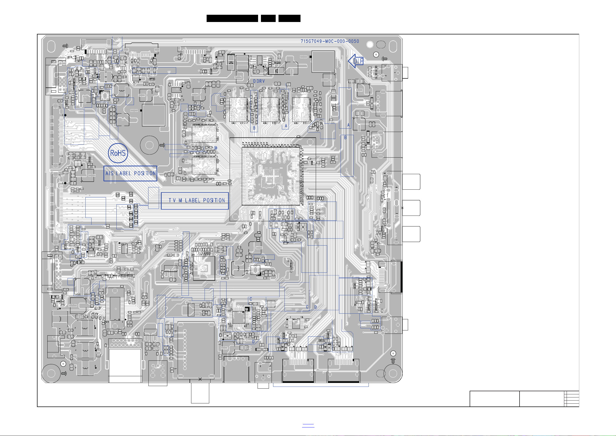
10-3-16 SSB layout top
19950_521.eps
715G7049
LAYOUT TOP
U401
C407
C434
C449
C453
C4162
C4163
C4168
C4313
C4314
C4164
C480
C4167
C470
C474
C476
C1115
C4153
C4026
C1403
C4006
C4315
C1400
C731
C400
C401
CN409CN408
C1039
C1040
C4016
C4022
C4024
C4031
C4035
C4036
C4043
C4044
C4045
C4106
C4107
C4113
C4115
C4117
C4178
C4183
C4247
C4251
C4284
C4289
C4290
C4293
C4299
C443
C501
C5016
C5019
C5020
C5021
C5023
C5024
C5030
C522
C608
C614
C625
C633
C637
C700
C604
C715
C723
C745
C750
C751
C764
C4013
C402
C408
C4160
C4166
C4241
C4242
C4245
C4246
C4250
C4252
C431
C440
C471
C5025
C507
C510
C617
C619
C634
C635
C638
C639
C702
C711
C712
C720
C727
C728
C732
C737
C749
C763
C767
C768
C769
C773
C779
C786
C787
C1080
C4015
C4108
C4111
C4189
C701
C706
C752
C754
C758
C774
C775
FB1001
FB1022
FB1023
FB1402
FB400
FB401
FB4250
FB4253
FB4254
FB4255
FB4256
FB4257
FB4258
FB4259
FB4260
FB603
FB633
FB704
FB705
FB706
FB710
FB712
FB750
FB751
FB754
FB755
L701
L705
L601
L602
L603
L604
R1313
R402
R403
R405
R406
R4102
R4106
R417
R4266
R4267
R4280
R4287
R4291
R4297
R441
R442
R443
R445
R549
R704
R706
R7087
R709
R7095
R7096
R7097
R7133
R7139
R729
R751R752
R753
R4066
R411
R4284
R4289
R4277
R630
R631
D505
D510
D511
D633
ZD4101
ZD4102
ZD503
ZD504
X4000
C643
C644
C736
C645
R4288
R741
C4208
C734
R4202
C771
X4001
C759
C760
FB752
R754
R755
R756
TH4100
TH4101
TH4102
C4019
C4320
C4321
TP1221
H10
TP1216
TP1205
TP1202
TP1201
TP1207
TP1208
TP1204
TP1203
TP1220
TP1219
TP1222
TP1215
TP1224
TP1223
TP1218
TP1217
TP1214
TP1213
TP1212
TP1211
TP1210
TP1209
TP1206
C409
R423
C489
R669
R668
C738
C739
HS401
R4264
R4265
R456
C487
R454
C485
R460
C491
R461
C492
R455
C486
R457
C488
R1011
R424
R4127
R4128
R4168
R4175
R1071
R4129
R4131
R4132
R4130
R435
R436
R4123
R4124
R433
R4001
R4005
C403
C405
C4161
C444
C450
C454
C426
C427
C430
C4312
C452
C433
C438
C436
C439
C445
C446
C437
C447
C448
C481
C4169
C4170
C451
C4171
C4173
C4174
C4179
C4180
C4181
C4182
C4191
C4192
C4195
C4210
C4213
C1010
C4218
C4219
C423
C424
C425
C1325
C472
C473
C475
C4188
C1326
C1067
C455
C459
C460
C461
C463
C464
C465
C466
C467
CN1404
CN104
CN412
CN604
CN501
CN503CN504
CN4102
HS601
C1009
C1024
C1025
C1065
C1066
C1068
C1071
C1072
C1116
C1117
C1401
C1404
C1405
C4004
C4005
C4008
C4009
C4010
C4011
C4012
C4014
C4017
C4018
C4020
C4021
C4023
C4033
C4034
C4037
C4038
C4039
C404
C406
C415
C416
C740
C4116
C741
C4126
C4127
C4128
C4129
C780
C4130
C4131
C781
C411
C4155
C4158
C417
C4172
C4175
C418
C419
C4193
C4194
C420
C4201
C4207
C421
C422
C4244
C4253
C4258
C4259
C4260
C4261
C4262
C4263
C4275
C4276
C4278
C4279
C428
C4280
C4281
C4282
C4283
C4285
C4286
C4287
C4288
C4291
C4292
C4294
C4295
C4296
C4297
C4298
C4300
C4301
C4302
C4303
C4317
C456
C4607
C462
C468
C469
C477
C478
C479
C482
C483
C500
C5010
C5011
C5014
C5015
C5017
C5018
C502
C5022
C5026
C5027
C5028
C5031
C5032
C508
C509
C511
C513
C601
C602
C603
C606
C607
C610
C611
C612
C613
C615
C616
C618
C620
C621
C622
C623
C626
C627
C628
C629
C630
C631
C632
C636
C703
C713
C714
C716
C717
C718
C721
C726
C729
C730
C735
C742
C743
C744
C765
C788
RP4252
CN700
ZD4103
ZD4104
ZD4105
ZD4106
Q4020
Q702
Q750
C766
U4052
L4201
L702
CN402
U702
R1012
R1033
R1034
R1081
R1082
R1083
R1087
R1088
R1302
R1303
R1308
R1309
R1316
R1320
R1325
R1326
R1335
R1336
R4068
R1401
R1402
R1403
R400
R4007
R4009
R401
R4010
R4011
R4013
R4014
R4016
R4017
R4018
R4019
R4020
R4021
R4022
R4023
R4028
R4029
R4030
R4031
R4032
R4033
R4034
R4035
R4036
R404
R4040
R4053
R4054
R4055
R4056
R4057
R4058
R4059
R4060
R4061
R4062
R4063
R4065
R408
R409
R410
R4100
R4104
R4105
R4109
R4110
R4111
R4112
R4114
R765
R4117
R4118
R4119
R412
R4121
R4122
R4125
R4126
R413
R4133
R4134
R4135
R4136
R4137
R4138
R414R415
R4150
R4151
R4152
R4156
R416
R4160
R4165
R4166
R4167
R4170
R4171
R4177
R4178
R418
R419
R4192
R420
R665
R666
R438
R439
R4250
R4251
R4252
R4253
R426
R4262
R4269
R427
R4273
R539
R4064
R4258
R429
R4294
R4295
R4296
R4298
R430
R431
R4314
R4315
R432
R434
R421
R440
R444
R667
R500
R503
R504
R505
R508
R509
R510
R511
R522
R523
R526
R530
R531
R533
R534
R535
R536
R537
R540
R542
R543
R544
R545
R546
R547
R548
R550
R552
R554
R572
R573
R574
R577
R578
R579
R580
R581
R582
R601
R602
R603
R604
R605
R606
R607
R608 R609
R610
R611
R612
R613
R614
R616
R617R618
R619
R620
R621
R622
R623 R624
R625
R626
R627
R628
R629
R633
R634
R635
R636
R637
R660
R701
R702
R703
R705
R707
R708
R7083
R7084
R7085
R7086
R7088
R7089
R7090
R7091
R7092
R7093
R7094
R7098
R7099
R7100
R7101
R7102
R7103
R7104
R7105
R7106
R7107
R7108
R7110
R7112
R7113
R7114
R7116
R7117
R7118
R7119
R712
R7121
R713
R7131
R7132
R714
R7142
R7143
R7144
R7145
R7146
R715
R7155
R7156
R7157
R716
R7163
R7165
R7166
R7167
R7168
R7169
R717
R718R719
R723
R724
R727
R728
R730
R731
R732
R733
R734
R735
R737
R739
R750 R759
R771
R772
R773
U514
U515
U516
U517
U518
U519
U521
U522
U523
D703
D704
U4254
U707
U4250
U512
U4251
U503
Q501
Q706
D4000
D4001
ZD501
Q701
Q751
Q758
Q400
Q401
Q402
Q403
Q406
Q407
Q408
Q409
Q410
Q602 Q603
Q700
U410
Q4001
Q4002
Q604
U701
U706
U520
X1
X2
X3
S2
S3
S1
C410
C412
C413
C414
C782
C783
C762
R4037
R4254
R422
R425
R470
R471
R659
R661
R662
R663
R664
R670
R7127
R7128
R7129
R7147
R7148
R7159
R7161
R766
R767
X5
C746
R428
R4285
R4286
R4290
R671
R672
R673
R4042
U705
C4243
U402
U403
U404
U405
U406
R4278
Q605
R655
R656 R657
R658
R674
R675
R676
R677
Q601
R679
R680
R681
U4601
R437
C4186
C784
C785
R682
R683
R684
R685
R686
R687
R688
Q608
Q606
Q607
CN4100
CN4101
CN4252
X12
X15
X17
CN6005
CN6003
CN600
C709
CN4250
C748
C770
CN401
ZD1101
ZD1102
ZD1103
ZD1104
ZD1105ZD1106
U708
R1072
R4067
R4255
R4256
R4257
R689
R690
R691
R692
R693
R694
R695
R696
R697
R698
R699
R720
R721
U1101
D506
Q4003
Q609
Q753
R757
R758
Q752
U711
U710
U4253
U409
U601
C755
C756
C757
R407
C490
R452
R453
R458
R459
R7164
TU101
C747
R4002
R4003
Circuit Diagrams and PWB Layouts
EN 63QM16.1L LA 10.
2016-Jul-08
back to
div.table
Page 64
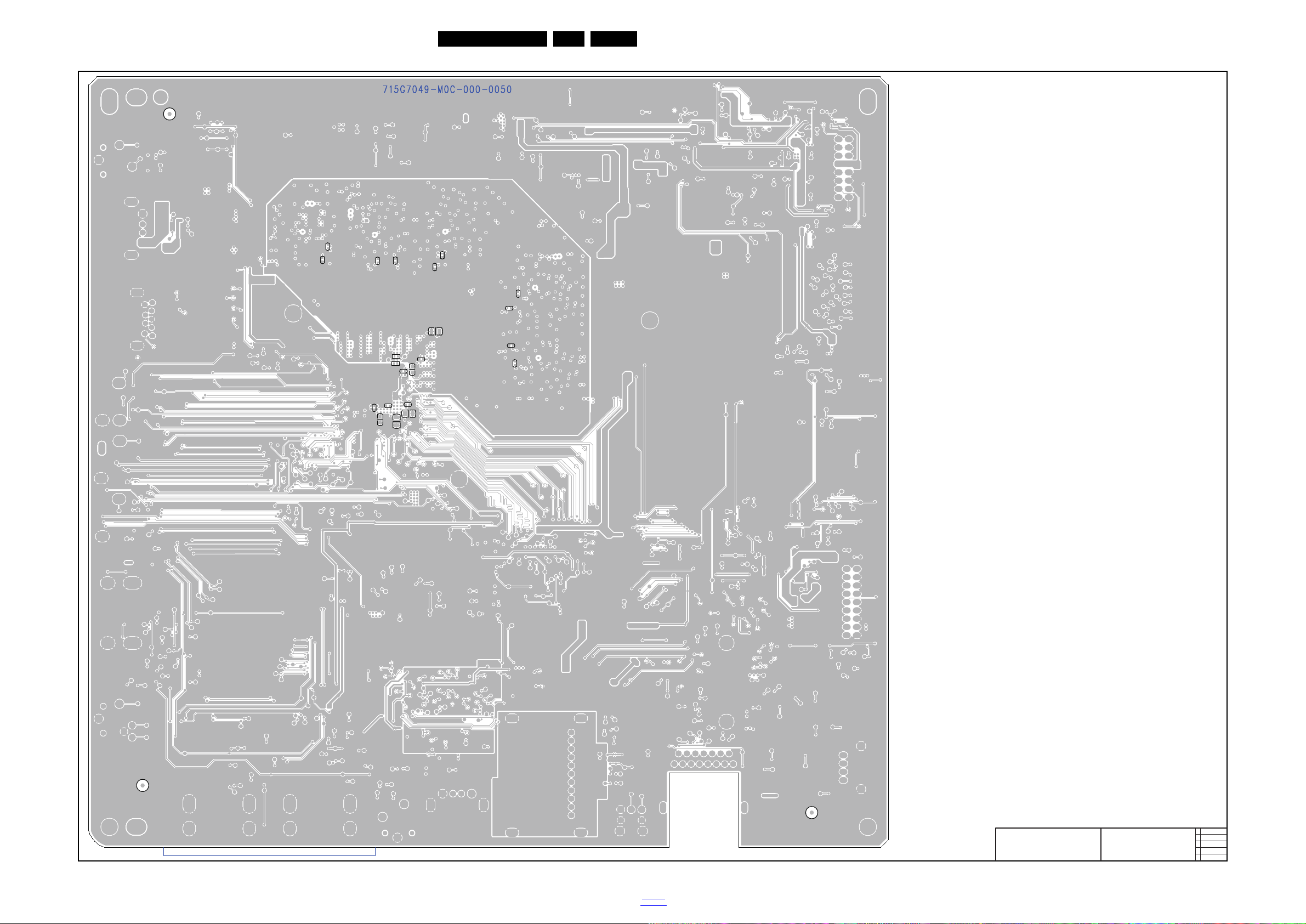
10-3-17 SSB layout bottom
19950_522.eps
715G7049
LAYOUT BOTTOM
C432
C4025
C4027
C722
C733
C441
TP627
TP819
TP482
TP820
TP057
TP058
TP118
TP238
TP285
TP337
TP353
TP604
TP605
TP606
TP607
TP823
TP616
TP617
TP618
TP619
TP620
TP622
TP623
TP624
TP625
TP626
TP712
TP713
TP714
TP715
TP716
TP717
TP719
TP720
TP721
TP722
TP723
TP724
TP725
TP726
TP727
TP728
TP729
TP730
TP731
TP732
TP733
TP734
TP735
TP736
TP737
TP738
TP739
TP740
TP741
TP742
TP743
TP744
TP745
TP746
TP821
TP822
TP825
TP827
TP828
TP824
TP830
TP621
TP826
TP829
TP001
TP74
TP75
TP76
TP80
TP448
TP449
TP450
TP451
TP452 TP453
TP454
TP455
TP456
TP459
TP461
TP462
TP463
TP464
TP468
TP470
TP471
TP472
TP486
TP487
TP510
TP511
TP512
TP513
TP603
TP608
TP609
TP610
TP611
TP612
TP613
TP614
TP700
TP701
TP702
TP703
TP704
TP705
TP706
TP710
TP711
TP808
TP811
TP814
TP815
TP816
TP817
TP818
TP831
R4107
R4108
C4311
C435
C4184
C4185
C4211
C4212
C4214
C457
C458
C429
C4310
C484
C724
C725
R678
X18
X24
X25
Circuit Diagrams and PWB Layouts
EN 64QM16.1L LA 10.
2016-Jul-08
back to
div.table
Page 65
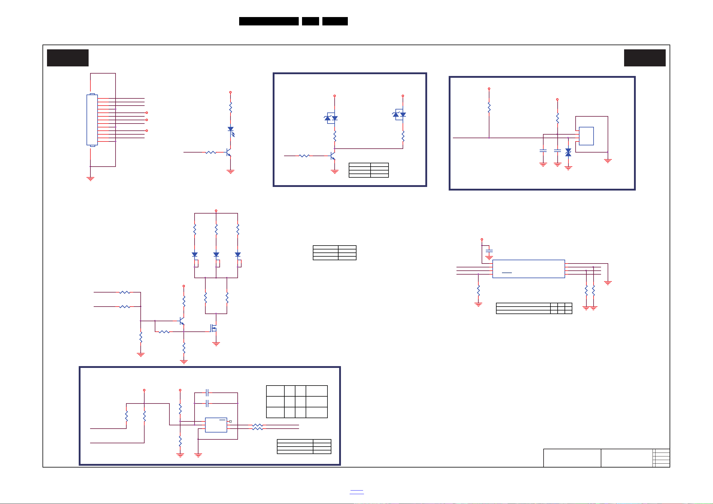
10.4 J 715G7074 IR/LED Panel
19850_526.eps
IR & 3D & Light sensor & LOGO
J J
2014-09-30
C
715G7074
IR &3D&Light sensor&LOGO
R229
0R05 1/16W
R210
10K 1/16W 5%
R211
10K 1/16W 5%
R212
10K 1/16W 5%
C203
1uF 10V
+5V_SW
R219
4.7 OHM +-1% 1/ 10W
R218
10ohm +/-1% 1/ 10W
R217
10ohm +/-1% 1/ 10W
R220
NC/4.7 OHM +-1% 1/10W
C204
1uF 10V
+5V_SW
Standby
LED203
IR LED GPTS12048IRC3-R
12
3
LED204
IR LED GPTS12048IRC3-R
12
3
IR Receiver
3V3SB
R202
100R 1/16W 5%
R201
NC/ 2K7 1/ 16W 5%
3V3SB
RC6
U202
455C
VDD
1
GP5/OSC1/CLKIN
2
GP4/OSC2
3
GP3/MCLR/VPP4GP2/AN2/T0CKI/C1OUT
5
GP1/AN1/C1IN-/ICSPCLK
6
GP0/AN0/C1IN+/ICSPDAT
7
VSS
8
RC6
3D_L/R
3V3SB
LS_SDA
LS_SCL
DVD3V3
Gaming
LED201
GPSS008RC4
12
Red
R204
NC 100R 1/ 16W 5%
R216
10ohm +/-1% 1/ 10W
Active 3D
LOGO
VPP
+5V_SW
3D_L/R
DVD3V3
Wireless_L/R
R207
47K 1/16W 5%
ICSPCLK
ICSDAT
Gaming
3D_L/R
Wireless_L/R
Q202
AO3414
Lighting LOGO
R230
1K 1/16W 5%
R232
2R2 1/16W 5%
DVD3V3
3V3SB
LED205
CHIP LED WHITE 99-113UNC/2223010/TR8
2 1
LED206
CHIP LED WHITE 99-113UNC/2223010/TR8
2 1
R231
2R2 1/16W 5%
3V3SB
LOGO
R205
NC 0R 05 1/ 16W
U203
NC JSA-1130
ADDR
1
VDD
2
GND3SCL
4
SDA
5
INT
6
R213
NC 0R 05 1/ 16W
Light Sensor
R209
NC 10K 1/ 16W 5%
Digital Light Sensor
C202 NC 1uF 10V
R208
NC 10K 1/ 16W 5%
LS_SCL
LS_SDA
R214
NC/ 0R 05 1/ 16W
JSA-1130
R42R41
JSA-1130
NC
NC 0R
0R
I2C addr
R206 NC 0R05 1/ 16W
0x45
0x44
C201 NC 100N 16V
LS_SDA
LS_SCL
DVD3V3
C205
1uF 10V
Q207
BC847BW
MTK 5593 Panel 100/120Hz] NC
A3D Control
R203 U202R204
Yes
Yes YesNC
5500
6200
6500
LOGO Function
NC
Yes
Yes
Q204
NC/BC847BW
NC
R233
1K 1/16W 5%
LED_R
Q201
BC847BW
R215
NC/ 47K 1/ 16W 5%
LED_R
R234
2K2 1/16W 5%
ZD201
MLVG0402
12
5500
6200
6500
Light sensor Function
NC
Yes
NC
5500
6200
6500
A3D function
Yes
NC
NC
U201
TSOP75436TR
GND
1
VCC
2
Vout
3
GND
4
LED202
IR LED GPTS12048IRC3-R
12
3
PIC12F510-I/SN [Panel 50/60Hz]
R203
100R 1/16W 5%
CN201
1
2
3
4
5
6
7
8
9
10
11
12
13
1415
3V3SB
R221
NC/ 10K 1/ 16W 5%
10-4-1 IR & 3D & Light sensor & LOGO
Circuit Diagrams and PWB Layouts
EN 65QM16.1L LA 10.
2016-Jul-08
back to
div.table
Page 66
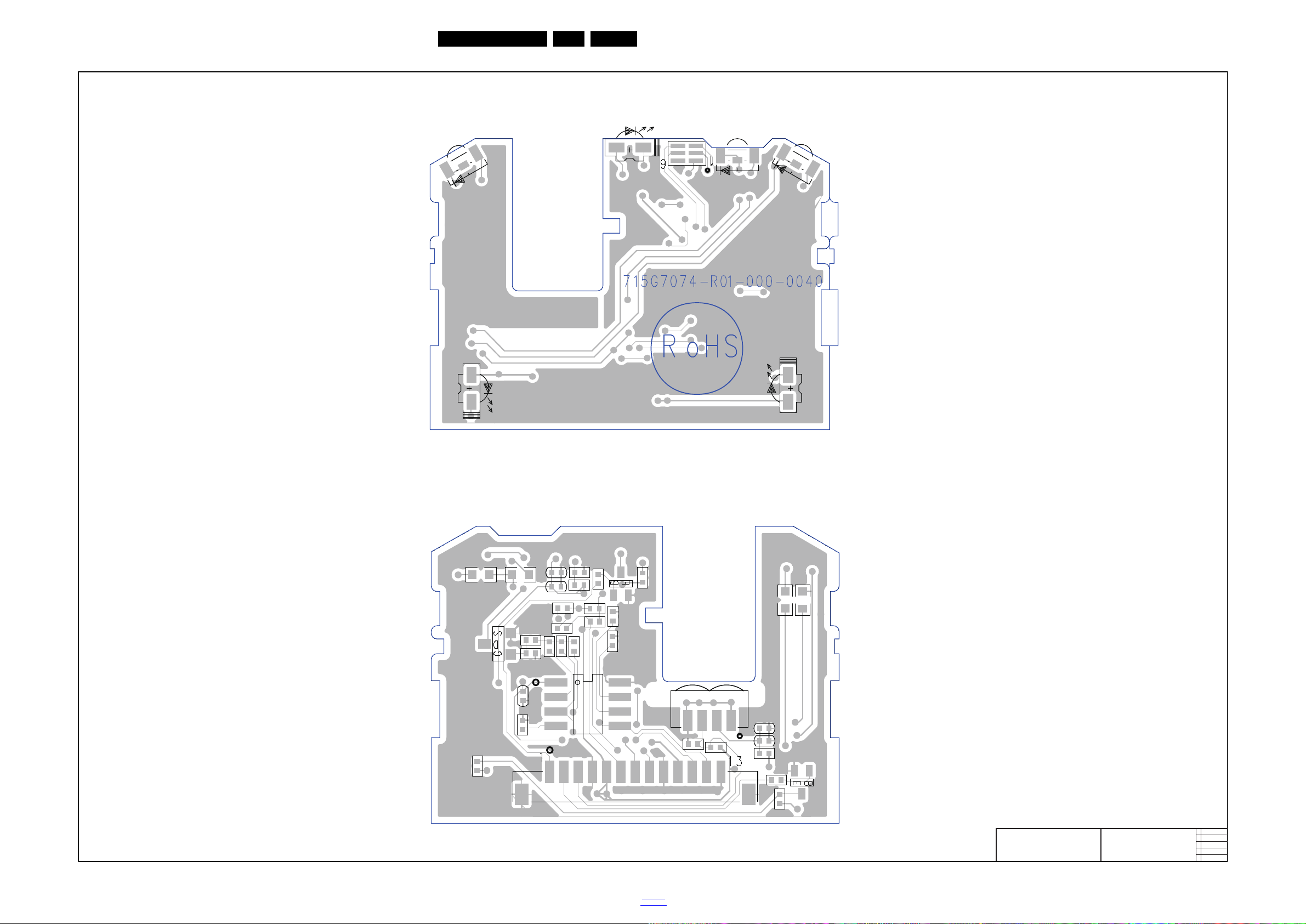
10-4-2 IR/LED board layout
19850_527.eps
715G7074
IR/LED panel
layout top/bottom
LED206
LED201
LED205
U203
LED202
LED203
LED204
R217
R216
R218
R219
R229
Q202
R231
R206
R205
R203
R204
R233
R202
C205
C204
R215
Q207
Q201
R234
R211
R212
U202
C203
R210
R209
R208
CN201
R232
C202
C201
R201
R213
R214
U201
ZD201
R230
R207
Layout IR/LED panel (top side)
Layout IR/LED panel (bottom side)
Circuit Diagrams and PWB Layouts
EN 66QM16.1L LA 10.
2016-Jul-08
back to
div.table
Page 67
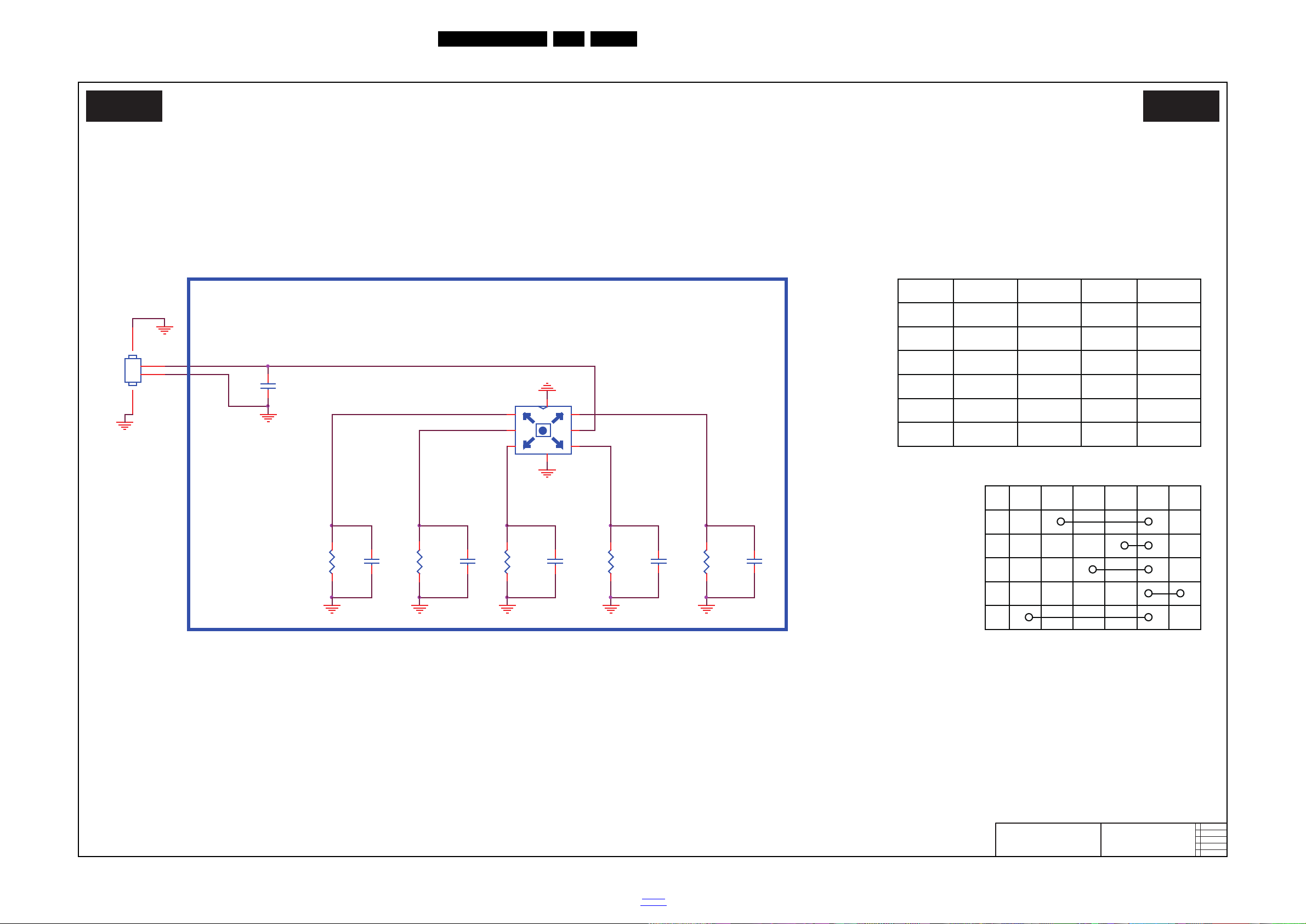
Circuit Diagrams and PWB Layouts
19850_524.eps
Key
E E
2014-05-28
715G7088
Key
KEY1
Menu
Right
Left
Down
Up
6-5 short
R04
2K2 1/10W 1%
2-5 short
F1
3-5 short
R01
1K2 1/10W 1%
1-5 short
4-5 short
F2
F3
F5
F3
F1
F4
F2
SW01
TACT SW 6P
3 4
2
1 6
5
7
8
F4
F5
R05
15K 1/10W 1%
Direction
R03
6K8 1/10W 1%
switch
----><----|
Joystick circuit diagram
C06
0.1uF 50V
pin1
0V
0.5V
0.81V
1.65V
2.27V
pin2
No function
pin3
3.3V
C04
NC / 100N 50V
pin4 pin5
C05
NC / 100N 50V
pin6
----><----|
C01
NC / 100N 50V
C02
NC / 100N 50V
C03
NC / 100N 50V
----><----|
----><----|
----><----|
Down
Up
Center
CN01
CONN
1
2
34
R02
0R05 1/ 10W
0R
2K2
Key functionResistance
Center
CH+
CH-
1K2
VOL-
VOL+
Left
15K
6K8
Right
Voltage
JOYSTICK
10.5 E 715G7088 Keyboard control panel
10-5-1 Key
EN 67QM16.1L LA 10.
2016-Jul-08
back to
div.table
Page 68
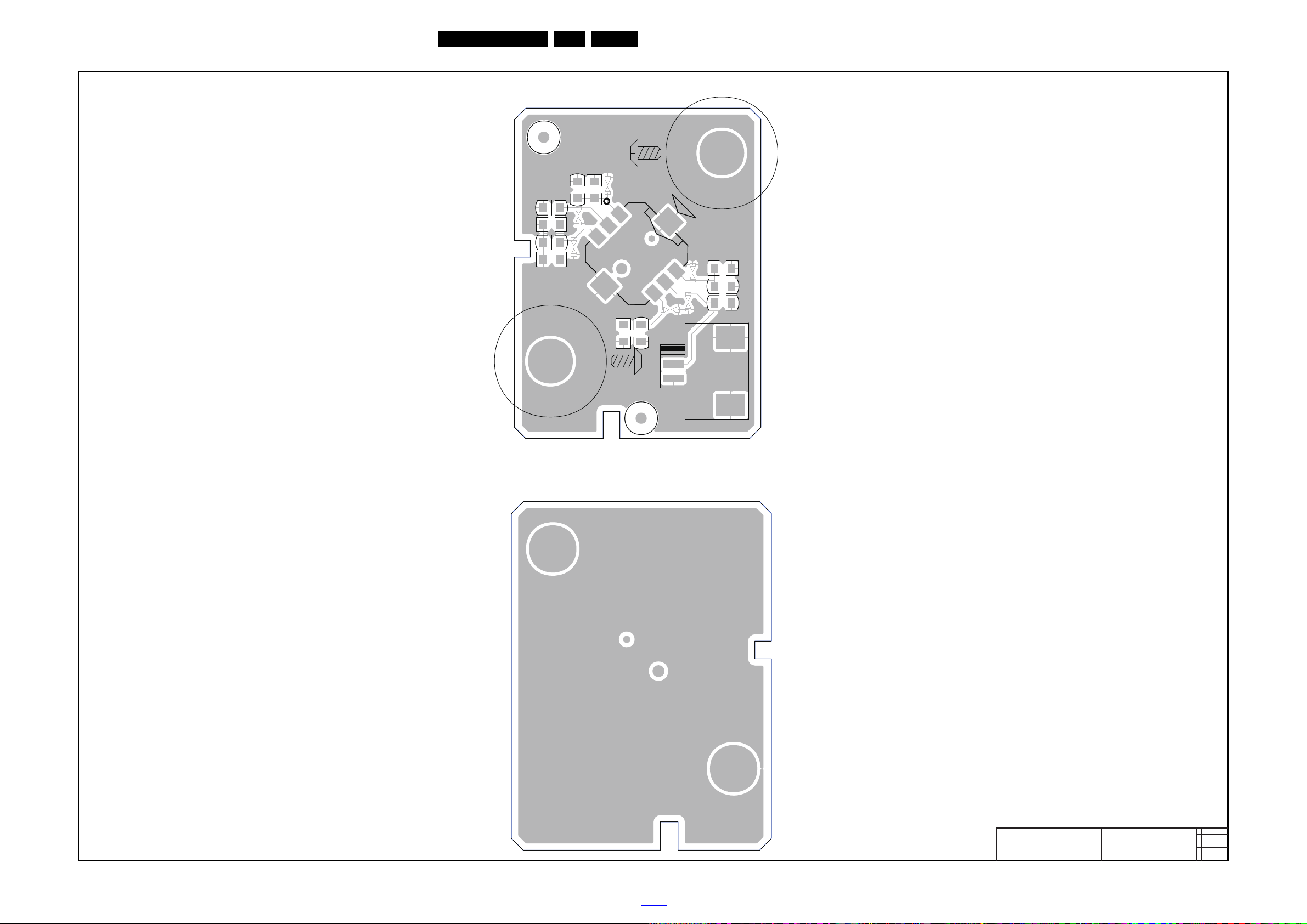
Circuit Diagrams and PWB Layouts
19850_525.eps
2014-06-06
715G7088
Keyboard control panel
layout top/bottom
C01
C02
C03
C04
C05
C06
R01
R02
R03
R04
R05
H1
H2
H3
H4
H5
H6
CN01
SW01
SW1
SW2
SW3
SW4
Layout Keyboard control panel (top side)
Layout Keyboard control panel (bottom side)
10-5-2 Key board layout
EN 68QM16.1L LA 10.
2016-Jul-08
back to
div.table
Page 69
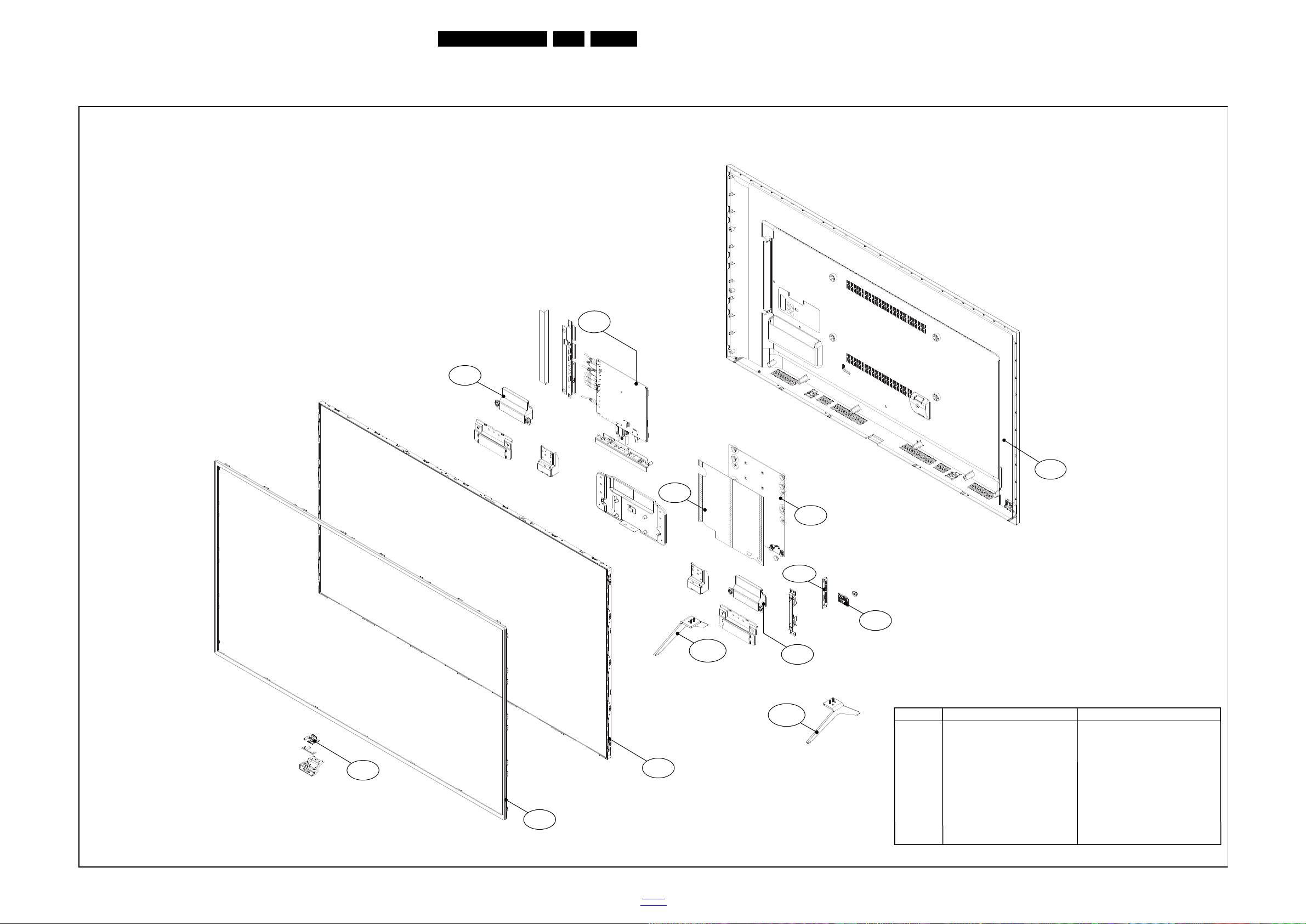
11. Styling Sheets
20160_800.eps
6601 series 50"
FOR ELECTRICAL PARTS/ASSEMBLIES SEE WIRING DIAGRAM CHAPTER 9
0030 Bezel
0040 Rear cover
0050R Stand_R
0050L Stand_L
0095 V0 SHEET
1050 Display panel
1053 Panel SSB
1054 Power Supply Unit
1056 IR/LED panel
1057 Keyboard control panel
1176 Remote control Not displayed
1184 Speakers
WiFi01 WiFi_USB
Pos No. Description Remarks
0040
0095
1050
1184
1057
1054
WIFI01
1056
0030
1053
0050R
0050L
1184
11.1 6601 series 50"
Styling Sheets
EN 69QM16.1L LA 11.
2016-Jul-08
back to
div.table
Page 70
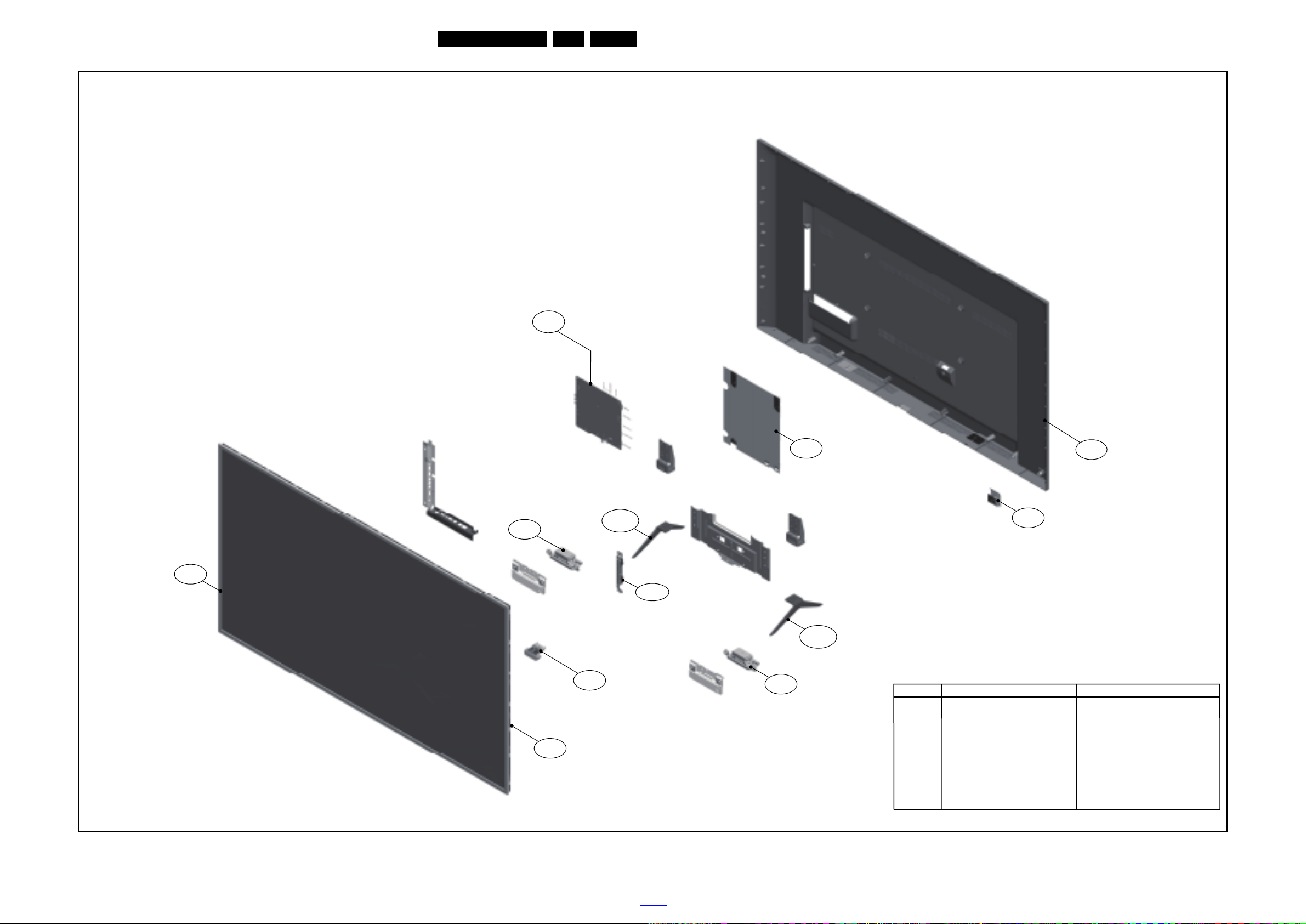
11.2 6601 series 55"
20160_801.eps
6601 series 55"
FOR ELECTRICAL PARTS/ASSEMBLIES SEE WIRING DIAGRAM CHAPTER 9
0030 Bezel
0040 Rear cover
0050R Stand_R
0050L Stand_L
1050 Display panel
1053 Panel SSB
1054 Power Supply Unit
1056 IR/LED panel
1057 Keyboard control panel
1176 Remote control Not displayed
1184 Speakers
WiFi01 WiFi_USB
Pos No. Description Remarks
0040
1050
1184
1057
1054
1184
WIFI01
1056
0030
1053
0050L
0050R
Styling Sheets
EN 70QM16.1L LA 11.
2016-Jul-08
back to
div.table
 Loading...