

Philips 42TA1800/93, 42TA2000/93, 37TA2000/93 Service Manual
Service
Service
Service
Service
Service
Service
Subject to modification Feb. 09 , 2006 EN: 3138 106 50050
Chassis: TPT1.0A LA
TFT WXGA LCD TV
Contents Page
1. Technical Specifications and Connections 2~4
2. Safety Instructions, Warnings and Notes 5
3. Directions for User 7
4. Mechanical Instructions 8~9
5. Wiring Diagram 10
Block Diagram 11~12
6. Circuits Diagrams & PWB Layouts
Chassis Overview & Exploded View 13~14
Diagram PWB
~6
PHILIPS
37TA1800/93
42TA1800/93
37TA2000/93
42TA2000/93
7. Alignments
Electrical Instructions&Serial NO.Definition 46~50
S
Circuit Descriptions and IC Data Sheets 53
Circuit Description 54
IC Data Sheets 55~60
Repair Flow Chart 61~62
9. Spare Parts List 63~73
10.42 Supplement Material
Diagram PWB
"
Power Board(42") (Diagram P)74 75 ~76
oftware Updrade With ISPWriter 51~52
8.
Contents Page
Contents
DSUB/DVI
HDMI
TUNNER
AV CONNECTOR
IO
CPU M30620SPGP
SVP-PX66-1
SVP-PX66-2
SVP-PX66-3
SVP-PX66-4
DDR 4Mx32
SOUND DELAY
AUDIO AMP
POWER 1
POWER2
RESET
(Diagram S-A01)15 33~34
(Diagram S-A02)16 33~34
(Diagram S-A03)17 33~34
(Diagram S-A04)18 33~34
(Diagram S-A05)19 33~34
(Diagram S-A06)20 33~34
(Diagram S-A07)21 33~34
(Diagram S-A08)22 33~34
(Diagram S-A09)23 33~34
(Diagram S-A10)24 33~34
(Diagram S-B11)25 33~34
(Diagram S-B12)26 33~34
(Diagram S-B13)27 33~34
AUDIO DECODER (Diagram S-B14)28 33~34
(Diagram S-B15)29 33~34
(Diagram S-B16)30 33~34
(Diagram S-B17)31 33~34
(Diagram S-B18)32 33~34
Power Board(37 (Diagram P)35 36~37
SIDE AV Board (Diagram A)38 39~40
IR Board (Diagram I)41 42~43
KEY Board (Diagram K)44 45
")
11.Different Parts List 78~84
Exploded View(42
")
77
12.Revision List 85
1. Technical Specifications and Connections
2
TPT1.0A LA
1. Technical Specifications and Connections
1.1 Technical Specifications
1.1.1Vision
:
3 Miscellaneous
Panel Model CLAA370WA03 (Supplier CPT)
Power supply:
AC-input : 90V ~ 264VAC,
50/60 2Hz
Power consumption : 170W/Max(at PC mode),170W/
Max(at TV mode) with Audio
Auto power saving : < 2W
Power cord length : 1.8M
Power cord type : European type and China type
Power indicator : LED (On: Blue ,Sleeping
mode: Amber )
(37")
T420XW01 (Supplier AUO)(42")
(37")
930.25(H) x 523.01(V) (42")
(37")
(42")
Pitch ( mm ) : 0.6(H) X 0.6(V)(37")
0.68(H) X 0.68(V)(42")
Color pixel arrangement : RGB vertical stripe
Display operating mode : Normally black
Color depth : 16.7M colors(8bits)
Brightness (cd/m^2) : 500(Center 1 points, Typ.)
Surface treatment : Hard coating(3H),
Electrical interface : LVDS
Outline Dimension(mm):877(H)X516.8(V)X55.5(D)(Typ.)(37")
983.0(H) x 576.0(V) x 54.2(D)(42")
Module weight (g) : 12,000(Typ.)
Backlight : 8 CCFL(37")
16 CCFL(42")
Horizontal scan : 30 ~ 63KHz
Vertical scan : 50 ~ 75 Hz
Sound systems : Stereo
Maximum power :2x10W(37")
(37")
Max(at TV mode) with Audio(42")
2 Sound
1.1.
Display type : LCD
Display area(mm) : 819.6(H) X 460.8(V)
Number of Pixels : 1366(H) x 768(V)
Contrast ratio : Typical 1200:1
Light output (cd/m2) : >400
Response time (ms) : Trg:8,Tfg:8 (Gray to Gray)
Viewing angle (HxV degrees): 170/170 (L/R,U/D) (CR >10)
178/178 (L/R,U/D) (CR >10)
1.1.
250W/Max(at PC mode),250W/
1.2.2 Input signal
1.2.2.1 Signal type
1.2.2.1.1PC mode signal type:
a.Analog Video: 15 pin D-sub ,0.7 Vp-p linear, positive
polarity&separate sync.( TTL level, positive
or negative polarity)
b.Audio signal : 3.5mm stereo mini-jack
Level: Nominal : 0.5 V rms.
- Maximum : 1.5 V rms.
-Impedance > 10 k .
c.Signal source: Pattern generator format as attachment table
1to12.
Reference generator: CHROMA 2200 or QuantumData 802R
O
O
Operating:
Temperature : 0 C to 40 C
Humidity : 10 to 90%(non condensing)
Altitude : 0 to 1,2000 feet
Air pressure : 645 mBAR
(guaranteed optical performance) : 5 to 35 C
(guaranteed functional performance) : 5 to 40 C
Index of this chapter:
1.1 Technical Specifications
1.2 Connections
Notes:
Some models in this chassis range have a different
mechanical construction. The information given here is
therefore model specific. At the moment of writing, not all
information was available (only the 37-inch TPT1.0A LA
model was available). As soon as the other models are
introduced, an update manual will be released.
Figures below can deviate slightly from the actual situation,
due to the different set executions.
Specifications are indicative (subject to change).
·
·
·
Storage
Temperature : -20 to 50 C
Humidity : 10 to 90% (non condensing )
Air pressure : 600 to 1100 mBAR ( non operating)
Note: recommend at 0 to 35 C, Humidity less than 60 %
Shipping
Temperature : -20 to 60 C
Humidity : 5 to 90% (non condensing )
Altitude : 0 to 40000 feet ( non operating )
Air pressure : 188 to 1100 ( non operating )
1.2 Connections
1.2.1Signal Connector(China model)
+
_
Fig1-1
Fig1-2
O
O
O
O
O
1
2
4
3
5
6
7
8
910
11
12
13
14
1516
1 ). Tuner: PAL D/K for China model
Multi-standard for WE model
2 ) SPDIF OUT : Digital audio output (HDMI audio output)
3 ). PVR OUT : Composite video output (CVBS) and audio
R/L(RCA jack)
4 ). AV audio IN : AV1 and S-Video audio R/L(RCAjack)
5 ). AV1 IN : Composite video input (AV1)
6 ). S-Video 1 IN : S-video input (S-Video 1)
7 ). Comp video 1 IN : HDTV input with YPbPr format with audio R/L.
8 ). Comp video 2 IN : HDTV input with YPbPr format with audio R/L.
9 ). PC audio IN: audio R/L(mini-jack).
10). PC IN: VGA input (D-SUB connectors)
11). HDMI : digital video and audio input
12). speaker output : external speakers output connectors
13). earphone : earphone jack
14). AV2 IN : Composite video input (AV2 side)
15). AV audio IN : AV2 and S-Video side audio R/L(RCA jack)
16). S-Video IN : S-video input (S-Video side)
3
TPT1.0A LA
1. Technical Specifications and Connections
1.2.2.1.2TV mode signal type
RF Signal : Aerial input / 10mV(30-100dBuV)
Video signal : CVBS input ( RCA jack) / 1Vpp (300mV-sync,
700mV-video.)
S video input / 1VppY-signal, +/-300mV C-signal
SCART input: CVBS
S SRGB signal ( for WE model only)
Comp video in(YPbPr input)/ 1Vpp Y signal, +/-350mV Pb,Pr signal
HDMI:Digital interface with 4 channels TMDS signal
CVBS output ( RCA jack) / 1Vpp (300mV-sync, 700mV-video.)
Audio signal : Audio (1) R/L for AV IN(AV and S-Video).
Level: - Nominal : 0.5 V rms.
- Maximum : 1.5 V rms.
- Impedance > 10 k
.
Audio (2) R/L for SCART IN
Level: - Nominal : 0.5 V rms.
- Maximum : 1.5 V rms.
- Impedance > 10 k
.
Audio (3) R/L for Comp video IN.
Level: - Nominal : 0.5 V rms.
-Maximum : 1.5 V rms.
- Impedance > 10 k
.
Audio (4) digital audio for HDMI Video IN.
1.2.2.1.3 PVR (CVBS) output:
Video: CVBS output 1Vpp / Impedance : 75
.
Audio: R/L output (from CVBS)
Level: - Nominal : 0.5 V rms.
- Maximum : 1.5 V rms.
- Impedance < 1 k
.
1.2.2.1.4 Scart output: ( for WE model only)
Video: CVBS output 1Vpp / Impedance : 75
.
Audio: R/L output (from CVBS)
Level: - Nominal : 0.5 V rms.
- Maximum : 1.5 V rms.
- Impedance < 1 k
.
1.2.2.1.5 SPDIF output: Serial digital audio output when input is HDMI.
1.2.2.1.6 Headphone
Audio: R/L output -10mW at 32
.
3.5mm stereo jack with switch
Impedance is between 8 and 600
.
1.2.2.2 TV system signal mode:
RF support:
China : PAL(D,K)
WE : PAL and SECAM(France).
CVBS/S-video: Support PAL, NTSC and SECAM colour system.
Comp video IN(YpbPr) : SDTV and HDTV, including 480i/p, 576i/p,
720p 50/60Hz, 1080i 50/60Hz.
HDMI IN : 480P, 576P ,720P/50Hz , 720P/60Hz , 1080i/50Hz ,
1080i/60Hz
PVR (CVBS out) : Support PAL, NTSC and SECAM colour system.
1.2.2.3 Sig nal cable
1.2.2.3.1 VGA s ign al cable
The input signals are applied to display through D-sub cable.
Length: 1.8 M +/- 50 mm (fixed)
Connector type: D-sub male.
With DDC_2B pin assignments.
Blue connector thumb-operated jackscrews
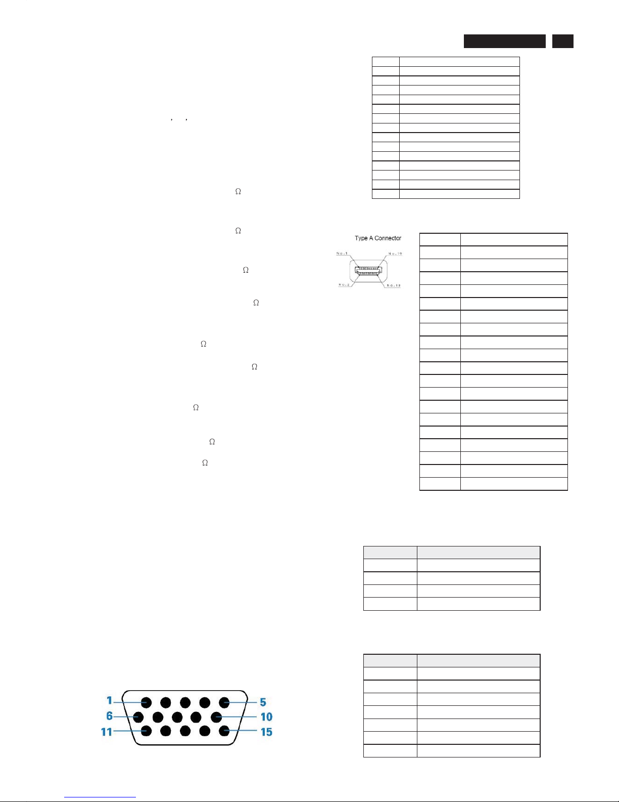
15-pin D-sub VGA connector of the signal cable:
1 Red video input
2 Green video input /SOG
3 Blue video input
4 GND
5 GND- cable detect
6 Red video ground
7 Green video ground
8 Blue video ground
9 DDC +3.3V (or 5V)
10 Logic ground
11 GND
12 Serial data line (SDA)
13 H. Sync / H+V
14 V. Sync
15 Data clock line (SCL)
1.2.2.3.2 HDMI for digital Video / Audio interface with pin assignment
as follows:
Pin No. Description
1RX2+
2GND
3RX2-
4RX1+
5GND
6RX1-
7RX0+
8GND
9RX0-
10 RXC+
11 GND
12 RXC-
13 CEC
14 NC
15 DDC clock
16 DDC data
17 GND
18 +5V POWER
19 Hot Plug Detect
1.2.2.3.3 CVBS
The input signals are applied to display through CVBS cable
Pin assignment
PIN NO. SIGNAL
1GND
2 CVBS
3 CVBS
4 CVBS
1.2.2.3.4 S-Video
The input signals are applied to display through S-Video cable
Pin assignment
PIN NO. SIGNAL
1GND
2GND
3GND
4GND
5GND
6LUMA
8 CHROMA
1. Technical Specifications and Connections
4
TPT1.0A LA
1.2.2.3.5 Component Video
The input signals are applied to display through Component
Video RCA Jack pin assignment
PIN NO. SIGNAL
1GND
2Redà Pr
3GND
4Blueà Pb
5GND
6GreenàY
1.2.2.3.6 SCART
Scart connector is only used in WE model. The Scart (Syndicat
des Constructeurs d'Appareils Radiorécepteurs et Televiseurs)
connector is used for combined audio and video connections.
Pin TV SCART
1 N/C
2 Right audio input
3 N/C
4 Audio ground
5 Blue ground
6 Left audio input
7 Blue output
8
0-2.5 volts (low) when:
TV output
4.5-7.5 volts (High -to-6v) wh en:
-inputting picture format setting is '16:9',
9-12 volts (hig h-to-12v) w hen:
-inputing picture format setting is '4:3'
9 Green ground
10 N/C
11 Green output
12 N/C
13 Red ground
14 N/C
15 Red output
16
0volt (low)when:-pin8oftheTVscartis
low
or when:
- Composite video signal
1-3 volts (hig h) when:
- video input setting is 'RGB',
17 Composite video output ground
18 Composite video input ground
19 N/C
20 Composite video input
21 Ground

5
TPT1.0A LA
2. Safety Instructions, Warnings and Notes
2.1 Safety Instructions
Safety regulations require that during a repair:
Connect the set to the AC Power via an isolation
transformer (> 800 VA).
Replace safety components, indicated by the symbol ,
only by components identical to the original ones. Any
other component substitution (other than original type) may
increase risk of fire or electrical shock hazard.
Safety regulations require that after a repair, the set must be
returned in its original condition. Pay in particular attention to
the following points:
Route the wire trees correctly and fix them with the
mounted cable clamps.
Check the insulation of the AC Power lead for external
damage.
Check the strain relief of the AC Power cord for proper
function.
Check the electrical DC resistance between the AC Power
plug and the secondary side (only for sets which have a AC
Power isolated power supply):
1. Unplug the AC Power cord and connect a wire
between the two pins of the AC Power plug.
2. Set the AC Power switch to the "on" position (keep the
AC Power cord unplugged!).
3. Measure the resistance value between the pins of the
AC Power plug and the metal shielding of the tuner or
the aerial connection on the set. The reading should be
between 4.5 Mohm and 12 Mohm.
4. Switch "off" the set, and remove the wire between the
two pins of the AC Power plug.
Check the cabinet for defects, to avoid touching of any
inner parts by the customer.
·
·
·
·
·
·
·
·
2. Safety Instructions, Warnings and Notes
index of this chapter:
2.1 Safety Instructions
2.2 Warnings
2.3 Notes
-6
-9
-12
the parts lists, are interchangeable per position with the
semiconductors in the unit, irrespective of the type
indication on these semiconductors.
Manufactured under license from Dolby Laboratories.
"Dolby" and the "double-D symbol", are trademarks of
Dolby Laboratories.
All resistor values are in ohms and the value multiplier is
often used to indicate the decimal point location (e.g. 2K2
indicates 2.2 kohm).
Resistor values with no multiplier may be indicated with
either an "E" or an "R" (e.g. 220E or 220R indicates 220
ohm).
All capacitor values are given in micro-farads (u= x10 ),
nano-farads (n= x10 ), or pico-farads (p= x10 ).
Capacitor values may also use the value multiplier as the
decimal point indication (e.g. 2p2 indicates 2.2 pF).
An "asterisk" (*) indicates component usage varies. Refer
to the diversity tables for the correct values.
The correct component values are listed in the Electrical
Replacement Parts List. Therefore, always check this list
when there is any doubt.
General
Although (LF)BGA assembly yields are very high, there may still be
a requirement for component rework. By rework, we mean the
process of removing the component from the PWB and replacing it
with a new component. If an (LF)BGA is removed from a PWB, the
solder balls of the component are deformed drastically so the
removed (LF)BGA has to be discarded.
Device Removal
As is the case with any component that, it is essential when
removing an (LF)BGA, the board, tracks, solder lands, or
surrounding components are not damaged. To remove an(LF)BGA,
the board must be uniformly heated to a temperature close to the
reflow soldering temperature. A uniform temperature reduces the
chance of warping the PWB.To do this, we recommend that the
board is heated until it is certain that all the joints are molten.
Then carefully pull the component off the board with a vacuum
nozzle. For the appropriate temperature profiles, see the IC data
sheet.
Area Preparation
When the component has been removed, the vacant IC area must
be cleaned before replacing the (LF)BGA.Removing an IC often
leaves varying amounts of solder on the mounting lands. This
excessive solder can be removed with either a solder sucker or
solder wick. The remaining flux can be removed with a brush and
cleaning agent.After the board is properly cleaned and inspected,
apply flux on the solder lands and on the connection balls of
the (LF)BGA.
Note: Do not apply solder paste, as this has shown to result in
problems during re-soldering.
Device Replacement
The last step in the repair process is to solder the new component
on the board. Ideally, the (LF)BGAshould be aligned under a
microscope or magnifying glass. If this is not possible, try to align
the (LF)BGA with any board markers. To reflow the solder, apply a
temperature profile according to the IC data sheet. So as not to
damage neighbouring components, it may be necessary to reduce
some temperatures and times.
More Information
For more information on how to handle BGA devices, visit this
URL: (needs subscription,
not available for all regions). After login, "select Magazine", then
go to "Workshop Information". Here you will find Information on
how to deal with BGA-ICs.
2.3.2 Schematic Notes
2.3.3 Rework on BGA (Ball Grid Array) Ics
www.atyourservice.ce.philips.com
2.3 Notes
2.3.1 General
Measure the voltages and waveforms with regard to the
chassis (= tuner) ground ( ), or hot ground ( ), depending
on the tested area of circuitry. The voltages and waveforms
shown in the diagrams are indicative. Measure them in the
Service Default Mode (see chapter 5) with a color bar
signal and stereo sound (L: 3 kHz, R: 1 kHz unless stated
otherwise) and picture carrier at 475.25 MHz for PAL, or
61.25 MHz for NTSC (channel 3).
Where necessary, measure the waveforms and voltages
with ( ) and without ( ) aerial signal. Measure the
voltages in the power supply section both in normal
operation ( ) and in stand-by ( ). These values are
indicated by means of the appropriate symbols.
The semiconductors indicated in the circuit diagram and in
··
··
··
2.2 Warnings
All ICs and many other semiconductors are susceptible to
electrostatic discharges (ESD ). Careless handling
during repair can reduce life drastically. Make sure that,
during repair, you are connected with the same potential as
the mass of the set by a wristband with resistance. Keep
components and tools also at this same potential.
Be careful during measurements in the high voltage
section.
Never replace modules or other components while the unit
is switched "on".
When you align the set, use plastic rather than metal tools.
This will prevent any short circuits and the danger of a
circuit becoming unstable.
·
·
·
·
·
·
·
·
·
·
·
6
TPT1.0A LA
2. Safety Instructions, Warnings and Notes
This sign normally has a diameter of 6 mm, but if there is less
space on a board also 3 mm is possible.
In case of doubt wether the board is lead-free or not (or with
mixed technologies), you can use the following method:
Always use the highest temperature to solder, when using
SAC305 (see also instructions below).
De-solder thoroughly (clean solder joints to avoid mix of
two alloys).
: For BGA-ICs, you must use the correct temperatureprofile,
which is coupled to the 12NC. For an overview of these
profiles, visit the website
(needs subscription, but is not available for all regions)
You will find this and more technical information within the
"Magazine", chapter "Workshop information".
For additional questions please contact your local repairhelpdesk.
Caution
Due to lead-free technology some rules have to be respected
by the workshop during a repair:
Use only lead-free soldering tin . If lead-free solder paste
is required,please contact the manufacturer of your soldering
equipment. In general, use of solder paste within
workshops should be avoided because paste is not easy to
store and to handle.
Use only adequate solder tools applicable for lead-free
soldering tin. The solder tool must be able
-To reach at least a solder-tip temperature of 400 C.
-To stabilise the adjusted temperature at the solder-tip.
-To exchange solder-tips for different applications.
Adjust your solder tool so that a temperature around 360 C
- 380 C is reached and stabilised at the solder joint.
Heating time of the solder-joint should not exceed~4sec.
Avoid temperatures above 400 C, otherwise wear-out of
tips will rise drastically and flux-fluid will be destroyed. To
avoid wear-out of tips, switch "off" unused equipment or
reduce heat.
Mix of lead-free soldering tin/parts with leaded soldering
tin/parts is possible but PHILIPS recommends strongly to
avoid mixed regimes. If not to avoid, clean carefully the
solder-joint from old tin and re-solder with new tin.
Use only original spare-parts listed in the Service-Manuals.
Not listed standard material (commodities) has to be
purchased at external companies.
Special information for lead-free BGAICs: these ICs will be
delivered in so-called "dry-packaging" to protect the IC
against moisture. This packaging may only be opened
short before it is used (soldered). Otherwise the body of the
IC gets "wet" inside and during the heating time the
structure of the IC will be destroyed due to high (steam-)
pressure inside the body. If the packaging was opened
before usage, the IC has to be heated up for some hours
(around 90C)fordrying (think of ESD-protection !).
For sets produced before 1.1.2005, containing leaded
soldering tin and components, all needed spare parts will
be available till the end of the service period. For the repair
of such sets nothing changes.
Do not re-use BGAs at all!
www.atyourservice.ce.philips.com
Fig 2-1 Lead-free logo
2.3.4 Lead Free Solder
Philips CE is going to produce lead-free sets (PBF) from
1.1.2005 onwards.
Lead-free sets will be indicated by the PHILIPS-lead-free logo
on the Printed Wiring Boards (PWB):
In case of doubt whether the board is lead-free or not (or with
mixed technologies), you can use the following method:
Always use the highest temperature to solder, when using
SAC305 (see also instructions below).
De-solder thoroughly (clean solder joints to avoid mix of
two alloys).
: For BGA-ICs, you use the correct temperatureprofile,
which is coupled to the 12NC. For an overview of these
profiles, visit the website
(needs subscription, but is not available for all regions)
You will find this and more technical information within the
"Magazine", chapter "Workshop information".
For additional questions please contact your local repair help
desk.
Caution must
www.atyourservice.ce.philips.com
While some sources are expected to have a possible
dangerous impact, others of quite high potential are of
limited current and are sometimes held in less regard.
While some may not be
dangerous in themselves, they can cause unexpected
reactions - reactions that are best avoided. Before reaching
into a powered TV set, it is best to test the high voltage
insulation. It is easy to do, and is a good service precaution.
2.3.5 Practical Service Precautions
It makes sense to avoid exposure to electrical shock.
Always respect voltages.
·
·
·
·
·
·
·
·
·
·
·
·
·

7
TPT1.0A LA
3. Directions for Use
3. Directions for Use
You can download this information from the following websites:
http://www.philips.com/support
http://www.p4c.philips.com
8
TPT1.0A LA
4. Mechanical Instructions
Front view
Back view
Step 1. Remove the stand and speaker.
a. Remove the 2 screws to remove the stand as Fig.3
Fig.3
Fig.2
Fig.1
Step 2. Remove the Back cover as Fig.5.
a.
Remove the 20 screws to remove the Back cover as Fig.5
Fig.6
Fig.7
Fig.8
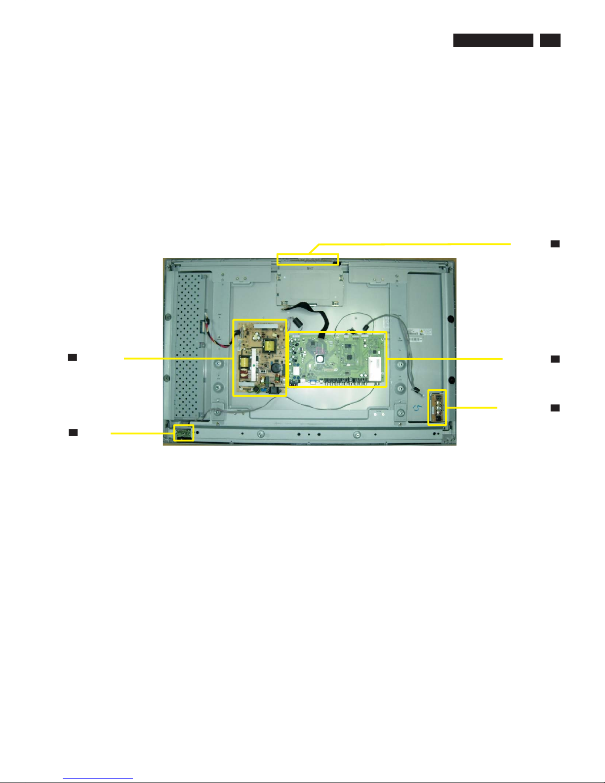
Step 4. Remove the Scaler and Power board.
a. Remove the 11 screws as Fig. 9
b. Remove the 12 screws to remove the Scaler and Power board as
Fig10~11
Fig.9
Fig. 10
Fig.4
Fig.5
4. Mechanical Instructions
Index of this chapter:
4.1 Assy/Panel Removal
4.2 Set Re-assembly
4.1 Assy/Panel Removal
b. Remove the 4 screws and 2 cables to remove the speaker as Fig.4
Step 3. Remove IR, Side AV, Key board and Main shield assy as Fig.6~8.
a. Remove the 4 screws to remove the as Fig.6
b. Remove the 1 cable and 2 screws to remove Side AV board as Fig.7
c. Remove the 1 cable and 2 screws to remove IR board as Fig.7
d. Remove the 1 cable to remove Key board as Fig.7
e. Remove the the other 2 cables and 6 screws to remove the Main
shield assy as Fig.7~8
9
TPT1.0A LA
4. Mechanical Instructions
Step 5. Remove the Bezel assy as Fig.12~Fig.15 .
Remove the 5 screws
Remove the Bezel assy
a. as Fig.12
b. Remove the 4 screws as Fig.13
c. Remove the 4 screws as Fig.14
d . as Fig.15
In warranty, it is not allowed to disassembly the LCD panel, even the
backlight unit defect.
Out of warranty, the replacment of backlight unit is a correct way
when the defect is cused by backlight (CCFL,Lamp).
Fig. 14
Fig. 15
Fig. 13
4.2 Set Re-assembly
To re-assemble the whole set, execute all processes in reverse
order.
Notes:
a. While re-assembling, make sure that all cables are placed
and connected in their original position.
b. Pay special attention not to damage the EMC foams at the
SSB shielding. Check that EMC foams are put correctly on
their places.
Fig. 11
Fig. 12
10
TPT1.0A LA
5. Block Diagram
5. Block Diagram
Index of this chapter:
5.1
5.2 Block Diagram
Wiring Diagram
5.1 Wiring Diagram
1921 2P1921
2P
COMPONENT
19076P1907
6P
COMPONENTSIDE
16308P1630
8P
1
8
CN109
10PIN
CN109
10PIN
CN114
6PIN
CN114
6PIN
CN113
2PIN
CN113
2PIN
CN117
10PIN
CN117
10PIN
COMPONENT SIDE
1089 10P1089 10P
1071
1063 12P1063 12P
1088 12P1088 12P
1064
CN112
3PIN
CN112
3PIN
3138 14723781
PHILIPS
3138 14723781
PHILIPS
1
12
1
12
1
10
1
10
1
2
1
6
10
1
1
6
1
3
1
2
11
TPT1.0A LA
M24C02
M30620SPGP
IS61LV256-12T
SRAM
for TT
(NI)
24LC64
SST39VF088
FLASH
74LV4053PW
M24C02
74LVC14ADT
FQ1256
SVP-PX66
CS4344
K4D263238G-VC33
DDR
(2.5V)
5V_SCL
5V_SDA
SIF_OUT
TV_CVBS
ISP_SW
TX
RX
SCL
SDA
VGA_HSIN
VGA_VSIN
PC_HSIN
PC_VSIN
A0-A19
AD0-AD7
CPU_RESET
RY_BY
8051_WR#
8051_RD#
CE#
A0-A14
SRAM_ENABLE
SCLE
SDAE
E_PAGE
DDCSCL
DDCSDA
AD0-AD7
8051_WR#
8051_RD#
PX_MD0-31
PX_DQS0-3
PX_MA0-11
PX_BA0-1
PX_RAS#/CAS#
PX_CS0#
PX_WE#
PX_CLKE
PX_MCK0/0#
PC_R/G/BIN
YPbPr1_Y/Pb/Pr
YPbPr2_Y/Pb/Pr
CVBS1_MP
CVBS2_MP
SV1_Y/C_MP
SV2_Y/C_MP
PC_VSIN
PC_HSIN
74HC4052D
MSP3410G
TDA1308T
TPA3008D2
HDMI R/L
DSUB R/L
COMP1 R/L
COMP2 R/L
SC3_IN_L
SC3_IN_R
CVBS1 R/L
CVBS2 R/L
SIF_OUT
HP_R_OUT
HP_L_OUT
HP_ROUT
HP_LOUT
AR_DACM
AL_DACM
ROUT+/-
LOUT+/-
MSP_INT
5V_SDA
5V_SCL
PX_INT#
HDMI_HOTPLUG
DETECT_VGA
PANEL_PWR
INVERTER_ON_OFF
SOUND_EN
SB_PWR
POWER_ON
KEYA
HP_DET
3V_SCL
3V_SDA
8051_ALE
8051_WR#
8051_RD#
HDMI_SD0
HDMI_SCK
HDMI_WS
HDMI_MCLK
+5V
3.3V_SB
3.3V_SB
3.3V_SB
PX_VDDMQ
PX_VD33
PX_VA18
PX_VL18
PX_HMMI33
PX_VDDMQ
PX_VDDM
5V_SB
DDC_5V
DDC_5V
3.3V_SB
+5V
+5V
+5V
+16V
+5V
BRIGHT_ADJ
DDC_WP
8051_CS2PX
REMOTE_3V
CPU_RESET
8051_A0-7
8051_AD0-7
RESET_H
PCA9512
3V_SCL
3V_SDA
3.3V_SB
5V_SB
HDMI
Connector
RX5V1_DD
C_SDA
RX5V1_DD
C_SCL
HDMI1_RX0/
1/2/3/C+-
HDMI1_RX0/
1/2/3/C+-
DSUB
Connector
PC_R/G/BIN
SW4
SW3
SW4
SW3
PX_VD18
HDMI_SPDIF
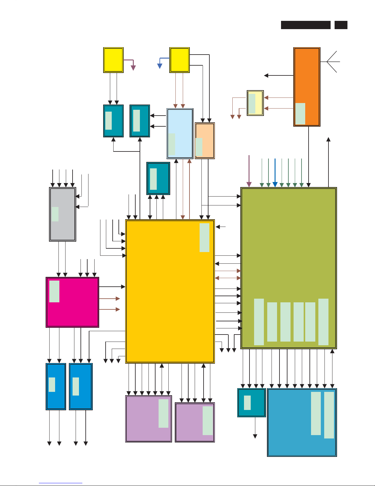
Function block of scaler Board
5.2 Block Diagram
5. Block Diagram
12
TPT1.0A LA
5. Block Diagram
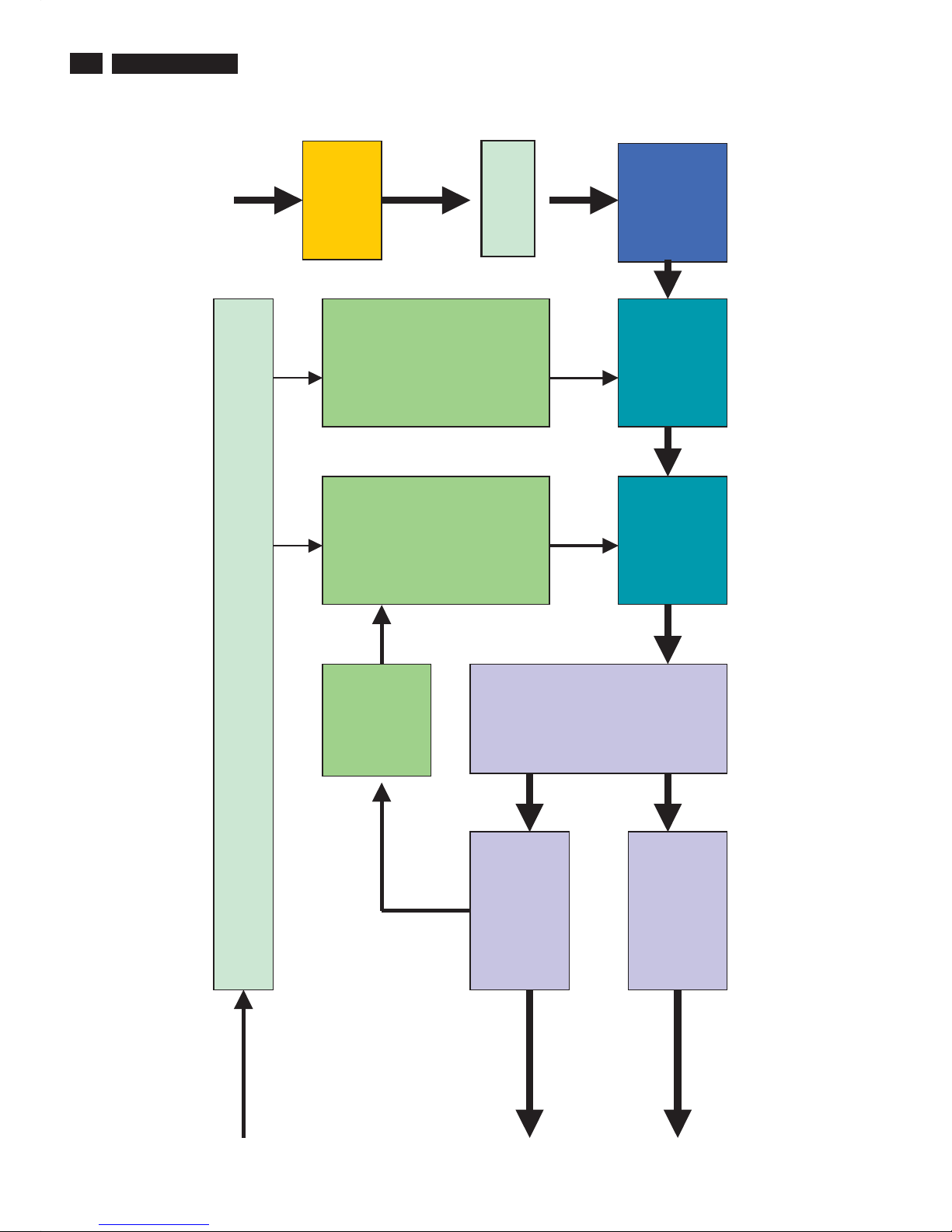
Function block of power Board
Transformer
EQ40
Photo-coupler
TCET1103(G)
Protect /
Feedback
network
PWM control
TEA1507P &
STW18NK80Z
AC Inlet
AC to DC
KBU8J
AC to DC
STPS40H100CW
24V 9A_42”
24V 7A_37”
Inverter board
16V 2.5A
Panel/scalar/
Audio
AC Input
90 ~ 264V
EMI
FILTER
AC to DC
MBRF10H100CT
PFC control
L6562 &
STW26NM60
Control interface
Control from
scalerboard
Photo-coupler
TCET1103(G)
13
TPT1.0A LA
Index of this chapter:
6.1 Chassis Overview
6.2 Exploded View
6.3 Scaler Board Schematic Diagram & Layouts
6.4 Power Board Schematic Diagram & Layouts
6.5 SIDE AV Schematic Diagram & Layouts
6.6 IR Schematic Diagram & Layouts
6.7 KEY Schematic Diagram & Layouts
Board
Board
Board
6.1 Chassi Overview
I
IR Board
Power Board
P
Scaler Board
S
Side AV Board
A
Key Board
K
6.Circuit Diagram & PWB Layouts
14
TPT1.0A LA
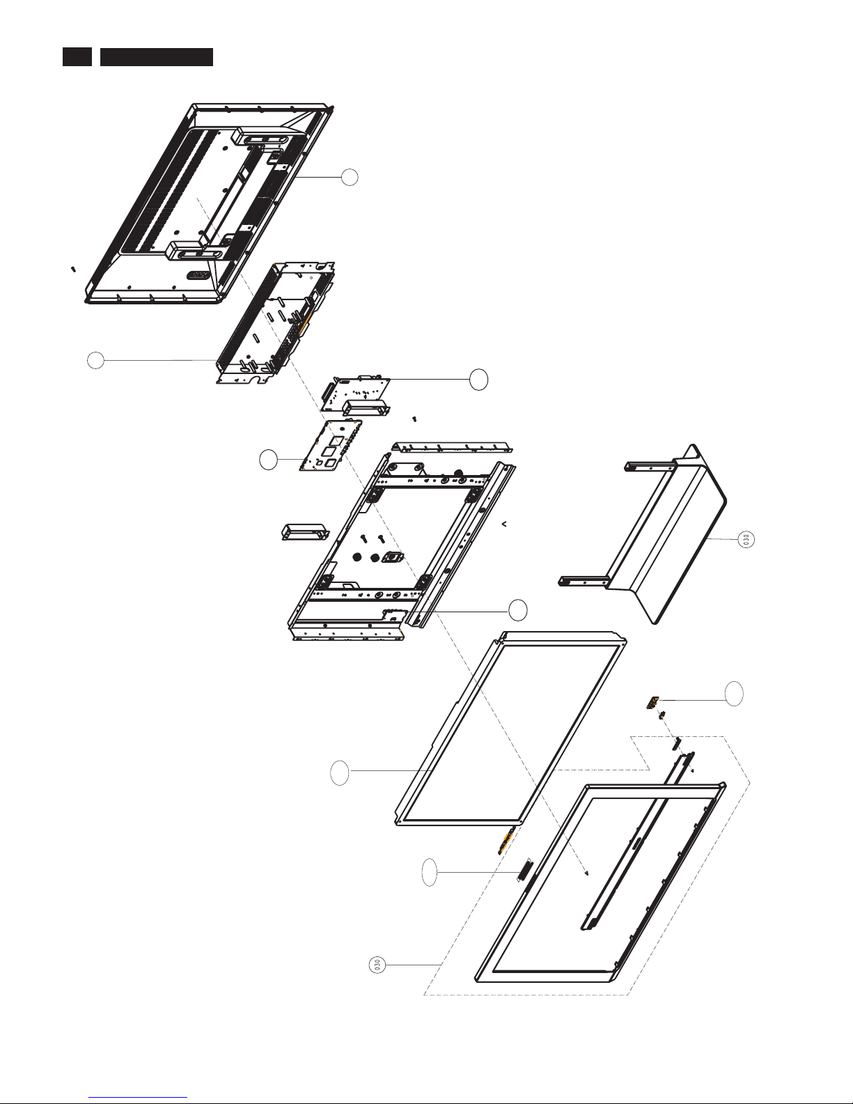
6.2 37 Exploded View"
313815761291
BACK COVER ASSY
40
313815761281
MAIN SHIELD ASSY
1057
996500039544
KEY BOARD
996500039543
IR ASSY
1056
823827720921
CPT CLAA370WA03
1050
313815761441
FRONT BEZEL ASSY
6.Circuit Diagram & PWB Layouts
313815761451
BASE ASSY
090
1054
313815864961
POWER PCB ASSY
1053
996500039547
SCALER BOARD_VISION-D
1055
96500039542
SIDE_AV_BOARD_VISION_D
6.3.1 Scaler Schematic Diagram-ContentsBoard
15
TPT1.0A LA
6.Circuit Diagrams and PWB Layouts
S-01
6.3.2 Scaler Schematic Diagram - DSUB/DVIBoard
16
TPT1.0A LA
6. Circuit Diagrams and PWB Layouts
S-02
6.3.3 Scaler Schematic Diagram - HDMIBoard
17
TPT1.0A LA
6.Circuit Diagrams and PWB Layouts
S-03
6.3.4 Scaler Schematic Diagram - TUNNERBoard
18
TPT1.0A LA
6. Circuit Diagrams and PWB Layouts
S-04
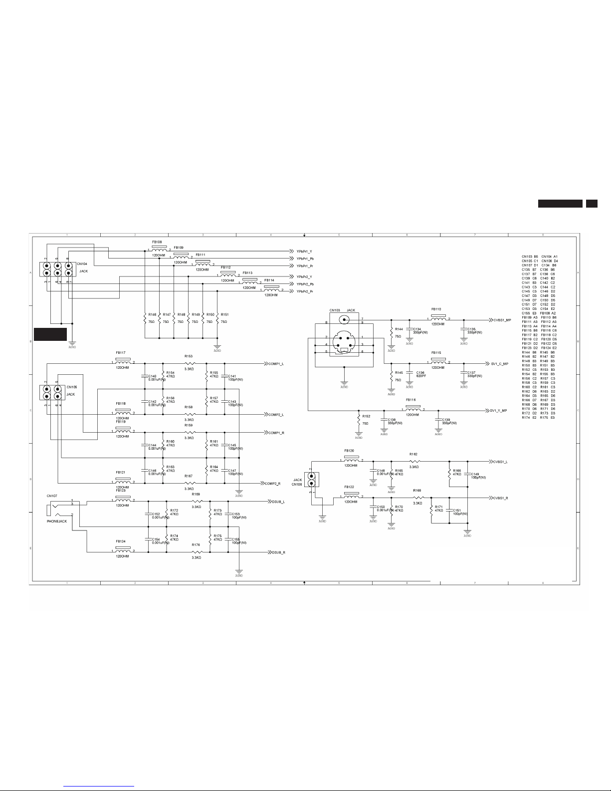
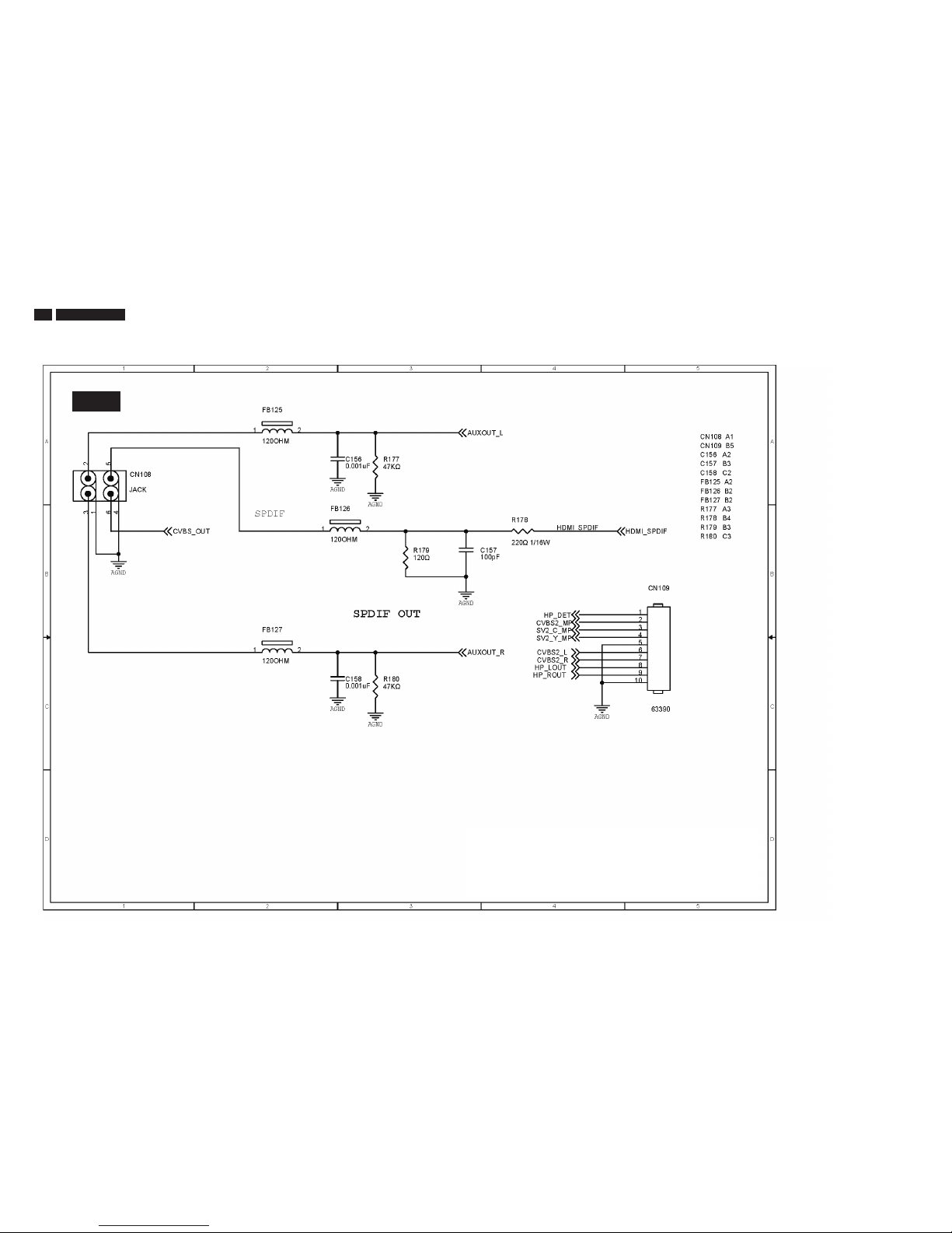
6.3.5 Scaler Schematic Diagram - AV CONNECTORBoard
19
TPT1.0A LA
6.Circuit Diagrams and PWB Layouts
S-05
6.3.6 Scaler Schematic Diagram - IOBoard
20
TPT1.0A LA
6. Circuit Diagrams and PWB Layouts
S-06
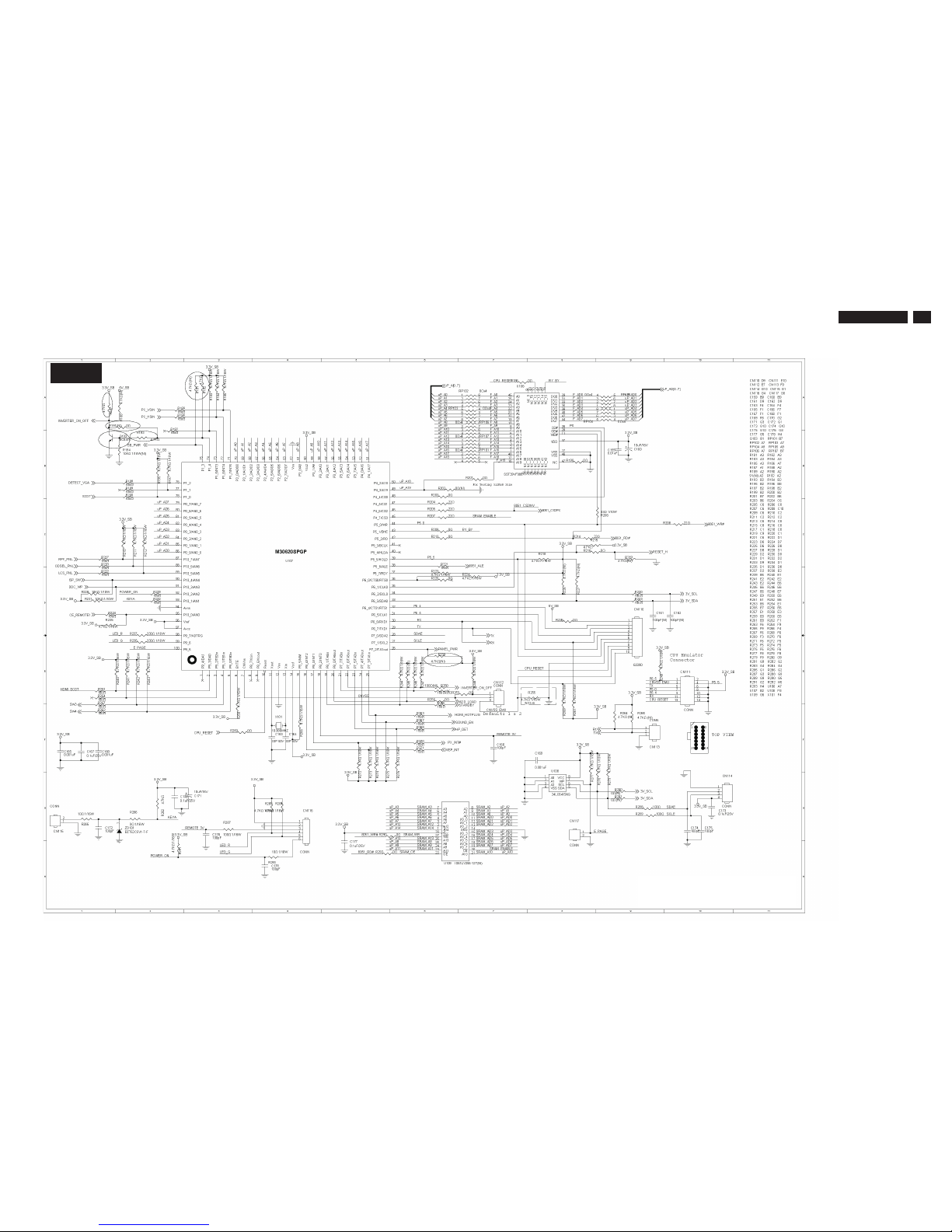
6.3.7 Scaler Schematic Diagram - CPU M30620SPGPBoard
21
TPT1.0A LA
6.Circuit Diagrams and PWB Layouts
S-07
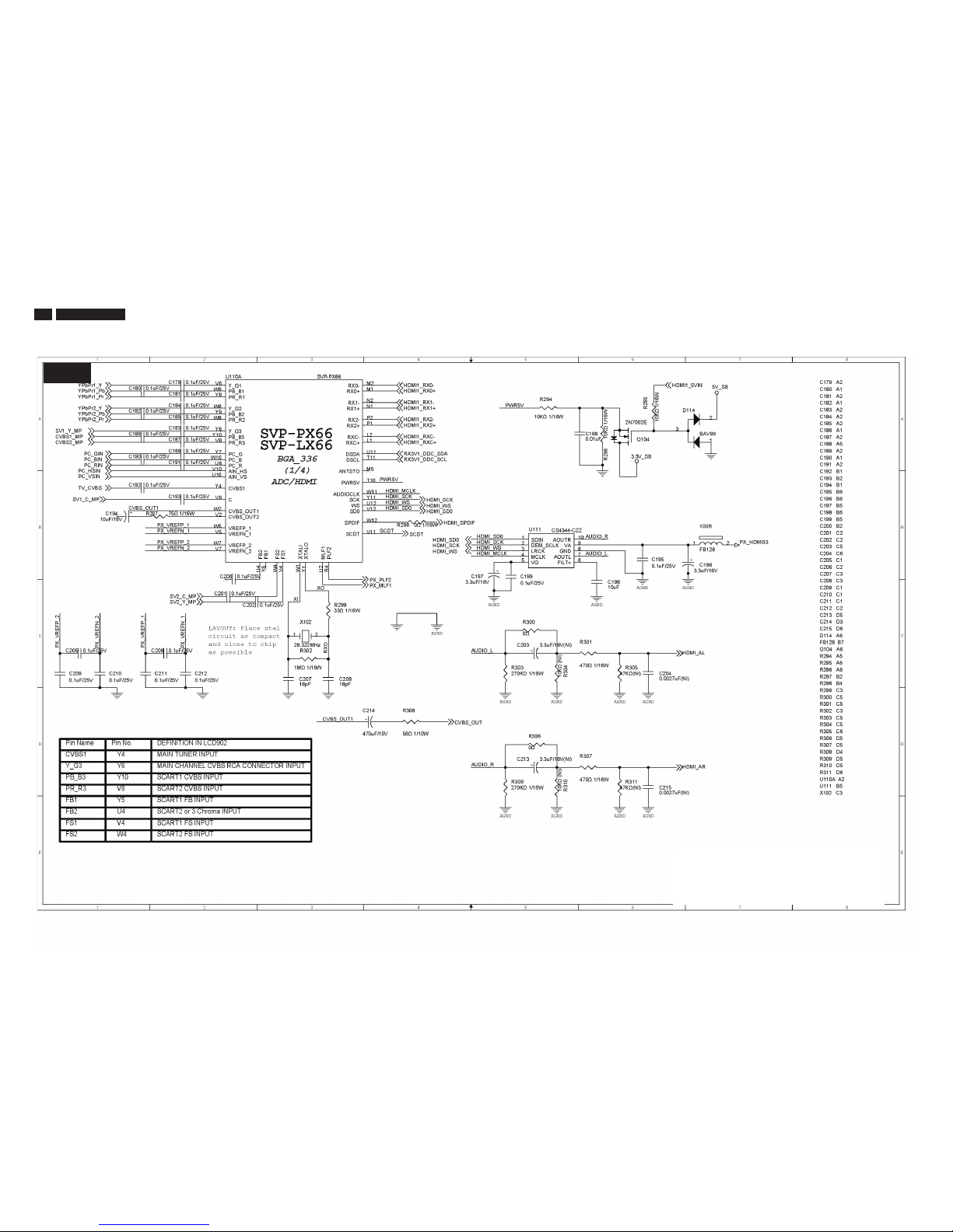
6.3.8 Scaler Schematic Diagram - SVP-PX66-1Board
22
TPT1.0A LA
6. Circuit Diagrams and PWB Layouts
S-08
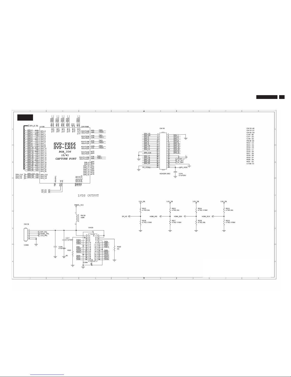
6.3.9 Scaler Schematic Diagram - SVP-PX66-2Board
23
TPT1.0A LA
6.Circuit Diagrams and PWB Layouts
S-09
24
TPT1.0A LA
6. Circuit Diagrams and PWB Layouts
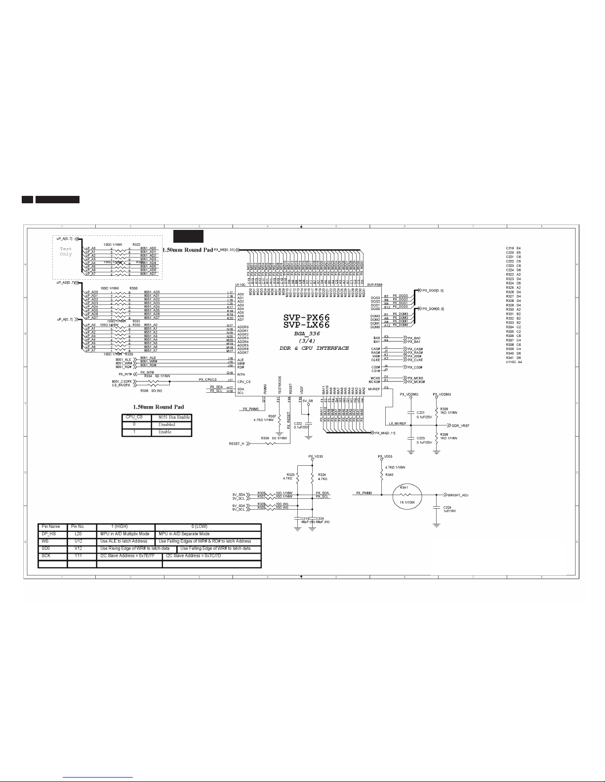
6.3.10 Scaler Schematic Diagram - SVP-PX66-3Board
S-10
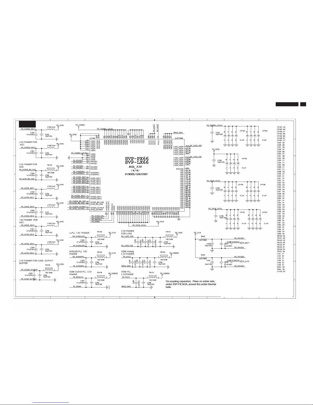
6.3.11 Scaler Schematic Diagram - SVP-PX66-4Board
25
TPT1.0A LA
6.Circuit Diagrams and PWB Layouts
S-11

6.3.12 Scaler Schematic Diagram - DDR 4Mx32Board
26
TPT1.0A LA
6. Circuit Diagrams and PWB Layouts
S-12
 Loading...