

Philips 26PFL3404D, 42PFL3604D Schematic
Colour Television Chassis
18291_000_090609.eps
090609
TPM2.1E
LA
Contents Page Contents Page
1. Revision List 2
2. Technical Specifications, Connections 2
3. Precautions, Notes, and Abbreviation List 7
4. Mechanical Instructions 11
5. Service Modes, Error Codes, and Fault Finding 18
6. Alignments 21
7. Circuit Descriptions 24
8. IC Data Sheets 32
9. Block Diagrams
Wiring Diagram Click 19/22" 49
Wiring Diagram 22PFL5604D/12 50
Wiring Diagram 26/32" 51
Wiring Diagram 42" 52
Block Diagram Click 19/22" 53
Block Diagram 26/32/42" 54
I2C Overview 19/22" 55
I2C Overview 26/32/42" 56
10. Circuit Diagrams and PWB Layouts DrawingPWB
Power board: Adapter, Click 19/22"
Power Board: Inverter, Click 19/22" (A02) 58 59-60
Power Board: Adapter, 22PFL5604D/12 (A01) 61 63-63
Power Board: Inverter, 22PFL5604D/12 (A02) 62 63-63
Power board: Adapter, 26/32" (LGD) (A01) 64 66-67
Power board: Inverter, 26/32" (LGD) (A02) 65 66-67
Power board: Adapter, 26/32" (AUO) (A01) 68 69-70
Power board: Adapter, 37/42" (A01) 71 73-74
Power board: Inverter, 37/42" (A02) 72 73-74
SSB 19/22": DC-DC (B01) 75 89-98
SSB 19/22": DC-DC (B02) 76 89-98
SSB 19/22": Tuner (B03) 77 89-98
SSB 19/22": MT5362 Bypass/Trap. (B04) 78 89-98
SSB 19/22": MT5362 Peripheral/USB2.0 (B05) 79 89-98
SSB 19/22": DDR2 Memory (B06) 80 89-98
SSB 19/22": Flash, J-TAG, Uart, IR (B07) 81 89-98
©
Copyright 2010 Koninklijke Philips Electronics N.V.
All rights reserved. No part of this publication may be reproduced, stored in a
retrieval system or transmitted, in any form or by any means, electronic, mechanical,
photocopying, or otherwise without the prior permission of Philips.
(A01) 57 59-60
SSB 19/22": MT8295/CI card (B08) 82 89-98
SSB 19/22": Scart1/Monitor out (B09) 83 89-98
SSB 19/22": YPbPr/VGA input (B10) 84 89-98
SSB 19/22": Side AV/SP-DIF/DVD (B11) 85 89-98
SSB 19/22": HDMI/Side HDMI input (B12) 86 89-98
SSB 19/22": Audio amp/HP out (B13) 87 89-98
SSB 19/22": LVDS output (B14) 88 89-98
SSB 26/32/42": DC-DC (B01) 99 113-122
SSB 26/32/42": DC-DC (B02) 100 113-122
SSB 26/32/42": Tuner (B03) 101 113-122
SSB 26/32/42": MT5362 Bypass/Trap (B04) 102 113-122
SSB 26/32/42": MT5362 Peripheral/USB (B05) 103 113-122
SSB 26/32/42": DDR2 Memory (B06) 104 113-122
SSB 26/32/42": Flash, J-TAG, Uart, IR (B07) 105 113-122
SSB 26/32/42": MT8295/CI card (B08) 106 113-122
SSB 26/32/42": Scart1/Scart2 (B09) 107 113-122
SSB 26/32/42": YPbPr/VGA input (B10) 108 113-122
SSB 26/32/42": Side AV/SP-DIF output (B11) 109 113-122
SSB 26/32/42": HDMI inputs (B12) 110 113-122
SSB 26/32/42": Audio amp/HP out (B13) 111 113-122
SSB 26/32/42": LVDS output (B14) 112 113-122
IR Board Click (J) 123 124
IR Board P&S (J) 125 126
Keyboard Control Panel (E) 127 128
Published by QiM/JY 1061 BU TV Consumer Care, the Netherlands Subject to modification EN 3122 785 18293
2010-Jun-18
EN 2 TPM2.1E LA1.
1. Revision List
Revision List
Manual xxxx xxx xxxx.0
• First release.
Manual xxxx xxx xxxx.1
• Updated the SAM and CSM content of chapter 5.
• Chapter 2: Added connection overview diagram (P&S
styling).
• Chapter 4: Added cable dressing diagram and updated the
processes of the removal styling.
– Added cable dressing for 32PFL3404D/12.
– Added cable dressing for 42PFL3604D/12 AUO panel.
• Chapter 7: Added SSB top view diagram
• Chapter 8: Added MT5632ANG -B IC SPEC.
• Chapter 9: Added and updated wiring diagram and block
diagram.
• Chapter 10: Added power board and IR board circuit
diagrams and PWB Layouts.
Manual xxxx xxx xxxx.2
• Added 22HFL3331D/10 set to the manual.
• Chapter 2: Updated connection overview diagram.
• Chapter 5: Updated the content of the chapter 5.
• Chapter 7: Updated SSB cell layout.
• Chapter 9: Updated wiring diagram and block diagram.
Manual xxxx xxx xxxx.3
• Added 19HFL3331D/10 set to the manual.
• Added 22HFL4371D/10 set to the manual.
• Added 26HFL3331D/10 set to the manual.
• Added 26HFL4371D/10 set to the manual.
• Added 26PFL3404D/05 set to the manual.
• Added 32HFL4351D/10 set to the manual.
• Chapter 2: Updated connection overview information.
• Chapter 5: Updated/added display codes.
• Chapter 7: Updated Power Diagrams.
2. Technical Specifications, Connections
Index of this chapter:
2.1
Technical Specifications
2.2 Directions for Use
2.3 Connections
2.4 Chassis Overview
Notes:
• Figures can deviate due to the different set executions.
• Specifications are indicative (subject to change).
2.2 Directions for Use
Directions for use can be downloaded from the following
websites:
http://www.philips.com/support
http://www.p4c.philips.com
2.1 Technical Specifications
For on-line product support please use the links in. Here is
product information available, as well as getting started, user
manuals, frequently asked questions and software & drivers.
Table 2-1 Described Model Numbers
Model Number Styling Published in
19PFL3404D/12
19PFL3404H/12
22PFL3404D/12
22PFL3404H/12
26PFL3404D/12
26PFL3404H/12
32PFL3404D/12
42PFL3604D/12
19PFL3404D/05
22PFL3404D/05
26PFL3404D/05
26HFL3331D/10
32PFL3404H/12
42PFL3604H/12
22PFL5604D/12 P&S
22HFL3331D/10
22HFL4371D/10
26HFL4371D/10
32HFL4351D/10
19HFL3331D/10 3122 785 18293
Click
Click
3122 785 18290
3122 785 18291
3122 785 18292
Note: The given Model Numbers are subject to change.
2010-Jun-18
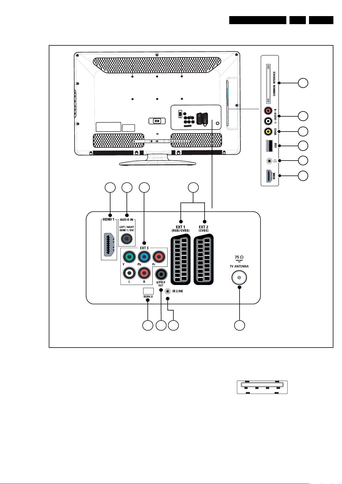
2.3 Connections
18290_001_090324.eps
100104
13
12
11
10
14
6
8
9
4
16
1
2
3
17
*
Note:
Connectors marked with a “*” are optional.
*
Technical Specifications, Connections
EN 3TPM2.1E LA 2.
Figure 2-1 Connection overview Click 19" and 22"
2010-Jun-18
EN 4 TPM2.1E LA2.
4
16
5
18291_001_090609.eps
100104
13
12
11
10
1
2
14
3
15
6
8
9
Technical Specifications, Connections
2010-Jun-18
Figure 2-2 Connection overview 22PFL5604D/12
Technical Specifications, Connections
4
5
16
Note:
Connectors marked with a “*” are optional.
18290_002_090330.eps
090415
12
11 1 7
10
1
2
67
3
8
9
*
*
1 2 3 4
10000_022_090121.eps
090121
EN 5TPM2.1E LA 2.
Note: The following connector colour abbreviations are used
(acc. to DIN/IEC 757): Bk= Black, Bu= Blue, Gn= Green,
Gy= Grey, Rd= Red, Wh= White, Ye= Yellow.
Figure 2-3 Connection overview 26", 32" and 42"
4 - USB2.0
2.3.1 Side Connections
1 - Common Interface
68p -See diagram B08 jk
2 - Cinch: Audio - In
Rd - Audio R 0.5 V
Wh - Audio L 0.5 V
3 - Cinch: Video CVBS - In, Audio - In
Ye - Video CVBS 1 V
/ 10 kΩ jq
RMS
/ 10 kΩ jq
RMS
/ 75 Ω jq
PP
Figure 2-4 USB (type A)
1-+5V k
2 - Data (-) jk
3 - Data (+) jk
4 - Ground Gnd H
2010-Jun-18
EN 6 TPM2.1E LA2.
10000_017_090121.eps
090428
19
1
18 2
21
20
1
2
10000_001_090121.eps
090121
1
6
10
11
5
15
10000_002_090121.eps
090127
Technical Specifications, Connections
5 - HDMI: Digital Video, Digital Audio - In
Figure 2-5 HDMI (type A) connector
1 - D2+ Data channel j
2 - Shield Gnd H
3 - D2- Data channel j
4 - D1+ Data channel j
5 - Shield Gnd H
6 - D1- Data channel j
7 - D0+ Data channel j
8 - Shield Gnd H
9 - D0- Data channel j
10 - CLK+ Data channel j
11 - Shield Gnd H
12 - CLK- Data channel j
13 - CEC j
14 - n.c.
15 - DDC_SCL DDC clock j
16 - DDC_SDA DDC data jk
17 - Ground Gnd H
18 - +5V j
19 - HPD Hot Plug Detect j
20 - Ground Gnd H
15 - S-Video (Hosiden): Video Y/C - In
1 - Ground Y Gnd H
2 - Ground C Gnd H
3 - Video Y 1 V
4 - Video C 0.3 V
/ 75 Ω j
PP
/ 75 Ω j
PP
16 - Headphone (Output)
Bk - Headphone 80 - 600 Ω / 10 mW ot
2.3.2 Rear Connections
4 - Ground Audio Gnd H
5 - Ground Blue Gnd H
6 - Audio L 0.5 V
7 - Video Blue/C-out 0.7 V
8 - Function Select 0 - 2 V: INT
/ 10 kΩ j
RMS
/ 75 Ω jk
PP
4.5 - 7 V: EXT 16:9
9.5 - 12 V: EXT 4:3 j
9 - Ground Green Gnd H
10 - Easylink P50 0 - 5 V / 4.7 kΩ jk
11 - Video Green 0.7 V
12 - n.c.
/ 75 Ω j
PP
13 - Ground Red Gnd H
14 - Ground P50 Gnd H
15 - Video Red/C 0.7 V
/ 75 Ω j
PP
16 - Status/FBL 0 - 0.4 V: INT
1 - 3 V: EXT / 75 Ω j
17 - Ground Video Gnd H
18 - Ground FBL Gnd H
19 - Video CVBS 1 V
20 - Video CVBS/Y 1 V
/ 75 Ω k
PP
/ 75 Ω j
PP
21 - Shield Gnd H
10 - Service / UART
1 - Ground Gnd H
2 - UART_TX Transmit k
3 - UART_RX Receive j
11 - Cinch: S/PDIF - Out
Bk - Coaxial 0.4 - 0.6V
/ 75 Ω kq
PP
12 - TV ANTENNA - In
- - IEC-type (EU) Coax, 75 Ω D
13 - AV Out: Video - out, Audio - out
Ye - Video 1 V
Wh - Audio - L 0.5 V
Rd - Audio - R 0.5 V
/ 75 Ω kq
PP
/ 10 kΩ kq
RMS
/ 10 kΩ kq
RMS
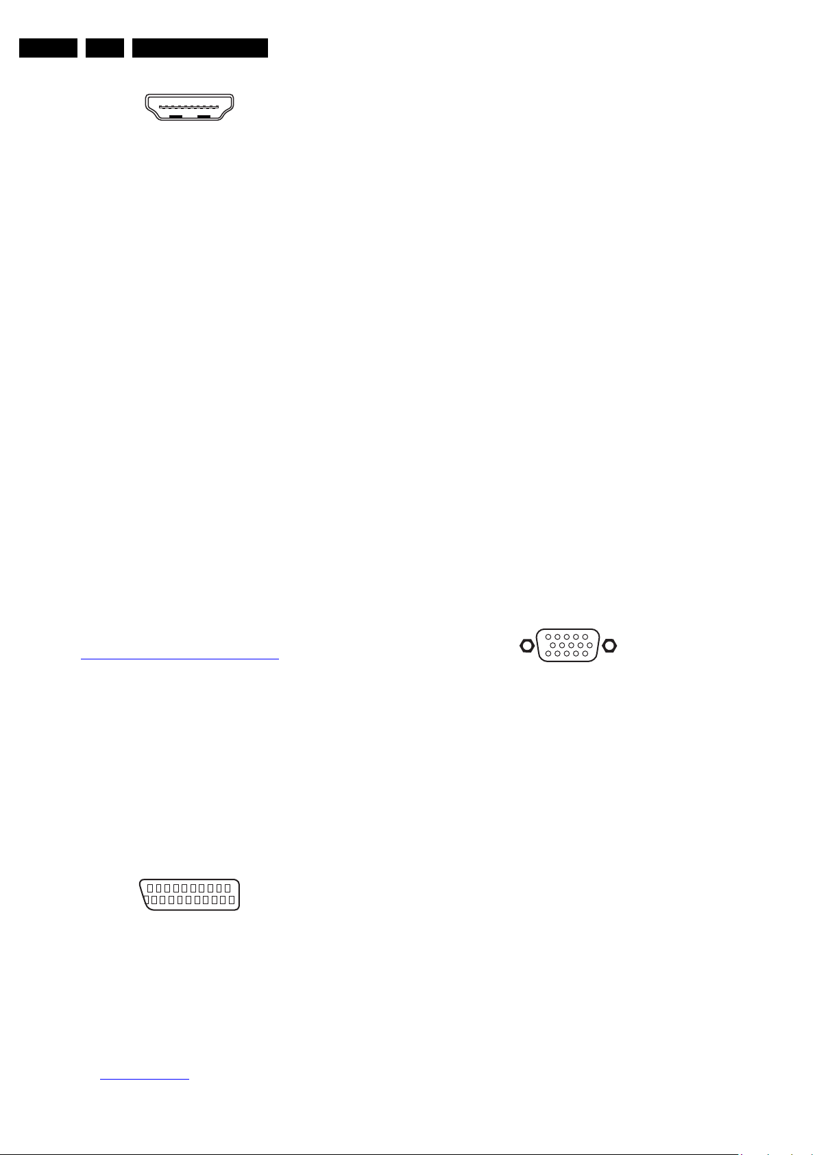
14 - PC IN:VGA
6 - HDMI 1: Digital Video, Digital Audio - In
See 5 - HDMI: Digital Video, Digital Audio - In
.
7 - Cinch: Digital Audio - In
Bk - Coaxial 0.4 - 0.6V
/ 75 Ω j
PP
8 - EXT2: Video YPbPr - In, Audio - In
Gn - Video - Y 1 V
Bu - Video - Pb 0.7 V
Rd - Video - Pr 0.7 V
Wh - Audio - L 0.5 V
Rd - Audio - R 0.5 V
/ 75 W jq
PP
/ 75 W jq
PP
/ 75 W jq
PP
/ 10 kW jq
RMS
/ 10 kW jq
RMS
9 - EXT1 - 2: Video RGB/YC - In, CVBS - In/Out, Audio In/Out
Figure 2-6 SCART connector
1 - Audio R 0.5 V
2 - Audio R 0.5 V
3 - Audio L 0.5 V
/ 1 kΩ k
RMS
/ 10 kΩ j
RMS
/ 1 kΩ k
RMS
Figure 2-7 VGA connector
1 - Video Red 0.7 V
2 - Video Green 0.7 V
3 - Video Blue 0.7 V
4-n.c.
/ 75 W j
PP
/ 75 W j
PP
/ 75 W j
PP
5 - Ground Gnd H
6 - Ground Red Gnd H
7 - Ground Green Gnd H
8 - Ground Blue Gnd H
9-+5V
10 - Ground Sync Gnd H
+5 V j
DC
11 - Ground Red Gnd H
12 - DDC_SDA DDC data j
13 - H-sync 0 - 5 V j
14 - V-sync 0 - 5 V j
15 - DDC_SCL DDC clock j
17 - Mini Jack: IR Link (if present)
1 - Ground Gnd H
2-OIRI-IS j
2-OIRI-IN k
2.4 Chassis Overview
Refer to 9. Block Diagrams for PWB/CBA locations.
2010-Jun-18

Precautions, Notes, and Abbreviation List
3. Precautions, Notes, and Abbreviation List
EN 7TPM2.1E LA 3.
Index of this chapter:
3.1
Safety Instructions
3.2 Warnings
3.3 Notes
3.4 Abbreviation List
3.1 Safety Instructions
Safety regulations require the following during a repair:
• Connect the set to the Mains/AC Power via an isolation
transformer (> 800 VA).
• Replace safety components, indicated by the symbol h,
only by components identical to the original ones. Any
other component substitution (other than original type) may
increase risk of fire or electrical shock hazard.
Safety regulations require that after a repair, the set must be
returned in its original condition. Pay in particular attention to
the following points:
• Route the wire trees correctly and fix them with the
mounted cable clamps.
• Check the insulation of the Mains/AC Power lead for
external damage.
• Check the strain relief of the Mains/AC Power cord for
proper function.
• Check the electrical DC resistance between the Mains/AC
Power plug and the secondary side (only for sets that have
a Mains/AC Power isolated power supply):
1. Unplug the Mains/AC Power cord and connect a wire
between the two pins of the Mains/AC Power plug.
2. Set the Mains/AC Power switch to the “on” position
(keep the Mains/AC Power cord unplugged!).
3. Measure the resistance value between the pins of the
Mains/AC Power plug and the metal shielding of the
tuner or the aerial connection on the set. The reading
should be between 4.5 MΩ and 12 MΩ.
4. Switch “off” the set, and remove the wire between the
two pins of the Mains/AC Power plug.
• Check the cabinet for defects, to prevent touching of any
inner parts by the customer.
• Where necessary, measure the waveforms and voltages
with (D) and without (E) aerial signal. Measure the
voltages in the power supply section both in normal
operation (G) and in stand-by (F). These values are
indicated by means of the appropriate symbols.
3.3.2 Schematic Notes
• All resistor values are in ohms, and the value multiplier is
often used to indicate the decimal point location (e.g. 2K2
indicates 2.2 kΩ).
• Resistor values with no multiplier may be indicated with
either an “E” or an “R” (e.g. 220E or 220R indicates 220 Ω).
• All capacitor values are given in micro-farads (μ=× 10
nano-farads (n =× 10
• Capacitor values may also use the value multiplier as the
decimal point indication (e.g. 2p2 indicates 2.2 pF).
•An “asterisk” (*) indicates component usage varies. Refer
to the diversity tables for the correct values.
• The correct component values are listed on the Philips
Spare Parts Web Portal.
3.3.3 Spare Parts
For the latest spare part overview, consult your Philips Spare
Part web portal.
3.3.4 BGA (Ball Grid Array) ICs
Introduction
For more information on how to handle BGA devices, visit this
URL: http://www.atyourservice-magazine.com
“Magazine”, then go to “Repair downloads”. Here you will find
Information on how to deal with BGA-ICs.
BGA Temperature Profiles
For BGA-ICs, you must use the correct temperature-profile.
Where applicable and available, this profile is added to the IC
Data Sheet information section in this manual.
-9
), or pico-farads (p =× 10
. Select
-12
-6
),
).
3.2 Warnings
• All ICs and many other semiconductors are susceptible to
electrostatic discharges (ESD w). Careless handling
during repair can reduce life drastically. Make sure that,
during repair, you are connected with the same potential as
the mass of the set by a wristband with resistance. Keep
components and tools also at this same potential.
• Be careful during measurements in the high voltage
section.
• Never replace modules or other components while the unit
is switched “on”.
• When you align the set, use plastic rather than metal tools.
This will prevent any short circuits and the danger of a
circuit becoming unstable.
3.3 Notes
3.3.1 General
• Measure the voltages and waveforms with regard to the
chassis (= tuner) ground (H), or hot ground (I), depending
on the tested area of circuitry. The voltages and waveforms
shown in the diagrams are indicative. Measure them in the
Service Default Mode with a colour bar signal and stereo
sound (L: 3 kHz, R: 1 kHz unless stated otherwise) and
picture carrier at 475.25 MHz for PAL, or 61.25 MHz for
NTSC (channel 3).
3.3.5 Lead-free Soldering
Due to lead-free technology some rules have to be respected
by the workshop during a repair:
• Use only lead-free soldering tin. If lead-free solder paste is
required, please contact the manufacturer of your soldering
equipment. In general, use of solder paste within
workshops should be avoided because paste is not easy to
store and to handle.
• Use only adequate solder tools applicable for lead-free
soldering tin. The solder tool must be able:
– To reach a solder-tip temperature of at least 400°C.
– To stabilize the adjusted temperature at the solder-tip.
– To exchange solder-tips for different applications.
• Adjust your solder tool so that a temperature of around
360°C - 380°C is reached and stabilized at the solder joint.
Heating time of the solder-joint should not exceed ~ 4 sec.
Avoid temperatures above 400°C, otherwise wear-out of
tips will increase drastically and flux-fluid will be destroyed.
To avoid wear-out of tips, switch “off” unused equipment or
reduce heat.
• Mix of lead-free soldering tin/parts with leaded soldering
tin/parts is possible but PHILIPS recommends strongly to
avoid mixed regimes. If this cannot be avoided, carefully
clear the solder-joint from old tin and re-solder with new tin.
3.3.6 Alternative BOM identification
It should be noted that on the European Service website,
“Alternative BOM” is referred to as “Design variant”.
2010-Jun-18
EN 8 TPM2.1E LA3.
Precautions, Notes, and Abbreviation List
The third digit in the serial number (example:
AG2B0335000001) indicates the number of the alternative
B.O.M. (Bill Of Materials) that has been used for producing the
specific TV set. In general, it is possible that the same TV
model on the market is produced with e.g. two different types
of displays, coming from two different suppliers. This will then
result in sets which have the same CTN (Commercial Type
Number; e.g. 28PW9515/12) but which have a different B.O.M.
number.
By looking at the third digit of the serial number, one can
identify which B.O.M. is used for the TV set he is working with.
If the third digit of the serial number contains the number “1”
(example: AG1B033500001), then the TV set has been
manufactured according to B.O.M. number 1. If the third digit is
a “2” (example: AG2B0335000001), then the set has been
produced according to B.O.M. no. 2. This is important for
ordering the correct spare parts!
For the third digit, the numbers 1...9 and the characters A...Z
can be used, so in total: 9 plus 26= 35 different B.O.M.s can be
indicated by the third digit of the serial number.
Identification: The bottom line of a type plate gives a 14-digit
serial number. Digits 1 and 2 refer to the production centre (e.g.
AG is Bruges), digit 3 refers to the B.O.M. code, digit 4 refers
to the Service version change code, digits 5 and 6 refer to the
production year, and digits 7 and 8 refer to production week (in
example below it is 2006 week 17). The 6 last digits contain the
serial number.
MODEL :
PROD.NO:
32PF9968/10
AG 1A0617 000001
MADE IN BELGIUM
220-240V 50/60Hz
VHF+S+H+UHF
S
10000_024_090121.eps
~
BJ3.0E LA
Figure 3-1 Serial number (example)
3.3.7 Board Level Repair (BLR) or Component Level Repair (CLR)
If a board is defective, consult your repair procedure to decide
if the board has to be exchanged or if it should be repaired on
component level.
If your repair procedure says the board should be exchanged
completely, do not solder on the defective board. Otherwise, it
cannot be returned to the O.E.M. supplier for back charging!
3.3.8 Practical Service Precautions
• It makes sense to avoid exposure to electrical shock.
While some sources are expected to have a possible
dangerous impact, others of quite high potential are of
limited current and are sometimes held in less regard.
• Always respect voltages. While some may not be
dangerous in themselves, they can cause unexpected
reactions that are best avoided. Before reaching into a
powered TV set, it is best to test the high voltage insulation.
It is easy to do, and is a good service precaution.
128W
100105
3.4 Abbreviation List
0/6/12 SCART switch control signal on A/V
board. 0 = loop through (AUX to TV),
6 = play 16 : 9 format, 12 = play 4 : 3
format
AARA Automatic Aspect Ratio Adaptation:
algorithm that adapts aspect ratio to
remove horizontal black bars; keeps
the original aspect ratio
ACI Automatic Channel Installation:
algorithm that installs TV channels
directly from a cable network by
means of a predefined TXT page
ADC Analogue to Digital Converter
AFC Automatic Frequency Control: control
signal used to tune to the correct
frequency
AGC Automatic Gain Control: algorithm that
controls the video input of the feature
box
AM Amplitude Modulation
AP Asia Pacific
AR Aspect Ratio: 4 by 3 or 16 by 9
ASF Auto Screen Fit: algorithm that adapts
aspect ratio to remove horizontal black
bars without discarding video
information
ATSC Advanced Television Systems
Committee, the digital TV standard in
the USA
ATV See Auto TV
Auto TV A hardware and software control
system that measures picture content,
and adapts image parameters in a
dynamic way
AV External Audio Video
AVC Audio Video Controller
AVIP Audio Video Input Processor
B/G Monochrome TV system. Sound
carrier distance is 5.5 MHz
BDS Business Display Solutions (iTV)
BLR Board-Level Repair
BTSC Broadcast Television Standard
Committee. Multiplex FM stereo sound
system, originating from the USA and
used e.g. in LATAM and AP-NTSC
countries
B-TXT Blue TeleteXT
C Centre channel (audio)
CEC Consumer Electronics Control bus:
remote control bus on HDMI
connections
CL Constant Level: audio output to
connect with an external amplifier
CLR Component Level Repair
ComPair Computer aided rePair
CP Connected Planet / Copy Protection
CSM Customer Service Mode
CTI Color Transient Improvement:
manipulates steepness of chroma
transients
CVBS Composite Video Blanking and
Synchronization
DAC Digital to Analogue Converter
DBE Dynamic Bass Enhancement: extra
low frequency amplification
DCM Data Communication Module. Also
referred to as System Card or
Smartcard (for iTV).
DDC See “E-DDC”
D/K Monochrome TV system. Sound
carrier distance is 6.5 MHz
DFI Dynamic Frame Insertion
2010-Jun-18

Precautions, Notes, and Abbreviation List
EN 9TPM2.1E LA 3.
DFU Directions For Use: owner's manual
DMR Digital Media Reader: card reader
DMSD Digital Multi Standard Decoding
DNM Digital Natural Motion
DNR Digital Noise Reduction: noise
reduction feature of the set
DRAM Dynamic RAM
DRM Digital Rights Management
DSP Digital Signal Processing
DST Dealer Service Tool: special remote
control designed for service
technicians
DTCP Digital Transmission Content
Protection; A protocol for protecting
digital audio/video content that is
traversing a high speed serial bus,
such as IEEE-1394
DVB-C Digital Video Broadcast - Cable
DVB-T Digital Video Broadcast - Terrestrial
DVD Digital Versatile Disc
DVI(-d) Digital Visual Interface (d= digital only)
E-DDC Enhanced Display Data Channel
(VESA standard for communication
channel and display). Using E-DDC,
the video source can read the EDID
information form the display.
EDID Extended Display Identification Data
(VESA standard)
EEPROM Electrically Erasable and
Programmable Read Only Memory
EMI Electro Magnetic Interference
EPG Electronic Program Guide
EPLD Erasable Programmable Logic Device
EU Europe
EXT EXTernal (source), entering the set by
SCART or by cinches (jacks)
FDS Full Dual Screen (same as FDW)
FDW Full Dual Window (same as FDS)
FLASH FLASH memory
FM Field Memory or Frequency
Modulation
FPGA Field-Programmable Gate Array
FTV Flat TeleVision
Gb/s Giga bits per second
G-TXT Green TeleteXT
H H_sync to the module
HD High Definition
HDD Hard Disk Drive
HDCP High-bandwidth Digital Content
Protection: A “key” encoded into the
HDMI/DVI signal that prevents video
data piracy. If a source is HDCP coded
and connected via HDMI/DVI without
the proper HDCP decoding, the
picture is put into a “snow vision” mode
or changed to a low resolution. For
normal content distribution the source
and the display device must be
enabled for HDCP “software key”
decoding.
HDMI High Definition Multimedia Interface
HP HeadPhone
I Monochrome TV system. Sound
2
I
C Inter IC bus
2
I
D Inter IC Data bus
2
I
S Inter IC Sound bus
carrier distance is 6.0 MHz
IF Intermediate Frequency
IR Infra Red
IRQ Interrupt Request
ITU-656 The ITU Radio communication Sector
(ITU-R) is a standards body
subcommittee of the International
Telecommunication Union relating to
radio communication. ITU-656 (a.k.a.
SDI), is a digitized video format used
for broadcast grade video.
Uncompressed digital component or
digital composite signals can be used.
The SDI signal is self-synchronizing,
uses 8 bit or 10 bit data words, and has
a maximum data rate of 270 Mbit/s,
with a minimum bandwidth of 135
MHz.
ITV Institutional TeleVision; TV sets for
hotels, hospitals etc.
LS Last Status; The settings last chosen
by the customer and read and stored
in RAM or in the NVM. They are called
at start-up of the set to configure it
according to the customer's
preferences
LATAM Latin America
LCD Liquid Crystal Display
LED Light Emitting Diode
L/L' Monochrome TV system. Sound
carrier distance is 6.5 MHz. L' is Band
I, L is all bands except for Band I
LPL LG.Philips LCD (supplier)
LS Loudspeaker
LVDS Low Voltage Differential Signalling
Mbps Mega bits per second
M/N Monochrome TV system. Sound
carrier distance is 4.5 MHz
MHEG Part of a set of international standards
related to the presentation of
multimedia information, standardised
by the Multimedia and Hypermedia
Experts Group. It is commonly used as
a language to describe interactive
television services
MIPS Microprocessor without Interlocked
Pipeline-Stages; A RISC-based
microprocessor
MOP Matrix Output Processor
MOSFET Metal Oxide Silicon Field Effect
Transistor, switching device
MPEG Motion Pictures Experts Group
MPIF Multi Platform InterFace
MUTE MUTE Line
MTV Mainstream TV: TV-mode with
Consumer TV features enabled (iTV)
NC Not Connected
NICAM Near Instantaneous Compounded
Audio Multiplexing. This is a digital
sound system, mainly used in Europe.
NTC Negative Temperature Coefficient,
non-linear resistor
NTSC National Television Standard
Committee. Color system mainly used
in North America and Japan. Color
carrier NTSC M/N= 3.579545 MHz,
NTSC 4.43= 4.433619 MHz (this is a
VCR norm, it is not transmitted off-air)
NVM Non-Volatile Memory: IC containing
TV related data such as alignments
O/C Open Circuit
OSD On Screen Display
OAD Over the Air Download. Method of
software upgrade via RF transmission.
Upgrade software is broadcasted in
TS with TV channels.
OTC On screen display Teletext and
Control; also called Artistic (SAA5800)
P50 Project 50: communication protocol
between TV and peripherals
PAL Phase Alternating Line. Color system
mainly used in West Europe (color
carrier= 4.433619 MHz) and South
America (color carrier PAL M=
2010-Jun-18

EN 10 TPM2.1E LA3.
Precautions, Notes, and Abbreviation List
3.575612 MHz and PAL N= 3.582056
MHz)
PCB Printed Circuit Board (same as “PWB”)
PCM Pulse Code Modulation
PDP Plasma Display Panel
PFC Power Factor Corrector (or Pre-
conditioner)
PIP Picture In Picture
PLL Phase Locked Loop. Used for e.g.
FST tuning systems. The customer
can give directly the desired frequency
POD Point Of Deployment: a removable
CAM module, implementing the CA
system for a host (e.g. a TV-set)
POR Power On Reset, signal to reset the uP
PSDL Power Supply for Direct view LED
backlight with 2D-dimming
PSL Power Supply with integrated LED
drivers
PSLS Power Supply with integrated LED
drivers with added Scanning
functionality
PTC Positive Temperature Coefficient,
non-linear resistor
PWB Printed Wiring Board (same as “PCB”)
PWM Pulse Width Modulation
QRC Quasi Resonant Converter
QTNR Quality Temporal Noise Reduction
QVCP Quality Video Composition Processor
RAM Random Access Memory
RGB Red, Green, and Blue. The primary
color signals for TV. By mixing levels
of R, G, and B, all colors (Y/C) are
reproduced.
RC Remote Control
RC5 / RC6 Signal protocol from the remote
control receiver
RESET RESET signal
ROM Read Only Memory
RSDS Reduced Swing Differential Signalling
data interface
R-TXT Red TeleteXT
SAM Service Alignment Mode
S/C Short Circuit
SCART Syndicat des Constructeurs
d'Appareils Radiorécepteurs et
Téléviseurs
SCL Serial Clock I
SCL-F CLock Signal on Fast I
SD Standard Definition
SDA Serial Data I
SDA-F DAta Signal on Fast I
2
C
2
C bus
2
C
2
C bus
SDI Serial Digital Interface, see “ITU-656”
SDRAM Synchronous DRAM
SECAM SEequence Couleur Avec Mémoire.
Color system mainly used in France
and East Europe. Color carriers=
4.406250 MHz and 4.250000 MHz
SIF Sound Intermediate Frequency
SMPS Switched Mode Power Supply
SoC System on Chip
SOG Sync On Green
SOPS Self Oscillating Power Supply
SPI Serial Peripheral Interface bus; a 4-
wire synchronous serial data link
standard
S/PDIF Sony Philips Digital InterFace
SRAM Static RAM
SRP Service Reference Protocol
SSB Small Signal Board
SSC Spread Spectrum Clocking, used to
reduce the effects of EMI
STB Set Top Box
STBY STand-BY
SVGA 800 × 600 (4:3)
SVHS Super Video Home System
SW Software
SWAN Spatial temporal Weighted Averaging
Noise reduction
SXGA 1280 × 1024
TFT Thin Film Transistor
THD Total Harmonic Distortion
TMDS Transmission Minimized Differential
Signalling
TS Transport Stream
TXT TeleteXT
TXT-DW Dual Window with TeleteXT
UI User Interface
uP Microprocessor
UXGA 1 600 × 1 200 (4:3)
V V-sync to the module
VESA Video Electronics Standards
Association
VGA 640 × 480 (4:3)
VL Variable Level out: processed audio
output toward external amplifier
VSB Vestigial Side Band; modulation
method
WYSIWYR What You See Is What You Record:
record selection that follows main
picture and sound
WXGA 1280 × 768 (15:9)
XTAL Quartz crystal
XGA 1024 × 768 (4:3)
Y Luminance signal
Y/C Luminance (Y) and Chrominance (C)
signal
YPbPr Component video. Luminance and
scaled color difference signals (B-Y
and R-Y)
YUV Component video
2010-Jun-18
4. Mechanical Instructions
18290_100_090227.eps
100104
Mechanical Instructions
EN 11TPM2.1E LA 4.
Index of this chapter:
4.1
Cable Dressing
4.2 Service Positions
4.3 Assy/Panel Removal Click Styling
4.4 Assy/Panel Removal P&S Styling
4.5 Set Re-assembly.
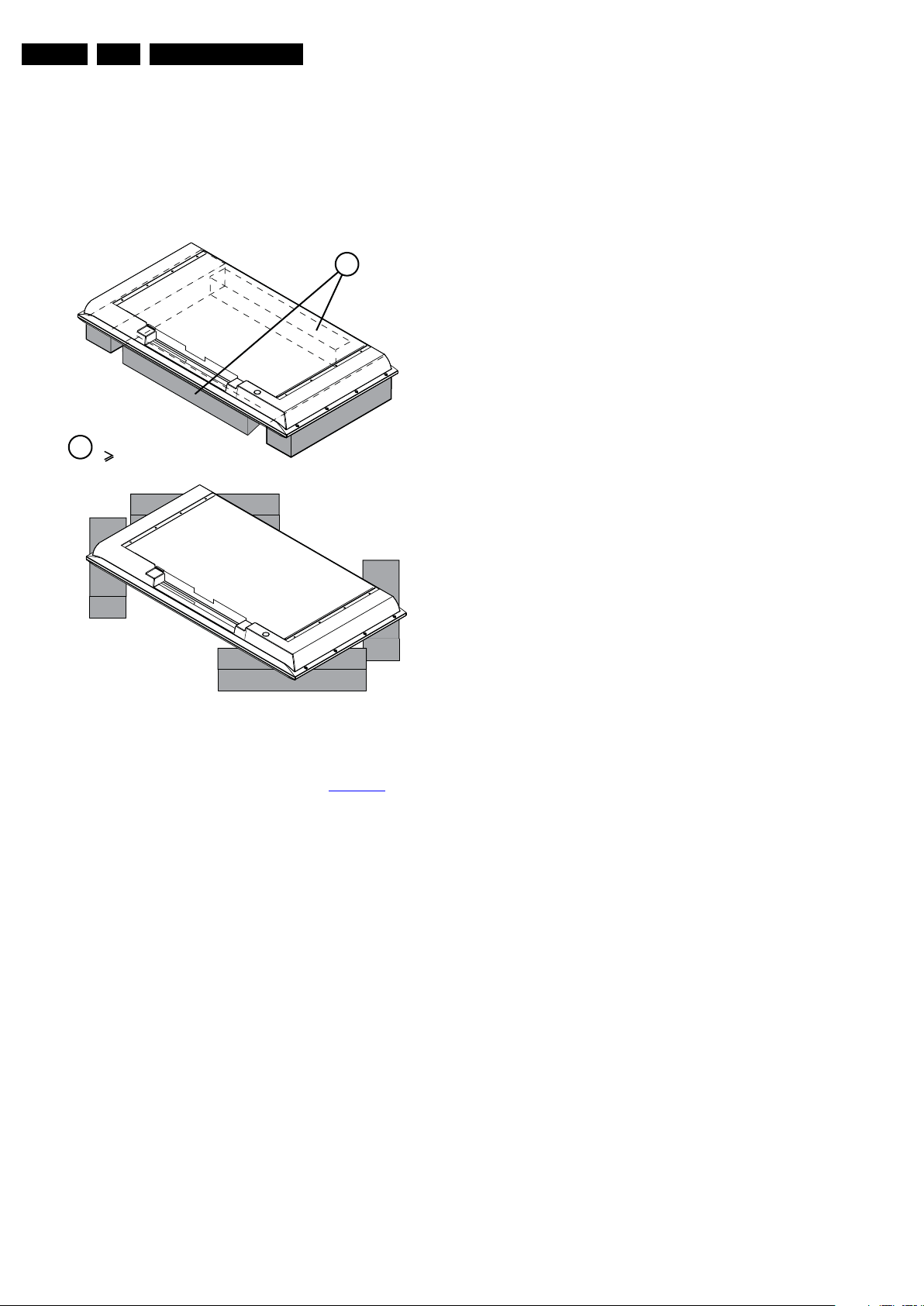
4.1 Cable Dressing
Notes:
• Figures below can deviate slightly from the actual situation,
due to the different set executions.
Figure 4-1 Cable dressing 19" and 22" Click
2010-Jun-18
EN 12 TPM2.1E LA4.
18291_100_090906.eps
100104
1
8290_101_090330.eps
091005
Mechanical Instructions
Figure 4-2 Cable dressing 22" P & S
2010-Jun-18
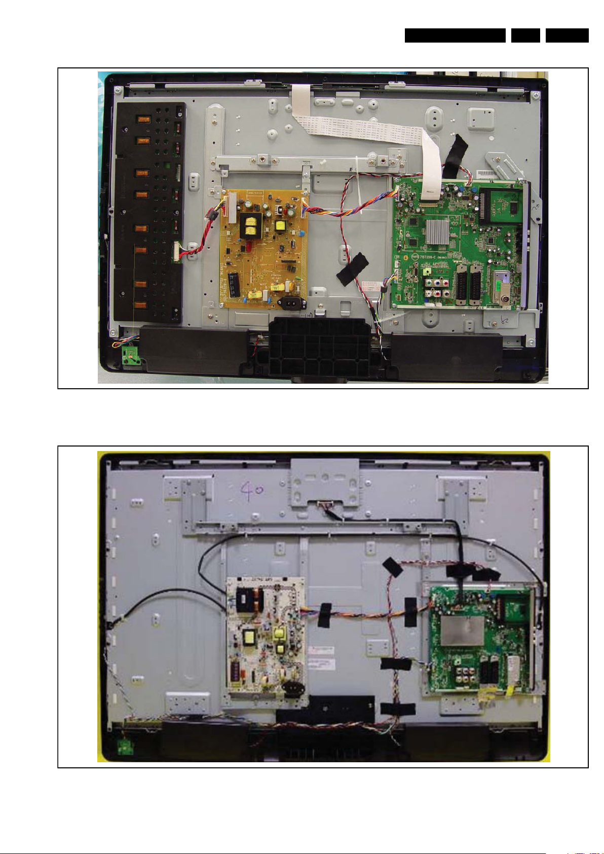
Figure 4-3 Cable dressing 26" Click
Mechanical Instructions
18291_101_090609.eps
100105
1
8291_102_090609.eps
100105
EN 13TPM2.1E LA 4.
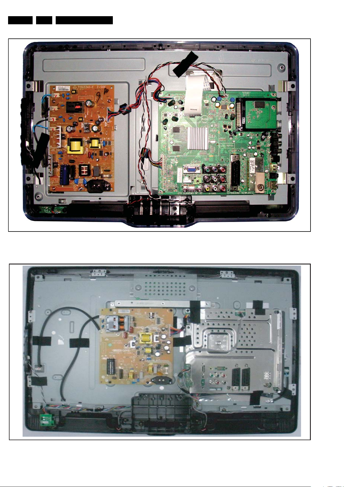
Figure 4-4 Cable dressing 32" Click
Figure 4-5 Cable dressing 42" Click
2010-Jun-18
EN 14 TPM2.1E LA4.
18292_105_090710.eps
100106
18292_106_090710.eps
100106
Mechanical Instructions
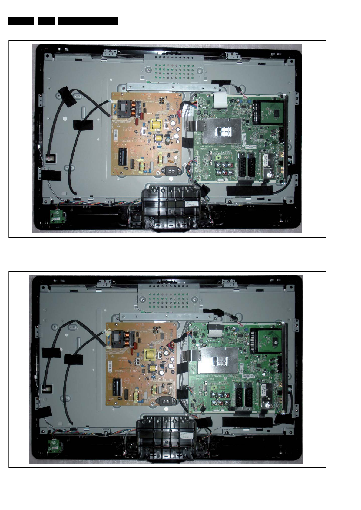
Figure 4-6 Cable dressing 26HFL3331D
2010-Jun-18
Figure 4-7 Cable dressing 26HFL4371D
Mechanical Instructions
18292_107_090710.eps
100106
EN 15TPM2.1E LA 4.
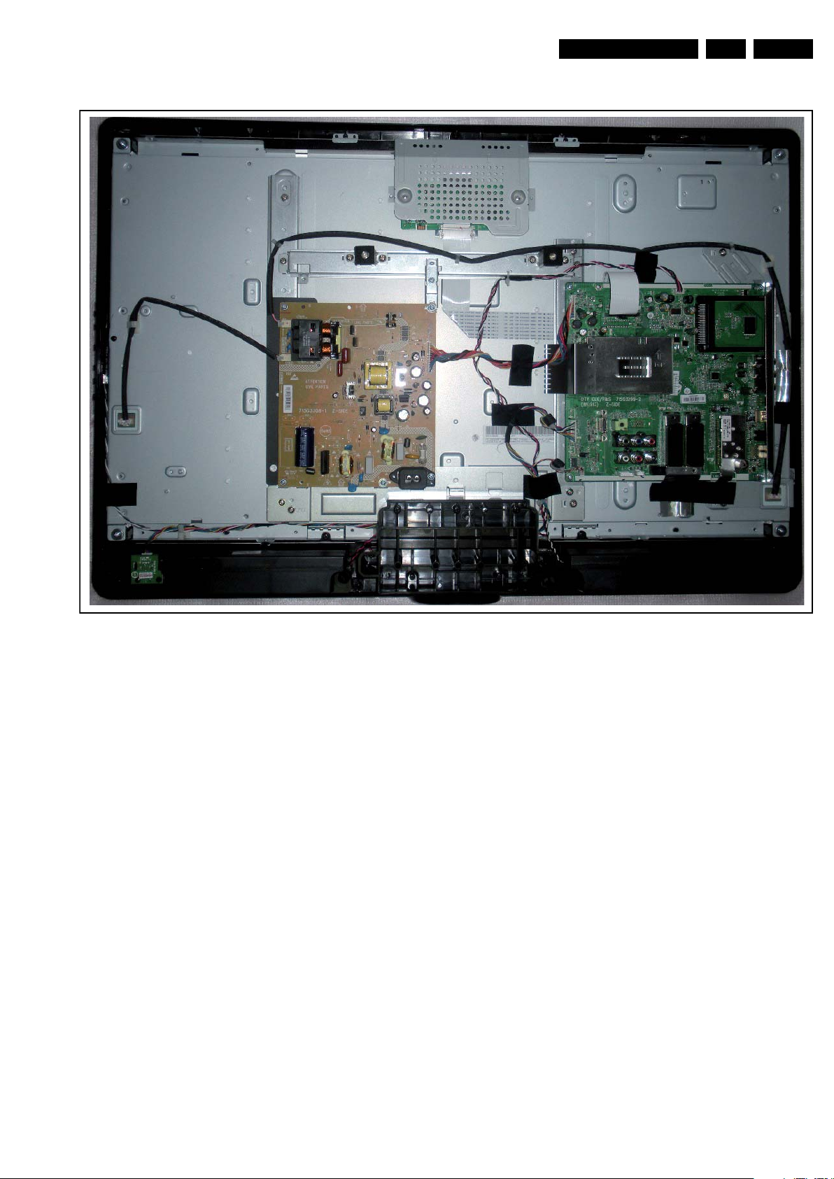
Figure 4-8 Cable dressing 32HFL4351D
2010-Jun-18
EN 16 TPM2.1E LA4.
10000_018_090121.eps
090121
1
Required for sets
42"
1
Mechanical Instructions
4.2 Service Positions
For easy servicing of this set, there are a few possibilities
created:
• The buffers from the packaging.
• Foam bars (created for Service).
4.2.1 Foam Bars
4.3 Assy/Panel Removal Click Styling
4.3.1 Rear Cover
Warning: Disconnect the mains power cord before removing
the rear cover.
1. Remove the fixation screws that secure the rear cover.
2. Lift the rear cover from the TV. Make sure that wires and
flat foils are not damaged while lifting the rear cover from
the set.
4.3.2 Small Signal Board (SSB)
Caution: it is mandatory to remount all different screws at their
original position during re-assembly. Failure to do so may result
in damaging the SSB.
1. Release the screws to remove the shielding.
2. Unplug both LVDS connector.
Caution: be careful, as these are very fragile connectors!
3. Unplug all other connectors.
4. Remove the screw near the L- AUDIO- R at the side I/O
cover.
5. Remove the rest of the fixation screws.
6. The SSB can now be taken out of the set.
4.3.3 Power Supply Unit (PSU)
Caution: it is mandatory to remount all different screws at their
original position during re-assembly. Failure to do so may result
in damaging the PSU.
1. Unplug all connectors.
2. Remove all fixation screws.
3. The PSU can now be taken out of the set.
When defective, replace the whole unit.
The foam bars (order code 3122 785 90580 for two pieces) can
be used for all types and sizes of Flat TVs. See Figure 4-9
details. Sets with a display of 42" and larger, require four foam
bars [1]. Ensure that the foam bars are always supporting the
cabinet and never only the display.
Caution: Failure to follow these guidelines can seriously
damage the display!
By laying the TV face down on the (ESD protective) foam bars,
a stable situation is created to perform measurements and
alignments. By placing a mirror under the TV, the screen can
be monitored.
Figure 4-9 Foam bars
4.3.4 Keyboard Control Panel
1. Unplug the connector.
2. Remove the cover screws and take out the whole unit.
When defective, replace the whole unit.
4.3.5 IR Board
for
1. Remove screw and lift the IR Board from the front cover.
2. Unplug the connectors.
When defective, replace the whole unit.
4.3.6 Speakers
1. Release the speaker connector from the unit.
2. Take the speakers out together with their casing.
When defective, replace the whole unit.
4.3.7 LCD Panel
1. Remove the speakers as described earlier.
2. Unplug the LVDS connector.
3. Remove the fixation screws that fix panel to the subframe.
4. Lift out the subframe.
5. The LCD panel can now be lifted from the front cabinet.
When defective, replace the whole unit.
2010-Jun-18

Mechanical Instructions
EN 17TPM2.1E LA 4.
4.4 Assy/Panel Removal P&S Styling
4.4.1 Rear Cover
Warning: Disconnect the mains power cord before removing
the rear cover.
1. Remove the fixation screws that secure the rear cover.
2. Lift the rear cover from the TV. Make sure that wires and
flat foils are not damaged while lifting the rear cover from
the set.
4.4.2 Small Signal Board (SSB)
Caution: it is mandatory to remount all different screws at their
original position during re-assembly. Failure to do so may result
in damaging the SSB.
1. Remove the screws that fix VGA connector.
2. Release the rest screws to remove the shielding.
3. Unplug both LVDS connector.
Caution: be careful, as these are very fragile connectors!
4. Unplug all other connectors.
5. The SSB can now be taken out of the set.
4.4.3 Power Supply Unit (PSU)
Caution: it is mandatory to remount all different screws at their
original position during re-assembly. Failure to do so may result
in damaging the PSU.
1. Unplug all connectors.
2. Remove all fixation screws.
3. The PSU can now be taken out of the set.
When defective, replace the whole unit.
4.5 Set Re-assembly
To re-assemble the whole set, execute all processes in reverse
order.
Notes:
• While re-assembling, make sure that all cables are placed
and connected in their original position. See Figure 4-1
Figure 4-2
• Pay special attention not to damage the EMC foams on the
SSB shields. Ensure that EMC foams are mounted
correctly.
, Figure 4-3, Figure 4-4 and Figure 4-5.
,
4.4.4 Keyboard Control Panel
1. Take the keyboard control assy out of the bezel.
2. Unplug the connector.
3. Remove the cover screws and take out the whole unit.
When defective, replace the whole unit.
4.4.5 IR Board
1. Remove screws and lift the IR Board from the front cover.
2. Unplug the connectors.
When defective, replace the whole unit.
4.4.6 Speakers
1. Release the speaker connector from the SSB.
2. Take the speakers out together with their casing.
When defective, replace the whole unit.
4.4.7 LCD Panel
1. Remove the speakers as described earlier.
2. Unplug the LVDS connector.
3. Remove the fixation screws that fix panel to the subframe.
4. Lift out the subframe.
5. The LCD panel can now be lifted from the front cabinet.
When defective, replace the whole unit.
2010-Jun-18
EN 18 TPM2.1E LA5.
Service Modes, Error Codes, and Fault Finding
5. Service Modes, Error Codes, and Fault Finding
Index of this chapter:
5.1
Test Points
5.2 Service Modes
5.3 Service Tools
5.4 Error Codes
5.5 Fault Finding and Repair Tips
5.1 Test Points
As most signals are digital, it will be difficult to measure
waveforms with a standard oscilloscope. However, several key
ICs are capable of generating test patterns, which can be
controlled via ComPair. In this way it is possible to determine
which part is defective.
Perform measurements under the following conditions:
• Service Default Mode.
• Video: Colour bar signal.
• Audio: 1 kHz
5.2 Service Modes
Service Default mode (SDM) and Service Alignment Mode
(SAM) offers several features for the service technician, while
the Customer Service Mode (CSM) is used for communication
between the call centre and the customer.
This chassis also offers the option of using ComPair, a
hardware interface between a computer and the TV chassis. It
offers the abilities of structured troubleshooting, error code
reading, and software version read-out for all chassis.
(see also section “5.3.1
5.2.1 Service Default Mode (SDM)
Table 5-1 SDM default settings
Region Freq. (MHz) Default system
Europe, PAL 475.25 PAL B/G
Europe, DVB-T 564.000 DVB-T
• All picture settings at 50% (brightness, colour, contrast).
• All sound settings at 50%, except volume at 20%.
• All service-unfriendly modes (if present) are disabled, like:
– (Sleep) timer.
– Child/parental lock.
– Picture mute (blue mute or black mute).
– Automatic volume levelling (AVL).
– Skip/blank of non-favourite pre-sets.
How to Activate SDM
Use the standard RC-transmitter and key in the code “062596”,
directly followed by the “MENU” button.
After activating this mode, “SDM” will appear in the upper right
corner of the screen (when a picture is available).
How to Navigate
When the “MENU” button is pressed on the RC transmitter, the
set will toggle between the SDM and the normal user menu
(with the SDM mode still active in the background).
How to Exit SDM
Press “Power” button on the standard RC-transmitter.
ComPair”)
5.2.2 Service Alignment Mode (SAM)
Purpose
• To perform (software) alignments.
• To change option settings.
• To easily identify the used software version.
• To display (or clear) the error code buffer.
How to Activate SAM
Via a standard RC transmitter: key in the code “062596”
directly followed by the “INFO” button.
Contents of SAM:
• F/W Version. Displays the version of the firmware, Flash
PQ, MTK, MCU and OAD software.
• Panel Type. Displays the type of the panel.
• AUTO_COLOR.
PC: any pattern that has black and white.
YPbPr: SMPTE bar (colour bar), any timing.
• ADC Gain & Offset. There are ADC_GAIN_R,
ADC_GAIN_G, ADC_GAIN_B, ADC_OFFSET_R,
ADC_OFFSET_G, ADC_OFFSET_B. The values (the
range is from 0 to 255) are different by VGA and YPbPr.
• Color Temperature. There are CLR_TEMP_R,
CLR_TEMP_G, CLR_TEMP_B. The values are from 0 to
255. Back-End Scaler R G B Gain. NVM has YPbPr
normal, warm, cool, customer four sets. Other sources use
offset with hard code.
• VIRGIN Mode. Reset the initialization or not.
• GAMMA_TABLE. Use the gamma table or not.
• Error Code. Display the latest 5 error code status.
• Clear Error Buffer. Reset CSM error code to 0.
• NVM COPY TV to USB. To upload several settings from
the TV to an USB stick, which is connected to the SSB. The
items are “Channel list”, “Personal settings
codes”, “Display-related alignments” and “History list”. First
a directory “repair\” has to be created in the root of the USB
stick. To upload the settings select each item separately,
press “cursor right” (or the “OK button), confirm with “OK”
and wait until “Done” appears. In case the download to the
USB stick was not successful “Failure” will appear. In this
case, check if the USB stick is connected properly and if
the directory “repair” is present in the root of the USB stick.
Now the settings are stored onto the USB stick and can be
used to download onto another TV or other SSB.
Uploading is of course only possible if the software is
running and if a picture is available. This method is created
to be able to save the customer’s TV settings and to store
them into another SSB.
• NVM READ USB to TV. To download several settings from
the USB stick to the TV. Same way of working as with
uploading. To make sure that the download of the channel
list from USB to the TV is executed properly, it is necessary
to restart the TV and tune to a valid preset if necessary.
Note: The “History list item” can not be downloaded from
USB to the TV. This is a “read-only” item.
• RESET_PDS_PWD. Clear NVM address.
• VIDEO_PWM_MEDIUM. PWM value at contrast 50%.
• VIDEO_PWM_MINIMUN. PWM minimun value.
• VIDEO_PWM_MAXIMUN. PWM maximun value.
• VIDEO_PWM_RATIO_TOP. PWM value at best power.
• VIDEO_PWM_RATIO_BOTTOM. PWM value at best
picture.
• VGA_PWM_MAXIMUN. Max PWM value in PC mode.
• YPBPR_PHASE. 480i, 480p, 576i, 576p, 720p50, 720p60,
1080i25, 1080i30, 1080p24, 1080p50, 1080p60.
•
AUD_GAIN_LINEIN. Audio gain by different sources.
• AUD_GAIN_HDMI. Audio gain by HDMI.
• AUD_GAIN_ATV. Audio gain by ATV.
• AUD_GAIN_DTV. Audio gain by DTV.
• AUD_GAIN_USB. Audio gain by USB.
”, “Option
2010-Jun-18

Service Modes, Error Codes, and Fault Finding
EN 19TPM2.1E LA 5.
• AUD_LIPSYNC_SPK. The range is from 0 to 80ms, the
unit of the value stored into EEPROM shall be
0.147ms/unit. “+” is delay, “-” is ahead. NVW value = delay
(ms) / 0.147. (example: If you want to set it to 40 ms, fill the
NVM with 40 / 0.147 = 272).
• AUD_LIPSYNC_HP. The range is from 0 to 80ms, the unit
of the value stored into EEPROM shall be 0.147ms/unit. “+”
is delay, “-” is ahead. NVW value = delay (ms) / 0.147.
(example: If you want to set it to 40 ms, fill the NVM with
40 / 0.147 = 272).
• AUD_LIPSYNC_SPDIF. The range is from 0 to 80ms, the
unit of the value stored into EEPROM shall be
0.147ms/unit. “+” is delay, “-” is ahead. NVW value = delay
(ms) / 0.147. (example: If you want to set it to 40 ms, fill the
NVM with 40 / 0.147 = 272).
• TUNER _ID. Displays the manufacturer of the tuner. NXP
tuner is identified with 4 while LG is identified with 5.
• AV2 SCART2. 0 indicates not available, 2 indicates CVBS
and YC.
• HDMI 3. 0 indicates OFF, 1 indicates ON.
• HDMI 2. 0 indicates OFF, 1 indicates ON.
• VGA. 0 indicates OFF, 1 indicates ON.
• MHEG5. 0 indicates OFF, 1 indicates ON.
• RESET OPTION CODE for PnS. After reset, should reset
the set immediately.
• RESET OPTION CODE for CLICK. After reset, should
reset the set immediately.
• ESTICKER NVM (0-15). Icon number is from 0 to 61, 255
indicates no icon.
• Production serial number. Philips serial number
• Software version.
Format: TPAA.AA V2.XX_Y_Z
TPAA.AA is the chassis name
V2.XX is the revision (4 letter)
Y is the vendor code (1 digit):
Z is the panel revision code (1 digit)
• Codes. Shows the latest 5 error code (layer 2) status:
000 = No problem, 011 = I
• SSB. Philips 12NC of SSB (small signal board)
• Display. Philips 12NC of the display (LCD panel).
• PSU. Philips 12NC of PSU (Power Supply Unit).
• NVM version. Revision (4 letters).
• PQ version. Revision (4 letters).
How to Exit CSM
Press “MENU” on the RC-transmitter.
2
C bus error, 012 = tuner error
How to Navigate
• In SAM, the menu items can be selected with the
“CURSOR UP/DOWN” key on the RC-transmitter. The
selected item will be highlighted. When not all menu items
fit on the screen, move the “CURSOR UP/DOWN” key to
display the next/previous menu items.
• With the “CURSOR LEFT/RIGHT” keys, it is possible to:
– (De) activate the selected menu item.
– (De) activate the selected sub menu.
• With the “OK” key, it is possible to activate the selected
action.
How to Exit SAM
Press “Power” button on the RC-transmitter.
How to Exit Burn in
Press “Source” button on the RC-transmitter.
5.2.3 Customer Service Mode (CSM)
Purpose
When a customer is having problems with his TV-set, he can
call his dealer or the Customer Helpdesk. The service
technician can then ask the customer to activate the CSM, in
order to identify the status of the set. Now, the service
technician can judge the severity of the complaint. In many
cases, he can advise the customer how to solve the problem,
or he can decide if it is necessary to visit the customer.
The CSM is a read only mode; therefore, modifications in this
mode are not possible.
How to Activate CSM
Key in the code “123654” via the standard RC-transmitter.
Note: Activation of the CSM is only possible if there is no (user)
menu on the screen!
How to Navigate
By means of the “CURSOR-DOWN/UP” key on the RCtransmitter, can be navigated through the menus.
Contents of CSM
• Model. Philips model type.
2010-Jun-18
EN 20 TPM2.1E LA5.
10000_036_090121.eps
091118
TO
UART SERVICE
CONNECTOR
TO
UART SERVICE
CONNECTOR
TO
I2C SERVICE
CONNECTOR
TO TV
PC
HDMI
I
2
C only
Optional power
5V DC
ComPair II Developed by Philips Brugge
RC out
RC in
Optional
Switch
Power ModeLink/
Activity
I
2
C
ComPair II
Multi
function
RS232 /UART
Service Modes, Error Codes, and Fault Finding
5.3 Service Tools
5.3.1 ComPair
Introduction
ComPair (Computer Aided Repair) is a Service tool for Philips
Consumer Electronics products. and offers the following:
1. ComPair helps to quickly get an understanding on how to
repair the chassis in a short and effective way.
2. ComPair allows very detailed diagnostics and is therefore
capable of accurately indicating problem areas. No
knowledge on I
because ComPair takes care of this.
3. ComPair speeds up the repair time since it can
automatically communicate with the chassis (when the uP
is working) and all repair information is directly available.
4. ComPair features TV software up possibilities.
Specifications
ComPair consists of a Windows based fault finding program
and an interface box between PC and the (defective) product.
The ComPair II interface box is connected to the PC via an
USB cable. For the TV chassis, the ComPair interface box and
the TV communicate via a bi-directional cable via the service
connector (s).
The ComPair fault finding program is able to determine the
problem of the defective television, by a combination of
automatic diagnostics and an interactive question/answer
procedure.
2
C or UART commands is necessary,
5.4 Error Codes
The error code buffer contains all detected errors since the last
time the buffer was erased. The buffer is written from left to
right. When an error occurs that is not yet in the error code
buffer, it is displayed at the left side and all other errors shift one
position to the right.
5.5 Fault Finding and Repair Tips
5.5.1 Exit “Factory Mode”
Choose “EXIT”, then press “OK” button. Turn off the TV and
then turn on the TV.
5.5.2 Speakers
Make sure that the volume is set to minimum during
disconnecting the speakers in the ON-state of the TV. The
audio amplifier can be damaged by disconnecting the speakers
during ON-state of the set!
How to Connect
This is described in the chassis fault finding database in
ComPair.
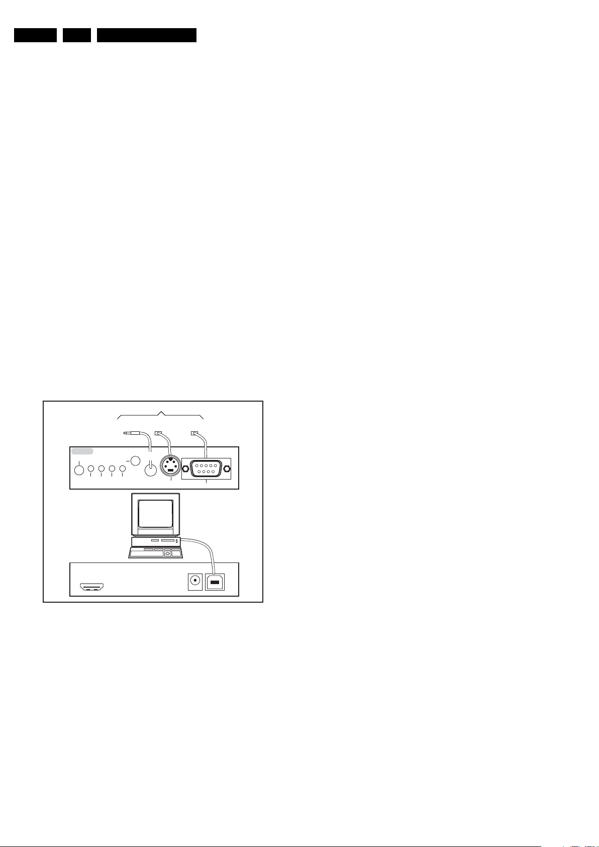
Figure 5-1 ComPair II interface connection
Caution: It is compulsory to connect the TV to the PC as
shown in the picture above (with the ComPair interface in
between), as the ComPair interface acts as a level shifter. If
one connects the TV directly to the PC (via UART), ICs will be
blown!
How to Order
ComPair II order codes:
• ComPair II interface: 3122 785 91020.
• Programming software can be downloaded from the Philips
Service Portal.
• ComPair UART interface cable for TPM2.1x xx.
(using JST PHR-3, 2 mm pitch connector):
3122 785 90630.
Note: While having problems, contact the local support desk.
2010-Jun-18
6. Alignments
Alignments
EN 21TPM2.1E LA 6.
Index of this chapter:
6.1
General Alignment Conditions
6.2 YpbPr Mode Display Adjustment
6.3 PC Mode Adjustment
6.5 Factory Mode Preset
6.6 Serial Number Definition
Note: The Service Default Mode (SDM) and Service Alignment
Mode (SAM) are described in Chapter 5. Menu navigation is
done with the CURSOR UP, DOWN, LEFT or RIGHT keys of
the remote control transmitter.
6.1 General Alignment Conditions
Perform all electrical adjustments under the following
conditions:
• Power supply voltage: 220 - 240 V
• Connect the set to the mains via an isolation transformer
with low internal resistance.
• Allow the set to warm up for approximately 15 minutes.
• Measure voltages and waveforms in relation to correct
ground.
Caution: It is not allowed to use heatsinks as ground.
• Test probe: Ri > 10 MΩ, Ci < 20 pF.
• Use an isolated trimmer/screwdriver to perform
alignments.
/ 50 ± 3 Hz.
AC
6.2 YpbPr Mode Display Adjustment
6.2.1 Equipment Requirements
Minolta CA-210 or Equivalent colour analyser. Quantum Data
Pattern Generator 802G, 802BT or equivalent instrument.
6.2.2 Input requirements
• Input Signal Type: YPbPr signal
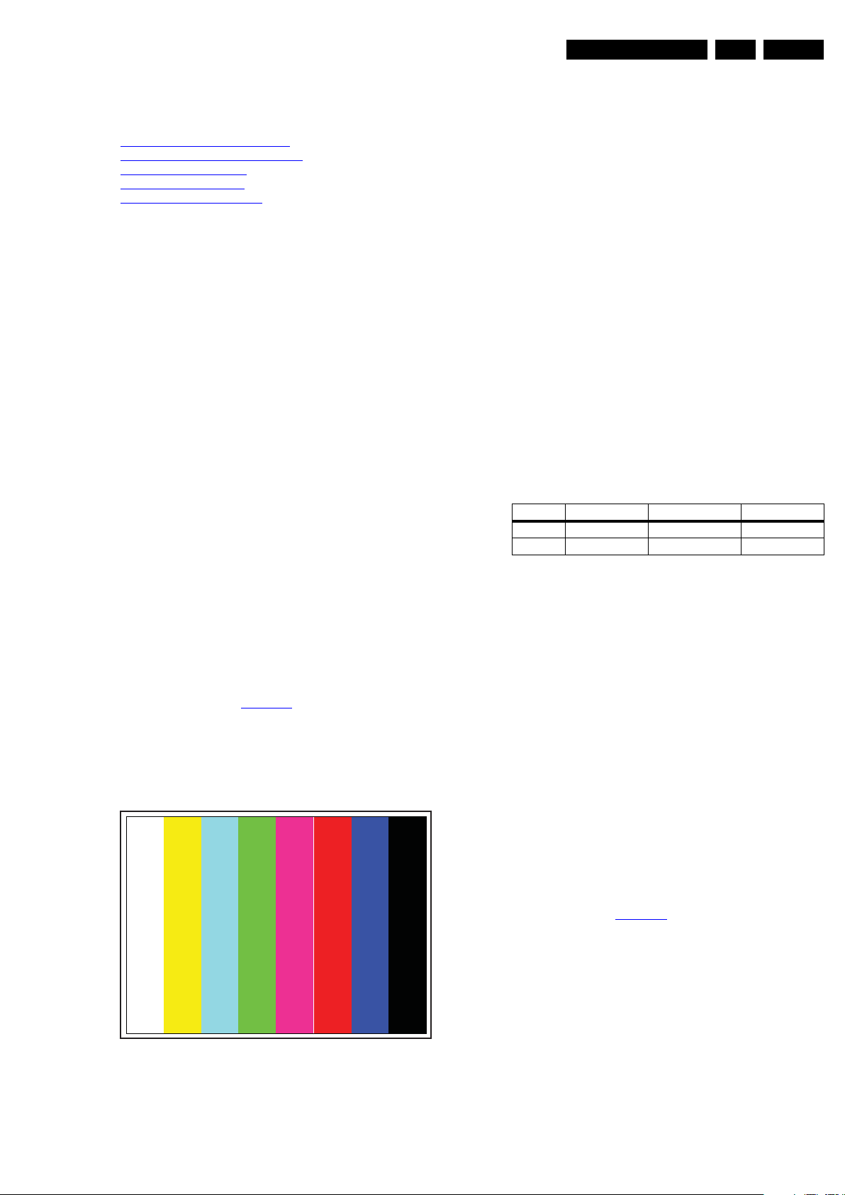
1. 1080i mode, with an YPbPr source, use a 100% colour
bar pattern, see Figure 6-1
scale grey pattern.
2. Select Picture mode to User mode and check the x, y
data.
• Input Signal Strength: 1 V
Pr signal.
• Input Injection Point: YPbPr (RAC jack).
, with a PC source, use a 16-
for Y signal; 0.7 Vpp for Pb and
pp
6.2.3 Alignment method
1. Select source as “YPbPr”.
2. Set Smart picture as “Vivid” and Contrast = 50,
Brightness = 50, colour = 50.
3. Apply a 100% colour bar pattern by a signal generator or
PC.
4. Enter factory mode menu: press numeric keys “062596” +
“INFO” key (SAM mode menu).
6.2.4 Alignment
1. At FAC mode menu, select AUTO_COLOR item. Then
press “OK” key to auto adjust ADC_GAIN_R,
ADC_GAIN_G, ADC_GAIN_B and ADC_OFFSET_R,
ADC_OFFSET_G, ADC_OFFSET_B. Then store those
values to NVM.
2. Set contrast = 80, Brightness = 50 at NORMAL menu
mode.
3. Check the 16 grayscale pattern should be distinguished
and colour bar is correct.
4. Reset AV setting, picture mode shall be recalled to be
“Standard” and Contrast = 80, Brightness = 50.
Table 6-1 White D alignment values
Cool (11000K) Normal (9 000K) Warm (6500K)
x (centre) 0.278 ±0.003 0.289 ±0.003 0.314 ±0.003
y (centre) 0.278 ±0.003 0.291 ±0.003 0.319 ±0.003
Notes:
• Minimum luminance > 280 cd/m2, 350 cd/m2 at the centre
of the screen at Custom colour (Brightness and Contrast
control set at 100%).
• Picture mode should be “Vivid” for outgoing.
• Before measuring, all colour analysers (CA-210) should be
coordinates with a same reference TV set.
• If the colour temperature values are marginal, please use
same equipment and same pattern as in alignment station
for checking.
6.3 PC Mode Adjustment
6.3.1 Equipment Requirements
Minolta CA-210 or Equivalent colour analyser. Chroma 2250 or
equivalent PC signal generator.
Figure 6-1 Colour bar pattern
18290_200_090330.eps
090416
6.3.2 Input requirements
• Input Signal Type: PC VGA signal
1. 1366 * 768@ 60 Hz PC mode with “Five white blocks”
pattern, see Figure 6-2
• Input Signal Strength: 0.7 V
• Input Injection Point: PC D-SUB input
.
linear voltage
pp
2010-Jun-18

EN 22 TPM2.1E LA6.
18290_201_090330.eps
090416
Figure 6-2 Five white blocks pattern
6.3.3 Alignment method
1. Select source as “PC”.
2. Set contrast =80, Brightness=50 at NORMAL menu mode.
3. Apply “5 white block” pattern by VGA pattern generator.
4. Enter factory mode menu: press numeric keys “062596” +
“INFO” key (SAM mode menu).
Alignments
6.3.4 Alignment
1. At FAC mode menu, select AUTO_COLOR item. Then
press “OK” key to auto adjust ADC_GAIN_R,
ADC_GAIN_G, ADC_GAIN_B and ADC_OFFSET_R,
ADC_OFFSET_G, ADC_OFFSET_B. Then store those
values to NVM.
2. Apply flat pattern.
3. Set colour temperature to “NORMAL”.
4. At FAC mode menu, adjust the CLR_TEMP_R,
CLR_TEMP_G, CLR_TEMP_B value to meet “NORMAL”
colour coordinates according to Table 6-1
values to NVM.
5. Repeat step 4 for “COOL” and “WARM”.
6.4 Option Settings
6.4.1 Introduction
The microprocessor communicates with a large number of I
ICs in the set. To ensure good communication and to make
digital diagnosis possible, the microprocessor has to know
which ICs to address. The presence / absence of these specific
ICs (or functions) is made known by the option codes.
Notes:
• After changing the option(s), save them by pressing the OK
button on the RC before the cursor is moved to the left,
select STORE in the SAM root menu and press OK on the
RC.
• The new option setting is only active after the TV is
switched “off” / “stand-by” and “on” again with the Mains
switch (the NVM is then read again).
. Then those
2
C
6.4.2 Reset Options
In SAM, after reset “Reset option code for PnS” and “Reset
option code for click”, restart the set immediately.
2010-Jun-18
6.4.3 Options Menu
Table 6-2 Options menu
Menu-item Subjects Options Description
TV wactching TP speakers On/Off/Auto (EasyLink) Only for PnS model, in non-VGA source
Channel Grid (for all
channels)
Channel Grid (for favourite
channel)
Picture thumbnail browser Silde show Trans. None/Dissolve/Wipe Left/Wipe Right/Wipe Up/Wipe Down/Box In/Box Out Settings for slide show
Photo play back Slide show Trans. None/Dissolve/Wipe Left/Wipe Right/Wipe Up/Wipe Down/Box In/Box Out Settings for slide show
MP3 play back TV speakers On/Off/Auto (EasyLink) Same behavior as via set up menu, only in PnS mode
Video play back TV Speaker On/Off/Auto (EasyLink) Same behavior as via set up menu
Teletext Reveal On/Off
6.4.4 Display Code Overview
Alignments
Mark as favorite Favorites 1/2/3/4 Only in TV source
Show favourite channel Favorites 1/2/3/4, All
Mark as favourite Favorites 1/2/3/4 Only if exist least one channel in channel matrix
Filter channels All/Radio/Digital/Analog
Show favourite channel Favorites 1/2/3/4, All
Slide show Freq. Short/Medium/Long Settings for slide show
Slide show Freq. Short/Medium/Long Settings for slide show
Cycle subpage On/Off Only exist there is subpage teletext
Language Group I/Group II
Full screen Action Only if the page is in dual screen status
EN 23TPM2.1E LA 6.
Table 6-3 Display code overview
CTN_ALT BOM# Panel Type Display Code
19PFL3404D/05_1 LC190WH1TLC1 100
19PFL3404D/12_1 LC190WH1TLC1 100
19PFL3404H/12_1 LC190WH1TLC1 100
19HFL3331D/10_1 LC190WH1TLC1 100
22HFL3331D/10_1 LC220WXETBA1 101
22HFL4371D/10_1 LC220WXETBA1 101
22PFL3404D/05_1 LC220WXETBA1 101
22PFL3404D/12_1 LC220WXETBA1 101
22PFL3404H/12_1 LC220WXETBA1 101
22PFL5604D/12_1 LC215WUETBA1 107
26PFL3404D/05_1 LC260WXESBB1 101
26PFL3404D/12_1 LC260WXESBB1 102
26PFL3404H/12_1 LC260WXESBB1 102
26HFL3331D/10_1 LC260WXESBB1 102
26HFL4371D/10_1 LC260WXESBB1 102
32HFL4351D/10_1 LC320WXE-SBA1_2 105
32PFL3404D/12_1 T315XW02 VR 103
32PFL3404D/12_2 LC320WXE-SBA1_2 105
32PFL3404H/12_1 LC320WXE-SBA1_2 105
42PFL3604D/12_1 T420HW04 V0 104
42PFL3604D/12_2 LC420WUE-SBA1_2 106
42PFL3604H/12_1 LC420WUE-SBA1_2 106
6.5 Factory Mode Preset
Table 6-4 Default Values
Description Setting
VIRGIN_MODE OFF
GAMMA_TABLE ON
COLOR_ENHANCE ON
6.6 Serial Number Definition
Table 6-5 BOM Code
Panel Supplier Code
AUO 1
CPT 2
LPL (LG) 3
QDI 4
CMO 5
HSD 6
SVA 7
2010-Jun-18
EN 24 TPM2.1E LA7.
18290_202_090227.eps
091006
CVBS
MPEG2/4 TS
Nor Flash
512KB
I2C
MCU
DTV reveiver/demodul a tor
MPEG/video/audio decoder
S c a ling
Video enha ncement
3 D comb
LVDS Tr a n smitter
HDMI1.3
ADC
Nan Flash
16/32MB
U S B 2.0
S PDIF Ou t
LVDS to pa nel
RC
Keys
UART for ISP & Factor y a lignment
I2C
NVM
24C3 2
ATV CVBS
T S 5A3 157
Ana log MUX
DTV CVBS OUT
Monitor CVBS OUT
WM8 521
Au dio DAC
WM8 521
Au dio DAC
I2S
AR/Lou t x 3
ADC OUT
L/R
I2C
MT8 292
8 Cha nnel Ana log MUX in
3 Line 0L/R ou t
1 Hea dphone ou t
Line L/R ou t
S CART1 L/R out
Hea dphone ou t
DDR2 x 2
32/64MB
Au dio R/L of
AV C VI
Au dio R/L of PC
Au dio R/L of side
(CVBS /YC)
PC
HDMI-1
HDMI-2
( s ide)
DDC
24C02
DDC
24C02
DDC
24C02
Combo Tuner
FQD1116ME/BM
CI system
MT8295
S IF
IFAT+/-
S CART1 CVI
AV CVIx1
CVBS /YCx1(s ide)
AT V C V B S
MT5362
7. Circuit Descriptions
Circuit Descriptions
Index of this chapter:
7.1
Introduction
7.2 Main Supply
7.3 MT5362BMG/B & MT5362ANG/B
Notes:
•Only new circuits (circuits that are not published recently)
are described.
• Figures can deviate slightly from the actual situation, due
to different set executions.
• For a good understanding of the following circuit
descriptions, please use the wiring, block 9.
Diagrams and circuit diagrams 10. Circuit Diagrams and
PWB Layouts. Where necessary, you will find a separate
drawing for clarification.
7.1 Introduction
This chassis is a derivative from the TPM1.3E LA chassis. It
supports PC analogue and DVI (HDMI port) digital input up to
1920 × 1080/60Hz, and supports Y/C and CVBS. Also for
YPbPr signal inputs from SDTV (480i/p, 576i/P) to HDTV
(720P,1080i/p).
Block
The platform incorporates an improved (faster tuning, better
phase noise performance, etc.).
7.1.1 Features
The main features for this chassis are:
• Combi tuner with IFAT+/-, SIF and CVBS out via I
by scaler MCU.
• MT8295 CI system for MPEG2 TS.
• Scaler MT5362 including MCU, 3D comb.,demodulator,
video decoder, scaling, HDMI 1.3, LVDS translation.
• DDR2 64MB ¥ 2 and flash 16MB is needed for DVB-T
system application.
• Extra audio CODEC MT8292 used for analog audio input,
ADC and max 2.0 V
analog audio out.
rms
• Class-D audio amp TDA 8932 used for 3.0/5.0 Watts
power output.
• Factory alignment and ISP via UART.
• USB 2.0 used for firmware upgrade and support
multimedia player.
• It also support monitor + R/L output.
• Analog MUX is need for ATV and DTV scart output.
2
C control
2010-Jun-18
Figure 7-1 19" and 22" System architecture
Circuit Descriptions
18290_203_090330.eps
091006
MT5362L
.MCU
.DTV receiver/demodulator
.MPEG/video/audio decoder
.Scaling
.Video enhancement
.3D comb
.LVDS Transmitter
.HDMI 1.3
.ADC
Audio R/L of CVI
Audio AMP
TDA8932
IFAT +/-
2k9 Philips Click MP2/4 Function block of Large Screen 26"/32"/42"
NVM
24C32
NVM
24C32
speakers
LVDS to panel
UART for ISP & Factory alignment
SPDIF Out
RC
I2C
Audio R/L of SCART1
Audio R/L of Side CVBS
I2C
Keys
CVI x 1
CVBS x1 ( side )
CVBS
SIF
Tuner
Side HDMI
DDC
24C02
HDMI-1
Audio R/L of HDMI1
DDC
24C02
SCART1 CVBS/YC
Audio R/L of SCART2
MPEG2 TS
CI system
MT8295
SCART2 CVBS out
SCART2 CVBS/YC
WM8521
Audio DAC
SCART2 L/R out
SCART1 L/R out
MT8292
.8 Channel Analog MUX in
.3 L/R line out
.1 Headphone out
I2S
TS5A3157
Analog MU X
ATV CVBS
DTV CVBS OUT
SCART1 CVBS out
I2C
ADCOUT
L/R
AR/L out X3
ATV CVBS
USB 2.0
SCART1 RGB
NAND Flash
16MByte
NAND Flash
16MByte
NOR Flash
512K Byte
NOR Flash
512K Byte
DDR2 1GHz (H.264)
DDR2 800MHz ( MPEG2 )
64MByte x 2
EN 25TPM2.1E LA 7.
Figure 7-2 26", 32" and 42" System architecture
2010-Jun-18
EN 26 TPM2.1E LA7.
18290_204_090227.eps
100106
DDR
MT5362
Component
SCART
Tuner
AV I/O
FFC
Fl
h
DC-DC
Class-D
VGA
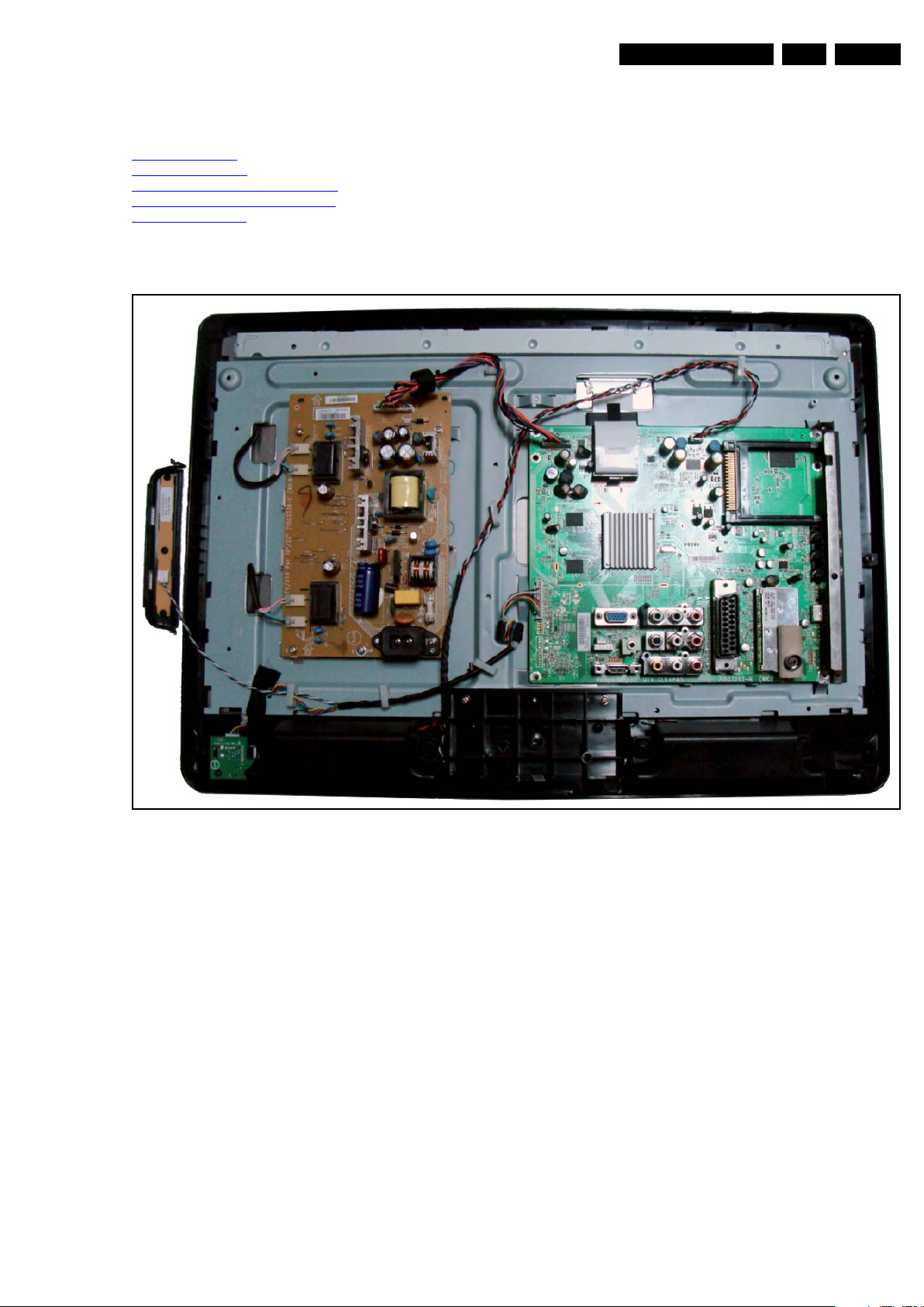
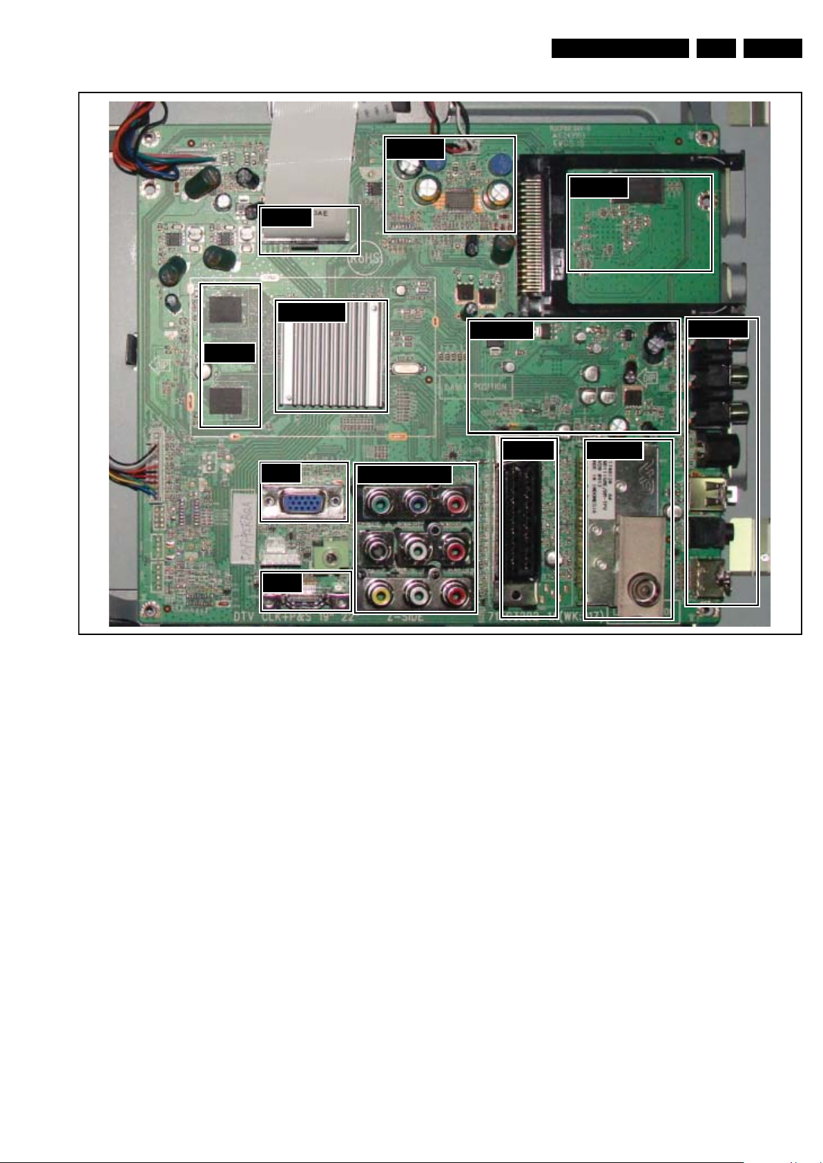
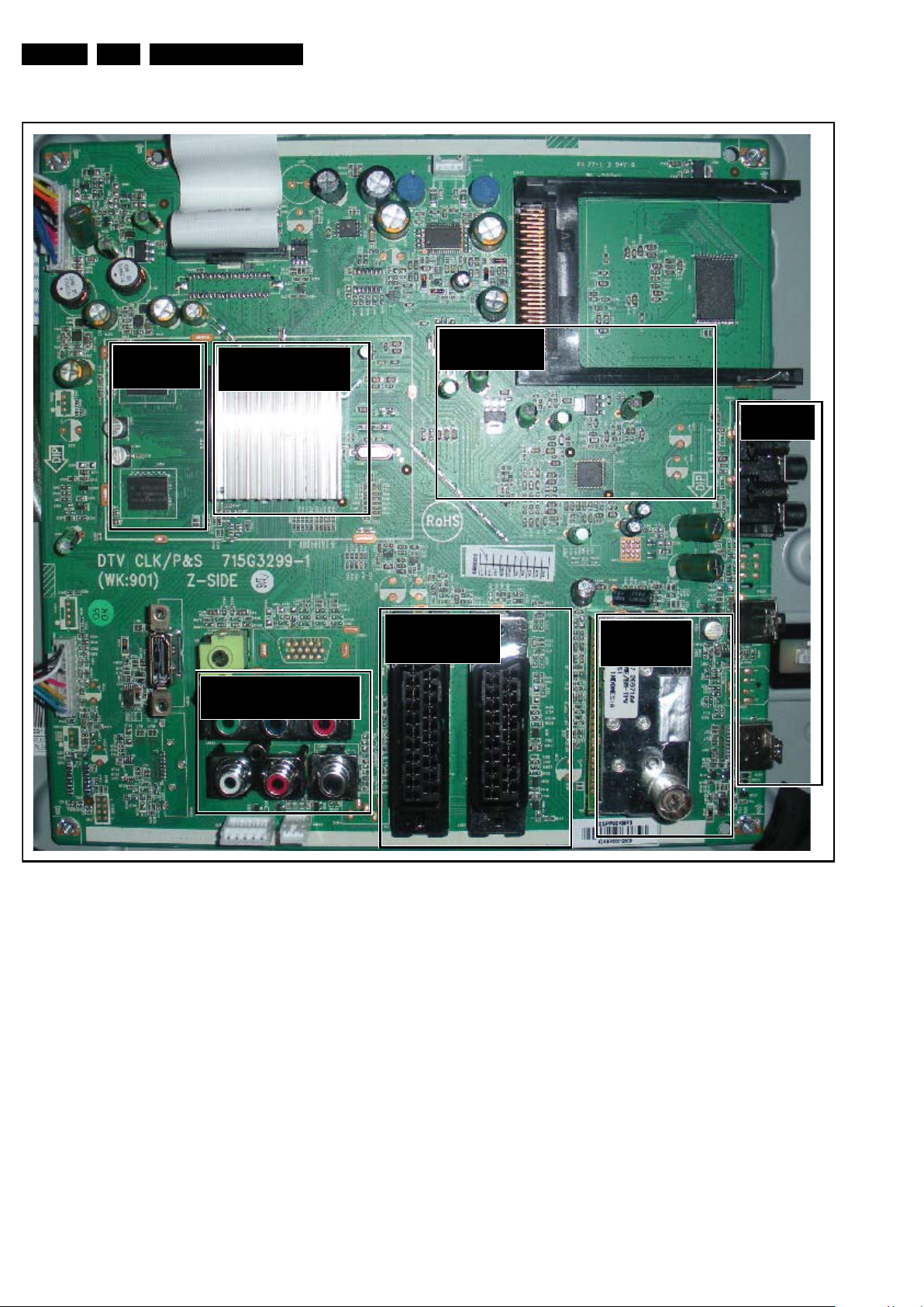
7.1.2 SSB Cell Layout
Circuit Descriptions
Figure 7-3 SSB top view 19" and 22" Click
2010-Jun-18
Circuit Descriptions
18291_200_090609.eps
100106
DDR
MT5362
Component
SCART
Tuner
AV I/O
FFC
Flash
DC-DC
Class-D
VGA
HDMI
EN 27TPM2.1E LA 7.
Figure 7-4 SSB top view 22PFL5604D/12
2010-Jun-18
EN 28 TPM2.1E LA7.
18290_205_090403.eps
100106
SCART
Tuner
Component
MT5362
DDR
DC-DC
AV I/O
Circuit Descriptions
Figure 7-5 SSB top view 26", 32" and 42"
2010-Jun-18
Circuit Descriptions
18290_206_090227.eps
100106
+18V
STB_PWR5V
+24V
TDA8932
Audio-Digital AMP
Q150 SI5441
CMOS
U155
TPS54231DR
BUCK
LC Circuit
U152 AME8810
Regulator
U151 LD1117
800mA Regulator
PANEL_VCC_ON/OFF
DV33 to DV18_CI
Q104 SI5441
CMOS
PANEL VCC(18V)
AV33
+5V_STB
DV18_DDR
Only for 0.3W stand by
Main Chip
DC to DC
Audio
PANEL
PANEL 5V(5V)
DV33SB
+5V_SW
Q105 SI4835
CMOS
OPWRSW
+18V_A
STAND BY
U103 L5947TR
Buck
DV11
U104 L5945TR
Buck
U158 LD1117
800mA Regulator
U153 LD1117
800mA Regulator
U154 LD1117
800mA Regulator
AV25 AV12
+5V_TUNER
U159 LD3908
800mA Regulator
1.4A
1.1A
0.25A
0.05A
MT5362
MT8295
5.3V
18293_200_100106.eps
100106
+12V
STB_PWR5V
+24V
TDA8932
Audio-Digital AM
P
Q150 SI5441
CMOS
U155 SC4525
BUCK
LC Circuit
U152 A
ME8810
Regulator
U151 LD1117
800mA Regulator
PANEL_VCC_ON/OFF
DV33
Q104 SI5441
CMOS
PANEL VCC(12V)
AV33
+5V_STB
DV18_DDR
Only for 0.
3W stand b
y
PANEL
PANEL 5V(5V)
DV33SB
+5V_SW
Q103 SI3441
FET
OPWRSW
+5V1_TUN
STAND BY
U103 L5945A
Buck
DV11
U
104 L5945A
Buck
U
156 LD1117
800mA Regulator
U
158
LD
1117
800mA Regulator
DV18_CI
U153 LD1117
800mA Regulato
r
U154 LD1117
800mA Regulator
AV25
AV12
+5V_TUNER
U159 LD3908
800mA Regulator
1.4A
1.1A
0.25A
0.05A
0.27
A(CMO L11)
0.28A(LPL WX2)
MT5362
MT8295
5.3V
Main Chip
DC to DC
Audio
EN 29TPM2.1E LA 7.
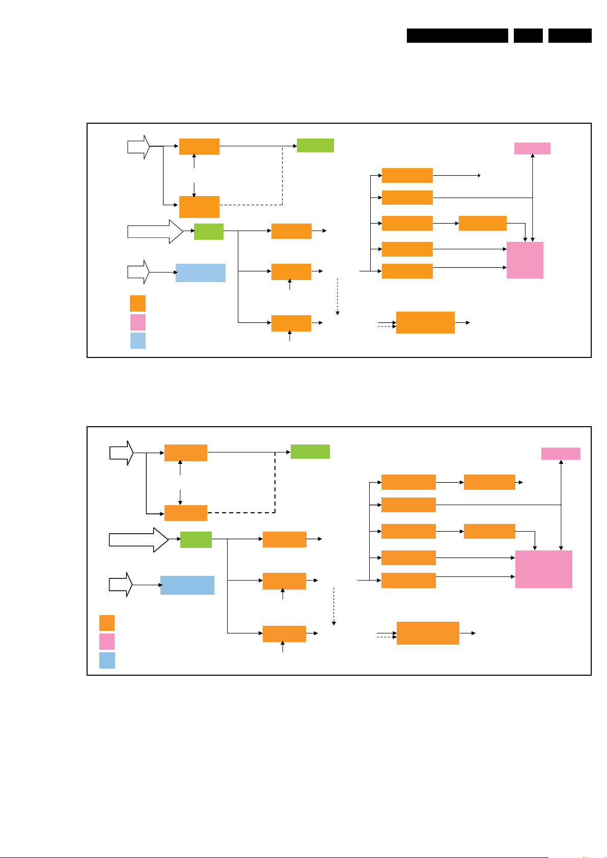
7.2 Main Supply
All Power Supply Units deliver the following voltages to the
chassis:
• +18V for panel, AMP, SW
• + 5V for USB, SW, STBY, TUNER
• +3.3 V for SD RAM, MST9A885GL, STMPS2171STR,
HDMI SWITCH, SW
• +2.6 V for DDR, MST9A885GL
Figure 7-6 Power Diagram 715G3292.
Figure 7-7 Power Diagram 715G3299.
2010-Jun-18

EN 30 TPM2.1E LA7.
Circuit Descriptions
7.3 MT5362BMG/B & MT5362ANG/B
7.3.1 Introduction
The MediaTek MT5362BMG/B & MT5362ANG/B family is a
back-end decoder and a TV controller and offers high
integration for advanced applications. It combines a transport
de-multiplexer, a high definition video decoder, an AC3 audio
decoder, a dual-link LVDS transmitter, and an
NTSC/PAL/SECAM TV decoder with a 3D comb filter
(NTSC/PAL). The MT5362BMG/B enables consumer
electronics manufactures to build high quality, low cost and
feature-rich DTV.
The MT5362BMG/B supports most Full-HD video decoder
standards, including H.264 (only for MT5362ANG/B), MPEG4,
MPEG2 and JPEG. The MT5362BMG/B also supports
MediaTek MDDITM de-interlace solution can reach very
smooth picture quality for motions. A 3D comb filter added to
the TV decoder recovers great details for still pictures. The
special colour processing technology provides natural, deep
colours and true studio quality video. Also, the MT5362BMG/B
family has built-in high resolution and high-quality audio codec.
Rich Features for High Value Products: The MT5362BMG/B
family enables true single chip experience. It integrates highquality HDMI1.3, high speed VGA ADC, dual-channel LVDS,
USB2.0 receiver and multi-media decoder
7.3.2 Function Description
Host CPU
• ARM926EJS
• 16K I-Cache and 16K D-Cache
• 8KB Instruction TCM
• JTAG ICE interface
• Watch Dog timers
• Build-in CPI analyser and Cache Hit Rate Meter
Transport Demultiplexer
• New generation 2 demultiplexer design
• Support a serial or parallel transport stream input
• Support ATSC, DVB, MPEG2 transport stream input
• Support DES/ 3-DES /DVB / AES de-scramblers
• Up to 8 PIDs even/odd keys for descrambling
• Support 32 PID filters and 32 table_id filters
• Support micro-processor table_id filtering
• Support hardware CRC-32 check
• Support PCR recovery function
• Supports a micro-processor for stream process and MEPG
start code detection
• Support DVB CA
• Supports simple trick play (playback / Pause / Fast
Forward (upto ×32) through USB or Flash
• Point, horizontal/Vertical line primitive drawings
• Rectangle fill and gradient fill functions
• bit with transparent options
• Alpha blending and alpha composition bit
• Stretch bit
• Font rendering by colour expansion
• YCbCr to RGB colour space conversion
Image Resizer
• Supports 2, 4, and 8 bpp index format, 16 bpp/32 bpp
direct colour format
• Supports 420/422 video format
• Supports 420/422/444 JPEG format
• Arbitrary ratio vertical /horizontal scaling of video, from
1/128X to 128X
• Simple DMA
OSD Plane
• Two linking list OSDs with multiple colour mode and one of
them has scaler
Video Plane
• Supports video capture and over scan
• Flesh tone management
• Gamma correction
• Colour Transient Improvement (CTI)
•2D Peaking
• Saturation / hue adjustment
• Brightness and contrast adjustment
• Black and White level extender
• Adaptive Luma/Chroma management
• Automatic detect film or video source
• 3:2/2:2 pull down source detection
• Supports maximum 1920 width motion-adaptive deinterlace
• Supports maximum 1920 width motion-adaptive deinterlace
• Supports excellent low angle image processing
• Arbitrary ratio vertical/ horizontal scaling of video, from
1/32X to 32X
• Advanced non-linear panorama scaling
• Programmable zoom viewer
• Progressive scan output
• Supports alpha blending
• Dithering processing for flat panel display
• Frame rate conversion
• Supports FHD panel and VGA dot-to-dot
• Supports PIP/POP, (dual de-interlace, one HD and one
SD)
LVDS
• Supports 6/8/10-bit single-channel or dual-channel LVDS
transmitter, 2-link LVDS up-to 175MHz
• Built-in spread spectrum for EMI performance
• Programmable panel timing output
MPEG 2 Decoder
• MEPG MP@ML, MP@HL and MPEG-1 video standards
• Supports de-blocking filter
MPEG 1 Decoder
MPEG 4.2 Decoder
• ASP@15 (720P)
H.264 (MPEG4.10) HD Decoder (AVC)
• MP@L4.1, BP@L3 (baseline) video standard
Still image decoding
• JPEG (base-line or progressive)
2D Graphics
• Support multiple colour modes
2010-Jun-18
CVBS In
• On-chip 54MHz 10Bit video ADC
• Supports PAL (B, G, D, H, M, N, I, Nc), NTSC-4.43,
SECAM
• NTSC/PAL supports 3D/2D comb filter
• Built-in motion-adaptive 3D Noise Reduction
• VBI data slicer for CC/TT decoding
• Supports 2-S-Video
• Max. Supports 4-channel CVBS
• Supports SCART connector
Component Video In
• Supports two component video inputs
• Supports 480i/480p/576i/576p/720p/1080i/1080p
Audio ADC
• 2 channel on chip Audio ADC
 Loading...