

PHILIPS 26PF9531/10, 26PF9631D/10, 32PF9541/10, 32PF9551/10, 32PF9631D/79 Service manual & schematics
...
Published by EL 0670 BG CD Customer Service Printed in the Netherlands Subject to modification EN 3122 785 15952
©
Copyright 2006 Philips Consumer Electronics B.V. Eindhoven, The Netherlands.
All rights reserved. No part of this publication may be reproduced, stored in a
retrieval system or transmitted, in any form or by any means, electronic,
mechanical, photocopying, or otherwise without the prior permission of Philips.
Colour Television Chassis
BJ3.0E
LA
ME5P
SOFTWRAP 2k5
(STEP 2k4)
STEP 2k6
G_15951_000.eps
050906
EDGE
(ENTRY+)
Contents Page Contents Page
1. Technical Specifications, Connections, and Chassis
Overview 2
2. Safety Instructions, Warnings, and Notes 7
3. Directions for Use 9
4. Mechanical Instructions 10
5. Service Modes, Error Codes, and Fault Finding 17
6.
Block Diagrams, Test Point Overviews, and
Waveforms
Wiring Diagram 26” ME5P 49
Wiring Diagram 32” Soft Wrap 2k5 50
Wiring Diagram 32” Step 2k4 51
Wiring Diagram 32” Step 2k6 52
Wiring Diagram 37” 2k6 53
Wiring Diagram 42” Edge 54
Block Diagram Display Supply 26” 55
Block Diagram Display Supply 32” 56
Block Diagram Display/Platform Supply 37” 57
Block Diagram Display Supply 42” 58
Block Diagram Video 59
Block Diagram Audio 60
Block Diagram Control & Clock Signals 61
Test Points SSB Top and Bottom Side 62-67
I2C Overview 68
Supply Lines Overview 69
7.
Circuit Diagrams and PWB Layouts Drawing PWB
Display Supply 32”: Filter & Stby (A1) 70 73-76
Display Supply 32”: Supply (A2) 71 73-76
Display Supply 32”: Connections (A3) 72 73-76
Display Supply 37”: Part 1 (A1) 77 82-87
Display Supply 37”: Part 2 (A2) 78 82-87
Platform Supply 37”: Auxiliary Supply (A3) 79 82-87
Platform Supply 37”: Standby Supply (A4) 80 82-87
Platform Supply 37”: 25W Supply (A5) 81 82-87
Display Supply 42”: Mains Filter & Stby A (A1) 88 92-97
Display Supply 42”: Part A (A2) 89 92-97
Display Supply 42”: Mains Filter & Stby B (A3) 90 92-97
Display Supply 42”: Part B (A4) 91 92-97
Display Supply 26”: Mains Filter & Stby (AC1) 98 103-107
Display Supply 26”: Supply (AC2) 99 103-107
Display Supply 26”: Standby (AC3) 100 103-107
Display Supply 26”: Audio Left / Right (AC4) 101 103-107
Display Supply 26”: Protection/Mute Cntrl(AC5) 102 103-107
Ambi Light Step 2k6 (AL1) 108 111
Ambi Light Step 2k6 (AL2) 109 111
Ambi Light Step 2k6 (AL3) 110 111
Small Signal Board (B1-B12) 129-167 170-175
Externals: A (BE1) 176 179
Externals: B (BE2) 177 179
Externals: C (BE3) 178 179
Audio Panel (37”): Left / Right (C1) 180 182
Audio Panel (37”): Protection & Mute Ctrl (C2) 181 182
Side I/O Panel (26”) Rear Facing (D) 183 184
Side I/O Panel (D) 185 186
Control Board (26”) (E) 187 188
Control Board (32”) (E) 189 189
Control Board (37”) (E) 190 190
Control Board (42”) (E) 191 191
Front IR / LED Panel (26”) (J) 192 192
LED Panel (32”) (J) 193 194
LED Panel (37”) (J) 195 196
LED Panel (42”) (J) 197 198
Standby & Audio Panel (32”) (SA1-SA5) 199-203 204-206
Standby & Audio Panel (42”) (SA1-SA3) 207-209 210-212
8. Alignments 213
9. Circuit Descriptions, Abbreviation List, and IC Data
Sheets 220
10. Spare Parts List 243
11. Revision List 263

EN 2 BJ3.0E LA1.
Technical Specifications, Connections, and Chassis Overview
1. Technical Specifications, Connections, and Chassis Overview
Index of this chapter:
1.1 Technical Specifications
1.2 Connection Overview
1.3 Chassis Overview
Notes:
• Data below can deviate slightly from the actual situation,
due to the different set executions
• Specifications are indicative (subject to change).
1.1 Technical Specifications
1.1.1 Vision
Display type : LCD
Screen size : 26” (66 cm), 16:9
Resolution (HxV pixels) : 1366x768p
Typ. contrast ratio : 3500:1 (26”)
Min. light output (cd/m
Viewing angle (HxV degrees) : 176x176
Tuning system : PLL
TV Colour systems : PAL
Video playback : PAL
Cable : Unscrambled digital
Tuner bands : VHF
Supported video formats : 640x480i - 1fH
Supported computer formats : 640x480 @ 60Hz
2
) : 500 (26 and 37”)
: 32” (82 cm), 16:9
: 37” (94 cm), 16:9
: 42” (107 cm), 16:9
: 6000:1 (32 & 37”)
: 4000:1 (42”)
: 550 (32 and 42”)
: SECAM (not for 32”)
: DVB-T (only for digital
sets)
: SECAM
: NTSC
cable - QAM
: Digital cable ready -
Common Interface
(only for digital sets)
: UHF
: S-band
: Hyper-band
: 640x480p - 2fH
: 720x576i - 1fH
: 720x576p - 2fH
: 1280x720p - 3fH
: 1920x1080i - 2fH
: 800x600 @ 60Hz
: 1024x768 @ 60Hz
: 1366x768 @ 60Hz
1.1.3 Miscellaneous
Power supply:
- Mains voltage (VAC) : 220 - 240
- Mains frequency (Hz) : 50/60 Hz
Ambient conditions:
- Temperature range (qC) : +5 to +40
- Maximum humidity : 90% R.H.
Power consumption (values are indicative)
- Normal operation (W) : | 130 (26”)
: | 79/128 (32”)
: | 163 (37 & 42”)
- Standby (W) : < 2
Dimensions (WxHxD in cm) : 69.8x49.5x10.4 (26”)
: 87.5x61.0x10.7 (32”)
: 99.1x70.7x11.4 (37”)
: 123.7x68.8x11.0 (42”)
Weight (kg/lbs) : 16 / 35.2 (26”)
: 22 / 48.4 (32”)
: 26 / 57.2 (37”)
: 31.5 / 69.3 (42”)
1.1.2 Sound
Sound systems : AV Stereo
Maximum power (W
) : 2 x 8 (26 and 32”)
RMS
: FM/FM (5.5-5.74)
(B/G)
: NICAM B/G (5.5-5.85)
: NICAM D/K
(6.5.-5.85) (Hung)
: NICAM I (6.0-6.52)
: 2 x 15 (32, 37 and 42”)
Technical Specifications, Connections, and Chassis Overview
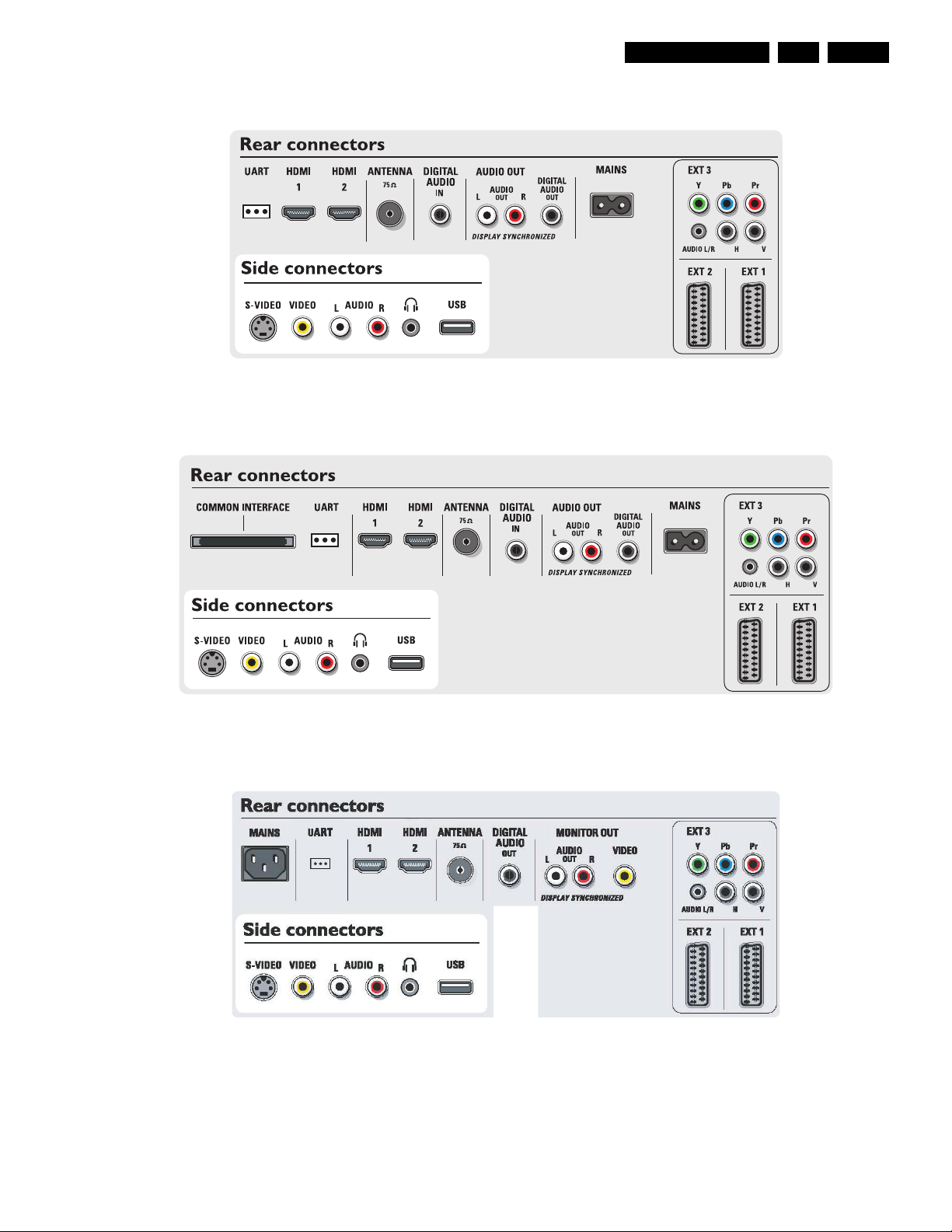
1.2 Connection Overview
Figure 1-1 Side and rear I/O connections analogue sets
G_15950_039.eps
060406
EN 3BJ3.0E LA 1.
Figure 1-2 Side and rear I/O connections digital sets
Figure 1-3 Side and rear I/O connections 32PF9541/10 & 32PF9641D/10
G_15950_040.eps
G_15951_004.eps
010906
060406

Technical Specifications, Connections, and Chassis Overview
EN 4 BJ3.0E LA1.
Note: The following connector colour abbreviations are used
(acc. to DIN/IEC 757): Bk= Black, Bu= Blue, Gn= Green, Gy=
Grey, Rd= Red, Wh= White, and Ye= Yellow.
1.2.1 Side Connections
S-Video (Hosiden): Video Y/C - In
1 -Ground Y Gnd H
2 -Ground C Gnd H
3 -Video Y 1 V
PP
/ 75 ohm j
4 -Video C 0.3 VPPP / 75 ohm j
Cinch: Video CVBS - In, Audio - In
Ye - Video CVBS 1 VPP / 75 ohm jq
Wh - Audio L 0.5 V
RMS
/ 10 kohm jq
Rd - Audio R 0.5 V
RMS
/ 10 kohm jq
Headphone - Out
Bk - Headphone 32 - 600 ohm / 10 mW ot
USB2.0
Figure 1-4 USB (type A)
1 -+5V k
2 -Data (-) jk
3 -Data (+) jk
4 -Ground Gnd H
1.2.2 Rear Connections
Common Interface
68p - See diagram B10A jk
Service Connector (UART)
1 -UART_TX Transmit k
2 -Ground Gnd H
3 -UART_RX Receive j
HDMI 1 & 2: Digital Video, Digital Audio - In
Figure 1-5 HDMI (type A) connector
1 -D2+ Data channel j
2 -Shield Gnd H
3 -D2- Data channel j
4 -D1+ Data channel j
5 -Shield Gnd H
6 -D1- Data channel j
7 -D0+ Data channel j
8 -Shield Gnd H
9 -D0- Data channel j
10 - CLK+ Data channel j
11 - Shield Gnd H
12 - CLK- Data channel j
13 - n.c.
14 - n.c.
15 - DDC_SCL DDC clock j
16 - DDC_SDA DDC data jk
17 - Ground Gnd H
18 - +5V j
19 - HPD Hot Plug Detect j
20 - Ground Gnd H
Aerial - In
- - IEC-type (EU) Coax, 75 ohm D
DIGITAL AUDIO Cinch: S/PDIF - In
Bk - Coaxial 0.2 - 0.6V
PP
/ 75 ohm jq
AUDIO OUT Cinch: Audio - Out
Wh - Audio L 0.5 V
RMS
/10 kohm kq
Rd - Audio R 0.5 V
RMS
/ 10 kohm kq
DIGITAL AUDIO Cinch: S/PDIF - Out
Bk - Coaxial 0.2 - 0.6VPP / 75 ohm kq
Monitor Out: Cinch: Audio - Out
Wh - Audio L 0.5 V
RMS
/10 kohm kq
Rd - Audio R 0.5 V
RMS
/ 10 kohm kq
Monitor Out: Video CVBS - Out
Ye - Video CVBS 1 VPP / 75 ohm kq
EXT1: Video RGB/YC - In, CVBS - In/Out, Audio - In/Out
Figure 1-6 SCART connector
1 -Audio R 0.5 V
RMS
/ 1 kohm k
2 -Audio R 0.5 V
RMS
/ 10 kohm j
3 -Audio L 0.5 V
RMS
/ 1 kohm k
4 -Ground Audio Gnd H
5 -Ground Blue Gnd H
6 -Audio L 0.5 V
RMS
/ 10 kohm j
7 -Video Blue/C-out 0.7 VPP / 75 ohm jk
8 -Function Select 0 - 2 V: INT
4.5 - 7 V: EXT 16:9
9.5 - 12 V: EXT 4:3 j
9 -Ground Green Gnd H
10 - n.c.
11 - Video Green 0.7 V
PP
/ 75 ohm j
12 - n.c.
13 - Ground Red Gnd H
14 - Ground P50 Gnd H
15 - Video Red/C 0.7 V
PP
/ 75 ohm j
16 - Status/FBL 0 - 0.4 V: INT
1 - 3 V: EXT / 75 ohm j
17 - Ground Video Gnd H
18 - Ground FBL Gnd H
19 - Video CVBS/Y 1 V
PP
/ 75 ohm k
20 - Video CVBS/Y 1 VPP / 75 ohm j
21 - Shield Gnd H
EXT2: Video RGB/YC - In, CVBS - In/Out, Audio - In/Out
Figure 1-7 SCART connector
1 -Audio R 0.5 V
RMS
/ 1 kohm k
2 -Audio R 0.5 V
RMS
/ 10 kohm j
3 -Audio L 0.5 V
RMS
/ 1 kohm k
4 -Ground Audio Gnd H
1 2 3 4
E_06532_022.eps
300904
19
1
18 2
E_06532_017.eps
250505
21
20
1
2
E_06532_001.eps
050404
21
20
1
2
E_06532_001.eps
050404

Technical Specifications, Connections, and Chassis Overview
LCD SUPPLY/STANDBY/
AUDIO PANEL
AC
CONTROL BOARD
SIDE I/O PANEL
E
SMALL SIGNAL BOARD
B
D
EXTERNAL I/O PANEL
BE
LED PANEL
J
G_15951_002.eps
140806
G_15951_013.eps
010906
AL
B
E
J
AMBI LIGHT PANEL
SA
STANDBY &
AUDIO PANEL
AL
AMBI LIGHT PANEL
A
SUPPLY PANEL
BE
EXTERNAL I/O
PANEL
D
SIDE I/O PANEL
CONTROL BOARD
SMALL SIGNAL
BOARD
LED PANEL
EN 5BJ3.0E LA 1.
5 -Ground Blue Gnd H
6 -Audio L 0.5 V
7 -Video Blue/C-out 0.7 VPP / 75 ohm jk
8 -Function Select 0 - 2 V: INT
9 -Ground Green Gnd H
10 - Easylink P50 0 - 5 V / 4.7 kohm jk
11 - Video Green 0.7 V
12 - n.c.
13 - Ground Red Gnd H
14 - Ground Data Gnd H
15 - Video Red/C 0.7 V
16 - Status/FBL 0 - 0.4 V: INT
17 - Ground Video Gnd H
1.3 Chassis Overview
/ 10 kohm j
RMS
4.5 - 7 V: EXT 16:9
9.5 - 12 V: EXT 4:3 j
/ 75 ohm j
PP
/ 75 ohm j
PP
1 - 3 V: EXT / 75 ohm j
18 - Ground FBL Gnd H
19 - Video CVBS/Y 1 V
20 - Video CVBS/Y 1 VPP / 75 ohm j
21 - Shield Gnd H
EXT3: Cinch: Video YPbPrHV- In
Gn - Video Y 1 V
Bu - Video Pb 0.7 VPP / 75 ohm jq
Rd - Video Pr 0.7 VPP / 75 ohm jq
Bk - H-sync 0 - 5 V jq
Bk - V-sync 0 - 5 V jq
EXT3: Mini Jack: Audio - In
Rd - Audio R 0.5 V
Wh - Audio L 0.5 V
/ 75 ohm k
PP
/ 75 ohm jq
PP
/ 10 kohm j
RMS
/ 10 kohm j
RMS
Figure 1-8 PWB/CBA locations (26-inch model)
Figure 1-9 PWB/CBA locations (32-inch model)

EN 6 BJ3.0E LA1.
G_15950_041.eps
070406
AL
B
E
J
AMBI LIGHT PANEL
C
AUDIO PANEL
AL
AMBI LIGHT PANEL
A
SUPPLY PANEL
( AC for 26” models)
BE
EXTERNAL I/O
PANEL
D
SIDE I/O PANEL
CONTROL BOARD
SMALL SIGNAL
BOARD
LED PANEL
Technical Specifications, Connections, and Chassis Overview
Figure 1-10 PWB/CBA locations (37-inch model)

Safety Instructions, Warnings, and Notes
2. Safety Instructions, Warnings, and Notes
EN 7BJ3.0E LA 2.
Index of this chapter:
2.1 Safety Instructions
2.2 Warnings
2.3 Notes
2.1 Safety Instructions
Safety regulations require the following during a repair:
• Connect the set to the Mains/AC Power via an isolation
transformer (> 800 VA).
• Replace safety components, indicated by the symbol h,
only by components identical to the original ones. Any
other component substitution (other than original type) may
increase risk of fire or electrical shock hazard.
Safety regulations require that after a repair, the set must be
returned in its original condition. Pay in particular attention to
the following points:
• Route the wire trees correctly and fix them with the
mounted cable clamps.
• Check the insulation of the Mains/AC Power lead for
external damage.
• Check the strain relief of the Mains/AC Power cord for
proper function.
• Check the electrical DC resistance between the Mains/AC
Power plug and the secondary side (only for sets that have
a Mains/AC Power isolated power supply):
1. Unplug the Mains/AC Power cord and connect a wire
between the two pins of the Mains/AC Power plug.
2. Set the Mains/AC Power switch to the "on" position
(keep the Mains/AC Power cord unplugged!).
3. Measure the resistance value between the pins of the
Mains/AC Power plug and the metal shielding of the
tuner or the aerial connection on the set. The reading
should be between 4.5 Mohm and 12 Mohm.
4. Switch "off" the set, and remove the wire between the
two pins of the Mains/AC Power plug.
• Check the cabinet for defects, to prevent touching of any
inner parts by the customer.
2.2 Warnings
• All ICs and many other semiconductors are susceptible to
electrostatic discharges (ESD w). Careless handling
during repair can reduce life drastically. Make sure that,
during repair, you are connected with the same potential as
the mass of the set by a wristband with resistance. Keep
components and tools also at this same potential. Available
ESD protection equipment:
– Complete kit ESD3 (small tablemat, wristband,
connection box, extension cable and earth cable) 4822
310 10671.
– Wristband tester 4822 344 13999.
• Be careful during measurements in the high voltage
section.
• Never replace modules or other components while the unit
is switched "on".
• When you align the set, use plastic rather than metal tools.
This will prevent any short circuits and the danger of a
circuit becoming unstable.
2.3 Notes
2.3.1 General
• Measure the voltages and waveforms with regard to the
chassis (= tuner) ground (H), or hot ground (I), depending
on the tested area of circuitry. The voltages and waveforms
shown in the diagrams are indicative. Measure them in the
Service Default Mode (see chapter 5) with a colour bar
signal and stereo sound (L: 3 kHz, R: 1 kHz unless stated
otherwise) and picture carrier at 475.25 MHz for PAL, or
61.25 MHz for NTSC (channel 3).
• Where necessary, measure the waveforms and voltages
with (D) and without (E) aerial signal. Measure the
voltages in the power supply section both in normal
operation (G) and in stand-by (F). These values are
indicated by means of the appropriate symbols.
• The semiconductors indicated in the circuit diagram and in
the parts lists, are interchangeable per position with the
semiconductors in the unit, irrespective of the type
indication on these semiconductors.
• Manufactured under license from Dolby Laboratories.
“Dolby”, “Pro Logic” and the “double-D symbol”, are
trademarks of Dolby Laboratories.
2.3.2 Schematic Notes
• All resistor values are in ohms, and the value multiplier is
often used to indicate the decimal point location (e.g. 2K2
indicates 2.2 kohm).
• Resistor values with no multiplier may be indicated with
either an "E" or an "R" (e.g. 220E or 220R indicates 220
ohm).
• All capacitor values are given in micro-farads (P x10
nano-farads (n= x10-9), or pico-farads (p= x10
• Capacitor values may also use the value multiplier as the
decimal point indication (e.g. 2p2 indicates 2.2 pF).
• An "asterisk" (*) indicates component usage varies. Refer
to the diversity tables for the correct values.
• The correct component values are listed in the Spare Parts
List. Therefore, always check this list when there is any
doubt.
2.3.3 Rework on BGA (Ball Grid Array) ICs
General
Although (LF)BGA assembly yields are very high, there may
still be a requirement for component rework. By rework, we
mean the process of removing the component from the PWB
and replacing it with a new component. If an (LF)BGA is
removed from a PWB, the solder balls of the component are
deformed drastically so the removed (LF)BGA has to be
discarded.
Device Removal
As is the case with any component that, is being removed, it is
essential when removing an (LF)BGA, that the board, tracks,
solder lands, or surrounding components are not damaged. To
remove an (LF)BGA, the board must be uniformly heated to a
temperature close to the reflow soldering temperature. A
uniform temperature reduces the risk of warping the PWB.
To do this, we recommend that the board is heated until it is
certain that all the joints are molten. Then carefully pull the
component off the board with a vacuum nozzle. For the
appropriate temperature profiles, see the IC data sheet.
Area Preparation
When the component has been removed, the vacant IC area
must be cleaned before replacing the (LF)BGA.
Removing an IC often leaves varying amounts of solder on the
mounting lands. This excessive solder can be removed with
either a solder sucker or solder wick. The remaining flux can be
removed with a brush and cleaning agent.
After the board is properly cleaned and inspected, apply flux on
the solder lands and on the connection balls of the (LF)BGA.
Note: Do not apply solder paste, as this has been shown to
result in problems during re-soldering.
-6
),
-12
).

EN 8 BJ3.0E LA2.
P
b
Safety Instructions, Warnings, and Notes
Device Replacement
The last step in the repair process is to solder the new
component on the board. Ideally, the (LF)BGA should be
aligned under a microscope or magnifying glass. If this is not
possible, try to align the (LF)BGA with any board markers.
So as not to damage neighbouring components, it may be
necessary to reduce some temperatures and times.
More Information
For more information on how to handle BGA devices, visit this
URL: www.atyourservice.ce.philips.com (needs subscription,
not available for all regions). After login, select “Magazine”,
then go to “Repair downloads”. Here you will find Information
on how to deal with BGA-ICs.
2.3.4 Lead-free Solder
Philips CE is producing lead-free sets (PBF) from 1.1.2005
onwards.
Identification: The bottom line of a type plate gives a 14-digit
serial number. Digits 5 and 6 refer to the production year, digits
7 and 8 refer to production week (in example below it is 1991
week 18).
MODEL :
PROD.NO:
32PF9968/10
AG 1A0617 000001
220-240V 50/60Hz
VHF+S+H+UHF
S
MADE IN BELGIUM
~
128W
BJ3.0E LA
E_06532_024.eps
130606
avoid mixed regimes. If this cannot be avoided, carefully
clear the solder-joint from old tin and re-solder with new tin.
• Use only original spare-parts listed in the Service-Manuals.
Not listed standard material (commodities) has to be
purchased at external companies.
• Special information for lead-free BGA ICs: these ICs will be
delivered in so-called "dry-packaging" to protect the IC
against moisture. This packaging may only be opened
shortly before it is used (soldered). Otherwise the body of
the IC gets "wet" inside and during the heating time the
structure of the IC will be destroyed due to high (steam-)
pressure inside the body. If the packaging was opened
before usage, the IC has to be heated up for some hours
(around 90°C) for drying (think of ESD-protection!).
Do not re-use BGAs at all!
• For sets produced before 1.1.2005, containing leaded
soldering tin and components, all needed spare parts will
be available till the end of the service period. For the repair
of such sets nothing changes.
In case of doubt whether the board is lead-free or not (or with
mixed technologies), you can use the following method:
• Always use the highest temperature to solder, when using
SAC305 (see also instructions below).
• De-solder thoroughly (clean solder joints to avoid mix of
two alloys).
Caution:
profile, which is coupled to the 12NC. For an overview of these
profiles, visit the website
(needs subscription, but is not available for all regions)
You will find this and more technical information within the
"Magazine", chapter "Repair downloads".
For additional questions please contact your local repair help
desk.
For BGA-ICs, you must use the correct temperature-
www.atyourservice.ce.philips.com
Figure 2-1 Serial number example
Regardless of the special lead-free logo (which is not always
indicated), one must treat all sets from this date onwards
according to the rules as described below.
Figure 2-2 Lead-free logo
Due to lead-free technology some rules have to be respected
by the workshop during a repair:
• Use only lead-free soldering tin Philips SAC305 with order
code 0622 149 00106. If lead-free solder paste is required,
please contact the manufacturer of your soldering
equipment. In general, use of solder paste within
workshops should be avoided because paste is not easy to
store and to handle.
• Use only adequate solder tools applicable for lead-free
soldering tin. The solder tool must be able:
– To reach a solder-tip temperature of at least 400°C.
– To stabilise the adjusted temperature at the solder-tip.
– To exchange solder-tips for different applications.
• Adjust your solder tool so that a temperature of around
360°C - 380°C is reached and stabilised at the solder joint.
Heating time of the solder-joint should not exceed ~ 4 sec.
Avoid temperatures above 400°C, otherwise wear-out of
tips will increase drastically and flux-fluid will be destroyed.
To avoid wear-out of tips, switch “off” unused equipment or
reduce heat.
• Mix of lead-free soldering tin/parts with leaded soldering
tin/parts is possible but PHILIPS recommends strongly to
2.3.5 Alternative BOM identification
In September 2003, Philips CE introduced a change in the way
the serial number (or production number, see Figure 2-1) is
composed. From this date on, the third digit in the serial
number (example: AG2B0335000001) indicates the number of
the alternative BOM (Bill of Materials used for producing the
specific model of TV set). It is possible that the same TV model
on the market is produced with e.g. two different types of
displays, coming from two different O.E.M.s.
By looking at the third digit of the serial number, the service
technician can see if there is more than one type of B.O.M.
used in the production of the TV set he is working with. He can
then consult the At Your Service Web site, where he can type
in the Commercial Type Version Number of the TV set (e.g.
28PW9515/12), after which a screen will appear that gives
information about the number of alternative B.O.M.s used.
If the third digit of the serial number contains the number 1
(example: AG1B033500001), then there is only one B.O.M.
version of the TV set on the market. If the third digit is a 2
(example: AG2B0335000001), then there are two different
B.O.M.s.
the correct spare parts!
For the third digit, the numbers 1...9 and the characters A...Z
can be used, so in total: 9 plus 26 = 35 different B.O.M.s can
be indicated by the third digit of the serial number.
2.3.6 Practical Service Precautions
• It makes sense to avoid exposure to electrical shock.
• Always respect voltages. While some may not be
Information about this is important for ordering
While some sources are expected to have a possible
dangerous impact, others of quite high potential are of
limited current and are sometimes held in less regard.
dangerous in themselves, they can cause unexpected
reactions that are best avoided. Before reaching into a
powered TV set, it is best to test the high voltage insulation.
It is easy to do, and is a good service precaution.

3. Directions for Use
You can download this information from the following websites:
http://www.philips.com/support
http://www.p4c.philips.com
Directions for Use
EN 9BJ3.0E LA 3.
EN 10 BJ3.0E LA4.
G_15951_003.eps
140806
G_15951_014.eps
010906
Mechanical Instructions
4. Mechanical Instructions
Index of this chapter:
4.1 Cable Dressing
4.2 Service Positions
4.3 Assy/Panel Removal
4.4 Set Re-assembly
4.1 Cable Dressing
Notes:
• Figures below can deviate slightly from the actual situation,
due to the different set executions.
• Follow the disassemble instructions in described order.
They apply to the 37” sets, unless stated otherwise.
Figure 4-1 Cable dressing (26-inch model)
Figure 4-2 Cable dressing (32-inch model)
Mechanical Instructions
EN 11BJ3.0E LA 4.
Figure 4-3 Cable dressing (37-inch model)
4
.2 Service Positions
For easy servicing of this set, there are a few possibilities
created:
• The buffers from the packaging.
• Foam bars (created for service).
• Aluminium service stands (created for Service).
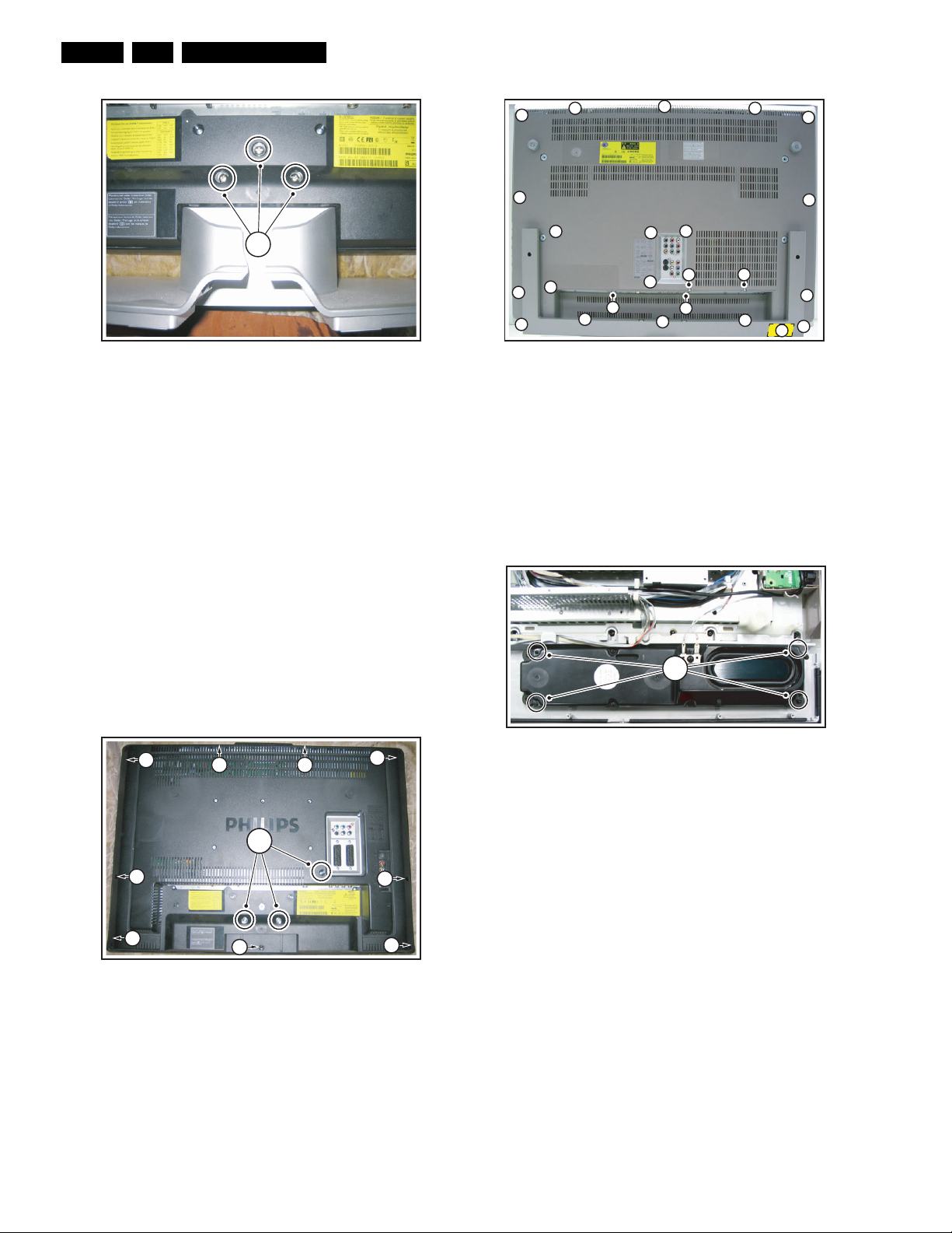
4.2.1 Foam Bars
Figure 4-4 Foam bars
The foam bars (order code 3122 785 90580 for two pieces) can
be used for all types and sizes of Flat TVs. By laying the TV
face down on the (ESD protective) foam bars, a stable situation
is created to perform measurements and alignments.
By placing a mirror under the TV, you can monitor the screen.
4.2.2 Aluminium Stands
Figure 4-5 Aluminium stands (drawing of MkI)
The new MkII aluminium stands (not on drawing) with order
code 3122 785 90690, can also be used to do measurements,
alignments, and duration tests. The stands can be
(dis)mounted quick and easy by means of sliding them in/out
the "mushrooms". The new stands are backwards compatible
with the earlier models.
Important: For (older) FTV sets without these "mushrooms", it
is obligatory to use the provided screws, otherwise it is possible
to damage the monitor inside!
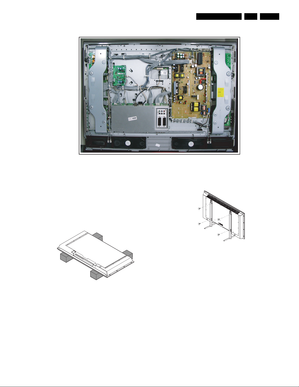
4.3 Assy/Panel Removal
4.3.1 Stand removal (26” sets)
The stand can be removed after removing the screws [1]. See
figure “Stand Removal 26” sets” for details.
G_15950_042.eps
060406
E_06532_018.eps
170504
E_06532_019.eps
170504
EN 12 BJ3.0E LA4.
G_15951_001.eps
010906
1
G_15951_005.eps
010906
2
2 2
2
2
2
2
2
2
2
G_15970_036.eps
200306
2
2
2
2
2
2
2
2
2
2
2
2
2
2
2
2
2
2
2
2
2
2
2
1
G_15960_111.eps
070306
1
Mechanical Instructions
Figure 4-6 Stand removal 26” sets
.3.2 Rear Cover
4
Disconnect the Mains/AC Power cord before you remove the
rear cover!
Note: at some sets a sticker containing the type number [1] has
been added on the right lower corner of the rear cover, allowing
the customer to read the number without lifting the set from the
wall.
1. Place the TV set upside down on a table top, using the
foam bars (see part “Foam Bars”).
Caution: do not put pressure on the display, but let the
monitor lean on the Front cover.
2. Remove the “mushrooms” from the Rear Cover.
3. Remove T10 tapping and parker screws [2] from the top,
centre, bottom, left and right side of the Rear Cover and
underneath the main I/O panel that hold the cover.
4. Lift the Rear Cover from the TV. Make sure that wires and
flat foils are not damaged while lifting the rear cover.
Figure 4-8 Rear Cover removal 37” sets
4.3.3 Speaker
After removing the rear cover, you gain access to the speakers.
Each speaker is fixed with four T10 screws [1]. See Figure
“Speaker removal”. After removal of these screws, the
speakers can be removed.
Caution: never disconnect the speakers with a playing set,
because otherwise the class-D audio amplifiers could be
damaged!
Figure 4-7 Rear Cover removal 26” sets
Figure 4-9 Speaker removal
4.3.4 AmbiLight Inverter Panel
There are two AmbiLight Inverter Panels used in this set.
Before they can be removed, the vertical brackets on the left
and right side that hold the “mushrooms” have to be removed.
Each one of them is fixed with four T10 tapping screws [1]. See
Figure “Right Vertical Bracket Removal” for instructions on how
to remove the brackets.
Mechanical Instructions
G_15970_038.eps
200306
1
1
G_15970_039.eps
200306
1
2
G_15960_099.eps
070306
11
G_15960_100.eps
070306
11
12
EN 13BJ3.0E LA 4.
4.3.5 Control Panel
The Control Panel can be taken out by removing the two T10
screws [1] that hold the plastic frame. See Figure “Control
panel removal”. The cable can not be disconnected from the
assy at this moment. While still connected to the assy, the
cable must now be released from the two clamps on the
chassis nearest to the assy.
Figure 4-10 Right Vertical Bracket removal
he instructions to remove the right AmbiLight Inverter Panel
T
(seen from the back side of the set) are as follows:
1. Disconnect the cables [1] from the panel.
2. Push back the clamps [2] on the right side that hold the
assy.
3. Take out the panel (it hinges on the left side).
When defective, replace the whole unit.
Figure 4-12 Control panel removal
The assy is packed into two plastic frames. To unpack the
inner frame, lift the two clamps [1] of the outer frame and take
the inner frame out. See Figure “Control panel frame removal”.
Figure 4-11 AmbiLight right side Inverter Panel removal
Figure 4-13 Control panel frame removal
To take the assy out of the inner frame, lift the two clamps of
the frame [2] and slightly pull the assy out. Only now the cable
can be disconnected.
When defective, replace the whole unit.
4.3.6 Side I/O Panel
The Side I/O Panel can be removed together with its plastic
frame.
1. Disconnect the USB cable and the flat cable [1] from the
panel.
2. Push the plastic frame slightly downwards towards the
bottom of the set [2], and take the frame out together with
the assy.
3. Push back the clamps [3] on the left side that hold the assy.
4. Take out the assy from the plastic frame, it hinges on the
right side.
When defective, replace the whole unit.
EN 14 BJ3.0E LA4.
G_15960_098.eps
100306
41
22
3
G_15950_043.eps
060406
1
G_15950_044.eps
060406
2
6 6
5
1
1
4
3
3
5 5
5
5
G_15950_045.eps
060406
2 2 3
1 1 1 1 1 1 11
G_15960_103.eps
070306
11
2
Mechanical Instructions
3. Disconnect all cables [3] from the SSB. This includes the
USB plug and the fragile LVDS cable [4]. For the latter, a
plastic cover has to be removed first.
4. Lift the SSB, together with the External I/O Panel from the
set.
Figure 4-14 Side I/O panel removal
.3.7 Audio Panel
4
1. Disconnect all cables from the Audio Panel.
2. Remove the two T10 mounting screws [1] from the Audio
Panel. See Figure “Audio Panel removal”.
3. Take out the Audio Panel (it hinges at the left side).
Figure 4-16 SSB top shielding
Removing the shielding
1. Remove the T10 tapping screws [5]. See Figure “SSB top
shielding”.
2. Remove the T10 parker screws [6].
3. On the bottom shield, remove the T10 tapping screws [1].
See Figure “SSB bottom shielding”.
4. Remove two T10 tapping screws [2] and three T10 parker
screws [3].
5. After the rear shielding is removed, the top shielding can be
removed.
Figure 4-15 Audio Panel removal
4.3.8 Small Signal Board (SSB) and External I/O Panel
Caution: it is absolutely mandatory to remount all different
screws at their original position during re-assembly. Failure to
do so may result in damaging the SSB.
Removal from the set
1. Remove the two T10 tapping screws [1] that hold the SSB.
See Figure “SSB top shielding”.
2. Disconnect the mains power supply cable on the Main
Supply Panel [2].
Figure 4-17 SSB bottom shielding
Removing the SSB and External I/O Panel
See Figure “SSB and External I/O panel”.
Figure 4-18 SSB and External I/O Panel
1. The SSB is mounted with two tapping T10 screws [1]. After
having unplugged the cables to the External I/O panel, they
are accessible.
2. The External I/O Panel is mounted with four tapping T10
screws [2].
Mechanical Instructions
G_15950_046.eps
060406
1
1
1
G_15950_047.eps
060406
1
1
1
1
1
4
2
3
2
G_15970_044.ep
s
20030
6
G_15950_048.eps
060406
1 1 1
3
3 3
33
2 2
3
EN 15BJ3.0E LA 4.
4.3.9 Display & Platform Supply Panel
See figure “Display & Platform Supply Panel” for details.
3. Remove the T10 tapping screws on the corners and on the
top side in the middle of the frame[1]. During re-assembly,
do not forget to reconnect the earthcable.
4. Mark all connector positions on the right side of the left
AmbiLight Inverter Panel and then disconnect them from
the panel.
In some sets marking is necessary as some of
the connectors have the same size and colour.
5. Mark all connector positions on the left side of the right
AmbiLight Inverter Panel and then disconnect them from
the panel.
6. Disconnect the connectors [2] on the left and the right LCD
backlight panel.
7. Disconnect the speaker cables.
8. Disconnect the LED panel connector [3] at the SSB and
release the cable from its clamps.
9. Carefully lift the frame from the set, together with the
Audio-, Display Supply & Platform-, Side I/O- and the
Control Panel. See Figure “Chassis Frame lift”.
Figure 4-19 Display & Platform Supply Panel
1. Remove the T10 tapping screws [1].
2. Unplug the cables.
3. Take the panel out (it hinges on the right side).
4.3.10 AmbiLight Diffusor Frame
The SSB, Display & Platform Supply Panel and Audio Panel
need not be removed in order to execute this operation. Before
the AmbiLight lamp units can be removed, the AmbiLight
Diffusor Frame must be lifted. Before this, the Chassis Frame
has to be removed, as described below.
Chassis Frame Removal
Figure 4-20 Chassis Frame removal
1. Unplug the fragile LVDS connector [4] at the LCD panel.
2. Take out the Side I/O Panel and Side Control Panel as
previously described and place them in the centre of the
set.
Figure 4-21 Chassis Frame lift
Horizontal Bracket Removal
1. Remove the T10 parker [1] and the T20 tapping screws [2]
that hold the Top- and Bottom Horizontal Bracket and take
them out one at the time. See Figure “Bottom Horizontal
Bracket removal” for details. Now the Speaker Frame
underneath the set can be removed by removing the T10
parker screws [3] that hold the frame. After removing the
screws, you can pull the frame downwards from the set.
Figure 4-22 Bottom Horizontal Bracket removal
AmbiLight Diffusor Frame removal
Remove the T10 parker screws [1] on the left, upper and right
side of the Ambilight Diffusor Frame. Only unscrew the screws
that are indicated with an arrow. See Figure “Ambilight Diffusor
Frame Removal”. Now the frame can be lifted.

EN 16 BJ3.0E LA4.
G_15970_046.eps
200306
1
G_15970_047.eps
200306
Figure 4-23 Ambilight Diffusor Frame removal
Mechanical Instructions
4.4 Set Re-assembly
To re-assemble the whole set, execute all processes in reverse
order.
Notes:
• While re-assembling, make sure that all cables are placed
and connected in their original position. See figure "Cable
dressing".
• Pay special attention not to damage the EMC foams on the
SSB shields. Ensure that EMC foams are mounted
correctly.
igure 4-24 AmbiLight Diffusor Frame lift
F
Now the AmbiLight lamp units can be removed from the frame.
Each of them is fixed with four T10 parker screws: two on the
inside and two on the outside of the frame.
4.3.11 LED Panel
1. After the AmbiLight diffusor frame and the Speaker Frame
have been removed, the LED Panel is accessible.
2. Remove the T10 mounting screws that hold the panel.
3. Take out the panel.
When defective, replace the whole unit. Reconnect the earthcable during re-assembly.
4.3.12 LCD Display Panel
When the AmbiLight Diffusor Frame has been removed, the
LCD display can be exchanged. A sticker indicates the
identification number of the display.

Service Modes, Error Codes, and Fault Finding
5. Service Modes, Error Codes, and Fault Finding
EN 17BJ3.0E LA 5.
Index of this chapter:
5.1 Test Points
5.2 Service Modes
5.3 Stepwise Start-up
5.4 Service Tools
5.5 Error Codes
5.6 The Blinking LED Procedure
5.7 Protections
5.8 Fault Finding and Repair Tips
5.9 Software Upgrading
5.1 Test Points
The chassis is equipped with test points (Fxxx) printed on the
circuit board assemblies. As most signals are digital, it will be
difficult to measure waveforms with a standard oscilloscope.
Several key ICs are capable of generating test patterns, which
can be controlled via ComPair. In this way it is possible to
determine which part is defective.
Perform measurements under the following conditions:
• Service Default Mode.
• Video: Colour bar signal.
• Audio: 3 kHz left, 1 kHz right.
5.2 Service Modes
Service Default mode (SDM) and Service Alignment Mode
(SAM) offers several features for the service technician, while
the Customer Service Mode (CSM) is used for communication
between the call centre and the customer. Also a service mode
for servicing the AmbiLight units is foreseen.
This chassis also offers the option of using ComPair, a
hardware interface between a computer and the TV chassis. It
offers the abilities of structured troubleshooting, error code
reading, and software version read-out for all chassis.
Minimum requirements for ComPair: a Pentium processor, a
Windows OS, and a CD-ROM drive (see also paragraph
"ComPair").
5.2.1 Service Default Mode (SDM)
Purpose
• To create a pre-defined setting, to get the same
measurement results as given in this manual.
• To override SW protections detected by stand-by
processor and make the TV start up to the step just before
protection (a sort of automatic stepwise start up). See
paragraph “Stepwise Start Up”.
• To override SW protections detected by Viper (PNX8550).
Depending on the SW version it is possible that this
mechanism does not work correctly. See also paragraph
“Error codes”.
• To start the blinking LED procedure (not valid in protection
mode).
Specifications
Table 5-1 SDM default settings
Region Freq. (MHz)
Europe, AP(PAL/Multi)
(analogue sets)
Europe, AP DVBT
(digital sets)
• All picture settings at 50% (brightness, colour, contrast).
• All sound settings at 50%, except volume at 25%.
• All service-unfriendly modes (if present) are disabled, like:
– (Sleep) timer.
– Child/parental lock.
– Picture mute (blue mute or black mute).
– Automatic volume levelling (AVL).
– Auto switch "off" (when no video signal was received
for 10 minutes).
– Skip/blank of non-favourite pre-sets.
– Smart modes.
– Auto store of personal presets.
– Auto user menu time-out.
How to Activate SDM
For DVBT TV’s there are two kinds of SDM: an analogue SDM
and a digital SDM. Tuning will happen according table “SDM
Default Settings”.
• Analogue SDM: use the standard RC-transmitter and key
in the code “062596”, directly followed by the “MENU”
button.
Note: It is possible that, together with the SDM, the main
menu will appear. To switch it "off", push the “MENU”
button again.
• Digital SDM: use the standard RC-transmitter and key in
the code “062593”, directly followed by the “MENU” button.
Depending on the software version it is possible that the
tuning will not work correctly.
Note: It is possible that, together with the SDM, the main
menu will appear. To switch it "off", push the “MENU”
button again.
• Analogue SDM can also be activated by shorting for a
moment the two solder pads [1] on the SSB, with the
indication “SDM”. They are located outside the shielding.
Activation can be performed in all modes, except when the
set has a problem with the Stand-by Processor. See figure
“Service mode pads”.
475.25 PAL B/G
546.000
PID Video: 0B 06
PID PCR: 0B 06
PID Audio: 0B 07
Default
system
DVBT

EN 18 BJ3.0E LA5.
G_15960_141.eps
100306
1
SDM1SDM
2
SPI2SPI
Figure 5-1 Service mode pads
fter activating this mode, “SDM” will appear in the upper right
A
corner of the screen (if you have picture).
How to Navigate
When you press the “MENU” button on the RC transmitter, the
set will toggle between the SDM and the normal user menu
(with the SDM mode still active in the background).
How to Exit SDM
Use one of the following methods:
• Switch the set to STAND-BY via the RC-transmitter.
• Via a standard customer RC-transmitter: key in “00”sequence.
5.2.2 Service Alignment Mode (SAM)
Purpose
• To perform (software) alignments.
• To change option settings.
• To easily identify the used software version.
• To view operation hours.
• To display (or clear) the error code buffer.
How to Activate SAM
Via a standard RC transmitter: key in the code “062596”
directly followed by the “INFO” button. After activating SAM
with this method a service warning will appear on the screen,
you can continue by pressing the red button on the RC.
Contents of SAM:
• Hardware Info.
– A. SW Version. Displays the software version of the
VIPER software (main software) (example: BX31E-
1.2.3.4_12345 = AAAAB_X.Y.W.Z_NNNNN).
• AAAA= the software name.
• B= the region: A= AP, E= EU, L= LatAm, U = US.
For AP sets it is possible that the Europe software
version is used.
• X.Y.W.Z= the software version, where X is the
main version number (different numbers are not
compatible with one another) and Y.W.Z is the sub
version number (a higher number is always
compatible with a lower number).
• NNNNN= last five digits of 12nc code of the
software.
– B. SBY PROC Version. Displays the software version
of the stand-by processor.
– C. Production Code. Displays the production code of
the TV, this is the serial number as printed on the back
of the TV set. Note that if an NVM is replaced or is
initialized after corruption, this production code has to
Service Modes, Error Codes, and Fault Finding
be re-written to NVM. ComPair will foresee in a
possibility to do this.
• Operation Hours. Displays the accumulated total of
operation hours (not the stand-by hours). Every time the
TV is switched "on/off", 0.5 hours is added to this number.
• Errors. (Followed by maximal 10 errors). The most recent
error is displayed at the upper left (for an error explanation
see paragraph “Error Codes”).
• Defective Module. Here the module that generates the
error is displayed. If there are multiple errors in the buffer,
which are not all generated by a single module, there is
probably another defect. It will then display the message
“UNKNOWN” here. Not all errors will display a defective
module name.
• Reset Error Buffer. When you press “cursor right” and
then the “OK” button, the error buffer is reset.
• Alignments. This will activate the “ALIGNMENTS” submenu.
• Dealer Options. Extra features for the dealers.
• Options. Extra features for Service. For more info
regarding option codes, see chapter 8.
Note that if you change the option code numbers, you have
to confirm your changes with the “OK” button before you
store the options. Otherwise you will lose your changes.
•
Initialise NVM. When an NVM was corrupted (or replaced)
in the former EMG based chassis, the microprocessor
replaces the content with default data (to assure that the
set can operate). However, all preferences and alignment
values are gone now, and option numbers are not correct.
Therefore, this was a very drastic way. In this chassis, the
procedure is implemented in another way: The moment the
processor recognizes a corrupted NVM, the “initialize
NVM” line will be highlighted. Now, you can do two things
(dependent of the service instructions at that moment):
– Save the content of the NVM via ComPair for
development analysis, before initializing. This will give
the Service department an extra possibility for
diagnosis (e.g. when Development asks for this).
– Initialize the NVM (same as in the past, however now it
happens conscious).
Note: When you have a corrupted NVM, or you have replaced
the NVM, there is a high possibility that you will not have picture
any more because your display option is not correct. So, before
you can initialize your NVM via the SAM, you need to have
picture and therefore you need the correct display option. To
adapt this option, you can use ComPair (the correct HEX
values for the options can be found in the table below) or a
method via a standard RC (described below).
Changing the display option via a standard RC:
Key in the code “062598” directly followed by the “MENU”
button and “XXX” (where XXX is the 3 digit decimal display
option code as mentioned in the first column of the next table).
Make sure to key in all three digits, also the leading zero’s.
If the above action is successful, the front LED will go out as an
indication that the RC sequence was correct.
After the display option is changed in the NVM, the TV will go
to the Stand-by mode.
If the NVM was corrupted or empty before this action, it will be
initialised first (loaded with default values). This initialising can
take up to 20 seconds.

Service Modes, Error Codes, and Fault Finding
Display
HEX Display type Brand Size Resolution
option
vertical
Resolution
horizontal
EN 19BJ3.0E LA 5.
Product Code Manufacturer 12 NC
000 00 PDP SDI 42” 768p 1024
001 01 PDP SDI 50” 768p 1366
002 02 PDP FHP 42” 1024i 1024
003 03 LCD LPL 30” 768p 1280 LC300W01-A3P7 9322 198 00682
004 04 LCD LPL 37” 768p 1366 LC370W01-A6 9322 220 87682
005 05 LCD LPL 42” 768p 1366 LC420W02-A6 9322 226 39682
006 06 LCD Sharp 32” 768p 1366 LQ315T3LZ13 (ASV1)
007 07 PDP SDI 42” 480p 852
008 08 PDP FHP 37” 1024i 1024
009 09 LCOS XION 720p 1280 n.a. n.a.
010 0A LCD AUO 30” 768p 1280
011 0B LCD LPL 32” 768p 1366 LC320W01-A6K1 9322 217 44682
012 0C LCD AUO 32” 768p 1366 T315XW01V5 9322 231 69682
013 0D LCD Sharp 37” 768p 1366 LQ370T3LZ21 (ASV2)
014 0E LCD LPL 42” 1080p 1920 LC420WU1-SL01 9322 228 99682
015 0F PDP SDI 37” 480p 852
016 10 PDP FHP 37” 1080i 1024
017 11 PDP FHP 42” 1080i 1024
018 12 PDP FHP 55” 768p 1366
019 13 LCOS VENUS 720p 1280 n.a. n.a.
020 14 LCOS VENUS 1080p 1920 n.a. n.a.
021 15 LCD LPL 26” 768p 1366 LC260WX2-SL01 9322 221 01682
022 16 LCD LPL 32” 768p 1366 LC320WX2-SL01
023 17 PDP LGE 42” 480p 852
024 18 PDP SDI 42” 480p 852
025 19 PDP SDI 42” 768p 1024
026 1A PDP FHP 42” 1024i 1024
027 1B PDP SDI 50” 768p 1366
028 1C LCD Sharp 37” 1080P 1920 LQ370D3LZ13 (ASV2.2) 9322 228 48682
029 1D LCD AUO 32” 768p 1366 T315XW01-V3
030 1E LCD Sharp 37” 1080p 1920 LW370D3LZ1x (ASV 3 first samples) not used
031 1F LCD Sharp 37” 1080P 1920 LK370D3LZ33 (ASV 3)
032 20 LCD LPL 20” 768p 1366 LC200WX1-SL01 9322 222 90682
033 21 LCD QDI 23” 768p 1366
034 22 ECO PTV 51” 1080i 1366 ?
035 23 ECO PTV 55” 1080i 1366 ?
036 24 ECO PTV 61” 1080i 1366 ?
037 25 PDP FHP 42” 1024I 1024
038 26 DLP 50” 720p 1280 ?
039 27 DLP 60” 720p 1280 ?
040 28 LCD Sharp 32” 768p 1366 LK315T3LZ43 (ASV 2.3) 9322 235 32682
041 29 LCD LPL 42” 768p 1366 LC420WX2-SLA1 9322 240 80682
042 2A PDP SDI 63” 768p 1366
043 2B LCD Sharp 37” 768p 1366 LK370T3LZ63 (ASV 3)
044 2C LCD Sharp 37” 768p 1366 LK370T3LZ53 (ASV 2.3)
045 2D LCD LPL 26” 768p 1366 LC260WX2-SLB2 9322 234 13682
046 2E LCD LPL 32” 768 p 1366 LC320W01-SL06 9322 230 03682
047 2F LCD LPL 42” 768p 1366 LC420W02-SLB1 9322 234 12682
048 30 LCD QDI 26” 768p 1366 QD26HL02-REV01
049 31 LCD AUO 26” 768p 1366 T260XW02V4 9322 231 90682
050 32 LCD AUO 32” 768p 1366 T315XW01V9 9322 231 89682
051 33 LCD AUO 37” 768p 1366 T370XW01V1 9322 233 78682
052 34 LCD AUO 32” 768p 1366 T315XW02V5
053 35 LCD LPL 37” 768p 1366 LC370WX1-SL04 9322 233 19682
054 36 PDP LGE 42” 768p 1024
055 37 LCD LPL 42" 1080p 1920
056 38 LCD LPL 47" 1080p 1920
057 39 LCD LPL 42" 768p 1366
S42AX-YD01(PP42AX-007A) 9322 225 38682
S50HW-XD03 9322 215 26682
FPF42C128128UC-52 (A1) 9322 212 78682
LQ315T3LZ23 (ASV2.2)(5Vtcon)
LQ315T3LZ23 (ASV2.2)(12Vtcon)
S42SD-YD05 (V3) 9322 215 27682
FPF37C128128UB-72 9322 217 56682
T296XW01
T296XW01V2
T296XW01V3
LQ370T3LZ44 (ASV2.2)
S37SD-YD02 9322 217 39682
not used not used
FPF42C128135UA-52 9322 235 43682
not used not used
not used not used
S42SD-YD07(PP42SD-015A) (V4)
S42SD-YD07(PP42SD-015B) (V4)
S42SD-YD07(PP42SD-015F) (V4)
S42AX-YD01(PP42AX-007A) (V4)
S42AX-YD01(PP42AX-008A) (V4)
S42AX-YD01(PP42AX-008B) (V4)
S42AX-YD02(PP42AX-009A) (W1)
FPF42C128128UD-51 (A2) not used
S50HW-XD04(PP50HW-005A) (V4)
S50HW-XD04(PP50HW-005B) (V4)
S50HW-XD04(PP50HW-005E) (V4)
S50HW-YD01(PP50HW-010A) (W1)
QD23HL02 REV01
QD23HL02 REV01(03)
FPF42C128135UA-52 (A3) 9322 235 43682
S63HW-XD04 see partslist for 12NC
QD26HL02-REV02
PDP42X3 see partslist for 12NC
LC420WU2-SLA1 see partslist for 12NC
LC470WU1-SLA2 see partslist for 12NC
LC420WX3-SLA2 see partslist for 12NC
9322 209 35682
9322 226 58682
9322 226 16682
9322 206 49682
9322 219 45682
9322 213 33682
?
9322 241 46682
9322 226 37682
9322 226 96682
9322 233 81682
9322 225 38682
9322 226 95682
9322 233 80682
9322 240 08682
9322 226 54682
9322 226 97682
9322 233 79682
9322 240 25682
see partslist for 12NC
9322 242 22682
9322 223 91682
9322 232 69682
see partslist for 12NC
9322 235 83682
9322 227 29682
9322 235 05682
see partslist for 12NC
E_06532_030.eps
020806
Figure 5-2 Display option code overview

EN 20 BJ3.0E LA5.
Service Modes, Error Codes, and Fault Finding
• Store. All options and alignments are stored when
pressing “cursor right” and then the “OK”-button
• SW Maintenance.
– SW Events. Not useful for Service purposes. In case
of specific software problems, the development
department can ask for this info.
– HW Events. Not useful for Service purposes. In case
of specific software problems, the development
department can ask for this info.
• Operation hours PDP. Here you are able to reset the
operations hours of the plasma display. This has to be
done in case of replacement of the display.
• Upload to USB. Here you are able to upload several
settings from the TV to a USB stick which is connected to
the Side IO. The four items are “Channel list”, “Personal
settings”, “Option codes” and “Display-related alignments”.
First you have to create a directory “repair\” in the root of
the USB stick.To upload the settings you have to select
each item separately, press “cursor right”, confirm with
“OK” and wait until “Done” appears. Now the settings are
stored onto your USB stick and can be used to download
onto another TV or other SSB. Uploading is of course only
possible if the software is running and if you have picture.
This method is created to be able to save the customer’s
TV settings and to store them into another SSB.
• Download from USB. Here you are able to download
several settings from the USB stick to the TV. Same way of
working as with uploading. To make sure that the download
of the channel list from USB to the TV is executed properly,
it is necessary to restart the TV and tune to a valid preset if
necessary.
How to Navigate
• In SAM, you can select the menu items with the “CURSOR
UP/DOWN” key on the RC-transmitter. The selected item
will be highlighted. When not all menu items fit on the
screen, move the “CURSOR UP/DOWN” key to display the
next/previous menu items.
• With the “CURSOR LEFT/RIGHT” keys, it is possible to:
– (De) activate the selected menu item.
– (De) activate the selected sub menu.
• With the “OK” key, it is possible to activate the selected
action.
How to Exit SAM
Use one of the following methods:
• Press the “MENU” button on the RC-transmitter.
• Switch the set to STAND-BY via the RC-transmitter.
5.2.3 Customer Service Mode (CSM)
Purpose
When a customer is having problems with his TV-set, he can
call his dealer or the Customer Helpdesk. The service
technician can then ask the customer to activate the CSM, in
order to identify the status of the set. Now, the service
technician can judge the severity of the complaint. In many
cases, he can advise the customer how to solve the problem,
or he can decide if it is necessary to visit the customer.
The CSM is a read only mode; therefore, modifications in this
mode are not possible.
When in this chassis, CSM is activated, a colour bar test
pattern will be visible for 5 seconds. This test pattern is
generated by the Pacific3. So if you see this test pattern you
can determine that the back end video chain (Pacific3, LVDS
and display) is working.
Also new in this chassis: when you activate CSM and there is
a USB stick connected to the TV, the software will dump the
complete CSM content to the USB stick. The file (Csm.txt) will
be saved in the root of your USB stick. This info can be handy
if you don’t have picture.
How to Activate CSM
Key in the code “123654” via the standard RC transmitter.
Note: Activation of the CSM is only possible if there is no (user)
menu on the screen!
How to Navigate
By means of the “CURSOR-DOWN/UP” knob on the RCtransmitter, you can navigate through the menus.
Contents of CSM
• Set Type. This information is very helpful for a helpdesk/
workshop as reference for further diagnosis. In this way, it
is not necessary for the customer to look at the rear of the
TV-set. Note that if an NVM is replaced or is initialized after
corruption, this set type has to be re-written to NVM.
ComPair will foresee a possibility to do this.
• Production Code. Displays the production code (the serial
number) of the TV. Note that if an NVM is replaced or is
initialized after corruption, this production code has to be
re-written to NVM. ComPair will foresee a possibility to do
this.
• Code 1. Gives the latest five errors of the error buffer. As
soon as the built-in diagnose software has detected an
error the buffer is adapted. The last occurred error is
displayed on the leftmost position. Each error code is
displayed as a 2-digit number. When less than 10 errors
occur, the rest of the buffer is empty (00). See also
paragraph Error Codes for a description.
• Code 2. Gives the first five errors of the error buffer. See
also paragraph Error Codes for a description.
• Options 1. Gives the option codes of option group 1 as set
in SAM (Service Alignment Mode).
• Options 2. Gives the option codes of option group 2 as set
in SAM (Service Alignment Mode).
• 12NC SSB. Gives an identification of the SSB as stored in
NVM. Note that if an NVM is replaced or is initialized after
corruption, this identification number has to be re-written to
NVM. ComPair will foresee a possibility to do this.
This identification number consists of 14 characters and is
built up as follows:
- 8 last characters of the 12NC of the SSB itself.
- the serial number of the SSB, which consists of 6 digits.
Both can be found on a sticker on the PWB of the SSB itself
(not on the sticker on the outside of the shielding!). The
format of the identification number is then as follows:
<last 8 characters of 12NC of SSB><serial number of
SSB> (total 14 characters).
• Digital Natural Motion. Gives the last status of the Digital
Natural Motion setting, as set by the customer. Possible
values are “Off”, “Minimum” and “Maximum”. See DFU on
how to change this item.
• Pixel Plus. Gives the last status of the Pixel Plus setting,
as set by the customer. Possible values are “On” and “Off”.
See DFU on how to change this item.
• DNR. Gives the last status of the DNR setting, as set by the
customer. Possible values are “Off”, “Minimum”, “Medium”
and “Maximum”. See DFU on how to change this item.
• Noise Figure. Gives the noise ratio for the selected
transmitter. This value can vary from 0 (good signal) to 127
(average signal) and to 255 (bad signal). For some
software versions, the noise figure will only be valid when
“Active Control” is set to “medium” or “maximum” before
activating CSM. Noise figure is not applicable for DVBT
channels.
• Headphone Volume. Gives the last status of the
headphone volume, as set by the customer. The value can
vary from 0 (volume is minimum) to 100 (volume is
maximum). See DFU on how to change this item.
• Dolby. Indicates whether the received transmitter
transmits Dolby sound (“ON”) or not (“OFF”). Attention: The
presence of Dolby can only be tested by the software on
the Dolby Signalling bit. If a Dolby transmission is received

Service Modes, Error Codes, and Fault Finding
G_15950_049.eps
060406
1
EN 21BJ3.0E LA 5.
without a Dolby Signalling bit, this indicator will show “OFF”
even though a Dolby transmission is received.
• Surround Mode. Indicates the by the customer selected
sound mode (or automatically chosen mode). Possible
values are “STEREO” and “VIRTUAL DOLBY
SURROUND”. It can also have been selected
automatically by signalling bits (internal software). See
DFU on how to change this item.
• Audio System. Gives information about the audible audio
system. Possible values are “Stereo”, ”Mono”, “Mono
selected”, “Dual I”, “Dual II”, “Nicam Stereo”, “Nicam
mono”, Nicam dual I”, “Nicam dual II”, “Nicam available”,
“analogue In: No Dig. Audio”, “Dolby Digital 1+1”, “Dolby
Digital 1/0”, “Dolby Digital 2/0”, “Dolby Digital 2/1”, “Dolby
Digital 2/2”, “Dolby Digital 3/0”, “Dolby Digital 3/1”, “Dolby
Digital 3/2”, “Dolby Digital Dual I”, “Dolby Digital Dual II”,
“MPEG 1+1”, “MPEG 1/0”, “MPEG 2/0” and “Not supported
signal”. This is the same info as you will see when pressing
the “INFO” button in normal user mode (item “Sound”).
When the audio is muted, there will be no info displayed.
• AVL. Indicates the last status of AVL (Automatic Volume
Level) as set by the customer: See DFU on how to change
this item.
• Delta Volume. Indicates the last status of the delta volume
for the selected preset as set by the customer: from “-12”
to “+12”. See DFU on how to change this item..
• Preset Lock. Indicates if the selected preset has a child
lock: “LOCKED” or “UNLOCKED”. See DFU on how to
change this item..
• Child lock. Indicates if “Child lock” is set to “UNLOCK”,
“LOCKED” or “CUSTOM LOCK. See DFU on how to
change this item..
• Lock after. Indicates at what time the channel lock is set:
“OFF” or e.g. “18:45” (lock time). See DFU on how to
change this item.
• Parental rating lock. Gives the last status of the parental
rating lock as set by the customer. See DFU on how to
change this item.
• Parental rating status. Gives the value of the parental
rating status as sent by the current preset.
• TV ratings lock. Only applicable for US.
• Movie ratings lock. Only applicable for US.
• V-Chip TV status. Only applicable for US.
• V-Chip movie status. Only applicable for US.
• Region rating status (RRT). Only applicable for US.
• On timer. Indicates if the “On timer” is set “ON” or “OFF”
and when it is set to “ON”, also start time, start day and
program number is displayed. See DFU on how to change
this item.
• Location. Gives the last status of the location setting as
set via the installation menu. Possible values are “Shop”
and “Home”. If the location is set to “Shop”, several settings
are fixed. So for a customer location must be set to “Home”.
Can be changed via the installation menu (see also DFU).
• HDMI key validity. Indicates if the HDMI keys (or HDCP
keys) are valid or not. In case these keys are not valid and
the customer wants to make use of the HDMI functionality,
the SSB has to be replaced.
•
IEEE key validity. Not applicable.
• POD key validity. Not applicable.
• Tuner Frequency. Indicates the frequency the selected
transmitter is tuned to.
• TV System. Gives information about the video system of
the selected transmitter. In case a DVBT signal is received
this item will also show ATSC.
– BG: PAL BG signal received
– DK: PAL DK signal received
– L/La: SECAM L/La signal received
– I: PAL I signal received
– M: NTSC M signal received
– ATSC: ATSC or DVBT signal received
Source: “TUNER”, “EXT1”, “EXT2”, “EXT3”, “EXT4”,
“YPbPr1”, “YPbPr2”, “VGA”, “DVI-I”, ““HDMI 1”, “HDMI 2”,
“SIDE” and “DVI”. Video signal quality: “VIDEO”, “SVIDEO”, “RGB 1FH”, “YUV”, “VGA”, “SVGA”, “XGA”,
“CVBS”, Y/C”, “YPBPR 1FH 480p”, “YPBPR 1FH 576p”,
“YPBPR 1FH 1080I”, “YPBPR 2FH 480p”, “YPBPR 2FH
576p”, “YPBPR 2FH 1080i”, “RGB 2FH 480p”, “RGB 2FH
576p”, “RGB 2FH 1080i”, “720p” or “Unsupported”.
• Tuned Bit. Due to the DVBT architectural setup this item
does not give useful information any more.
• Digital signal modulation. No useful information for
Service purposes.
• 12NC one zip SW. Displays the 12NC number of the onezip file as it is used for programming software in production.
In this one-zip file all below software version can be found.
• Initial main SW. Displays the main software version which
was initially loaded by the factory.
• Current main SW. Displays the built-in main software
version. In case of field problems related to software,
software can be upgraded. As this software is consumer
upgradeable, it will also be published on the Internet.
Example: BX31E_1.2.3.4.
• Flash utils SW. Displays the software version of the
software which contains all necessary components of the
download application. To program this software, EJTAG
tooling is needed. Example: FLASH_1.1.0.0.
• Standby SW. Displays the built-in stand-by processor
software version. Upgrading this software will be possible
via ComPair or via USB.(see chapter Software upgrade).
Example: STDBY_3.0.1.2.
• MOP SW. Not applicable for this chassis.
• Pacific 3 Flash SW. Displays the Pacific 3 software
version.
• NVM version. Displays the NVM version as programmed
by factory.
How to Exit CSM
Press “MENU” on the RC-transmitter.
5.2.4 Service Mode of Converter Boards for Ambi Light
Purpose
To switch on the lamps manually in case I
2
C-bus triggering
fails.
The Service Mode can be activated by disconnecting
connectors 1M59 and 1M49 and then by shorting for a moment
the two solder pads [1] on the Ambi Light Inverter Panel. See
figure “Service Mode pads”.
Figure 5-3 Service Mode pads AmbiLight panel
• Source. Indicates which source is used and the video
quality of the selected source. (Example: Tuner, Video)
In this chassis, both single and double fitted boards can be
used. The double fitted boards are used in sets with 3 or 4

EN 22 BJ3.0E LA5.
G_15950_050.eps
060406
µ
Processor
PWM out
+12Va
+12Vb (12
-13V)
Inverters
Lamp unit A
Lamp unit B
I²C
+5V
Stab.
+
12Va
Board select
Protection
Service Modes, Error Codes, and Fault Finding
sided Ambi Light units whereas the single fitted boards are
used in sets with 2 sided Ambi Light units. A double fitted board
can drive 2 lamp units (6 lamps) and a single fitted board can
drive 1 lamp unit (3 lamps).
The double fitted boards are supplied by +12Va and +12Vb.
The microprocessor is supplied by +12Va.
Therefore, if only +12Va is available, lamp unit B will not work.
See figure “Building blocks of Converter Board” for details.
Figure 5-4 Building blocks of Converter Board
The microprocessor performs the following tasks:
• Dimming of Ambi Light by means of PWM.
• Translation of I
2
C-bus commands to PWM.
• Switches the Ambi Light board to protection if needed (in
case of protection only the lamps switch off, no set
protection is triggered).
When the TV is in a protection state due to an error detected by
standby software (and thus blinking an error) and SDM is
activated via shortcutting the pins on the SSB, the TV starts up
until it reaches the situation just before protection. So, this is a
kind of automatic stepwise start-up. In combination with the
start-up diagrams below, you can see which supplies are
present at a certain moment. Important to know here is, that if
e.g. the 3V3 detection fails (and thus error 11 is blinking) and
the TV is restarted via SDM, the Stand-by Processor will
enable the 3V3, but will not go to protection now. The TV will
stay in this situation until it is reset (Mains/AC Power supply
interrupted).
When the TV is in protection state due to an error detected by
main software (Viper protection) and SDM is activated via
shortcutting the pins on the SSB, the TV starts up and ignores
the error. Due to architectural reasons it is possible that the TV
will end up in an undefined state (e.g. when the fast I
2
C bus is
blocked). In this case diagnose has to be done via ComPair.
The abbreviations “SP” and “MP” in the figures stand for:
• SP: protection or error detected by the Stand-by
Processor.
• MP: protection or error detected by the VIPER Main
Processor.
In the next transition diagrams for “POD” should be read “CI”.
There are two ways of protection: parallel arcing protection and
serial arcing protection.
Parallel arcing protection is performed by sensing the switching
frequency. In case of short circuit of the transformer output, this
frequency > 100 kHz and the board goes into protection.
Serial arcing protection is performed by detection of arc in
ground wire of the lamp units. In this case, the protection pulse
is transmitted via an opto-coupler.
Protection can be disabled by short-circuiting diode 6112 or
capacitor 2173 or by connecting pin 8 of the microprocessor to
ground.
Repair Tips
In case only one or no lamp unit at all works, probably the
+12Vb (12 - 13 V) is not available or the fuse is broken. Check
for broken MOSFETS or check if they are switched off properly
by the transistors connected to the PWM outputs of the
microprocessor.
In case the Ambi Light switches off after two seconds, serial
arcing or parallel arcing protection is active. Serial arcing
protection can be excluded by disconnecting the opto-coupler;
check for bad solder joints on transformer or lamp units.
Parallel arcing protection can be disabled by grounding pin 8 of
the microprocessor. Usually the switching frequency (normally
63 kHz) will then be too high. Possible causes are one
MOSFET of the converter has no gate drive or is broken, or
there is a short-circuit of the output of the transformer.
5.3 Stepwise Start-up
The stepwise start-up method, as known from FTL/FTP sets
(EMG based sets) is not valid any more. There are two possible
situation: one for protections detected by standby software and
one for protections detected by main software.

Service Modes, Error Codes, and Fault Finding
Off
Mains
off
Mains
on
EN 23BJ3.0E LA 5.
- WakeUp
requested
- Acquisition
St by
(Off St by)
- POD Card removed
- tact SW pushed
needed
- No data Acquisition
required
and no POD present
- tact SW pushed
- WakeUp
requested
- Acquisition
needed
Acquisition
required and
POD present
POD
St by
On
For detailed infor mation conce rning the trigger s that cause the state
transitio ns, plea se cons ult the Jaguar FRS or the ATSC SAD.
The protec tion state is hardwar e wise ide ntical t o the standby state but
has other, limite d wake u p re asons.
Figure 5-5 Transition diagram
No data
Semi
St by
GoToProtection
GoToProtection
WakeUp
requeste
- St by
requested
- tact SW
pushed
WakeUp
requeste
d
d
Protection
Active
GoToProtection
G_15960_117.eps
100306

EN 24 BJ3.0E LA5.
Service Modes, Error Codes, and Fault Finding
action holder: MIPS
action holder: St- by
autonomous action
The a udio protection circuit sh uts down the supply
autonomously. This tr iggers a set restart and d uring that restart
(so at t his check here), it will be observed that the audio
protection line is high and the audio pr otection mode is entered.
This condition is not valid for an SDI PDP. In this PDP set, the
audio protectio n latch is not present and hence the HIGH
condition h ere will never b e observed. As a result, when a n
audio pr otection occurs, the set will restart an d will enter a
supply pr otection mode because of a missing power su pply.
Switching on the power supply in an LPL scanning
backlight set, also switches on the backlight supply.
The display should not be used the first 5 seconds
the backlight supply is running due to a pre-heat time
of 4s and a 100% light output (not adjustable) the next
second. This 5 second delay does not delay the startup
of the display as this time is absorbed in the startup time
of the rest of the system.
Off
Mains is applied
Standby
+5V2, 1V2Stb, 3V3Stb and +2V5D become present.
In case of PDP 3V3 Vpr to CPU PDP becomes present.
- Sound-Enable and Reset-Audio should re main high.
- NVM power line is high, no NVM communication possible.
Initialise I/O pins of the st-by µP, start keyboard scanning, RC
detection, P50 deco ding. Wake up reasons are o ff.
PDPGO line is high (either HW wise in a non FHP set or
because of the stby µP reset in a F HP set) which is the good
state at cold boot to be able to start the FHP.
Switch LOW the NVM power reset line. Add a 2ms delay
before trying to ad dress the NVM to allow corr ect NVM
Switch ON all supp lies by switching LO W the POD-MODE
+5V, +8V6, +12VS, +12VSW and Vsound are switched o n
Wait 50ms and then start polling t he detect-
5V, detect- 8V6 and detect -12V every 40ms.
Supply starts running.
st-by µP resets
All I/O lines have a High default state:
- Assert the Viper r eset.
Audio Protection Line
HIGH?
No
initialization.
and the ON-MODE I/O lines.
Stand by or
Protection
If the p rotection state was left by short circuiting the
SDM pins, detection of a protection co ndition during
startup will stall the sta rtup. Protection condition s in a
playing set will be ignored. The p rotection mode will
- Switch Sound-Enable and Reset-Audio high.
not be entered.
They are low in the standby mode if the
standby mode lasted longer t han 10s.
Yes
Audio Error
SP
Switching the POD-MODE
low in an FHP PDP set
makes the CPUGO go high
and starts the PDP CPU.
The availability of th e supplies is checked through detect signals (delivered b y
dedicated detect -IC's) going to the st-by µP. These signals are available fo r
+12V, +8V6, +5V, +1V2 and +2V5. A low to high transition of the signals should
occur within a cert ain time after togg ling the standby line. If a n observers is
detected befor e the time-out elapses, of course, the process should continue in
order to minimize start up time.
Switching the POD-MODE and the
ON-mode low in an SDI PDP set
makes the PDP supplies go to the
ON mode.
No
- Only when the PDPGO is low, a retry sho uld be
considered (th e PDP could have reset inte rnally). If
the PDPGO is already high, there is no use in trying
to restart.
- PDPGO line is pulled high in all non FHP sets so
this extra startu p delay in case o f a fault condition
is not valid.
- Switching the PDPGO high will give a visua l
artefact and sh ould only be done if r eally
necessary.
detect-5V
received within 2900 ms after
POD-MODE I/O line
toggle?
Yes
activate +5V supp ly detection algorithm
No
Yes
PDPGO
=
High?
No
Switch PDPGO high:
PDP should start: 5V, 8V6 and
12V are a ctivated
detect-5V
received within
2900 ms after PDPGO
toggle?
Yes
+5V error
No
SP
detect-12VSW received within
2900 ms after POD-mode I/O
line toggle?
Yes
activate +12VSW supply
detection algorithm
No need to wait for the 8V6 detection at this point.
Enable the +1V2 supply (ENABLE-1V2)
o part B To part B To part B
To part BT
No
+12V erro r
SP
detect-8V6 received
within 6300 ms after POD-mode I/O line
toggle? Startup shall not wait for t his
detection and continue startup.
No
Yes
G_15960_118a.eps
200406
Figure 5-6 “Off” to “Semi Stand-by” flowchart (part 1)
Service Modes, Error Codes, and Fault Finding
From part AFrom part A From part A From part A
action holder: MIPS
action holder: St-b y
autonomous action
Start polling the detect-1V2 every 40ms
+8V6 error
activate +8V6 supply
detection algorithm
EN 25BJ3.0E LA 5.
SP
detect-1V2
received within
250ms?
No
Start polling the detect-3V3 every 40ms
Activate supply detection algorithms for
Yes
Enable the supply for
+2.5V and +3.3V (ENABLE-3V3)
detect-3V3
received within
250 ms?
Yes
+1V2 and +3V3
SUPPLY-FAULT I/O line
is High?
Yes
Enable the supply fault detection
interrupt
Set I²C slave address
of Standby µP to (A0h)
No
+1.2V erro r
SP
No separate enable and
detect is p resent for the +2V5
supply in th e Baby Jaguar.
+3.3V erro rNo
SP
Supply fault er rorNo
SP
return
No
To part C T
Detect EJTAG debug probe
(pulling pin of the probe interface to
ground by inser ting EJTAG probe)
EJTAG probe
connected ?
No
No
Release viper rese t
Feed warm boot script(2)
No
o part C To part C To part C
Cold boot?
Yes
Release viper rese t
Feed cold boot script( 1)
Release PNX2015 reset 100ms after
Viper rese t is released
Bootscript ready
in 1250 ms?
Yes
Set I²C slave address
of Standby µP to (64h )
RPC start (comm. protocol)
Yes
Release viper rese t
Feed initializing boot script (3)
disable alive mechanism
Release PNX2015 reset 100ms
after Viper reset is rele ased
G_15960_118b.eps
030806
Figure 5-7 “Off” to “Semi Stand-by” flowchart (part
2)

EN 26 BJ3.0E LA5.
MIPS reads the wake up reason
from standby µP.
Semi-Standby
MPIF's should be initialized according the FMS information.
MPIF should deliver 2 observers:
POR= 0; normal operation
ROK = 1; r eference frequ ency is present (coming from AVIP)
(AVIP's need to be started before the MPIF's in order to have a good clock distribution).
AVIP default power-up mode is Stan dby. The Viper instruct s AVIP via I²C to enable all the
PLL's and clocks and hence enter to Full Power mode. See FMS AVIP for further details
and the rest of the in itialization.
initialize tuners and Hirate according FMS
information
All obse rvers prese nt with correct state?
Log appropriate
Observer error
No
Yes
Initialize video processing IC's according FMS information:
- Spider
Initialize source selection according F MS
and CHS information
initialize Columbus by triggering CHS Columbus Init interface
initialize 3D Combfilter by triggering CHS 3D Comb filter Init interface
initialize AutoTV by trigger ing CHS AutoTV Init interface
See appropriate CHS documents for fu rther details.
3-th try?
Log Code as
error code
SP
Enable Alive check mechanism
Wait until Viper starts to
communicate
Viper SW initialization
succeeded
within 20s?
No
Switch POD-MODE and ON-MODE
I/O line high.
Yes
initialize PNX2015 HD subsystem accord ing
FMS information
Disable all supply related pro tections and
switch off the +2V5, +3V3 DC/DC converter.
switch off the remaining DC/DC
converters
Wait 5ms
Switch Viper in reset
Wait 10ms
Switch the NVM reset
line HIGH.
Wait for th e +8V6 to be detected if n ot yet present. (if
it does not come, the sta ndby µP will enter a
protection mode, this is not a d ead end here)
Do not enter se mi-standby state in case of an LPL
scanning backlight LCD set befor e 4s preheating timer has
elapsed.
Flash to Ram image
t ransfer succeeded
within 30s?
No
Yes
Code = 53
Code = 5
Initialize Ambilight with Lights o ff.
- Register PIIConfig of the Pacific3: LVDS function shou ld be set to 0
(CMOS input) in the Baby Jaguar platform.
- POIConfig: lvds function should be set to 0 (CMOS out on Baby)
- PanelConfig registe r: PanelOff = 0, PanelOn = 1. P3 can always be
on, switching of lvds is done through PNX.
Initialize Pacific related Ambilight settings
(if applicable)
Because of a bug in the Pacific IC, all video and
display related Pacific par ameters should be
initialized before initializing the ambilight related
Pacific parameters. If not, initializing the video and
display rela ted Pacific pa rameters will overwrite the
ambilight p arameters.
Log display erro rNo
Yes
MP
Power OK-display is
High?
Set is
SDI PDP or
FHP PDP?
Yes
No
Was Pacific respon ding
to I²C?
yes
No
Log Pacific error a nd
Go to Standby
Standby
Because of a bug in the Pacific IC, it will
very ra rely not startup properly. If this
happens, only a cold boot can solve this
(removal of power supplies). Since this is
not feasible in the current SW
architecture, inst ead Standby mode is
entered.
Service Modes, Error Codes, and Fault Finding
From part B From part BFrom part BFrom part A
action holder: MIPS
action holder: St-b y
autonomous action
Yes
Figure 5-8 “Off” to “Semi Stand-by” flowchart (part 3)
G_15960_118c.eps
200406

Service Modes, Error Codes, and Fault Finding
wait 250ms (min. = 200ms)
Active
Semi Standby
action holder: MIPS
autonomous action
action holder: St-by
Switch off RGB blanking
Initialize audio and video processing IC's and
functions according needed use case.
Assert RGB video blanking
and audio mute
Wait until previous on-state is left more than 2
seconds ago. (to prevent LCD display problems)
The assumption he re is that a fast
toggle (<2s) can o nly happe n during ON-
>SEMI ->ON. In these state s, the Vipe r is
still active and can provide the 2s delay.
If the transition ON->SEMI->STBY->SEMI-
>ON can be made in less than 2s, we
hav e to delay the semi -> stby tran sition
until the re quire men t is me t.
26" / 32" LCD LPL
Switch Audio-Reset and sound enable low and demute
(see CHS audio LdspMute interface).
Wait until QVCP generates a valid output
clock.
Switch on LCD lamp after valid, stable video, corresponding
to the requested output is delivered by the Viper
Registe r PanelTiming of the
Pacific3:
Timing is not importan t since the
LCD p owe r signal is controlled by
the Viper, de fault v alue s can be
use d.
Constraints taken into account:
- Display may only be started when valid QVCP output clock can be delivered by the Viper.
- Between 5 and 50 ms after power is supplied, display should receive valid lvds clock.
- minimum wait time to switch on the lamp after power up is 200ms.
- RGB (on QVCP output) may be unblankedbefore valid output is available. Unblanking of the
picture happens with the use of the 'lamp on', not with the RGB. By doing so, black level
differencesduringstartupareavoided.
This unblank is moved forwards on demand
of SW to allow to obtain valid QVCP output
EN 27BJ3.0E LA 5.
Start to apply valid interface signals to the module (LVDS) within a time
frame of min. 22.5ms to max. 67.5ms after supply switch on.
In implementation, use 25ms, this makes it compatible with 37"HDSharp
(t=17.5ms is the supply switch-on delay taken into account)
Switch on LCD supply
(Viper: LCD-Power-on)
Figure 5-9 “Semi Stand-by” to “Active” flowchart 26”
& 32” LCD LPL display
G_15960_119.eps
100306

EN 28 BJ3.0E LA5.
Switch on LCD lamp after valid, stable video, corresponding
to the requested output is delivered by the Viper
Active
Semi Standby
Switch off RGB blanking
Switch Audio-Reset and sound enable low and demute
(see CHS audio LdspMute interface).
Initialize audio and video processing IC's and
functions according needed use case.
Assert RGB video blanking
and audio mute
Wait until previous on-state is left more than 1
second ago. (to prevent LCD display problems)
The assumption here is that a fast toggle
(<1s) can only happen during ON->SEMI
->ON. In these states, the Viper is still
active and can provide the 1s delay. If
the transition ON->SEMI->STBY->SEMI-
>ON can be made in less than 1s, we
have to delay the semi -> stby transition
until the requirement is met.
Constraints taken into account:
- Display may only be started when valid QVCP output clock can be delivered by the Viper.
- Between 0 and 20 ms after power is supplied, display should receive valid lvds clock.
- minimum wait time to switch on the lamp after power up is 200ms.
- RGB (on QVCP output) may be unblankedbefore valid output is available. Unblanking of the
picture happens with the use of the 'lamp on', not with the RGB. By doing so, black level
differencesduringstartupareavoided.
Wait until QVCP generates a valid lvds output
clock.
37" 1366*768 LCD SHARP
ASV2.3
Switch on LCD supply
(LCD-Power-on)
Start to apply valid interface signals to the module (LVDS) within a time
frame of min. 17.5ms to max. 37.5ms after supply switch on.
In implementation, use 25ms, this makes it compatible with 37HD"Sharp
(t=17.5ms is the supply switch-on delay taken into account)
This unblank is moved forwards on demand
of SW to allow to obtain valid QVCP output
Service Modes, Error Codes, and Fault Finding
action holder: MIPS
action holder: St-by
autonomous action
wait 250ms (min. = 200ms)
(lamp ready delay)
Figure 5-10 “Semi Stand-by” to “Active” flowchart 37” 1366x768 LCD SHARP AS
V2.3 display
G_15960_120.eps
100306
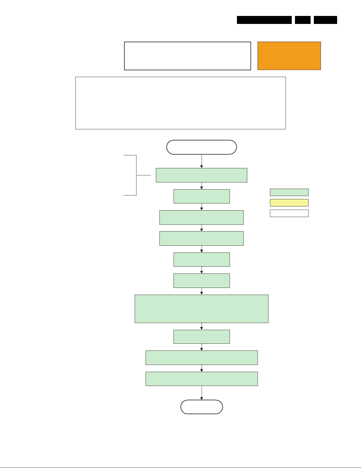
Switch on LCD lamp after valid, stable video, cor responding
to the requested output is delivered by the Viper
Active
Semi Standby
Switch off RGB blanking
Switch Audio-Reset and sound enable low and demute
(see CHS audio LdspMute interface).
Initialize audio and video processing IC's and
functions according needed use case.
Assert RGB video blanking
and audio mute
Wait until previous on-state is left more than 1
second ago. (to prevent LCD display problems)
The assumption here is that a fast toggle
(<1s) can only happen during ON->SEMI
->ON. In these states, the Viper is still
active and can provide the 1s delay. If
the transition ON->SEMI- >STBY->SEMI-
>ON can be made in less than 1s, we
have to delay the semi -> stby transition
until the requirement is met.
Constraints taken into account:
- Display may only be started when valid QVCP output clock can be delivered by the Viper.
- Between 0 and 20 ms after power is supplied, display should receive valid lvds clock.
- minimum wait time to switch on the lamp after power up is 200ms.
- RGB (on QVCP output) may be unblanked before valid output is available. Unblanking of the
picture happens with the use of the 'lamp on', not with the RGB. By doing so, black level
differencesduringstartupareavoided.
Wait until QVCP generates a valid lvds output
clock.
37" 1366*768 LCD SHARP BFI
Switch on LCD supply
(LCD-Power-on)
Start to apply valid interface signals to the module (LVDS) within a time
frame of min. 17.5ms to max. 37.5ms after supply switch on.
In implementation, use 25ms, this makes it compatible with 37HD"Sharp
(t=17.5ms is the supply switch-on delay taken into account)
NO spec yet, non BFI
version of the spec is
used
This unblank is moved forwards on demand
of SW to allow to obtain valid QVCP output
Service Modes, Error Codes, and Fault Finding
EN 29BJ3.0E LA 5.
action holder: MIPS
action holder: St-by
wait 250ms (min. = 200ms)
(lamp ready delay)
autonomous action
Figure 5-11 “Semi Stand-by” to “Active/Return” flowchart 37” 1366x768 LCD Sharp BFI display
G_15960_121.eps
100306

EN 30 BJ3.0E LA5.
action holder: St-by
32" / 42" LCD LPL scanning backlight
Switch on LCD supply
(LCD-Power-on)
Start to apply valid interface signals to the module (LVDS) within a
time frame of min. 22.5ms to max. 67.5ms after supply switch on.
In implementation, use 25ms, this makes it compatible with 32"Sharp
(t=17.5ms is the supply switch-on delay taken into account)
Active
Semi Standby
Switch off RGB blanking
Initialize audio and video processing IC's and
functions according needed use case.
Assert RGB video blanking
and audio mute
Wait until previous on-state is left more than 2
seconds ago. (to prevent LCD display problems)
The assumption he re is that a fast
toggle (<2s) can only happe n during ON-
>SEMI ->ON. In these state s, the Viper is
still active and can prov ide the 2s de lay.
If the transition ON->SEMI- >STBY->SEMI-
>ON can b e made in less than 2s, we
hav e to delay the semi -> stby transition
until the require ment is met.
Switch Audio-Reset and sound enable low and demute
(see CHS audio LdspMute interface).
Wait until QVCP generates a valid lvds output
clock.
Switch on LCD lamp after valid, stable video, corresponding
to the requested output is delivered by the Viper
Set scanning backlight to Normal scanning using the
FMS scan rate conversion interface.
This unblank is moved forwards on demand
of SW to allow to obtain valid QVCP output
To cope with the default ex-factory startup mode of
the display, the default status of the display should
be read before initializing the display. If the display
returns anything else than mode 0 (backlight off),
then mode 0 should be written in the NVM of the
display. This way of working makes sure the default
ex-factory is overwritten with the correct mode
(backlight off mode) which gives us the best startup
behaviour (dark screen) the next time the display is
started.
Display mode = 0 in
display NVM?
No
yes
Write display mode 0 to
display NVM
Service Modes, Error Codes, and Fault Finding
action holder: MIPS
autonomous action
Figure 5-12 “Semi Stand-by” to “Active” flowchart 32
” & 42” LCD LPL scanning backlight display
G_15960_122.eps
200406

Service Modes, Error Codes, and Fault Finding
action holder: St-by
Semi Standby
Active
Wait 250ms (min. = 200ms)
Switch off 12V LCD supply within a time frame of min.
0.5 ms to max. 50ms after LVDS switch off.
(Viper I/O: LCD_PWR_ON)
26" / 32" LCD LPL
Mute all sound outputs.
Mute all video outputs
switch off LCD lamp
Switch off LVDS signal
(Viper I/O: PD-LVDS)
Switch reset-audio and sound-enable
lines high
EN 31BJ3.0E LA 5.
action holder: MIPS
autonomous action
Figure 5-13 “Active” to “Semi Stand-by” flowchart 26
” & 32” LCD LPL
G_15960_126.eps
100306

EN 32 BJ3.0E LA5.
action holder: St-by
Semi Standby
Active
Wait 0ms. (No need to wait here
for the 37" Sharp panel)
Switch off 12V LCD supply within a time frame of max.
1000ms after LVDS switch off.
(Viper I/O: LCD_PWR_ON)
37" 1366*768 LCD SHARP
ASV2.3
Mute all sound outputs.
Mute all video outputs
switch off LCD lamp
Switch off LVDS signal
Switch reset-audio and sound-enable
lines high
Service Modes, Error Codes, and Fault Finding
action holder: MIPS
autonomous action
Figure 5-14 “Active” to “Semi Stand-by” flowchart 37” 1366x768 LCD Sharp ASV2.3 display
G_15960_127.eps
100306

Service Modes, Error Codes, and Fault Finding
action holder: St-by
Semi Standby
Active
Wait 0ms. (No need to wait here
for the 37" Sharp panel)
Switch off 12V LCD supply within a time frame of max.
1000ms after LVDS switch off.
(Viper I/O: LCD_PWR_ON)
37" 1366*768 LCD BFI SHARP
Mute all sound outputs.
Mute all video outputs
switch off LCD lamp
Switch off LVDS signal
Switch reset-audio and sound-enable
lines high
EN 33BJ3.0E LA 5.
action holder: MIPS
autonomous action
Figure 5-15 “Active” to “Semi Stand-by” flowchart 37
G_15960_128.eps
” 1366x768 LCD BFI Sharp display
100306

EN 34 BJ3.0E LA5.
action holder: St-by
Semi Standby
Active
Wait 250ms (min. = 200ms)
Switch off LCD supply within a time frame of min. 0.5 ms
to max. 50ms after LVDS switch off.
(Viper I/O: LCD_PWR_ON)
Mute all sound outputs.
Mute all video outputs
switch off LCD lamp
Switch off LVDS signal
(Viper I/O: PD-LVDS)
Switch reset-audio and sound-enable
lines high
32" / 42" LCD LPL scanning backlight
Service Modes, Error Codes, and Fault Finding
action holder: MIPS
autonomous action
Figure 5-16 “Active” to “Semi Stand-by” flowchart 32” & 42” LCD LPL scanning backlight display
G_15960_129.eps
100306

Service Modes, Error Codes, and Fault Finding
Images are re-transferred to DDR-RAM from
Flash RAM (verification through checksum)
Stand by
Semi Stand by
MIPS image completes the application reload,
stops DDR-RAM access, puts itself in a
sleepmode and signals the standby µP when the
standby mode can be entered.
Disable all supply related protections and switch off
the +2V5, +3V3 DC/DC converter.
DDR-RAM is put in self refresh mode and the images
are kept in the hibernating DDR-RAM.
Switch OFF all supplies by switching HIGH the POD-
MODE and the ON-MODE I/O lines.
Switch Viper in reset state
Important remark:
release reset audio and sound-
enable 10 sec after entering
standby to save power
switch off the remaining DC/DC converters
Wait 5ms
Wait 5ms
For PDP this means CPUGO
becomes low.
Wait 10ms
Switch the NVM reset line HIGH.
Delay transition until ramping down of ambient light is
finished. *)
Switch ambient light to passive mode with RGB
values on zero. *)
*) If this is not performed and the set is
switched to standby when the ramping of
the EPLD is still ongoing, the lights will
remain lit in standby.
EN 35BJ3.0E LA 5.
action holder: MIPS
transfer Wake up reasons to the
Stand by µP.
action holder: St-by
autonomous action
G_15960_133.eps
100306
Figure 5-17 “Semi Stand-by” to “Stand-by” flowchart
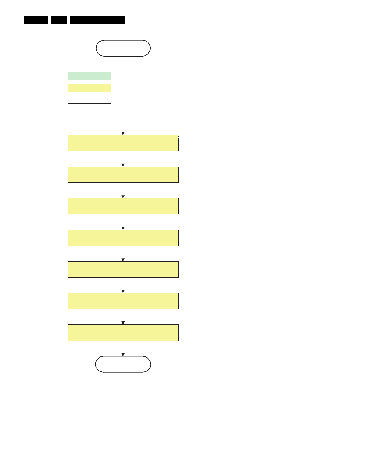
EN 36 BJ3.0E LA5.
POD standby
Semi Stand by
This state transition is entered when standby is req
uested
and an authenticated POD is present. When in semi-
standby, the CEservices will set the POD standby NVM
bit and ask infra to reboot. After the reboot, POD standby
will be entered. The Trimedia images are not started in
this case and CEsvc will ask infra to enter the Hardware
POD standby state.
Switch OFF all supplies which are not needed in POD
standby by switching HIGH the ON-MODE I/O line.
Disable +8V6 supply detection algorithm
Reboot
Power-down HDMI and 1394 hardware by keeping
POWERDOWN-1394 GPIO 0 line high.
Set Viper HW blocks (TM1, TM2, MBS, VMSP1 and
VMSP2) to powerdown mode.
Hibernate the PNX2015 memory and keep the
PNX2015 in reset state
Disable audio protection algorithm
Service Modes, Error Codes, and Fault Finding
action holder: MIPS
action holder: St-by
autonomous action
Figure 5-18 “Semi Stand-by” to “POD Stand-by” flowch
art
G_15960_134.eps
100306
Service Modes, Error Codes, and Fault Finding
POD stand by
Switch ON all supplies by switch ing LOW
the ON- MODE I/O line.
EN 37BJ3.0E LA 5.
Full SSB power and the display related supplies
Power-up HDMI and 1394 hardware by putting
Enable Viper HW blocks (TM1, TM2, MBS, VMSP1 and
(AVIP's need to be started before the MPIF's in order to have a good clock distr ibution).
AVIP default power-up mode is Standby. T he Viper instructs AVIP via I²C to enable all the
PLL's and clocks an d hence ent er to Full Powe r mode.
become available
+8V6
detected within
2000 ms after ON- MODE
toggle?
Ye s
Activate +8V6 supply
detection algorithm
Wait 2000ms to allow main supply to
deliver full power.
Enable audio protection algorithm
POWERDOWN-1394 GPIO 0 line low.
VMSP2) which we re in powerdown mode.
Release PNX2015 reset
No
+8V6 err or
SP
action holder: MIPS
action holder: St-by
autonomous action
Initialize PNX2015 HD subsystem
MPIF's should be initialized.
MPIF should d eliver 4 observers:
POR= 0 ; normal operation
MSUP = 1: Main supply is present
ASUP = 1; audio supply is present
ROK = 1; referen ce fr equency is present ( coming fro m AVIP)
All o bservers present with corr ect state? ap propriate Observer er rorNo
Ye s
Initialize tuners and Hirate
Initialize source selection
Initialize video processing IC's
- Spider
Initialize Columbus
Initialize 3D Combfilter
Initialize AutoTV
Semi-Standby
MP
G_15960_135.eps
030806
Figure 5-19 “POD Stand-by” to “Semi stand-by” flowch
art

EN 38 BJ3.0E LA5.
Service Modes, Error Codes, and Fault Finding
POD
transfer Wake up reasons to the
Stand by µP.
Images are re-transferred to DDR-RAM from
Flash RAM (verification through checksum)
MIPS image completes the application reload,
stops DDR-RAM access, puts itself in a
sleepmode and signals the standby µP when the
standby mode can be entered.
DDR-RAM is put in self refresh mode and the images
are kept in the hibernating DDR-RAM.
Wait 5ms
Switch Viper in reset state
Wait 10ms
action holder: MIPS
action holder: St-by
autonomous action
Switch the NVM reset line HIGH.
Disable all supply related protections and switch off
the +2V5, +3V3 DC/DC converter.
Wait 5ms
switch off the remaining DC/DC converters
Switch OFF all supplies by switching HIGH the POD-
MODE I/O line.
Stand by
Figure 5-20 “POD” to “Stand-by” flowchart
Important re mark:
release reset audio and sound-
enable 2 sec after entering
standby to save power
G_15960_136.eps
100306

Service Modes, Error Codes, and Fault Finding
action holder: St-by
Protection
Redefine wake up reasons for protection
state and transfer to stand-by µP.
Log the appropriate error and
set stand-by flag in NVM
MP
Ask stand-by µP to enter protection state
Flash LED in order to indicate
protection state*. (see FRS) (*): This can be the standby LED or the ON LED
depending on the availability in the set under
discussion.
SP
Switch off LCD lamp supply
Wait 250ms (min. = 200ms)
Switch off LVDS signal
Switch off 12V LCD supply within a time frame
of min. 0.5ms to max. 50ms after LVDS switch
off.
If needed to speed up this transition,
this block could be omitted. This is
depending on the outcome of the
safety investigations.
Disable all supply related protections and switch off
the +2V5, +3V3 DC/DC converter.
Switch OFF all supplies by switching HIGH the POD-
MODE and the ON-MODE I/O lines.
Switch Viper in reset state
switch off the remaining DC/DC converters
Wait 5ms
Wait 10ms
Switch the NVM reset line HIGH.
EN 39BJ3.0E LA 5.
action holder: MIPS
autonomous action
G_15960_137.eps
100306
Figure 5-21 “Protection” flowchart

EN 40 BJ3.0E LA5.
5.4 Service Tools
5.4.1 ComPair
Introduction
ComPair (Computer Aided Repair) is a service tool for Philips
Consumer Electronics products. ComPair is a further
development on the European DST (service remote control),
which allows faster and more accurate diagnostics. ComPair
has three big advantages:
1. ComPair helps you to quickly get an understanding on how
to repair the chassis in a short time by guiding you
systematically through the repair procedures.
2. ComPair allows very detailed diagnostics (on I
is therefore capable of accurately indicating problem areas.
You do not have to know anything about I2C commands
yourself because ComPair takes care of this.
3. ComPair speeds up the repair time since it can
automatically communicate with the chassis (when the
microprocessor is working) and all repair information is
directly available. When ComPair is installed together with
the Force/SearchMan electronic manual of the defective
chassis, schematics and PWBs are only a mouse click
away.
Specifications
ComPair consists of a Windows based fault finding program
and an interface box between PC and the (defective) product.
The ComPair interface box is connected to the PC via a serial
(or RS-232) cable.
For this chassis, the ComPair interface box and the TV
communicate via a bi-directional service cable via the service
connector(s).
The ComPair fault finding program is able to determine the
problem of the defective television. ComPair can gather
diagnostic information in two ways:
• Automatically (by communicating with the television):
ComPair can automatically read out the contents of the
entire error buffer. Diagnosis is done on I
ComPair can access the I2C/UART bus of the television.
ComPair can send and receive I2C/UART commands to
the microcontroller of the television. In this way, it is
possible for ComPair to communicate (read and write) to
devices on the I
• Manually (by asking questions to you): Automatic
diagnosis is only possible if the microcontroller of the
television is working correctly and only to a certain extent.
When this is not the case, ComPair will guide you through
the fault finding tree by asking you questions
screen give a picture? Click on the correct answer: YES /
NO) and showing you examples (e.g. Measure test-point I7
and click on the correct oscillogram you see on the
oscilloscope). You can answer by clicking on a link (e.g.
text or a waveform picture) that will bring you to the next
step in the fault finding process.
By a combination of automatic diagnostics and an interactive
question / answer procedure, ComPair will enable you to find
most problems in a fast and effective way.
How to Connect
This is described in the chassis fault finding database in
ComPair.
Caution: It is compulsory to connect the TV to the PC as
shown in the picture below (with the ComPair interface in
between), as the ComPair interface acts as a level shifter. If
one connects the TV directly to the PC (via UART), ICs will be
blown!
2
C/UART buses of the TV-set.
Service Modes, Error Codes, and Fault Finding
2
C level) and
Figure 5-22 ComPair interface connection
How to Order
ComPair order codes (EU/AP/LATAM):
• Starter kit ComPair32/SearchMan32 software and
ComPair interface (excl. transformer): 3122 785 90450.
• ComPair interface (excl. transformer): 4822 727 21631.
• Starter kit ComPair32 software (registration version): 3122
785 60040.
• Starter kit SearchMan32 software: 3122 785 60050.
• ComPair32 CD (update): 3122 785 60070 (year 2002),
3122 785 60110 (year 2003 onwards).
• SearchMan32 CD (update): 3122 785 60080 (year 2002),
3122 785 60120 (year 2003), 3122 785 60130 (year 2004).
• ComPair firmware upgrade IC: 3122 785 90510.
• Transformer (non-UK): 4822 727 21632.
• Transformer (UK): 4822 727 21633.
• ComPair interface cable: 3122 785 90004.
• ComPair interface extension cable: 3139 131 03791.
• ComPair UART interface cable: 3122 785 90630.
Note: If you encounter any problems, contact your local
support desk.
2
C/UART level.
(e.g. Does the
5.4.2 LVDS Tool
Introduction
This service tool (also called “ComPair Assistant 1“) may help
you to identify, in case the TV does not show any picture,
whether the Small Signal Board (SSB) or the display of a Flat
TV is defective.
Furthermore it is possible to program EPLDs with this tool (Byte
blaster). Read the user manual for an explanation of this
feature.
Since 2004, the LVDS output connectors in our Flat TV models
are standardised (with some exceptions). With the two
delivered LVDS interface cables (31p and 20p) you can cover
most chassis (in special cases, an extra cable will be offered).
When operating, the tool will show a small (scaled) picture on
a VGA monitor. Due to a limited memory capacity, it is not
possible to increase the size when processing high-resolution
LVDS signals (> 1280x960). Below this resolution, or when a
DVI monitor is used, the displayed picture will be full size.
Generally this tool is intended to determine if the SSB is
working or not. Thus to determine if LVDS, RGB, and sync
signals are okay.
How to Connect
Connections are explained in the user manual, which is packed
with the tool.
TO
UART SERVICE
CONNECTOR
PC VCR I2CPower
I2C SERVICE
CONNECTOR
9V DC
E_06532_021.eps
180804
TO

Service Modes, Error Codes, and Fault Finding
EN 41BJ3.0E LA 5.
Note: To use the LVDS tool, you must have ComPair release
2004-1 (or later) on your PC (engine version >= 2.2.05).
For every TV type number and screen size, one must choose
the proper settings via ComPair. The ComPair file will be
updated regularly with new introduced chassis information.
How to Order
• LVDS tool (incl. two LVDS cables: 31p and 20p):
3122 785 90671.
• LVDS tool Service Manual:
3122 785 00810.
• LVDS cable 31p/FI -> 31p/FI (for JL2.1 chassis):
3122 785 90861.
• LVDS cable 30p/DF -> 31p/FI (for LC4.3 chassis):
3122 785 90821.
• LVDS cable 41p/FI -> 31p/FI (dual -> single LVDS):
3122 785 90831.
• LVDS cable 20p/DF -> 20p/DF (standard with tool):
3122 785 90731.
• LVDS cable 31p/FI -> 31p/FI (standard with tool):
3122 785 90662.
• LVDS cable 20p/DF -> 20p/DF (for LC4.1 chassis):
3122 785 90851.
5.5 Error Codes
5.5.1 Introduction
The error code buffer contains all detected errors since the last
time the buffer was erased. The buffer is written from left to
right, new errors are logged at the left side, and all other errors
shift one position to the right.
When an error occurs, it is added to the list of errors, provided
the list is not full. When an error occurs and the error buffer is
full, then the new error is not added, and the error buffer stays
intact (history is maintained), except when the error is a
protection error.
To prevent that an occasional error stays in the list forever, the
error is removed from the list after more than 50 hrs. of
operation.
When multiple errors occur (errors occurred within a short time
span), there is a high probability that there is some relation
between them.
• Via the blinking LED procedure (when you have no
picture). See next paragraph.
• Via ComPair.
5.5.3 How to Clear the Error Buffer
Use one of the following methods:
• By activation of the “RESET ERROR BUFFER” command
in the SAM menu.
• With a normal RC, key in sequence “MUTE” followed by
“062599” and “OK”.
• If the content of the error buffer has not changed for 50+
hours, it resets automatically.
5.5.4 Error Buffer
In case of non-intermittent faults, clear the error buffer before
you begin the repair (before clearing the buffer, write down the
content, as this history can give you significant information).
This to ensure that old error codes are no longer present.
If possible, check the entire contents of the error buffer. In
some situations, an error code is only the result of another error
code and not the actual cause (e.g., a fault in the protection
detection circuitry can also lead to a protection).
There are several mechanisms of error detection:
• Via error bits in the status registers of ICs.
• Via polling on I/O pins going to the stand-by processor.
• Via sensing of analogue values on the stand-by processor
or the Viper.
• Via a “not acknowledge” of an I
Take notice that some errors need more than 90 seconds
before they start blinking. So in case of problems wait 2
minutes from start-up onwards, and then check if the front LED
is blinking.
2
C communication
Basically there are three kinds of errors:
• Errors detected by the Stand-by Processor. These
errors will always lead to protection and an automatic start
of the blinking LED for the concerned error (see paragraph
“The Blinking LED Procedure”). In these cases SDM can
be used to start up (see chapter “Stepwise Start-up”). Note
that it can take up to 90 seconds before the TV goes to
protection and starts blinking the error (e.g. error 53)
• Errors detected by VIPER that lead to protection. In this
case the TV will go to protection and the front LED should
also blink the concerned error. Depending on the software
version it is possible that this mechanism does not work.
See also paragraph “Error Codes” -> “Error Buffer” ->
“Extra Info”.
• Errors detected by VIPER that do not lead to
protection. In this case the error will be logged into the
error buffer and can be read out via ComPair, via blinking
LED method, or in case you have picture, via SAM.
5.5.2 How to Read the Error Buffer
Use one of the following methods:
• On screen via the SAM (only if you have a picture). E.g.:
– 00 00 00 00 00: No errors detected
– 06 00 00 00 00: Error code 6 is the last and only
detected error
– 09 06 00 00 00: Error code 6 was first detected and
error code 9 is the last detected error

EN 42 BJ3.0E LA5.
Service Modes, Error Codes, and Fault Finding
Table 5-2 Error code overview
Error Description Error/Prot Detected by Device Defective module Result
1
I2C1
2
I2C2
3
I2C3
4
I2C4
5 VIPER does not boot P Stby µP PNX8550 / Protection + Error blinking
6 5V supply P Stby µP / / Protection + Error blinking
7 8V6 supply P Stby µP / / Protection + Error blinking
8 1.2V DC/DC P Stby µP / / Protection + Error blinking
11 3.3V DC/DC P Stby µP / / Protection + Error blinking
12 12V supply P Stby µP / / Protection + Error blinking
14 Audio P Stby µP / / Protection + Error blinking
18 MPIF1 ref. freq. E VIPER PNX3000 IF I/O Error logged
25 Supply fault P Stby µP n.a. / Protection + Error blinking
27 PNX2015 HD subsystem part E VIPER / / see extra info
29 AVIP 1 E VIPER / / see extra info
31 AVIP 2 E VIPER / / see extra info
32 MPIF1 E VIPER PNX3000 analogue 1 front end 1 Error logged
34 Tuner1 E VIPER / Tuner 1 Error logged
36 OFDM (channel decoder) E VIPER TDA10046 / Error logged
39 POD/Common Interface E V IPER STV0701 / Error logged
43 Hi Rate Front End E VIPER TDA9975 HDMI Error logged
44 NVM P Stby µP / / see extra info
45 Columbus 1 E VIPER PNX2015 Comb filter Error logged
46 Pacific 3 E VIPER / / TV to standby + Error logged
53 VIPER P Stby µP PNX8550 / Protection + Error blinking
55 Spider E VIPER / / see extra info
63 Power OK P VIPER / / Protection + Error blinking (see extra info)
64 Display E VIPER / / Error logged
P VIPER /
E VIPER /
P Stby µP / / Protection + Error blinking
P VIPER /
I2C1_blocked
I2C2_blocked
I2C4_blocked
Protection + Error blinking
Error logged
Protection + Error blinking
Extra Info
• Rebooting. When a TV is constantly rebooting due to
internal problems, most of the time no errors will be logged
or blinked. This rebooting can be recognised via a ComPair
interface and Hyperterminal (for Hyperterminal settings,
see paragraph “Stand-by software upgrade). You will see
that the loggings which are generated by the main software
keep continuing. In this case (rebooting) diagnose has to
be done via ComPair.
• Error 1 (I
2
C bus 1 blocked). When this error occurs, the
TV will go to protection and the front LED will blink error 1.
Now you can start up the TV via the SDM short-cut pins on
the SSB. The TV will start up and ignore the error.
Depending on the problem it is even possible that you have
picture.
• Error 2 (I
2
C bus 2 blocked). Due to hardware restriction
(I2C bus 2 is the fast I2C bus) it will be impossible to start
up the VIPER when I2C bus 2 is blocked. When this error
occurs, the TV will not start up (but probably you will see
the green LED). Starting up the TV via the SDM short-cut
pins will not work. So it will not be possible to read out error
2 via internal software (allthough it will be logged). Use
ComPair for further diagnose (e.g. read out the NVM
content).
• Error 3 (I
2
C bus 3 blocked). There are only three devices
on I2C bus 3: VIPER, Stand-by Processor, and NVM. The
Stand-by Processor is the detection device of this error, so
this error will only occur if the VIPER or the NVM is blocking
the bus. This error will also blink when the NVM gives no
acknowledge on the I
2
C bus. Note that if the 12 V supply is
missing, the DC/DC supply on the SSB will not work.
Therefore the VIPER will not get supplies and could block
2
I
C bus 3. So, a missing 12 V can also lead to an error 3.
• Error 4 (I2C bus 4 blocked). When this error occurs, the
TV will go to protection and the front LED will blink error 4.
Now you can start up the TV via the SDM short-cut pins on
the SSB. The TV will start up and ignore the error.
Depending on the problem it is even possible that you have
picture.
• Error 5 (VIPER does not boot). This error will point to a
severe hardware problem around the VIPER (supplies not
OK, VIPER completely dead, I
2
C link between VIPER and
Stand-by Processor broken, etc...).
• Error 7 (8V6 error). In case of a TV with SDI display you
will see error 7 blink in case of an audio protection. So
except a problem with the 8V6 itself it is also possible that
there is something wrong with the audio part. See also
paragraph "Hardware Protections" for this.
• Error 14 (Audio protection). The detection is done on the
audio board itself. Several items are monitored:
overvoltage, overcurrent, DC level on the speakers and the
audio supply voltages. If one of these items fails, the
audioprotection will switch off the main supply. All supplies
will drop, the standby processor “thinks” there is a mains
dip, and will reboot. At the beginning of the boot process,
the audio-protection line is monitored: if this line is “active”,
the set will go to protection and will blink error 14.
• Error 27 (PNX2015 HD subsystem part). Diagnosing this
error will not be possibly via the normal errorcodes. In case
this device can not communicate with the Viper via I²C, it
will not be possible to initialise the tunnelbus. Hence the
software will not be able to start up, and will re-boot
constantly. Diagnosing these problems will only be
possible via ComPair. In theory it is possible that the error
is logged in the NVM (that’s why this error is still mentioned
here).
• Error 29 (AVIP 1). Same remark as for error 27.
• Error 31 (AVIP 2). Same remark as for error 27.
• Error 44 (NVM). This error will probably never occur
because it is masked by error 3 (I
2
C bus 3). The detection
mechanism for error 3 checks on an I2C acknowledge of
the NVM. If NVM gives no acknowledge, the stand-by
software assumes that the bus is blocked, the TV goes to
protection and error 3 will be blinking..
• Error 46 (Pacific 3). When this errors occurs the TV will go
to stand-by. The reason for this is, when there is an
occasional boot problem of the Pacific, it will look like the
TV has started up in stand-by mode, and the customer can
switch it on again. When there is an actual problem with or
around the Pacific the TV will go to stand-by every time you
try to start up. So this behaviour is an indication of a Pacific
problem.

Service Modes, Error Codes, and Fault Finding
EN 43BJ3.0E LA 5.
• Error 53. This error will indicate that the VIPER has started
to function (by reading his boot script, if this would have
failed, error 5 would blink) but initialization was never
completed because of hardware peripheral problems
(NAND flash, ...) or software initialization problems.
Possible cause could be that there is no valid software
loaded (try to upgrade to the latest main software version).
Note that it takes 90 seconds before the TV goes to
protection in this case.
• Error 55 (SPIDER error). Same remark as for error 27.
• Error 63 (POWER OK). When this error occurs, it means
that the POWER-OK line did not became “high”. This error
is only applicable for TV’s with a SDI display, a FHP display
or a Sharp full HD display. Depending on the software
version it is possible that the detection mechanism of this
error does not function and that the TV keeps rebooting.
• Error 64 (Display error). When this error occurs it means
that there is a problem with the I
the display. Allthough several display types communicate
2
via I
C, this error will only work for TV’s with a FHP display.
2
C communication towards
5.6 The Blinking LED Procedure
5.6.1 Introduction
The blinking LED procedure can be split up into two situations:
• Blinking LED procedure in case of a protection detected by
the stand-by processor. In this case the error is
automatically blinked. This will be only one error, namely
the one that is causing the protection. Therefore, you do
not have to do anything special, just read out the blinks. A
long blink indicates the decimal digit, a short blink indicates
the units.
• Blinking LED procedure in the “on” state. Via this
procedure, you can make the contents of the error buffer
visible via the front LED. This is especially useful for fault
finding, when there is no picture.
When the blinking LED procedure is activated in the “on” state,
the front LED will show (blink) the contents of the error-buffer.
Error-codes > 10 are shown as follows:
1. “n” long blinks (where “n” = 1 - 9) indicating decimal digit,
2. A pause of 1.5 s,
3. “n” short blinks (where “n”= 1 - 9),
4. A pause of approx. 3 s.
5. When all the error-codes are displayed, the sequence
finishes with a LED blink of 3 s,
6. The sequence starts again.
Example: Error 12 8 6 0 0.
After activation of the SDM, the front LED will show:
1. 1 long blink of 750 ms (which is an indication of the decimal
digit) followed by a pause of 1.5 s,
2. 2 short blinks of 250 ms followed by a pause of 3 s,
3. 8 short blinks followed by a pause of 3 s,
4. 6 short blinks followed by a pause of 3 s,
5. 1 long blink of 3 s to finish the sequence,
6. The sequence starts again.
second last error, etc.... Take notice that it takes some
seconds before the blinking LED starts.
5.7 Protections
5.7.1 Software Protections
Most of the protections and errors use either the stand-by
microprocessor or the VIPER controller as detection device.
Since in these cases, checking of observers, polling of ADCs,
filtering of input values are all heavily software based, these
protections are referred to as software protections.
There are several types of software related protections, solving
a variety of fault conditions:
• Protections related to supplies: check of the 12V, +5V,
+8V6, +1.2V and +3.3V.
• Protections related to breakdown of the safety check
mechanism. E.g. since a lot of protection detections are
done by means of the VIPER, failing of the VIPER
communication will have to initiate a protection mode since
safety cannot be guaranteed any more.
Remark on the Supply Errors
The detection of a supply dip or supply loss during the normal
playing of the set does not lead to a protection, but to a cold
reboot of the set. If the supply is still missing after the reboot,
the TV will go to protection.
Protections during Start-up
During TV start-up, some voltages and IC observers are
actively monitored to be able to optimise the start-up speed,
and to assure good operation of all components. If these
monitors do not respond in a defined way, this indicates a
malfunction of the system and leads to a protection. As the
observers are only used during start-up, they are described in
the start-up flow in detail (see paragraph “Stepwise Start-up").
5.7.2 Hardware Protections
There are no real hardware protections in this chassis..
Allthough, in case of an audio problem, the audio protection
circuit will switch off the main supply. The stand-by
microprocessor will interpret this as a mains dip and will try to
start up again.
In case of a TV with SDI display this will probably lead to
protection error 7 (8V6 error) and an internal error 11 (so it
looks like an overvoltage protection of the SDI supply itself).
In other cases it will lead to error 14 (audio protection).
Repair Tips
• It is also possible that you have an audio DC protection
because of an interruption in one or both speakers (the DC
voltage that is still on the circuit cannot disappear through
the speakers).
5.6.2 How to Activate
Use one of the following methods:
• Activate the SDM. The blinking front LED will show the
entire contents of the error buffer (this works in “normal
operation” mode).
• Transmit the commands “MUTE” - “062500” - “OK”
with a normal RC. The complete error buffer is shown.
Take notice that it takes some seconds before the blinking
LED starts.
• Transmit the commands “MUTE” - “06250x” - “OK”
with a normal RC (where “x” is a number between 1 and
5). When x= 1 the last detected error is shown, x= 2 the

EN 44 BJ3.0E LA5.
5.8 Fault Finding and Repair Tips
Read also paragraph "Error Codes" - "Extra Info".
32" LCD
Power supply start-up behaviour
Service Modes, Error Codes, and Fault Finding
Power Supply Check
Mains cord is connected
N
SSB Board defective
Standby command linefrom PNX
BLR Procedure
SSB Start-up process
12V and 5V switched to DC/DC
converters on SSB start up via
Standby processor (PNX)
LED is on?
Y
Red LED is on +5V2 is ok.
Standby supply is working
Switch set on via Local keyboard or RC
Standby line goes
low pin 7 1M03
Relay on Display supply is closed
LLC supply starts
+12V, & +8V6 becomes available connector 1M46
+24V (or 295V) for Backlights connector 1319
OK
Voltages on
1M46?
No
Check if vacation switch is closed
+5V2 is OK?
Pin 7 1M46
Y
Check Fuse 1400 & 1401 , on Mains filter supply
Drive circuit 7100 & T 7102
and components in standby supply
Not OK
No start-up of Display supply check
No
Check Standby supply
Check 25V Hot, 400V Hot
Protection?
Blinking LED?
Y
If protection blinking LED.
Check if error code is related to
DC/DC converter on SSB
Error code is
from DC/DC ?
Y
Change SSB
BLR procedure
No
No
SSB Start-up process Continue
Viper & I2C commands
switching VDisplay voltage to LVDS
connector
In case of short circuit on VDisplay
PS, disconnect LVDS cable
Figure 5-23 First line fault find tree 32” LCD
LLC supply
is working?
Y
Check output voltage.
LCD Inverter start up process
from SSB.........
Check LLC Display supply
Drive 7001, Mosfet 7005, 7006
OVP Latch
If protection blinking LED
Check protection error code = xx xx xx
is 12V or DC protection(Audio)?
Disconnect PS connector to Audio part &
backlight inverters. Try again
N
Check OVP Latch
LLC supply components, control
Check PS in standalone mode
circuit....
(disconnect display supply
connectors)
G_15970_032.eps
120506
Service Modes, Error Codes, and Fault Finding
EN 45BJ3.0E LA 5.
37" LCD
Power supply start-up behaviour
Switch set on via Local keyboard or RC
N
SSB Board defective
Standby command linefrom PNX
BLR Procedure
+5V-SW, +12V, & +8V6 becomes available
Power Supply Check
Mains cord is connected
LED is on?
Y
Red LED is on +5V2 is ok.
Standby supply is working
Standby line goes
low pin 7 1M03
Y
from platform supply
Check on connector 1M46
No
Check if vacation switch is closed
+5V2 is OK?
Pin 7 1M46
Y
Check Standby supply on platform
Check Fuse 1400, on Diplay supply
and components in standby supply
No
400VF = 295V on fuse 1P03
Drive circuit, T 7S02
SSB Start-up process
DC/DC converters start up via
Standby processor
Protection?
Blinking LED?
Y
Check if error code is related to
DC/DC converter on SSB
Error code is
from DC/DC ?
Y
Change SSB
BLR procedure
Y
No
SSB Start-up process Continue
Viper & I2C commands
switching VDisplay voltage to LVDS
connector
In case of short circuit on VDisplay
PS, disconnect LVDS cable
Power OK platform
pin 2 1M03 is OK?
Display supply starts-up
Relay on Display supply is closed
LLC supply starts
No
LLC supply
is working?
No
Y
Y
Check output voltage.
LCD Inverter start up process
from SSB.........
No start-up of platform supply check
+Vaux from standby supply
Check platform supply
Drive 7P27, Vcc = 15V
Switch on control part 7P12 & 7P26
If protection blinking LED
Check protection error code = xx xx xx
is related to platform supply
Disconnect PS connector To Audio if error code is
Disonnect PS to Ambilight 1M10 & 1M18.
N
Audio protection.
Try again
Check OVP Latch
+25V Hot and 400V Hot
LLC supply components, control
circuit....
Check PS in standalone mode
(disconnect display supply
connectors)
G_15970_033.eps
120506
Figure 5-24 First line fault find tree 37” LCD

EN 46 BJ3.0E LA5.
Service Modes, Error Codes, and Fault Finding
5.8.1 Exit “Factory Mode”
When an "F" is displayed in the screen's right corner, this
means that the set is in "Factory" mode, and it normally
happens after a new SSB has been mounted.
To exit this mode, push the "VOLUME minus" button on the
TV's keyboard control for 5 seconds and restart the set.
When a DVBT TV starts up in factory mode, the TV will tune to
preset 0. When there is no channel installed on preset 0, there
will be no picture and it will look like the set is in standby mode.
De-activating factory mode can also be done via the above
method.
5.8.2 MPIF
Important things to make the MPIF work:
• Supply.
• Clock signal from the AVIP.
2
• I
C from the VIPER.
When there is no sound an external sources, check the audio
supply of the MPIF.
5.8.3 AVIP
Important things to make the AVIP work:
• Supplies.
• Clock signal from the VIPER.
2
• I
C from the VIPER (error 29 and 31).
5.8.4 PACIFIC 3
In case the Pacific fails, the TV will go to stand-by. The reason
for this is, when there is an occasional boot problem of the
Pacific, it will look like the TV has started up in stand-by mode,
and the customer can switch it on again. When there is an
actual problem with or around the Pacific the TV will go to
stand-by every time you try to start up. So this behaviour is an
indication of a Pacific problem.
5.8.5 Ambilight
Note: in case of Ambilight protection, the TV itself will not go to
protection, only the Ambilight board. When you disconnect the
TV from the mains and reconnect again, the Ambilights will
work again.
In case of multiple protections, check and replace the invertor
transformers and/or the lamp unit(s).
Protections on the ambilight boards:
Parallel arcing protection.In normal operation the inverter
frequency is ±63 kHz. In case of short circuit of the transformer
output the frequency is >100 kHz. Protection is done via
sensing the switching frequency.
Serial arcing protection. The detection of the arcing is done
in the ground wire of lamp units. The µProcessor is counting the
protection pulses. When 50 pulses are counted within 2
seconds protection will be triggered.
5.8.6 Sanken display supply.
All 42” LCD sets for this chassis have a Sanken display supply.
If this supply fails there will be no error or protection because
there is no feedback foreseen from the supply towards the
SSB. The result of a failing Sanken display supply could be that
there is no picture, but that you will probably have sound and 1
out of 3 ambilights will still work (in case ambilight is switched
on).
5. Check the over-current detection circuit (2U18 or 3U83 interrupted).
Another result of a failing Sanken display is of course that the
set is completely dead.
When the primary circuit of the platform supply fails, there is a
high possibility that the main fuse of the Sanken display supply
will break. In this case the Sanken supply must not be replaced
completely. That fuse can be ordered separately (order code
2422 086 00689, Bel Fuse 5x20 HT 6A3 250 V). For safety
reasons, make sure to use the correct fuse type.
5.8.7 DC/DC Converter
Introduction
• The best way to find a failure in the DC-DC converters is to
check their starting-up sequence at power-on via the mains
cord, presuming that the standby PP is operational.
• If the input voltage of DC-DC converters is around 12V
(measured on decoupling capacitors 2U17/2U25/2U45)
and the enable signals are low (active) then the output
voltages should have their normal values. First, the
standby PP activates the +1V2 supply (via ENABLE-1V2)
then, after this voltage becomes present and is detected
OK (about 100ms), the other two voltages (+2V5 and
+3V3) will be activated (via ENABLE-3V3). The Vtun
generator (present only for the analogue version of Jaguar
Baby) will generate +33V for the analogue tuner as soon as
the 12V/3.3V DC-DC converter will start operating.
• The consumption of controller IC 7U00 is around 30mA
(that means around 300mV drop voltage across resistor
3U22).
• The current capability of DC-DC converters is quite high
(short-circuit current is 7 to 10A), therefore if there is a
linear integrated stabilizer that, for example delivers 1.8V
from +3V3 with its output overloaded, the +3V3 stays
usually at its normal value even though the consumption
from +3V3 increases significantly.
• The +2V5 supply voltage is obtained via a linear stabilizer
made with discrete components that can deliver a lot of
current, therefore in case +2V5 (or +2V5D) is shortcircuited to GND then +3V3 will not have the normal value
but much less. There is a +2V5D low power linear stabilizer
(to supply the DDR memories in standby mode) that is not
used. In normal operation mode the value of this supply
voltage will be close to +2V5 (20..30 mV difference).
• The supply voltages +5V and +8V6 are available from
connector 1M46; they are not protected by fuses. +12VSW
is protected for over-currents by the fuse 1U04 while 1U01
is protecting in case of defects in DC-DC converters. There
are on-board switches for +8V6-SW (see "DC-DC
CONNECTIONS" schematic) and +12VSW but they are
not used (by-passed).
Fault Finding
• Symptom: +1V2, +2V5 and +3V3 not present (even for a
short while ~10ms)
1. Check 12V availability (fuse 1U01, resistor 3U22,
power MOS-FETs) and enable signal ENABLE-1V2
(active low),
2. Check the voltage on pin 9 (1.5V),
3. Check for +1V2 output voltage short-circuit to GND that
can generate pulsed over-currents 7...10A through coil
5U03,
4. Check the over-current detection circuit (2U12 or 3U97
interrupted).
• Symptom: +1V2 present for about 100ms, +2V5 and +3V3
not rising
1. Check the ENABLE-3V3 signal (active LOW),
2. Check the voltage on pin 8 (1.5V),
3. Check the under-voltage detection circuit (the voltage
on collector of transistor 7U10-1 should be less than
0.8V),
4. Check for output voltages short-circuits to GND (+3V3,
+2V5 and +2V5D) that can generate pulsed overcurrents 7...10A through coil 5U00,

Service Modes, Error Codes, and Fault Finding
E_14700_082.eps
120505
Partition 1
Trimedia2 image
Trimedia1 image
MIPS image
Partition 0
USB Download Application
uBTM (boot block)
USB CUSTOMER
USB SERVICE
EJTAG
EN 47BJ3.0E LA 5.
• Symptom: +1V2 OK, +2V5 and +3V3 present for about
100ms. Cause: SUPPLY-FAULT line stays low even
though the +3V3 and +1V2 is available - the standby PP is
detecting that and switching off all supply voltages.
1. Check the value of +2V5 and the drop voltage across
resistor 3U22 (they could be too high),
2. Check if +1V2 or +3V3 are higher than their normal
values - that can be due to defective DC feedback of
the respective dc-dc converter (ex. 3U18 or 3UA7).
• Symptom: +1V2, +2V5 and +3V3 look ok, except the
ripple voltage that is increased (audible noise can come
from the filtering coils 5U00 or 5U03).
Cause: instability of the frequency and/or duty cycle of one
or both dc-dc converters.
1. Check the resistor 3U06, decoupling capacitors, AC
feedback circuits (2U20 + 2U21 + 3U14 + 3U15 for
+1V2 or 2U19 + 2U85 + 3U12 + 3U13 for +3V3),
compensation capacitors 2U09, 2U10, 2U23 and
2U73, IC 7U00.
• Symptom: +1V2, +2V5 and +3V3 ok, no +Vtun (analogue
sets only). Cause: the “VTUN GENERATOR” circuit
(second schematic) is defective.
1. Check transistor 7U24 (has to have gate pulses of
about 10V amplitude and drain pulses of about 35V
amplitude) and surrounding components.
Note: fuse 1U01 broken means usually a pair of power MOSFETs (7U01 or 7U03) defective. The IC 7U00 should be
replaced as well in this case
5.9 Software Upgrading
5.9.1 Introduction
5.9.2 Main Software Upgrade
The software image resides in the NAND-Flash, and is
formatted in the following way:
Figure 5-25 NAND-Flash format
Executables are stored as files in a file system. The boot loader
(uBTM) will load the USB Download Application in partition 0
(USB drivers, boot script, etc.). This application makes it then
possible to upgrade the main software via USB.
Installing "Partition 0" software is possible via an external
EJTAG tool, but also in a special way with the USB stick (see
description in paragraph “Partition 0“).
Partition 1 (Customer)
To do a main software upgrade (partition 1) via USB, the set
must be operational, and the "Partition 0" files for the VIPER
must be installed in the NAND-Flash!
The set software and security keys are stored in a NANDFlash, which is connected to the VIPER via the PCI bus.
It is possible for the user to upgrade the main software via the
USB port. This allows replacement of a software image in a
stand alone set, without the need of an E-JTAG debugger. A
description on how to upgrade the main software can be found
in chapter 3 "Directions For Use".
Important: When the NAND-Flash must be replaced, a new
SSB must be ordered, due to the presence of the security
keys!!! (copy protection keys, MAC address, for US the POD
keys, ...). See table “SSB service kits” for the order codes.
Perform the following actions after SSB replacement:
1. Set the correct option codes (see sticker inside the TV).
2. Update the TV software (see chapter 3 for instructions).
3. Perform the alignments as described in chapter 8.
4. Check in CSM if the HDMI keys are valid.
Table 5-3 SSB service kits
Model Number
26PF9531/10 3104 328 49621 3104 328 47161
26PF9631D/10
32PF9541/10
32PF9631D/79
32PF9641D/10
32PF9968/10
37PF9631D/10
37PF9631D/79
42PF7621D/10
42PF9641D/79
SSB factory assy code
3104 328 49691 3104 328 47172
3104 328 49721 3104 328 49551
3104 328 44001 3104 328 47153
3104 328 49731 3104 328 49561
3104 328 49631 3104 328 47171
3104 328 49591
3104 328 44001 3104 328 47153
3104 328 49701 3104 328 48261
3104 328 44001 3104 328 47153
1).
New SSB order code
3104 328 47151
1). Information in column “SSB factory assy code” is only for
reference purposes. Do not use this code when ordering a new
SSB.
The new software can be uploaded to the TV by using a
portable memory device or USB storage compliant devices
(e.g. USB memory stick). You can download the new software
from the Philips website to your PC.
Partition 0 (Service)
If the "Partition 0" software is corrupted, the software needs to
be re-installed.
To upgrade this “USB download application” (partition 0 except
the boot block), insert an USB stick with the correct software,
and press the “red” button on the remote control (in ”TV” mode)
when it is asked via the on screen text.
Caution:
• The USB download application will now erase both
partitions (except the boot block), so you need to reload the
main SW after upgrading the USB download application.
As long as this is not done, the USB download application
will start when the set is switched “on”.
• When something goes wrong during the progress of this
method (e.g. voltage dip or corrupted software file), the set
will not start up, and can only be recovered via the EJTAG
tool!
5.9.3 Manual Start of the Software Upgrade Application
Normally, the software upgrading procedure will start
automatically, when a memory device with the correct software
is inserted, but in case this does not work, it is possible to force
the TV into the software upgrade application. To do so:
• Disconnect the TV from the Mains/AC Power.
• Press the “OK” button on a Philips DVD RC-6 remote
control (it is also possible to use the TV remote in "DVD"
mode).
• Keep the “OK” button pressed while connecting the TV to
the Mains/AC Power.
• The software upgrade application will start.
• When a memory device with upgrade software is
connected, the upgrade process will start.

EN 48 BJ3.0E LA5.
5.9.4 Stand-by Software Upgrade
There are two methods now to upgrade stand-by software:
Upgrade via USB
In this chassis it is possible to upgrade stand-by software via a
USB stick. The method is similar to upgrading main software
via USB.
Use the following steps:
1. Create a directory “upgrades” on your USB stick.
2. Copy the stand-by software (delivered via the Service
organisation) into this directory.
3. Insert the USB stick into the TV.
4. Start the download application manually (see paragraph
“Manual start of the Software Upgrade Application”).
5. Select the appropriate file and press the red button to
upgrade:
Upgrade via PC and ComPair interface
It will be possible to upgrade the Stand-by software via a PC
and the ComPair interface. Check paragraph "ComPair" on
how to connect the interface. To upgrade the Stand-by
software, use the following steps:
1. Disconnect the TV from the Mains/AC Power.
2. Short circuit the SPI pins [2] on the SSB. They are located
outside the shielding (see figure “Service mode pads”).
3. Keep the SPI pins shorted while connecting the TV to the
Mains/AC Power.
4. Release the short circuit after approx. two seconds.
5. Start up HyperTerminal (can be found in every Windows
application via Programs -> Accessories ->
Communications -> HyperTerminal). Use the following
settings:
– COM1
– Bits per second = 38400 (9600)*
– Data bits = 8
– Parity = none
– Stop bits = 1
– Flow control = None
6. Press “Shift U” on your PC keyboard. You should now see
the following info:
– PNX2015 Loader V1.0
– 19-09-2003
– DEVID=0x05
– Erasing
– MCSUM=0x0000
– =
7. If you do not see the above info, restart the above
procedure, and check your HyperTerminal settings and the
connections between PC and TV.
8. Via “Transfer” -> “Send text file ...”, you can send the
proper upgrade file to the TV (e.g. *.hex). This file will be
distributed via the Service Organization.
9. After successful programming, you must see the following
info (this can take several minutes!):
– DCSUM=0xECB3
– :Ok
– MCSUM=0xECB3
– Programming
– PCSUM=0xECB3
– Finished
10. If you do not see this info, restart the complete procedure.
11. Close HyperTerminal.
12. Disconnect and connect Mains/AC Power again.
Service Modes, Error Codes, and Fault Finding
(*) When having problems with upgrading, use the values
between brackets.

Block Diagrams, Test Point Overviews, and Waveforms
49BJ3.0E LA 6.
6. Block Diagrams, Test Point Overviews, and Waveform
s
Wiring Diagram 26” ME5P
1M03
10P
1M46
11P
1M03
10P
1M46
11P
1M52
9P
1M52
9P
1M36
11P
CONTROL BOARD
E
SMALL SIGNAL BO
ARD
B
1736
3P
1735
3P
SPEAKER RIGHT SPEAKER LEFT
LCD SUPPLY / STANDBY / AUDIO
AC
1304
11P
1684
3P
1M013P1M21
6P
1870
6P
1319
14P
1316
12P
1319
14P
1316
12P
G_15950_034.eps
010906
IR/LED
J
REAR FACING SA
V
D
LVDS
31P
1G50
31P
1H01
4P
USB
WIRING 26” (STYLING ME5P)
1308
2P3
INLET
1E40
40P
1E40
40P
1E62
20P
1E62
20P
8101
8736
8735
8152
8150
8201
8136
8240
8262
8316
8146
8103
8319
8121
8408
4P
USB
50BJ3.0E LA 6.
Block Diagrams, Test Point Overviews, and Waveforms
Wiring Diagram 32” Soft Wrap 2k5
G_15950_035.eps
010906
LS
RIGHT
LS
LEFT
L
S
RIGHT
LS
0345
6P
CONTROL BOARD
E
LED PANEL
J
1M37
11P
1H01
(USB)
4P
SIDE I/O
D
ST
ANDBY / AUDIO
SA
MAIN SUPPLY
A
0345
6P
1H01
4P
USB
1G50
31P
SMALL SIGNAL BOARD
B
EXTERNALS
BE
1M20
12P
1M36
11P
1M52
9P
1E40
40P
1E62
20P
1E62
20P
8262
1E40
40P
1M46
11P
1M03
10P
1M59
5P
1M63
3P
1319
14P
1M64
9P
1306
2P3
1M03
10P
1305
3P
1M02
7P
1305
3P
1308
2P
1M46
11P
1M64
9P
1306
2P3
1735
2P3
1736
2P3
1M02
7P
1M52
9P
1M10
6P
DISPLAY
14P
LVDS
31P
AC INLET
8191
8192(UK)
8736
8120
8735
8345
8136
8201
8306
8305
8364
8319
8302
8146
8103
8152
8250
8408
8240
1M64
4P
1N62
4P
8264
WIRING 32” (STYLING SOFT WRAP 2K5)
1M20
12P
INVERTER
Block Diagrams, Test Point Overviews, and Waveforms
S
RIGHT
LS
SIDE I/O
D
0345
6P
CONTROL BOARD
E
LED PANEL
J
1M37
11P
1H01
(USB)
4P
STANDBY / AUDIO
SA
MAIN SUPPLY
A
0345
6P
1H01
4P
USB
1G50
31P
SMALL SIGNAL BOARD
B
EXTERNALS
BE
1M20
12P
1M36
11P
1M52
9P
1E40
40P
1E62
20P
1E62
20P
8262
1E40
40P
1M46
11P
1M03
10P
1M59
4P5
1M63
3P
1319
14P
1M64
9P
1306
2P3
1M03
10P
1305
3P
1M02
7P
1305
3P
1308
2P
1M46
11P
1M64
9P
1306
2P3
1735
2P3
1736
2P3
1M02
7P
1M52
9P
DISPLAY
14P
LVDS
30P
AC INLET
8191
8192(UK)
8736
8120
8735
8345
8136
8201
8306
8305
8364
8319
8302
8146
8103
8152
8250
8408
8240
1M64
4P
1N62
4P
8264
WIRING 32” (STYLING STEP 2K4)
1M20
12P
INVERTER
AMBIL LIGHT RIGHT
AMBIL LIGHT LEFT
AMBI
LIGHT
AL
1M11
11P
1M12
3P
1M49
4P
1M104P1M08
4P
1004
5P
1M48
3P
AMBI
LIGHT
AL
1M11
11P
1M12
3P
1M49
4P
1M10
4P
1M08
4P
1004
5P
1M48
3P
INVERTER
DISPLAY
12P
1M08
4P6
1317
12P
8608
8548
8508
8559
Wiring Diagram 32” Step 2k4
51BJ3.0E LA 6.
RIGHT
LS
L
LS
LEFT
G_15951_012.eps
010906
Block Diagrams, Test Point Overviews, and Waveforms
Wiring Diagram 32” Step 2k6
WIRING 32” (STYLING STEP 2K6)
52BJ3.0E LA 6.
AL
AMBI LIGHT
3P
1M16
11P
1M11
3P
1M15
11P
1M13
AMBILIGHT UNIT RIGHT
CONTROL BOARD
E
1M01
3P
8101
J
LED PANEL
1M39
1M59
1M49
1M10
1M09
1M08
1M21
8508
3P
5P
4P
6P
4P
6P
14P
1319
8121
6P
6P
1M10
8510
9P
1M52
7P
1M02
8559
11P
1M46
B
SMALL SIGNAL BOARD
8735
SA
ST
ANDBY / AUDIO
1735
2P3
10P
1M03
8103
1M63
1736
2P3
8146
5P
3P
1M59
8736
USB
1H01
8549
8152
31P
4P
1G50
4P
1M64
8264
4P
1N62
1E62
8302
2P
1306
3P
1305
9P
1M64
10P
11P
1M03
1M46
9P
1M52
1E40
40P
8240
20P
8262
8150
BE
8319
8306
8364
LVDS
31P
11P
1M36
40P
1E40
EXTERNALS
20P
1E62
7P
1M02
14P
1319
A
MAIN SUPPLY
8305
9P
1M64
AL
AMBI LIGHT
6P
1M08
4P
1M09
6P
1M10
4P
1M49
4P5
1M59
3P
1M39
1M13
1M15
1M11
1M16
11P
3P
11P
3P
AMBILIGHT UNIT LEFT
3P
1M216P1M01
2P
1306
3P
1305
D
SIDE I/O
1H01
(USB)
2P
1308
8408
8201
8136
AC INLET
8191
8192(UK)
8194(AUS/NZ)
4P
11P
1M37
SPEAKER RIGHT SPEAKER LEFT
G_15970_024.eps
010906
Block Diagrams, Test Point Overviews, and Waveforms
Wiring Diagram 37” 2k6
WIRING 37” (STYLING STEP 2K6)
53BJ3.0E LA 6.
8320
8549
8508
AL
AMBI
LIGHT
1M39
3P
1M16
1M59
1M49
11P
1M11
1M10
3P
1M15
1M09
1M08
11P
1M13
AMBILIGHT UNIT RIGHT
CONTROL BOARD
E
1M01
3P
8101
8510
7P
3P
5P
4P
C
8302
Shielding
8735
AUDIO
1736
9P
1735
1M52
1M02
7P
11P
10P
1M46
1M03
B
SMALL SIGNAL BO
LVDS
2P
2P
8150
8103
8146
8152
1H01
8201
9P
1E62
1M52
1E40
40P
8240
20P
31P
4P
1G50
USB
4P
1M64
1M63
8559
4P5
3P
1M59
ARD
31P
8121
6P
3P
11P
1M21
1M01
1M36
40P
1E40
BE
1N62
8264
4P
8262
EXTERNALS
20P
1E62
6P
14P
1320
4P
6P
1M02
6P
1M10
4P
1M18
A
10P
1M03
11P
14P
1M46
3P
1M63
DISPLAY SUPPLY
PLATFORM SUPPLY
14P
1320
8319
1319
AL
AMBI
LIGHT
6P
1M08
11P
1M13
4P
1M09
1M10
1M49
1M59
1M39
1M15
1M11
1M16
3P
11P
3P
6P
4P
14P
1317
4P5
3P
AMBILIGHT UNIT LEFT
1H01
INLET
2P3
1308
8136
11P
D
(USB)
4P
1M37
SIDE I/O
J
LED PANEL
1M21
6P
SPEAKER RIGHT SPEAKER LEFT
8736
G_15970_030.eps
040906
Block Diagrams, Test Point Overviews, and Waveforms
1M36
11P
1M52
9P
1G50
31P
1M46
11P
1M03
10P
1M59
5P
1M15
3P
1E40
40P
1E40
40P
1E62
20P
1E62
20P
Compair
1H01
USB
1M20
12P
1M01
3P
1M36
11P
B
SSB
INVERTER
D
J
LED SWITCH
PANEL
1H07
14P
1U03
3P
EJTAG
LCD PANEL
BE
EXTERNAL
I/O
AC INLET
8191
8192 UK
8262
8240
8150
RIGHT
SPEAKER
LEFT
SPEAKER
G_15950_036.eps
010906
1M64
4P
1N62
4P
8264
1M63
3P
WIRING 42” LCD (STYLING EDGE)
1303
4P
1320
3P
1B06
3P
1306
2P3
INV2
1736
2P3
1735
2P3
1738
2P3
1M02
7P
1316
12P
1739
9P
1319
14P
1309
3P
1304
4P
1306
2P3
1307
4P
1305
3P
1M03
10P
1M46
11P
1M10
4P
A
LCD SUPPLY
1M02
7P
1308
2P3
LVDS
8302
8736
INVERTER
INV1
SIDE I/O
8735
8319
8146
8103
8152
8306
8305
8319
8304
8309
8136
8320
8308
1C05
3P
1305
3P
1307
4P
8307
1304
4P
1309
3P
1320
3P
1303
4P
8303
8320
1M01
3P
E
CONTROL BOARD
8101
SA
STANDBY / AUDIO
1H01
USB
1M20
12P
8201
1420
Wiring Diagram 42” Edge
54BJ3.0E LA 6.

Block Diagrams, Test Point Overviews, and Waveforms
9
+3V3-STANDBY
B01B
TO 1M52
SSB
B3G
Block Diagram Display Supply 26”
SUPPLY 26"
MAINS FILTER + STANDBY
AC1
1308
2
1
MAINS INPUT
1S00
5S01
5S02
F4A
MAINS
FILTER
6S07
GBJ6J
55BJ3.0E LA 6.
5U08
3U20
7102
3108
6103
HOT GROUND COLD GROUND
5U03
5104
5106
3146
5U00
16
2
3
15
6
13
12
11
7
10
8
5U06
3U17
6U01
5105
+AUX
HOT GROUND COLD GROUND
9
7U01
2143
7U01
2143
5500
5
3
2
1
7501
TCET1102
2143
7511
6U07
AUDIO
+12V
+8V6
+11V
+5V2
1319
1
2
TO
3
DISPLAY
4
5
1317
1
2
3
TO
4
DISPLAY
5
1316
1
2
3
TO
4
DISPLAY
5
AUDIO LEFT / RIGHT
AC4
-12-15V
PTOTECTION / MUTE CONTROL
AC5
+12-15V
-12-15V
1M46
4
9
11
3
1
TO 1J02
2
B01B
B01B
6
SUPPLY
7
5
1M03
1
2
3
TO 1J02
B01B
B01B
4
SUPPLY
5
6
7
8
9
10
5D06
3DD0
5D05
VN
VP+12-15V
VP1
1M52
G_15950_037.eps
040906
2U05
3U11
K
A
2513
3124
3128
RES
2U13
R
7U08
DC-PROT
STANDBY
5112
6140
6107
+
2U28
+
2U26
Feedback
Circuit
2143
6113
STANDBY
+5V_SW
3110
5U12
5U13
5U11
3U12
3U14
2U04
5507
+
2141
+
2510
DC-PROT
STANDBY
7580
7534
POWER OK
PLATFORM
7581
7531
STANDBY
3U133U15
K
A
AC5
AC3
3594
R
3692
5506
AC2
AC2
AC3
AC3AC2
AC2
5U10
6U36
2U27
1S22
T5A
2U25
6U35
7U05
+5V2
7U07
8
9
10
5103
11
12
2109
K
R
A
Feedback
Circuit
5U17
9U17
9U18
7131
STANDBY
POWER-OK-PLATFORM
ON_OFF
BOOST
+24V
-12-15V
SUPPLY
+12-15V
+5V_SW
DIM-CONTROL_PWM
+5V_SW
STANDBY
+5V_SW
SUPPLY
AC2
+
-
400V_HOT
+
2S15
AC3
400V_HOT
STANDBY
5504
7U10
TEA1533AT
SPMS
CONTROL
6
CTRL
2
VCC
8
DEM
RC FOR
DEMAGNETIZATION
7U15÷7U16
SUPPLY FOR
CONTROLLER
1410
T1A
DRAIN
DRIVER
INSENSE
7100
TEA1533AT/N1
14
DRAIN
6
CTRL
2
VCC
7
DEM
DEMAGNETIZATION
7107
SUPPLY FOR
CONTROLLER
14
11
9
5505
DRIVER
SPMS
CONTROL
ISENSE
RC FOR
5U05
3U24
3U42 3U07
3U05 3U06
11
9
+AUX
3104
3152
STP6NK607
+AUX
7U02
3U40
3U40
+AUX
STP6NK60
3107

Block Diagrams, Test Point Overviews, and Waveforms
SA1
1319
1
2
3
4
5
6807
GBJ6J
-
+
7001
MC34067P
15
7017
7018
7004
7009
5001
BIAS SUPPLY
SOFT
START
+
CURRENT
PROTECTION
CONTROL
VCC
OSCC
ERROR
SOST
OB
OA
FI
2
4
11
7
11
14
12
10
6
7
5
3
7
8
9
10
11
12
13
5002
7008
LOW
SIDE
DRIVE
10
9
3007
7010
TS2431AI
VS Voltage
Adj.
+24V
5401
5403
2
3
MAINS
FILTER
1
4
6506
DF06M
-
+
1450
OVER
VOLTAGE
PROTECTION
400V_HOT
25V_HOT
14
15
16
MAINS INPUT
+11V
+8V6
+5V2
+5V_SW
+12V
STANDBY
+5V2
STANDBY: LOW = ON
HIGH = STBY
+12V_A
DC_PROT
G_15970_025.eps
010906
VREF
5
TO
DISPLAY
2
1308
1
1400
F4A
1401
2503
3810
1305
1 1
1305
2 2
3 3
1306
1 1
1306
2 2
3000
6080
6078
2003
5040
3022
3052
3026
3030
3057
+12V
+295V
3025
6140
5507
5103
6107
5506
2513
5504
1M03
1
1M46
1
4
7
6077
5010
5017
3100
5007
5008
5009
9
2
1
2
3
5027
5028
5025
5026
1M02
7
6
4
1007
T5A
2291
6291
2293
6293
5293
5291
5292
5
3
2
1
VSND_POS
VSND_NEG
GND_SND
DC_PROT
7030
3031
3
3
5500
6
7
10
8
5
2
1
7531
7131
7005
STP15NK50
7006
STP15NK50
7007
HIGH
SIDE
DRIVE
6044
STPS20L45CT
6045
1
2
3
6021
7002
TCET1102
2143
1
2
3
7807
TCET1102
2
1 4
3
LATCH
2816+2815
+
6155
6467
6466
3410
6465
34083409
6033
6031
6034
6032
3024
K
A
R
5508
400V_HOT
6101
5505
SPMS
CONTROL
7100
TEA1533AT/N1
6103
5105
3108
3S17
3152
7102
STP6NK60
DRIVER
11
DRAIN
14
5104
ISENSE
9
3160
RC FOR
DEMAGNETIZATION
DEM
7
5106
6
CTRL
3146
SUPPLY FOR
CONTROLLER
7107
2
VCC
+AUX
3S22
3127
7501
TCET1102
2143
3124
3110
Feedback
Circuit
7511
K
A
R
2109
3128
HOT GROUND COLD GROUND
3114
RES
3113
2510
+
7131
+24V
1M64
1 1
1M64
2 2
3 3
4 4
5 5
6 6
7560
+5V_SW
3560
+12VA2
3
5U00
6
7
10
8
5
2
1
400V_HOT
5U05
SPMS
CONTROL
7U10
TEA1533AT/N1
6U03
5U08
3108
3U17
3U05
7U02
STP6NK60
DRIVER
11
DRAIN
14
5U03
ISENSE
9
2U06
RC FOR
DEMAGNETIZATION
DEM
7
5U06
6
CTRL
3U17
SUPPLY FOR
CONTROLLER
7107
2
VCC
7U01
TCET1102
2143
3U12
3U15
Feedback
Circuit
7U01
K
A
R
2U13
3U14
HOT GROUND COLD GROUND
3U11
RES
3U13
2U14
+
5U10
5U17
6U07
2U05
1M10
1
2
5
6
7U01
TCET1102
2143
CONTROL
STANDBY
ON_OFF
3U21
+5V2
CONNECTIONS
6U01
CONTROL
7U03
7U16
+AUX
HOT GROUND COLD GROUND
6U25
2141
+
2022
+
2121
+
HOT GROUND
COLD GROUND
CONTROL
AL1
TO 1M10
AMBI LIGHT
(BJ3.0)
SA5
TO 1M02
AUDIO
(BJ3.0)
1M08
1
2
3
4
SA3
400V_HOT
DIM-CONTRO_PWM
2
4
7
8
10
Power-OK-Platform
ON_OFF
STANDBY
PROT_AUDIOSUPPLY
+5V2
SA1
SA1
3
5
6
11
SA2
AL1
TO 1M10
AMBI LIGHT
(FJ3.0)
B15C
TO 1M02
SSB
(FJ3.0)
B1B
TO 1M46
SSB
(BJ3.0)
B16F
TO 1M46
SSB
(FJ3.0)
B5E
TO 1M03
SSB
(BJ3.0)
B16E
TO 1M03
SSB
(FJ3.0)
RES
HOT GROUND
COLD GROUND
1317
1
2
3
4
5
TO
DISPLAY
Block Diagram Display Supply 32”
SUPPLY 32" LCD
MAINS FILTER + STANDBY
A1
SA3
SUPPLY
56BJ3.0E LA 6.
SUPPLY
A2
SA2
STANDBY
A3
CONNECTIONS

Block Diagrams, Test Point Overviews, and Waveforms
14
15
16
HOT COLD
MAINS INPUT
95-264Vac
2021
2022
VREF
5
2
1308
1
1400
F4A
3810
3000
6080
6078
2003
5040
3022
3052
3026
3030
3057
+12Vd
+24V_+295V
3025
6077
5010
5017
5007
5008
5009
1
2
3
5027
5028
5025
5026
7030
7005
STP15NK50
7006
STP15NK50
7007
HIGH
SIDE
DRIVE
6044
6045
1
2
3
6021
6025
7002
TCET1102
2143
1
2
3
1
2
3
7801
7802
STANDBY
STANDBY
7807
TCET1102
2
1 4
3
LATCH
2816+2815
+
6155
6467
6466
6464
3410
6465
1319
(1314)
1
2
3
4
5
TO
DISPLAY
+14V_+295V
1320
(1315)
1
2
3
4
5
TO
DISPLAY
+5V-SW
1M08
1
2
3
4
5
6
+14V_+295V
VAC-L
VAC-N
DC+
DC-
3100
DC+
DC-
VAC-L
VAC-N
AL-OFF
1P17
VAC-RELAY
+5V2-NF
SPMS
CONTROL
7U10
TEA1533AT/N1
+12VB
6U03
5U04
5U08
3U08
3U07
3U05
3
5U00
6
7
10
8
5
2
1
7U01
TCET1102
2143
7U02
STP6NK60
DRIVER
11
DRAIN
14
5U03
ISENSE
9
3U06
RC FOR
DEMAGNETIZATION
DEM
7
5U06
6
CTRL
3U17
9
3U12
3U15
Feedback
Circuit
7U05
K
A
R
2U13
3U14
5U10
6U07
2U14
+
SUPPLY FOR
CONTROLLER
7U15
2
VCC
HOT GROUND COLD GROUND
2U05
3S24
5U17
VAV-N
6U09
GBJ6J
-
+
VAC-RELAY
1U00
T1.0
5U05
1M07
3
1
2
4
1M09
3
1
2
4
5
6
HOT GROUND
COLD GROUND
STANDBY
ON-OFF
A5
1M63
1
2
+5V-SW
1M10
3
1
2
4
+12VAL
N.C.
TO
CARD
READER
7P18
AL-OFF
AL-OFF
9P65
N.C.
A3
A3
+400V-F
HOT GROUND COLD GROUND
POWER
GOOD
+14V_+295V
POWER-GOOD
7013
7014
N.C.
N.C.
K
A
R
B16F
TO 1M03
SSB (FJ3.0)
B5E
TO 1M03
SSB (BJ3.0)
B1B
TO 1M46
SSB (BJ3.0)
B16F
TO 1M46
SSB (FJ3.0)
AL1
TO 1M10
AMBI LIGHT
(BJ3.0)
AL1
TO 1M08
AMBI LIGHT
(FJ3.0)
C
TO 1M02
AUDIO (BJ3.0)
A3
TO 1M02
SSB (FJ3.0)
A1
RES
Block Diagram Display/Platform Supply 37”
Y 37" LCD
SUPPL
DISPLAY SUPPLY: PART1
A1
5401
5403
1450
5405
MAINS
FILTER
PLATFORM SUPPLY: AUXILIARY SUPPLY
A3
HOT GROUND
COLD GROUND
6807
GBJ6J
+
-
6P06 6P10
AUDIO-PROT
DIM_CONTROL
POWER-OK-PLATFORM
ON-OFF
STANDBY
BOOST
POWER-GOOD
6P05
GBL06
3
+5V-SW
1
+
-
4
CONTROL
2
1M03
3P56
+T
1P03
F1A
1
2
3
4
5
6
7
8
9
10
25V_HOT
400V_HOT
+400V-F
1 4
7P12
2
3
PLATFORM SUPPLY: STANDBY SUPPLY
A4
+400V-F
DISPLY SUPPLY: PART2
A2
7017
7018
SOFT
START
+
CURRENT
PROTECTION
A4
+AUX
3000
5S05
7100
TEA1533AT/N1
DRIVER
SPMS
CONTROL
14
DRAIN
ISENSE
6
CTRL
2
VCC
7
DEM
RC FOR
DEMAGNETIZATION
7107
SUPPLY FOR
CONTROLLER
7001
MC34067P
1
3007
7
11
7P27
TEA1506AT
6
2
7
DEMAGNETIZATION
7P26
11
9
OSCC
CONTROL
ERROR
SOST
7004
7009
OVER
VOLTAGE
PROTECTION
SPMS
CONTROL
CTRL
VCC
DEM
RC FOR
SUPPLY FOR
CONTROLLER
3S17
3S22
3S29
DRIVER
INSENSE
VCC
DRAIN
15
OA
OB
FI
14
12
10
14
11
9
STP6NK60
3S30
5001
4
2
5P26
3P04
3P33
+AUX
7S02
3S50
3108
6S12
BIAS SUPPLY
6
7
7008
LOW
10
SIDE
DRIVE
9
5P04
5PO7
7P02
STP6NK607
3P50
3P27
3P16
6P27
+
2P06
5S00
5
5S09
3
2
1
5S10
5S01
3S36
+AUX
HOT GROUND COLD GROUND
5P06
6
7
8
9
10
7S03
TCET1102
2143
7S04
K
R
A
57BJ3.0E LA 6.
8
7
3
5
HOT GROUND COLD GROUND
5
3
2
1
5
3
5P05
2
5P03
1
2S04
6S01
5S12
2S13
5S03
6S07
3S28
3S14
2S07
3S19
Feedback
Circuit
5002
5P00
5P01
2143
9
10
11
12
13
6
7
8
9
10
6
7
8
9
10
7P11
7U05
3S24
3S23
5P10
5P11
5P12
5P13
3P61 3PP2
7P09
3P62
K
R
A
3S21
+
2S41
+
2S50
5S11
6P13
6P11
6P12
2P12
3P12
7S31
STANDBY
1P06
T5A
1P07
T5A
+12V_NF
+5V_SW
POWER OK
VS Voltage
Adj.
5P20
5P19
1P30
T5A
+
2P49
+
2P50
+
2P48
A5
+12V_NF
5P14
+12VAL
5P16
3P57 3P58
7P14
STANDBY
POWER-OK-PLATFORM
25W SUPPLY (OPTIONAL)
AUDIO-PROT
+AUDIO-POWER
-AUDIO-POWER
+12V
+8V6
STANDBY
+8V6
+12V
+5V-SW
+5V2
+12VAL
1M02
1M46
1M18
7
6
5
4
3
2
1
3
4
5
7
9
11
1
2
3
4
G_15970_026.eps
260406
7010
TS2431AI
7P20
STANDBY
7P23
STANDBY
+8V6
+5V2
+25VLP
+5V2-NF
+5V2
+5V-SW

Block Diagrams, Test Point Overviews, and Waveforms
Block Diagram Display Supply 42”
SUPPLY 42"
MAINS FILTER + STANDBY PART A
A1
5400
MAINS_N
5401
5403
1400
MAINS
3A15
FILTER
5D00
5D01
5D03
1400
MAINS
3A15
FILTER
MAINS INPUT
MAINS FILTER + STANDBY
A3
PART B
1308
1
2
MAINS_L
6506
DF06M
-
1450
2
1
+
2503
HOT GROUND
COLD GROUND
1 4
2
3
4
1D50
3
HOT GROUND
COLD GROUND
1401
T1A
58BJ3.0E LA 6.
SUPPLY PART A
A2
BIAS SUPPLY
VCC
VCC
15
14
OA
12
OB
10
FI
7100
7101
7105
CONTROL
6153
BIAS SUPPLY
15
14
OA
12
OB
10
FI
3000
5007
5001
4
2
3101
3U00
5U07
5U01
4
2
6807
GBJ6J
1B06
1C05
3810
+
-
1 1
2 2
3 3
6H07
GBJ6J
-
2816
2815
China
6156
6157
400V_HOT_B
3H10
+
2H15
China
25V_HOT_A
400V_HOT_A
7001
MC34067P
11
OSCC
3007
CONTROL
7
SOFT
START
SOFT
START
+
+
Prot-OVV
PROT_AUDIOSUPPLY
3U07
11
11
7
11
5
5
7U01
MC34067P
7U04
7U09
ERROR
SOST
VREF
7004
7009
OVER
VOLTAGE
PROTECTION
OSCC
CONTROL
ERROR
SOST
VREF
OVER
VOLTAGE
PROTECTION
7017
7018
CURRENT
PROTECTION
STANDBY
SA2
1305
1305
+5V2
1 1
2 2
3 3
1306
1 1
2 2
1307
3406
1 1
2 2
3 3
4 4
2H16
1306
1307
SUPPLY PART B
A4
25V_HOT_B
400V_HOT_B
CONTROL
7505/7509/7560/
5504
7U17
7U18
PROTECTION
5505
CURRENT
3028
6080
6077
6078
5017
5008
7007
HIGH
6
SIDE
DRIVE
7
7008
LOW
10
SIDE
DRIVE
9
3104
3150
3127
3100
6150
5U08
7U07
HIGH
6
SIDE
DRIVE
7
7U08
LOW
10
SIDE
DRIVE
9
5010
2003
7005
STP15NK50
7006
STP15NK50
5104
7102
3V MAX
1V MAX STBY
3108
3156
3155
6151
3U28
6U79
6U77
6U78
5U105U17
2U03
7U05
STP15NK50
7U06
STP15NK50
7002
TCET1102
2143
5002
8
5027
9
7
5009
10
5028
11
5040
12
3
5
13
5025
14
15
5026
16
HOT GROUND COLD GROUND
5500
6
5
7
3
8
2
1
10
5105
7501
TCET1102
2143
3158
1 4
7150
6156
HOT GROUND COLD GROUND
HOT GROUND COLD GROUND
TCET1102
3157
2
3
7U02
TCET1102
2143
5U02
8
9
7
5U09
10
11
5U40
12
3
5
13
5U25
14
15
5U26
16
5110
3128
PROT-OVV
3U57
7030
DC_PROT
6019
STPS20L40CFP
3
2
1
6021
STPS20L40CFP
1
2
3
3030
6504
6140
5103
3124
OVERVOLTAGE
PROTECTION
DC_PROT
6021
STPS20L40CFP
1
2
3
3U30
DC_PROT
3057
+12V
2020
3022
3052
6021
STTH2003CFP
6014
7010
TL431ACD
3025
VS Voltage
3026
Adj.
7507
7506
7512
STANDBY
7511
3509
2141
6107
2513
5506
6122
3U52
DC_PROT
3U39
3U22
7U10
TL431ACD
2512
3113
3U24
3U25
VS Voltage
Adj.
3U26
2022
7531
1U07
T5A
+5V2-RELAY-IO2_PWM
N.C.
+12V_A
5507
STANDBY
STANDBY: LOW = ON
HIGH = STBY
+24V
2U22
2B91
6B91
6B93
2B93
+24Va
VTUN
+11V
+12V
+8V6
7131
+5V2
+5V_SW
5B93
5B91
5B92
CONNECTIONS
SA1
1316
1
2
TO
3
DISPLAY
4
5
1304
1304
+12V_A
4 4
3 3
2 2
+12V_+24V
1 1
1M10
TO 1M10
1
2
AL
3
AMBI LIGHT
4
(OPTIONAL)
1M03
TO 1M03
9
B01B
B5E
5
SUPPLY
1M46
11
9
7
4
TO 1M46
B01B
B1B
3
SUPPLY
2
1
5
1319
1
2
TO
3
DISPLAY
DC_PROT
G_15950_038.eps
050406
4
5
1M02
7
6
5
SA3
TO 1M02
4
SA3
3
AUDIO
2
1
1303
1303
+24V_2
1 1
2 2
3 3
4 4
VSND_POS
VSND_NEG

Block Diagrams, Test Point Overviews, and Waveforms
Block Diagram Video
VIDEO
B2A
DVB-T: TUNER
1T06*
UV1318S/A
1T05
TD1316AF
*(Only for AnalogueSets)
B2B
DVB-T: CHANNEL DECODER
7T17
TDA10046AHT
CHANNEL
ESTIMA.
CORREC.
B10A
COMMON
INTERFACE:
PART 1
PCMCIA
CONDITIONAL
ACCES
MAIN
TUNER
(ANALOGUE)
MAIN
TUNER
(HYBRIDE)
DIGITAL FRONT-END
AND
IF_OUT1
IF_OUT2
IF_OUT3
RF_AGC
IF_AGC
XTAL_OUT
CHANNEL
DECODER
AND OFDM
DEMODULATIE
DSP
CORE
SYNCH
CHANNEL
DECODER
9T25*
11
IF1
1
AGC
9T19
8
10
11
2
9
AGC-IF
6
AGC-IF
2
AGC-IF
1
AGC-TUN
I2C
21
GPIO0
INTERF
61
VIM
62
ANALOG
VIP
54
XIN
7P03
STV0701
FE-DATA
CONTROLLER
MDOA
1P01
MDIA
COMMON
INTERFACE
HARDWARE
59BJ3.0E LA 6.
DV1_CLK
DV2_CLK
DV3_CLK
RGB_UD
RGB_DE
RIN (0-9)
GIN (0-9)
BIN (0-9)
LVDS_AP
LVDS_BP
LVDS_EP
(0-15)
MCLK_P
MCLK_N
FBL
TUN-VIPER-RX-DATA
TUN-VIPER-TX-DATA
DV1F-CLK
AD28
DV2A-CLK
AF30
DV3F-CLK
AK28
COM. INTERF.
DV1F-DATA 0 TO 7
DV2A-DATA 0 TO 7
DV3F-DATA 0 TO 7
J29
J28
J30
J27
K26
B26
C26
A25
B25
D25
E25
C23
D23
B24
C24
E24
F24
A17
A16
BE2
BE2
BE2
BE2
BE2
BE3
BE2
BE2
BE2
BE3
BE2
BE3
BE3
BE3
BE2
B5
VIPER:
7V00
PNX8550
B5C
TUNNELBUS
Tunnel
B5C
AUDIO/VIDEO
From
B10C
DV1F
Video
TS
router
B6A
PACIFIC3: PART 1
MP-OUT-HS
MP-OUT-VS
MP-CLKOUT
MP-OUT-FFIELD
MP-OUT-DE
B4D
PNX2015: DDR INTERFACE
PMX-MA
PNX-MDATA
PNX-MCLK-P
PNX-MCLK-N
BE3
EXTERNALS C
1050
H-SYMC
1060
V-SYNC
1070
R
G
B
2-Layer
secondary
video out
DualSD
single HD
MPE2 decoder
250Mhz
MIPS32
CPU
Scalerand
de-interlacer
1SD+1HD
Video in
acces
YUV
Dual
con
B5B
DDR INTERFACE
VIPER
Temporal
noise redux
TXPNXA-
TXPNXA+
TXPNXB-
TXPNXB+
TXPNXC-
TXPNXC+
TXPNXCLK-
TXPNXCLK+
TXPNXD-
TXPNXD+
TXPNXE-
TXPNXE+
7L50
K4D261638F
DDR
SDRAM
16Mx16
45
46
AV1-AV5-AV6_R-PR-R1
AV1-AV5-AV6_G-Y-G1
AV1-AV5-AV6_B-PB-B1
Memory
controller
2D DE
5 Layer
primary
video out
HD/VGA/
FBL
DVD
CSS
656
H2
V2
R2
Y2
B2
B3
MPIF MAIN:
7T11
EF
IF-TER2
7T10*
P-IF
N-IF
AGC-TUN
FREF-TUN
7T18
EF
AGC-TUN
N-IF
P-IF
FREF-TUN
B10C
7P76
7P77
BUFFER
POD-DATA
COMMON
INTERFACE”
PART 3
DV1F-DATA
To DV1F
VIPER
B3a,B7b
B3a,B7b
B3a,B7b
B3a,B7b
B3a,B7b
B3a,B7b
B3f
B3f
B3f
B3f
B3f
B3f
B2f
N.C
B7a
B7a
B7a
B3f
B3f
B3f
B5C
B3f
B3f
B3f
B3f
B3f
B3f
B3f
B3f
B3f
B3f
B4a
B3a
B3a
B3b
B5c
B4e
N.C
B5a
B3a
B3a
N.C
B4e
B3a
B3a
B3a
B7b
B7b
B7b
B7A
HDMI
CONNECTOR
CONNECT
B3F
MPIF MAIN: CONNECTION A
B3G
MPIF MAIN: CONNECTIONS B
2C84
5C70
AGC-IF
CVBS-TER-OUT
CVBSOUTIF-MAIN
AV1_CVBS
AV2_Y-CVBS
AV2_C
FRONT_Y-CVBS
FRONT_C
AV7_Y-CVBS
AV7_C
AV1-AV5-AV6_R-PR
AV1-AV5-AV6_G-Y
AV1-AV5-AV6_B-PB
AV2-AV4_R-PR
AV2-AV4_G-Y
AV2-AV4_B-PB
1B01
1
10
12
18 2
15
19
16
19
HDMI
1B02
1
10
12
18 2
15
19
16
19
HDMI
OR
AV1-AV6_FBL-HSYNC
AV6_VSYNC
AV2-AV4_G-Y
AV1-AV5-AV6_G-Y_SYNC
AV2-AV4_R-PR
AV1-AV5-AV6_R-PR
AV2-AV4_G-Y
AV1-AV5-AV6_G-Y
AV2-AV4_B-PB
AV1-AV5-AV6_B-PB
AV2-AV4_R-PR
AV2-AV4_G-Y
AV2-AV4_B_PB
AV2-FBL
AV2_C
AV2_Y-CVBS
Y-CVBS-MON-OUT
C-MON-OUT
AV2-STATUS
REGIMBEAU-AV6-VSYNC
REGIMBEAU
AV1_CVBS
AV7_Y-CVBS
AV1-STATUS-AV7-C
AV1_STATUS
CVBS-TER-OUT
FRONT_Y-CVBS
FRONT_C
AV1-AV5-AV6_R-PR
AV1-AV5-AV6_G-Y
AV1-AV5-AV6_B-PB
AV1-AV6_FBL-HSYNC
AV6_VSYNC
AV1-AV5_G-Y_SYNC
1
ARX2+
3
ARX2-
4
ARX1+
6
ARX1-
7
ARX0+
9
ARX0-
ARXC+
ARXC-
ARX-HOTPLUG
1
BRX2+
3
BRX2-
4
BRX1+
6
BRX1-
7
BRX0+
9
BRX0-
BRXC+
BRXC-
BRX-HOTPLUG
1C52
2
4
1
7C56-2
EF
7C56-1
EF
ARX-DCC-SCL
ARX-DCC-SDA
BRX-DCC-SCL
BRX-DCC-SDA
7A02
EF
7C00
PNX3000HL
IF
B3C
VIFINP
107
7
108
VIFINN
8
SIFINP
99
AUDIO
SIFINN
100
105
3C73
CVBSOUTIF
5
120
B3A
SOURCE SELECTION
3C71
2
123
CVBS-IF
126
CVBS1
1
CVBS2
CVBS_DTV12
+
CVBS|Y34
C35
CVBS|Y48
C49
Y_COMB15
C_COMB16
R|PR|V_125
YUV
G|Y|Y_126
RGB
B|PB|U_127
R|PR|V_230
G|Y|Y_231
B|PB|U_232
B7B
HDMI: I/O + CONTROL
7B11
TDA9975
7B30
VSYNC-HIRATE
B5A
PBRX-DCC-SCL
PBRX-DCC-SDA
M135-CLK
7B31
VSYNC-HIRATE
B5A
R16
M16
T12
R12
T14
R14
T9
R9
T7
R9
BE2
EXTERNALS B
1E40
1E40
1
AV2-AV4_R-PR
1
2
AV2-AV4_G-Y
2
3
AV2-AV4_B_PB
3
4
4
AV2-FBL
6
AV2_C
6
7
7
AV2_Y-CVBS
9
9
Y-CVBS-MON-OUT
10
10
11
12
22
23
25
33
34
1E62
7A01
EF
1
2
EF
3
5
20
C-MON-OUT
11
AV2-STATUS
12
REGIBEAU
22
AV1_CVBS
23
AV1_STATUS
25
CVBS-TER-OUT
33
FRONT_Y-CVBS
34
FRONT_C
1E62
1
AV1-AV5-AV6_R-PR
2
AV1-AV5-AV6_G-Y
3
AV1-AV5-AV6_B-PB
5
AV1-AV6_FBL-HSYNC
20
AV6_VSYNC
CVBS/Y RIM
CLAMP
RX2+A
RX2-A
RX1+A
RX1-A
RX0+A
RX0-A
RXC+A
RXC-1
RX2+B
RX2-B
RX1+B
RX2-B
RX0+B
RX0-B
RXC+B
RXC-B
HSCL B
HSDA B
HSYNC
VSYNC
SOG
R/PR
G/Y
B/PB
LPF
C-PRIM
CVBS SEC
Termination
resistance
Termination
resistance
Line time
measuremebt
detection &
sync selec.
LEVEL
ADAPT
GROUP
SOUND
TRAP
DELAY
QSS
QSSOUT
BPF
LPF
TO AM INTERNAL
LPF
AUDIO SWITCH
LPF
PMA
LC
SUPPLY
DIGITAL
BLOCK
CVBS-OUTA
CVBS-OUTB
14
+5VMPIF-MAIN
28
35
SCL-DMA-BUS2
44
43
SDA-DMA-BUS2
19
N.C.
22
N.C.
MPIF
60
STROBE1N
A
DATA
STROBE1P
D
LPF
Yyuv
2FH
LPF
A
PMALC
D
2nd
SIF
A/D
Yyuv
2Fh
A
Yyuv
D
U
INV.
A
PAL
V
D
MONO SEC.
CLP PRIM
CLP SEC
CLP yuv
HDMI
control
Upsample
Derepeater
control
HDMI
HDCP
receiver
Activity
Sync
seperator
Slicers
Clocks
generator
ADC
FRONT_Y-CVBS
BE1
FRONT_C
BE1
BE1
BE1
BE1
BE1
BE1
BE1
BE1
BE1
BE1
BE1
BE1
BE3
BE3
BE3
BE3
BE3
61
LINK
62
DATA1N
1
63
DATA1P
50
STROBE3N
51
STROBE3P
DATA
LINK
52
DATA3N
3
53
DATA3P
55
STROBE2N
56
STROBE2P
U,V
DATA
LINK
57
DATA2N
2
58
DATA2P
46
TIMING
40
CIRCUIT
Video
output
formatter
VHREF
timing
generator
I2C slave
interface
B3f
N.C
DV4-CLK
D1
DV-HREF
A2
DV-VREF
A1
DV-FREF
C2
SDA-MM-BUS1
L16
L15
SCL-MM-BUS1
7LA7
M25P05
512K
FLASH
D
SIDE I/O
1M36
(1304)
1M36
2
2
4
4
VIDEO
S VIDEO
STROBE1N-MAIN
STROBE1P-MAIN
DATA1N-MAIN
DATA1P-MAIN
STROBE3N-MAIN
STROBE3P-MAIN
DATA3N-MAIN
DATA3P-MAIN
STROBE2N-MAIN
STROBE2P-MAIN
DATA2N-MAIN
DATA2P-MAIN
HV-PRM-MAIN
CLK-MPIF
AV2_FBL
AV6_VSYNC
DV4-DATA
DV5-DATA
5
6
1
3
Y
C
1002
(1302)
1001
(1301)
1
3
5
4
2
SPI-SDO
SPI-CLK
SPI-CSB
SPI-WP
Y/CVBS
B4
PNX2015:
7J00
PNX2015E
R4
AVP1_DLK1SN
R3
AVP1_DLK1SP
R2
AVP1_DLK1DN
R1
AVP1_DLK1DP
N4
AVP1_DLK3SN
N3
AVP1_DLK3SP
N2
AVP1_DLK3DN
N1
AVP1_DLK3DP
P4
AVP1_DLK2SN
P3
AVP1_DLK2SP
P2
AVP1_DLK2DN
P1
AVP1_DLK2DP
M3
AVP1_HVINFO1
M4
MPIF_CLK
L2
AVP2_HSYNCFBL2
G2
AVP2_VSYNC2
AK8
AH9
DV-HREF
AJ9
DV-VREF
AK9
DV-FREF
AK10
AH10
AG10
AJ27
C
( ) Only For 26” LCD
B4C
TUNNELBUS
B4A
AUDIO/VIDEO
B4B
DV I/O INTERFACE
DV4_DATA_0 T0 9
DV5_DATA_0 T0 9
B4E
STANDBY
STANDBY
PROCESSOR
See
Block digram
Control
DATA LINK 1
DATA LINK 3
DATA LINK 2
BE1
SCART 2
SCART 1
AVIP-1
AVIP-2
EXTERNALS A
1020
1
7
15
11
8
16
19
20
EXT2
21
1030
1
7
8
11
15
16
19
20
EXT1
21
North tunnel
Memory
based scaler
Video MPEG
decoder
VIP
CVBS
PNX2015
COLUMBUS
3D Comb
filter and
noice
reduction
B4D
DDR INTERFACE
15
24
4
14
7002
7011
VO-2
MUX
VO-1
LVDS_TX
Memory
controller
2
9
2
1
12
1
5
AV1-AV5-AV6_B-PB-B1
AV1-AV5-AV6_G-Y-G1
AV1-AV5-AV6_R-PR-R1
South tunnel
DV1_DATA(0-9)
DV2_DATA(0-9)
DV3_DATA(0-9)
RGB_HSYNC
RGB_VSYNC
RGB_CLK_IN
LVDS_CLKN
LVDS_CLKP
PMX-MA(0-12)
PNX-MDATA
AV2_FBL
C-MON-OUT
AV2-AV4_R-PR
AV2-AV4_B-PB
AV2-AV4_G-Y
AV2-STATUS
AV2_FBL
AV2_Y-CVBS
Y-CVBS-MON-OUT
CVBS-TER-OUT
AV1-STATUS
AV1-CVBS
LVDS_AN
LVDS_BN
LVDS_CN
LVDS_CP
LVDS_DN
LVDS_DP
LVDS_EN
AV2_C
AG28
AJ30
AD27
AE28
G26
MP-HS
MP-VS
MP-CLK
DV-OUT-FFIELD
MP-DE
MP-RMP-ROUT
MP-GMP-GOUT
MP-BMP-BOUT
24
23
12
13
11
MM_A(0-12)
DAC-CVBS
VSYNC-HIRATE
HSYNC-HIRATE
7210
1
7
3
9
5
MM_DATA
DV-ROUT
DV-GOUT
DV-BOUT
22
14
21
19
15
B5B
VIPER: MAIN MEMORY
7V01
K4H561638F
DDR
SDRAM 1
8Mx16
7V02
K4D551638F
DDR
SDRAM 2
8Mx16
B3B
MPIF MAIN: SUPPLY
7C32
EF
Y-CVBS-MON-OUT
B7A
BE
B6B
PACIFIC3: PART 2
7G04
T6TF4AFG
PACIFIC3
PICTURE ENHANCEMENT
116
115
109
114
B4G
PNX2015: DISPLAY INTERFACE
5J50
5J52
5J54
5J56
5J58
5J60
VDISP
AV1-AV6_FBL-HSYNC
AV6-VSYNC
AV1-AV5-AV6_R-PR
AV1-AV5-AV6_G-Y
AV1-AV5-AV6_B-PB
C-MON-OUT
1G50
13
12
15
16
18
19
LVDS
21
CONNECTOR
22
TO DISPLAY
24
25
27
28
1
2
3
4
BE2
BE2
BE2
BE2
BE2
G_15960_084.eps
B3f
B3f
(Optional)
110406
Block Diagrams, Test Point Overviews, and Waveforms
B3G
CONNECTIONS B
B3F
CONNECTIONS A
BE3
EXTERNALS C
BE1
EXTERNALS A
BE2
EXTERNALS B
B2B
DVB-T: CHANEL DECODER
B5
AUDIO VIDEO I/O
SA5 SA4 SA5
C C C
SA3
AUDIO
7J00
PNX2015E
7A04-1
7A04-2
AUDIO-L
AUDIO-R
ADAC1
ADAC2
ADAC7
ADAC8
ADAC8
7A09
AUDIO-HDPH-L-AP
7A11
AUDIO-HDPH-R-AP
1M36
PNX2015
ADAC7
CONTROL
A-PLOP
U2
U3
U4
V5
V4
I2S-MCH-LR
I2S-MCH-CSW
I2S-MCH-SLR
I2S-SUB-D
I2S-MAIN-D
7V00
PNX8550EH
VIPER
I2S_OUT1_SD0
I2S_OUT2_SD0
I2S_OUT2_SD1
I2S_OUT2_SD2
I2S_OUT2_SD3
V3
I2S-WS-MAIN
I2S_IN1_WS
V2
I2S-BCLK-MAIN
I2S_IN1_SCK
MPIF
7C00
PNX3000HL
AUDIO-IN1-L
AUDIO-IN1-R
AUDIO-IN2-L
AUDIO-IN2-R
AUDIO-IN5-L
AUDIO-IN5-R
86
85
84
83
128
127
DSNDR2
DSNDL2
DSNDR1
DSNDL1
72
73
74
75
AC3
AD3
AE3
AF3
1002
(1302)
L
R
AUDIO IN
L+R
17
17
1E40
1E40
SOUND-ENABLE
7
7
11
11
10
10
1M37
(1304)
Headphone
Out 3.5mm
B5A
PROT-AUDIOSUPPLY
B4E
1T05
TD1316AF
MAIN
TUNER
(HYBRIDE)
2
7
8
1C52
SIFINP
SIFINN
VIFINP
VIFINN
8
99
100
107
108
IF
AUDIO
AMPS
AUDIO SWITCH
(ANALOG OUT)
AUDIO SWITCH
(DIGITAL OUT)
L1
R1
L2
R2
L5
R5
DSND
LINE / SCART L/R
A
D
LPF
DLINK1
DLINK2
SEE ALSO
BLOCKDIAGRAM
VIDEO
AUDIO SWITCH
AM SOUND
SPDIF-IN1
7A13
1
4
1
2
3
SPDIF-IN1
SPDIF-OUT1
B3f
B3f
B3f
B3f
B3f
B3f
AH1
AG1
AB1
AA1
DATA LINK 2
DATA LINK 3
DATA LINK 1
DATA LINK
I2D
AUDIO
PROCESSING
I2S
IN
I2S
OUT
DEM DEC
DV4-DATA
HDMI
CONNECTOR
HDMI PANELLINK
RECEIVER
7B11
TDA9975
RX2-
RX2+
RX1-
RX1+
RX0-
RX0+
RXC+
RXC-
AUDIO
MULTIPLEXED
WITH VIDEO
SEE ALSO
BLOCKDIAGRAM
VIDEO
G_15960_085.eps
310306
3A55
3A66
SPI-1
AP-AUDIO-OUT-R
AP-AUDIO-OUT-L
AP-SCART2-OUT-R
AUDIO
OUT
L+R+DIG
16
16
6
6
8
8
1M
36
10
10
1E62
1E62
AUDIO-IN5-L
AUDIO-IN5-R
36
36
37
37
SPI-1
AUDIO-IN5-L
AUDIO-IN5-R
AUDIO-IN2-R
AUDIO-IN2-L
B3d
B3d
B3d
B3d
B3d
B3d
ADCAC12
ADCAC11
ADCAC10
ADCAC19
SOUND L-HEADPHONE-OUT
SOUND R-HEADPHONE-OUT
1E40
20
20
19
19
1E40
AUDIO-HDPH-L
AUDIO-HDPH-R
SPDIF-HDMI
AA27
A7
AC30
1090
SPI-OUT
SPI-OUT1
DIGITAL
AUDIO IN
SPI-OUT
11
12
8 8
AB29
10
13
DV5-DATA
68
67
30
30
27
27
B3d
B3d
AUDIO-OUT2-R
AUDIO-OUT2-L
SPI-1
SPI-OUT
B3g
B3g
SPDIF-HDMI
BRX2+
ARX2+
1
2
19
18
HDMI
CONNECTOR
1
2
19
18
DETECT
N.C.
1080
B3f
B3f
B3e
B3e
T28
T27
R30
U27
R29
T29
T30
B5C
FOR MORE MORE DETAILS
SEE ALSO BLOCK DIAGRAM
VIDEO AND CONTROL
CLK-MPIF
40
M4
MT46V32M16P
2X DDR
SDRAM
8Mx16
MM_DATA(0-15)
MM_A(0-12)
7V01
7V02
DDR
INTERFACE
HDMI
receiver
HDCP
Packet
extraction
Audio FIFO
Audio PLL
Audio
Formatter
Termination
Resistance
Control
7A05-4
7A05-3
AVIP
DV
INPUT
1B01
1B02
EXT2
1010
(1303)
2
3
5
CHANNEL
DECODER
7T17
TDA10046AHT
COMMON
INTERFACE
HARDWARE
CONTROLLER
7P03
STV0701
POD
POD-DATA
To
DV1of VIPER
(SEE VIDEO)
BUFFER
7P76
7P77
DATA
B5C
FE-DATA
ADAC1
ADAC2
1736
3
1
LEFT
SPEAKER
1M52
1M52
LEFT-SPEAKER
7D00-01
7D00-2
AUDIO-L
AUDIO-R
7D10-1
7D10-2
-12-15V
+12-15V
CONTROL
RIGHT-SPEAKER
7D35-1
7D35-2
-12-15V
+12-15V
CONTROL
7DF7-1
7DF7-2
CONTROL
SOUND-ENABLE
DC-PROT
INV-MUTE
CONTROL
MUTE
7D26
7DF3÷7DF4
7D05÷7D09
7D30÷7D34
1 1
3 3
8 8
1735
3
1
RIGHT
SPEAKER
TO
SUPPLY
*1M02
1
2
3
5
6
7
-12-15V
+12-15V
3DF2
3DF3
7 7
AUDIO-PROT
AUDIO-OUT2-R
AUDIO-OUT2-L
31
31
B3d
AP-SCART2-OUT-L
AP-SCART1-OUT-R
AUDIO-IN1-R-SC1
AUDIO-IN1-L-SC1
AP-SCART1-OUT-L
AUDIO-OUT2-REG-R
AUDIO-OUT2-REG-L
AUDIO-IN2-R
AUDIO-OUT1-R
AUDIO-OUT1-L
1020
2
3
6
21
1
SCART
2X
1
1030
2
3
6
1
1040
3
2
AUDIO-IN-2FH-R
AUDIO-IN-2FH-L
AUDIO-IN1-R
AUDIO-IN1-L
28
28
14
14
13
13
7218
74HC4053
3
15
MULTI
PLEXER
4
5
1
2
AUDIO-IN2-L
B3d
AUDIO-IN2-R
AUDIO-IN2-L
AUDIO-OUT1-R
AUDIO-OUT1-L
AUDIO-IN1-R
AUDIO-IN1-L
AUDIO-OUT2-R
AUDIO-OUT2-L
69
70
AUDIO-OUT1-R
AUDIO-OUT1-L
B3f
B3f
SPI-1
SPI-OUT
EXT1
AUDIO
IN
L+R
1M37
(13
04)
1T06*
UV1318S/A
MAIN
TUNER
(ANALOGUE)
11
2
7
8
1C51
B3C
IF-TER2
EF
7T11
*(Only For AnalogueSets)
1
7
8
9
3
1739
PWM
PWM
OSC
7700
TDA7490
5731
1736
1
2
3
Speaker L
15W/8Ω
5730
1735
1
2
3
Speaker R
15W/8Ω
1M02
1
2
3
4
5
6
7
TO 1002
SUPPLY
A4
-16 V-19V
+16V+19V
-16V-19V
SOUND
ENABLE
DCPROT
SOUND-ENABLE
AUDIO
SUPPLY
PROT, CIRCUIT
+16 V+19V
PROT_AUDIOSUPPLY
7701÷7707
POR-CLASSD
3718
3717
PROT1
5701
5702
stby-mute
10
6
18
3
23
4,22
2,24
AUDIO-L
AUDIO-R
3764
6703
3761
6702
-16 V-19V
+16 V+19V
7708÷7711
(Only For 42” LCD)
“AC” For 26” LCD Sets
“SA” For 32” LCD Sets
“C” For 37” LCD & 42”- 50” PlasmaSets
*(Not for 26”)
Block Diagram Audio
AUDIO
DVB-T: TUNER
B2A
MPIF MAIN: AUDIO SOURCESELECTION
B3D
60BJ3.0E LA 6.
PNX2015
B4
MPIF MAIN:
B3E
AUDIO AMPLIFIER
B3G
MPIF MAIN:
CONNECTIONS B
AC5
AUDIO LEFT RIGHT
AC4
PROTECTION /
AC5
MUTE CONTROL
COMMON INTERFACE: PART 1
B10A
SIDE I/O
D
( ) Only For 26” LCD
HDMI
B7B
HDMI: I/O + CONTROL
B10C
COMMON INTERFACE:
PART 3
AUDIO AMPLIFIER
B3E
VIPER: MAIN MEMORY
B5B
B7A
EXTERNALS B
B3F
CONNECTIONS A
BE2
D
SIDE I/O
( ) Only For 26” LCD

Block Diagrams, Test Point Overviews, and Waveforms
B9A
ETHERNET
B11B
FIREWIRE 1394: BUFFERING
B10A
COMMON INTERFACE: PART1
B4
PNX2015: DV I/O INTERFACE
B10C
POD: BUFFERING
B2B
DVB-T: CHANNEL DECODER
AL1
AMBI LIGHT
B3B
MPIF MAIN: SUPPLY
J
LED SWITCH PANEL
E
CONTROL BOARD
BE2
EXTERNALS B
B5A
VIPER: CONTROL
CONTROL & CLOCK SIGNALS
D
SIDE I/O
B10D
POD: TS BUFFERING
AL2
AMBI LIGHT
B7B
HDMI: I/O + CONTROL
B5B
VIPER: MAIN MEMORY
B6B
PACIFIC3:
PART 2
B6A
PACIFIC3: PART 1
B3G
B4E
PNX2015: STANDBY &
CONTROL
B4D
PNX2015: DDR INTERFACE
1M01
ON / OFF
CHANNEL +
CHANNEL VOLUME +
VOLUME MENU
KEYBOARD
LED1
IR
SENSOR
RC
6
3
4
1M21
1M21
6
3
4
1
LED2
LED1-3V3
RC
KEYBOARD
AK21
AK13
AG20
AK23
AF16
DETECT-1V2
AH17
DETECT-3V3
AG17
DETECT-5V
AK18
DETECT-8V6
AJ18
DETECT-12V
AK16
ENABLE-3V3
AH15
ENABLE-1V2
AJ21
RESET-SYSTEM
AH21
RESET-AUDIO
AH16
COM-SND
AK24
AV1-STATUS
AJ24
AV2-STATUS
AK19
RXD-UP
AH20 SDM
SCL-UP-VIP
SDA-UP-VIP
B4E
B1A
B5A
B4A
B3G
AH26
AJ26
B3G
9C48
9C45
39
38
40
18
1E40
1E40
39
38
40
18
1E62 1E62
EF
7LA3
LED2-3V3
EF
7LA2
LED1
VIPER
7V00
PNX8550EH
7N00
ISP1561BM
7O00
DP83816AVNG
7Z10
7Z11
7Z12
BUFFERING
7P03
STV0701
7P31
7P32
BUFFERING
MDIA(0-7)
7P76
7P77
POD-DATA(0-7)
BUFFERING
1P01
68P
PNX2015
7J00
PNX2015E
MDOA(0-7)
PCI-AD(0-31)
FE-DATA(0-7)
7T17
TDA10046AHT
DTV
CABLE AND
TERRESTRIAL
RECEIVER
COMMON
INTERF
ACE
HARDWARE
CONTROLLER
POD-A(0-13)
POD-D(0-7)
7P34
BUFFERING
PCI-AD(24-31)
DV1F-DATA(0-7)
DV1F-DATA(0-7)
7001
P87LPC760
MICRO
CONTROLLER
7018
7009
7015
5014
1M11
11
6
1
7019
7010
7016
5015
7020
7011
7017
5016
RED
BLUE
GREEN
1M59
1
2
3
4
SCL
SD
A
RXD
1M39
1
2
3
TO 2nd
AMBI LIGHT
PWB
(Optional)
T
O 1M59
VIPER
B5E
See also
block diagram
I2C
7
6
8
20
18
19
STANDBY & CONTROL
B3G
B10D
AJ13
P50
B3G
AG13
P50-HDMI
B7A
AG13
SUPPLY-FAULT
B1A B10A
AG18
PROT-AUDIOSUPPLY
B5EB3GB3E
7061
+5V2-STBY
1040
3040
SDM
POD-SOP
POD-CLK
POD-VALID
FE-CLK
RSTA
CD1
CD2
CE1
CE2
FE-SOP
FE-VALID
MICLKA
MISTRTA
MIVALA
OE
WE
VS1
VSE
IORD
IOWR
WAITA
RDY_IRQA
DATOE
DATDIR
7P00
TPS2211AIDB
VPPEN
VCCEN
4 3 2 1
2
3
4
1
1H01
1M46
1N62
1
1
3
3
2
2
4
4
USB20-DM1
USB20-DP1
2
3
4
1
1O10
46
45
6
7
8
5
53
54
+3V3ET-ANA
1 8
N.C.
XIO-A(0-23)
DV1F-DATA(0-7)
DV1F-CLK
PCI-AD(0-31)
3H14
PLL-OUT
PCI-CLK-USB20
RESET-ETHERNET
RESET-USB20
RESET-FE-MAIN
SOUND-ENABLE-VPR
RESET-POD-CI
B9A
B8
B2B
B3G
B10A
PCI
HOST
CONTROLLER
MAC
PHYTER II
POWER
INTERFACE
SWITCH
G_15960_086.eps
180506
ETHERNET
CONNECTOR
(Optional)
LIGHT
SENSOR
LIGHT-SENSOR
1
LIGHT-SENSOR
AH23
19
19
USB 2.0
CONNECTOR
To Memory Card Reader
or Side I/O
4 3 2 1
1H01
1
3
2
4
2
3
4
1
1005
B25
E26
F1
C27
AE29
7P81
BUFFERING
7P80
TC58DVM92F1T
EEPROM
32Mx16
NAND
FLASH
PCI-AD(25-31)
XIO-A(16-23)
AG22
STBY-WP-NANDFLASH
B10D
STBY-WP-NAND-FLASH
B4A
1H00
27M
C4
A2
1LA0
16M
AJ12
AH12
1T08 RES
16M
54
55
1O00
25M
17
18
7118
7109
7115
5114
1M13
11
6
1
7119
7110
7116
5115
7120
7111
7117
5116
BLUE
GREEN
16
13
14
RED
37
35
36
AK27
SPI-PROG
9C47
SPI
7C00-3
PNX3000HL
MPIF
SUPPLY E/W
CONTROL
M4
CLK-MPIF
40
DV2A-CLK
AF30
DV3F-CLK
AK28
DV1F-CLK
AD28
AH19
AG25
AH16
B4E
7B11
TDA9975
HDMI
CONTROL
D1
DV4-CLKM135-CLK
M15
AK8
D29
B4B
AJ19
TXD-UP
AJ16
LAMP-ON
B6A
B10D
7LA7
M25P05-AVMN6
512K
FLASH
5
6
1
3
SPI-SDO
SPI-CLK
SPI-CSB
SPI-WP
AK10
AH10
AG10
AJ27
B5B
46
45
7J08
7V02
MM_CLK_N
MM_CLK_P
A18
B18
TXPNXCLK-
TXPNXCLK+
C23
D23
B4G
Y28
AH19
M27-CLK
M27-PNX
1
EN
DDR
SDRAM
8Mx16
U30
T2
TUN-VIPER-TX-CLKN
U28
T2
TUN-VIPER-TX-CLKP
TUN-VIPER-RX-CLKP
M29
K3
E30
DV-CLKIN
B5C
7G04
T6TF4HFG-OOO2
PACIFIC3
LVDS
7
7G03
P87LPC760BDH
MICRO
CONTROLER
PWM-3
PWM-OR
1G02
10M
5
4
19
D28
3H06
PCI-CLK-VPR
AD2
PCI-CLK-ETHERNET
60
3H12
B5A
MP-CLK
109
3G08
MP-CLKOUT
J30
USB CONNECTOR
USB 2.0
B5C
B4C
TO 1G50
DISPLAY
1
35
34
68
B4B
I2S-BCLK-MAIN
V2
T30
I2S-BCLK-AVIP
Y2
AA28
U1
V27
I2S-BCLK-SUB
W30
B4A
AUDIO/VIDEO
DV I/O INTERFACE
TUNNELBUS
PNX_MCLK_N
PNX_MCLK_P
A16
A17
46
45
7L50
K4D261638F
DDR
SDRAM
16Mx16
B4D
DDR INTERFACE
1050
5000
(5001)
7Q01
USB20-OC1
USB20-PWE1
+5V
OUTA
ENB
FLGA
IN
(Optional)
(Optional)
2
2
1M01
6051-1
LED1
GREEN
+5V2-STBY
3068
7062
3061
LED2
7051
6051-2
LED2
RED
+5V2-STBY
3058
7052
3051
7070
7061
+5V2-STBY
RESET-FE-MAIN
9
41
42
43
35
34
33
21
22
7G02
M25P05-AVMN6P
512K
FLASH
BACKLIGHT-CONTROL
68
B5A
TO 1H01
SSB
(Only used for Digital Sets)
(Only used for Digital Sets)
(Only used for Digital Sets)
CONTROL
CTRL1-VIPER
BACKLIGHT-CONTROL-OUT
TO
Supply
(Optional)
(Optional)
May Differ Per ScreenSize
Block Diagram Control & Clock Signals
B8
HOST
USB 2.0:
61BJ3.0E LA 6.
B5
VIPER: A/V + TUNNELBUS
B3F

Block Diagrams, Test Point Overviews, and Waveforms
Part 1
G_15960_055ta.eps
Part 2
G_15960_055tb.eps
I137 A2
I156 A2
I548 E4
I549 E4
I550 E4
I551 G2
I552 D2
I553 C4
I554 D4
I555 C3
I556 C3
I557 B3
I558 C3
I559 B3
I560 C3
I561 B2
I562 B3
I563 B3
I564 E3
I565 E3
I566 E3
I567 F1
I568 F2
I569 F2
I571 E3
I572 E2
I573 E2
I574 E3
I575 E3
I576 E3
I577 C3
I578 C2
I579 C3
I580 E3
I581 F2
I582 A2
IA04 A2
IC47 A2
IC47 A2
IC51 A2
IC51 A2
IC81 A2
IC82 A2
IC86 A2
IC86 A2
IG01 F2
IG02 F2
IG04 F1
IG04 F1
IG06 F1
IG06 F1
IG07 F1
IG08 F1
IG08 F1
IG15 F2
IG15 F2
IG26 F1
IG26 F1
IG28 F2
IG28 F2
IG35 F1
IG35 F1
IG38 F2
IG38 F2
IG39 F2
IG39 F2
IG41 F2
IH00 E3
IH01 E3
IH06 E3
IH07 E3
IH07 E3
IH08 E3
IH20 E2
IH20 E2
IH21 E2
IH21 E2
IJ00 B3
IJ01 B3
IJ01 B3
IJ02 B3
IJ02 B3
IJ03 B3
IJ04 B3
IJ04 B3
IJ05 B2
IJ06 C3
IJ07 B3
IJ10 B1
IJ10 B1
IJ11 C3
IJ11 C3
IJ12 B1
IJ12 B1
IJ13 B1
IJ13 B1
IJ20 C1
IJ20 C1
IJ29 C3
IJ36 C3
IJ36 C3
IJ37 C3
IK95 B3
IK95 B3
IL03 C3
IL04 B2
IL04 C2
IL05 C3
IL05 C3
IL15 C3
IL15 C3
IL16 C3
IL16 C3
IL18 B3
IL18 B3
IL19 B3
IL34 C2
IL34 C2
ILB5 C3
ILB6 C3
ILB6 C3
ILB7 B3
ILB7 B3
ILB9 C3
ILB9 C3
ILC2 C3
ILC2 C3
ILN1 B2
ILN1 B2
ILN3 C3
ILN4 B3
ILN4 B3
ILN5 C3
IO01 D4
IO01 D4
IO03 D4
IO03 D4
IO06 D4
IO06 D4
IO07 D4
IO08 C4
IQ00 E3
IQ00 E3
IQ01 E3
IQ02 E3
IQ08 E3
IQ09 D2
IQ10 E2
IQ27 E3
IQ27 E3
IQ35 D2
IQ35 D2
IQ50 E2
IQ51 E3
IU19 G2
IU19 G2
IU46 G2
IU47 G2
IU47 G2
IU54 G3
IU54 G3
IZ03 E4
IZ04 E4
IZ04 E4
IZ05 E4
IZ05 E4
IZ06 E4
IZ08 E4
IZ08 E4
IZ12 E4
IZ12 E4
IZ13 E4
Test Point Overview SSB (Top Side)
3104 313 6073.5
62BJ3.0E LA 6.
G_15960_055t.eps
030406
Block Diagrams, Test Point Overviews, and Waveforms
G_15960_055ta.eps
Part 1
Test Point Overview SSB Part 1 (Top Side)
63BJ3.0E LA 6.

Block Diagrams, Test Point Overviews, and Waveforms
G_15960_055tb.eps
310306
Part 2
Test Point Overview SSB Part 2 (Top Side)
64BJ3.0E LA 6.
Block Diagrams, Test Point Overviews, and Waveforms
Part 1
G_15960_056ta.eps
Part 2
G_15960_056tb.eps
A1 A3
A2 A2
A3 A3
A4 A3
A5 A3
A6 C2
A7 A1
A8 A2
A9 A2
F1 B3
F2 A2
F3 A2
F4 A2
F5 A2
F6 A3
F7 A3
F8 A2
F9 A2
I1 B3
I2 A3
I3 A3
I4 A3
I5 A3
I6 A3
I7 A3
I8 A3
I9 A3
A10 D1
A11 C1
A12 C3
A13 D3
A14 E2
A15 C1
F10 A3
F11 A3
F12 C1
F13 B3
F14 A3
F15 A3
F16 A3
F17 A3
F18 B3
F19 B3
F20 B3
F21 C1
F22 B4
F23 B4
F24 B4
F25 B4
F26 A4
F27 A2
F28 B3
F29 A4
F30 A4
F31 A4
F32 B3
F33 C3
F34 A4
F35 B4
F36 B4
F37 B4
F38 B4
F39 B4
F40 B3
F41 A4
F42 A4
F43 A4
F44 A4
F45 A4
F46 A4
F47 A4
F48 A4
F49 A4
F50 A4
F51 A4
F52 A4
F53 A4
F54 A4
F55 A4
F56 A4
F57 A4
F58 A4
F59 A4
F60 A4
F61 A4
F62 A4
F63 A4
F64 A4
F65 A4
F66 A4
F67 A4
F68 A4
F69 A4
F70 B4
F71 B4
F72 B4
F73 A4
F74 B4
F75 B4
F76 B4
F77 B4
F78 B4
F79 B4
F80 B4
F81 A2
F82 E1
F83 E1
F84 E1
F85 E1
F86 A2
F87 B3
F88 A3
F89 E1
F90 E1
F91 E1
F92 E1
F93 G4
F94 G4
F95 G4
F96 G4
F97 G4
F98 G4
F99 G4
I10 B2
I11 B2
I12 B2
I13 B2
I14 A2
I15 A2
I16 A2
I17 A2
I18 A2
I19 A2
I20 A2
I21 A2
I22 A2
I23 A2
I24 A2
I25 A2
I26 A2
I27 B2
I28 A2
I29 A1
I30 B2
I31 A1
I32 B2
I33 A2
I34 A2
I35 A2
I36 A2
I37 A2
I38 A2
I39 A2
I40 A4
I41 B3
I42 B3
I43 A2
I44 A3
I45 A2
I46 A2
I47 B3
I48 B2
I49 B3
I50 B2
I51 A2
I52 A2
I53 A2
I54 A2
I55 A3
I56 B2
I57 A3
I58 A3
I59 A3
I60 A3
I61 A3
I62 A3
I63 B3
I64 B3
I65 B3
I66 B3
I67 B3
I68 B3
I69 B3
I70 A3
I71 A3
I72 A3
I73 A3
I74 A2
I75 A3
I76 G2
I77 A3
I78 A3
I79 A3
I80 A3
I81 G3
I82 A3
I83 A2
I84 A3
I85 B3
I86 A3
I87 A3
I88 A3
I89 A3
I90 B2
I91 A3
I92 A3
I93 A3
I94 A3
I95 A3
I96 B3
I97 B3
I98 A3
I99 A3
AB45 B1
AC01 A3
AC02 A3
AC03 A3
AC04 A2
AC05 A3
AH10 E2
AH11 D3
AJ10 C3
ALB0 C2
AN01 C1
AO01 D1
AT02 A2
AT15 A2
AT40 A1
F100 G2
F101 G3
F102 F3
F103 F3
F104 F3
F105 F2
F106 F3
F107 F3
F108 F3
F109 F3
F110 F3
F111 F3
F112 F3
F113 F3
F114 G2
F115 F2
F116 G2
F117 G2
F118 G4
F119 G2
F120 G3
F121 G4
F122 F2
F123 G4
F124 G3
F125 G2
F126 G3
F127 F2
F128 G3
F129 F2
F130 G3
F131 G3
F132 G4
F133 A1
F134 A1
F135 A1
F136 A1
F137 B1
F138 A1
F139 A1
F140 A1
F141 A1
F142 A1
F143 A1
F144 A2
F145 E4
F146 F4
F147 E4
F148 E4
F149 E4
F150 D3
F151 E2
F152 E2
F153 D3
F154 E4
F155 E4
F156 F4
F157 F4
F158 E2
F159 F2
F160 D3
F161 D2
F162 D4
F163 E4
F164 E4
F165 E4
F166 E4
F167 D4
F168 F3
F169 F2
F170 F3
F171 F3
F172 E2
F173 D4
F174 D4
F175 D3
F176 D4
F177 D4
F178 F4
F179 D4
F180 E2
F181 E4
F182 E4
F183 D3
F184 D3
F185 C3
F186 D3
F187 D3
F188 D3
F189 D3
F190 D3
F191 G1
F192 F1
F193 F1
F194 F1
F195 G1
F196 F2
F197 G1
F198 G1
F199 G1
F200 G1
F201 G1
F202 F1
F203 F1
F204 F1
F205 F1
F206 F1
F207 G1
F208 G1
F209 F1
F210 F1
F211 G1
F212 G1
F213 D1
F214 D1
F215 D1
F216 D1
F217 C1
F218 C1
F219 D1
F220 D1
F221 D1
F222 D1
F223 D1
F224 C1
F225 C1
F226 B2
F227 A2
F228 A2
F229 B1
F230 B1
F231 B2
F232 B1
F233 A2
F234 A2
F235 C2
F236 C3
F237 C4
F238 C3
F239 B4
F240 C2
F241 B3
F242 B3
F243 B2
F244 B2
F245 B2
F246 B1
F247 B1
F248 B2
F249 B3
F250 C2
F251 C4
F252 C4
F253 C4
F254 C4
F255 C4
F256 C4
F257 C4
F258 C4
F259 C4
F260 C4
F261 C4
F262 C4
F263 B3
F264 C4
F265 B4
F266 B4
F267 C3
F268 C4
F269 C4
F270 C4
F271 C4
F272 C4
F273 D2
F274 F3
F275 G3
F276 G3
F277 F3
F278 F3
F279 F4
F280 F4
F281 F4
F282 F3
F283 F4
F284 G4
F285 F4
F286 F3
F287 F3
F288 F3
F289 F3
F290 F3
F291 G3
F292 G3
F293 F3
F294 F3
F295 F3
F296 B1
F297 B1
F298 B1
F299 B1
F300 B1
F301 B1
F302 B1
F303 C1
F304 B1
F305 C1
F306 B1
F307 B1
F308 B1
F309 B1
F310 C1
F311 C1
F312 C1
F313 C1
F314 C1
F315 C1
F316 C1
F317 C1
F318 C1
F319 C1
F320 C1
FA00 B4
FA01 B4
FA02 B4
FA03 B4
FA04 B4
FA05 B4
FA06 A4
FA07 A4
FA08 A4
FA09 A4
FA10 A4
FA11 A4
FA12 A4
FA13 A4
FA14 A4
FA15 A4
FA16 A4
FA17 A4
FA18 A4
FA19 A4
FA20 A4
FA21 A4
FA22 A4
FA23 A4
FA24 A4
FA25 A4
FA26 A4
FA27 A4
FA28 A4
FA29 A4
FA30 A4
FA31 A4
FA32 A4
FA33 A4
FA34 A4
FA35 A4
FA36 A4
FA37 A4
FA38 A4
FA39 B3
FA40 B4
FA41 B4
FA42 B4
FA43 B4
FA46 A2
FA47 B3
FA48 A4
FA49 A4
FA50 A4
FA54 B4
FA55 B4
FA56 B4
FA57 B4
FA58 B3
FA60 B4
FA61 B4
FA62 B4
FB09 C1
FB10 C1
FB11 C1
FB12 C1
FB13 C1
FB14 C1
FB15 C1
FB20 C1
FB21 C1
FB22 C1
FB23 C1
FB28 C1
FB29 B1
FB30 B1
FB31 B1
FB32 B1
FB34 C1
FB35 C1
FB36 B1
FB40 C1
FB48 B1
FB50 B1
FB51 B1
FB52 B1
FB55 B1
FB56 B1
FB57 B1
FC02 A3
FC03 B3
FC04 B3
FC06 B3
FC10 A4
FC31 A3
FC32 A3
FC36 A3
FC37 A3
FC38 B3
FC40 B3
FC41 A3
FC52 A3
FC73 A2
FG00 F3
FG01 F3
FG02 F3
FG03 F3
FG10 G3
FG14 F3
FG15 F3
FG16 F3
FG17 F3
FG18 F3
FG19 F4
FG20 G4
FG21 F4
FG22 F3
FG23 F4
FG24 F4
FG25 F4
FG26 F3
FG27 F3
FG36 F3
FG37 G3
FG40 F3
FH12 D2
FJ09 C4
FJ10 C4
FJ11 C4
FJ12 C4
FJ13 C4
FJ14 C3
FJ15 B4
FJ16 B4
FJ18 C4
FJ20 B3
FJ23 C4
FJ24 C4
FJ25 C4
FJ26 C4
FJ27 C4
FJ28 C4
FJ29 C4
FJ30 C4
FJ31 C4
FJ32 C4
FJ36 C4
FJ37 C4
FJ40 C2
FJ42 B3
FK00 A2
FK01 A2
FK02 A3
FK03 A3
FK07 A2
FK09 A2
FK11 A2
FK17 A2
FK18 B3
FK65 A2
FLA0 B2
FLA1 B1
FLA2 B1
FLA3 B2
FLA4 B2
FLA5 B2
FLA6 B3
FLA7 B3
FLA8 C2
FLB1 B4
FLB2 C3
FLB3 C3
FLB4 C4
FLB5 C3
FLB7 C2
FM07 A2
FM10 A2
FM20 A1
FM21 A2
FM22 B1
FM23 B1
FM70 A2
FM71 A2
FM72 B2
FN10 C1
FN11 C1
FO01 D1
FO02 D1
FO03 D1
FO04 D1
FO05 D1
FO06 C1
FO07 C1
FO08 D1
FO10 D1
FO11 D1
FO12 D1
FP01 G1
FP02 G1
FP22 F1
FP23 F1
FP24 G1
FP25 G1
FP31 F1
FP32 F1
FP33 F1
FP34 F1
FP35 F1
FP36 G1
FP37 G1
FP38 G1
FP39 G1
FP40 G1
FP41 F2
FP42 G1
FP43 F1
FP44 F1
FP45 F1
FP46 G1
FQ00 D3
FQ01 D3
FQ02 D3
FQ03 D3
FQ04 D3
FQ05 C3
FQ06 D3
FQ07 D3
FQ08 E4
FQ09 E4
FQ10 E2
FQ11 D4
FQ12 F4
FQ13 D4
FQ14 D4
FQ15 D2
FQ16 D4
FQ17 D4
FQ19 E2
FQ20 F3
FQ21 F3
FQ22 F2
FQ23 F3
FQ24 D4
FQ25 E4
FQ26 E4
FQ35 E4
FQ36 E4
FQ40 D4
FQ41 D2
FQ42 D3
FQ43 E2
FQ44 E2
FQ46 F4
FQ47 F4
FQ48 E4
FQ49 E4
FQ50 D3
FQ52 E2
FQ53 E2
FQ54 D3
FQ55 E4
FQ56 E4
FQ57 E4
FQ58 F4
FQ59 E4
FT01 A2
FT03 A1
FT04 A1
FT05 A1
FT06 A1
FT07 A1
FT11 A1
FT15 B1
FT16 A1
FT20 A1
FT21 A1
FT22 A1
FU01 G4
FU02 G3
FU03 G3
FU05 F2
FU06 G3
FU07 F2
FU08 G3
FU09 G2
FU13 G3
FU14 G4
FU15 F2
FU16 G4
FU18 G3
FU19 G2
FU20 G4
FU21 G2
FU23 G2
FU30 F2
FU31 G2
FU32 F3
FU40 F3
FU41 F3
FU42 F3
FU43 F3
FU44 F3
FU45 F3
FU46 F3
FU47 F3
FU48 F3
FU49 F3
FU50 F3
FU51 G3
FU52 G2
FU60 G4
FU61 G4
FU62 G4
FU63 G4
FU64 G4
FU65 G4
FU66 G4
FZ01 E1
FZ02 E1
FZ03 E1
FZ04 E1
FZ05 E1
FZ07 E1
FZ09 E1
FZ11 E1
I100 B3
I101 A3
I102 A3
I103 A3
I104 A3
I105 A3
I106 A3
I107 B3
I108 B3
I109 A4
I110 B2
I111 B2
I112 A3
I113 A2
I114 B2
I115 B3
I116 A3
I117 A3
I118 A2
I119 A3
I120 A3
I121 A3
I122 A2
I123 A3
I124 A3
I125 A3
I126 B3
I127 A3
I128 A3
I129 A4
I130 A4
I131 A4
I132 A4
I133 A3
I134 A3
I135 B4
I136 A3
I138 A3
I139 A3
I140 B3
I141 B3
I142 B3
I143 B3
I144 B3
I145 B3
I146 B4
I147 A3
I148 A3
I149 B3
I150 B3
I151 B3
I152 B3
I153 B4
I154 B3
I155 A4
I157 A2
I158 A3
I159 B1
I160 D1
I161 E1
I162 E1
I163 E1
I164 E1
I165 E1
I166 E1
I167 E1
I168 E1
I169 G2
I170 G3
I171 F2
I172 G3
I173 F3
I174 F3
I175 F2
I176 F3
I177 F2
I178 F2
I179 F2
I180 F2
I181 F2
I182 F2
I183 G3
I184 G2
I185 F2
I186 G3
I187 F2
I188 F3
I189 G4
I190 G3
I191 G2
I192 G2
I193 G2
I194 G2
I195 G3
I196 G3
I197 G3
I198 G3
I199 G3
I200 G3
I201 G3
I202 G3
I203 F2
I204 G2
I205 G2
I206 G3
I207 G4
I208 G2
I209 G2
I210 G2
I211 G2
I212 G3
I213 G3
I214 G3
I215 G3
I216 G3
I217 G3
I218 G3
I219 G3
I220 G3
I221 G4
I222 G3
I223 G3
I224 G3
I225 G4
I226 G2
I227 G4
I228 G3
I229 G4
I230 G4
I231 G4
I232 G3
I233 G3
I234 G3
I235 G3
I236 G3
I237 G3
I238 G3
I239 G3
I240 G3
I241 G3
I242 G3
I243 G3
I244 G3
I245 G3
I246 G3
I247 G3
I248 G2
I249 G3
I250 G3
I251 G3
I252 G3
I253 G3
I254 G3
I255 G3
I256 G3
I257 G3
I258 G2
I259 G4
I260 G4
I261 F2
I262 B1
I263 A1
I264 B1
I265 A1
I266 A1
I267 A1
I268 A1
I269 B1
I270 A1
I271 A1
I272 A1
I273 A1
I274 B1
I275 A1
I276 A1
I277 A1
I278 A1
I279 B1
I280 B1
I281 B1
I282 B1
I283 B1
I284 B1
I285 A1
I286 A1
I287 A1
I288 A1
I289 A1
I290 A1
I291 A1
I292 A1
I293 A1
I294 A2
I295 A2
I296 A2
I297 A2
I298 A1
I299 A1
I300 A1
I301 A1
I302 A2
I303 A1
I304 A1
I305 A1
I306 A1
I307 A2
I308 A1
I309 A1
I310 A1
I311 A1
I312 F3
I313 D3
I314 D3
I315 F3
I316 F3
I317 F3
I318 F3
I319 F3
I320 F4
I321 F4
I322 F4
I323 D4
I324 F2
I325 F4
I326 F4
I327 E4
I328 F4
I329 F4
I330 F4
I331 F3
I332 E4
I333 E2
I334 D3
I335 D2
I336 E2
I337 E4
I338 D2
I339 D2
I340 E3
I341 E2
I342 D2
I343 D2
I344 D3
I345 D3
I346 D3
I347 D3
I348 D3
I349 D3
I350 D3
I351 G1
I352 G1
I353 G1
I354 G1
I355 G1
I356 G1
I357 G1
I358 F1
I359 F1
I360 F1
I361 G1
I362 F1
I363 F1
I364 F1
I365 F2
I366 F2
I367 F1
I368 F1
I369 G1
I370 D1
I371 C1
I372 C1
I373 C1
I374 D1
I375 D1
I376 D1
I377 D1
I378 C1
I379 C1
I380 C1
I381 C1
I382 C1
I383 C1
I384 C1
I385 C1
I386 C1
I387 C1
I388 C1
I389 C1
I390 C1
I391 C1
I392 C1
I393 C1
I394 C1
I395 B2
I396 A2
I397 B2
I398 A2
I399 A2
I400 A2
I401 A2
I402 A2
I403 A2
I404 A2
I405 A2
I406 A2
I407 A2
I408 A2
I409 A2
I410 C3
I411 B2
I412 C2
I413 B2
I414 C1
I415 B2
I416 C1
I417 C2
I418 B2
I419 C3
I420 C3
I421 C3
I422 B4
I423 B4
I424 B4
I425 C3
I426 C4
I427 C4
I428 C4
I429 C4
I430 C4
I431 C3
I432 C3
I433 C3
I434 B2
I435 B1
I436 B1
I437 B1
I438 B1
I439 B1
I440 C3
I441 C4
I442 C4
I443 C3
I444 C4
I445 C4
I446 C4
I447 C4
I448 B4
I449 C2
I450 D2
I451 C2
I452 C4
I453 C2
I454 B4
I455 C2
I456 B3
I457 B3
I458 B3
I459 B3
I460 B3
I461 B3
I462 C3
I463 C3
I464 C3
I465 C4
I466 C4
I467 C4
I468 C4
I469 C4
I470 C4
I471 C2
I472 C2
I473 E4
I474 D2
I475 D2
I476 D2
I477 E2
I478 E2
I479 E2
I480 E2
I481 E2
I482 E2
I483 E2
I484 E2
I485 E2
I486 E2
I487 F3
I488 G3
I489 F3
I490 F3
I491 F4
I492 F4
I493 F4
I494 A4
I495 A2
I496 B1
I497 B1
I498 B1
I499 B1
I500 B1
I501 B1
I502 B1
I503 C1
I504 B1
I505 B1
I506 C1
I507 B1
I508 B1
I509 B1
I510 B1
I511 B1
I512 B1
I513 C1
I514 C1
I515 C1
I516 C1
I517 C1
I518 C1
I519 C1
I520 C1
I521 C1
I522 B1
I523 B3
I524 D2
I525 E1
I526 E1
I527 E1
I528 E1
I529 E1
I530 E1
I531 E1
I532 E1
I533 G2
I534 G3
I535 G4
I536 G3
I537 G3
I538 D3
I539 D3
I540 D4
I541 D3
I542 G1
I543 G1
I544 G1
I545 G1
I546 G1
I547 C1
I570 B1
IA00 A3
IA01 B4
IA02 A3
IA03 A3
IA05 B3
IA10 A4
IA11 A4
IA12 A4
IA15 A4
IA16 B3
IA17 B4
IA18 B3
IA19 B3
IA20 B3
IA21 B3
IA22 A3
IA23 A3
IA25 B4
IA26 B3
IA27 B3
IA28 B3
IA44 B3
IA45 B3
IA46 B3
IB05 B1
IB06 C1
IB14 C1
IB17 C1
IB18 C1
IB20 C1
IB24 C1
IB41 C1
IB42 C1
IB43 C1
IB44 B1
IB45 B1
IB46 C1
IB47 B1
IB48 B1
IB49 B1
IB50 B1
IB51 B1
IB60 B1
IB61 B1
IB62 B1
IB63 C1
IB64 B1
IB67 B1
IB68 B1
IB69 B1
IB70 B1
IB71 B1
IB72 B1
IC01 A3
IC02 A3
IC04 B3
IC05 B3
IC06 A3
IC07 A3
IC08 A3
IC09 A3
IC10 A3
IC11 A3
IC12 A3
IC13 A3
IC14 A3
IC15 A3
IC16 A3
IC32 A3
IC33 A3
IC34 A3
IC35 B3
IC36 A3
IC37 A3
IC38 A3
IC39 A3
IC40 A3
IC41 A3
IC44 B3
IC45 B3
IC46 A3
IC48 A2
IC49 A4
IC52 A3
IC54 A3
IC55 A3
IC56 A3
IC57 A3
IC58 A3
IC59 A3
IC60 A3
IC61 A3
IC63 A3
IC64 A3
IC65 A2
IC72 A3
IC74 A3
IC75 A3
IC76 A3
IC77 A3
IC78 A3
IC79 A3
IC80 A3
IC83 A3
IC84 A3
IC85 A2
IC87 A3
IC88 A3
IC89 A3
IG03 F4
IG05 F4
IG25 F4
IG29 F3
IG30 F3
IG31 F3
IG32 F3
IH03 E2
IH04 E2
IH05 E2
IH09 E2
IH10 E2
IH11 E2
IH12 E2
IH13 E2
IH14 E1
IH15 E2
IH16 D2
IH17 D2
IH18 D2
IH22 E4
IJ08 C2
IJ09 C2
IJ14 C4
IJ15 C4
IJ16 C4
IJ18 C4
IJ19 C4
IJ21 C4
IJ22 C3
IJ23 C3
IJ24 C3
IJ26 B3
IJ31 B3
IJ33 B3
IJ39 B3
IJ44 B3
IJ46 B3
IJ48 C2
IJ49 B4
IJ50 C2
IJ51 C4
IJ53 C2
IJ54 D2
IJ55 C2
IJ61 B4
IJ67 C4
IJ68 C4
IJ69 C4
IJ70 C4
IJ71 C3
IJ72 C4
IJ73 C4
IJ81 C3
IK01 A3
IK02 B2
IK03 A3
IK04 A3
IK05 A2
IK06 A2
IK10 A3
IK11 B3
IK12 B3
IK13 B3
IK14 B3
IK15 B3
IK16 B3
IK17 B3
IK18 A3
IK21 A3
IK22 A3
IK23 A3
IK24 A3
IK25 A2
IK30 B2
IK31 B2
IK32 B3
IK33 B2
IK46 A3
IK47 A2
IK48 A2
IK49 A2
IK50 A2
IK51 B2
IK52 B3
IK53 B2
IK54 B3
IK55 A2
IK56 A2
IK57 A3
IK58 B3
IK59 B3
IK60 B3
IK62 A2
IK63 A2
IK64 A2
IK66 A2
IK67 A2
IK68 A2
IK69 A2
IK70 B2
IK71 A4
IK72 B2
IK73 A4
IK74 A2
IK75 A2
IK76 A2
IK77 A2
IK78 A2
IK79 A2
IK80 A2
IK81 A2
IK82 A2
IK83 A2
IK84 A2
IK85 A2
IK86 A2
IK87 A2
IK88 A2
IK89 B2
IK90 B2
IK91 B2
IK92 B2
IK93 A3
IK94 A3
IK96 A2
IK97 A4
IK98 A2
IK99 A2
IL10 B1
IL11 B1
IL12 B1
IL13 B1
IL14 B1
IL17 B2
IL20 C3
IL21 C3
IL22 C3
IL23 C4
IL24 C4
IL25 C4
IL26 C4
IL27 C4
IL28 C3
IL29 B4
IL30 B4
IL31 B4
IL32 C3
IL33 C3
IL35 C3
IL40 B2
IL41 B2
IL42 B1
IL43 B2
ILB3 C1
ILB8 B2
ILC3 C2
ILN2 B2
ILN6 C3
IM00 A2
IM01 A2
IM02 A2
IM03 A2
IM04 A2
IM05 A2
IM06 A2
IM08 A2
IM11 A2
IM12 A2
IM13 A2
IM14 A2
IM15 A2
IM16 A2
IM17 A2
IN01 C1
IN02 C1
IN03 C1
IN04 C1
IN05 C1
IN06 C1
IN07 C1
IN08 C1
IN09 C1
IN10 C1
IN11 C1
IN12 C1
IN13 C1
IN14 C1
IN17 C1
IN20 C1
IN21 C1
IO02 D1
IO04 D1
IO05 D1
IO10 D1
IO11 C1
IO12 C1
IO13 C1
IO14 C1
IP05 G1
IP06 F1
IP07 F1
IP11 G1
IP12 G1
IP13 G1
IP14 F2
IP15 F2
IP16 F1
IP17 F1
IP18 F1
IP19 G1
IP20 G1
IP21 F1
IP22 F1
IP23 F1
IP24 G1
IP25 G1
IP26 G1
IP27 G1
IP28 G1
IP29 G1
IP30 G1
IP31 G1
IQ03 D3
IQ04 D3
IQ05 D3
IQ06 D3
IQ07 D3
IQ11 D2
IQ13 D3
IQ14 D3
IQ15 D3
IQ16 D3
IQ17 D3
IQ21 D3
IQ22 D2
IQ23 D2
IQ24 E2
IQ25 E3
IQ26 D2
IQ28 D2
IQ29 E4
IQ30 E2
IQ31 D3
IQ32 D3
IQ33 E2
IQ34 E4
IQ40 F3
IQ41 F4
IQ42 E4
IQ43 E4
IQ44 E4
IQ45 F4
IQ46 F4
IQ47 F2
IQ49 D4
IQ52 F4
IQ53 F4
IQ54 F4
IQ55 F3
IQ56 F3
IQ57 F3
IQ58 F3
IQ59 F3
IQ60 D3
IQ61 D3
IQ62 F3
IT01 A1
IT02 A1
IT03 A1
IT04 A1
IT05 A1
IT09 A2
IT10 A1
IT11 A1
IT13 A1
IT14 A1
IT15 A2
IT17 A1
IT18 A1
IT19 A1
IT20 A1
IT22 A2
IT23 A2
IT24 A2
IT25 A2
IT26 A1
IT31 A1
IT32 A1
IT33 A1
IT35 A1
IT37 A1
IT38 A1
IT39 A1
IT40 A1
IT44 B1
IT46 B1
IT47 B1
IT48 B1
IT49 A1
IT50 A1
IT51 A1
IT52 A1
IT53 A1
IT55 A1
IT56 A1
IT57 B1
IT58 A1
IT59 A1
IT60 A1
IT61 A1
IT64 A1
IT65 B1
IT66 A1
IT70 A1
IT71 A1
IT72 A1
IT73 B1
IT74 A1
IT75 B1
IU00 F2
IU01 G4
IU02 G4
IU03 G2
IU04 G3
IU05 G3
IU06 G3
IU07 G3
IU08 G3
IU09 G3
IU10 G3
IU11 G3
IU12 G3
IU13 G2
IU14 G3
IU15 G3
IU16 G3
IU17 G3
IU18 G3
IU20 G2
IU21 G3
IU22 G3
IU23 G3
IU24 G3
IU25 G3
IU26 G3
IU27 G3
IU28 G3
IU29 G3
IU30 G3
IU31 G3
IU32 G3
IU33 G4
IU34 G4
IU35 G4
IU36 G3
IU37 G4
IU38 G2
IU39 G4
IU40 G3
IU41 G3
IU42 G3
IU43 G4
IU44 G3
IU45 G3
IU48 G3
IU49 G3
IU50 G3
IU51 G3
IU52 G3
IU53 G3
IU55 G3
IU56 G2
IU57 G2
IU58 G2
IU59 G2
IU60 G4
IU61 G3
IU62 G2
IU63 G2
IU64 F2
IU65 G3
IU66 G3
IU67 G3
IU68 G3
IU69 G3
IU70 G3
IU71 G3
IU72 G3
IU73 G2
IU74 G2
IU75 G2
IU76 G2
IU77 G3
IU78 G3
IU79 G3
IU80 G4
IU81 G3
IU82 G2
IU83 G4
IU84 F3
IU85 F2
IU86 G3
IU87 F2
IU88 G2
IU89 G3
IU90 F2
IU91 F2
IU92 F2
IU93 F2
IU94 F2
IU95 F2
IU96 F3
IU97 F2
IU98 F3
IU99 F3
IUA0 G3
IUA1 F2
IUA2 G3
IUA3 G2
IZ00 E1
IZ01 E1
IZ02 E1
IZ07 E1
IZ14 E1
IZ15 E1
IZ16 E1
IZ18 E1
IZ19 E1
IZ20 E1
IZ21 E1
IZ22 E1
IZ25 E1
IZ26 D1
IZ27 E1
IZ28 E1
IZ50 D1
Test Point Overview SSB (Bottom Side)
3104 313 6073.5
G_15960_056t.eps
020406
65BJ3.0E LA 6.

Block Diagrams, Test Point Overviews, and Waveforms
Part 1
G_15960_056ta.eps
310306
Test Point Overview SSB Part 1 (Bottom Side)
66BJ3.0E LA 6.

Block Diagrams, Test Point Overviews, and Waveforms
Part 2
G_15960_056tb.eps
310306
Test Point Overview SSB Part 2 (Bottom Side)
67BJ3.0E LA 6.

I2C Overview
PACIFIC3: PART 2
B6B
RS232 INTERFACE
B1C
UART
B9B
NVM / NAND / UART SWITCH
B10D
VIPER: MAIN MEMORY
B5B
HDMI
B7A
DVB-T: TUNER
B2A
DVB-T: CHANNEL DECODER
B2B
MISCELLANEOUS
B12
MPIF MAIN: CONNECTIONS B
B3G
EXTERNALS B
BE2
AMBI LIGHT
AL1
SDA-MM
SCL-MM
A25
7V00-5
PNX8550
VIPER
C25
L16 L15
7B11-2
TDA9975EL
HDMI
CONTROL
ERR
43
16 10
7P03
STV0701
COM. INTERFACE
HW CONTROLLER
ERR
39
+3V3
3H22
3H23
SDA-MM-BUS1
SCL-MM-BUS1
3B61
3B60
198 200
7G04
T6TF4AFG
PACIFIC3
LVDS
ERR
46
3G77
3G78
3P13
3P12
SDA-DMA
SCL-DMA
AF29
AD26
43 44
7C00-3
PNX3000HL
MPIF
ERR
32
AG9 AF9
7J00-6
PNX2015E
CONTROL
ERR
29
SDA-DMA-BUS2
SCL-DMA-BUS2
3C40
3C39
3LG9
3LF8
G5 G4
3LH4
3LH3
B27 C27
3LH1
3LH0
ERR
45
SDA-UP-VIP
SCL-UP-VIP
AE27
AG29
5 6
7P14
M24C64
EEPROM
(8Kx8)
+3V3-STANDBY
3LE4
3LE3
AG26 AH26
7J00-5
PNX2015E
PNX2015
STANDBY
3LF0
3LE2
3Q11
3Q10
3Q13
3Q12
3Q15
3Q14
SDA-I2C4
SCL-I2C4
A3
B4
3H99
3H98
+3V3
3Q04
3Q03
7J04
PCA9515DP
9J16
9J17
1H07
1
2
EJTAG
CONNECTOR
(FACTORY USE
ONLY)
7Q05-2
7Q05-1
+3V3
3Q73
3Q72
3
3
1M59
1
1
1M59
SDA-AMBI
SCL-AMBI
1
3
1M39
TO SECOND
AMBI LIGHT PWB
9 10
7003
P87LPC764BDH
MICRO
CONTROLLER
3038
3037
SDA-I2C4-DISP
SCL-I2C4-DISP
SDA
SCL
F26
E27
TXD-VIPER
RXD-VIPER
AJ19
AK19
3LJ1
3LJ0
TXD-UP
RXD-UP
B10D
AVIPCOLUMBUS HD
1U03
1
3
UART
CONNECTOR
RES
3U79
3U81
TXD
RXD
7P15
74HC4066PW
8
11
1
4
10
9
2
3
TXD-VIPER
RXD-UP
RXD-VIPER
TXD-UP
B5A
B4E
B4E
B5A
1M15
1
3
COMPAIR
SERVICE
CONNECTOR
(UART)
3O15
3O16
TXD
RXD
AG16
UART-SWITCH
7P16
5
UART-SWITCHn
12
7P17
13
6
DDR
SDRAM
16Mx16
7L50
K4D261638F
DDR
SDRAM 1
7V01
K4D551638F
DDR
SDRAM 2
7V02
K4D551638F
3
5
7
9
11
JTAG-TRST
EJT
AG-DETECT
EJTAG-TDI
EJTAG-TDO
EJTAG-TMS
EJTAG-TCK
RESET-SYSTEM
EJTAG-TDI
EJTAG-TDO
EJTAG-TMS
EJTAG-TCK
B27
D25
A29
A28
B1C
B5A
1G50
31
30
TO
DISPLAY
+3V3
3H04
3H05
19
1
18 2
2x HDMI
CONNECTOR
1B01
16
15
1B02
16
15
7B02
M24C02
EEPROM
5 6
3B08
3B07
5 6
3B20
3B19
7B03
M24C02
EEPROM
K16
K15
J16
J15
ARX-DDC-SDA
ARX-DDC-SCL
BRX-DDC-SDA
BRX-DDC-SCL
PARX-DDC-SDA
PARX-DDC-SCL
PBRX-DDC-SDA
PBRX-DDC-SCL
6
5
1T06
UV1318S
MAIN
TUNER
(ANALOGUE)
ERR
34
4
7T17*
TDA10046AHT
DTV
RECEIVER
ERR
36
8
6
3
SDA-DMA-BUS1
SCL-DMA-BUS1
JTAG-TRST
C2
L14
JTAG-TRST JTAG-TRST
AF11
JTAG-TRST
AF21
EJTAG-DETECT
AJ21
RESET-SYSTEM
RESET-SYSTEM
AD4
SDA-CD-TUN-BUS
SCL-CD-TUN-BUS
9U07
RES
+3V3-STANDBY
3LC7
3LC6
3LM7
3LH9
3LH8
AF14
AG14
SDA-DMA-BUS1-DVBT
SCL-DMA-BUS1-DVBT
5
JTAG-TRST
ERR
05
9M05
9M04
I2C1-SDA
I2C1-SCL
I2C2-SDA
I2C2-SCL
I2C3-SDA
I2C3-SCL
I2C4-SDA
I2C4-SCL
TYPE
42PF9631D/10
50PF9631D/10
32PF9531/93
37PF9531/93
42PF9531/93
9J16
X
X
X
X
X
9J17
X
X
X
X
X
7J04
-
-
-
-
-
+5V
3Q29
3Q30
2
ERR
31
ERR
29
ERR
18
PROT
03
PROT
04
PROT
02
PROT
01
ERR
64
PROT
44
ERR
53
ERR
27
(Optional)
(Optional)
(Optional)
RES
FLASH
512K
7LA7
M25P05-AVMN6P
G_15960_087.eps
180506
17
17
1E62
16
16
1E62
SDA-MM-BUS1
SCL-MM-BUS1
MICRO
CONTROL
7G03
P87LPC760BDH
PWM-3
PWM-OR
3B02
3B03
3B14
3B15
SDA-UP-SW
SCL-UP-SW
3T90*
3T92*
3T09
3T07
+5V
3T69
3T68
6
5
1T05*
TD1316AF
MAIN
TUNER
(HYBRIDE)
ERR
34
3T09*
3T07*
SDA-MM-BUS1
SCL-MM-BUS1
*(Only for Digital sets)
9T06
9T05
Only For
Analogue sets
512K
FLASH
7G02
M25P05
EEPROM
32Mx16
7P80
TC58DVM92F
OCTAL BUS
TRANCEIVER
7P81
7Z11
I²C
VIPER: CONTROL
B5A
Block Diagrams, Test Point Overviews, and Waveforms
HDMI: I/O + CONTROL
B7B
68BJ3.0E LA 6.
B10A
COMMON INTERFACE: PART 1
MPIF MAIN: SUPPLY
B3B
NVM / NAND / UART SWITCH
B10D
PNX2015: DISPLA
B4G
Y INTERFACE
PNX2015: STANDBY & CONTROL
B4E
PNX2015: STANDBY & CONTROL
B4E
B5E
VIPER: DISPLA
Y DIVERSITY + AMBILIGHT

Block Diagrams, Test Point Overviews, and Waveforms
Supply Lines Overview
SUPPLY LINE OVERVIEW
SUPPLY
(See also Block diagram Supply)
To 1M46
Or 1M46
A3
SA1
SUPPLY 37”
SUPPLY 32”
To 1M03
Or 1M03
A3
SA1
SUPPLY 37”
SUPPLY 32”
SUPPLY 42”
To 1M02
To 1M02
A3
A4
SUPPLY 37”
SUPPLY 42”
To 1M10
A3
SUPPLY 37”
Or 1M46
AC3
SUPPLY 26”
Or 1M03
AC3
SUPPLY 26”
Or 1M02
A2
SUPPLY 32”
Or 1M10
SA3
SUPPLY 32”
1M46
1M03
1M02
1M10
1 1
2 2
3 3
4 4
5 5
6 6
7 7
8 8
9 9
11 11
5
9
1
2
5
6
1
B1B
DC/DC CONNECTIONS
1M46
B1a
B1A
+12VS
B1b
TO 1M03
B5E
VIPER
7U00
TO 1M02
C2 SA
AUDIO
AMPLIFIER
TO 1M10
AL1
AMBI
LIGHT
B1C
+3V3 +3V3
B1a
B2A
+8V6-SW
B1b
+5V +5V
B1b
+VTUN +33VTUN
B1b
B2B
+3V3
B1a
+5V
B1a
(Only f
or Digital sets)
B3A
+5VMPIF-MAIN +5VMPIF-MAIN
B3b
B3B
+5V +5V
B1b
+8V6-SW +8V6-SW
B1b
+8V6-SW
5U04
5U05
5U06
5U07
5U08
5U12
6U01
+8V6
+12VS
+5V
+5V2-STBY
+5V2-STBY_
9V-STBY
3U57
+VTUN+12VSW
7U26
3UA0
DC/DC
1U04
1U01
5U03
1
CONTROL
16
+12VSW
5U00
7U01
5U03
7U03
7U03
+2V5
er
Stabiliz
RS232 INTERFACE
DVB-T: TUNER
7T14
IN OUT
COM
3T06
DVB-T: CHANNEL DECODER
7T14
IN OUT
COM
3T85
+8V6-SW
+5VTUN_MPIF
5T04
+5VTUN
3T05
5T05
+3V3
+1V8DVB
+3V3DVB
5T08
7T19
MPIF MAIN: VIDEO SOURCE SELECTION
MPIF MAIN: SUPPLY
1C33
7C00
MPIF
+5VMPIF-MAIN
5C35
VREF-AUD-POS
7C31-1
VREF-AUD
2
VREF-DEFL
7C31-2
20
3C31
+8VMPIF-MAIN
+12VS
+3V3
+1V2
+2V5
+2V5D
+5V
B2b,B6a,b,
B3b,e,f,g
B1a,B4a
B2b,B3b,e,g,B4e,
B5a,e,B6a,b,B7c,
B10a
B1a,c,B3e,f,
B4a,e,g,B7c,
B10d,B12
B5e
B2a
MPIF MAIN: IF + SA
B3C
+8VMPIF-MAIN
B3b
+5VMPIF-MAIN +5VMPIF-MAIN
B3b
MPIF MAIN: AUDIO SOURCESELECTION
B3D
+5V-AUD +5V-AUD
B3e
+8V-AUD +8V-AUD
B3e
MPIF MAIN: AUDIO
B3E
+3V3 +3V3
B1a
+5V +5V
B1b
+5V2-STBY +5V2-STBY
B1b
+12VSW +12VSW
B1a
VREF-AUD VREF-AUD
B3b
+8V6-SW +8V6-SW
B1b
B1c,B2b,B3e,
B1b,B4e,g
B4a,e,f,g,B5a,c,d,e,B6a,b,
B7b,c,B8,B9a,B10a,b,c,d,
B11a,b,B12
MPIF MAIN: CONNECTIONS A
B3F
B4a,d,e,f
B5d
+5V2-STBY +5V2-STBY
B1b
B4c,d,f
+8V6-SW +8V6-SW
B5d
B1b
B5b
MPIF MAIN: CONNECTIONS B
B3G
+5V +5V
B1b
+8V6-SW +8V6-SW
B1b
+3V3-STANDBY +3V3-STANDBY
B1b
B1a
B1a
B1b
B1b
B3b
B1a
B4c
B1a
B1a
B1a
B3a,c
B12
B4a
B1a
B3eB3e
B12
B1b
B1b
B1b
B3c
B1a
PNX2015: AUDIO / VIDEO
B4A
+1V2 +1V2
+3V3 +3V3
+5V2-STBY +5V2-STBY
+12VS +12VS
VREF-AUD-POS VREF-AUD-POS
PNX 2015: TUNNELBUS
B4C
+2V5 +2V5
PNX 2015: DDR INTERFACE
B4D
VREF-PNX VREF-PNX
+1V2 +1V2
+2V5 +2V5
PNX 2015: STANDBY & CONTROL
B4E
+1V2 +1V2
+1V2-STANDBY +1V2-STANDBY
+3V3 +3V3
+3V3-STANDBY +3V3-STANDBY
+5V2-STBY +5V2-STBY
+5V +5V
+8V6-SW +8V6-SW
+12VSW +12VSW
5C52
3C51
5C54
7A05
5A07
5A06
+3V3-STANDBY
5L01
69BJ3.0E LA 6.
PNX 2015: SUPPL
W FILTER
+8VMPIF-MAIN
+8VaM
+5VbM
+5VaM
+8V-AUD
7A07
+5V-AUD
7A06
1E40
+5V2-CONN
24
8
+8V6-CONN
1M52
To 1M52
9
SUPPLY
3L38
5L52
5L51
VREF-PNX
+2V5-DDRPNX
B4F
+1V2 +1V2
B1a
+3V3 +3V3
B1a
+1V2-STANDBY +1V2-STANDBY
B12
+3V3-STANDBY +3V3-STANDBY
B12
+2V5 +2V5
B1a
+2V5-DDRPNX +2V5-DDRPNX
B4d
B4G
+3V3 +3V3
B1a
+5VDISP +5VDISP
N.C.
B3d
+12VSW +12VSW
B1a
+3V3-STANDBY +3V3-STANDBY
B12
B3d
+5V2-STBY +5V2-STBY
B1b
B5A
+3V3 +3V3
B1a
+5V +5V
B1b
To 1E40
B5B
BE2
Externals
VREF-VPR VREF-VPR
B5c
+2V5D +2V5D
B1a
+2V5-VPR +2V5-VPR
B5c
AC5
26”
B5C
+3V3 +3V3
B1a
+2V5-VPR +2V5-VPR
B5d
B5D
1V2 1V2
B1a
+2V5 +2V5
B1a
B4d
+3V3 +3V3
B1a
B5E
+5V +5V
B1b
+3V3 +3V3
B1a
+12VSW +12VSW
B1a
B4f
1M03
5
To 1M03
Supply
+5V2-STBY_9V-STBY
9
B6A
+3V3 +3V3
B1a
+5V +5V
B1b
+8V6-SW +8V6-SW
B1b
B7A
2x HDMI
CONNECTOR
Y
5LN1
5LN3
5LN0
5LN2
PLL-1V2
LVDS-3V3
PLL-3V3
UP-3V3
PNX 2015: DISPLAY INTERFACE
5J10
7J06
VDISP
VIPER: CONTROL
VIPER: MAIN MEMORY
5V01
3V46
+2V5D-DDR
3V47
VREFD-DDR
VREF-VPRDDR
VIPER: A/V + TUNNELBUS
3H50
5H05
VREF-VPR
VIPER: SUPPLY
5Q07
+2V5-VPR
VIPER: DISPLAY DIVERSITY + AMBILIGHT
+5V-CON
+5V2-STBY_9V-STBY
PACIFIC3: PART 1
HDMI
1B01
18
1B02
18
AIN-5V
BIN-5V
FIREWIRE 1394:
PACIFIC3:
PART 2
B6B
+3V3 +3V3
B1a
B1b
B1b
B1a
B7c
B1a
B1b
B1a
B1b
B1a
B5b
B12
B1a
B1b
1M63
TO
MEMORY
1
CARD
READER
B1b
B1a
B1a
B1a
B12
B1b
5G01
7G01
IN OUT
COM
5G03
5G02
7G07
5G04
IN OUT
COM
HDMI: I/O + CONTROL
3B40
HDMI: SUPPLY
5B17
5B11
5B12
7B12
3B52
IN OUT
COM
7B38
IN OUT
COM
USB 2.0: HOST
B8
3N31
ETHERNET
5O00
5O01
UART
COMMON INTERFACE: PART 1
5P02
31110
9
COMMON INTERFACE: PART 2
COMMON INTERFACE: PART 3
NVM / NAND UART SWITCH
5G05
7N10
7P00
Control
+5V +5V
+8V6-SW +8V6-SW
B7B
+3V3 +3V3
3V3-DIG
B7C
+3V3 +3V3
+5V +5V
+3V3 +3V3
+5V2-STBY +5V2-STBY
+3V3-STANDBY-B-TRANS
B9A
+3V3 +3V3
B9B
+3V3-STANDBY +3V3-STANDBY
B5b,c
B10A
+3V3 +3V3
+5V +5V
B10B
+3V3 +3V3
B10C
+3V3 +3V3
B10D
+3V3 +3V3
+3V3-STANDBY +3V3-STANDBY
+5V2-STANDBY +5V2-STBY
+3V3-P3
+2V5-PF
+2V5-PLL
+2V5-P3
+1V5-P3
+1V5-PLL
3V3-DIG
+3V3-APLL
3V3-PLL
3V3-DIG
+1V8
5B18
+1V8-PLL
+3V3-AV
5B10
+3V3-AVI
3N33
3V3-STANDBY
+3V3-ET-DIG
+3V3-ET-ANA
VCC_EXTO
POD-VPP
POD-VCC
B11A
+3V3 +3V3
B1a
B11B
+3V3 +3V3
B1a
B12
+3V3 +3V3
B1a
+5V2-STBY +5V-STBY
B1b
BE1
+8V +8V
BE2
VREF VREF
BE2
+5V +5V
BE2
BE2
1E40
8
To 1E40
B3F
SSB
24
BE3
+5V +5V
BE2
+8V6 +8V6
BE2
J
1M21
5
AL1
1M10
To 1M18
6
or 1M10
Supply
(OPTIONAL)
C1
+12-15V +12-15V
C2/SA5
-12-15V -12-15V
C2/SA5
VP1 VP1
C2/SA5
C2
1M02
1
2
To 1M02
Supply
5
6
MAIN
5Z02
5Z00
+3V3-VCCA
+3V3-VCCD
FIREWIRE 1394: BUFFERING
5Z50
+3V3BUFF
MISCELLANEOUS
7M05
3M73
3M79
+3V3-STANDBY
IN OUT
COM
7M06
+1V2-STANDBY
IN OUT
COM
EXTERNALS A
EXTERNALS B
+8V6_AIO
5100
7110
IN OUT
COM
+5V2-STBY +5V2-STBY
+8V6
3153
+8V
3154
VREF
+5V
EXTERNALS C
LED SWITCH PANEL
+5V2-STBY +5V2-STBY
AMBI LIGHT
7002
1010
+12Va +5V
SA4
SA5
IN OUT
COM
AUDIO LEFT / RIGHT
5D06
5D05
PROTECTION MUTE CONTROL
3DD0
VN
VP
-12-15V
VP1
+12-15V
1M21
5
1M08
TO SECOND
1
AMBI LIGHT
PWB
G_15970_029.eps
310306
B3g,B4e,f,g
B8,B9b,B10d
B4e,f
BE1,BE3
BE1
BE1,BE3
C1/SA4
C1/SA4
C1/SA4
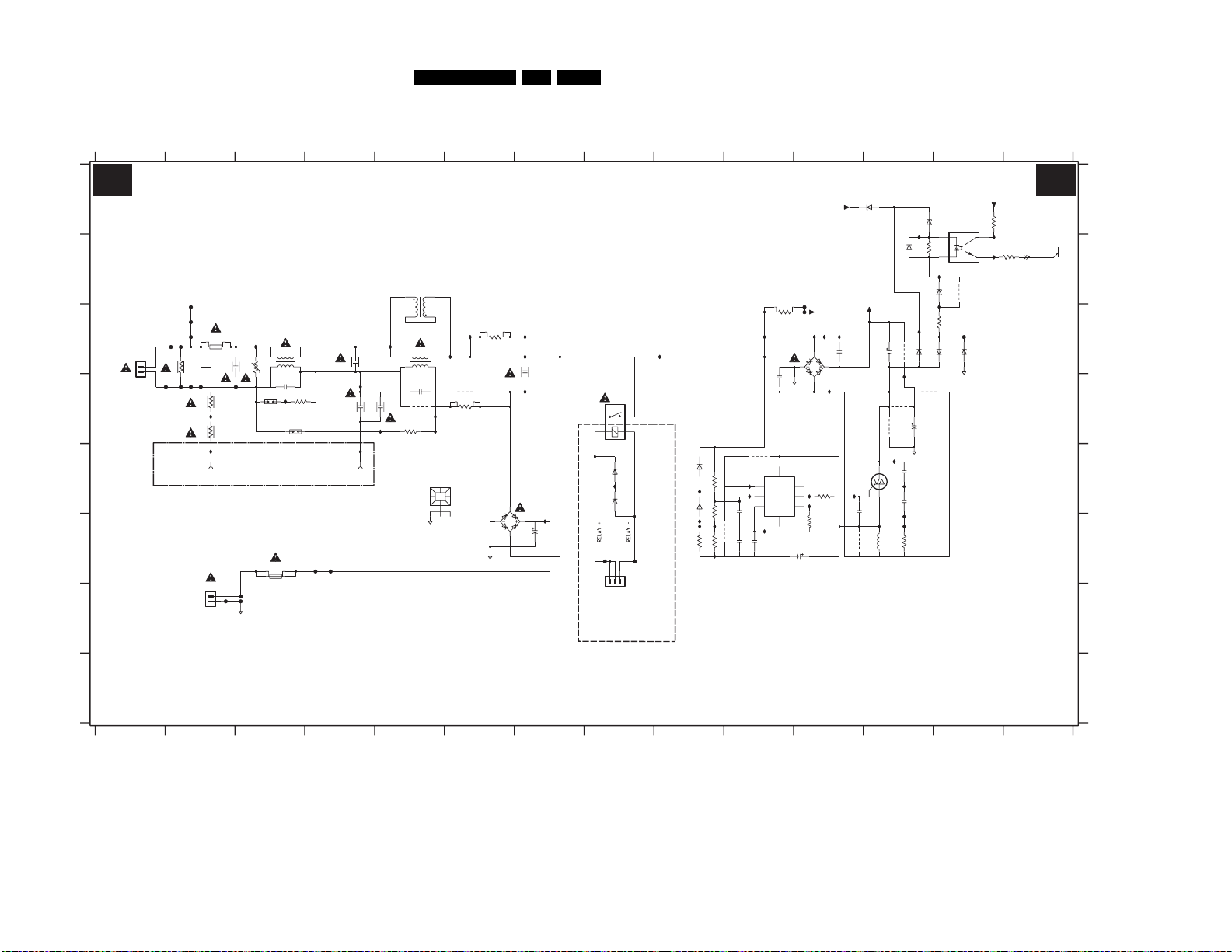
Circuit Diagrams and PWB Layouts
7
. Circuit Diagrams and PWB Layouts
70BJ3.0E LA 7.
Display Supply 32”: Filter & Stby
1 2 3 4 5 6 7 8 9 10 11 12 13 14
MAINS FILTER + STANDBY
A1 A1
A
B
MAINS INPUT
95-264Vac
C
D
E
F
G
H
3104 313 6092.4
400V_HOT
MAINS FILTER
5403
124
3
I442
3450
I444
I411
5402
2 3
1 4
470n
DMF3547HB60
I416
220p
I430
1001
1
2406
47p
*
9003
220p
2409
I455
I818
3404
I432
220R
1011
HEATSINK
1R0
I445
9005
I412
9001
3451
1R0
GNDHOT
DF06M
2408
100n
I415
G5PA-1-5VDC
I424
6506
I456
10u
2503
F420
4V9 (0V)
1305
AUDIO-STANDBY
1450
6461
BAS316
6460
BAS316
3
1
2
TO
I413
HOT GROUND
COLD
GROUND
F421
B3B-EH-A
6809
1N5062
I814
6808
1N5062
I816
I828
I815
22K
3807
I813
9810
7805
AVS1ACP08
I426
1M0
7 6
3800
I427
8
2 3
47n
3806
2805
470R
I428
9806
47n
20K
3804
2802
100p
2811
I820
F422
3810
25V_HOT
12K
F423
I810
6807
GBJ6J
56n
2804
4
VDD
MODE
NC
I423
5
VM
VG
I425
OSIN
OSOUT
VSS
91K
3802
1
2806
50V
47u
F413
F412
2
3401
1
1308
F415
F418
TO
AUDIO-STANDBY
F410
F411
F414
4M7
F416
F419
PTF/65
T4AH 250V
3402
3403
GND screw
1400
I419
I429
1000
1
2400
F417
4M7
4M7
I410
5401
2 3
1 4
3400
470n
DMF3547HB60
V
2404
47p
1403
I431
500V
COLD GROUND
2401
3405
220R
1402
500V
2407
for AP : 220p
for CH, EUR, US : 470p
GND screw
HOT GROUND
T1AE 250V
1401
GNDHOT
PTF/65
F424
F425
1306
1
2
F426
F428
F427
282V (309V)
1 2 3 4 5 6 7 8 9 10 11
6466
BZG03-C200
400V_HOT
I812
I811
56n
2803
I817
3803
390R
7806
I421
47n
2808
I422
9812
5804
300V (0)
2815
33u
I819
9813
9811
I420
AVS10CB
6467
I827
3410
6464
BAS316
I834
I414
330u
9814
6155
BYG10
9808
330u
2816
100n
2810
I825
100n
2809
I824
I826
4R7
3805
12 13 14
BZX384-C33
1
47K
I833
6468
BZX384-C33
22K
3408
6154
BYG10
7807
TCET1102(G)
9818
F429
6465
4
32
BZG03-C200
25V_HOT
3406
I441
10K
I829
3409
1K0
A2
LATCH
G_15970_001.eps
160306
F425 G3
1000 E2
F426 G2
1001 E4
F427 F4
1011 E5
F428 F4
1305 F8
F429 C13
1306 G2
I410 C3
1308 D1
I411 C5
1400 C2
I412 C6
1401 F3
A
I413 C9
1402 D3
I414 C12
1403 D3
I415 D7
1450 D8
I416 D4
2400 C2
I419 D2
2401 C4
I420 E12
2404 D3
I421 E11
2406 D5
I422 F12
2407 D4
I423 E11
2408 C7
I424 E8
2409 D5
I425 E11
2503 F7
I426 E10
2802 F10
B
I427 E10
2803 C11
I428 F10
2804 D10
I429 E2
2805 E10
I430 E4
2806 F11
I431 D3
2808 E11
I432 D5
2809 E12
I441 B13
2810 E12
I442 C6
2811 F10
I444 C7
2815 C12
I445 C7
2816 D12
I455 D5
3400 C3
C
I456 F7
3401 C2
I810 C11
3402 D2
I811 C11
3403 D2
I812 C11
3404 D5
I813 C10
3405 D3
I814 E9
3406 A13
I815 F9
3408 C13
I816 F9
3409 B14
I817 D11
3410 B12
I818 D5
3450 C6
I819 D12
3451 D6
I820 F9
3800 E9
D
I824 F12
3802 F11
I825 E12
3803 E11
I826 F12
3804 F9
I827 A12
3805 F12
I828 F9
3806 E9
I829 B13
3807 F9
I833 B13
3810 C10
I834 C12
5401 C3
5402 C5
5403 B5
5804 F12
6154 C13
E
6155 C12
6460 E8
6461 E8
6464 B12
6465 C13
6466 A12
6467 A12
6468 B13
6506 F6
6807 C11
6808 E9
F
6809 E9
7805 E10
7806 E12
7807 A13
9001 D6
9003 D5
9005 C6
9806 F9
9808 D12
9810 E10
9811 D12
9812 F11
G
9813 D12
9814 C12
9818 B13
F410 B2
F411 C2
F412 C2
F413 C2
F414 C2
F415 D2
F416 D2
F417 D3
F418 D2
H
F419 D2
F420 F8
F421 F8
F422 C11
F423 C11
F424 G3

Circuit Diagrams and PWB Layouts
Display Supply 32”: Supply
1 2 3 4 5 6 7 8 9 10 11 12 13 14
SUPPLY
A2 A2
A
B
C
2040
D
E
F
G
3067
100R
I143
BAS316
6020
H
I
3104 313 6092.4
1
25V_HOT
20V4 (0V)
I103
3002
39K
2K7
560p
3003
2034
27K
3004
2009
3043
10R
3009
I021
3K3
2007
470n
16V
6009
I142
PDZ18-B
470R
I141
3010
2010
100u
6081
BZX384-C22
3000
4R7
470u
2002
I006
I032
I096
5017
50R
I035
BAS316
CONTROL
7001
3005
33K
10K
I010
3058
5M6
400V_HOT
I025
6022
I027
3050
820K
SOFTSTART
CONTROL
I018
*
15n
2027
I022
10K
3066
I013
3027
I135
10n
3047
2019
MC34067P
9
1
2
3
16
6
8
7
11
I105
3053
680K
50V
BC857BW
7017
I023
10K
3064
100K
2026
47R
I134
VS-CONTROLLER
100p
2005
3048
I007
100p
100p
630V
200p
I008
2006
2035
2004
I009
1n0
25V
100p
630V
RES
3006
6001
BAS316
2K7
I104
3007
3008
10K
330R
I029
I028
3011
470R
BZX384-C4V7
2 3 4 5 6 7 8 9 10 11 12 13 14
BAS316
6051
BIAS SUPPLY
18V (0V)
BAS316
2n2
10n
I044
3033
I098
I040
I043
1R0
BYG22D
1m0
2003
9004
5009
I036
2015
50V
10n
*
2018
100n
22R
3045
3075
1K0
I140
7004
BC847BW
I011
3055
I131
220R
I031
6080
9008
*
5
14
OA
12
OB
13
10
FI
68K
1n0
3061
CURRENT
PROTECTION
I024
2008
3070
1K0
3051
6006
I133
BAS316
47n
2046
I137
10K
6079
BYG22D
I012
3065
3013
16V
470n
BC857BW
3071
I095
6077
BYG22D
100K
I033
6011
BAS316
10K
6010
I139
7009
I138
0V (0V)
10K
2077
2047
I132
1n0
2048
6017
BAS316
I097
6082
*
BYG22D
9009
16V (0V)
15
VCC
VREF
EN|UA
OSCC
OSCR
OSCCC
OS
EAO
PGND
Ip
In
SOST
GND
4
2050
I020
15K
3012
7018
BC847BW
50V
2n2
3068
2K2
I136
A1
LATCH
3056
220R
I100
I099
6078
5010
1m0
I101
80R
470p
2063
80R
5015
F003
F004
5016
80R
6005
BAT54 COL
F008
100n16V
2016
I106
3046
3001
100R
6015
BAS316
I296
6014
BZX384-C22
I295
10K
3089
2060
I107
5001
4
3
I108
2
470p
S13932-04
BAT54 COL
2064
6004
F009
I034
2014
2n2
22R
22R
3021
71BJ3.0E LA 7.
3
I114
10n
2011
c001
7002
TCET1102(G)
5002
8 9
7
6
5
3
2
1
BS51
1600V
for EUR, US : 1n5
for CH, AP : 470p
2000
470p
F023
F300
COLD GROUND
11V5 (0V8)
14
2K2
3069
I063
2
10V5 (0V)
0V (0V)
7030
BC847BW
5027
50R
I070
3
I116
5028
I072
50R
I117
10
5025
11
50R
12
I073
13
14
15
16
I076
5026
50R
I123
2290
50V10n
3292
560R
GND_SND
3059
+295V
470K
+24V
COLD GROUND
I062
2039
2028
1n0
STPS20L45CT
2044
1n0
I074
6033
BYV27-600
6031
BYV27-600
2067
100p
I124
*
I005
3032
470n
50V
2
6044
9029
50V
2
6045
STPS20L45CT
2001
I048
50V
2029
1n0
50V
2049
1n0
I041
50V
2045
1n0
I080
21
5AT 250V
1007
STPS8H100FP
STPS8H100FP
I292
50V
1n0
10K
47K
2
I077
372(5.000)
470p
2293
470p
3031
2291
6291
6293
6021
BYV27-600
BYV27-600
50V
50V
3062
22K
6019
I146
1
6018
13
F027
13
2066
100p
6034
6032
F021
DC_PROT
BYV27-200-TAP
9030
2020
BYV27-200-TAP
F028
STPS20H100CT
I290
2292
I291
2294
I293
I047
2054
3063
220K
F022
3999
1K0
100n
9076
BAS316
I148
Vs
Voltage
Adj.
F292
F290
F295
24V-version
6101
3101
15K
PSMN035
2057
22n
7101
3
2
6102
1
BZX384-C12
22n
6103
2059
3103
BZX384-C15
*
15K
1
K
7102
TS2431
R
2
A
3104
3
22n
22n
BAS316
2058
6104
+12V
F019
*
*
56n
2078
9071
9070
2051
220n
2052
220n
2053
220n
2033
220n
I088
6023
2024
220n
BAS316
16V
F014
1%
1K8
3025
I093
470R
*
3034
3026
F296
9075
7021
BSP030
4
2
3
1
1009
HEATSINK
0V (0V)
*
F046
2041
220n
2042
220n
2043
220n
2025
220n
9074
1%
1K0
1M02
B7B-EH-A
1010
HEATSINK
3040
I092
3041
7
6
5
4
3
2
1
F047
+12Vb
F048
9072
*
2n2
2032
8K2
I121
3024
*
15K
3038
I122
33K
9002
TO
AUDIO - SUPPLY
1002
1
GND screw
1M08
1
2
3
4
5
6
B6B-PH-K
1012
HEATSINK
3057
2023
470n
220R
A2
+12V
F016
*
10n
2021
2m2 25V
2031
2055
33K
3052
I119
25V2m2
*
15K
3037
3022
680R
2038
7010
18K
1
BZX384-C15
2068
470n
16V4m7
1
K
A
3
3023
15K
R
A2
F297
VSND_POS
GND_SND
F298
VSND_NEG
+12V
4
2
3
2
9077
8V7 (0V)
2030
I094
DC_PROT
F293
F294
2056
I089
16V
F017
F012
F025
F024
16V4m7
2022
I085
TS2431
3030
5293
3u3
3m3
5291
3u3
3m3
5292
3u3
7020
BSP030
6016
10u 25V
G_15970_002.eps
HOT GROUND
I030
3100
10R
F299
400V_HOT
F018
80R
5007
I001
80R
DRIVE
F002
47R
3015
I037
BC857BW
7007
I004
LOW SIDE
3017
3018
I059
BC857BW
7008
STP15NK50ZFP
6013
SML4744
DRIVE
100R
STP15NK50ZFP
I057
47R
6012
I055
c002
7005
I294
9024
7006
SML4744
5008
I002
F029
80R
5005
1600V
2017
I111
10n
2000V
2013
1n5
50R
5004
I110
F005
FLM 1/6W
5040
80R
80R
5013
I113
I112
2000V
1n5
2012
9025
50R
5041
I064
2061
HIGH SIDE
2n2
I042
3014
I003
2n2
6003
I045
6
7
9
10
I038
6007
BAS316
100R
2072
3035
BAS316
1n0
I046
3K3
6027
3016
BAS316
3K3
I109
3029
3K3
I039
2062
2065
2n2
2n2
6008
6002
I052
BAS316
BAS316
2071
3028
3K3
1n0
6028
3020
I051
3K3
BAS316
3019
I145
3K3
GND3
I081
2000V
I084
HOT GROUND
7009 G5
7010 F12
7017 F3
7018 F4
7020 H12
7021 H13
7030 A10
7101 B13
7102 C14
9002 G14
9004 B6
9008 A4
9009 A4
9024 D8
9025 E8
9029 C11
9030 C11
9070 D13
9071 D13
9072 D14
9073 D14
9074 E13
9075 H13
9076 H12
9077 H12
F002 C8
F003 C6
F004 D6
F005 D9
F008 D6
F009 D7
F012 D12
F014 F13
F016 B12
F017 C12
F018 A8
F019 D13
F021 A11
F022 A12
F023 F9
F024 D12
F025 D12
F027 D11
F028 C11
F029 B9
F046 I13
F047 I13
F048 I13
F290 H13
F292 G13
F293 G12
F294 H12
F295 H13
F296 G13
F297 G12
F298 H12
F299 A9
F300 F9
I001 B9
I002 B9
I003 C7
I004 D8
I005 A11
I006 B3
I007 C3
I008 C3
I009 C2
I010 D3
I011 I5
I012 D4
I013 F3
I018 E3
I020 F4
I021 E2
I022 F3
I023 F3
I024 F4
I025 F3
I027 C3
I028 G2
I029 G3
I030 A9
I031 A4
I032 A3
I033 F5
I034 F7
I035 A3
I036 F6
I037 C8
I038 C8
I039 D7
I040 A5
I041 E11
I042 C8
I043 A6
I044 A6
I045 C7
I046 C8
I047 I12
I048 D11
I051 E8
I052 D8
I055 E8
I057 D8
I059 E8
I062 A11
I063 A10
I064 B7
I070 B10
I072 C10
I073 D10
I074 E11
I076 E10
I077 E11
I080 F11
I081 F7
I084 F9
I085 F12
I088 E13
I089 F12
I092 F13
I093 F13
I094 G12
I095 A5
I096 A3
I097 A4
I098 A5
I099 A6
I100 A7
I101 A7
I103 C1
I104 D2
I105 E3
I106 E6
I107 C7
I108 D6
I109 C8
I110 D9
I111 C9
I112 E9
I113 E9
I114 D9
I116 C10
I117 C10
I119 C12
I121 F14
I122 F14
I123 F10
I124 G11
I131 I6
I132 I5
I133 I4
I134 I3
I135 G3
I136 H4
I137 G4
I138 H5
I139 G5
I140 G5
I141 H2
I142 H1
I143 G1
I145 E8
I146 B11
I148 B13
I149 D14
I152 B14
I290 G11
I291 G11
I292 H11
I293 H11
I294 C8
I295 H6
I296 G6
c001 I9
c002 E8
3032 B11
1002 H14
3033 A5
1007 G11
3034 G13
1009 I13
3035 C7
1010 I14
1012 I14
3037 C12
1M02 G13
3038 F14
3040 F13
1M08 H14
3041 G13
2000 E10
2001 D11
3043 D2
2002 A2
3045 G5
2003 A5
3046 F6
A
2004 C2
3047 H3
2005 D2
3048 D2
2006 C2
3050 E3
2007 E2
3051 H4
3052 C12
2008 G4
3053 E4
2009 D2
3055 I5
2010 H1
+24V
2036
100n
3102
*
22K
220n
I152
33K
2K7
3105
+295V
+12V
9073
I149
*
3060
100R
15K
160306
B
C
D
E
F
G
H
I
2011 E9
2012 E9
2013 C9
2014 F7
2015 F5
2016 E6
2017 C9
2018 F5
2019 H3
2020 C11
2021 B12
2022 E12
2023 A12
2024 F13
2025 E13
2026 G3
2027 F3
2028 B11
2029 D11
2030 F12
2031 B12
2032 E14
2033 E13
2034 C2
2035 C2
2036 B14
2038 E12
2039 B11
2040 C1
2041 D13
2042 E13
2043 E13
2044 C11
2045 E11
2046 I4
2047 I5
2048 I5
2049 E11
2050 E4
2051 D13
2052 E13
2053 E13
2054 I11
2055 C12
2056 C12
2057 B13
2058 B13
2059 B14
2060 C7
2061 B7
2062 D7
2063 C6
2064 D6
2065 D8
2066 E11
2067 F11
2068 I12
2071 E8
2072 C8
2077 H5
2078 D13
2290 G10
2291 G11
2292 G11
2293 H11
2294 H11
3000 A3
3001 F6
3002 C2
3003 C1
3004 D2
3005 C3
3006 D3
3007 E2
3008 E2
3009 E2
3010 H2
3011 H2
3012 F4
3013 F4
3014 C8
3015 C8
3016 C7
3017 D8
3018 E8
3019 E7
3020 E7
3021 G7
3022 C12
3023 F12
3024 F14
3025 F13
3026 G13
3027 G3
3028 E7
3029 C7
3030 G12
3031 A11
3056 I4
3057 A12
3058 E3
3059 H11
3060 E14
3061 E4
3062 I11
3063 I11
3064 F3
3065 E4
3066 F3
3067 G1
3068 G4
3069 A10
3070 H4
3071 H4
3075 G5
3089 H6
3100 A9
3101 A13
3102 B14
3103 B14
3104 C14
3105 C14
3292 G10
3999 A12
5001 C7
5002 C9
5004 D9
5005 C9
5007 B9
5008 B9
5009 B6
5010 A6
5013 E9
5015 C6
5016 D6
5017 A3
5025 D10
5026 E10
5027 B10
5028 C10
5040 D9
5041 E9
5291 G12
5292 H12
5293 G12
6001 D2
6002 D8
6003 C7
6004 D6
6005 D6
6006 I4
6007 C7
6008 D7
6009 H2
6010 G5
6011 F5
6012 E8
6013 C8
6014 H6
6015 G6
6016 I12
6017 I5
6018 C11
6019 B11
6020 H1
6021 D11
6022 H3
6023 F13
6027 C8
6028 E8
6031 F11
6032 F11
6033 E11
6034 E11
6044 B11
6045 C11
6051 H4
6077 A5
6078 A6
6079 A4
6080 A4
6081 A2
6082 A4
6101 A13
6102 B14
6103 B13
6104 C13
6291 G11
6293 H11
7001 C4
7002 A10
7004 H5
7005 C8
7006 D8
7007 C8
7008 E8
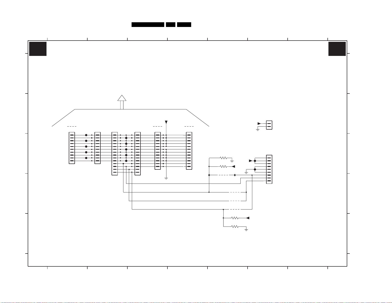
Circuit Diagrams and PWB Layouts
72BJ3.0E LA 7.
Display Supply 32”: Connections
1
A3 A3
CONNECTIONS
A
2 3 4 5 6 7
TO
DISPLAY
B
9052
*
1314
*
1
2
3
4
5
6
C
7
8
9
10
B10P-PH-K-S
F030
F031
F032
F033
F034
B10P-PH-K-S
1315
1321
*
1
2
3
4
5
6
7
8
9
10
1
2
3
4
5
6
7
8
9
10
11
12
13
14
B14B-PH-K
*
F035
F036
F037
F038
F039
B14B-PH-K
1319
*
1
2
3
4
5
6
7
8
9
10
11
12
13
14
1316
1
2
3
4
5
6
7
8
9
10
11
12
B12P-PH-K
+24V
+12Vb
+12V
+295V
F043
F044
*9053
*
9051
B12P-PH-K
*
*1317
1
2
3
4
5
6
7
8
9
10
11
12
I702
3902
3903
10K
10K
9057
*
*
I701
LAMP-ON-OFF
*
1310
1
2
B2P-VA-BF-RD
1M64
B9B-PH-K
1
2
3
4
5
6
7
8
9
TO
DISPLAY
TO
AUDIO-STANDBY
A
B
C
1310 B6
1314 B1
1315 B2
1316 B3
1317 B4
1319 B3
1321 B2
1M64 C6
3902 C5
3903 C5
3904 E5
3905 E5
9051 B4
9052 B1
9053 B3
9054 D5
9055 D5
9056 D5
9057 D5
F030 C2
F031 C2
F032 C2
F033 C2
F034 C2
F035 C3
F036 C3
F037 C3
F038 C3
F039 C3
F043 C6
F044 C6
I701 C5
I702 C4
D
E
3104 313 6092.4
BOOST
DIM-CONTROL_PWM
SELECT-PWM-ANA
9055
9054
3904
3905
9056
10K
10K
*
*
*
+12Vb
*
1 2 3 4 5 6 7
G_15970_003.eps
160306
D
E

Circuit Diagrams and PWB Layouts
G_15970_004.eps
160306
3104 313 6092.4
1000 A1
1001 A3
1002 A11
1007 A10
1009 B9
1010 C9
1011 C3
1012 A9
1305 A3
1306 A4
1308 C1
1310 A10
1314 C11
1315 A11
1316 A11
1317 C11
1319 A11
1321 C11
1400 C1
1401 A4
1402 A2
1403 B1
1450 A3
1M02 B11
1M08 C11
1M64 A9
2000 A7
2002 A7
2003 A6
2004 A6
2005 A6
2010 A7
2011 B7
2012 C7
2013 C6
2014 A7
2017 B6
2020 C8
2021 C8
2022 A8
2032 A8
2038 A9
2054 C10
2066 B9
2067 B10
2078 A10
2292 A11
2294 A11
2400 C2
2401 B1
2404 B1
2406 A3
2407 A3
2408 B3
2409 A3
2503 A4
2803 B3
2804 B4
2806 B4
2809 C4
2810 C4
2815 A3
2816 A5
3000 A5
3014 B6
3015 C5
3017 C7
3018 C6
3024 A9
3026 A10
3033 A6
3038 A9
3050 A5
3053 A5
3058 A5
3059 A11
3060 A11
3400 C2
3401 C2
3402 A1
3403 A1
3404 A2
3405 B1
3408 A5
3450 A2
3451 A2
3800 A4
3805 C4
3807 B4
3810 A4
5001 B6
5002 A8
5004 C6
5005 C6
5007 B6
5008 C5
5009 B7
5010 B6
5013 C7
5015 A6
5016 A6
5017 A5
5025 B9
5026 A9
5027 C9
5028 C10
5040 B6
5041 C7
5291 B11
5292 C11
5293 A11
5401 B2
5402 A1
5403 A3
5804 B4
6018 C10
6019 C10
6021 B9
6031 B10
6032 B10
6033 B9
6034 B9
6044 C9
6045 C10
6291 A9
6293 A10
6506 A3
6807 C3
6808 A4
6809 A4
7001 A6
7002 A7
7005 C6
7006 C7
7101 B10
7805 B4
7806 C4
7807 A5
9001 A3
9003 A3
9004 A7
9005 B3
9006 B10
9007 A8
9011 A8
9012 C8
9013 B8
9014 B1
9015 A5
9016 A7
9017 A5
9018 A6
9019 A6
9020 B7
9021 A6
9022 C3
9023 C3
9024 C6
9025 B7
9027 B9
9029 C9
9030 C10
9031 A9
9032 A9
9033 A9
9034 A10
9035 B8
9037 B9
9038 A9
9040 A9
9051 C11
9052 C11
9053 A11
9070 A10
9075 C10
9080 A7
9081 C2
9086 B11
9087 B9
9088 A10
9090 A9
9092 A7
9093 A7
9098 B3
9100 A11
9101 B9
9102 B10
9104 B10
9105 B10
9808 B4
9811 B5
9812 C4
9813 B5
9814 A5
9901 A10
9902 A11
9903 C9
Layout Display Supply 32” (Top Side)
73BJ3.0E LA 7.

Circuit Diagrams and PWB Layouts
74BJ3.0E LA 7.
Layout Display Supply 32” (Overview Bottom Side)
2018 A6
2001 B3
2019 A6
2006 A6
2007 A7
2023 A2
2008 A6
2024 B2
2025 A2
2009 A6
2026 A7
2015 A6
2027 A7
2016 A6
2028 C3
2029 B3
2030 B2
2031 A2
2033 A2
2034 A6
2035 A6
2036 B2
2039 B2
2040 A6
2041 A2
2042 A2
2043 A2
2044 C2
2045 B2
2046 A5
2047 A6
2048 A6
2049 B2
2050 A6
2051 A2
2052 A2
2053 A2
2055 B3
2056 B3
2057 B3
2058 B2
2059 B2
2060 C7
2061 B6
2062 C6
2063 A6
2064 A6
2065 C5
2068 C2
2071 C5
2072 C6
2077 A5
2290 B4
2291 A3
2293 A2
2802 B8
Part 1
G_15970_005a.eps
3104 313 6092.4
2805 B8
2808 C8
2811 B8
3001 A5
3002 A6
3003 A6
3004 A6
3005 A6
3006 A6
3007 A7
3008 A7
3009 A7
3010 A5
3011 A6
3012 A6
3013 A6
3016 C7
3019 C5
3020 C5
3021 A5
3022 B2
3023 B2
3025 B2
3027 A7
3028 C5
3029 C7
3030 B2
3031 B2
3032 B1
3034 B2
3035 C7
3037 A2
3040 B2
3041 B2
3043 A6
3045 A6
3046 A5
3047 A5
3048 A6
3051 A5
3052 A2
3055 A5
3056 A5
3057 A2
3061 A6
3062 C2
3063 C2
3064 A6
3065 A7
3066 A6
3067 A5
3068 A5
3069 A4
3070 A5
3071 A5
3075 A5
3089 A5
3100 A5
3101 B2
3102 B2
3103 B2
3104 B2
3105 B2
3292 B4
3406 A7
3409 A7
3410 A7
3802 B8
3803 B7
3804 B8
3806 B8
3902 A1
3903 C1
3904 C1
3905 A1
3999 B9
6001 A6
6009 A5
6002 C5
6010 A6
6003 C7
6011 A6
6004 A6
6012 B5
6005 A6
6013 B6
6006 A6
6014 A5
6007 B7
6015 A5
6008 C6
G_15970_005b.eps
6016 C2
6017 A6
6020 A5
6022 A6
6023 A2
6027 C7
6028 C5
Part 2
6051 A5
6077 A5
6078 B6
6079 A6
6080 A7
6081 A5
6082 A7
6101 B3
6102 B2
6103 B2
6104 B3
6154 A7
6155 A7
6460 A9
6461 A9
6464 A7
6465 A7
6466 A7
6467 A7
6468 A7
7004 A5
7007 C6
7008 C5
7009 A5
7010 A2
7017 A6
7018 A6
7020 C2
7021 C2
7030 B2
7102 B2
9002 A2
9008 A7
9009 A7
9026 A2
9054 A1
9055 A1
9056 A1
9057 A1
9060 A5
9071 A2
9072 A1
9073 A2
9074 A2
9076 C2
9077 C2
9085 B2
9110 C2
9806 B8
9810 B8
9818 A7
G_15970_005.eps
160306
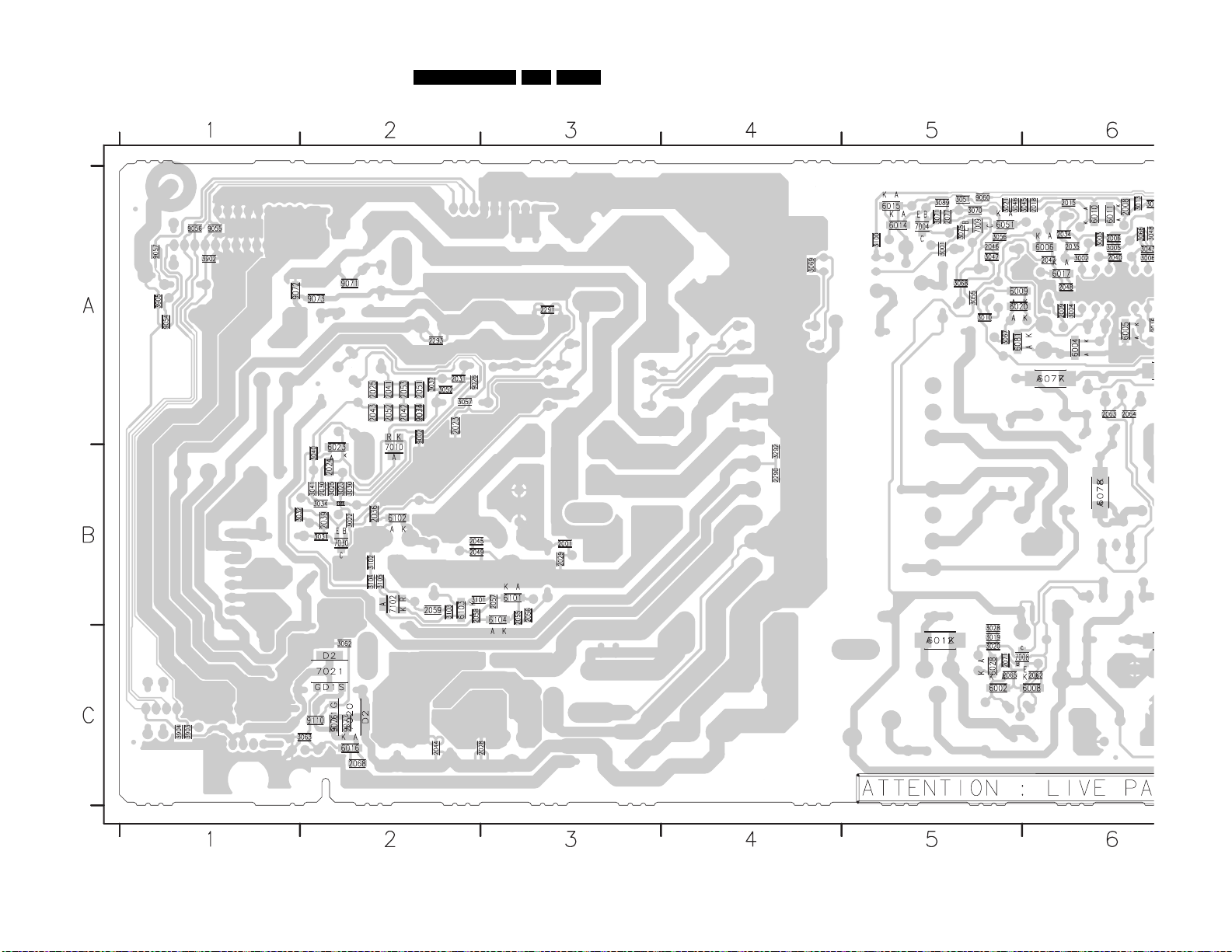
Circuit Diagrams and PWB Layouts
G_15970_005a.eps
160306
Part 1
Layout Display Supply 32” (Part 1 Bottom Side)
75BJ3.0E LA 7.
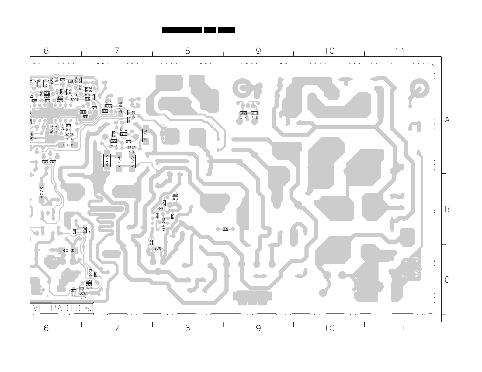
Circuit Diagrams and PWB Layouts
G_15970_005b.eps
160306
Part 2
Layout Display Supply 32” (Part 2 Bottom Side)
76BJ3.0E LA 7.

Circuit Diagrams and PWB Layouts
77BJ3.0E LA 7.
Display Supply 37”: Part 1
1 2
DISPLAY SUPPLY: PART1
A1 A1
3 4 5 6 7
A
1011
HEATSINK
2401
2407
GND-SCR
GND-SCR
9062
I446
I430
+24V_+295V
470n
220p
9073
MAINS FILTER
I411
I416
I455
3404
220R
F020
F031
F032
I459
10K
6056
BZX384-C3V3
5403
124
5402
2 3
1 4
DMF3547HB60
2406
47p
9003
1317
B12P-PH-K
3432
10K
3433
3
1
2
3
4
5
6
To Display
7
8
9
10
11
12
3450
I442
I412
I414
I432
DIM-CONTROL
+12Vd
I444
1R0
I445
9005
100n
2408
I415
9001
3451
1R0
HOT GROUND
COLD GROUND
+5V-SW
RELAY-
10K
3422
7801
I436
BC817-25W
10K
3423
3424
220R
I437
7802
BC847BW
3413
ON-OFF
BOOST
B
C
D
E
F
G
H
MAINS INPUT
95-264Vac
F411
F410
2
1
1308
1314
1
F040
2
3
4
F015
5
6
7
8
9
10
B10P-PH-K-S
F414
PTF/65
T5AH 250V
4M7
3401
F415
F416
F418
F001
F006
F010
F011
F013
B10P-PH-K-S
+12Vd
F419
1315
3402
3403
GND-SCR
GND-SCR
1
2
3
4
5
6
7
8
9
10
3430
10K
2400
470n
3400
F417
4M7
I419
4M7
9043
1320
1
2
3
4
5
6
7
8
9
10
11
12
13
14
B14B-PH-K
10K
6055
3431
BZX384-C3V3
I443
9015
2
5405
V
1
9046
1403
500V
1404
V_NOM
1402
500V
1405
V_NOM
I458
I457
3
4
DMF2405H60
I429
B14B-PH-K
9070
9071
5401
2 3
1 4
2403
22n
DMF3547HB60
2404
47p
9042
3405
I431
220R
1319
9045
1316
1
1
2
2
3
3
4
4
5
5
6
6
7
7
8
8
9
9
10
10
11
11
12
12
13
B12P-PH-K
14
9072
I410
1400
F413
F412
3104 313 6121.3
1 2
3 4 5 6 7 8 9 10 11 12 13 14
8 9 10 11 12 13 14
DC+DC-
400V_HOT
33u
5404
9817
+5V-SW
I814
I816
I815
6809
6808
3807
I820
6462
1N5062
1N5062
1M0
3800
1N5062
3806
470R
I828
20K
22K
3804
+24V_+295V
9819
I433
9815
I434
2805
9806
2807
3077
47K
3078
1K0
POWER-GOOD
I813
9810
7805
AVS1ACP08
I426
7 6
MODE
I427
VM
2 3
OSIN
47n
I456
I428
47n
100p
2802
BAS316
F034
F422
3810
25V_HOT
12K
F423
6807
GBJ6J
56n
2804
4
VDD
NC
I423
58
VG
I425
OSOUT
VSS
3802
1
2806
50V47u
6083
6024
I026
3076
7013
BC847BW
2409
I810
I031
I811
3803
390R
91K
BZX384-C22
8K2
3074
1K0
BC847BW
10n
400V_HOT
I812
56n
2803
I817
2816
I421
2808
9812
I032
I035
7014
I435
6463
VAC-L
VAC-N
1450
G5PA-1-5VDC
4V8 (0V)
6461
BAS316
RELAY +
F420
I424
6460
BAS316
+12Vd
9816
6469
3425
I439
10K
BZX384-C2V7
2n2
9820
PLT09H
F026
9821
F019
I438
15K
2402
1N5062
I413
RELAY -
F421
I440
STANDBY
1M08
1
2
5406
3
4
5
6
B6B-PH-K
I830
6467
6466
I827
BZG03-C200
400V_HOT
3410
6464
BAS316
6155
BYG10
2815
I418
330u
330u
5804
BZX384-C18
6K8
2K2
9808
9813
9811
I420
2810
100n
I825
AVS10CB
100n
2809
I824
I826
33u
4R7
3805
ON-OFF
DIM-CONTROL
+24V_+295V
9814
I417
7806
47n
I422
6026
I019
3073
3072
BZX384-C33
47K
RES
TCET1102(G)
I833
BZX384-C33
I834
22K
3408
6154
B2P-VA-BF
6468
BYG10
25V_HOT
10K
3406
I829
7807
I441
0v(0v)
9818
F424
6465
BZG03-C200
+5V-SW
9054
9052
F033
I460
I461
B6B-PH-K
9041
9053
1310
1
2
LATCH
1318
1
2
3
4
5
6
c003
GND-SSP
G_15970_006.eps
160306
1308 C1
1310 H13
1314 F1
1315 F2
1316 F4
1317 F5
1318 G14
1319 F3
1320 F3
1400 C2
1402 D3
1403 D3
A
1404 D3
1405 D3
1450 D8
1M08 H9
2400 C2
2401 C4
2402 G7
2403 C3
2404 C4
2406 C5
2407 E4
B
2408 C7
2409 H11
2802 F10
2803 C11
2804 C10
2805 E10
2806 F11
2807 F10
2808 E12
2809 E12
2810 E12
C
2815 C12
2816 D12
3072 H12
3073 G12
3074 H11
3076 G11
3077 G10
3078 G10
3400 C3
3401 C1
3402 D2
D
3403 E2
3404 D5
3405 D4
3406 A13
3408 C13
3410 B13
3413 G7
3422 F7
3423 F7
3424 F7
E
3425 F8
3430 H2
3431 H3
3432 H5
3433 H5
3450 C6
3451 D6
3800 E10
3802 E11
3803 E11
3804 F10
F
3805 F12
3806 E10
3807 F9
3810 B10
5401 C4
5402 C5
5403 B5
5404 A9
5405 C3
5406 H8
5804 F12
G
6024 G11
6026 G12
6055 H2
6056 H5
6083 G10
6154 C13
6155 C12
6460 E8
6461 E8
6462 B9
6463 B9
6464 B12
H
6465 C13
6466 A12
6467 A13
6468 B13
6469 F8
6807 C11
6808 E9
6809 E9
7013 H11
7802 G7
7805 E10
7806 E12
7807 A13
9001 C6
9003 D5
9005 C6
9015 C3
9041 H13
9042 D4
9043 F3
9045 F4
9046 C3
9052 G13
9053 H13
9054 G13
9062 C4
9070 H3
9071 H3
9072 H4
9073 H5
9806 E10
9808 C12
9810 D10
9811 D12
9812 F12
9813 D12
9814 C12
9815 B10
9816 F8
9817 B9
9818 B13
9819 A10
9820 H8
9821 H8
F001 F1
F006 G1
F010 G1
F011 G1
F013 G1
F015 G1
F019 H8
F020 F5
F026 H8
F031 G5
F032 G5
F033 G14
F034 H10
F040 G1
F410 C1
F411 C1
F412 C1
F413 C2
F414 C2
F415 C1
F416 C2
F417 C2
F418 C2
F419 C2
F420 E8
F421 F8
F422 B11
F423 B11
F424 C13
I019 G12
I026 G11
I031 G11
I032 H11
I035 H12
I410 C2
I411 C5
I412 C6
I413 C9
I414 D6
I415 C7
I416 C5
I417 D12
I418 C12
I419 D2
I420 D12
I421 E11
I422 E12
I423 E11
I424 E8
I425 E11
I426 E10
I427 E10
I428 E10
I429 C3
I430 E5
I431 D4
I432 D6
I433 B10
I434 B10
I435 B9
I436 F7
I437 F7
I439 F8
I440 F8
I441 B13
I442 C6
I443 C3
I444 C7
I445 C7
I446 D5
I455 D5
I456 E10
I457 H3
I458 G3
I459 G5
I460 G14
I461 G13
I810 C11
I811 C11
I812 C11
I813 C10
I814 E9
I815 E9
I816 E9
I817 D11
I820 F9
I824 E12
I825 E12
I826 E12
I827 A12
I828 E9
I829 A14
I830 A12
I833 B13
I834 B13
c003 H14
I438 F7
7014 H11
1011 A7
7801 F7

Circuit Diagrams and PWB Layouts
78BJ3.0E LA 7.
Display Supply 37”: Part 2
1 2 3 4 5 6 7 8 9
DISPLAY SUPPLY: PART2
A2 A2
25V_HOT
A
20V4 (0V)
B
I103
C
D
E
3002
39K
2K7
560p
2040
3003
2034
27K
3004
2009
3043
10R
3009
I021
3K3
2007
470n
16V
F
G
3067
100R
I143
H
BAS316
6009
I142
6020
PDZ18-B
470R
I141
3010
2010
100u
I
3000
4R7
6081
470u
2002
BZX384-C22
I006
VS-CONTROLLER
I007
100p
100p
630V
200p
I008
2006
2004
2035
I009
25V
1n0
100p
100p
630V
2005
RES
3006
6001
BAS316
I010
2K7
3048
I104
3008
3007
330R
10K
400V_HOT
I029
I028
3011
6022
470R
BZX384-C4V7
I096
I048
3005
33K
10K
3058
5M6
I022
I025
2019
5017
50R
CONTROL
I027
288V(0V)
I105
3050
820K
SOFTSTART
CONTROL
I018
50V
15n
2027
RES
10K
3066
F007
3027
100K
I135
10n
47R
3047
I134
I047
MC34067P
BC857BW
7017
I023
3064
2026
BAS316
7001
9
1
2
3
16
6
8
7
11
3053
680K
10K
BAS316
BIAS SUPPLY
16V
470n
BC857BW
22V(0V)
I095
6079
I012
3065
100K
BYG22D
3033
6077
I053
I098
I050
I049
1R0
BYG22D
1m0
2003
9004
5009
I106
I100
I099
6078
5010
1m0
I101
80R
I064
2061
2n2
I003
I107
S13932-04
BAT54 COL
6007
BAS316
2n2
6003
2060
3035
BAS316
I045
3016
5001
3K3
6
3029
3K3
7
I039
9
6008
10
BAS316
3028
3K3
3020
3K3
3019
3K3
470p
2063
80R
5015
F003
4
F004
3
5016
I108
2
80R
6005
470p
2064
6004
BAT54 COL
F009
F008
100n16V
2016
3100
HIGH SIDE
DRIVE
I042
3014
I038
F002
100R
2072
3015
1n0
I046
3K3
6027
I037
BAS316
I109
BC857BW
7007
2062
2065
I004
2n2
2n2
6002
I052
BAS316
3017
3018
2071
1n0
6028
I051
BAS316
I145
GND3
I034
I033
6011
BAS316
6010
10K
3013
I139
7009
I138
10K
3071
2077
2047
I132
10n
1n0
2048
6017
BAS316
BAS316
2n2
I036
2015
50V
10n
RES2018
22R
3045
3075
1K0
I140
7004
BC847BW
I011
3055
220R
22R
3046
3001
100R
100n
6015
BAS316
I296
6014
BZX384-C22
I295
10K
3089
I131
I081
2014
2n2
2000V
22R
3021
RES
I097
I044
6080
6082
BYG22D
BYG22D
9008
RES
9009
15
5
VCC
VREF
EN|UA
OSCC
OSCR
14
OSCCC
OA
OS
12
OB
EAO
13
Ip
PGND
10
FI
In
SOST
GND
4
68K
1n0
3061
2050
I020
6051
CURRENT
PROTECTION
15K
3012
I024
7018
BC847BW
50V
2008
2n2
LATCH
10K
3060
3068
I137
2K2
3070
I136
1K0
6006
3056
I133
220R
BAS316
47n
2046
3104 313 6121.3
I043
10R
400V_HOT
F018
7005
STP15NK50ZFP
47R
6013
BZG05C15
I294
9024
LOW SIDE
DRIVE
7006
100R
STP15NK50ZFP
I057
47R
6012
BZG05C15
I059
BC857BW
7008
9025
I055
c002
HOT GROUND
F299
80R
5007
I001
80R
5008
I002
80R
I111
2013
50R
5004
I110
F005
FLM 1/6W
5013
I113
I112
2012
50R
5041
3 2
F029
5005
1600V
15n
2000V
2017
1n5
7
6
5
5040
3
80R
I114
2
80R
1
2000V
1n5
15n
2011
I084
c001
HOT GROUND
7002
TCET1102(G)
5002
8
BS51
1600V
F023
F300
2000
470p
1 2 3 4 5 6 7 8 9 10 11 12 13
10 11 12 13
COLD GROUND
11V3 (0V)
14
2K2
3069
I063
10V2 (0V)
7030
BC847BW
5027
I070
50R
3
I116
5028
I072
50R
I117
9
5025
10
50R
I073
11
12
13
14
5026
15
50R
16
I076
1009
HEATSINK
HEATSINK
COLD GROUND
9055
2044
1010
0V (0V)
2028
1n0
1n0
BYV27-600
BYV27-600
I062
I005
2039
470n
50V
6044
STPS20L45CT
50V
6045
STPS20L45CT
2029
1n0
I074
2045
1n0
I077
6033
6031
2067
100p
47K
3032
2
1
I150
2
13
I056
50V
3
9056
I054
50V
BYV27-600
BYV27-600
F021
6019
9006
6018
F027
2001
1n0
50V
6021
STPS20H100CT
2049
1n0
50V
6025
STPS20H100CT
2066
100p
6034
6032
3999
1K0
BYV27-200-TAP
25V
2m2
2020
BYV27-200-TAP
F028
F017
F012
2
2
GND screw
F022
3057
220R
2023
470n
F016
+12Vd
10n
RES
2031
2021
2m2 25V
33K
3052
I119
RES
15K
3037
3022
680R
I120
24V4 (0V)
F025
F024
16V4m7
2038
1
I151
2022
16V4m7
9058
13
3023
15K
I085
13V4
7010
1
TS2431
K
A
3
18K
3030
I094
1002
I013
+12Vd
3059
2K2
3036
2036
100K
I014
33K
3049
6030
3044
I015
I017
2037
3025
470R
BC847BW
470n
1%
470R
3026
BAS316
1K8
7031
3042
12K
6023
I093
3034
ONLY FOR
32" SHARP
+12Vd
I152
2051
220n
2052
220n
2053
220n
2033
220n
I088
2K2
1%
3039
F030
9060
2025
220n
8K2
3040
I092
33K
3041
9002
I016
BAS316
3051
4K7
4K7
3054
I089
2024
220n
16V
F014
R
2
16V
100n
2030
Vs
Voltage
Adj.
470n
6054
BZX384-C10
1K0
I041
+24V_+295V
2041
9061
220n
2042
220n
2043
220n
2032
I121
3038
+12Vd
9050
3079
G_15970_007.eps
RES
2n2
3024
RES
220K
I122
+24V_+295V
9057
680R
160306
15K
MRS25 1%
F016 B11
1002 H11
3051 B12
1009 G10
3052 C11
1010 G10
3053 E3
2000 E9
3054 B12
2001 D11
3055 I5
2002 A2
3056 I3
2003 A5
3057 A11
2004 C2
3058 E2
2005 D1
3059 A13
2006 C2
3060 G4
2007 E1
3061 E4
2008 G4
3064 F3
2009 D1
3065 E4
A
2010 H1
3066 F2
2011 E9
3067 H1
2012 E8
3068 H3
2013 C8
3069 A10
2014 F6
3070 H4
2015 F5
3071 H4
2016 E6
3075 G5
2017 C9
3079 G13
2018 F5
3089 H5
2019 H2
3100 A8
2020 C11
3999 A11
2021 C11
5001 C6
2022 E12
5002 D9
B
2023 A12
5004 D8
2024 E12
5005 C8
2025 E13
5007 B8
2026 G3
5008 B8
2027 F2
5009 B5
2028 B10
5010 A6
2029 D10
5013 E8
2030 F12
5015 C6
5016 D6
2031 B12
5017 A3
2032 E13
5025 D10
2033 E13
C
5026 D10
2034 C1
5027 B10
2035 C1
5028 C10
2036 A13
2037 B12
5040 D9
5041 E8
2038 D12
6001 D2
2039 B10
6002 D7
2040 C1
6003 C7
2041 D13
6004 D6
2042 D13
6005 D6
2043 D13
6006 I4
2044 C10
6007 C7
2045 E10
D
6008 D7
2046 I3
6009 H1
2047 I5
6010 G4
2048 I4
6011 F4
2049 E11
6012 E8
2050 E3
6013 C8
2051 D13
2052 D13
6014 H5
2053 D13
6015 G5
2060 C6
6017 I4
6018 C11
2061 B7
6019 B11
2062 D7
6020 H1
2063 C6
E
6021 D11
2064 D6
2065 D7
6022 H2
2066 E11
6023 E13
2067 F10
6025 E11
2071 E7
6027 C7
2072 C7
6028 E7
2077 H4
6030 A12
3000 A2
6031 F10
6032 F11
3001 F5
6033 E10
3002 C1
6034 E11
3003 C1
F
6044 B10
3004 D1
6045 C10
3005 C2
3006 D2
6051 H3
3007 E2
6054 A13
6077 A4
3008 E2
6078 A5
3009 E1
6079 A4
3010 H1
6080 A4
3011 H2
6081 A1
3012 F3
6082 A3
3013 G4
7001 C3
3014 C7
7002 A9
3015 C7
G
3016 C7
7004 H5
3017 D7
7005 C8
3018 E7
7006 D8
3019 E7
7007 C7
3020 E7
7008 E8
3021 G6
7009 H4
3022 C11
7010 E12
3023 E12
7017 F3
3024 E13
7018 F3
3025 F12
7030 A10
3026 G13
7031 B13
3027 G3
9002 G13
H
3028 E7
9004 B5
9006 C11
3029 C7
9008 A3
3030 F11
9009 A3
3032 B10
9024 D8
3033 A5
9025 E8
3034 F13
3035 C7
9050 G13
3036 A13
9055 C10
3037 C12
9056 D10
3038 F13
9057 G13
3039 A13
9058 E11
I
9060 D13
3040 E13
9061 D13
3041 F13
F002 C8
3042 B13
F003 C6
3043 D1
F004 D6
3044 A13
F005 D8
3045 G5
F007 F3
3046 F6
F008 D6
3047 H3
F009 D6
3048 D1
F012 D11
3049 A12
F014 F12
3050 E3
F017 D11
F018 B8
F021 A11
F022 A11
F023 F9
F024 D11
F025 D11
F027 D11
F028 C11
F029 C9
F030 C13
F299 A8
F300 F9
I001 B8
I002 B8
I003 C7
I004 D7
I005 A10
I006 B2
I007 C2
I008 C2
I009 C2
I010 D2
I011 I5
I012 D4
I013 A13
I014 A13
I015 A13
I016 A12
I017 B12
I018 E3
I020 F3
I021 E1
I022 F2
I023 F3
I024 F4
I025 F2
I027 C2
I028 G2
I029 G2
I033 F4
I034 F6
I036 F5
I037 C8
I038 C7
I039 D7
I041 B13
I042 C7
I043 A8
I044 A4
I045 C7
I046 C7
I047 A3
I048 A2
I049 A5
I050 A5
I051 E7
I052 D7
I053 A5
I054 D11
I055 E8
I056 D11
I057 D8
I059 E8
I062 A10
I063 A10
I064 B7
I070 B10
I072 C10
I073 D10
I074 D10
I076 E10
I077 E10
I081 F7
I084 F9
I085 E11
I088 E13
I089 E12
I092 F13
I093 F13
I094 G12
I095 A4
I096 A2
I097 A3
I098 A5
I099 A6
I100 A6
I101 A6
I103 C1
I104 D2
I105 E3
I106 E5
I107 C6
I108 D6
I109 C7
I110 D8
I111 C8
I112 E8
I113 E8
I114 D9
I116 C9
I117 C10
I119 C12
I120 C11
I121 E13
I122 F13
I131 I5
I132 I4
I133 I4
I134 I3
I135 H2
I136 H3
I137 H4
I138 H4
I139 G4
I140 H5
I141 H1
I142 H1
I143 H1
I145 E7
I150 C11
I151 D11
I152 D13
I294 C8
I295 H6
I296 H6
c001 G9
c002 E8

Circuit Diagrams and PWB Layouts
79BJ3.0E LA 7.
Platform Supply 37”: Auxiliary Supply
0P01 G10
1M02 G3
1M03 G3
1M10 H13
1M18 H13
1M46 G15
1M63 G10
1P00 G4
1P01 G4
1P03 A3
1P05 H7
1P06 A1
2P10 B2
2P11 G6
2P12 F12
2P13 E15
2P14 B5
2P15 B7
2P16 B4
2P17 B3
2P18 B6
2P19 B6
2P20 B7
2P21 A1
2P22 A14
2P23 F14
2P24 F15
2P25 B11
2P26 A13
2P27 B11
2P28 B12
2P29 B11
2P30 B12
2P31 D13
2P32 E2
5
2P33 H6
2P34 C15
2P35 A11
2P36 D1
2P37 B14
2P40 E11
2P41 F12
2P42 C11
2P43 C11
2P45 F3
2P47 C12
2P48 D15
2P49 C12
2P50 D15
2P51 A1
2P52 B5
2P53 A12
2P54 E2
2P55 D14
2P56 F12
2P57 F11
2P64 B11
2P80 E10
3P00 B12
3P01 B12
3P02 B12
2
3P03 B12
3P04 C6
3P05 D13
3P06 H10
3P07 D5
3P08 C7
3P09 E15
3P10 E15
3P11 A13
3P12 G12
3P13 C5
1P07 B11
1P17 C1
1P30 E13
2P01 F15
2P02 H10
2P03 D7
2P04 F5
2P05 G7
2P06 D9
2P07 B4
2P08 B4
2P09 B2
1
3P14 F2
3P15 C2
3P16 C7
3P17 A15
3P18 A14
3P19 A14
3P20 A14
3P21 A13
3P22 B14
3P23 C14
3P24 C14
3P25 F6
3P26 C14
3P27 D7
3P28 B5
3P29 B7
3P30 D2
3P31 D1
3P32 D3
3P33 E7
3P34 D3
3P35 E1
3P36 A12
3P37 E1
3P38 D3
3P39 F3
3P40 F5
3P41 D2
3P42 C4
3P43 C4
3P44 D3
3P45 D2
3P46 D3
3P47 F15
3P48 C7
3P49 A10
3P50 C7
3P51 F13
3P52 F14
3P53 F14
3P54 A10
3P55 F14
3P56 H2
3P57 E13
3P58 E14
3P59 F13
3P60 A12
3P61 E10
3P62 F10
3P63 F11
3P64 G11
3P65 F11
3P66 G11
3P67 F12
3P68 A10
3P69 F6
3P70 C13
3P71 C14
3P72 C14
3P73 F6
1 2 3 4 5 6
PLATFORM SUPPLY: AUXILIARY SUPPLY
A3 A3
DC-
A
VAC-L
B
VAC-N
*
VAC-RELAY
C
HOT GROUND
COLD GROUND
STANDBY
D
ON-OFF
E
AUDIO-PROT
F
G
AUDIO-PROT
DIM-CONTROL
POWER-OK-PLATFORM
ON-OFF
STANDBY
BOOST
H
POWER-GOOD
3104 313 6121.3
0V(0V)
0V1(0V4)
2V9(0V5)
0V(4V)
3P31
1K0
3P35
47K
DC+
FP00
FP29
FP02
1P17
FP03
IP07
2P36
GND-SSP
3P37
GND-SSP
-AUDIO-POWER
+AUDIO-POWER
5V(0V)
FP01
100K
GND-L
2
3
100n
IP44
GND-SSP
3P14
6P06
BYG10
IP1A
GND-SSP
2P32
47K
3 2
2P10
56n
14
BC847BW
7P38
3P30
100K
100n
+5V-SW
IP42
4 1
BAS316
G5PA-1-5VDC
+5V2-NF
3P41
220K
7P30
BC847BW
GND-SSP
FP31
GND-SSP
1P03
2P09
T1.6A-250V
56n
2P17
6P05
GBL06
6P07
BYG10
FP24
9P56
RES
10K
6P34
3P15
FP12
+5V2
47K
1M0
3P46
3P45
IP0B
BC857BW
47K
+5V2
3P38
IP1E
4K7
1M0
3P32
3P95
IP2A
IP1D
BC857BW
7P31
1u0
2P54
GND-SSP
GND-SSP
IP45
GND-SSP
1M02
FP30
FP32
FP10
FP25
3P56
GND-SSP
1
FP15
2
3
FP14
4
5
FP13
6
7
B7B-EH-A
1M03
IP5E
1
2
3
4
FP06
5
6
FP11
7
IP5F
8
9
10
+T
B10P-PH-K-S
2K04
IP01
10u 450V
FP04
IP08
7P07
IP09
2K2
3P44
IP1F
GND-SSP
100n
3P39
2P45
GND-SSP
+400V-F
FP26
450V10u
2P16
2P08
GNDHA
GNDHA
+5V-SW
AL-OFF
3P42
FP23
IP94
7P06
BC817-25W
3P43
2K2
3P34
*
7P10
BC847BW
47K
GND-SSP
6P10
6P11
1P01
HEATSINK
GND-SSP
COLD GROUND
450V
2P07
10u
GNDHA
2K2
1 4
2
2K2
6P12
6P13
1P00
HEATSINK
GND-SSP
5P06
80R
450V10u
FP05
IP10
10n
2P52
3PP3
GNDHA
+AUX
7P12
IP13
TCET1102(G)
3
3K3
3P07
GNDHA
IP38
IP40
1u0
2P04
GNDHA
IP6A
HOT GROUND
1 2 3 4 5 6 7 8
47K
3P28
TEA1506AT
3P40
100K
4K7
3P78
3000
47K
RES
7P27
3P74 F6
3P75 F8
3P76 B12
3P77 G7
3P78 G5
3P79 D10
3P80 D10
3P81 D10
3P82 E10
3P83 C10
3P84 C11
3P85 D11
100K
IP16
GNDHA
6
7
9
14
BC817-25W
GNDHA
10n
2P14
BYV27-600
Φ
SPMS
CTRL
CTRL
DEM
ISENSE DRIVER
DRAIN
GND
3
GNDHA
IP37
3P25
10K
7P26
IP41
BZX384-C15
GNDHA
GNDHA
3P86 E11
3P87 E11
3P88 C11
3P89 D11
3P90 E11
3P91 E11
3P92 H6
3P93 B13
3P94 B14
3P95 D2
3P96 A12
3P97 A13
2P18
220p
6P02
6P28
BAS316
3P69
470K
6P31
IP54 D11
3P98 A12
3P99 A12
3PP1 A10
3PP2 E12
3PP3 B5
3PP4 F7
5P00 A9
5P01 B9
5P03 F8
5P04 B8
5P05 C8
5P06 A5
5P07 B7
5P08 C8
5P10 A10
5P11 B10
5P12 B10
5P13 C10
5P14 C15
5P16 D15
5P18 B15
5P19 B15
5P20 A15
5P21 B11
5P22 B11
5P23 C11
5P24 C11
5P25 B6
5P26 B7
5P27 B6
5P28 B7
6P01 B7
6P02 B6
6P03 C15
6P04 A11
6P05 B2
6P06 A2
6P07 B3
6P09 C7
6P10 A11
6P11 B11
6P12 C11
6P13 B11
6P22 C15
6P23 A13
6P27 F7
6P28 F6
6P31 G6
6P34 C2
6P47 C8
6P50 F14
6P51 F14
6P52 C14
6P53 F15
6P80 E10
6P81 E10
6P82 C10
6P83 D10
6P84 D10
6P85 E10
6P86 A10
7P02 C7
7P03 A12
7P04 A14
7P06 C4
7P07 D3
7P09 F12
7P10 F4
7P11 F9
7P12 C5
7P14 F13
7P15 F13
7P31 E3
7P16 F10
7P17 D13
7P18 C14
7P19 E15
7P20 A13
7P21 A12
7P22 B13
7P23 C15
7P24 B14
7P26 F6
7P27 D5
7P30 E2
FP00 A1
FP01 B2
FP02 B1
FP03 C1
FP04 B3
FP05 B4
FP06 H3
FP08 D15
FP09 C15
FP10 H2
FP11 H3
FP12 C2
FP13 G3
FP14 G3
FP15 G3
FP16 H12
FP17 H12
FP18 H15
FP19 H15
FP20 H15
FP21 H15
FP22 H15
FP23 C3
FP24 B3
7P38 D2
7P80 D11
7P81 D11
7P82 C12
9P56 B2
9P57 C11
9P60 A11
9P61 B15 IP0B D2
9P65 C15
9P80 H12
9P81 H12
FP25 H2
FP26 A4
FP27 H14
FP29 B1
FP30 G2
FP31 G2
FP32 G2
FP39 H12
FP40 H12
FP79 E12
IP01 A3
IP02 A10
IP03 A10
IP04 B12
IP05 A14
IP06 A14
IP07 D1
IP08 C3
IP09 C3
IP0A C7
IP0C C11
IP0D C13
IP0E C13
IP0F C14
IP10 A5
IP11 C7
IP12 D7
IP13 C5
IP14 E7
IP15 C7
IP16 B5
IP17 B7
IP18 B7
IP19 C7
IP1A D2
IP29 F8
IP1B F13
IP2A D3
IP1C A13
IP30 A14
IP1D E2
IP31 B11
IP1E D3
IP32 C14
IP1F D3
IP20 D7
IP33 B14
IP35 F7
IP23 E13
IP36 F6
IP24 E13
IP37 F6
IP25 E14
IP38 F5
IP26 F14
IP39 F7
IP27 E8
IP40 F5 IP5F H3
IP28 C9
IP41 G5
IP42 A2
IP44 E2
IP45 F3
IP46 F9
IP47 C9
IP48 B8
IP49 A10
IP50 B10
IP51 B10
IP52 B11
IP53 A11
IP55 D11
IP56 C11
IP57 D10
IP58 B7
IP59 E10
IP5A B14
IP5B A12
IP5C A13
IP5D E7
IP5E G3
IP60 E11
IP61 C10
IP62 C10
IP63 C10
IP64 C11
IP65 B6
IP66 E10
IP67 F10
IP68 F10
IP69 F11
IP6A G5
IP6B E15
7 8 9 10 11 12 13 14 15
IP6C
BC857BW
100n
IP97
IP05
7P20
BSP030
IP5C
3P11
100K
10K
3P21
2P22
6P23
BZX384-C15
IP1C
GND-S
220n
2P26
GND-S
3P93
100K
BC857BW
7P22
7P24
IP5A
IP32
3P72
+25VLP
330K
IP0D
IP0E
3P71
1K0
7P17
BC847BW
22K
3P05
GND-SSP
GND-SSP
IP24
3P58
3P57
IP98
2R2
2R2
7P14
PHX9NQ20T
3P51
IP93
100K
6P50
1K0
3P59
BZX384-C15
7P15
BC847BW
GND-SSP
GND-SSP
1M18
1
2
3
4
B4B-PH-K
5P00
BS25405-00
5 6
3
2
1 10
5P01
BS25405-00
5 6
3
2
1 10
IP47
2P06
220p
4
7P11
3
9
COLD GROUND
6P86
BAS316
+25VLP
IP49
7
IP50
8
9
GND-SSP
7
8
+12V_NF
IP61
9
+8V6
GND-SSP
+5V-SW
2K7
3P79
+5V2
IP75
GND-SSP
2K7
3P80
IP80
6P80
BAS316
6P81
IP76
PDZ18-B
220n
2P80
GND-SSP
3P61
10V9(0V8)
470R
3P62
1
IP67
220R
IP71
2
9V8(0V8)
+5V-SW
GND-SSP
GND screw
0P01
1
GND-SSP
5P10
80R
1M63
B2B-PH-K
GND-SSP
3P06
10K
2P02
100p
IP02
4K7
4K7
3P49
IP03
4K7
4K7
3P68 3P54
3PP1
IP83
BYW29FP-200
2P64
IP84
220p
2P25
220p
GND-S
5P11
IP51
BYW29FP-200
80R
5P12
BYW29FP-200
80R
IP62
IP63
5P13
45R
IP56
3P83
3K3
6P82
BAS316
6P83
BAS316
6P84
BAS316
22K
3P81
BC847BW
IP57
2K2
3P82
2P40
100n
IP59
6P85
BAS316
GND-SSP
GND-SSP
IP66
IP68
7P16
TS2431
1
A3K
R
2
GND-SSP
1
2
RES
RES
GND-S
6P10
6P13
6P11
2P42
220p
3P84
3P85
3P63
10K
IP86
IP85
BYW29FP-200
3K3
IP55
2K7
IP54
7P80
5P21
5P22
IP87
2P43
220p
3P86
3P87
GND-SSP
220n
2P35
6P04
BZG05C27
GND-S
GND-S
IP53
1P06
5A 250VT
220R
220R
1P07
IP52
5A 250VT
IP0C
220R
5P23
9P57
6P12
IP64
220R
5P24
IP88
3P88
3P89
7P81
1
TS2431
K
R
2
3
3P90
150K
330R
GND-SSP
IP60
2K2
33K
3P91
IP69
220n
2P57
3P65
47K
3P66
3P64
GND-SSP
+12VAL
2P27
2P29
GND-SSP
IP78
A
IP89
IP31
1K0
BC857BW
3K3
IP77
1%
6K8
1%
1K8
9P60
1m0 35V
1m0 35V
2P47
2P41
GND-SSP
FP17
+5V2
7P82
7P03
TS2431
2P28
2P30
FP79
IP72
GND-SSP
25V1m0
1u0
1
K
A
3
35V1m0
35V1m0
FP16
3PP2
2P56
3P67
R
3P00
3P01
2P49
GND-SSP
100R
220n
IP70
10K
BC847BW
9P80
9P81
2
7P21
BC847BW
470R
3P36
2P51
10n
100p
2P53
IP5B
6K8
3P98
IP04
3P76
10K
10K
3P02
10K
10K
3P03
+12V_NF
25V
1m0
POWER-OK-PLATFORM
+12V
7P09
2V3(0V8)
FP39
RES
FP40
RES
AL-OFF
3P96
2K2
GND-SSP
B6B-PH-K
3P60
3P99
220K
GND-SSP
2P12
3P12
1
2
3
4
5
6
IP91
T1A-250V
IP1B
1M10
10K
6K8
3P97
1K8
GND-S
IP90
GND-S
3P70
22K
2P31
1P30
12
IP23
+25VLP
100n
470K
COLD GROUND
10 11 12 13 14 15
HOT GROUND
5P27
220R
5P25
IP79
220R
220p
6P01
2P19
IP65
IP15
6P09
BZX384-C15
33R
3P48
3P04
2
VCC
1
IP20
4
5
NC
8
10
11
12
HVS
13
IP39
3P73
IP36
33K
3P74
+AUX
GNDHA
1u0
2P11
22n
1K0
3P92
2P33
GNDHA
BYV27-600
33R
IP11
IP12
IP14
3PP4
33K33K
GNDHA
HEATSINK
GNDHA
5P28
220R
5P26
220R
3P50
3P27
3P33
7S02
7P02
1P05
IP17
IP58
7P02
STP6NK60Z
IP19
10R
3P16
12K
2P03
470R
IP5D
6P27
2P05
220p
2P15
220p
2P20
470R
3P29
IP48
5P04
IP18
5P07
80R
80R
50R
5P08
IP0A
IP92
5P05
GNDHA
IP28
50R
5P03
22u
IP46
3P75
4K7
TCET1102(G)
IP29
6P47
3P08
0R47
BZG05C6V8
GNDHA
10R
GNDHA
1u0
IP27
BYG22D
IP35
50V22u
3K3
3P77
GNDHA
HOT GROUND
220n
3P94
GND-SSP
3P19
100K
3P20
10K
BC847BW
IP30
GND-SSP
6K8
390K
3P22
6K8
3P23
BSP030
IP0F
2P55
IP25
IP74
2P23
3P52
+5V-SW
IP6C B13
IP70 F12
IP71 F10
IP72
IP73 F15
IP74 E14
IP75 D10
IP76 E10
IP77 D11
IP78 C11
IP79 B6
IP80 D10
IP06
7P04
GND-SSP
2P37
100n
6P52
BZX384-C15
220n
IP99
10K
+8V6
+12V
+5V2
+12V
7P18
11V8(0V)
1n0
F12
GND-S
IP96
GND-SSP
+25VLP
3P26
3P53
22K
IP33
GND-SSP
FP27
IP95
10K
*
BC847BW
PDZ6.8-B
GND-SSP
IP82 C15
IP83 A10
IP84 B10
IP85 B11
IP86
IP87 C11
IP88 C11
IP89 A11
IP90 B13
IP91 B13
IP92 C8
IP93 F13
3P18
3P24
7P19
GND-SSP
IP26
3P55
B11
22K
2P21
5P20
33u
5P18
33u
5P19
33u
220K
BZX384-C15
9P65
IP82
2P50
0V5(0V)
2P13
6P51
330R
GND-SSP
IP94 C4
IP95 A14
IP96 E14
IP97 E13
IP98 E13
IP99 F14
3P17
22K
100n
GND-L
14V5(0V)
7P23
BSP030
6P22
5P14
FP09
80R
25V
1m0
GND-SSP
5P16
80R
25V
2P48
1m0
GND-SSP
3P09
IP6B
22K
100n
3P10
GND-SSP
1u0
2P01
IP73
BAS316
FP18
FP19
FP20
FP21
FP22
STANDBY
*
+AUDIO-POWER
-AUDIO-POWER
-14V5(0V)
9P61
6P03
2P34
BZG05C27
GND-S
GND-S
+12VAL
FP08
+12V
STANDBY
22K
*
1u0
2P24
4K7
6P53
3P47
GND-SSP
1M46
B11B-PH-K
G_15970_008.eps
A
B
220n
C
D
E
+8V6
F
G
1
2
3
4
5
6
7
H
8
9
10
11
160306

Circuit Diagrams and PWB Layouts
80BJ3.0E LA 7.
Platform Supply 37”: Standby Supply
1 2
PLATFORM SUPPLY: STANDBY SUPPLY
A4 A4
A
B
2
7S10
BAS316
2S18
6
CTRL
7
DEM
9
ISENSE DRIVER
14
DRAIN
3S31
100K
6S13
22n
3S37
GNDHA
SPMS
CTRL
GNDHA
IS39
IS26
1K0
Φ
GND
VCC
3
7S11
BC817-25W
IS25
NC
HVS
6S11
BAS316
3S32
470K
BZX384-C15
6S09
GNDHA
1
4
5
8
10
11
12
13
IS01
IS17
33K
3S34
GNDHA
IS21IS27
3S35
4K7
TEA1533AT/N1
C
D
IS29
E
F
IS28
50V22u
2S17
G
GNDHA
GNDHA
H
3 4 5 6 7 8 9 10 11
220R
5S00
5 6
3
2
1
2S06
220p
7S03
TCET1102(G)
4
3 2
COLD GROUND
5S12
7
IS05
50R
8
IS23
9
10
GND-SSP
5S03
50R
6S07
1S01
HEATSINK
GND-SSP
IS03
5V(5V)
1
2K2
3S14
4V(4V)
2S07
IS11
47n
1
K
7S04
R
TS2431
2
A
3
GND-SSP
COLD GROUND
IS07
IS37
STPS8H100FP
3S28
22R
IS16
3S19
BYV27-600
2S13
6S07
6S02
SB360
15K
2S04
100p
6S01
2n2
GND-SSP
GND-SSP
3S21
IS12
2S41
IS38
5S14
220R
IS14
6K8
3S24
IS58
6K8
3S23
220n
2V5(2V5)
3S20
82K
GND-SSP
1K0
+5V2-NF
2S50
GND-SSP
10V2m2
IS59
GND-SSP
FS06
220K
3S59
6S04
BZX384-C27
GND-SSP
GND-SSP
1u0
2S39
3S16
100R
7S40
BC847BW
HOT GROUND
IS50
IS51
6S30
IS13
IS19
GNDHA
BYV27-600
3S51
10n
2S40
100K
5S16
5S09
IS18
80R
5S10
IS24
30R
IS71
IS53
5S05
+400V-F
80R
10n
2S52
GNDHA
IS30
3S17
IS47
47R
3S22
47R
IS20
3S33
33K
6S12
2S16
22u 50V BYG22D
GNDHA
6S05
BZX384-C15
IS09
3S29
470R
IS45
5S01
22u
+AUX
7S02
STP6NK60Z
IS32
IS15
5S15
220R
3S30
12K
2S15
1u0
3S36
4K7
IS33
2R7
50R
10R
3S08
5S08
3S50
IS99
IS49
IS02
6S47
10R
3S39
BZG05C6V8
FS00
GNDHA
HOT GROUND
2S56
GND-SSP
+25VLP
220n
5S11
80R
5S13
15u
RES
IS04
1K0
3S18
IS10
20V(0V)
0V(0V6)
IS61
GND-SSP
6S49
3S41
2S54
GND-SSP
BZX384-C5V6
470R
IS68
15n
3S76
GND-SSP
25V
RES
2S14
220u
10K
IS48
6S31
BZX384-C15
0V(2V3)
3S15
IS08
10K
12 13
+5V2
7S31
BSP030
+5V-SW
25V100u
2S33
GND-SSP
6S10
0V1(4V)
BZX384-C2V7
STANDBY
3104 313 6121.3
1 2 3
4
5 6 7 8 9 10 11 12 13
G_15970_009.eps
160306
IS09 D4
1S01 E8
IS10 F10
2S04 B8
2S06 C7
IS11 F7
2S07 F8
IS12 B9
2S13 D8
IS13 B5
2S14 D11
IS14 E9
2S15 D4
IS15 C4
2S16 F3
IS16 F8
2S17 G1
IS17 E2
A
2S18 G1
IS18 B6
2S33 F12
IS19 B5
2S39 E9
IS20 E3
2S40 B6
IS21 F2
2S41 C8
IS23 C8
2S50 E9
IS24 C6
2S52 B4
IS25 F2
2S54 G11
IS26 F1
2S56 C10
IS27 F1
3S08 C5
IS28 G1
B
3S14 F8
IS29 E1
3S15 F11
IS30 C4
3S16 F9
IS32 C5
3S17 C3
IS33 C5
3S18 F10
IS37 D8
3S19 F8
IS38 D8
3S20 G9
IS39 E1
3S21 B9
IS45 E4
3S22 C3
IS47 C3
3S23 G8
IS48 E12
C
3S24 F8
IS49 D5
3S28 F8
IS50 B6
3S29 D4
IS51 B6
3S30 D4
IS53 G6
3S31 E1
IS58 F8
3S32 E2
IS59 E9
3S33 E2
IS61 F11
3S34 E2
IS68 F11
3S35 F2
IS71 F6
IS99 D5
3S36 F4
3S37 G1
D
3S39 D5
3S41 F11
3S50 C5
3S51 B6
3S59 C9
3S76 G11
5S00 B7
5S01 E3
5S03 D8
5S05 B4
E
5S08 C5
5S09 B6
5S10 C6
5S11 D10
5S12 B8
5S13 D10
5S14 D8
5S15 C4
5S16 B6
6S01 B8
F
6S02 D8
6S04 C9
6S05 C4
6S07 D8
6S09 F2
6S10 F12
6S11 E2
6S12 E3
6S13 F1
6S30 B6
6S31 E11
G
6S47 D5
6S49 F11
7S02 C5
7S03 F7
7S04 F7
7S10 C1
7S11 E2
7S31 E12
7S40 F10
FS00 D5
H
FS06 B9
IS01 D2
IS02 D5
IS03 F8
IS04 D10
IS05 B8
IS07 B8
IS08 F12

Circuit Diagrams and PWB Layouts
81BJ3.0E LA 7.
Platform Supply 37”: 25W Supply
1 2
A5 A5
25W SUPPLY
A
VAC-N
6U09
DF06M
IU29
IU26
5U04
1U00
B
FU03
GNDHOT
T 250V1.0A
VAC-RELAY
7U10
TEA1533AT/N1
C
22n
1K0
2U10
3U10
GNDHOT
GNDHOT
6
7
9
14
D
IU18
3U23
56K
RES
6U04
BAT54 COL
E
IU03
GNDHOT
6U02
BAS316
F
3 4 5 6 7 8 9
1U01
HEATSINK
FU05
33u
2U07
GNDHOT
SPMS
CTRL
DEM
ISENSE DRIVER
DRAIN
GNDHOT
IU10
IU11
BC817-25W
280V(0V)
10u450V
Φ
CTRL
GND
3
3U01
100K
7U15
2U08
GNDHOT
2
VCC
HVS
IU30
(7U02)
1
2
120R
5U07
IU19
IU24
IU33
3U07
3U05
470R
33K
GNDHOT
IU20
6U05
BZX384-C15
3U06
12K
2U11
470n
IU13
6U03
2U15
GNDHOT
GNDHOT
BYG22D
50V22u
GNDHOT
7U02
STP6NK60Z
IU32
3U08
5U06
22u
2K2
3U32
0R47
FU06
GNDHOT
IU22
22R
IU23
3U04
33K
3U19
2R2
5U05
80R
10u450V
10n
2U02
GNDHOT
50V22u
2U09
1
4
5
NC
8
GNDHOT
10
IU34
11
12
13
6U11
BAS316
3U02
470K
IU06
3U03
GNDHOT
3U18
4K7
6U15
BZX384-C15
GNDHOT
IU14
IU21
3U09
IU05
6U22
5U03
80R
0R47
IU31
HOT GROUND
47n
330K
2U22
3U22
BYV27-600
IU15
IU16
5U08
GNDHOT
IU07
IU08
3U17
4K7
IU09
RES
330K
3U25
5
3
2
1
30R
3
TCET1102(G)
5U00
6
7
8
10
2U06
470p
7U01
COLD GROUND
BYW29EX-200
5U10
IU17
IU12
80R
9
9U18
RES
GND-SCR
GND-25W
GND-25W
IU01
14
2
IU02
7U05
TS2431
3U11
GND-25W
3U12
1K0
2K2
RES
IU28
2U13
47n
1
K
R
2
A
3
6U07
2U05
IU04
1U11
HEATSINK
2U14
GND-25W
6K8
1K8
16V2m2
3U16
GND-25W
1
GND-25W
47K
FU07
2n2
3U13
3U14
15K
3U15
GND-25W
(6E13)
2
5U17
15u
9U17
RES
IU25
1000
1
GND screw
FU00
FU01
GND-25W
GND-25W
GND-SCR
GND-SCR
HOT GROUND COLD GROUND
3104 313 6121.3
1 2 3 4 5
6 7 8 9
+12VB
1M07
1
2
3
4
1M09
1
2
3
4
5
6
G_15970_010.eps
160306
1000 D9
9U18 B7
1M07 B9
FU00 B9
1M09 C9
FU01 C9
1U00 B2
FU03 B1
1U01 A4
FU05 B3
1U11 A8
FU06 C5
2U02 B3
2U05 B7
2U06 C6
2U07 B3
2U08 B3
2U09 C3
2U10 C2
2U11 C4
2U13 D7
2U14 B8
2U15 F4
2U22 B5
3U01 D3
3U02 D3
3U03 E4
3U04 D4
3U05 C4
3U06 C4
3U07 C4
3U08 C5
3U09 C5
3U10 C2
3U11 D7
3U12 D7
3U13 D7
3U14 D7
3U15 E7
3U16 E8
3U17 D5
3U18 F4
3U19 E4
3U22 B5
3U23 D2
3U25 B6
3U32 F5
5U00 B6
5U03 B5
5U04 B3
5U05 B3
5U06 D5
5U07 A4
5U08 C6
5U10 B7
5U17 B8
6U02 E2
6U03 E4
6U04 E2
6U05 C4
6U07 B7
6U09 B1
6U11 D3
6U15 F3
6U22 B5
7U01 D6
7U02 C5
7U05 E7
7U10 C3
7U15 E3
9U17 B8
FU07 B7
IU01 D7
IU02 E7
IU03 E1
IU04 E7
IU05 A5
IU06 E3
IU07 D5
IU08 D5
IU09 D5
IU10 D3
IU11 E3
IU12 B7
IU13 D4
IU14 B5
IU15 B5
IU16 B6
IU17 B6
IU18 D2
IU19 D4
IU20 B5
IU21 C5
IU22 C4
IU23 C4
IU24 E4
IU25 D9
IU26 B2
IU28 D7
IU29 B2
IU30 F3
IU31 D5
IU32 C5
IU33 D4
IU34 C3
A
B
C
D
E
F

Circuit Diagrams and PWB Layouts
G_15970_011.eps
160306
3104 313 6121.3
0P01 A9
1000 C3
1002 F9
1009 E10
1010 E9
1011 F3
1308 F1
1310 C9
1314 C10
1315 D10
1316 D10
1317 C10
1318 C8
1319 D10
1320 C10
1400 F1
1402 E1
1403 D2
1404 E1
1405 E1
1450 D4
1M02 A11
1M03 C11
1M07 D1
1M08 F10
1M09 D1
1M10 A11
1M18 A11
1M46 C10
1M63 B10
1P00 A8
1P01 A8
1P05 A5
1P06 A9
1P07 A10
1P17 B4
1P30 C11
1S01 B5
1U01 A1
1U11 B1
2000 D9
2002 D7
2003 D7
2004 C7
2005 C7
2010 D8
2011 E7
2012 F8
2013 F7
2014 C8
2017 D7
2020 F9
2021 F9
2022 D9
2032 D10
2038 C10
2066 E11
2067 E11
2400 F2
2401 E2
2403 E1
2404 E2
2406 D3
2407 C1
2408 E3
2803 E3
2804 E5
2806 E5
2809 F4
2810 F5
2815 D4
2816 D6
2P05 A5
2P06 A8
2P07 A4
2P08 A4
2P09 B3
2P10 B3
2P14 A7
2P15 A7
2P16 A3
2P17 A3
2P18 A7
2P19 A7
2P20 A6
2P27 A11
2P28 A11
2P29 A11
2P30 A11
2P47 B11
2P48 B11
2P49 A9
2P50 A10
2P52 A6
2S04 B5
2S06 A5
2S14 C8
2S16 A4
2S17 A5
2S33 B9
2S40 A3
2S50 B6
2S52 A4
2U02 A1
2U06 B2
2U07 A3
2U08 A3
2U09 A2
2U14 C1
2U15 A2
2U22 A1
3000 D5
3014 E6
3015 F6
3017 F7
3018 F7
3024 D10
3026 D11
3033 D7
3038 D10
3050 D6
3053 C6
3058 D6
3079 E11
3400 F2
3401 F1
3402 E1
3403 C1
3404 C3
3405 D2
3408 D5
3450 D3
3451 D3
3800 D5
3805 F5
3807 E5
3810 D4
3P08 A6
3P28 A7
3P29 A7
3P56 B11
3P57 B11
3P58 B11
3P77 A6
3PP3 A7
3S08 A5
3S51 A3
3U07 A2
3U08 A3
3U09 A3
3U22 A1
3U25 A1
3U32 A2
5001 E7
5002 D9
5004 F7
5005 F7
5007 E6
5008 F6
5009 E8
5010 E7
5013 F8
5015 D7
5016 D6
5017 C6
5025 E10
5026 D10
5027 F10
5028 F10
5040 E7
5041 F8
5401 E3
5402 C2
5403 C3
5404 D5
5405 E2
5406 F10
5804 E5
5P00 B8
5P01 A7
5P03 B6
5P04 A7
5P05 B6
5P06 A6
5P07 A7
5P08 A6
5P10 A9
5P11 A9
5P12 A10
5P13 A8
5P14 A10
5P16 B10
5P18 A11
5P19 A11
5P20 A11
5S00 A4
5S03 B4
5S05 A4
5S08 A5
5S09 A4
5S11 C7
5S12 B4
5S13 B7
5U00 B2
5U03 A1
5U04 B2
5U05 A2
5U06 A2
5U10 B2
5U17 D1
6018 F11
6019 F11
6021 E10
6025 E11
6031 D11
6032 E11
6033 D11
6034 E10
6044 F10
6045 F11
6462 D5
6463 D5
6807 F4
6808 E5
6809 E5
6P01 A7
6P02 A7
6P05 B4
6P10 B9
6P11 B10
6P12 A9
6P13 A10
6S01 B4
6S02 C5
6S07 B5
6S30 A3
6U07 C2
6U09 B3
6U22 A1
7001 D7
7002 D9
7005 F6
7006 F8
7805 E5
7806 F5
7807 C5
7P02 A6
7P11 B5
7P12 B6
7P14 B11
7S02 A5
7S03 B5
7U01 B1
7U02 A2
9001 D3
9003 C2
9004 E8
9005 E3
9006 F11
9007 D9
9011 D9
9012 F9
9013 E9
9014 E1
9015 E2
9016 D7
9017 D6
9018 D7
9019 D7
9020 E8
9021 D7
9022 F3
9023 F4
9024 F7
9025 F8
9028 E10
9029 D5
9030 F10
9031 D9
9032 D9
9033 D9
9034 D6
9035 E9
9036 E10
9037 E9
9038 D5
9039 C10
9040 C10
9042 E1
9043 D11
9045 D10
9046 E1
9047 E5
9055 F10
9056 E10
9058 E11
9059 C9
9062 D2
9080 D8
9081 F3
9083 D11
9092 D8
9093 D7
9098 E4
9808 E5
9811 E5
9812 F5
9813 E5
9814 D5
9815 C5
9817 C5
9819 D5
9820 F10
9821 F10
9825 D11
9P01 C9
9P02 C11
9P03 C11
9P05 B11
9P06 B11
9P07 B5
9P08 C9
9P09 C11
9P10 B10
9P11 A6
9P12 A9
9P13 A10
9P14 B11
9P15 A10
9P16 C3
9P17 A9
9P18 B9
9P19 B5
9P20 B8
9P21 B10
9P22 B10
9P23 C8
9P24 B9
9P25 C8
9P26 B9
9P27 B7
9P28 B9
9P29 B10
9P30 B10
9P32 A10
9P33 B7
9P34 B10
9P35 B8
9P36 A10
9P37 A8
9P38 C10
9P39 B9
9P40 A11
9P42 A11
9P43 A6
9P44 B10
9P45 A5
9P46 B11
9P47 A5
9P48 A10
9P49 A9
9P50 B10
9P51 A10
9P52 B10
9P53 A10
9P54 B11
9P55 A8
9P56 B3
9P57 A9
9P60 A11
9P61 A10
9P62 B11
9P65 A9
9P75 A6
9P76 A7
9P78 B8
9P79 A9
9S03 B6
9S16 B6
9S17 B6
9S18 A6
9S20 A11
9S25 A4
9U01 A2
9U02 A2
9U03 A2
9U04 B2
9U05 D1
9U10 C1
9U17 C1
9U18 C2
Layout Display/Platform Supply 37” (Top Side)
82BJ3.0E LA 7.

Circuit Diagrams and PWB Layouts
Part 1
G_15970_012a.eps
Part 2
G_15970_012b.eps
Part 4
G_15970_012d.eps
Part 3
G_15970_012c.eps
1P03 A9
1U00 B9
2001 E1
2006 D5
2007 D6
2008 C5
2009 D5
2015 C5
2016 D6
2018 C5
2019 D6
2023 D1
2024 E1
2025 D1
2026 C6
2027 D6
2028 F2
2029 E1
2030 E1
2031 D1
2033 D1
2034 D5
2035 D5
2036 F1
2037 F1
2039 E1
2040 D5
2041 D1
2042 D1
2043 D1
2044 F1
2045 E1
2046 D5
2047 C5
2048 D5
2049 E1
2050 C6
2051 D1
2052 D1
2053 D1
2060 F6
2061 E6
2062 F5
2063 D5
2064 D5
2065 F5
2071 F5
2072 F6
2077 C4
2402 D3
2409 C1
2802 E7
2805 E7
2807 E7
2808 F7
2P01 B2
2P02 A2
2P03 A6
2P04 A6
2P11 A6
2P12 B5
2P13 B1
2P21 A1
2P22 A1
2P23 B1
2P24 B2
2P25 A2
2P26 A1
2P31 A3
2P32 B4
2P33 A6
2P34 A1
2P35 A1
2P36 B4
2P37 A1
2P40 A3
2P41 B5
2P42 B2
2P43 A3
2P45 B3
2P51 A1
2P53 A1
2P54 B4
2P55 A2
2P56 B5
2P57 B5
2P64 B3
2P80 A3
2S07 B7
2S13 C7
2S15 A7
2S18 A7
2S39 B2
2S41 B8
2S54 B6
2S56 B1
2U05 C10
2U10 A10
2U11 A10
2U13 B11
3001 D4
3002 D5
3003 D5
3004 D5
3005 D5
3006 D5
3007 D6
3008 D6
3009 D6
3010 D5
3011 D6
3012 C5
3013 C5
3016 F6
3019 F5
3020 F5
3021 C5
3022 E1
3023 E1
3025 E1
3027 C6
3028 F5
3029 F6
3030 E1
3031 B6
3032 E1
3034 E1
3035 F6
3036 F1
3037 D1
3039 F1
3040 D1
3041 E1
3042 F1
3043 D5
3044 F1
3045 C5
3046 C5
3047 C4
3048 C5
3049 F1
3051 F1
3052 D1
3054 F1
3055 D4
3056 C5
3057 D1
3059 F1
3060 C6
3061 C6
3064 C6
3065 D6
3066 D5
3067 D4
3068 C4
3069 D3
3070 C4
3071 C4
3072 D1
3073 D1
3074 C1
3075 D4
3076 C1
3077 C1
3078 C1
3089 C4
3100 C5
3406 D7
3410 D7
3413 D3
3422 D3
3423 D3
3424 D3
3425 D3
3430 C1
3431 C1
3432 C1
3433 C1
3802 E7
3803 E7
3804 E7
3806 E7
3999 E8
3P00 A1
3P01 A1
3P02 A1
3P03 A1
3P04 A6
3P05 A3
3P06 A2
3P07 A6
3P09 B1
3P10 B1
3P11 A1
3P12 B5
3P14 B3
3P15 B8
3P16 A6
3P17 A1
3P18 A1
3P19 A1
3P20 A1
3P21 A1
3P22 A1
3P23 A1
3P24 A2
3P25 A7
3P26 A2
3P27 A6
3P30 B4
3P31 B4
3P32 B4
3P33 A6
3P34 B4
3P35 B4
3P36 A1
3P37 B4
3P38 B4
3P39 B3
3P40 A6
3P41 B4
3P42 B4
3P43 B4
3P44 B4
3P45 B4
3P46 B4
3P47 B2
3P48 A6
3P49 A2
3P50 A6
3P51 B1
3P52 B2
3P53 B1
3P54 A2
3P55 B1
3P59 B1
3P60 A1
3P61 B6
3P62 B6
3P63 B5
3P64 B5
3P65 B5
3P66 B5
3P67 B5
3P68 A2
3P69 A6
3P70 A3
3P71 A3
3P72 A2
3P73 A6
3P74 A6
3P75 B7
3P76 A1
3P78 A7
3P79 A3
3P80 A3
3P81 A2
3P82 A3
3P83 B3
3P84 B2
3P85 B2
3P86 B2
3P87 B2
3P88 B2
3P89 B3
3P90 B3
3P91 B2
3P92 A6
3P93 A1
3P94 A1
3P95 B4
3P96 A1
3P97 A1
3P98 B1
3P99 B1
3PP1 A2
3PP2 B4
3PP4 A6
3S14 B7
3S15 B6
3S16 B2
3S17 A7
3S18 B6
3S19 B7
3S20 B7
3S21 B7
3S22 A7
3S23 B7
3S24 B7
3S28 B7
3S29 A7
3S30 A7
3S31 A7
3S32 A7
3S33 A8
3S34 A7
3S35 A7
3S36 B7
3S37 A7
3S39 A7
3S41 B6
3S50 A7
3S59 B7
3S76 B6
3U01 A10
3U02 A10
3U03 A10
3U04 A10
3U05 A10
3U06 A10
3U10 A10
3U11 B11
3U12 B11
3U13 B11
3U14 B11
3U15 B11
3U16 B11
3U17 A11
3U18 A11
3U19 A11
3U23 A10
5P21 B3
5P22 A2
5P23 B2
5P24 A3
5P25 A5
5P26 A5
5P27 A5
5P28 A5
5S01 A8
5S10 A8
5S14 C7
5S15 A7
5S16 A8
5U07 A10
5U08 A10
6001 D6
6002 F5
6003 F6
6004 D5
6005 D5
6006 C5
6007 E6
6008 F5
6009 D5
6010 C5
6011 C5
6012 E4
6013 E6
6014 C4
6015 C4
6017 D5
6020 D5
6022 D6
6023 D1
6024 C1
6026 D1
6027 F6
6028 F5
6030 F1
6051 C5
6054 F1
6055 C1
6056 C1
6077 D5
6078 E5
6079 D6
6080 C6
6081 D5
6082 D6
6083 D1
6154 D7
6155 D7
6460 C8
6461 C8
6464 D7
6465 D6
6466 D7
6467 D7
6468 C7
6469 C3
6P03 A1
6P04 A1
6P06 B9
6P07 B9
6P09 A6
6P22 A2
6P23 A1
6P27 A6
6P28 A6
6P31 A6
6P34 B8
6P47 A6
6P50 B2
6P51 B1
6P52 A3
6P53 B2
6P80 A3
6P81 A3
6P82 B3
6P83 B2
6P84 B2
6P85 A2
6P86 A2
6S04 B7
6S05 A7
6S09 A7
6S10 B5
6S11 A7
6S12 A8
6S13 A7
6S31 B2
6S47 A7
6S49 B6
6U02 A11
6U03 A10
6U04 A11
6U05 A10
6U11 A10
6U15 A11
7004 C4
7007 F6
7008 F5
7009 D4
7010 D1
7013 C1
7014 C1
7017 D6
7018 C6
7030 E1
7031 F1
7801 C3
7802 D3
7P03 A1
7P04 A1
7P06 B4
7P07 B4
7P09 B5
7P10 B4
7P15 B1
7P16 B5
7P17 A3
7P18 A3
7P19 B1
7P20 A1
7P21 A1
7P22 A1
7P23 A2
7P24 A1
7P26 A7
7P27 A6
7P30 B4
7P31 B4
7P38 B4
7P80 A3
7P81 B3
7P82 A2
7S04 B7
7S10 A7
7S11 A7
7S31 B2
7S40 B6
7U05 B11
7U10 A11
7U15 A11
9002 E1
9008 D7
9009 D6
9041 C3
9050 E1
9051 D1
9052 C4
9053 C4
9054 C4
9057 E1
9060 D1
9061 D1
9070 C2
9071 C1
9072 C1
9073 C1
9082 C1
9085 D1
9806 E7
9810 E7
9816 D3
9818 C7
9P04 C1
9P31 B4
9P41 C3
9P58 A6
9P80 A1
9P81 A1
9S01 B6
Layout Display/Platform Supply 37” (Overview Bottom Side)
83BJ3.0E LA 7.
3104 313 6121.3
G_15970_012.eps
160306

Circuit Diagrams and PWB Layouts
Part 1
G_15970_012a.eps
160306
Layout Display/Platform Supply 37” (Part 1 Bottom Side)
84BJ3.0E LA 7.
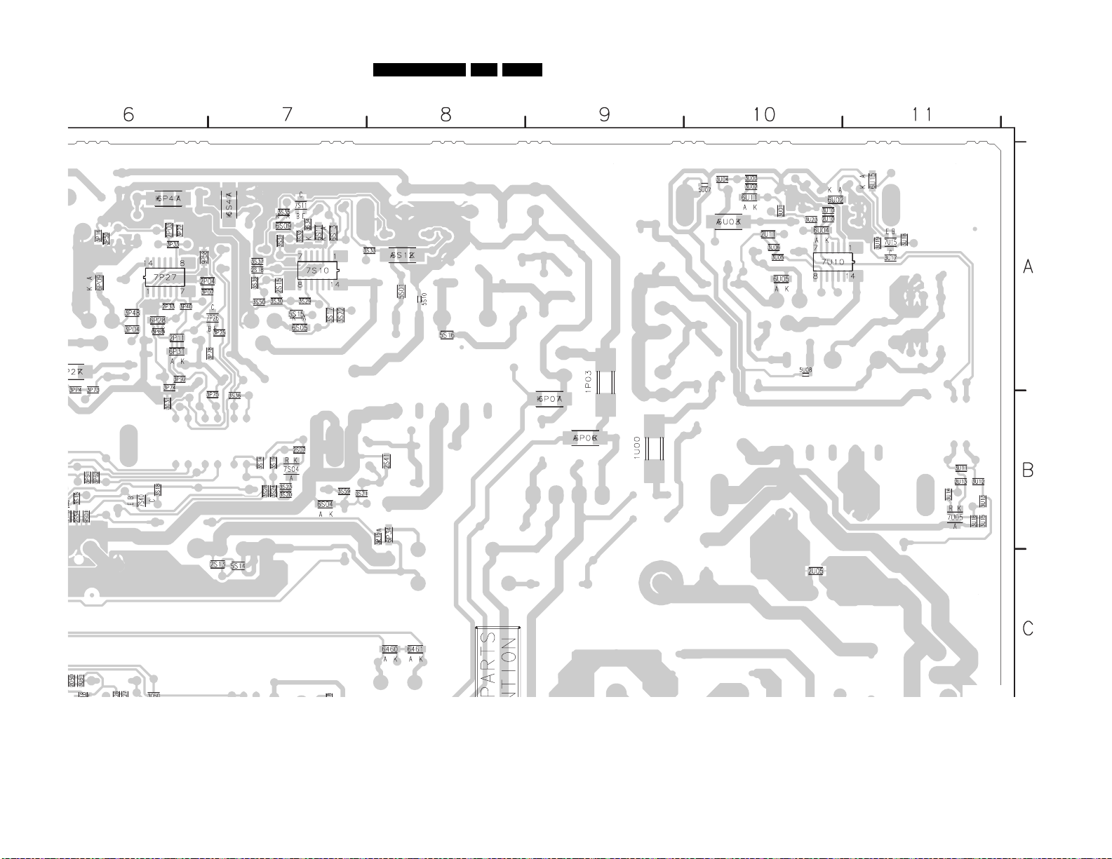
Circuit Diagrams and PWB Layouts
Part 2
G_15970_012b.eps
1
60306
Layout Display/Platform Supply 37” (Part 2 Bottom Side)
85BJ3.0E LA 7.

86BJ3.0E LA 7.
Circuit Diagrams and PWB Layouts
Layout Display/Platform Supply 37” (Part 3 Bottom Side)
Part 3
G_15970_012c.eps
160306

Circuit Diagrams and PWB Layouts
Part 4
G_15970_012d.eps
160306
Layout Display/Platform Supply 37” (Part 4 Bottom Side)
87BJ3.0E LA 7.
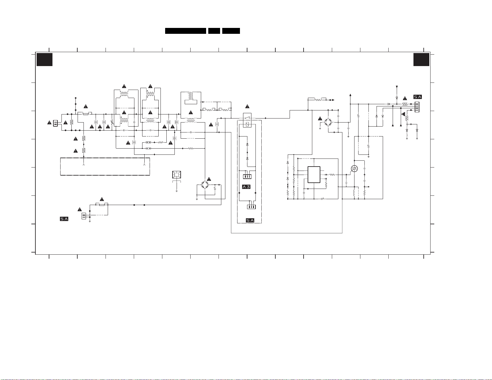
Circuit Diagrams and PWB Layouts
88BJ3.0E LA 7.
Display Supply 42”: Mains Filter & Stby A
1 2 3 4 5 6 7 8
MAINS FILTER + STANDBY PART A
A1 A1
9
A
3405
220R
MAINS FILTER
I411
470n
2401
470n
2410
I416
1n0
2407
1011
HEATSINK
HOT_GNDA
2 3
1 4
I455
5403
DTH40203H65
124
5402
DMF3547HB60
2406
47p
9003
3404
220R
GNDHOT
3
I412
9005
9011
3450
I442
6506
DF06M
3451
1R0
1R0
I444
I445
2408
470n
I415
I456
10u
2503
1450
G5PA-1-5VDC
6461
BAS316
I424
6460
BAS316
1B06
123
B3B-EH-A
TO
RELAY -
RELAY +
F425
COLD
GROUND
1305
123
TO
AUDIO-STANDBY
F424
B3B-EH-A
I413
6809
1N5062
1M0
3800
I814
I466
6808
1N5062
3806
470R
I816
I827
I815
20K
22K
3804
3807
I820
B
C
D
E
F
MAINS INPUT
95-264Vac
MAINS_L
B2P-VA-BF-BK
2
1
1308
MAINS_N
AUDIO-STANDBY
4
5405
F410
F411
F414
1400
F412
F413
PTF/65
T3.15AH 250V
(EUR+AP CHINA)
T4AH 250V(AP+US)
4M7
3401
F416
F415
F419
F418
TO
1
2
B2P-VA-BF-BK
3402
3403
1
GND screw
1306
I419
I473
4M7
4M7
1000
GNDHOT
470n
2400
F417
COLD GROUND
1401
PTF/65
T1AE 250V
F427
9009
F428
1
2
DMF2405H60
9001
I410
5400
2
DMF28
470n
2409
3400
1
V
2403
47p
1
4
3
3
4
5404
DMF28
2
3
9006
I474
5401
3
2
1 4
22n
2402
DMF3547HB60
I475
2404
47p
90079008
I463
1403
2405
220p
500V
1402
500V
I460
1001
1
GND screw
F430
F429
G
3104 313 6065.3
1 2 3 4 5 6 7 8 9 10
I813
I464
9810
7805
AVS1ACP08
7 6
2 3
9806
2802
I470
100p
10 11
3810
F426
12K
I810
GBJ6J
6807
HOT_GNDA
4
VDD
MODE
NC
I465
58
VM
VG
OSIN
I468
OSOUT
VSS
91K
3802
1
2806
47u 50V
12 13
400V_HOT_A
25V_HOT_A
I811
I812
56n
2803
2804
I817
3803
390R
56n
2817
HOT_GNDA
I467
2808
2815
10n
I471
7806
47n
I469
5804
6155
9814
330u
9813
9808
I462
2816
330u
9811
HOT_GNDA
100n
2810
AVS10CB
I825
100n
2809
I824
I826
4R7
9812
3805
100u
11 12 13
BYG10
400V_HOT_B
6157
BYG10
3406
6156
I461
BYG10
100R
F421
F422
6154
BYG10
HOT_P+
HOT_P-
3407
6158
HOT_GNDA
TO
AUDIO-STANDBY
1307
F420
1
2
3
4
F423
B4P-VH
100R
I472
6159
BYG10
BYG10
HOT_GNDB
G_15950_001.eps
040406
1000 D2
9812 E11
1001 D4
9813 C12
1011 E5
9814 C12
1305 F7
F410 B1
1306 F2
F411 B2
1307 B13
F412 B1
1308 C1
F413 B1
1400 C2
F414 B2
A
1401 F2
F415 C1
1402 D4
F416 C1
1403 D4
F417 C2
F418 C1
1450 C8
F419 C2
1B06 E7
F420 B13
2400 C2
F421 B13
2401 C5
F422 B13
2402 C3
F423 C13
2403 C3
F424 E8
2404 C4
F425 E7
2405 D3
F426 B10
2406 C6
B
F427 F2
2407 C5
F428 F2
2408 C6
F429 F4
2409 C2
F430 F4
2410 C5
I410 C3
2503 E6
I411 C5
2802 E9
I412 B6
2803 C11
I413 C8
2804 C11
2806 F10
I415 C7
2808 E11
I416 C5
2809 E12
I419 D2
C
I424 D7
2810 E12
2815 C11
I442 C6
I444 C6
2816 D12
I445 C7
2817 C11
3400 C3
I455 D5
I456 E7
3401 C1
I460 D4
3402 C2
I461 B13
3403 D2
I462 C12
3404 D6
I463 D4
3405 D4
I464 D9
3406 B13
I465 E10
3407 C13
D
I466 E9
3450 B6
3451 B7
I467 E11
3800 E9
I468 E10
I469 E11
3802 E10
I470 E10
3803 E11
I471 D11
3804 E9
I472 C13
3805 E12
I473 D2
3806 E9
I474 C4
3807 E9
I475 C4
3810 B10
I810 B10
5400 C3
I811 B11
5401 C4
E
I812 B11
5402 C6
5403 B6
I813 C10
I814 E9
5404 B4
I815 E9
5405 B3
I816 E9
5804 E11
I817 C11
6154 C12
I820 F9
6155 C12
I824 E12
6156 B13
I825 E12
6157 B13
I826 E12
6158 C13
I827 E9
6159 C13
F
6460 D7
6461 D7
6506 E6
6807 C10
6808 E9
6809 D9
7805 D10
7806 E11
9001 B3
9003 C6
9005 B6
9006 B4
G
9007 C4
9008 C3
9009 F2
9011 B7
9806 E9
9808 C12
9810 D10
9811 D11
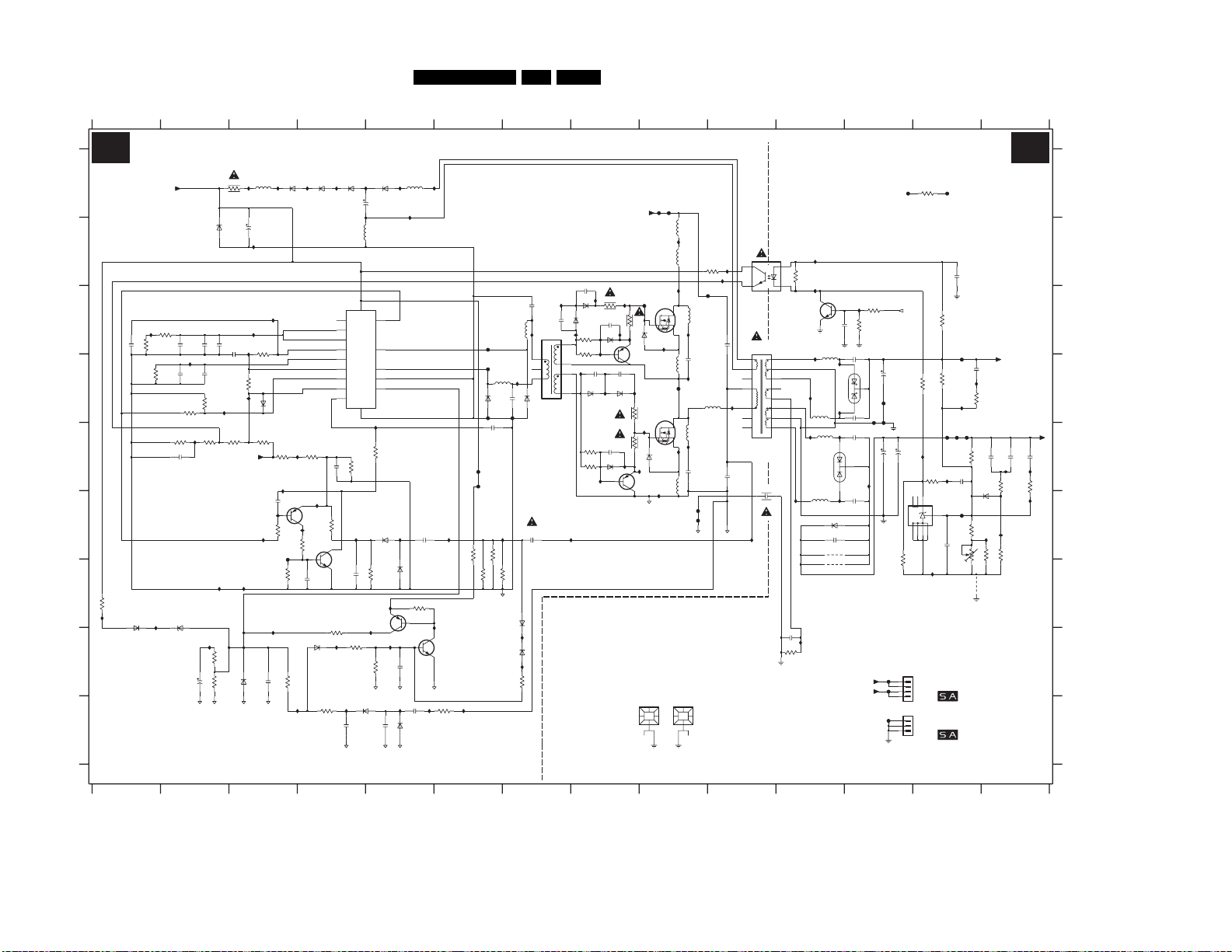
Circuit Diagrams and PWB Layouts
89BJ3.0E LA 7.
Display Supply 42”: Part A
1 2
SUPPLY PART A
A2 A2
A
25V_HOT_A
B
C
I103
560p
2040
3003
100K
3004
3002
10K
2004
27K
2005
VS-CONTROLLER
630V
100p
2021
200p
I009
630V
100p
2009
100p
D
2K7
3048
3043
1R0
3008
3009
I021
330R
3K3
E
2007
470n
16V
F
G
3067
100R
I143
H
BAS316
6009
I142
6020
PDZ18-B
I141
3010
3011
100u
2010
HOT_GNDA
HOT_GNDA
I
3 4 5
3000
I096
I097
6080
5017
50R
2002
I006
I007
I008
3006
I010
I029
6022
BZX384-C4V7
470u
3005
33K
10K
6001
3058
5M6
I025
HOT_GNDA
I022
2019
BYG22D
I027
BAS316
I105
3050
820K
SOFTSTART
CONTROL
I018
50V
15n
2027
10K
3066
F007
3027
100K
I135
10n
47R
3047
I134
I023
3064
6081
2034
I104
I028
4R7
BZX384-C22
100p
2006
1n025V
3007
10K
400V_HOT_A
470R
470R
HOT_GNDA
I078
6079
BYG22D
CONTROL
3053
680K
I020
BC857BW
7017
10K
50V
2n2
2026
BAS316
6051
3056
220R
(0V7)
4V9
(1V2)
4V9
(0V7)
I144
MC34067P
2V
4V9
(0V)
2050
3012
7018
BC847BW
3068
2K2
I136
9
1
2
3
16
6
8
7
11
HOT_GNDA
BIAS SUPPLY
6077
BYG22D
2003
5009
15
7001
VCC
EN|UA
OSCC
OSCR
OSCCC
OS
EAO
PGND
Ip
In
SOST
GND
4
68K
1n0
3061
CURRENT
PROTECTION
15K
I024
16V
470n
2008
3070
1K0
6006
I133
BAS316
47n
2046
I098
1m0
80R
VREF
OA
OB
FI
I012
3065
3013
BC857BW
I137
3071
HOT_GNDA
HOT_GNDA
6078
BYV27-200
17V
(7V6)
5
14
12
13
10
6K8
6011
BAS316
10K
I139
7009
10K
2048
5V1
(0V5)
7V3
(0V3)
7V3
(0V3)
0V01
(0V)
0V6
(5V)
I138
HOT_GNDA
1n0
I099
I033
6010
2077
I132
6017
HOT_GNDA
5010
1m0
I101
BAS316
3075
1K0
2n2
2047
10n
BAS316
6 7 8
I100
F003
F004
5016
80R
6005
BAS316
F008
16V100n
2016
F010
F006
3001
100R
3046
22R
3045
HOT_GNDA
I131
I034
22R
3021
GROUND GROUND
2015
10n
HOT_GNDA
I151
I036
50V
I140
7004
BC847BW
3055
220R
400V_HOT_A
2061
HIGH SIDE
2n2
3014
I038
I042
6007
I148
2063
470p
BAS316
100R
2072
2n2
6003
2060
BAS316
5001
80R
5015
I107
S13932-04
4
3
2
I108
2064
470p
6004 BAS316
F009
2014
2n2
2000V
22R
6016
BAS316
I083
6015
BZX384-C22
I082
10K
3089
COLD
HOT
1n0
I045
6
7
9
10
I081
I046
6027
3016
BAS316
2K2
3029
I109
2K2
I039
2062
2065
2n2
2n2
6008
6002
I052
BAS316
BAS316
2071
3020
2K2
1n0
6028
3019
I051
2K2
BAS316
I145
DRIVE
3015
I037
BC857BW
7007
3017
3018
F018
F002
STP15NK50ZFP
47R
6013
SML4744
I150
LOW SIDE
DRIVE
100R
STP15NK50ZFP
I057
47R
6012
I059
BC857BW
7008
I055
GND3
1009
HEATSINK
GNDA
7005
I294
7006
SML4744
9
F299
80R
5007
I146
80R
5008
I147
399V
80R
I111
2013
50R
5004
I110
F005
FLM 1/6W
5013
I112
2012
50R
5041
c002
F023
F300
HOT_GNDA
1010
HEATSINK
GNDA
3028
1K0
F029
5005
2000V
1n5
5040
80R
80R
I113
2000V
1n5
HOT_GNDA
10
HOT
GROUND GROUND
I080
3 2
I064
TCET1102(G)
1600V
10n
5002
BS51312-01
2017
8
7
6
5
3
I114
2
1
10n
2011
1600V
c001
I084
11
COLD
I062
7002
14
1K0
3033
I063
7030
BC847BW
GNDA
I116
5027
9
10
11
12
13
14
15
16
2000
470p
GNDA
80R
I117
5028
80R
5025
I073
80R
STTH2003CFP
6021
5026
I076
80R
BYW29FP-200
50V
2290
I124
50V
10n
3292
560R
3104 313 6065.3
1
2
3
4 5 6 7 8 9 10 11 12
12
I149
3031
10K
10n
47K
2039
3032
GNDAGNDA
2028
1n0
50V
I070
3
2m2
2020
2
6044
I072
I074
1
3
I077
6014
2035
1n0
9004
9010
F028
1
2044
STPS20L45CT
1n0
F017
50V
F027
GNDA
2029
17V3
50V
1n0
2022
1m8 35V
2
I075
2045
50V
1n0
GNDA
DC_PROT
A4
25V
2038
3030
13
F022
F021
3999
1K0
2023
470n
GNDA
3057
220R
F016
+12V
10n
2031
33K
3052
3022
35V
1m8
1
4
5
NC
236
18K
I119
680R
I085
3023
15K
7010
K
TL431ACD
R
A
7
I094
15K
3037
I120
F012
F025
F024
18K
3024
2033
MRS25 1%
I089
2024
220n
6023
16V
8
13V4
BAS316
F014
1%
1K8
3025
I093
16V
2030
100n
Vs
3034
470R
Voltage
Adj.
1%
3026
9002
GNDA
1304
+24Va
+12V
F030
F031
F032
GNDA
B4P-VH
B3P-VH
1309
1
AUDIO-STANDBY
2
3
4
1
AUDIO-STANDBY
2
3
TO
TO
13 14
14
1u0
50V
1u0
2025
I121
I088
8K2
3040
I092
RES
33K
3041
G_15950_002.eps
2032
3038
+24Va
4n7
33K
I122
040406
3070 H4
1009 I9
1010 I9
1304 H12
1309 I12
2000 F10
2002 B3
2003 A4
2004 C2
2005 D2
2006 C3
2007 E2
A
2008 G4
2009 D2
2010 H2
2011 E10
2012 E9
2013 D9
2014 F7
2015 F5
2016 E6
2017 C10
2019 H3
2020 D12
B
2021 C2
2022 E12
2023 B13
2024 E13
2025 E14
2026 G4
2027 F3
2028 D12
2029 E12
2030 F13
2031 D13
C
2032 E14
2033 E14
2034 C2
2035 F11
2038 E12
2039 C11
2040 C1
2044 D12
2045 F12
2046 I4
2047 I5
2048 I5
D
2050 E4
2060 C7
2061 C8
2062 D8
2063 C7
2064 D7
2065 D8
2071 E8
2072 C8
2077 H5
2290 H11
3000 A3
E
3001 F6
3002 C2
3003 C1
3004 D1
3005 C3
3006 D3
3007 E3
3008 E2
3009 E2
3010 H2
3011 H2
F
3012 F4
3013 G5
3014 C8
3015 C8
3016 C8
3017 D8
3018 E8
3019 E8
3020 E8
3021 G6
3022 D13
3023 E13
G
3024 E13
3025 F13
3026 G13
3027 G3
3028 B10
3029 C8
3030 G12
3031 C12
3032 C12
3033 B11
3034 F14
3037 D13
H
3038 E14
3040 E14
3041 F14
3043 D2
3045 G6
3046 F6
3047 H3
3048 D2
3050 E3
3052 D13
3053 E4
I
3055 I6
3056 I4
3057 C13
3058 E3
3061 E4
3064 F4
3065 E5
3066 F3
3067 G1
3068 H4
3071 H5
3075 G5
3089 H7
3292 H11
3999 A13
5001 C7
5002 C10
5004 D9
5005 C9
5007 B9
5008 B9
5009 B4
5010 A5
5013 E9
5015 C7
5016 D7
5017 A3
5025 E11
5026 F11
5027 D11
5028 D11
5040 D10
5041 E9
6001 D3
6002 D8
6003 C8
6004 D7
6005 D6
6006 I5
6007 C8
6008 D8
6009 G2
6010 G5
6011 F5
6012 E9
6013 C9
6014 F11
6015 H7
6016 G7
6017 I5
6020 H1
6021 E11
6022 H3
6023 F14
6027 C8
6028 E8
6044 D12
6051 H4
6077 A4
6078 A5
6079 A4
6080 A3
6081 B2
7001 C4
7002 B10
7004 H6
7005 C9
7006 D9
7007 D8
7008 E8
7009 G5
7010 F13
7017 F4
7018 F4
7030 C11
9002 G13
9004 F11
9010 G11
F002 C9
F003 C6
F004 D6
F005 D9
F006 E6
F007 F3
F008 D6
F009 D7
F010 E6
F012 E13
F014 F13
F016 D13
F017 D12
F018 B9
F021 A12
F022 A13
F023 F9
F024 E13
F025 E13
F027 E12
F028 D12
F029 C10
F030 H12
F031 H12
F032 I12
F299 A9
F300 F9
I006 B3
I007 C3
I008 C3
I009 D2
I010 D3
I012 D5
I018 E3
I020 F4
I021 E2
I022 F3
I023 F3
I024 F4
I025 F3
I027 C3
I028 G2
I029 G3
I033 F5
I034 F7
I036 F6
I037 C8
I038 C8
I039 D8
I042 C8
I045 C7
I046 C8
I051 E8
I052 D8
I055 E9
I057 E9
I059 E9
I062 B11
I063 B11
I064 B10
I070 D12
I072 D11
I073 E11
I074 E11
I075 E12
I076 F11
I077 F11
I078 A4
I080 B10
I081 F8
I082 H7
I083 H7
I084 F10
I085 E13
I088 E14
I089 E13
I092 F14
I093 F14
I094 G13
I096 A3
I097 A3
I098 A5
I099 A5
I100 A6
I101 A5
I103 C1
I104 D2
I105 E4
I107 C7
I108 D7
I109 D8
I110 D9
I111 C9
I112 E9
I113 E9
I114 D10
I116 C11
I117 D11
I119 D13
I120 D13
I121 E14
I122 F14
I124 H11
I131 I6
I132 I5
I133 I4
I134 I4
I135 H3
I136 H4
I137 H5
I138 H5
I139 G5
I140 G6
I141 H2
I142 G1
I143 G1
I144 A4
I145 E8
I146 B9
I147 C9
I148 C7
I149 C12
I150 D9
I151 I5
I294 C9
c001 F10
c002 F9

Circuit Diagrams and PWB Layouts
V
MODE
VM
OSIN
VSS
OSOUT
VG
NC
VDD
6D61 D8
ID67 E11
FD25 E8
IH11 C11
ID69 E12
MAINS INPUT
(EUR+AP CHINA)
FD19 C2
ID66 E10
ID70 E10
ID64 D10
FD24 E8
IH10 C11
ID65 E11
12
9 11
8
12
6 7
10
9
T5AH 250V(AP+US)
TO
2D03 C4
2D04 C5
IH17 C11
ID61 D12
2H10 E12
2H15 C12
2H16 D12
2H17 C11
3D00 C3
3D04 D6
3D05 D5
3D50 C7
3H10 B10
A
3H07 F9
5D05 B4
5DO4 B5
5H04 F12
6A54 C13
6A55 C12
6D60 D8
3H00 E9
6H07 C11
2H06 F10
2H09 E12
2H04 C11
COLD GROUND
7H05 E10
7H06 E11
6H09 D9
6H08 E9
9H06 E10
9H08 D12
2H08 E11
E
F
G
D
E
F
2H03 C11
6
2D10 C6
2D07 D6
G
2D08 C7
2D09 C3
ID68 E11
IH13 C10
IH12 C11
95-264Vac
10 11
RELAY +
2
1U01 E4
13
2D00 C2
2D01 C5
1U11 E5
1
ID62 D12
ID63 D5
IH14 E9
IH15 E9
IH16 E9
9U03 D6
9U05 B7
9U06 C5
9U07 D5
9U08 D4
9U10 B7
FD10 B2
FD11 B2
FD12 C1
FD13 C2
ID16 C6
ID46 C4
ID48 D5
B
3D51 C7
3H05 F12
3H04 F9
C
3H02 E11
ID47 C4
3H03 E11
13
1D03 D5
1C05 E8
1D50 C8
1D02 D5
1D00 C2
T3.15AH 250V
A
B
C
D
ID24 D8
ID44 C7
ID45 C7
FD26 B11
ID10 C3
ID11 C6
ID12 C7
ID13 C8
ID15 C7
FD16 C2
5D03 B6
5D00 C4
5D02 C6
4
2H02 F10
MAINS FILTER
5
2D06 C6
3
2D05 D4
3
IH25 E12
IH26 E12
1
MAINS FILTER + STANDBY PART B
RELAY -
IH24 E12
52 4
IH20 F9
5D01 C5
FD17 C2
FD14 C2
FD18 C2
FD15 C1
9H13 D12
9H14 C12
9U01 C4
ID55 D6
9H10 D10
COLD GROUND
9H12 F12
9H11 D12
ID42 C6
25V_HOT_B
7 8
3H10
12K
6A55
BYG10
123
ID55
58
1
1C05
B3B-EH-A
AVS1ACP08
7H05
7 6
2 3
4
1 4
2 3
DMF3547HB60
5D01
4
1
3
2
IH11
DMF28
5D00
3D00
PTF/65
1D00
ID15
MAINS_N
ID12
2 3
220p
2D05
DMF3547HB60
5D02
1 4
2
3
G5PA-1-5VDC
1D50
DMF2405H60
5D05
1
4
IH20
9H13 9H08
HOT_GNDB
HOT_GNDB
HOT_P+
HOT_P-
2H02
100p
ID44
ID16
56n
2H04
1U11
HEATSINK
2H16
330u
220R
3D04
FD16
ID69
IH15
IH12
FD11
FD13
FD14
FD12
ID11
470n
2D01
1
2
4
3
400V_HOT_B
DTH40203H65
5D03
2D07
1n0
GND screw
1U01
1
HOT_GNDB
56n
2H03
ID47
3H07
22K
9H12
ID46
4R7
3H05
9U07
7H06
AVS10CB
2D08
470n
IH16
IH14
9U05
470n
2D00
IH13
IH26
IH17
470n
2D09
470n
2D10
BAS316
6D60
ID68
100u
5H04
3H00
1M0
3H03
390R
330u
2H15
ID61
FD10
FD15
FD26
IH25
ID65
BYG10
6A54
ID70
FD24
FD18
FD25
6D61
BAS316
ID67
100n
2H10
1
3
2
IH10
DMF28
5DO4
4
2H06
47u 50V
1D02
500V
FD19
FD17
9U08
9U01
ID13
ID24
ID62
ID48
9U06
IH24
ID64
3D50
1R0
ID66
9H10
2H09
100n
3H02
91K
3H04
18K
HOT_GNDB
9H06
ID45
9U03
ID42
ID10
9U10
3D51
1R0
2H08
47n
MAINS_L
1N5062
6H08
1N5062
6H09
GBJ6J
6H07
10n
2H17
9H14
9H11
G_15950_003.eps
040406
3104 313 6065.3
A3 A3
Display Supply 42”: Mains Filter & Stby B
90BJ3.0E LA 7.

Circuit Diagrams and PWB Layouts
IA44 C14
IU84 F10
IU85 E13
IU86 D13
IU88 E14
IU89 E13
IU92 F14
IU93 F14
IU94 G13
IU96 A3
IU97 A3
IU98 A5
IU99 A5
cU01 F10
cU02 F9
BIAS SUPPLY
LOW SIDE
4V9
0V6
(0V)
(0V5)
GROUNDGROUND
GROUND
0V01
(7V6)
(0V7)
250V
IU27 C3
IA03 C1
IU28 G2
IU29 G3
IU33 F5
IU34 F6
IU36 F6
IU37 C8
IU38 C8
IU39 D8
IU41 H2
IU42 C8
IU45 C8
IU46 C8
IU51 E8
IU52 D8
IU55 F9
IU57 E9
IU59 E9
IU62 B11
IU63 C11
IU64 C9
IU73 E11
IU74 E11
IU76 F11
IU77 F11
IU79 B9
IU80 G11
4V9
VS-CONTROLLER
IU81 F8
IU82 H7
IU83 H7
FB94 H13
IA45 E8
IA46 B9
IA47 C9
IA48 C7
IA49 C12
IA50 D9
IA51 I5
IB90 G12
IB91 G12
IB92 H11
IB93 H12
IB94 C9
IU05 A4
IU06 B2
IU07 C3
IU08 C3
IU09 D2
IU10 D3
IU12 E5
IU18 E3
IU20 F4
IU21 E2
IU22 F3
IU23 F3
IU24 F4
IU25 F3
CURRENT
VSND_NEG
CONTROL
6U20 H1
IA04 D2
IA05 E3
IA07 C7
IA08 D7
IA09 D8
IA10 D9
IA11 C9
IA12 E9
IA13 E9
IA14 E10
IA20 E13
IA21 E14
IA22 F14
IA23 F11
IA24 G11
IA31 I6
IA32 I5
IA33 I4
IA34 I3
IA35 H3
IA36 H4
IA37 H5
IA38 H5
IA39 G5
IA40 H6
IA42 H1
COLD
5V1
17V
DRIVE
IA43 G1
5U09 B5
FB95 H13
FB96 G14
FB97 G13
FB98 H13
FC00 F9
FU02 C9
FU03 C6
FU04 D6
FU05 D9
FU06 E6
FU07 F3
FU08 D6
FU09 D7
FU10 E6
FU12 E13
FU14 F13
FU17 D12
FU18 B9
FU23 F9
FU24 E13
FU25 E13
FU27 E12
FU28 D12
FU29 C10
FU30 I12
FU32 I12
Adj.
SOFTSTART
FU99 A9
IA00 A5
IA01 A5
3U45 G6
6U21 E11
6U22 H3
6U23 F14
6U27 C8
6U28 E8
6U51 H4
6U77 A4
6U78 A5
6U79 A4
6U81 B2
7U01 C4
7U02 B10
7U04 H5
7U05 C9
7U06 D9
7U07 D8
7U08 E8
7U09 G5
7U10 F13
7U17 F4
7U18 G4
7U30 C11
9U02 G13
9U04 B5
FB90 H13
FB92 G13
17V3
PROTECTION
GROUND
FB93 G13
3U13 G5
5U10 A5
5U13 E9
5U15 C7
5U16 D6
5U17 A3
5U25 E11
5U26 F11
5U40 D10
5U41 E9
6B91 G11
6B93 H11
6U01 D3
6U02 D8
6U03 C8
6U04 D7
6U05 D6
6U06 I4
6U07 C8
6U08 D8
6U09 H2
6U10 G5
6U11 F5
6U12 E9
6U13 C9
6U15 H7
6U16 G7
GND_SND
(5V)
399V
CONTROL
6U17 I5
2U40 C1
3U46 F6
3U47 H3
3U48 D2
3U50 E3
3U52 D13
3U53 E4
3U55 I6
3U56 I4
3U57 C13
3U58 E3
3U61 E4
3U64 F4
3U65 E5
3U66 F3
3U67 G1
3U68 H4
3U70 H4
3U71 H5
3U75 G5
3U89 H7
5B91 G13
5B92 H13
5B93 G13
5U01 C7
5U02 D10
5U04 D9
2V
(0V7)
5U05 C9
5U07 B9
5U08 B9
2U05 D2
3U14 C8
3U15 C8
3U16 C8
3U17 D8
3U18 E8
3U19 E8
3U20 E8
3U21 G6
3U22 D13
3U23 E13
3U24 E13
3U25 F13
3U26 G13
3U27 G3
3U28 B9
3U29 C8
3U30 G12
3U31 C12
3U32 C12
3U33 B11
3U34 F14
3U38 E14
3U39 D13
3U40 E14
3U41 F14
3U43 D2
VSND_POS
13V4
Voltage
FLM 1/6W
1%
9
2U45 F12
2U46 I4
2U47 I5
2U48 I5
2
U50 E4
2U60 C7
2U61 C8
2U62 D8
2U63 C7
2U64 D7
2U65 D8
2U71 E8
2U72 C8
2U77 H5
3B92 G11
3U00 A3
3U01 F6
3U02 C2
3U03 C1
3U04 D1
3U05 C3
3U06 D3
3U07 E3
3U08 E2
3U09 E2
3U10 H2
(0V3)
Vs
MRS25 1%
3U11 H2
3U12 F4
H
2U06 C3
2U07 E2
2U08 G4
2U09 D2
2U10 H2
2U11 E10
2U12 E9
2U13 D9
2U14 F7
2U15 F5
2U16 E6
2U17 D10
2U19 H3
2U21 C2
2U22 E12
2U23 B14
2U24 E13
2U25 E14
2U26 G4
2U27 F3
2U29 E12
2U30 F13
2U32 E14
2U33 E14
2U34 C2
2U38 E12
1%
4V9
HOT
(1V2)
2U39 C12
10 11 12 13 14
1
2 3 4 5 6 7 8 9 10 11 12 13 14
(0V)
(0V3)
7V3
2B93
H11
2B94 H12
2U00 F10
2U02 B3
2U03 A4
2U04 C2
I
A
B
C
D
E
F
G
H
I
1303 I12
1320 I12
1M02 H14
1U07 G11
1U09 I9
1U10 I10
2B90 G11
2B91 G11
2B92 G12
HOT
HIGH SIDE
DRIVE
1 2 3 4 5 6 7 8
COLD
A4
7V3
SUPPLY PART B
A4
A
B
C
D
E
F
G
10K
3U02
2U04
200p
630V
2U23
470n
33u
5B91
3U40
8K2
IU73
3U13
10K
IA39
6U16
BAS316
80R
5U07
IU27
2U72
1n0
FB97
BAS316
6U02
1
2
3
4
2U60
2n2
IU34
1303
B4P-VH
2K2
FU27
22R
+24Vb
3U20
IA04
3U45
5U04
50R
820K
3U50
FB90
3U25
10n
1600V
2U11
1K8
5AT
1U07
220R
3U52
7U05
STP15NK50ZFP
1n5
IU24
2U13
2000V
GNDB
IU98
2K2
2U17
3U19
HOT_GNDB
GNDB
10n 1600V
FB98
10n
50V
2B90
100n
2U00
470p
2U30
16V
3U66
10K
IU07
HOT_GNDB
6U13
FB95
IU09
SML4744
1
2
3
B3P-VH
1320
BYW29EX-200
6B91
FU09
3K3
3U09
80R
5U09
2m2
2B94
6U22
BZX384-C4V7
7U07
IU76
BC857BW
6U03
BAS316
100R
3U17
1n0
3U67
100R
2U24
2U48
FB94
16V
220n
4R7
3U00
IU92
IA13
IU74
BZX384-C22
6U15
330R
3U39
GND_SND
3U57
220R
47n
6U06
BAS316
FU23
2U46
2B91
470p50V
BAS316
6U17
FU03
2U21
100p
5U16
IA32
80R
400V_HOT_B
IA09
9U04
FU32
IB93
FU24
IU77
5U25
80R
5B93
6U11
BAS316
IA35
33u
FU06
IA07
HOT_GNDB
FU99
IA31
2K2
3U68
GNDB
7U08
BC857BW
7U18
BC847BW
IU39
IU46
3U06
10K
IA47
IU93
IA50
HOT_GNDB
cU01
IU83
IU86
IU82
IU23
2B92
2m2
2U03
1m0
5U26
FU12
80R
470R
3U11
IA34
6U78
BYV27-200
IA22
5U40
80R
HEATSINK
3U71
10K
2000V
2n2
1U10
2U02
2U14
IA11
470u
2n2
IB94
2U65
3U38
33K
33u
5B92
OSCR
2
PGND
13
SOST
11
VCC
15
5
VREF
4
GND
7
In
Ip
8
OA
14
12
OB
OS
16
OSCC
1
3
OSCCC
MC34067P
7U01
6
EAO
9
EN|UA
10
FI
IA37
1K0
3U28
IU20
IA03
IU05
2U50
400V_HOT_B
GNDB
1n0
50R
IU79
IA21
5U17
IU33
2U29
50V
IU59
1n0
50V
2n2
2U26
2B93
3U43
1R0
+24Vb
50V470p
22R
15K
3U12
3U21
6U77
BYG22D
33K
IU10
3U05
6U10
BAS316
3U56
220R
IU88
3
2
1U09
HEATSINK
6U21
STTH2003CFP
1
6U01
BAS316
IU12
IU63
IU25
IU21
IA08
IA45
FU04
IU28
HOT_GNDB
2U63
470p
80R
5U13
50R
5U41
IU52
GNDB
IU45
2U64
470p
GNDB
IA36
10K
3U64
470n16V
2U08
IU51
IU08
IU99
3U55
220R
HOT_GNDB
HOT_GNDB
IU64
BAS316
6U07
3U14
100R
3U15
47R
1m0
5U10
10K
3U07
A
236
7
K
1
4
5
R
8
7U10
TL431ACD
2K7
3U48
6U23
BAS316
IA01
3U18
47R
7U06
STP15NK50ZFP
3U41
33K
6U79
BYG22D
BAS3166U05
680K
3U53
470R
IA42
FU08
3U26
FB93
IU38
10K
3U89
FB96
10n
2U19
IA23
FU25
1K0
3U33
2U38
1m8 35V
IA10
2K2
3U29
BC847BW
7U30
SML4744
6U12
2U27
50V
15n
68K
3U61
80R
5U05
2U40
18K
3U30
560p
IB92
IB91
6U51
BAS316
2U77
2n2
25V_HOT_B
9U02
FU02
IA51
IA38
FU14
FU29
BAS316
6U28
3U75
1K0
1
2
3
4
5
6
7
2
3
5
6
7
8 9
B7B-EH-A
1M02
1
10
11
12
13
14
15
16
5U02
BS51312-01
IA00
IA40
2U10
100u
630V
2U05
100p
10n
IA48
1K0
3U70
2U39
cU02
IU62
GNDB
FU10
HOT_GNDB
FU28
FC00
22R
7U09
BC857BW
560R
3B92
3U46
2U45
1n0 50V
IA46
FB92
3U04
2U06
27K
25V1n0
BZX384-C22
6U81
IU94
IU41
IB90
IA05
IU22
IA14
2U15
50V
10n
2n2
2U12
1n5
2U61
2000V
5U15
IA43
2U25
50V1u0
80R
6U09
IU42
PDZ18-B
5M6
3U58
6U04 BAS316
100p
2U09
BC847BW
7U04
IA49
IA44
3U16
2K2
IU85
6U27
BAS316
7U02
TCET1102(G)
14
3
2
2U34
2U22
1m8 35V
100p
FU18
2n2
HOT_GNDB
HOT_GNDB
2U62
470n
16V
GNDB
HOT_GNDB
3U01
100R
2U07
3U65
GNDB
6K8
IU80
3U23
15K
3U27
100K
IA33
IU89
IU36
IA24
10K
3U31
2U16
IA12
16V100n
2U47
IA20
FU07
10n
3U34
3U03
100K
IU18
IU06
3U32
47K
BAS316
6U08
IU37
10
2
3
4
6
7
9
IU55
5U01
S13932-04
FU05
GNDB
GNDB
FU30
3U08
330R
1n0
2U71
IU57
IU29
FU17
IU84
BYW29EX-200
6B93
3U10
470R
3U47
47R
6U20
BAS316
HOT_GNDB
IU97
3U24
18K
7U17
BC857BW
80R
5U08
IU96
IU81
HOT_GNDB
3U22
330R
4n7
2U33
1u0
2U32
DC_PROT
DC_PROT
TO
AUDIO-STANDBY
TO
AUDIO-STANDBY
TO
AUDIO-STANDBY
G_15950_004.eps
040406
3104 313 6065.3
A4 A4
91BJ3.0E LA 7.
Display Supply 42”: Part B
NC

Circuit Diagrams and PWB Layouts
G_15950_005.eps
040406
3104 313 6065.3
1000 B1
1001 A2
1009 B10
1010 C10
1011 C4
1303 E11
1304 B11
1305 A4
1306 A5
1307 D5
1308 C1
1309 B11
1320 E11
1400 B1
1401 A5
1402 A3
1403 A3
1450 B4
1B06 A4
1C05 D4
1D00 D1
1D02 F2
1D50 E4
1M02 F11
1U01 D3
1U07 F10
1U09 E10
1U10 G10
1U11 G4
2000 A9
2002 B8
2003 B7
2004 A8
2005 A8
2010 A8
2011 C7
2012 D9
2013 C7
2014 A9
2017 B7
2020 C11
2022 B11
2025 A10
2033 A11
2038 B10
2400 B1
2401 B4
2402 A2
2403 A3
2404 A3
2405 A3
2406 B3
2407 B4
2408 C3
2409 B1
2410 B4
2503 A5
2803 C4
2804 C5
2806 B5
2808 C5
2809 D4
2810 D5
2815 B4
2816 B6
2817 A6
2B92 F10
2B94 F10
2D00 E2
2D01 E4
2D05 D4
2D07 E4
2D08 E4
2D09 E2
2D10 E4
2H03 F5
2H04 F5
2H06 F5
2H08 F5
2H09 G5
2H10 G6
2H15 E5
2H16 E6
2H17 E6
2U00 E9
2U02 E8
2U03 E7
2U04 D7
2U05 D7
2U10 D8
2U11 F8
2U12 G9
2U13 G8
2U14 D8
2U17 F7
2U22 F11
2U25 D11
2U33 D11
2U38 E10
3000 A6
3014 C7
3015 C7
3017 D8
3018 D7
3026 A10
3050 A7
3053 A7
3058 A7
3400 B2
3401 C1
3402 C1
3403 C1
3404 B3
3405 B3
3406 D5
3407 D6
3450 C2
3451 C3
3800 B5
3803 C5
3805 C5
3807 B5
3810 B5
3D00 D1
3D04 F2
3D50 G2
3D51 G4
3H00 E5
3H03 F6
3H05 G4
3H07 E5
3H10 E5
3U00 D5
3U14 F7
3U15 G7
3U17 G8
3U18 G8
3U26 D10
3U50 E7
3U53 D6
3U58 E7
5001 C7
5002 B9
5004 C7
5005 D7
5007 A6
5008 A6
5009 B8
5010 B7
5013 D8
5015 B7
5016 B7
5017 A5
5025 B10
5026 B10
5027 C9
5028 C10
5040 C7
5041 D9
5400 A1
5401 A2
5402 C3
5403 D2
5404 B3
5405 A2
5804 C5
5B91 F11
5B92 F11
5B93 F11
5D00 D1
5D01 D3
5D02 F3
5D03 F2
5D05 E2
5DO4 E3
5H04 F5
5U01 F7
5U02 F9
5U04 F7
5U05 G8
5U07 E6
5U08 E6
5U09 E8
5U10 E8
5U13 G9
5U15 E7
5U16 E7
5U17 D6
5U25 E10
5U26 E10
5U40 F7
5U41 G9
6014 A11
6021 B10
6044 D10
6078 B7
6506 B4
6807 C4
6808 B5
6809 B5
6B91 G10
6B93 G11
6H07 G5
6H08 E5
6H09 E5
6U21 E10
6U78 E7
7001 A7
7002 A9
7005 D7
7006 C8
7805 B5
7806 D5
7H05 F6
7H06 G6
7U01 E7
7U02 D9
7U05 G7
7U06 G9
9001 A1
9003 B4
9004 B11
9005 D2
9006 B2
9007 B3
9008 A1
9009 A5
9010 B11
9011 C3
9080 A8
9082 C4
9088 A10
9089 D2
9090 A10
9091 A9
9092 B8
9093 A8
9094 B7
9095 B9
9096 C7
9097 D6
9098 C4
9099 B3
9808 C6
9811 C6
9812 C5
9813 C6
9814 B6
9H08 F6
9H11 F6
9H12 F5
9H13 E6
9H14 E6
9H15 F6
9H16 G5
9H17 C1
9U01 E1
9U03 E4
9U04 E8
9U05 G3
9U06 E3
9U07 E3
9U08 E2
9U09 G8
9U10 F4
9U50 E3
9U51 E9
9U52 E5
9U53 F5
9U54 G7
9U55 D8
9U56 F10
9U58 E7
9U59 E5
9U60 D4
9U61 D5
9U62 D5
9U63 B11
9U65 B11
9U66 D10
9U67 A7
9U68 B7
9U69 A8
9U70 A8
9U71 B7
9U72 B7
9U73 B7
9U74 D7
9U76 E8
9U77 E9
9U78 E9
9U79 E8
9U80 E7
9U81 E7
9U82 F7
9U83 E7
9U84 G4
9U85 E6
9U86 B9
9U87 B9
9U88 F3
9U90 E2
9U91 E2
Layout Display Supply 42” (Top Side)
92BJ3.0E LA 7.

Circuit Diagrams and PWB Layouts
Part 1
G_15950_006a.eps
Part 2
G_15950_006b.eps
Part 4
G_15950_006d.eps
Part 3
G_15950_006c.eps
G_15950_006.eps
040406
3104 313 6065.3
2006 A5
2007 A5
2008 A5
2009 A4
2015 A4
2016 A5
2019 A4
2021 A4
2023 A2
2024 A2
2026 A5
2027 A5
2028 D2
2029 B2
2030 A1
2031 A2
2032 A2
2034 A4
2035 B1
2039 A1
2040 A5
2044 D2
2045 B2
2046 A4
2047 A4
2048 A4
2050 A5
2060 C5
2061 C5
2062 C5
2063 C5
2064 C5
2065 C4
2071 C4
2072 C6
2077 A4
2290 B3
2802 C7
2B90 F3
2B91 G1
2B93 G1
2H02 F7
2U06 E5
2U07 E5
2U08 D5
2U09 D4
2U15 D4
2U16 E5
2U19 D4
2U21 D4
2U23 D2
2U24 D1
2U26 D5
2U27 D5
2U29 E2
2U30 D1
2U32 D1
2U34 D4
2U39 D1
2U40 E5
2U45 E2
2U46 D4
2U47 D4
2U48 E4
2U50 D5
2U60 G5
2U61 F5
2U62 G4
2U63 F5
2U64 F5
2U65 G4
2U71 G4
2U72 G5
2U77 D4
3001 A4
3002 A5
3003 A4
3004 A4
3005 A5
3006 A5
3007 A5
3008 A5
3009 A5
3010 A4
3011 A4
3012 A5
3013 A5
3016 C6
3019 C4
3020 C4
3021 A4
3022 A1
3023 A2
3024 A2
3025 A1
3027 A5
3028 A4
3029 C6
3030 A2
3031 A1
3032 A1
3033 A3
3034 A1
3037 A2
3038 A1
3040 A1
3041 A1
3043 A5
3045 A4
3046 A4
3047 A4
3048 A5
3052 A2
3055 A4
3056 A4
3057 A2
3061 A5
3064 A5
3065 A5
3066 A5
3067 A4
3068 A4
3070 A4
3071 A4
3075 A4
3089 A4
3292 B3
3802 C7
3804 C7
3806 C7
3999 C2
3B92 F3
3H02 F7
3H04 F7
3U01 D4
3U02 D5
3U03 D4
3U04 E4
3U05 D5
3U06 D5
3U07 E5
3U08 E5
3U09 E5
3U10 E4
3U11 D4
3U12 D5
3U13 D5
3U16 G5
3U19 G4
3U20 G4
3U21 D4
3U22 E1
3U23 D1
3U24 D1
3U25 D1
3U27 D5
3U28 D3
3U29 G5
3U30 D1
3U31 E1
3U32 D1
3U33 D3
3U34 D1
3U38 D1
3U39 E1
3U40 D1
3U41 D1
3U43 D5
3U45 D5
3U46 D5
3U47 D4
3U48 D5
3U52 D2
3U55 D4
3U56 D4
3U57 D2
3U61 D5
3U64 D5
3U65 D5
3U66 D5
3U67 E4
3U68 D4
3U70 D4
3U71 D4
3U75 D4
3U89 D3
6001 A5
6002 C4
6003 C5
6004 B5
6005 A5
6006 A4
6007 C5
6008 C5
6009 A4
6010 A5
6011 A5
6012 C4
6013 C5
6015 A4
6016 A4
6017 A4
6020 A4
6022 A4
6023 A1
6027 C6
6028 C4
6051 A4
6077 B5
6079 A6
6080 A6
6081 B4
6154 D6
6155 D6
6156 D7
6157 E7
6158 C6
6159 D6
6460 A8
6461 A8
6A54 D7
6A55 D7
6D60 D8
6D61 D8
6U01 D5
6U02 G3
6U03 G5
6U04 E5
6U05 E5
6U06 D4
6U07 F5
6U08 G4
6U09 D4
6U10 D4
6U11 D5
6U12 F3
6U13 F5
6U15 D4
6U16 D3
6U17 E4
6U20 E4
6U22 D4
6U23 D1
6U27 G5
6U28 G4
6U51 D4
6U77 E4
6U79 D6
6U81 E4
7004 A4
7007 C6
7008 C5
7009 A4
7010 A2
7017 A5
7018 A5
7030 A1
7U04 D4
7U07 G5
7U08 G4
7U09 D4
7U10 D2
7U17 D5
7U18 D5
7U30 E1
9002 A2
9085 A1
9806 C7
9810 C7
9H06 F7
9H10 F7
9U02 D2
9U57 D1
Layout Display Supply 42” (Overview Bottom Side)
93BJ3.0E LA 7.

Circuit Diagrams and PWB Layouts
G_15950_006a.eps
040406
Part 1
Layout Display Supply 42” (Part 1 Bottom Side)
94BJ3.0E LA 7.
Circuit Diagrams and PWB Layouts
G_15950_006b.eps
040406
Part 2
Layout Display Supply 42” (Part 2 Bottom Side)
95BJ3.0E LA 7.
Circuit Diagrams and PWB Layouts
G_15950_006c.eps
040406
Part 3
Layout Display Supply 42” (Part 3 Bottom Side)
96BJ3.0E LA 7.
Circuit Diagrams and PWB Layouts
G_15950_006d.eps
040406
Part 4
Layout Display Supply 42” (Part 4 Bottom Side)
97BJ3.0E LA 7.

Circuit Diagrams and PWB Layouts
COLD GROUND
FS13 C2
FS15 C1
FS18 C2
FS20 D7
FS21 C7
IS03 C7
IS06 C3
IS08 C5
IS13 C8
IS14 C4
IS17 D6
IS18 D2
IS19 D4
HOT GROUND
3S11 D2
3S12 D2
5S00 D8
5S01 C3
5S02 C8
5S03 C5
6S07 C7
9S00 D8
9S01 C8
FS11 D8
FS12 C1
2S00 C2
2S01 B2
2S02 B3
2S03 C7
2S04 C7
2S07 D4
2S15 D8
3S05 D5
3S08 C1
3S09 C3
COLD GROUND
MAINS INPUT
8
A
B
C
D
E
7 8
1 2 3 4 5 6 7
1S02 D3
1S03 D3
1S04 B2
198-264Vac
MAINS FILTER + STANDBY
1 2 3 4 5 6
T3.15AH 250V(EUR)
MAINS FILTER
A
B
C
D
E
1308 C1
1410 C8
1S00 C2
100p
2S02
100p
2S01
FS13
FS12
56n
2S03
1S02
500V
FS20
FS21
2 3
4M7
3S11
DMF28
5S01
1 4
FS18
4M7
3S12
GBJ6J
6S07
2S15
220u 400V
12
43
5S03
IS08
2S07
1n0
4M7
3S08
IS14
2S04
56n
GNDHOT
470n
2S00
1
400V_HOT
FS15
1
1S04
GND screw
IS18
1S03
GND screw
IS17
IS03
IS13
5S00
80R
FS11
80R
5S02
9S00
GNDHOT2
9S01
220R
3S05
3S09
1S00
T 1.0A
1410
IS06
2
IS19
1308
1
G_15950_007.eps
040406
3104 313 6146.3
AC1 AC1
Display Supply 26”: Mains Filter & Stby
98BJ3.0E LA 7.
V

Circuit Diagrams and PWB Layouts
D
E
F
G
A
B
C
D
E
F
G
1S22 C8
1U01 F5
1U11 G8
2U01 D10
2U02 B2
2U03 B7
2U04 B8
2U05 B8
2U06 C6
2U07 B8
2U08 F8
2U09 F1
3U05 C4
2U10 F2
2U11 C4
2U12 D8
1 2 3 4
HOT-GROUND
8
8 9 10 11 12
1 2 3 4 5 6 7
3U21 E7
9 10 11 12
A
B
C
AC5
2U13 D8
2U14 C10
2U15 E4
1316 D11
1317 D12
1319 C12
2U20 G7
2U22 A5
2U25 B8
2U26 C8
2U27 C8
2U28 C8
2U29 C7
3999 G10
3U01 D2
3U02 D3
3U03 E3
3U04 D3 3U36 F8
3U06 C4
3U07 C4
3U08 C5
3U09 C5
3U10 F2
3U11 D7
3U12 D8
5 6 7
3U13 D9
3U14 D8
3U15 E9
3U16 E9
3U17 D5
3U18 E3
3U19 E3
3U20 E5
3U50 F12
3U22 A6
3U23 D2
3U24 B4
3U25 E6
3U26 F5
3U27 E5
3U28 G4
AC3 (2X)
2U16 B10
2U17 B2
2U18 B3
3U29 F7
3U30 A6
3U31 E10
3U32 E4
3U33 E4
3U34 E10
3U35 F9
6U02 E2
3U37 E8
3U38 B4
3U39 B5
3U40 C4
3U41 C4
3U42 C3
3U43 G7
COLD-GROUND
SUPPLY
COLD-GROUND
3U44 F12
3U45 E8
3U46 C7
3U47 B11
3U48 B11
3U49 B11
6U41 E9
3U51 F12
3U91 C9
3U92 C9
3U93 C9
5U00 B6
5U03 B5
5U05 B2
5U06 D5
5U07 G5
5U08 C6
5U11 B9
5U12 C9
5U13 C8
5U17 B10
6U01 E6 9U21 E11
6U03 E4
6U04 E2
6U05 C4
6U06 B4
6U07 B9
6U08 E9
6U11 D3
AC3
6U15 F3
6U22 B5
6U23 B6
6U25 E4
6U26 F4
6U35 C8
6U36 C8
6U40 F11
FU10 C87U01 D7
7U02 C4
7U03 E5
7U04 E7
7U05 E7
7U07 F7
7U08 F8
7U10 C2
7U15 E2
7U16 F4
9U06 D5
9U17 B10
9U18 B10
9U20 E11
IU22 C4
9U22 F11
9U23 F11
9U24 F11
9U25 F10
9U26 F11
9U99 E11
FT01 G10
AC3
AC3
RES
FT02 G10
FU01 E7
FU02 C5
FU03 B8
FU04 C8
FU05 B11
FU06 C11
FU07 C5
FU08 C10
FU09 C11
IU52 B3
FU11 D6
FU12 D7
FU13 D11
IU01 D7
IU02 E7
IU03 F7
IU04 E8
HOT-GROUND
IU05 F7
IU09 D6
IU10 D2
IU11 E2
IU12 B8
IU13 D4
IU14 A5
IU15 B6
IU16 C6
IU18 B8
IU19 D3
IU20 B4
IU21 C5
IU83 B5
IU23 C4
IU24 B2
IU25 E2
IU26 E4
IU27 D2
IU28 E8
IU29 C3
IU30 E6
IU31 E6
IU32 E7
IU33 E2
IU37 E3
IU38 C4
IU39 B5
IU40 E5
IU41 E3
IU45 F8
IU46 G5
IU47 F3
IU48 F4
IU49 G5
IU50 E5
IU51 C5
IU53 C8
IU55 C7
IU56 B7
IU60 E11
IU61 E11
IU62 F11
IU63 F11
IU06 D3
IU07 D5
IU08 D6
IU71
IU64 F11
IU65 B9
IU66 E9
IU70 B3
IU71 D10
IU72 E10
IU80 B3
IU81 B4
IU82 B4
IU34 E7
IU35 C3
IU36 D4
GND
2U17
220p
6U08
BAS316
33K
3U31
2U08
220n
GND
9U06
3U03
33K
2U02
10n
BC847BW
7U08
GNDHOT
GNDHOT
BYG22D
6U23
7U01
TCET1102(G)
14
3
2
47K
3U43
3u3
5U13
FT01
2U15
22u 50V
2U28
2m2 25V
GNDHOT
6U36
STPS8H100FP
6U40
BZX384-C3V3
IU41
9U20
3U20
GND
4K7
2U09
22u 50V
3U24
330R
3U13
22K 1%
GNDHOT
GND
GND
2n2
IU65
GND
2U04
IU63
IU25
6U07
STPS20H100CT
GNDHOT
8
10
2
6U26
BAT54 COL
7
14
11
3
12
13
9
1
4
5
CTRL
SPMS
Φ
TEA1533AT/N1
7U10
6
2n2
2U05
IU28
6U11
BAS316
47K
3U14
2K2
3U11
IU55
GNDHOT
RES
11
12
2
3
4
5
6
7
8
9
B12P-PH-K
1316
1
10
GNDHOT
GND
3999
1K0
3U46
330R
1S22
3.15A T
2U06
1n5
IU72
IU09
IU70
3U51
1K8
3U35
47K
2K2
3U48
100R
3U29
GNDHOT
IU50
IU20
+24Va
1K8
3U44
GND
FU01
3U05
470R
3U07
22R
IU03
BC817-25W
7U15
9U21
2U25
470p
9U24
GNDHOT
9U26
IU61
120R
5U07
1K0
3U34
GND
2U01
1u0 50V
+24V
2U13
100n
5U05
80R
5U06
22u
+5V2
7
8
9
GNDHOT
GND
1
10
11
12
13
14
2
3
4
5
6
2
1319
B14B-PH-K
BZX384-C15
6U05
1
FU12
IU29
GND
BZX384-C15
6U15
BAS316
6U41
9U25
IU08
GNDHOT
IU16
IU26
GND-L
3U23
10K
BAT54 COL
6U04
IU15
GNDHOT
RES
IU37
+24V
3U19
10R
3U40
100R
0R47
3U08
FU07
IU32
400V_HOT
3U17
4K7
FT02
FU06
BAS316
6U01
IU62
RES
BC847BW
7U03
2U07
15n
3U47
FU10
2K2
3U22
330K
5U17
IU38
GND
IU36
GND
47K
3U25
6U35
STPS8H100FP
470p
2U27
47K
3U26
IU07
+5V2
GND
IU06
FU02
9U99
IU40
IU39
IU33
FU08
4K7
3U18
47K
3U27
IU34
BYG22D
GNDHOT
IU21
6U03
6U02
BAT54 COL
6U06
BAS316
3U15
2K7 1%
3U09
0R47
IU64
IU12
GND
220n
2U20
+12-15V
IU52
IU30
GNDHOT
IU49
7U05
TS2431
3
A
1
K
2
R
GND
9U22
3U45
10K
3U06
12K
6U22
BYV27-600
STP6NK60Z
7U02
5U03
80R
IU66
IU05
FU05
HEATSINK
1U01
1
2
GND
1U11
HEATSINK
1
2
IU01
FU03
IU18
2U29
10n
3u3
2U26
2m2 25V
5U11
+AUX
GND
GNDHOT
IU11
47n
2U22
9U17
3U42
2R2
33K
3U04
IU47
IU27
BAT54 COL
6U25
3U41
220R
35V2m2
2U16
IU60
IU31
FU04
IU82 IU83IU81IU80
3U01
100K
GNDHOT
IU51
2
3
6
7
8 9
5U00
2522
10
11
12
13
14
15
16
GND
3U49
2K2
3U32
3K3
3U10
1K0
2U10
22n
GNDHOT GNDHOT
FU13
4K7
3U91
330K
3U30
22n
2U03
3u3
5U12
3U93
4K7
7U07
BC847BW
47K
3U36
IU53
GNDHOT
7U04
TCET1102(G)
1
4
3 2
IU04
IU56
IU19
IU13
3U02
330K
3U92
4K7
IU46
9U23
3U37
47K
3U33
3K3
IU48
2U11
470n
GND
IU10
IU02
2U14
2m2 35V
IU22
IU14
IU35
IU23
5U08
30R
GND
GND GND
FU09
220p
2U18
1K8
3U50
3U16
GND
IU24
GND
33K
3U28
+AUX
47K
820R
3U21
3U12
1K0
FU11
IU45
BC857BW
7U16
3
4
5
6
7
8
9
B14B-PH-K
1
10
11
12
13
14
2
1317
330R
3U393U38
330R
GNDHOT
2U12
2n2
9U18
-12-15V
DIM-CONTROL_PWM
DC-PROT
ON_OFF
BOOST
STANDBY
G_15950_008.eps
040406
3104 313 6146.3
AC2 AC2
Display Supply 26”: Supply
99BJ3.0E LA 7.
CTRL
DEM
ISENSE DRIVER
DRAIN
GND
VCC
NC
HVS

Circuit Diagrams and PWB Layouts
I135 E1
I136 D5
I137 E7
I138 E7
I100 C4
I103 C9
AC3
HOT GROUND
I104 D11
I105 E12
I162 F2
I164 C11
I165 F3
I166 F4
I171 F5
I173 D4
I175 E4
I131 E3
I134 E3
I124 D5
I126 D9
I128 C7
I129 C7
I130 D3
7581 A8
9125 D13
9501 A8
9504 A10
F100 E5
F102 D4
I140 F2
I141 E2
I142 E3
I143 F3
I144 F1
I145 G2
I146 G1
I147 G6
I159 F8
F137 G7
F138 H13
F139 H13
F140 H13
F141 H13
6133 D11
6134 D9
AC2
I106 E11
I107 E10
I108 D9
I111 H14
I112 D10
I113 C4
I114 C6
I116 D10
COLD GROUND
I123 D6
7511 G6
7531 F10
7532 E9
7534 C13
7580 B8
5101 H4
5103 E7
HOT GROUND COLD GROUND
F104 F14
F105 A11
F106 B13
F109 H13
F111 D14
F113 D14
F115 E14
F117 H14
I148 F10
I149 G8
I153 G7
I157 F6
F135 H13
6107 E7
6113 C7
6115 G2
6130 C9
6132 D10
3512 D9
3513 E10
6144 E2
6505 D8
6531 F10
6532 E11
6534 C12
6535 D13
6584 A8
7100 C1
I118 C5
I119 C4
I120 C6
I122 D3
7507 D11
3592 B9
3594 B9
3596 A7
3597 F9
3598 B8
3126 E1
3127 F3
5104 C5
5105 D5
5106 E4
5112 C6
5500 C6
5501 A10
5504 B2
5505 C4
F119 F14
F121 E14
F124 B3
F131 H14
6105 D4
3160 E4
3161 C9
3171 D9
3172 D10
3501 A10
2541 F8
2580 A9
3531 E12
3534 C13
3535 C13
3536 B13
7101 F2
7102 D4
7131 C10
7501 F6
3591 B9
3113 F7
3114 E1
3123 G7
3124 F7
3125 G2
E
F
3128 G7
3132 E9
3134 E10
3135 D10
5506 E9
5507 C8
6102 F1
6103 F3
3159 D10
2534 F8
2535 E10
2537 E12
2538 B12
2539 F8
8 9
2586 B9
3104 D3
3106 F2
3538 F8
3539 C13
3543 E12
3589 C9
3112 H1
I
A
B
C
D
2 3
STANDBY
AC2,AC3
AC2
AC3
2160 D9
2163 G3
2501 A11
3146 F5
3148 E3
3149 E2
3152 E3
2533 F11
3 4 5 6 7
AC2
G
H
I
10 11 12 13 14
A
B
C
3107 D4
3108 E5
3110 G7
3111 E4
H
2143 C7
2144 C7
2145 E4
2152 C4
1
2102 H1
2103 H1
2106 B4
2109 G7
2110 F7
2118 D7
2131 C10
2132 C10
2140 F9
I180 B5
I181 G3
I183 B13
I184 C12
I185 C12
4 5 6 7 8 9 10 11
2506 D6
2510 F8
2511 D8
2513 E7
12 13 14
1 2
I186 C13
I190 C8
I197 D9
I199 H4
1301 H3
1310 A12
1M03 D14
1M46 H14
D
E
F
G
3
A
1
K
2
R
68R
3111
7580
TS2431
I183
I108
I130
22n
2131
I145
I157
80R
5501
GND
F102
*
I162
I137
I159
F135
+8V6
F140
F141
F139
F138
BC857BW
7534
*
100n
2501
GND
3592
1K8
50V1u0
2160
+5V_SW
BZX384-C15
6115
BC817-25W
7101
35V1m0
2118
2n2
2143
F124
I123
BAS316
2513
2n2
6535
PDZ3.3-B
1K0
3535
6534
I197
BC847BW
7532
I119
I135
5
8
10
2
F121
6
7
14
11
3
12
13
9
1
4
GND
7100
TEA1533AT/N1
Φ
SPMS
CTRL
330R
3135
+5V2
80R
15u
5507
I184
5506
I185
GND
F109
33K
3106
F106
3539
F105
220R
3127
STPS8H100FP
6107
2R2
BZX384-C15
STP6NK60Z
7102
2152
10n
6105
2n2
2110
I190
2n2
2144
22K
3114
PDZ6.8-B
6132
STP16NF06FP
7131
I124
I114
12K
3161
F137
8K2
3596
+24Va
2534
3126
1u0
2145
470n
100K
3536
1K0
I103
GND
GND
+12V
GND
6K8
3113
F119
+5V_SW
6102
BAS316
GND
GNDHOT
GNDHOT
33u
5504
7581
STP16NF06FP
2
1
3
3594
6K8
GNDHOT GNDHOT
GND
I126
3534
1K0
I118
I136
1310
HEATSINK
1
2
GND
I140
33K
3148
470R
3512
BAS316
6134
3598
15K
GND
I143
3513
33K
9
I180
BS28219-01
5500
1
10
11
12
2
3
5 8
1301
1
2
3146
4K7
1
R
2
GND
HEATSINK
TS2431
7511
A
3
K
BZX384-C12
6130
+24Va
I142
3597
10K
5112
80R
9504
GND
400V_HOT
F100
33K
3132
I141
I134
I165
I146
I116
I112
9125
50V22u
2163
GND
I164
I186
220R
3124
10V2m2
2510
120R
5101
GND
GND
I111
GNDHOT
GND
+AUX
4
1
3
2102
22u 50V
7531
BSP030
2
BZX384-C15
6531
I149
I147
2109
47n
15K
3128
6K8
3123
25V100u
2533
5106
22u
470K
3149
GND
2132
100u 25V
7
8
9
+24Va
100R
3171
1
10
11
2
3
4
5
6
B11B-PH-K
1M46
22R
3104
8
9
+5V2
F104
1M03
1
10
2
3
4
5
6
7
F113
B10P-PH-K-S
220n
2538
100R
3538
9501
10u 50V
+12V
GND
2140
I128
I120
I171
RES
2541
1u0
GND
I129
GNDHOT
3591
33K
+5V_SW
F111
I122
GND
GND
I131
BZX384-C12
6584
GND
I100
2535
I113
10n
5103
50R
GNDHOT
2n2
2586
3108
0R47
GND
6103
BYG22D
I144
I166
470R
3152
I175
I181
+8V6
GNDHOT
+5V_SW
1K0
3112
2103
22n
2506
470p
I153
5105
30R
4
3
2
GND
7501
TCET1102(G)
1
4K7
3125
39K
3110
GNDHOT
F131
6505
BZX384-C33
F117
I107
I105
I106
GND
I104
15K
GND
GND
3531
100n
2537
3543
22K
BC847BW
7507
6532
BAS316
BAS316
6133
3134
470R
GND
3159
470R
1K2
3501
GNDHOT
I199
6113
BYW29-200
50V
GNDHOT
2511
220u
33K
6144
BAS316
3172
GNDHOT
2539
1u0
10K
3589
+5V2
GND
+12V
5104
80R
2580
220u 25V
GND
GND
I148
450V 10u
2106
I138
3107
100R
12K
3160
I173
5505
80R
STANDBY
F115
DIM-CONTROL_PWM
POWER-OK-PLATFORM
ON_OFF
STANDBY
BOOST
POWER-OK-PLATFORM
G_15950_009.eps
040406
3104 313 6146.3
AC3 AC3
Display Supply 26”: Standby
100BJ3.0E LA 7.
VCC
NC
CTRL
DEM
ISENSE DRIVER
DRAIN
GND
HVS
 Loading...