


TFT WXGA LCD TV
Service
Service
Service
Service
Service
Service
Chassis: TPT1.0A LA
37TA1800/93
42TA1800/93
37TA2000/93
42TA2000/93
Contents Page
1. Technical Specifications and Connections 2~4
2. Safety Instructions, Warnings and Notes 5
3. Directions for User 7
4. Mechanical Instructions 8~9
5. Wiring Diagram 10
Block Diagram 11~12
6. Circuits Diagrams & PWB Layouts
Chassis Overview & Exploded View 13~14
Diagram PWB
Contents
DSUB/DVI
HDMI
TUNNER
AV CONNECTOR
IO
CPU M30620SPGP
SVP-PX66-1
SVP-PX66-2
SVP-PX66-3
SVP-PX66-4
DDR 4Mx32
SOUND DELAY
AUDIO DECODER (Diagram S-B14)28 33~34
AUDIO AMP
POWER 1
POWER2
RESET
(Diagram S-A01)15 33~34
(Diagram S-A02)16 33~34
(Diagram S-A03)17 33~34
(Diagram S-A04)18 33~34
(Diagram S-A05)19 33~34
(Diagram S-A06)20 33~34
(Diagram S-A07)21 33~34
(Diagram S-A08)22 33~34
(Diagram S-A09)23 33~34
(Diagram S-A10)24 33~34
(Diagram S-B11)25 33~34
(Diagram S-B12)26 33~34
(Diagram S-B13)27 33~34
(Diagram S-B15)29 33~34
(Diagram S-B16)30 33~34
(Diagram S-B17)31 33~34
(Diagram S-B18)32 33~34
~6
Contents Page
Power Board(37 (Diagram P)35 36~37
SIDE AV Board (Diagram A)38 39~40
IR Board (Diagram I)41 42~43
KEY Board (Diagram K)44 45
7. Alignments
Electrical Instructions&Serial NO.Definition 46~50
S
oftware Updrade With ISPWriter 51~52
Circuit Descriptions and IC Data Sheets 53
8.
Circuit Description 54
IC Data Sheets 55~60
Repair Flow Chart 61~62
9. Spare Parts List 63~73
10.42 Supplement Material
"
Power Board(42") (Diagram P)74 75 ~76
Exploded View(42
11.Different Parts List 78~84
12.Revision List 85
")
Diagram PWB
")
77
Subject to modification Feb. 09 , 2006 EN: 3138 106 50050
PHILIPS
2
TPT1.0A LA
1. Technical Specifications and Connections
1. Technical Specifications and Connections
Index of this chapter:
1.1 Technical Specifications
1.2 Connections
Notes:
·
Some models in this chassis range have a different
mechanical construction. The information given here is
therefore model specific. At the moment of writing, not all
information was available (only the 37-inch TPT1.0A LA
model was available). As soon as the other models are
introduced, an update manual will be released.
·
Figures below can deviate slightly from the actual situation,
due to the different set executions.
·
Specifications are indicative (subject to change).
1.1 Technical Specifications
1.1.1Vision
Panel Model CLAA370WA03 (Supplier CPT)
Display type : LCD
Display area(mm) : 819.6(H) X 460.8(V)
Number of Pixels : 1366(H) x 768(V)
Contrast ratio : Typical 1200:1
Light output (cd/m2) : >400
Response time (ms) : Trg:8,Tfg:8 (Gray to Gray)
Viewing angle (HxV degrees): 170/170 (L/R,U/D) (CR >10)
Pitch ( mm ) : 0.6(H) X 0.6(V)(37")
Color pixel arrangement : RGB vertical stripe
Display operating mode : Normally black
Color depth : 16.7M colors(8bits)
Brightness (cd/m^2) : 500(Center 1 points, Typ.)
Surface treatment : Hard coating(3H),
Electrical interface : LVDS
Outline Dimension(mm):877(H)X516.8(V)X55.5(D)(Typ.)(37")
Module weight (g) : 12,000(Typ.)
Backlight : 8 CCFL(37")
Horizontal scan : 30 ~ 63KHz
Vertical scan : 50 ~ 75 Hz
2 Sound
1.1.
Sound systems : Stereo
Maximum power :2x10W(37")
:
T420XW01 (Supplier AUO)(42")
(37")
930.25(H) x 523.01(V) (42")
178/178 (L/R,U/D) (CR >10)
0.68(H) X 0.68(V)(42")
983.0(H) x 576.0(V) x 54.2(D)(42")
16 CCFL(42")
(37")
(37")
(42")
Operating:
Temperature : 0 C to 40 C
O
O
Humidity : 10 to 90%(non condensing)
Altitude : 0 to 1,2000 feet
Air pressure : 645 mBAR
(guaranteed optical performance) : 5 to 35 C
(guaranteed functional performance) : 5 to 40 C
Storage
Temperature : -20 to 50 C
O
O
O
Humidity : 10 to 90% (non condensing )
Air pressure : 600 to 1100 mBAR ( non operating)
Note: recommend at 0 to 35 C, Humidity less than 60 %
Shipping
Temperature : -20 to 60 C
O
O
Humidity : 5 to 90% (non condensing )
Altitude : 0 to 40000 feet ( non operating )
Air pressure : 188 to 1100 ( non operating )
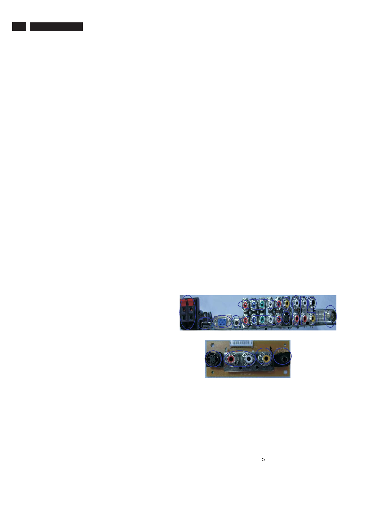
1.2 Connections
1.2.1Signal Connector(China model)
1 ). Tuner: PAL D/K for China model
Multi-standard for WE model
2 ) SPDIF OUT : Digital audio output (HDMI audio output)
3 ). PVR OUT : Composite video output (CVBS) and audio
R/L(RCA jack)
4 ). AV audio IN : AV1 and S-Video audio R/L(RCAjack)
5 ). AV1 IN : Composite video input (AV1)
6 ). S-Video 1 IN : S-video input (S-Video 1)
7 ). Comp video 1 IN : HDTV input with YPbPr format with audio R/L.
8 ). Comp video 2 IN : HDTV input with YPbPr format with audio R/L.
9 ). PC audio IN: audio R/L(mini-jack).
10). PC IN: VGA input (D-SUB connectors)
11). HDMI : digital video and audio input
12). speaker output : external speakers output connectors
13). earphone : earphone jack
14). AV2 IN : Composite video input (AV2 side)
15). AV audio IN : AV2 and S-Video side audio R/L(RCA jack)
16). S-Video IN : S-video input (S-Video side)
12
7
11
910
8
5
6
Fig1-1
2
4
1
3
1.1.
3 Miscellaneous
Power supply:
AC-input : 90V ~ 264VAC,
_
+
50/60 2Hz
Power consumption : 170W/Max(at PC mode),170W/
Max(at TV mode) with Audio
250W/Max(at PC mode),250W/
Max(at TV mode) with Audio(42")
Auto power saving : < 2W
Power cord length : 1.8M
Power cord type : European type and China type
Power indicator : LED (On: Blue ,Sleeping
mode: Amber )
(37")
1516
Fig1-2
1.2.2 Input signal
1.2.2.1 Signal type
1.2.2.1.1PC mode signal type:
a.Analog Video: 15 pin D-sub ,0.7 Vp-p linear, positive
polarity&separate sync.( TTL level, positive
or negative polarity)
b.Audio signal : 3.5mm stereo mini-jack
Level: Nominal : 0.5 V rms.
- Maximum : 1.5 V rms.
-Impedance > 10 k .
c.Signal source: Pattern generator format as attachment table
1to12.
Reference generator: CHROMA 2200 or QuantumData 802R
14
13

1. Technical Specifications and Connections
1.2.2.1.2TV mode signal type
RF Signal : Aerial input / 10mV(30-100dBuV)
Video signal : CVBS input ( RCA jack) / 1Vpp (300mV-sync,
700mV-video.)
S video input / 1VppY-signal, +/-300mV C-signal
SCART input: CVBS
Comp video in(YPbPr input)/ 1Vpp Y signal, +/-350mV Pb,Pr signal
HDMI:Digital interface with 4 channels TMDS signal
CVBS output ( RCA jack) / 1Vpp (300mV-sync, 700mV-video.)
Audio signal : Audio (1) R/L for AV IN(AV and S-Video).
Level: - Nominal : 0.5 V rms.
Audio (2) R/L for SCART IN
Level: - Nominal : 0.5 V rms.
Audio (3) R/L for Comp video IN.
Level: - Nominal : 0.5 V rms.
Audio (4) digital audio for HDMI Video IN.
1.2.2.1.3 PVR (CVBS) output:
Video: CVBS output 1Vpp / Impedance : 75
Audio: R/L output (from CVBS)
Level: - Nominal : 0.5 V rms.
- Maximum : 1.5 V rms.
- Impedance < 1 k
1.2.2.1.4 Scart output: ( for WE model only)
Video: CVBS output 1Vpp / Impedance : 75
Audio: R/L output (from CVBS)
Level: - Nominal : 0.5 V rms.
- Maximum : 1.5 V rms.
- Impedance < 1 k
1.2.2.1.5 SPDIF output: Serial digital audio output when input is HDMI.
1.2.2.1.6 Headphone
Audio: R/L output -10mW at 32
3.5mm stereo jack with switch
Impedance is between 8 and 600
1.2.2.2 TV system signal mode:
RF support:
China : PAL(D,K)
WE : PAL and SECAM(France).
CVBS/S-video: Support PAL, NTSC and SECAM colour system.
Comp video IN(YpbPr) : SDTV and HDTV, including 480i/p, 576i/p,
HDMI IN : 480P, 576P ,720P/50Hz , 720P/60Hz , 1080i/50Hz ,
1080i/60Hz
PVR (CVBS out) : Support PAL, NTSC and SECAM colour system.
1.2.2.3 Signal cab le
1.2.2.3.1 VGA s ignal cable
The input signals are applied to display through D-sub cable.
Length: 1.8 M +/- 50 mm (fixed)
Connector type: D-sub male.
15-pin D-sub VGA connector of the signal cable:
S SRGB signal ( for WE model only)
- Maximum : 1.5 V rms.
- Impedance > 10 k
- Maximum : 1.5 V rms.
- Impedance > 10 k
-Maximum : 1.5 V rms.
- Impedance > 10 k
.
.
.
720p 50/60Hz, 1080i 50/60Hz.
With DDC_2B pin assignments.
Blue connector thumb-operated jackscrews
.
.
.
.
.
.
TPT1.0A LA
1 Red video input
2 Green video input /SOG
3 Blue video input
4 GND
5 GND- cable detect
6 Red video ground
7 Green video ground
8 Blue video ground
9 DDC +3.3V (or 5V)
10 Logic ground
11 GND
12 Serial data line (SDA)
13 H. Sync / H+V
14 V. Sync
15 Data clock line (SCL)
1.2.2.3.2 HDMI for digital Video / Audio interface with pin assignment
as follows:
Pin No. Description
1RX2+
2GND
3RX2-
4RX1+
5GND
6RX1-
7RX0+
8GND
9RX0-
10 RXC+
11 GND
12 RXC-
13 CEC
14 NC
15 DDC clock
16 DDC data
17 GND
18 +5V POWER
19 Hot Plug Detect
1.2.2.3.3 CVBS
The input signals are applied to display through CVBS cable
Pin assignment
PIN NO. SIGNAL
1GND
2 CVBS
3 CVBS
4 CVBS
1.2.2.3.4 S-Video
The input signals are applied to display through S-Video cable
Pin assignment
PIN NO. SIGNAL
1GND
2GND
3GND
4GND
5GND
6LUMA
8 CHROMA
3

4
1.2.2.3.5 Component Video
1.2.2.3.6 SCART
TPT1.0A LA
The input signals are applied to display through Component
Video RCA Jack pin assignment
PIN NO. SIGNAL
1GND
2Redà Pr
3GND
4Blueà Pb
5GND
6GreenàY
Scart connector is only used in WE model. The Scart (Syndicat
des Constructeurs d'Appareils Radiorécepteurs et Televiseurs)
connector is used for combined audio and video connections.
1. Technical Specifications and Connections
Pin TV SCART
1 N/C
2 Right audio input
3 N/C
4 Audio ground
5 Blue ground
6 Left audio input
7 Blue output
8
0-2.5 volts (low) when:
TV output
4.5-7.5 volts (High-t o-6v) when :
-inputting picture format setting is '16:9',
9-12 volts (high -to-12v) wh en:
-inputing picture format setting is '4:3'
9 Green ground
10 N/C
11 Green output
12 N/C
13 Red ground
14 N/C
15 Red output
16
0volt (low)when:-pin8oftheTVscartis
low
or when:
- Composite video signal
1-3 volts (high ) when:
- video input setting is 'RGB',
17 Composite video output ground
18 Composite video input ground
19 N/C
20 Composite video input
21 Ground

2. Safety Instructions, Warnings and Notes
2. Safety Instructions, Warnings and Notes
TPT1.0A LA
5
index of this chapter:
2.1 Safety Instructions
2.2 Warnings
2.3 Notes
2.1 Safety Instructions
Safety regulations require that during a repair:
·
Connect the set to the AC Power via an isolation
transformer (> 800 VA).
·
Replace safety components, indicated by the symbol ,
only by components identical to the original ones. Any
other component substitution (other than original type) may
increase risk of fire or electrical shock hazard.
Safety regulations require that after a repair, the set must be
returned in its original condition. Pay in particular attention to
the following points:
·
Route the wire trees correctly and fix them with the
mounted cable clamps.
·
Check the insulation of the AC Power lead for external
damage.
·
Check the strain relief of the AC Power cord for proper
function.
·
Check the electrical DC resistance between the AC Power
plug and the secondary side (only for sets which have a AC
·
Power isolated power supply):
1. Unplug the AC Power cord and connect a wire
between the two pins of the AC Power plug.
2. Set the AC Power switch to the "on" position (keep the
AC Power cord unplugged!).
3. Measure the resistance value between the pins of the
AC Power plug and the metal shielding of the tuner or
the aerial connection on the set. The reading should be
between 4.5 Mohm and 12 Mohm.
4. Switch "off" the set, and remove the wire between the
two pins of the AC Power plug.
·
Check the cabinet for defects, to avoid touching of any
inner parts by the customer.
2.2 Warnings
·
All ICs and many other semiconductors are susceptible to
electrostatic discharges (ESD ). Careless handling
during repair can reduce life drastically. Make sure that,
during repair, you are connected with the same potential as
the mass of the set by a wristband with resistance. Keep
components and tools also at this same potential.
·
Be careful during measurements in the high voltage
section.
·
Never replace modules or other components while the unit
is switched "on".
·
When you align the set, use plastic rather than metal tools.
This will prevent any short circuits and the danger of a
circuit becoming unstable.
2.3 Notes
2.3.1 General
··
Measure the voltages and waveforms with regard to the
chassis (= tuner) ground ( ), or hot ground ( ), depending
on the tested area of circuitry. The voltages and waveforms
shown in the diagrams are indicative. Measure them in the
Service Default Mode (see chapter 5) with a color bar
signal and stereo sound (L: 3 kHz, R: 1 kHz unless stated
otherwise) and picture carrier at 475.25 MHz for PAL, or
61.25 MHz for NTSC (channel 3).
··
Where necessary, measure the waveforms and voltages
with ( ) and without ( ) aerial signal. Measure the
voltages in the power supply section both in normal
operation ( ) and in stand-by ( ). These values are
indicated by means of the appropriate symbols.
The semiconductors indicated in the circuit diagram and in
··
the parts lists, are interchangeable per position with the
semiconductors in the unit, irrespective of the type
indication on these semiconductors.
·
Manufactured under license from Dolby Laboratories.
"Dolby" and the "double-D symbol", are trademarks of
Dolby Laboratories.
2.3.2 Schematic Notes
All resistor values are in ohms and the value multiplier is
·
often used to indicate the decimal point location (e.g. 2K2
indicates 2.2 kohm).
Resistor values with no multiplier may be indicated with
·
either an "E" or an "R" (e.g. 220E or 220R indicates 220
ohm).
All capacitor values are given in micro-farads (u= x10 ),
·
nano-farads (n= x10 ), or pico-farads (p= x10 ).
·
Capacitor values may also use the value multiplier as the
decimal point indication (e.g. 2p2 indicates 2.2 pF).
An "asterisk" (*) indicates component usage varies. Refer
·
to the diversity tables for the correct values.
·
The correct component values are listed in the Electrical
Replacement Parts List. Therefore, always check this list
when there is any doubt.
-9
-12
-6
2.3.3 Rework on BGA (Ball Grid Array) Ics
General
Although (LF)BGA assembly yields are very high, there may still be
a requirement for component rework. By rework, we mean the
process of removing the component from the PWB and replacing it
with a new component. If an (LF)BGA is removed from a PWB, the
solder balls of the component are deformed drastically so the
removed (LF)BGA has to be discarded.
Device Removal
As is the case with any component that, it is essential when
removing an (LF)BGA, the board, tracks, solder lands, or
surrounding components are not damaged. To remove an(LF)BGA,
the board must be uniformly heated to a temperature close to the
reflow soldering temperature. A uniform temperature reduces the
chance of warping the PWB.To do this, we recommend that the
board is heated until it is certain that all the joints are molten.
Then carefully pull the component off the board with a vacuum
nozzle. For the appropriate temperature profiles, see the IC data
sheet.
Area Preparation
When the component has been removed, the vacant IC area must
be cleaned before replacing the (LF)BGA.Removing an IC often
leaves varying amounts of solder on the mounting lands. This
excessive solder can be removed with either a solder sucker or
solder wick. The remaining flux can be removed with a brush and
cleaning agent.After the board is properly cleaned and inspected,
apply flux on the solder lands and on the connection balls of
the (LF)BGA.
Note: Do not apply solder paste, as this has shown to result in
problems during re-soldering.
Device Replacement
The last step in the repair process is to solder the new component
on the board. Ideally, the (LF)BGAshould be aligned under a
microscope or magnifying glass. If this is not possible, try to align
the (LF)BGA with any board markers. To reflow the solder, apply a
temperature profile according to the IC data sheet. So as not to
damage neighbouring components, it may be necessary to reduce
some temperatures and times.
More Information
For more information on how to handle BGA devices, visit this
URL: (needs subscription,
www.atyourservice.ce.philips.com
not available for all regions). After login, "select Magazine", then
go to "Workshop Information". Here you will find Information on
how to deal with BGA-ICs.

6
TPT1.0A LA
2. Safety Instructions, Warnings and Notes
2.3.4 Lead Free Solder
Philips CE is going to produce lead-free sets (PBF) from
1.1.2005 onwards.
Lead-free sets will be indicated by the PHILIPS-lead-free logo
on the Printed Wiring Boards (PWB):
In case of doubt whether the board is lead-free or not (or with
mixed technologies), you can use the following method:
·
Always use the highest temperature to solder, when using
SAC305 (see also instructions below).
·
De-solder thoroughly (clean solder joints to avoid mix of
two alloys).
Caution must
which is coupled to the 12NC. For an overview of these
profiles, visit the website
(needs subscription, but is not available for all regions)
You will find this and more technical information within the
"Magazine", chapter "Workshop information".
For additional questions please contact your local repair help
desk.
: For BGA-ICs, you use the correct temperatureprofile,
www.atyourservice.ce.philips.com
Fig 2-1 Lead-free logo
This sign normally has a diameter of 6 mm, but if there is less
space on a board also 3 mm is possible.
In case of doubt wether the board is lead-free or not (or with
mixed technologies), you can use the following method:
·
Always use the highest temperature to solder, when using
SAC305 (see also instructions below).
·
De-solder thoroughly (clean solder joints to avoid mix of
two alloys).
Caution
which is coupled to the 12NC. For an overview of these
profiles, visit the website
(needs subscription, but is not available for all regions)
You will find this and more technical information within the
"Magazine", chapter "Workshop information".
For additional questions please contact your local repairhelpdesk.
Due to lead-free technology some rules have to be respected
by the workshop during a repair:
·
is required,please contact the manufacturer of your soldering
equipment. In general, use of solder paste within
workshops should be avoided because paste is not easy to
store and to handle.
soldering tin. The solder tool must be able
-To reach at least a solder-tip temperature of 400 C.
-To stabilise the adjusted temperature at the solder-tip.
-To exchange solder-tips for different applications.
·
- 380 C is reached and stabilised at the solder joint.
Heating time of the solder-joint should not exceed~4sec.
Avoid temperatures above 400 C, otherwise wear-out of
tips will rise drastically and flux-fluid will be destroyed. To
avoid wear-out of tips, switch "off" unused equipment or
reduce heat.
·
tin/parts is possible but PHILIPS recommends strongly to
avoid mixed regimes. If not to avoid, clean carefully the
solder-joint from old tin and re-solder with new tin.
Not listed standard material (commodities) has to be
purchased at external companies.
delivered in so-called "dry-packaging" to protect the IC
against moisture. This packaging may only be opened
short before it is used (soldered). Otherwise the body of the
IC gets "wet" inside and during the heating time the
structure of the IC will be destroyed due to high (steam-)
pressure inside the body. If the packaging was opened
before usage, the IC has to be heated up for some hours
(around 90C)fordrying (think of ESD-protection !).
Do not re-use BGAs at all!
·
soldering tin and components, all needed spare parts will
be available till the end of the service period. For the repair
of such sets nothing changes.
: For BGA-ICs, you must use the correct temperatureprofile,
www.atyourservice.ce.philips.com
Use only lead-free soldering tin . If lead-free solder paste
·
Use only adequate solder tools applicable for lead-free
Adjust your solder tool so that a temperature around 360 C
Mix of lead-free soldering tin/parts with leaded soldering
Use only original spare-parts listed in the Service-Manuals.
·
·
Special information for lead-free BGAICs: these ICs will be
For sets produced before 1.1.2005, containing leaded
2.3.5 Practical Service Precautions
·
It makes sense to avoid exposure to electrical shock.
While some sources are expected to have a possible
dangerous impact, others of quite high potential are of
limited current and are sometimes held in less regard.
·
Always respect voltages.
dangerous in themselves, they can cause unexpected
reactions - reactions that are best avoided. Before reaching
into a powered TV set, it is best to test the high voltage
insulation. It is easy to do, and is a good service precaution.
While some may not be

3. Directions for Use
3. Directions for Use
You can download this information from the following websites:
http://www.philips.com/support
http://www.p4c.philips.com
TPT1.0A LA
7

8
TPT1.0A LA
4. Mechanical Instructions
Index of this chapter:
4.1 Assy/Panel Removal
4.2 Set Re-assembly
4.1 Assy/Panel Removal
Front view
Back view
4. Mechanical Instructions
Fig.5
Step 3. Remove IR, Side AV, Key board and Main shield assy as Fig.6~8.
a. Remove the 4 screws to remove the as Fig.6
b. Remove the 1 cable and 2 screws to remove Side AV board as Fig.7
c. Remove the 1 cable and 2 screws to remove IR board as Fig.7
d. Remove the 1 cable to remove Key board as Fig.7
e. Remove the the other 2 cables and 6 screws to remove the Main
shield assy as Fig.7~8
Fig.1
Fig.2
Step 1. Remove the stand and speaker.
a. Remove the 2 screws to remove the stand as Fig.3
Fig.3
b. Remove the 4 screws and 2 cables to remove the speaker as Fig.4
Fig.6
Fig.7
Fig.8
Step 4. Remove the Scaler and Power board.
a. Remove the 11 screws as Fig. 9
b. Remove the 12 screws to remove the Scaler and Power board as
Fig10~11
Step 2. Remove the Back cover as Fig.5.
Remove the 20 screws to remove the Back cover as Fig.5
a.
Fig.9
Fig.4
Fig. 10
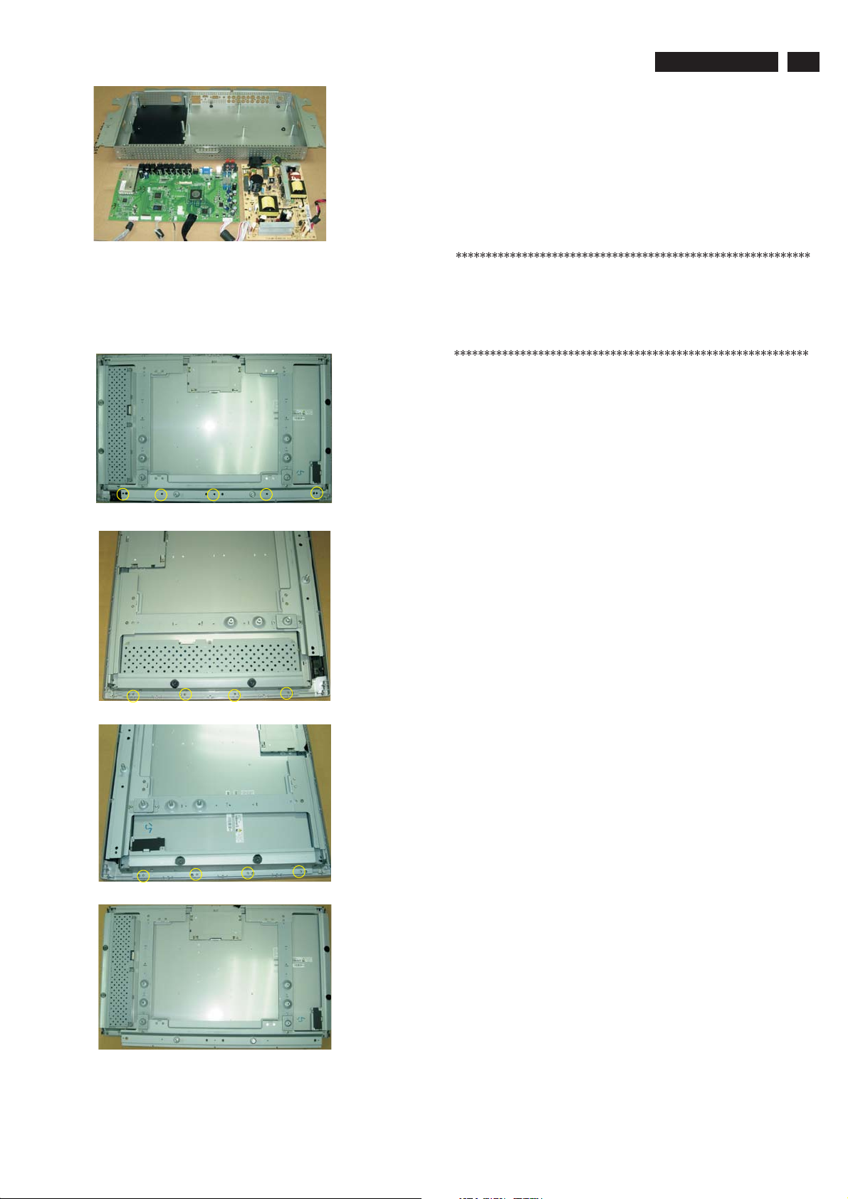
4. Mechanical Instructions
4.2 Set Re-assembly
To re-assemble the whole set, execute all processes in reverse
order.
Notes:
a. While re-assembling, make sure that all cables are placed
and connected in their original position.
b. Pay special attention not to damage the EMC foams at the
SSB shielding. Check that EMC foams are put correctly on
Fig. 11
their places.
TPT1.0A LA
9
Step 5. Remove the Bezel assy as Fig.12~Fig.15 .
Remove the 5 screws
a. as Fig.12
b. Remove the 4 screws as Fig.13
c. Remove the 4 screws as Fig.14
d . as Fig.15
Remove the Bezel assy
In warranty, it is not allowed to disassembly the LCD panel, even the
backlight unit defect.
Out of warranty, the replacment of backlight unit is a correct way
when the defect is cused by backlight (CCFL,Lamp).
Fig. 12
Fig. 13
Fig. 14
Fig. 15
10
TPT1.0A LA
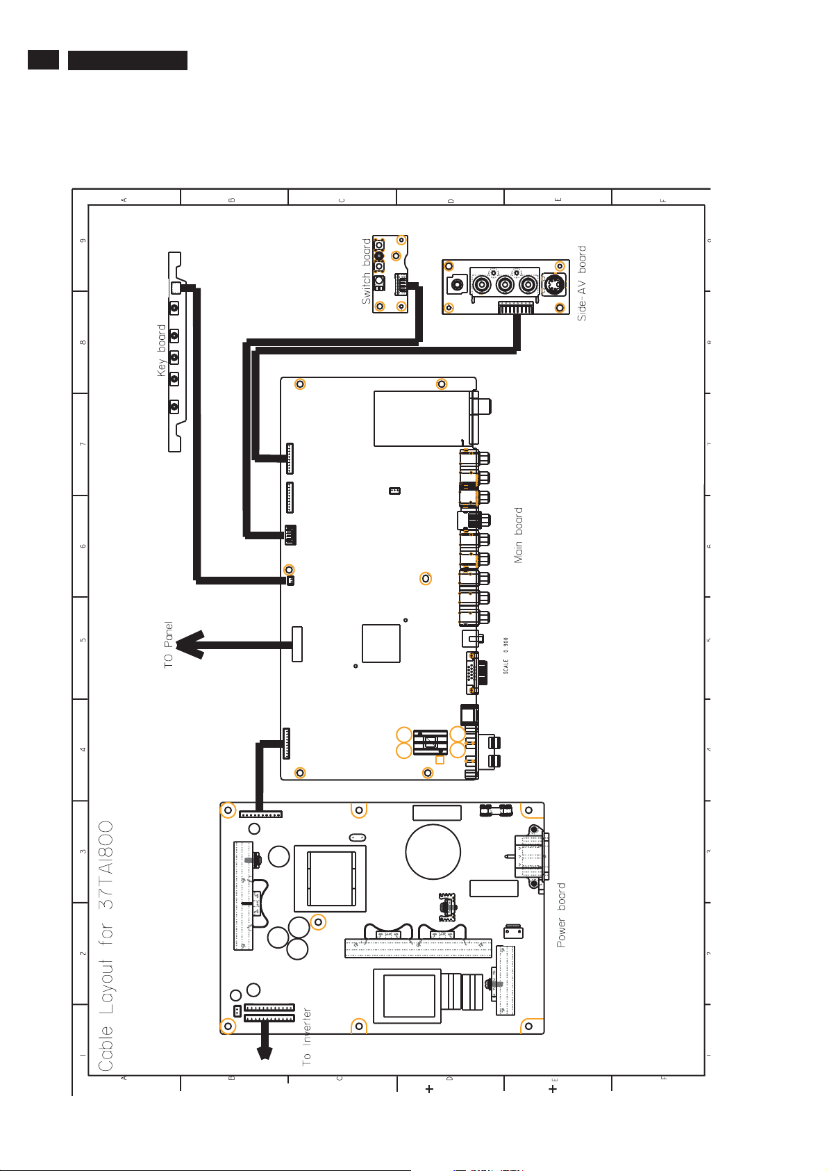
5. Block Diagram
Index of this chapter:
5.1
Wiring Diagram
5.2 Block Diagram
5.1 Wiring Diagram
5. Block Diagram
3138 14723781
3138 14723781
PHILIPS
PHILIPS
COMPONENT SIDE
8P
16308P1630
1
8
COMPONENT
1
2P
2
1921 2P1921
10
10PIN
10PIN
CN109
CN109
1
6
6PIN
6PIN
CN114
CN114
1
2
2PIN
2PIN
CN113
CN113
1
1
6P
19076P1907
6
3
1
CN112
CN112
3PIN
3PIN
10
CN117
CN117
10PIN
10PIN
COMPONENT SIDE
1
1089 10P1089 10P
1
10
1064
1063 12P1063 12P
1
1071
1
12
1088 12P1088 12P
12
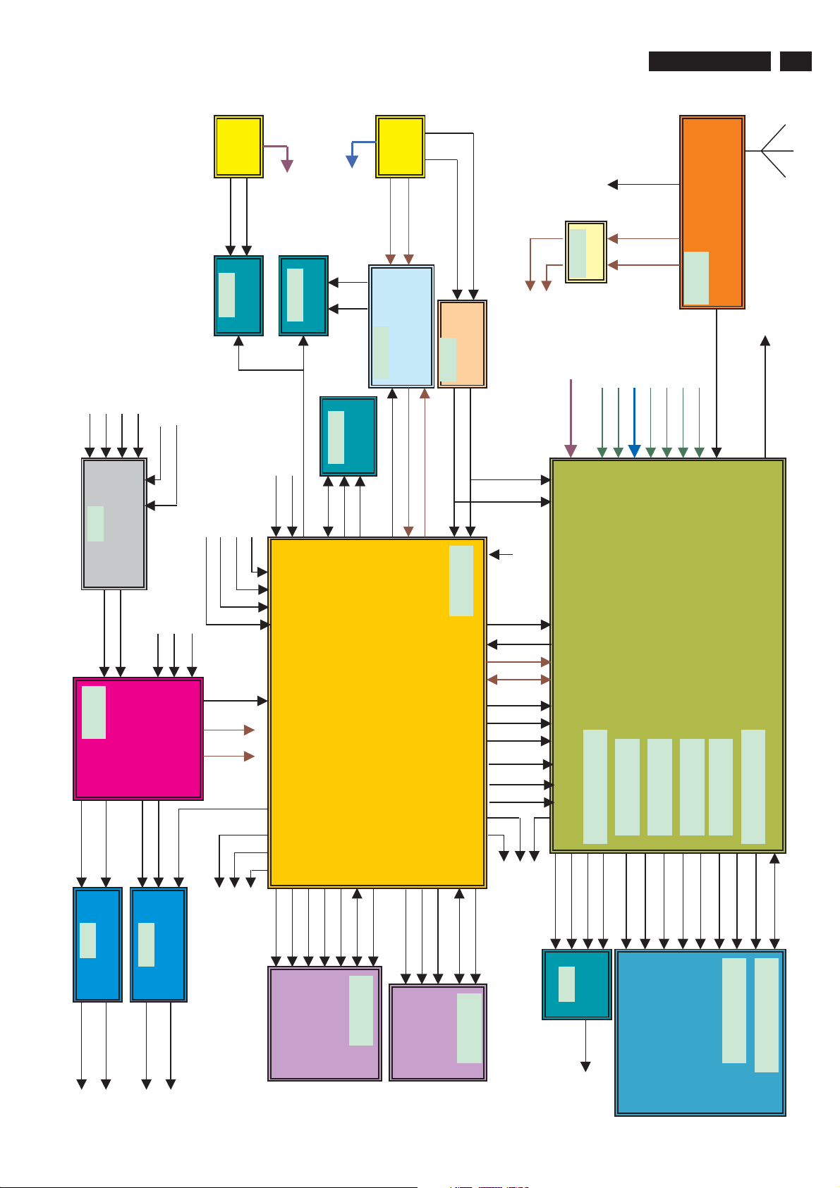
5.2 Block Diagram
Connector
HDMI
5. Block Diagram
Function block of scaler Board
Connector
DSUB
TPT1.0A LA
11
COMP1 R/L
COMP2 R/L
DSUB R/L
HDMI R/L
74HC4052D
+5V
SC3_IN_R
SC3_IN_L
SW4
CVBS2 R/L
SW3
CVBS1 R/L
SIF_OUT
RX5V1_DD
C_SCL
5V_SB
REMOTE_3V
HP_DET
KEYA
HDMI1_RX0/
1/2/3/C+-
RX5V1_DD
C_SDA
M24C02
POWER_ON
DDC_5V
HDMI_HOTPLUG
DETECT_VGA
PC_R/G/BIN
M24C02
SDA
SCL
24LC64
3.3V_SB
DDC_WP
SDAE
SCLE
DDCSDA
74LV4053PW
DDC_5V
ISP_SW
E_PAGE
DDCSCL
RX
TX
VGA_VSIN
VGA_HSIN
74LVC14ADT
5V_SB
PC_HSIN
PC_VSIN
PC_HSIN
PC_VSIN
3.3V_SB
3V_SDA
3V_SCL
1/2/3/C+-
CPU_RESET
PCA9512
3.3V_SB
HDMI1_RX0/
YPbPr1_Y/Pb/Pr
YPbPr2_Y/Pb/Pr
5V_SDA
5V_SCL
SIF_OUT
SV1_Y/C_MP
SV2_Y/C_MP
PC_R/G/BIN
CVBS2_MP
SVP-PX66
FQ1256
+5V
CVBS1_MP
TV_CVBS
HDMI_SPDIF
+5V
MSP3410G
HP_R_OUT
HP_L_OUT
TDA1308T
+5V
HP_ROUT
HP_LOUT
AR_DACM
AL_DACM
TPA3008D2
+16V
ROUT+/-
LOUT+/-
MSP_INT
5V_SDA
5V_SCL
SOUND_EN
SB_PWR
PANEL_PWR
INVERTER_ON_OFF
CPU_RESET
8051_RD#
8051_WR#
RY_BY
SST39VF088
FLASH
M30620SPGP
SRAM_ENABLE
8051_RD#
(NI)
for TT
8051_WR#
AD0-AD7
IS61LV256-12T
3.3V_SB
SRAM
AD0-AD7
A0-A19
CE#
3.3V_SB
RESET_H
PX_INT#
3V_SCL
3V_SDA
8051_ALE
8051_WR#
8051_RD#
8051_CS2PX
8051_A0-7
8051_AD0-7
SW4
SW3
A0-A14
PX_HMMI33
HDMI_MCLK
BRIGHT_ADJ
HDMI_SD0
CS4344
+5V
PX_VL18
PX_MCK0/0#
HDMI_SCK
HDMI_WS
PX_VD33
PX_VA18
PX_RAS#/CAS#
PX_CS0#
PX_WE#
PX_CLKE
K4D263238G-VC33
(2.5V)
DDR
PX_VDDMQ
PX_VD18
PX_DQS0-3
PX_MA0-11
PX_BA0-1
PX_VDDMQ
PX_VDDM
PX_MD0-31
12
TPT1.0A LA
90 ~ 264V
AC Input
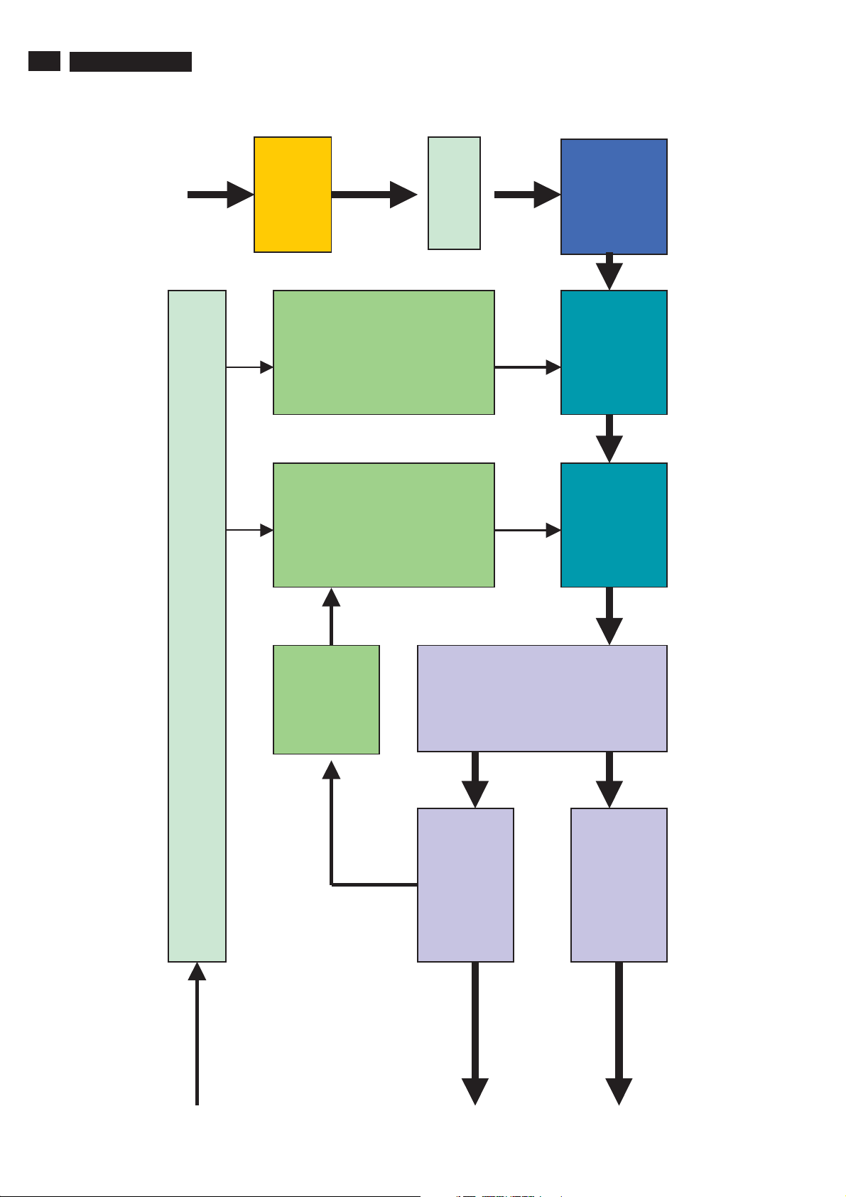
5. Block Diagram
Function block of power Board
AC Inlet
TCET1103(G)
Photo-coupler
FILTER
EMI
AC to DC
KBU8J
STW26NM60
PFC control
L6562 &
Control interface
Feedback
Protect /
network
TCET1103(G)
Photo-coupler
MBRF10H100CT
AC to DC
Transformer
EQ40
STW18NK80Z
PWM control
TEA1507P &
AC to DC
STPS40H100CW
Control from
scalerboard
16V 2.5A
Panel/scalar/
Audio
24V 7A_37”
Inverter board
24V 9A_42”
6.Circuit Diagram & PWB Layouts
Index of this chapter:
6.1 Chassis Overview
6.2 Exploded View
6.3 Scaler Board Schematic Diagram & Layouts
6.4 Power Board Schematic Diagram & Layouts
6.5 SIDE AV Schematic Diagram & Layouts
6.6 IR Schematic Diagram & Layouts
6.7 KEY Schematic Diagram & Layouts
Board
Board
Board
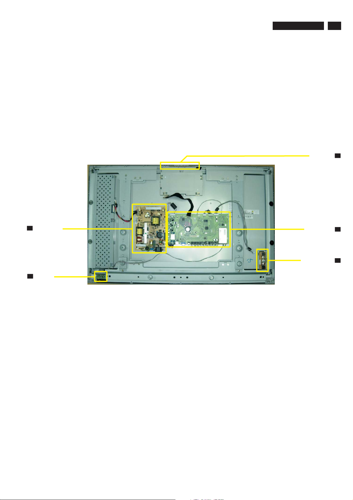
6.1 Chassi Overview
TPT1.0A LA
13
Power Board
P
I
IR Board
Key Board
Scaler Board
Side AV Board
K
S
A

14
6.2 37 Exploded View"
090
313815761281
MAIN SHIELD ASSY
TPT1.0A LA
6.Circuit Diagram & PWB Layouts
40
313815761291
BACK COVER ASSY
1054
313815864961
POWER PCB ASSY
1053
996500039547
SCALER BOARD_VISION-D
1050
823827720921
CPT CLAA370WA03
1055
96500039542
SIDE_AV_BOARD_VISION_D
BASE ASSY
313815761451
IR ASSY
996500039543
1056
996500039544
313815761441
FRONT BEZEL ASSY
1057
KEY BOARD

6.3.1 Scaler Schematic Diagram-ContentsBoard
S-01
6.Circuit Diagrams and PWB Layouts
TPT1.0A LA
15

16
TPT1.0A LA
6.3.2 Scaler Schematic Diagram - DSUB/DVIBoard
S-02
6. Circuit Diagrams and PWB Layouts

6.3.3 Scaler Schematic Diagram - HDMIBoard
S-03
6.Circuit Diagrams and PWB Layouts
TPT1.0A LA
17

18
TPT1.0A LA
6.3.4 Scaler Schematic Diagram - TUNNERBoard
S-04
6. Circuit Diagrams and PWB Layouts

6.3.5 Scaler Schematic Diagram - AV CONNECTORBoard
S-05
6.Circuit Diagrams and PWB Layouts
TPT1.0A LA
19
20
TPT1.0A LA
6.3.6 Scaler Schematic Diagram - IOBoard
S-06
6. Circuit Diagrams and PWB Layouts
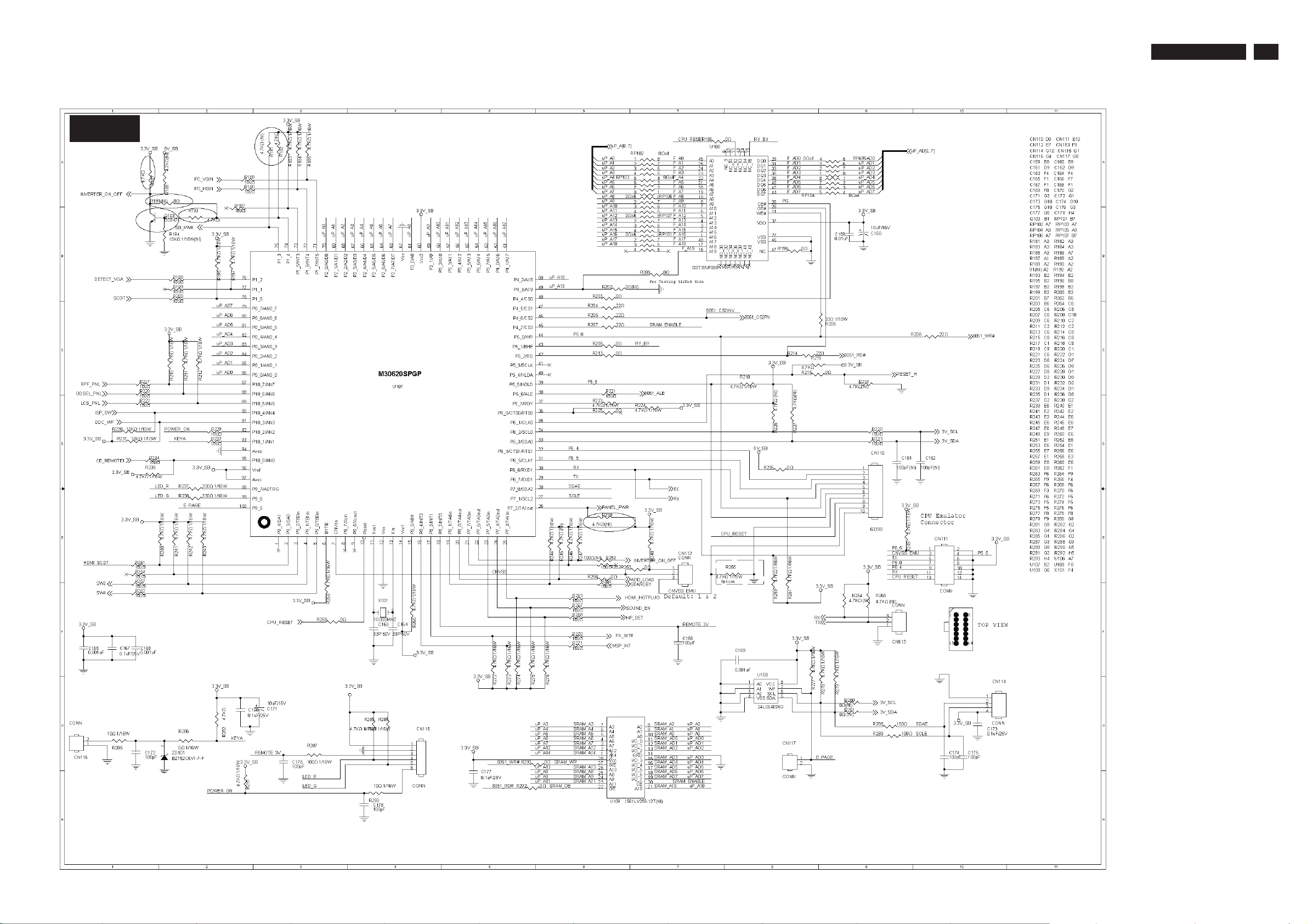
6.3.7 Scaler Schematic Diagram - CPU M30620SPGPBoard
S-07
6.Circuit Diagrams and PWB Layouts
TPT1.0A LA
21

22
TPT1.0A LA
6.3.8 Scaler Schematic Diagram - SVP-PX66-1Board
S-08
6. Circuit Diagrams and PWB Layouts
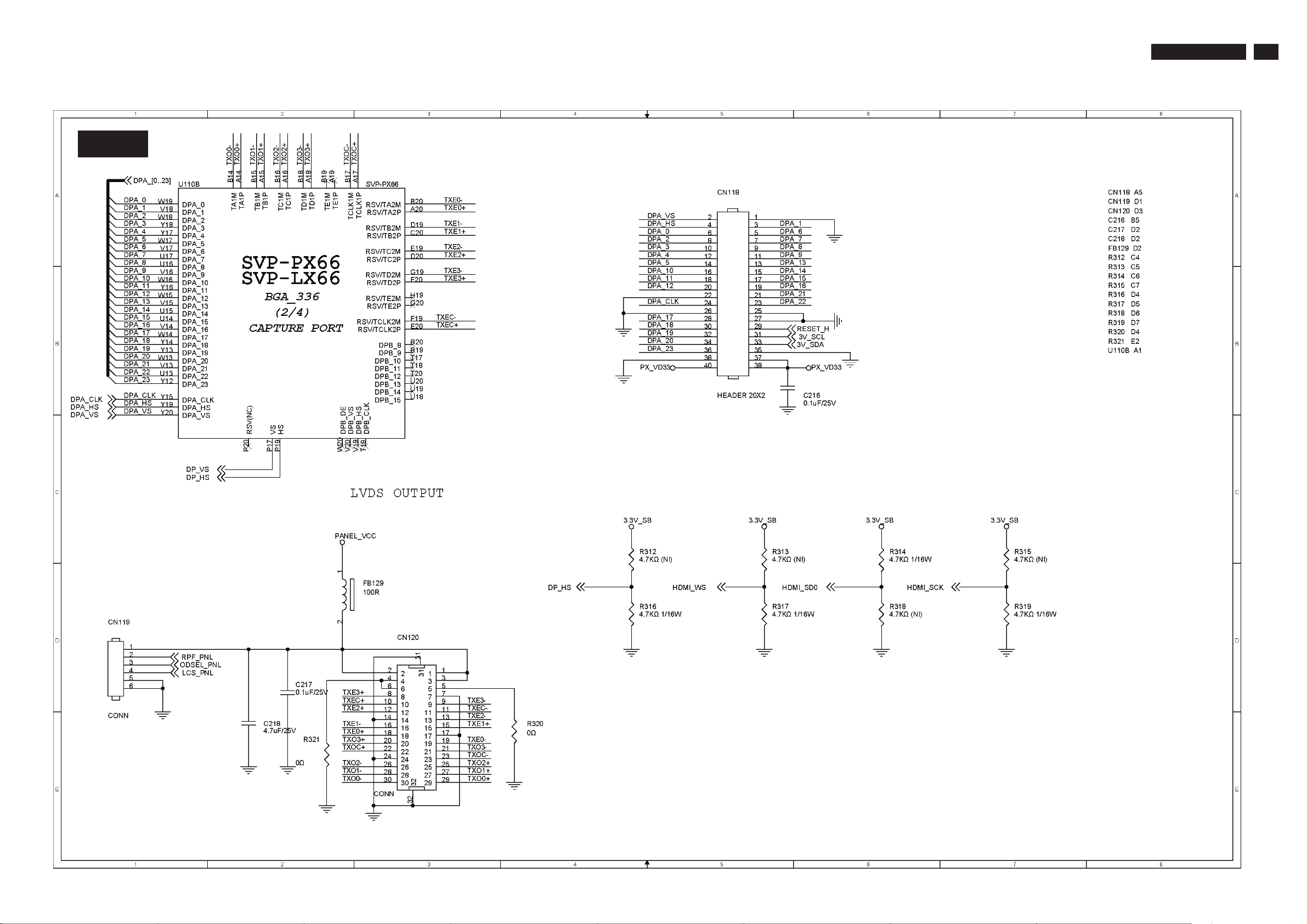
6.3.9 Scaler Schematic Diagram - SVP-PX66-2Board
S-09
6.Circuit Diagrams and PWB Layouts
TPT1.0A LA
23

24
TPT1.0A LA
6.3.10 Scaler Schematic Diagram - SVP-PX66-3Board
6. Circuit Diagrams and PWB Layouts
S-10

6.3.11 Scaler Schematic Diagram - SVP-PX66-4Board
S-11
6.Circuit Diagrams and PWB Layouts
TPT1.0A LA
25
26
TPT1.0A LA
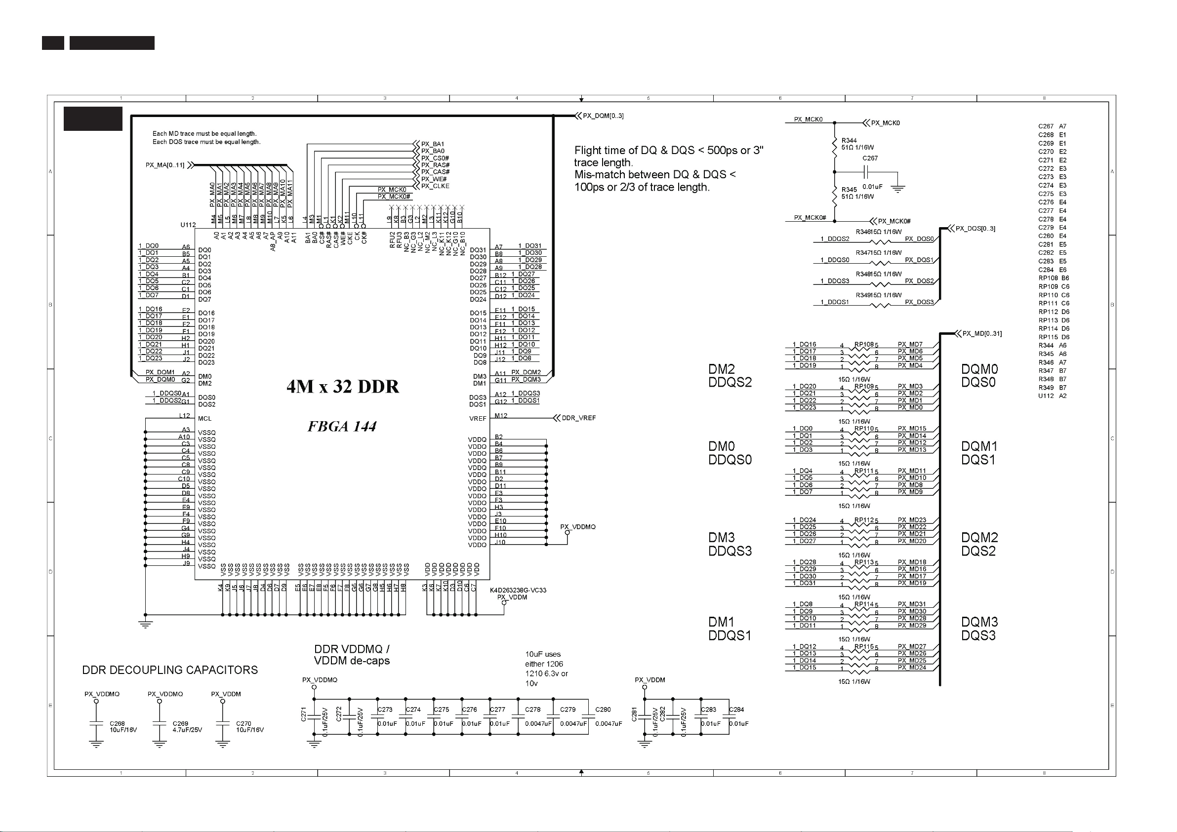
6.3.12 Scaler Schematic Diagram - DDR 4Mx32Board
S-12
6. Circuit Diagrams and PWB Layouts

6.3.13 Scaler Schematic Diagram - SOUND DELAYBoard
S-13
6.Circuit Diagrams and PWB Layouts
TPT1.0A LA
27

28
TPT1.0A LA
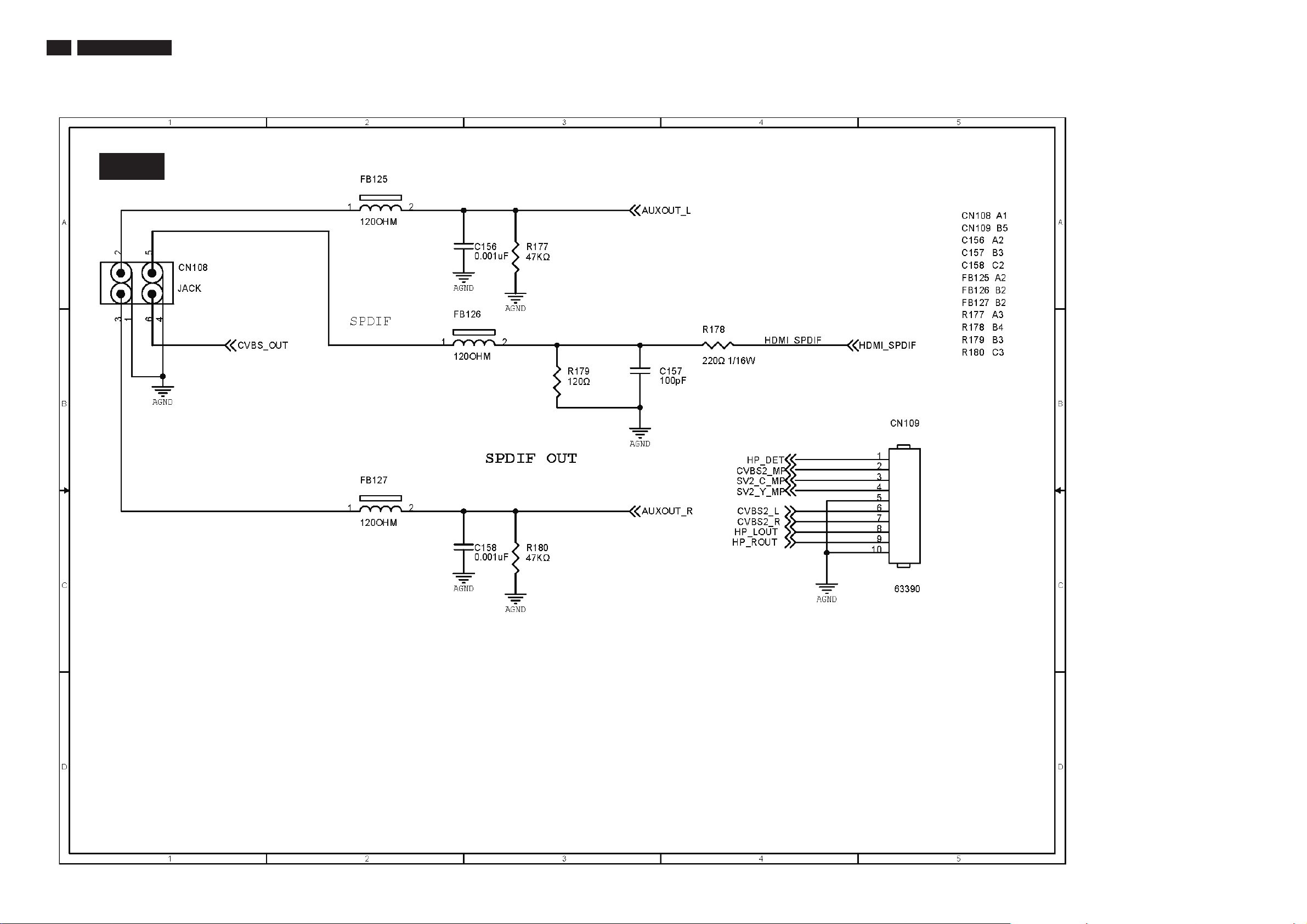
6.3.14 Scaler Schematic Diagram - AUDIO DECODERBoard
S-14
7. Circuit Diagrams and PWB Layouts

6.3.15 Scaler Schematic Diagram - AUDIO AMPBoard
S-15
6.Circuit Diagrams and PWB Layouts
TPT1.0A LA
29

30
TPT1.0A LA
6.3.16 Scaler Schematic Diagram - POWER 1Board
S-16
6. Circuit Diagrams and PWB Layouts

6.3.17 Scaler Schematic Diagram - POWER2Board
S-17
6.Circuit Diagrams and PWB Layouts
TPT1.0A LA
31

32
TPT1.0A LA
6.3.18 Scaler Schematic Diagram - RESETBoard
S-18
6. Circuit Diagrams and PWB Layouts

6.3.19 Scaler Board Layouts-1
S-19S-19
6.Circuit Diagrams and PWB Layouts
TPT1.0A LA
33

34
TPT1.0A LA
6.3.20 Scaler Board Layouts - 2
S-20
6. Circuit Diagrams and PWB Layouts

6.4 Power Board Schematic Diagram(37 )"
P
6.Circuit Diagrams and PWB Layouts
TPT1.0A LA
35

36
TPT1.0A LA
6.4 Power Board Layouts - 1(37")
P
6. Circuit Diagrams and PWB Layouts

6.4 Power Board Layouts - 2(37")
P
6.Circuit Diagrams and PWB Layouts
TPT1.0A LA
37

38
6.5 Side AV Board Schematic Diagram
TPT1.0A LA
6. Circuit Diagrams and PWB Layouts

6.5 SIDE AV Board Layouts-1
A
6.Circuit Diagram & PWB Layouts
TPT1.0A LA
39

40
6.5 SIDE AV Board Layouts-2
TPT1.0A LA
A
6. Circuit Diagrams and PWB Layouts

6.6 IR Board Schematic Diagram
6.Circuit Diagram & PWB Layouts
TPT1.0A LA
41

42
6.6 IR Board Layouts-1
TPT1.0A LA
I
6. Circuit Diagrams and PWB Layouts

6.6 IR Board Layouts-2
I
6.Circuit Diagram & PWB Layouts
TPT1.0A LA
43

44
6.7 KEY Board Schematic Diagram
TPT1.0A LA
6. Circuit Diagrams and PWB Layouts

6.Circuit Diagram & PWB Layouts
TPT1.0A LA
45
6.7 KEY Board Layouts-1
K
6.7 KEY Board Layouts-2
K

46
TPT1.0A LA
7. Alignments
7. Alignments
Index of this chapter:
7.1 Electrical Instructions
7.2 Software Updrade With ISPWriter
7
.1 Electrical Instructions&Serial NO. Definition
1. General points
1.1 During the test and measuring, supply a distortion free AC mains
voltage to the apparatus via an isolated transformer with low
internal resistance.
1.2 All measurements mentioned hereafter are carried out at a normal
mains voltage (90 - 142 VAC for NAFTA version, 195 -264 VAC for
EUROPEAN version, or 90 - 264 VAC for the model with full range
power supply, unless otherwise stated.)
1.3 All voltages are to be measurement or applied with respect to
ground,unless otherwise stated.
1.4 The test has to be done on a complete set including LCD panel in
a room with temperature of 25 +/- 5 degree C.
1.5 All values mentioned in these test instruction are only applicable of
a well aligned apparatus, with correct signal.
1.6 The letters symbols (B) and (S) placed behind the test instruction
denotes
(B): carried out 100% inspection at assembly line
1.7 The white balance (color temperature), has to be tested in subdued
1.8 Repetitive power on/off cycle are allowed except it should be
2. Input and output signal
2.1.1 PC mode signal type
2.1.2 TV mode signal type
2.1.3 PVR (CVBS) output:
(S): carried out test by sampling
lighted room.
avoided within 6 sec.
a.Analog Video:15 pin D-sub ,0.7 Vp-p linear, positive polarity&
separate sync.( TTL level, positive or negative polarity)
b.Audio signal : 3.5mm stereo mini-jack
Level: Nominal : 0.5 V rms.
c.Signal source: Pattern generator format as attachment table
Reference generator : CHROMA 2200 or QuantumData 802R
RF Signal : Aerial input / 10mV(typical: 80dBuV; range:
30-100dBuV)
Video signal : CVBS input ( RCA jack) / 1Vpp (300mV-sync,
700mV-video.) S video input / 1VppY-signal, +/-300mV C-signal
SCART input: CVBS, S, SRGB signal ( for WE model only) Comp
video in(YPbPr input)/ 1Vpp Y signal, +/-350mV Pb,Pr signal
HDMI:Digital interface with 4 channels TMDS signal
CVBS output ( RCA jack) / 1Vpp (300mV-sync, 700mV-video.)
Audio signal : Audio (1) R/L for AV IN(AV and S-Video).
Audio (2) R/L for SCART IN
Audio (3) R/L for Comp Video IN.
Audio (4) digital audio for HDMI Video IN.
Video: CVBS output 1Vpp / Impedance : 75
Audio: R/L output (from CVBS)
Level: - Nominal : 0.5 V rms.
&Serial NO. Definition
- Maximum : 1.5 V rms.
-Impedance > 10 k
1to12.
Level: - Nominal : 0.5 V rms.
- Maximum : 1.5 V rms.
- Impedance > 10 k
Level: - Nominal : 0.5 V rms.
- Maximum : 1.5 V rms.
- Impedance > 10 k
Level: - Nominal : 0.5 V rms.
-Maximum : 1.5 V rms.
- Impedance > 10 k .
.
.
.
.
- Maximum : 1.5 V rms.
- Impedance < 1 k
2.1.4 Scart output: ( for WE model only)
Video: CVBS output 1Vpp / Impedance : 75
Audio: R/L output (from CVBS)
Level: - Nominal : 0.5 V rms.
- Maximum : 1.5 V rms.
- Impedance < 1 k
2.1.5 SPDIF output: Serial digital audio output when input is HDMI
2.1.6 Headphone
Audio: R/L output - 10mW at 32
3.5mm stereo jack with switch
Impedance is between 8 and 600
2.2 PC Input signal mode
2.2.1 PRESET VIDEO RESOLUTION
The analogue color LCD monitor must be capable of
displaying standard resolutions within the vertical
frequency range of 50 - 75 Hz, and horizontal scan
range of 30 - 63 KHz .
Use the CHROMA-2250 or QuantumData 802R
generator as the standard signal timing source.
Mode 3, 7, 8, 12, 15, 16 are preset modes that
should pass QA inspection.
Mode 1, 2, 4, 5, 6, 9, 10, 11, 13, 14 will run auto
adjustment only, and W/O QA
checking.
Table 1. PC timing table
Mode Resolution H. freq. / V. freq Standard
1. 640 x 350 31.469Khz/70.087Hz VGA
2. 720 x 400 31.469Khz/70.087Hz VGA
3. 640 x 480 31.469Khz/59.940Hz VGA
4. 640 x 480 35.000Khz/66.667Hz Macintosh
5. 640 x 480 37.861Khz/72.809Hz VESA
6. 640 x 480 37.500Khz/75.000Hz VESA
7. 800 x 600 35.156Khz/56.250Hz VESA
8. 800 x 600 37.879Khz/60.317Hz VESA
9. 800 x 600 48.077Khz/72.188Hz VESA
10. 800 x 600 46.875Khz/75.000Hz VESA
11. 832 x 624 49.700Khz/75.000Hz Macintosh
12. 1024 x 768 48.363Khz/60.004Hz VESA
13. 1024 x 768 56.476Khz/70.069Hz VESA
14. 1024 x 768 60.023Khz/75.029Hz VESA
15. 1280 x 720 44.772kHz/59.855 Hz CVT
16. 1280 x 768 47.776kHz/59.87Hz CVT
2.3 TV input signal Channel and pattern
2.3.1 TV Table 2. China model
Table 2. RF Signal Distribution Table (PAL)
.
.
.
.
.

7. Alignments
TPT1.0A LA
47
Frequency Carries
S/N CH
Video Sound
1 AU2 64.25 MHz
2 C8 184.25 MHz
AU10
3
4 S26 343.25 MHz
5 C13 471.25 MHz
6 I23 487.25 MHz
209.25 MHz
(E12)
69.75
MHz
190.75
MHz
214.75
MHz
349.25
MHz
477.75
MHz
493.25
MHz
Pattern
TV System
Picture
Color Bar +
PAL B/G (7M)
PAL D/K (8M) 100% White Mono 6.5
PAL B/G(7M) Philips Circle Mono 5.5 1KHz
PAL I (8M) 100% White + Circle Mono 6.0 Music 16 : 9
PAL D/K (8M)
PAL I (8M)
Multiburst +
Greyscale
Color Bar +
Greyscale Mono 6.5
Color Bar +
Multiburst Mono 6.0 Music
Sound System
System
Sound SAP
Mono 5.5 Music
Sweep
20Hz ~
20KHz
Remark
Attched
Teletex Information
7 C56 855.25 MHz
861.75
MHz
PAL D/K(8M) Checkerboard Mono 6.5 Music
2.4 Comp video input mode
Comp video detail timing
(For Quantune Data setting with Q802G or 802R in YPbPr mode)
Table 3. Comp video timing table
Item 1920X1080i 60Hz 1280X720P 60Hz 1920X1080i 50Hz 1280X720P 50Hz
Pixel rate 74.25MHz (13.468 ns) 74.25MHz (13.468 ns) 74.25MHz ( 13.468ns ) 74.25MHz (13.468 ns)
Horizontal
33.75KHz 45KHz 28.125KHz 37.5KHz
Frequency
Active 1920 pixels(25.859 us) 1280 pixels(17.239 us) 1920 pixels (25.859 us) 1280 pixels (17.239 us)
Blank 280 pixels (3.771 us) 370 pixels (4.983 us) 720 pixels ( 9.697 us ) 700 pixels (9.428 us)
Period 2200 pixels (29.630us) 1650 pixels (22.222 us) 2640 pixels ( 35.556us ) 1980 pixels (26.667 us)
Pulse delay 88 pixels (1.186 us) 110 pixels (1.482 us) 528 pixels ( 7.111 us ) 440 pixels (5.926 us)
Pulse width 44 pixels (0.593 us) 40 pixels (0.539 us) 44 pixels ( 0.593 us ) 40 pixels (0.539 us)
Vertical
60 Hz 60 Hz 50 Hz 50 Hz
Frequency
Active 1080 lines (42.000
720 lines (16.0 ms) 1080 lines ( 38.4 ms ) 720 lines (19.2 ms)
ms)
Blank 45 lines (1.333 ms) 30 lines (0.667 ms) 45 lines (1.6 ms ) 30 lines (0.8 ms)
Period 1125 lines (33.333ms) 750 lines (16.667 ms) 1125 lines ( 40 ms ) 750 lines (20 ms)
Pulse delay 2 lines (0.059 ms) 5 lines (0.111 ms ) 2 lines ( 0.071 ms ) 5 lines (0.133 ms )
Pulse width 5 lines (0.148 ms) 5 lines (0.111 ms) 5 lines (0.178 ms ) 5 lines (0.133 ms)
EQ before 0 line 0 line 0 line 0 line
EQ after 1 line 0 line 1 line 0 line
Scan Interlace Progressive Interlace Progressive
Sync type ACS ACS ACS ACS
Video kind Analog YPbPr (ITU-R
BT.709)
Analog YPbPr (ITU-R
BT.709)
Analog YPbPr (ITU-R
BT.709 )
Analog YPbPr (ITU-R
BT.709)

48
TPT1.0A LA
7. Alignments
Item 720X576P
Pixel rate 27 MHz
Horizontal
Frequency
Active 720 pixels
Blank 144 pixels
Period 864 pixels
Pulse delay 12 pixels
Pulse width 64 pixels
Vertical
Frequency
Active 576 lines
Blank 49 lines
Period 625 lines
Pulse delay 5 lines
Pulse width 5 lines
EQ before 0 line 0 line 2 line 3 line
EQ after 0 line 0 line 2 line 3 line
Scan Progressive Progressive Interlace Interlace
Sync type ACS ACS ACS ACS
Video kind Analog
50Hz
(37.037 ns)
31.25 KHz 31.5KHz 15.625KHz 15.734KHz
(26.667 us)
(5.333 us)
(42.000 us)
(0.444 us)
(2.370 us)
50 Hz 60 Hz 50 Hz 59.94 Hz
(18.442 ms)
(1.568 ms )
(20.000 ms)
(0.160 ms)
(0.160 ms)
YPbPr
(SMPTE
RP177)
720X480P
60Hz
27.027MHz
(37.000 ns)
720 pixels
(26.640 us)
138 pixels
(5.106 us)
858 pixels
(31.746 us)
16 pixels
(0.592 us)
62 pixels
(2.294 us)
480 lines
(15.238 ms)
45 lines
(1.429 ms)
525 lines
(16.667 ms)
9 lines
(0.287 ms)
6 lines
(0.190 ms)
Analog
YPbPr
(SMPTE
RP177)
720X576i
50Hz
13.5MHz
( 74.074 ns )
720 pixels
(53.333 us)
144 pixels
( 10.667 us )
864 pixels
( 64.00 us )
12 pixels
( 0.889 us )
64 pixels
( 4.741 us )
576 lines
( 36.864 ms )
49 lines
(3.136 ms )
625 lines
(40ms)
2 lines
( 0.128 ms )
3 lines
(0.192 ms )
Analog YPbPr
(SMPTE
RP177 )
720X480i
60Hz
13.5MHz
( 74.074 ns )
720 pixels
(53.333 us)
138 pixels
( 10.222 us )
858 pixels
( 63.556 us )
19 pixels
( 1.407 us )
62 pixels
( 4.593 us )
480 lines
( 30.507
ms )
45 lines
(2.860 ms )
525 lines
( 33.367
ms )
4 lines
( 0.254 ms )
3 lines
(0.191 ms )
Analog
YPbPr
(SMPTE
RP177 )
2.5 HDMI input mo de
1 1440x480i/59Hz, 60Hz, 1440x576i/50Hz
2 720x480p/59Hz, 60Hz,
720x576p/50Hz,
3 1440x480p/59Hz, 60Hz,
1440x576p/50Hz
4 1280X720p, 50Hz , 59Hz, 60Hz
5 1920X1080i, 50Hz, 59Hz, 60Hz
Apply full white pattern, select smart setting to be PERSONAL.
Adjusting Normal SCALER GAIN RG B
to reach W/D and
luminanceinfactorymode
Adjust Normal R, G, B in factory OSD. The 1931 CIE
chromaticity (X, Y) co-ordinates shall be:
Table 4. Reading with Minolta CA-110.
Picture Mode x y
Normal (Original)
0.283 ± 0.005 0.297± 0.005
Luminance > 400 cd/m2in the center of the screen when
Smart picture at contrast 100% and brightness 100%.
4.1.3 Set color temp is "WARM" or "COOL", their gains are
as table 5.They should be saved in EEPROM by the
auto-alignment station of factory.
Table 5. relationship between three kinds of color temp
Normal Warm Cool
Scaler R Gain
Scaler G Gain
R' R' R'-10
G' G'-5 G'-9
Scaler B Gain B' B'-20 B'
4.1.4 This group setting about color temp is also applied in
TV/ Comp1 video 1/Comp video 2 /S-video 1/ S-video
2/ AV1/AV2/PC. It means that TV/AV1/AV2/S-video 1/
S-video 2/ Comp1 video 1/Comp video 2 /PC use one
same setting.
5. PC mode Display Adjustment
5.1 WHITE-D adjustment (B)
5.1.1 At factory mode apply 1024X768 @60Hz mode with TVBAR100
pattern in QuantumData 802R/ 802G/802BT as figure 1. . Set
smart picture at "Normal" , and set Brightness and contrast to be
50%.
Activate AUTO-COLOR function for auto ADC offset and gain
setup.
3. Power supply
3.1 Setup the AC I/P at 264 VAC and 90VAC , and power board
provide two DC Output
1. The DC output voltage is 24V ± 1V DC for Inverter and Scaler
board Measured point between pin3(+24V) and pin6(GND) at
item CN122 of scaler board
2. The DC output voltage is 16V ± 1VDCforScalerandAudio
board Measured point between pin1(+16V) and pin6(GND) at
item CN122 of scaler board
3.2 Any adjustment is not needed.
4. TV Mode display adjust
4.1 White balance adjustment (B)
4.1.1 General set-up:
Equipment Requirements: Color analyzer.
Input requirements:
Input Signal Type: RF signal
Set to PAL D/K system, frequency=184.25MHz ( for China
model ) with white pattern of 100%
Input Signal Strength : 10mV (80 dBuV) terminal voltage.
Input Injection Point : TV Tuner input
4.1.2 Color Temp Alignment (B)
Figure 1. TVBAR100
5.1.2 Apply full white pattern , check picture must satisfy table 6.
Table 6. Reading with Minolta CA-210.
Picture Mode x y
Normal (Original)
0.283 ± 0.015 0.297± 0.015
Luminance> 400 cd/m2in the center of the screen when
both PC Brightness and Contrast control are 100%.
5.2 Display quality adjustment
Use timing mode as described in 2.2, and uses the POPO (pixel
on pixel off) pattern to adjust the clock until no stripe and adjust
the phase until clear picture.(AUTO ADJUST hot key: press
Volume - and Volume + keys together for 1 second.)
Check all preset 6 modes.

7. Alignments
5.3 Check the analog interface cable
Check the color poor & noise condition of 64 gray scale pattern.
6. Comp video Mode display adjust
6.1 White balance adjustment (B)
Gener al set-up:
Equipment: Quantum Data Pattern Generator 801GD or 802G or 802R;
Apply 1080i/50Hz, and the pattern TVBAR100 is shown in figure 1.
Alignment method:
Initial Set-up: Set Smart picture as "Personal" (Brightness=50,
Color=50, Contrast=50); Access to factory OSD first, then to
enable AUTO-COLOR to get HD ADC OFFSET and HD ADC
GAIN. Check 64 gray scales can be distinguishable.
6.2 Color Temp Alignments : Check chromaticity (X, Y) co-ordinates
specification as table 6. Lu mi nan ce> 400 c d/m
screen in RICH mode.
7. HDMI mode displ ay adjus tment
7.1 Preset HDMI HDCP key
7.1.1 Download HDCP Key
The 284 bytes HDCP key has been programmed in PX66.
7.1.2 HDMI Vid eo HDCP Key Test
(1) Use pattern generator
Equipment: Quantum 802R or 802BT or equivalent equipments.
Pattern: Standard HdcpProd Pattern (It's color bar)
Timin: As section 2.5.
Result : The PASS information should be shown on the screen.
(2) Use DVD Player:
Equipment: 1.Pioneer (model: DV-S969AVi) or equivalent
equipments.
2.DVD disk with "Macro Vision "protection.
Result : The picture should be shown Normally.
8. Preset EEPROM d ata
8.1 Factory OSD
"062596" => MENU key to enter factory OSD. ( or VOL+ + CH+
in keypad )
, : Move and change value
: selected
Press MENU or : key to activate OK, SAVE, and EXIT.
EXIT
COLOR TEMP NORMAL (WARM, COOL)
GAIN R ? G ? B ?
AUTO COLOR OK
ADC GAIN R ? G ? B ?
ADCOFFSET R? G? B?
SAVE
8.2 Smart picture setting and is as below.
TV
RF PERSONAL RICH NATURAL SOFT MULTIMEDIA
Contras t 50 65 55 40 80
Brightness 50 55 50 55 40
Color 50 65 55 43 65
Sharpnes s 30 30 30 20 40
2
in the center of the
TPT1.0A LA
AV1/AV2
CVBS PERSONAL RICH NATURAL SOFT MULTIMEDIA
Contras t 50 70 60 40 80
Brightness 50 40 45 50 35
Color 50 65 60 50 75
Sharpnes s 30 45 30 20 40
S-video1/S-videoside
S PERSONA L RICH NATURAL SOFT MULTIMEDIA
Contras t 50 70 60 40 80
Brightness 50 45 48 50 40
Color 50 65 60 50 75
Sharpnes s 30 45 30 20 40
Comp video 1 / Comp
video 2
Comp vi deo PERSONAL RICH NATURA L SOFT MULTIMEDIA
Contras t 50 60 55 50 70
Brightness 50 55 60 60 50
Color 50 58 55 40 65
Sharpnes s 30 50 40 20 50
Comp video 1 / Comp
video 2
Comp vi deo PERSONAL RICH NATURA L SOFT MULTIMEDIA
Contras t 50 60 55 40 70
Brightness 50 35 40 40 30
Color 50 60 55 40 65
Sharpnes s 30 50 40 20 50
HDMI
HDMI PERSONAL RICH NATURAL SOFT MULTIMEDIA
Contras t 50 65 55 40 70
Brightness 50 28 30 40 25
Color 50 75 65 50 80
Sharpnes s 30 50 40 20 50
Smart Sound personal setting is as below.
Smart sound OSD
TREBLE 50
BASS 50
PERSONAL
speech
MUSIC
movie
multimedia
BALANCE 0
TREBLE 33
BASS 33
BALANCE 0
TREBLE 54
BASS 58
BALANCE 0
TREBLE 50
BASS 67
BALANCE 0
TREBLE 58
BASS 67
BALANCE 0
( 480i / 576i )
49

50
8.3 Factory settings:
TPT1.0A LA
The user OSD should have the following factory default values
after pushing reset to factory. And personal smart setting will
return to default.
PC Mode
Picture
Color temp
Brightness
Contrast
Sound
Smart Sound
Incredible Surround
Features
Picture format
PIP
Size
Input
Position
Sound
TV Mode
Picture
Smart Picture
Color temp
Picture format
Sound
Smart Sound
Incredible Surround
Feature
NR
Volume
Default for out of factory (except reset tp factory setting)
Source TV(Channel 2)
Language
Normal
50
50
Movie
Off
Full Screen
Off
TV
1
PC
Rich
Cool
Widescreen
Movie
Off
Off(onlyTV:ON)
20
(Chinese)
7. Alignments
Serial NO. Definition
Serial number (6 digits)
Production year/week code
Service version change code
BOM (bill of Material) code
Sit code (Production center) according
BZ CODE ( AR---CZECH REPUBLIC,
VN--HUNGARY(SZR), BZ--SUZHOU,
DS--DONG GUAN)

7. Alignments
7.2 Software Updrade With ISPWriter
A. Install
1. Run SETUP.exe in ISPWriter2 folder
2. Copy all files in ISP3Writer3 folder to ..\Program Files\Trident\
ISPWriter2
B. Use.
3Step
3.1 Tr iden t tool (3138 106 10549)
Connect the PC with the UART_422 board by the RS232 cable and
connect UART_422 board "con2" to system board D_sub port. And
plug USB cable to PC.
TPT1.0A LA
Press the OPEN button to open the COM port of the PC.
The COM port parameter can be set in Communication Settings
Dialog (Diagram 2).
By CommPort->Setting, the Communication Settings Dialog can be
opened, if the COM isnot opened.
5. Press the BIN button to select the bin file which will be programmed
into the flash.
The toolbar will be changed as Diagram 3.
51
3.2 P_Har mony tool (12nc=3138 106 10198)
Connect the PC with P_Harmony tool by the RS232 cable and connect
P_Harmony tool to system board D_Sub port. P_Harmony tool power on.
Yellow and Red led ON
4.RunISPWriter3.exe, you will see the below window (Diagram 1).
5.1. (Config ure)
Press the CONFIG button to open the Config Dialog(Diagram 4), in
this dialog, please select the correct CPU
or select the correct StartAddress.
These information will be saved into the ISPWriter3.ini file. You can
directly edit the ISPWriter3.ini file by editing tool.
Diagram 4
6. Enter the ISP mode
You will see some information in the textbox when CPU enters the
ISP mode.
Just like below:
PH_ISP_VER003 , Please use ISPWriter3 !!!
ISPWriter3:
UART:115200,n,8,1
Version: 3.01
BuildTime:Apr 19 2006-11:10:51
Maker Chip and input

52
6.1.
6.2
7. Program
Press the PROG button to start the programming.
TPT1.0A LA
CPU enters ISP mode by hardware way, if PC software (
ISPWriter3.exe) does not send any data during 30 seconds, the
CPU will leave ISP mode and go on to continue normal boot
operation (To run TV application).
When the system power-on, if the "Power" key on keypad is
pressed and be keep for 3 seconds, the CPU will enter ISP mode
and send information by UART.
7. Alignments
8. Reboot
After finish the programming, AC power OFF à ON can
reboot the system.

8. Circuit Descriptions and IC Data Sheets
8. Circuit Descriptions and IC Data Sheets
Index of this chapter
8.1 Trouble shooting
8.2 Circuit Description
8.3 IC Data Sheets
8.4 Repair Flow Chart
8.1 Trouble Shooting
TPT1.0A LA
53
Symptoms
No power
No picture
No Sound
No AV Signal
S-VHS Color Becomes Faint
TV Only Produces MONO Sound
Remote Does Not Work
TV Displays Wrong Channel or
No Channels
color or no picture
Items to Check and Actions to follow
·
Check the TV power cord. Unplug the TV, wait 10 seconds, then reinsert the plug into the outlet and
push the POWER button again.
·
Check that the outlet is not on a wall switch.
·
Be sure the fuse is not blown on the AC power strip, if one is being used.
·
Check antenna/cable connections. Are they properly secured to the TV s ANT75. plug?
·
Try running the Auto Store feature to find all available channels.
·
Press the AV button on the remote to make sure the correct signal source is selected.
·
If using an accessory device, be sure that it is functioning properly.
·
If in PC Mode, a video signal MUST BE present or the TV will turn off.
·
Check the VOLUME buttons.
·
Check the MUTE button on the remote control.
·
If you re attempting to hook up auxiliary equipment, check the audio jack connections.
'
·
Check whether AV and S-Video sockets connected simultaneously.
·
Unplug socket for S-Video connection. Reconnect the S-Video socket of the TV carefully to the VCR
socket.
·
If using a cable box with RF only type connections, the signal coming from the cable box will be
produced in MONO only.
·
Check Sound control setting. Change setting to Stereo.
·
Check the batteries. Place lithium cell in the remote. Be sure the (+) and (-) ends of the batteries
line up as marked inside the battery compartment.
Clean the remote control and the remote control sensor window on the TV.
·
·
Check the TV power cord. Unplug the TV, wait 10 seconds,then reinsert the plug into the outlet and
push the POWER button again.
·
Be sure the fuse is not blown on the AC power strip, if one is being used.
·
Check to be sure the TV outlet is not on a wall switch.
·
Be sure that the remote is in the correct operating mode.
·
Be sure the remote is pointed at the Remote Sensor Window on the TV. See page 2 of the Quick
Use Guidefor details.
·
Repeat channel selection.
·
Add the desired channel numbers (using the CHANNEL EDIT control) into the TVs memory.
·
Run the Auto Store feature to find all available channels.
'

54
TPT1.0A LA
8. Circuit Descriptions and IC Data Sheets
8.2 Circuit Description
Description of Scaler board
There are video processing and some audio function in scaler board. The 37/42TA1800 uses Trident SVP-PX66 as Scaler engine, which has
embedded Analog D-SUB, digital HDMI receiver, scaling input signal to panel OSD mapping and simple 3D de-interlacer. The extra DDR is to
accomplish video frame rate conversion and to provide OSD and de-interlacer with enough memory.
The external CPU (M30620SPGP) can provide control signals such as backlight control, RC (Remote Control), detect keypad input, IIC I/O
communication, TV tuning control, sound control and power control .
Embedded Video decoder is used to execute all video signal processing except HDTV. HDTV is go through embedded ADC converter. 3D comb
and 3D de-interlacer are included in scaler. Scaler can decode CC, TT, V-chip data to display.
In west Europe and AP model, Tele-text (TT) function is necessary, but China Model is no need. In NAFTA model Close-Caption (CC) function is
necessary.
One audio decoder MSP34XXG is used for TV sound processing, and output to TPA3800D2 . Post D-class amplifier is in scaler board.
Fig 1 37/42TA1800 block diagram
Description of TV system
A TV tuner with remote control will be mandatory for AP, China, West Europe and NAFTA production models.
Tuner and sound decoder deviation:
WE NAFTA A P China
Tuner FQ1216ME/I H-5 FQ1236/F H-5 FQ1216PN/I H-5 FQ1256/I H-5
94TPASEALL 3P 94TNTSC MA 1P 94TNPALALL P1 94T PA LBDI 1P
MSP
MSP3450G-QI-B8V3 MSP3440G-QI-B8V3 MSP3410G-QI-B8V3 MSP3410G-QI-B8V3
56G 593504 56G 593 7 56G 593901 56G 593901

8.3 IC Data Sheets
8
.3.1 IC Data Sheets-CS4344(U111)
8. Circuit Descriptions and IC Data Sheets
TPT1.0A LA
55

56
TPT1.0A LA
8. Circuit Descriptions and IC Data Sheets

8.3.2 IC Data Sheets-M30620SPGP(U107)
Block Diagram
8. Circuit Descriptions and IC Data Sheets
TPT1.0A LA
57

58
TPT1.0A LA
8. Circuit Descrfiptions and IC Data Sheets
8.3.3 IC Data Sheets-PCA9512(U132)

BLOCK DIAGRAM
8. Circuit Descriptions and IC Data Sheets
TPT1.0A LA
59
8.3.4 IC Data Sheets-SVP-PX66LX66(U110)
Block Diagram

60
PIN Configuration
TPT1.0A LA
8.Circuit Descriptions and IC Data Sheets

8.4 Repair Flow Chart
8. Circuit Descriptions and IC Data sheets
TPT1.0A LA
61
1.No work/LED is off
Check if
power switch is
normal
Yes
Check
power board 1089
pin1,2=16V,pin3=24V,
pin4=1.8V,pin5=
4.6V
Yes
Check IR board cn001
pin1=3.3V,pin3=3.1V,
pin4=0.4V,pin5=3.3V,
pin6=3.3V
2.No raster/picture too
dim
No
Replace Power switch
No
Check power board
3.No picture/LED is green
Check
power board 1088,
pin1~5=24V,pin6=
2.6V pin7=6.1V
Yes
Check if
working voltage
R240,R241,R242,
R243=3.3V
Yes
Check if clock
source X101
Yes
No
Check power board
Check circuit around
No
each regulator and
eliminate short and
open situation
No
Replace X101
Check
power board 1088,
pin1~5=24V,pin6=
2.6V pin7=6.1V
Yes
Check
power board 1089
pin1,2=16V,pin3=24V,
pin4=2.6V,pin5=
6.1V
Yes
Check scaler board
No
Check power board
No
Check power board
Check if
U110 RGB,
clk,H/V and DE signal
output 128 bits
TTL
Yes
Check
resistors-network
Yes
Replace LVDS cable
Yes
Replace LCD panel
Try to replace
No
flash Rom
EEPROM
No
Replace bad resistorsnetwork

62
TPT1.0A LA
4.No TV sound
Check if
TU101
tuner pin11
output IF
signal
Yes
Check U118
5.No earthphone sound
Check U118
pin17=DACA_R
pin18=DACA_L
No
No
8. Circuit Descriptions and IC Data Sheets
6.No remote function
Replace TU101
Check IR receiver
7.LED and function
key poor
Check circuit around
control board and cable
between control board
Replace U118
and scaler board
Tty another
remote control
Yes
Replace one good
No
remote control
Yes
Check
U120=5V
Yes
Check
CN033=5V
Yes
Replace Side AV Board
No
Replace U120
Eliminate short and open
No
situation
8.No HDMI picture
Check U111
has HDMI code
Yes
Check Scaler Board
Write HDMI code in
No
U111

9. Spare Parts List
Model : 37TA1800/ 93(CPT ) 12N C: 8639 000 17108
Item Philips 12NC DESCRIPTION TPV18NC
Mec hanical Par ts
458 3138 154 17881 PLAST IC H AND LE
459 3138 154 17891 SM ALL PLASTI C HANDLE
91 3138 157 61171 BKT -SPKBX-BOT TOM ASSY
99 3138 157 61211 BKT- RB ASSY
90 3138 157 61281 MAIN SH IELD AS SY
40 3138 157 61291 BACK COVER A SSY
30 3138 157 61441 FR ONT BEZ EL ASSY
50 3138 157 61451 BASE ASSY
Packi ng Parts
139 3138 156 36362 P.E. BAG 275X320 M M
460 3138 156 41611 P.E. BAG( 1000 X 700)
454 3138 156 42181 C USHI ON - BT M- BA-L
450 3138 156 42601
464 3138 156 42661 C ARTON-BOTTO M
451 3138 156 42671 C USHI ON-TOP- TL
452 3138 156 42681 C USHI ON-TOP- TR
Access ory
145 3138 155 24611 U SER'S M ANUAL
1070 9965 000 39546 POW ER C ORD 89G414A15N LS1
1060 9965 000 39545 RE MOTE C ONTR OLLER 98T RASW 1BTPH R
mi scel lanea
6 3138 198 74741 CBLE -390 10/110/10- 020 AWG 26
7 8238 277 32098 LSP BOX 8R 10W ( FS- 0000085AC)
2 8238 277 32103 IR BOAR D C ABLE 46412
3 8238 277 32104 CPT INVER TER C ABLE JF E 46424
5 8238 277 32105 37" K EY BOARD W IRE JFE 46425
4 8238 277 32106 37" C PT LVD S CABLE JFE 46428
1 8238 277 32107 SID E AV BOAR D C ABLE 46413
LCD Panel
1050 8238 277 20921 CP T CLAA370WA03
PCB As sy
1053 9965 000 39547 SC ALER BOAR D_VISION_D CBPF 6T2DP1
1054 3138 158 64961 POW ER PC B ASSY 37"
1055 9965 000 39542 SID E_AV_BOAR D_VISION _D PT PF6PA1
1056 9965 000 39543 IR IRPF6PA1
1057 9965 000 39544 KEY BO ARD KEPF 6PA1
PCB As sy
1053 9965 000 39547 SC ALER BOAR D_VISION_D CBPF 6T2DP1
Vari ous
CN 120 9965 000 39574 C ONN ECTOR 30P 33L803330FP
C112 9965 000 39616 CH IP 5PF - 0.5PF 50V N PO 65G060350931
C115 9965 000 39616 CH IP 5PF - 0.5PF 50V N PO 65G060350931
C117 9965 000 39616 CH IP 5PF - 0.5PF 50V N PO 65G060350931
C119 9965 000 39613 CE R1 0603 N PO 5V 220P P M 5 R 65G 060322131
C131 9965 000 39620 0.01U F -10% 50V X7R 65L060310332
C157 9965 000 31254 CH IP 100PF 50V N PO 65T060310132
C159 9965 000 39620 0.01U F -10% 50V X7R 65L060310332
C163 9965 000 39573 CA P CHIP 0603 33P 50V N PO /- 5% 65G060333031J
C164 9965 000 39573 CA P CHIP 0603 33P 50V N PO /- 5% 65G060333031J
C166 9965 000 31254 CH IP 100PF 50V N PO 65T060310132
C172 9965 000 31254 CH IP 100PF 50V N PO 65T060310132
C174 9965 000 31254 CH IP 100PF 50V N PO 65T060310132
C175 9965 000 31254 CH IP 100PF 50V N PO 65T060310132
C176 9965 000 31254 CH IP 100PF 50V N PO 65T060310132
C178 9965 000 31254 CH IP 100PF 50V N PO 65T060310132
C188 9965 000 39611 0.01U F -10% 50V X7R 65G060310332
C198 9965 000 39618 CH IP 10U F 16V X5R 65G 120610615
C218 9965 000 39619 CHIP 4.7U F 25 V Y5V 65G120647527
C224 9965 000 31079 1UF - 10% 6V X7R 65T080510517
C225 9965 000 31326 CH IP 10U F 16V Y5V 65T120610617
C226 9965 000 31326 CH IP 10U F 16V Y5V 65T120610617
C229 9965 000 31326 CH IP 10U F 16V Y5V 65T120610617
C231 9965 000 31326 CH IP 10U F 16V Y5V 65T120610617
C234 9965 000 31326 CH IP 10U F 16V Y5V 65T120610617
C235 9965 000 31326 CH IP 10U F 16V Y5V 65T120610617
C237 9965 000 31326 CH IP 10U F 16V Y5V 65T120610617
C238 9965 000 31326 CH IP 10U F 16V Y5V 65T120610617
C239 9965 000 31326 CH IP 10U F 16V Y5V 65T120610617
C242 9965 000 31326 CH IP 10U F 16V Y5V 65T120610617
C244 9965 000 31326 CH IP 10U F 16V Y5V 65T120610617
TPT1.0A LA
C248 9965 000 31326 CHIP 10UF 16V Y5V 65T120610617
C250 9965 000 31326 CHIP 10UF 16V Y5V 65T120610617
C252 9965 000 31326 CHIP 10UF 16V Y5V 65T120610617
C254 9965 000 31326 CHIP 10UF 16V Y5V 65T120610617
C258 9965 000 31326 CHIP 10UF 16V Y5V 65T120610617
C260 9965 000 31326 CHIP 10UF 16V Y5V 65T120610617
C262 9965 000 31326 CHIP 10UF 16V Y5V 65T120610617
C264 9965 000 31326 CHIP 10UF 16V Y5V 65T120610617
C266 9965 000 31326 CHIP 10UF 16V Y5V 65T120610617
C267 9965 000 39620 0.01UF -10% 50V X7R 65L060310332
C268 9965 000 31326 CHIP 10UF 16V Y5V 65T120610617
C269 9965 000 39619 CHIP 4.7UF 25 V Y5V 65G120647527
C270 9965 000 31326 CHIP 10UF 16V Y5V 65T120610617
C291 9965 000 39612 CHIP 1UF 16VX7R 0603 65G060310512
C292 9965 000 39612 CHIP 1UF 16VX7R 0603 65G060310512
C293 9965 000 31326 CHIP 10UF 16V Y5V 65T120610617
C294 9965 000 39612 CHIP 1UF 16VX7R 0603 65G060310512
C296 9965 000 39612 CHIP 1UF 16VX7R 0603 65G060310512
C298 9965 000 39612 CHIP 1UF 16VX7R 0603 65G060310512
C299 9965 000 31326 CHIP 10UF 16V Y5V 65T120610617
C300 9965 000 31326 CHIP 10UF 16V Y5V 65T120610617
C303 9965 000 39612 CHIP 1UF 16VX7R 0603 65G060310512
C304 9965 000 39612 CHIP 1UF 16VX7R 0603 65G060310512
C305 9965 000 39612 CHIP 1UF 16VX7R 0603 65G060310512
C306 9965 000 31326 CHIP 10UF 16V Y5V 65T120610617
C307 9965 000 31326 CHIP 10UF 16V Y5V 65T120610617
C309 9965 000 39612 CHIP 1UF 16VX7R 0603 65G060310512
C311 9965 000 39573 CAP CHIP 0603 33P 50V NPO /-5% 65G060333031J
C312 9965 000 39573 CAP CHIP 0603 33P 50V NPO /-5% 65G060333031J
C313 9965 000 39612 CHIP 1UF 16VX7R 0603 65G060310512
C314 9965 000 39612 CHIP 1UF 16VX7R 0603 65G060310512
C315 9965 000 39612 CHIP 1UF 16VX7R 0603 65G060310512
C316 9965 000 39612 CHIP 1UF 16VX7R 0603 65G060310512
C317 9965 000 39612 CHIP 1UF 16VX7R 0603 65G060310512
C318 9965 000 39612 CHIP 1UF 16VX7R 0603 65G060310512
C319 9965 000 39612 CHIP 1UF 16VX7R 0603 65G060310512
C320 9965 000 39612 CHIP 1UF 16VX7R 0603 65G060310512
C321 9965 000 39612 CHIP 1UF 16VX7R 0603 65G060310512
C323 9965 000 39612 CHIP 1UF 16VX7R 0603 65G060310512
C325 9965 000 39612 CHIP 1UF 16VX7R 0603 65G060310512
C327 9965 000 31326 CHIP 10UF 16V Y5V 65T120610617
C328 9965 000 31326 CHIP 10UF 16V Y5V 65T120610617
C331 9965 000 31326 CHIP 10UF 16V Y5V 65T120610617
C332 9965 000 31254 CHIP 100PF 50V NPO 65T060310132
C334 9965 000 39571 1000UF 20% 25V 105C 67G3051024L
C334 9965 000 39572 1000UF 20% 25V 85C 67L3091024T
C335 9965 000 31083 CHIP 0.47UF 25V Y5V 65T080547422
C336 9965 000 31254 CHIP 100PF 50V NPO 65T060310132
C347 9965 000 39614 CER2 0603 Y5V 16V 220N P 8020 R 65G060322417Z
C349 9965 000 39617 CHIP 1UF 25V X7R 0805 65G080510522GP
C351 9965 000 39614 CER2 0603 Y5V 16V 220N P 8020 R 65G060322417Z
C354 9965 000 39614 CER2 0603 Y5V 16V 220N P 8020 R 65G060322417Z
C355 9965 000 39614 CER2 0603 Y5V 16V 220N P 8020 R 65G060322417Z
C357 9965 000 39614 CER2 0603 Y5V 16V 220N P 8020 R 65G060322417Z
C359 9965 000 39617 CHIP 1UF 25V X7R 0805 65G080510522GP
C360 9965 000 31259 CHIP 220PF 50V NPO 65T060322132
C366 9965 000 31326 CHIP 10UF 16V Y5V 65T120610617
C367 9965 000 31326 CHIP 10UF 16V Y5V 65T120610617
C369 9965 000 31254 CHIP 100PF 50V NPO 65T060310132
C370 9965 000 31254 CHIP 100PF 50V NPO 65T060310132
C371 9965 000 31083 CHIP 0.47UF 25V Y5V 65T080547422
C381 9965 000 39615 CHIP 0.047UF 50V X7R 65G060347332
C387 4822 124 12342 100UF 35V 20% 203803155101
C387 9965 000 39570 100UF -20% 35V 105 D C 67G3051016T
C390 9965 000 39615 CHIP 0.047UF 50V X7R 65G060347332
C394 4822 124 12342 100UF 35V 20% 203803155101
C394 9965 000 39570 100UF -20% 35V 105 D C 67G3051016T
C400 4822 124 12342 100UF 35V 20% 203803155101
C400 9965 000 39570 100UF -20% 35V 105 D C 67G3051016T
C416 9965 000 39615 CHIP 0.047UF 50V X7R 65G060347332
C420 9965 000 39619 CHIP 4.7UF 25 V Y5V 65G120647527
C422 9965 000 31326 CHIP 10UF 16V Y5V 65T120610617
C424 9965 000 39620 0.01UF -10% 50V X7R 65L060310332
CP101 9965 000 39569 CHIP ARRAY 0.1UF 8P 65G602K1048T
CP102 9965 000 39569 CHIP ARRAY 0.1UF 8P 65G602K1048T
CP103 9965 000 39569 CHIP ARRAY 0.1UF 8P 65G602K1048T
CP104 9965 000 39569 CHIP ARRAY 0.1UF 8P 65G602K1048T
CP105 9965 000 39569 CHIP ARRAY 0.1UF 8P 65G602K1048T
CP106 9965 000 39569 CHIP ARRAY 0.1UF 8P 65G602K1048T
CP107 9965 000 39569 CHIP ARRAY 0.1UF 8P 65G602K1048T
R106 9965 000 39594 CHIPR 100 OHM -5% 1/16W 61L0603101
R107 9965 000 39594 CHIPR 100 OHM -5% 1/16W 61L0603101
R108 9965 000 39553 RST SM 0603 RC0603 47K P 61L0603473
R110 9965 000 39605 CHIPR 470 OHM -5% 1/16W 61L0603471
R112 9965 000 39595 CHIPR 10K OHM -5% 1/16W 61L0603103
R113 9965 000 39594 CHIPR 100 OHM -5% 1/16W 61L0603101
R114 9965 000 39594 CHIPR 100 OHM -5% 1/16W 61L0603101
63

64
R115 9965 000 39594 CHIPR 100 OHM -5% 1/16W 61L0603101
R116 9965 000 39594 CHIPR 100 OHM -5% 1/16W 61L0603101
R117 9965 000 39594 CHIPR 100 OHM -5% 1/16W 61L0603101
R118 9965 000 39594 CHIPR 100 OHM -5% 1/16W 61L0603101
R119 9965 000 39609 CHIPR 75 OHM -5% 1/16W 61L0603750
R120 9965 000 39609 CHIPR 75 OHM -5% 1/16W 61L0603750
R121 9965 000 39609 CHIPR 75 OHM -5% 1/16W 61L0603750
R122 9965 000 39600 CHIPR 2.2K OHM -5% 1/16W 61L0603222
R123 9965 000 39600 CHIPR 2.2K OHM -5% 1/16W 61L0603222
R124 9965 000 39595 CHIPR 10K OHM -5% 1/16W 61L0603103
R125 9965 000 39561 CHIPR 1K OHM -5% 1/16W 61L0603102
R126 9965 000 39601 CHIPR 22K OHM -5% 1/16W 61L0603223
R135 9965 000 39553 RST SM 0603 RC0603 47K P 61L0603473
R186 9965 000 39551 RST SM 0603 JUMP MAX 0R0 5 R 61L0603000
R189 9965 000 39594 CHIPR 100 OHM -5% 1/16W 61L0603101
R190 9965 000 39594 CHIPR 100 OHM -5% 1/16W 61L0603101
R191 9965 000 39551 RST SM 0603 JUMP MAX 0R0 5 R 61L0603000
R192 9965 000 39594 CHIPR 100 OHM -5% 1/16W 61L0603101
R196 9965 000 39551 RST SM 0603 JUMP MAX 0R0 5 R 61L0603000
R198 9965 000 39594 CHIPR 100 OHM -5% 1/16W 61L0603101
R199 9965 000 39594 CHIPR 100 OHM -5% 1/16W 61L0603101
R200 9965 000 39594 CHIPR 100 OHM -5% 1/16W 61L0603101
R201 9965 000 39551 RST SM 0603 JUMP MAX 0R0 5 R 61L0603000
R203 9965 000 39551 RST SM 0603 JUMP MAX 0R0 5 R 61L0603000
R204 9965 000 39599 CHIPR 22 OHM -5% 1/16W 61L0603220
R205 9965 000 39599 CHIPR 22 OHM -5% 1/16W 61L0603220
R206 9965 000 39603 CHIPR 33 OHM -5% 1/10W 61L0603330
R207 9965 000 39599 CHIPR 22 OHM -5% 1/16W 61L0603220
R208 9965 000 39599 CHIPR 22 OHM -5% 1/16W 61L0603220
R209 9965 000 39551 RST SM 0603 JUMP MAX 0R0 5 R 61L0603000
R210 9965 000 39606 CHIPR 4.7K OHM -5% 1/16W 61L0603472
R211 9965 000 39606 CHIPR 4.7K OHM -5% 1/16W 61L0603472
R212 9965 000 39606 CHIPR 4.7K OHM -5% 1/16W 61L0603472
R213 9965 000 39551 RST SM 0603 JUMP MAX 0R0 5 R 61L0603000
R214 9965 000 39599 CHIPR 22 OHM -5% 1/16W 61L0603220
R216 9965 000 39551 RST SM 0603 JUMP MAX 0R0 5 R 61L0603000
R221 9965 000 39594 CHIPR 100 OHM -5% 1/16W 61L0603101
R225 9965 000 39551 RST SM 0603 JUMP MAX 0R0 5 R 61L0603000
R228 9965 000 39595 CHIPR 10K OHM -5% 1/16W 61L0603103
R230 9965 000 39594 CHIPR 100 OHM -5% 1/16W 61L0603101
R231 9965 000 39595 CHIPR 10K OHM -5% 1/16W 61L0603103
R232 9965 000 39594 CHIPR 100 OHM -5% 1/16W 61L0603101
R233 9965 000 39594 CHIPR 100 OHM -5% 1/16W 61L0603101
R234 9965 000 39594 CHIPR 100 OHM -5% 1/16W 61L0603101
R235 9965 000 39606 CHIPR 4.7K OHM -5% 1/16W 61L0603472
R236 9965 000 39551 RST SM 0603 JUMP MAX 0R0 5 R 61L0603000
R237 9965 000 39604 CHIP 330 OHM 1/10W 61L0603331
R238 9965 000 39604 CHIP 330 OHM 1/10W 61L0603331
R251 9965 000 39594 CHIPR 100 OHM -5% 1/16W 61L0603101
R252 9965 000 39594 CHIPR 100 OHM -5% 1/16W 61L0603101
R253 9965 000 39551 RST SM 0603 JUMP MAX 0R0 5 R 61L0603000
R254 9965 000 39594 CHIPR 100 OHM -5% 1/16W 61L0603101
R255 9965 000 39606 CHIPR 4.7K OHM -5% 1/16W 61L0603472
R256 9965 000 39551 RST SM 0603 JUMP MAX 0R0 5 R 61L0603000
R257 9965 000 39594 CHIPR 100 OHM -5% 1/16W 61L0603101
R258 9965 000 39606 CHIPR 4.7K OHM -5% 1/16W 61L0603472
R260 9965 000 39594 CHIPR 100 OHM -5% 1/16W 61L0603101
R261 9965 000 39606 CHIPR 4.7K OHM -5% 1/16W 61L0603472
R262 9965 000 39594 CHIPR 100 OHM -5% 1/16W 61L0603101
R263 9965 000 39594 CHIPR 100 OHM -5% 1/16W 61L0603101
R266 9965 000 39606 CHIPR 4.7K OHM -5% 1/16W 61L0603472
R267 9965 000 39594 CHIPR 100 OHM -5% 1/16W 61L0603101
R268 9965 000 39594 CHIPR 100 OHM -5% 1/16W 61L0603101
R269 9965 000 39551 RST SM 0603 JUMP MAX 0R0 5 R 61L0603000
R270 9965 000 39594 CHIPR 100 OHM -5% 1/16W 61L0603101
R271 9965 000 39594 CHIPR 100 OHM -5% 1/16W 61L0603101
R282 9965 000 39606 CHIPR 4.7K OHM -5% 1/16W 61L0603472
R283 9965 000 39606 CHIPR 4.7K OHM -5% 1/16W 61L0603472
R284 9965 000 39606 CHIPR 4.7K OHM -5% 1/16W 61L0603472
R285 9965 000 39593 CHIP 10 OHM 1/10W 61L0603100
R286 9965 000 39551 RST SM 0603 JUMP MAX 0R0 5 R 61L0603000
R287 9965 000 39594 CHIPR 100 OHM -5% 1/16W 61L0603101
R291 9965 000 39606 CHIPR 4.7K OHM -5% 1/16W 61L0603472
R293 9965 000 39593 CHIP 10 OHM 1/10W 61L0603100
R294 9965 000 39595 CHIPR 10K OHM -5% 1/16W 61L0603103
R295 9965 000 39595 CHIPR 10K OHM -5% 1/16W 61L0603103
R296 9965 000 39595 CHIPR 10K OHM -5% 1/16W 61L0603103
R297 9965 000 39609 CHIPR 75 OHM -5% 1/16W 61L0603750
R298 9965 000 39551 RST SM 0603 JUMP MAX 0R0 5 R 61L0603000
R299 9965 000 39603 CHIPR 33 OHM -5% 1/10W 61L0603330
R306 9965 000 39551 RST SM 0603 JUMP MAX 0R0 5 R 61L0603000
R314 9965 000 39606 CHIPR 4.7K OHM -5% 1/16W 61L0603472
R316 9965 000 39606 CHIPR 4.7K OHM -5% 1/16W 61L0603472
R317 9965 000 39606 CHIPR 4.7K OHM -5% 1/16W 61L0603472
R319 9965 000 39606 CHIPR 4.7K OHM -5% 1/16W 61L0603472
R323 9965 000 39606 CHIPR 4.7K OHM -5% 1/16W 61L0603472
R324 9965 000 39606 CHIPR 4.7K OHM -5% 1/16W 61L0603472
R326 9965 000 39593 CHIP 10 OHM 1/10W 61L0603100
TPT1.0A LA
9. Spare Parts List
R327 9965 000 39593 CHIP 10 OHM 1/10W 61L0603100
R334 9965 000 39551 RST SM 0603 JUMP MAX 0R0 5 R 61L0603000
R336 9965 000 39561 CHIPR 1K OHM -5% 1/16W 61L0603102
R338 9965 000 39561 CHIPR 1K OHM -5% 1/16W 61L0603102
R339 9965 000 39551 RST SM 0603 JUMP MAX 0R0 5 R 61L0603000
R344 9965 000 39591 CHIP 51OHM 1/16W 61A0603510
R345 9965 000 39591 CHIP 51OHM 1/16W 61A0603510
R346 9965 000 39598 0603 15 OHM 1/10W 61L0603150
R347 9965 000 39598 0603 15 OHM 1/10W 61L0603150
R348 9965 000 39598 0603 15 OHM 1/10W 61L0603150
R349 9965 000 39598 0603 15 OHM 1/10W 61L0603150
R367 9965 000 39607 CHIP 470K OHM 1/10W 61L0603474
R368 9965 000 39600 CHIPR 2.2K OHM -5% 1/16W 61L0603222
R369 9965 000 39607 CHIP 470K OHM 1/10W 61L0603474
R370 9965 000 39600 CHIPR 2.2K OHM -5% 1/16W 61L0603222
R371 9965 000 39607 CHIP 470K OHM 1/10W 61L0603474
R372 9965 000 39607 CHIP 470K OHM 1/10W 61L0603474
R373 9965 000 39607 CHIP 470K OHM 1/10W 61L0603474
R374 9965 000 39607 CHIP 470K OHM 1/10W 61L0603474
R375 9965 000 39607 CHIP 470K OHM 1/10W 61L0603474
R376 9965 000 39607 CHIP 470K OHM 1/10W 61L0603474
R377 9965 000 39551 RST SM 0603 JUMP MAX 0R0 5 R 61L0603000
R378 9965 000 39594 CHIPR 100 OHM -5% 1/16W 61L0603101
R379 9965 000 39607 CHIP 470K OHM 1/10W 61L0603474
R380 9965 000 39607 CHIP 470K OHM 1/10W 61L0603474
R381 9965 000 39594 CHIPR 100 OHM -5% 1/16W 61L0603101
R382 9965 000 39594 CHIPR 100 OHM -5% 1/16W 61L0603101
R384 9965 000 39594 CHIPR 100 OHM -5% 1/16W 61L0603101
R385 9965 000 39594 CHIPR 100 OHM -5% 1/16W 61L0603101
R386 9965 000 39594 CHIPR 100 OHM -5% 1/16W 61L0603101
R388 9965 000 39594 CHIPR 100 OHM -5% 1/16W 61L0603101
R389 9965 000 39551 RST SM 0603 JUMP MAX 0R0 5 R 61L0603000
R390 9965 000 39594 CHIPR 100 OHM -5% 1/16W 61L0603101
R391 9965 000 39551 RST SM 0603 JUMP MAX 0R0 5 R 61L0603000
R392 9965 000 39551 RST SM 0603 JUMP MAX 0R0 5 R 61L0603000
R394 9965 000 39551 RST SM 0603 JUMP MAX 0R0 5 R 61L0603000
R395 9965 000 39551 RST SM 0603 JUMP MAX 0R0 5 R 61L0603000
R396 9965 000 39551 RST SM 0603 JUMP MAX 0R0 5 R 61L0603000
R397 9965 000 39594 CHIPR 100 OHM -5% 1/16W 61L0603101
R398 9965 000 39594 CHIPR 100 OHM -5% 1/16W 61L0603101
R399 9965 000 39602 RES 27K 1/10W 5% 0603 61L0603273
R403 9965 000 39608 CHIP 6.8K OHM 1/10W 61L0603682
R406 9965 000 39608 CHIP 6.8K OHM 1/10W 61L0603682
R408 9965 000 39597 CHIP 120KOHM 1/10W 61L0603124
R411 9965 000 39606 CHIPR 4.7K OHM -5% 1/16W 61L0603472
R413 9965 000 39552 CHIP 3.3K OHM 1/10W 61L0603332
R414 9965 000 39606 CHIPR 4.7K OHM -5% 1/16W 61L0603472
R415 9965 000 39552 CHIP 3.3K OHM 1/10W 61L0603332
R417 9965 000 39551 RST SM 0603 JUMP MAX 0R0 5 R 61L0603000
R418 9965 000 39551 RST SM 0603 JUMP MAX 0R0 5 R 61L0603000
R423 9965 000 39595 CHIPR 10K OHM -5% 1/16W 61L0603103
R424 9965 000 39596 RST SM 0603 RC0603 100K PM5 R 61L0603104
R426 9965 000 39595 CHIPR 10K OHM -5% 1/16W 61L0603103
R432 9965 000 39596 RST SM 0603 RC0603 100K PM5 R 61L0603104
R433 9965 000 39595 CHIPR 10K OHM -5% 1/16W 61L0603103
R444 9965 000 39595 CHIPR 10K OHM -5% 1/16W 61L0603103
R445 9965 000 39596 RST SM 0603 RC0603 100K PM5 R 61L0603104
R447 9965 000 39561 CHIPR 1K OHM -5% 1/16W 61L0603102
R448 9965 000 39595 CHIPR 10K OHM -5% 1/16W 61L0603103
R449 9965 000 39551 RST SM 0603 JUMP MAX 0R0 5 R 61L0603000
R450 9965 000 39595 CHIPR 10K OHM -5% 1/16W 61L0603103
RP101 9965 000 39592 CHIP ARRAY O OHM 1/16W8P4R 61L1250008
RP102 9965 000 39592 CHIP ARRAY O OHM 1/16W8P4R 61L1250008
RP103 9965 000 39592 CHIP ARRAY O OHM 1/16W8P4R 61L1250008
RP104 9965 000 39592 CHIP ARRAY O OHM 1/16W8P4R 61L1250008
RP105 9965 000 39592 CHIP ARRAY O OHM 1/16W8P4R 61L1250008
RP106 9965 000 39592 CHIP ARRAY O OHM 1/16W8P4R 61L1250008
RP107 9965 000 39592 CHIP ARRAY O OHM 1/16W8P4R 61L1250008
RP108 9965 000 39610 CHIP ARRAY 15 OHM 1/16W 8P4R 61V1251508
RP109 9965 000 39610 CHIP ARRAY 15 OHM 1/16W 8P4R 61V1251508
RP110 9965 000 39610 CHIP ARRAY 15 OHM 1/16W 8P4R 61V1251508
RP111 9965 000 39610 CHIP ARRAY 15 OHM 1/16W 8P4R 61V1251508
RP112 9965 000 39610 CHIP ARRAY 15 OHM 1/16W 8P4R 61V1251508
RP113 9965 000 39610 CHIP ARRAY 15 OHM 1/16W 8P4R 61V1251508
RP114 9965 000 39610 CHIP ARRAY 15 OHM 1/16W 8P4R 61V1251508
RP115 9965 000 39610 CHIP ARRAY 15 OHM 1/16W 8P4R 61V1251508
D114 9965 000 39285 DIODE BAV99 BY PHILIPS 93G6433
Q101 9965 000 39587 BC847C 57C419513
Q102 9965 000 39587 BC847C 57C419513
Q104 9965 000 39590 FET 2N7002E VISHAY 57T7581
Q106 9965 000 39588 TRA SIG SM MUN2211J(ONSE)R 57G7601PH
Q107 9965 000 39588 TRA SIG SM MUN2211J(ONSE)R 57G7601PH
Q108 9965 000 39588 TRA SIG SM MUN2211J(ONSE)R 57G7601PH
Q109 9965 000 39588 TRA SIG SM MUN2211J(ONSE)R 57G7601PH
Q112 9965 000 39588 TRA SIG SM MUN2211J(ONSE)R 57G7601PH
U101 9965 000 39568 IC 74LV4053PW TSSOP16 56T665906

9. Spare Parts List
U102 9965 000 39579 M24C02-WMN6TP 56G113334
U103 9965 000 31352 74LVC14ADT 56T4LVC14P
U105 9965 000 39586 CM2021-00TR TSSOP-38 56T6623
U106 996500039827 FLASH ASSY 705TPNK056002
U108 996500039828 EEPROM ASSY 705TPNK056001
U110 9965 000 39564 IC SVP-PX66 BGA336 56T562900
U111 9965 000 39565 IC CS4344-CZZ TSSOP-1 56T567900
U112 9965 000 39581 GDDR SDRAM K4D263238G-VC 33 56K615602
U118 9965 000 39583 MSP3440G-QI-B8-V3 56T5937
U118 9965 000 39584 IC MSP3410G-QI-B8V3PMQFP64 MICRO 56T593901
U119 9965 000 39585 74HC4052D 56T6141
U120 9965 000 39580 IC TDA1308T SOP8 56K613601
U121 9965 000 39566 IC TPA3008D2PHP PQFP-48 56T616900
U122 9965 000 39589 FET POW SM SI5441DC(VISH)R 57G7631PH
U123 9965 000 39575 IC L5972D013TR S08 56G158805
U124 9965 000 39589 FET POW SM SI5441DC(VISH)R 57G7631PH
U125 9965 000 39575 IC L5972D013TR S08 56G158805
U126 9965 000 39575 IC L5972D013TR S08 56G158805
U127 9965 000 39578 AP1117E25A 56G5855A
U128 9965 000 39582 IC AP1117E18LA ANACHIP 56T56327A
U129 9965 000 39589 FET POW SM SI5441DC(VISH)R 57G7631PH
U130 9965 000 39576 IC AME1084ECDTZ(TO-263) 56G563925
U131 9965 000 39577 AP1117E33LA 56G5854A
U132 9965 000 39567 IC PCA9512ADP TSSOP-8 56T665904
PCB Assy
26 3138 158 64961 POWER PCB ASSY 37"
Various
187 4822 466 93161 313810340032
1062 4822 070 35002 218005 MXP 242208610654
1063 2422 025 18904 CON V 12P M 2.50 64842 B
1088 2422 025 18904 CON V 12P M 2.50 64842 B
1089 3138 188 77041 CON BM V 10P M 2.5 61249
2051 2038 310 00014 CAP MPP 275V S 680N PM10 B
2052 8238 277 36052 SAFETY Y-CAP 470P
2053 8238 277 36052 SAFETY Y-CAP 470P
2054 2422 549 00746 SURGE PROTECT GS41-201MA A
2055 2038 310 00014 CAP MPP 275V S 680N PM10 B
2056 8238 277 18501 1.5MF 450V MPP
2057 8238 277 36046 IND FXD SM 7055 33U PM20 R 823827736041
2058 4822 126 14107 330NF +-80/20% Y5V 25V 222291019856
2059 2222 241 19876 CER2 1206 Y5V 10V 10U P8020 R
2060 5322 122 34098 10NF10%X7R 63V 223858015636
2061 4822 126 14585 100NF 10% X7R 0805 50V 223891015649
2062 8238 277 36038 CAPACITOR 180U/450V HS
2063 4822 126 11524 1,5NF10% 1KV 202055790152
2064 2422 549 00746 SURGE PROTECT GS41-201MA A
2065 4822 126 12105 CER2 0805 X7R 50V 33NF PM5 223858015643
2066 4822 124 40248 10UF20% 63V 203801750215
2067 2038 035 27304 ELCAP KM 25V S 100U PM20 A
2068 4822 124 11965 47UF 20% 25V 203803513301
2069 2422 549 00746 SURGE PROTECT GS41-201MA A
2070 2422 549 00746 SURGE PROTECT GS41-201MA A
2071 8238 277 36051 SAFETY Y-CAP IN5
2072 4822 122 33127 2,2NF10%X7R 50V 223858015627
2073 4822 126 13606 10N 2% 100V 203830150151
2074 2022 031 00364 ELCAP LZ 25V S 2200U PM20 B
2076 4822 126 14585 100NF 10% X7R 0805 50V 223858015649
2077 5322 122 34098 10NF10%X7R 63V 223858015636
2078 4822 121 10755 8,2NF 5% 100V 203830150186
2079 4822 121 10755 8,2NF 5% 100V 203830150186
2080 2022 031 00362 ELCAP LZ 35V S 1000U PM20 B
2081 8238 277 36028 CAPACITOR 1200U 35V LZ
2082 2022 031 00362 ELCAP LZ 35V S 1000U PM20 B
2084 4822 126 14585 100NF 10% X7R 0805 50V 223891015649
2085 9965 000 09661 CER SMD 470PF 50V 10% X7R 0805 223858015618
2086 4822 126 14585 100NF 10% X7R 0805 50V 223858015649
2087 5322 122 34098 10NF10%X7R 63V 223858015636
2088 4822 126 14585 100NF 10% X7R 0805 50V 223891015649
2091 4822 126 14585 100NF 10% X7R 0805 50V 223891015649
2092 4822 126 14585 100NF 10% X7R 0805 50V 223891015649
3048 4822 051 20472 4K70 5% 0,1W 213811201472
3049 4822 050 21005 1M00 1% 0,6W 213810113105
3050 4822 051 20154 150K00 5% 0,1W 213811201154
3051 2122 612 00082 NTC DC SCK-015 S 1R PM15 A
3052 8238 277 18171 VDR DC 1MA/510 845V R
3053 4822 051 10224 220K00 2% 0,25W 232271161224
3054 4822 051 10184 180K00 2% 0,25W 232271161184
3055 4822 051 10224 220K00 2% 0,25W 232271161224
3056 4822 051 10105 1M00 5% 0,25W 232271161105
3057 4822 051 10105 1M00 5% 0,25W 232271161105
3058 4822 117 10833 10K 1% 0,1W 213811201103
3059 2138 112 01333 RST SM 0805 RC05 33K PM5 R
3060 2122 101 02185 RST CRB CF1/6 A 470R PM5 A
3061 8238 277 36036 RESISTOR 0R22 1W PM5
3062 8238 277 36036 RESISTOR 0R22 1W PM5
3063 4822 051 10333 33K00 2% 0,25W 232271161333
TPT1.0A LA
3064 2122 101 02173 RST CRB CF1/6 A 2R2 PM5 A
3065 2138 112 01689 RST SM 0805 RC05 68R PM5 R
3066 4822 051 20334 330K00 5% 0,1W 232273463304
3067 4822 051 20334 330K00 5% 0,1W 232273463304
3068 4822 051 20334 330K00 5% 0,1W 232273463304
3069 4822 117 10845 620R 1% 0.1W 232273466201
3070 4822 117 13085 5K6 1% RC12H 0,1W 0805 232273465602
3071 8238 277 18921 VDR DC 1MA1532V SMAX 930V R
3072 4822 051 20102 1K00 5% 0,1W 213811201102
3073 2138 101 13108 RST CRB CFR-12 A 1R PM5 A
3074 2122 101 02205 RST CRB CF1/6 A 22K PM5 A
3075 4822 051 20102 1K00 5% 0,1W 213811201102
3076 4822 051 20471 470R00 5% 0,1W 213811201471
3077 4822 051 20334 330K00 5% 0,1W 232273463304
3078 4822 051 20564 560K00 5% 0,1W 232273061564
3079 4822 051 20102 1K00 5% 0,1W 213811201102
3080 4822 117 10833 10K 1% 0,1W 213811201103
3081 8238 277 36035 RESISTOR 0R12 1W PM1
3082 2138 112 01689 RST SM 0805 RC05 68R PM5 R
3083 2122 101 02173 RST CRB CF1/6 A 2R2 PM5 A
3084 4822 117 11449 2K2 5% 0,1W 0805 213811201222
3085 4822 051 20102 1K00 5% 0,1W 213811201102
3086 4822 117 11139 1K5 1% 0,1W 232273061152
3087 4822 050 12204 220K00 1% 0,4W 213810113224
3088 4822 051 20229 22R00 5% 0,1W 213811201229
3089 4822 117 11449 2K2 5% 0,1W 0805 213811201222
3090 5322 117 12487 RESISTOR, FIXED, OTHERS <20W 232273461002
3091 4822 117 10965 18K 1% 0,1W 232273461803
3092 4822 051 20471 470R00 5% 0,1W 213811201471
3093 4822 050 24702 4K70 1% 0,6W 213810113472
3094 4822 117 10837 100K 1% 0.1W 232273061104
3095 4822 117 11449 2K2 5% 0,1W 0805 232273462202
3096 4822 051 20223 22K00 5% 0,1W 232273061223
3097 4822 051 20223 22K00 5% 0,1W 232273061223
3098 4822 050 21003 10K00 1% 0,6W 213810113103
3099 4822 051 20105 1M00 5% 0,1W 232273061105
5051 2422 549 00804 FIL MAINS 10MH 3A5 S50860 Y
5052 3138 168 72620 BEAD COIL (BF30TA-2.5X3X1B) 313816872621
5053 3138 168 72620 BEAD COIL (BF30TA-2.5X3X1B) 313816872621
5054 2422 549 00793 FIL MAINS 7.5MH 4A FPH5002AL Y
5055 8238 277 32027 PFC COIL
5056 3138 168 74510 FERRITE BEAD 313816874511
5057 3138 168 74510 FERRITE BEAD 313816874511
5058 3138 168 74510 FERRITE BEAD 313816874511
5059 3138 168 74510 FERRITE BEAD 313816874511
5060 3138 168 72620 BEAD COIL (BF30TA-2.5X3X1B) 313816872621
5061 2422 536 01185 IND FXD SPT0305 A 68U PM10 A
5062 3138 168 72620 BEAD COIL (BF30TA-2.5X3X1B) 313816872621
5063 3138 168 72620 BEAD COIL (BF30TA-2.5X3X1B) 313816872621
5071 8238 277 32026 POWER TRANSFORMER
5072 3138 168 72620 BEAD COIL (BF30TA-2.5X3X1B) 313816872621
5073 3138 168 72620 BEAD COIL (BF30TA-2.5X3X1B) 313816872621
5074 2422 536 01102 IND FXD OL1028H S 10UH PM10 Y
5076 3138 168 72620 BEAD COIL (BF30TA-2.5X3X1B) 313816872621
5077 3138 168 72620 BEAD COIL (BF30TA-2.5X3X1B) 313816872621
5078 3138 168 72620 BEAD COIL (BF30TA-2.5X3X1B) 313816872621
5079 2422 536 01186 IND FXD OL1133V S 10U PM20 Y
5080 2422 536 01102 IND FXD OL1028H S 10UH PM10 Y
6051 4822 130 10741 GBU6J 931900263671
6051 4822 130 10741 GBU6J 931900263671
6052 8238 277 18461 DIODE STTH8L06FP
6052 8238 277 18461 DIODE STTH8L06FP
6053 4822 130 80877 BAV103 933952580685
6054 8238 277 35007 TRANSIENT SUPPRESSOR 120V 5W
6055 8238 277 35007 TRANSIENT SUPPRESSOR 120V 5W
6056 9322 228 60673 DIO REC STTH110 (ST00) A
6057 4822 130 34233 BZX79-B5V1 933117720133
6061 4822 130 80877 BAV103 933952580685
6062 4822 130 31607 RGP10D 933751660673
6063 4822 130 80877 BAV103 933952580685
6064 4822 130 31607 RGP10D 933751660673
6065 4822 130 80877 BAV103 933952580685
6066 4822 130 31607 RGP10D 933751660673
6071 9322 192 03687 DIO REC STPS20H100CFP (ST00) L 932219930687
6071 9322 192 03687 DIO REC STPS20H100CFP (ST00) L 932219930687
6072 4822 130 80877 BAV103 933952580685
6073 4822 130 80877 BAV103 933952580685
6074 9331 178 10133 DIO REG BZX79-C12 A (PHSE) A
6075 4822 130 80877 BAV103 933952580685
6076 4822 130 31024 BZX79-B18 933166930133
6077 9322 226 35687 DIO REC STPS40H100CW (ST00) L
6077 9322 226 35687 DIO REC STPS40H100CW (ST00) L
6078 5322 130 31938 BYV27-200 932212672673
6081 4822 130 31024 BZX79-B18 933166930133
7056 8238 277 17551 PFC CONTROLLER IC
7057 8238 277 35005 MOSFET 20A 600V TO-3P
65

66
7057 9965 000 39691 MOSFET 20A 600V TO-3P 823827735005
7061 9352 673 56112 IC TEA1507P/N1 (PHSE) L
7062 8238 277 35006 MOSFET 13A 800V TO-247
7062 9965 000 39692 MOSFET 13A 800V TO-247 823827735006
7063 4822 130 41327 BC327-40 933179540126
7071 8238 277 35008 MOSFET 30V 80A 823827735008
7072 8238 274 02070 TCET1103G 932214014667
7073 4822 209 14933 TL431IZ 932208697676
7074 8238 274 02070 TCET1103G 932214014667
7075 4822 130 41782 BF422 933259350126
7076 4822 130 44503 BC547C 933737040676
7077 5322 130 42756 BC857C 933769900215
7078 5322 130 42755 BC847C 933589600215
PCB Assy
1055 9965 000 39542 SIDE_AV_BOARD_VISION_D PTPF6PA1
Various
CN034 9965 000 39557 RCA JACK 1*3 Y/W/R 69054 88T7813907FP
C031 9965 000 31330 CHIP 0.0068UF 50V X7R 0 65T060368232
C032 9965 000 31330 CHIP 0.0068UF 50V X7R 0 65T060368232
C036 9965 000 39555 820PF 50V -5% NPO 65T060382131
R031 9965 000 39551 RST SM 0603 JUMP MAX 0R0 5 R 61L0603000
R032 9965 000 39551 RST SM 0603 JUMP MAX 0R0 5 R 61L0603000
R033 9965 000 39554 75OHM 1% 1/10W 61L06037509F
R034 9965 000 39554 75OHM 1% 1/10W 61L06037509F
R035 9965 000 39551 RST SM 0603 JUMP MAX 0R0 5 R 61L0603000
R036 9965 000 39550 CHIPR 75 OHM -5% 1/10W 61A0603750
R037 9965 000 39552 CHIP 3.3K OHM 1/10W 61L0603332
R038 9965 000 39552 CHIP 3.3K OHM 1/10W 61L0603332
R039 9965 000 39553 RST SM 0603 RC0603 47K P 61L0603473
R040 9965 000 39553 RST SM 0603 RC0603 47K P 61L0603473
R041 9965 000 39553 RST SM 0603 RC0603 47K P 61L0603473
R042 9965 000 39553 RST SM 0603 RC0603 47K P 61L0603473
FB031 9965 000 39556 CHIP BEAD 71T56K121M
FB032 9965 000 39556 CHIP BEAD 71T56K121M
PCB Assy
1057 9965 000 39544 KEY BOARD KEPF6PA1
2904 9965 000 39558 CHIP 0.1UF 50V X7R 65T060310432GP
3906 9965 000 39559 CHIP 18K OHM 1/10W 61L0603183
3907 9965 000 39560 CHIP 3.6KOHM 1% 1/10W 61L06033601F
3909 9965 000 39561 CHIPR 1K OHM -5% 1/16W 61L0603102
3910 9965 000 39562 CHIP 5.6K OHM 1/10W 61L0603562
3911 9965 000 39563 CHIPR 47K OHM -5% 1/8W 61L0805473
TPT1.0A LA
9. Spare Parts List

9. Spare Parts List
Model:42TA1800/93(AUO) 12NC:863900017107
Item Philips 12NC Description 18NC
Mechanical Parts
9965 000 40804 BACK COVER ASSY 705TPNK0B34003
9965 000 40803 FRONT BEZEL ASSY 705TPNK0F34003
9965 000 40 805 BASE ASSY P37T00331
Packing Parts
3138 156 40551 P.E. BAG
3138 156 42221 CABLE BOX
9965 000 40813 CUSHION-BTM-B-L P44TN00131
9965 000 40814 CUSHION-BTM-B-R P44TN00132
9965 000 40809 CUSHION-TOP-L P44TN00311
9965 000 40810 CUSHION-TOP-R P44TN00312
9965 000 40811 CUSHION-BTM-A-L P44TN00321
9965 000 40812 CUSHION-BTM-A-R P44TN00322
9965 000 40808 CARTON - TOP P44TN0038131A
9965 000 40815 CARTON - BOTTOM P44TN0038132A
Accessory
9965 000 40807 USER'S MANUAL P41TN0038131A
3138 168 72190 POWERCORD NONSHIELD 313816872191
3139 238 12901 PROD ASSY RC19335016/01B PKD
9965 000 40801 SPEAKER (BLACK) 78TW42904M
Miscellanea
9965 000 40795 SIDE AV BOARD CABLE 46415 95T801410930FP
9965 000 40799 AUO INVERTER CABLE JFE 46422 95T801412932FP
9965 000 40800 AUO INVERTER CABLE JFE 46423 95T801414935FP
9965 000 40797 CONTROL CABLE 46419 95T80142931FP
9965 000 40796 IR BOARD CABLE 46414 95T80146936FP
9965 000 40798 LVDS CABLE 46416 95T801830943FP
9965 000 40806 MAIN SHIELD ASSY 705TPNK0M85001
LCD Panel
9965 000 40802 AUO 42" PANEL T420XW01 750TVUT0W0111N
PCB Assy
9965 000 40820 POWER ASSY ADPC24300A1P
9965 000 40816 SCALER PCB ASSY CBPF6T2DP2
9965 000 40819 IR PCB ASSY IRPF6PA4
9965 000 40817 KEY CONTROL PCB ASSY KEPF6PA3
9965 000 40818 SIDE_AV PCB ASSY PTPF6PA4
PCB Assy
9965 000 40820 POWER ASSY
Various
1061 8238 277 32037 AC INLET WITH 6TS CORE
1062 9965 000 40834 FUSE 5X20 HT 5A 250V IEC B 84T554
1063 2422 025 18904 CON V 12P M 2.50 64842 B
1071 4822 267 10751 2P. MALE 243803100099
1088 2422 025 18904 CON V 12P M 2.50 64842 B
1089 2422 025 18903 CON V 10P M 2.50 64840 B
8089 3138 198 76071 CBLE-390 10/200/10-020 AWG26
2051 9965 000 40835 680NF X-CAP 63G107K684HM
2051 9965 000 40845 SAFETY X2 CAP 680N 63G107K684VM
2052 8238 277 36052 SAFETY Y-CAP 470P
2053 8238 277 36052 SAFETY Y-CAP 470P
2054 2422 549 00746 SURGE PROTECT GS41-201MA A
2055 9965 000 40846 SAFETY X-CAP 1.0UF 63G107K105HM
2056 9965 000 40837 63G214J225GMC 63G214J225GMC
2056 9965 000 40836 2U2 450V MPP 63G214J225GNH
2057 9965 000 40837 63G214J225GMC 63G214J225GMC
2057 9965 000 40836 2U2 450V MPP 63G214J225GNH
2058 4822 126 14107 330NF +-80/20% Y5V 25V 222291019856
2059 2020 552 96507 CER2 1206 Y5V 10V 10U P8020 R
2060 5322 122 34098 10NF10%X7R 63V 223858015636
2061 4822 126 14585 100NF 10% X7R 0805 50V 222291016649
2062 9965 000 40838 CAPACITOR 220UF/450V 67G40A22115C
2063 4822 126 11524 1,5NF10% 1KV 202055790152
2064 2422 549 00746 SURGE PROTECT GS41-201MA A
2065 4822 126 12105 CER2 0805 X7R 50V 33NF PM5 223858015643
2066 9965 000 40849 6U8 50V KM 67G3056897CT
2067 2022 031 00273 ELCAP PF 25V S 100U PM20 A
2068 2022 031 00273 ELCAP PF 25V S 100U PM20 A
2069 2422 549 00746 SURGE PROTECT GS41-201MA A
2070 2422 549 00746 SURGE PROTECT GS41-201MA A
2071 2020 554 90157 SAFETY Y-CAP IN5
2072 4822 122 33127 2,2NF10%X7R 50V 223858015627
2073 4822 126 13606 10N 2% 100V 203830150151
TPT1.0A LA
2074 9965 000 40839 2200UF 25V GF 67G5152224C
2075 2022 031 00273 ELCAP PF 25V S 100U PM20 A
2076 2222 580 15649 100NF 10% 50V X7R 0805
2077 9965 000 40840 15N/100V PPN 64G47J1531HEU
2078 2038 301 50159 CAP PP PPN 100V S 12N PM5 A
2079 9965 000 40841 1500UF 35V GF 13X35 67G5151526C
2080 5322 122 34098 10NF10%X7R 63V 223858015636
2081 9965 000 40841 1500UF 35V GF 13X35 67G5151526C
2082 9965 000 40841 1500UF 35V GF 13X35 67G5151526C
2083 9965 000 40850 47U 35V KM 67G3054706CT
2084 4822 126 14585 100NF 10% X7R 0805 50V 222291016649
2085 5322 122 32268 CER1 0805 NP0 50V 470P PM5 223886115471
2086 9965 000 40851 2U2 50V NP 5X11 67G602297CT
2087 5322 122 34098 10NF10%X7R 63V 223858015636
2088 4822 126 14585 100NF 10% X7R 0805 50V 222291016649
2089 9965 000 40852 IN5 1KV RR TYPE 65G1K1529AT
2090 9965 000 40852 IN5 1KV RR TYPE 65G1K1529AT
2091 4822 126 14585 100NF 10% X7R 0805 50V 222291016649
2092 4822 126 14585 100NF 10% X7R 0805 50V 222291016649
2093 5322 122 34098 10NF10%X7R 63V 223858015636
3041 9965 000 40854 RST CRB CF1/6 A 100K PM5 A 61G60210452T
3042 4822 051 20332 3K30 5% 0,1W 213811201332
3043 2138 112 91002 RST SM 0805 JUMP. MAX 0R05 R
3044 2138 112 91002 RST SM 0805 JUMP. MAX 0R05 R
3047 2122 101 02173 RST CRB CF1/6 A 2R2 PM5 A
3048 4822 051 20105 1M00 5% 0,1W 213811201105
3050 4822 051 20154 150K00 5% 0,1W 213811201154
3051 9965 000 40853 OR75 NTC 5A 61G58905WT
3052 8238 277 18171 VDR DC 1MA/510 845V R
3053 4822 051 10154 150K00 2% 0,25W 232271161154
3054 4822 051 10154 150K00 2% 0,25W 232271161154
3055 4822 051 10154 150K00 2% 0,25W 232271161154
3056 9965 000 40847 RST SM 1206 RC1206 1M PM1 R 61G12061004F
3057 9965 000 40847 RST SM 1206 RC1206 1M PM1 R 61G12061004F
3058 4822 117 10833 10K 1% 0,1W 213811201103
3059 2138 112 01333 RST SM 0805 RC05 33K PM5 R
3060 2122 101 02185 RST CRB CF1/6 A 470R PM5 A
3061 2120 105 00045 RST MOX 1W RSS A 0R18 PM5 A
3061 4822 117 11744 0R22 5% 1W 212010590704
3062 2120 105 00045 RST MOX 1W RSS A 0R18 PM5 A
3062 4822 117 11744 0R22 5% 1W 212010590704
3063 4822 051 10333 33K00 2% 0,25W 232271161333
3064 2122 101 02173 RST CRB CF1/6 A 2R2 PM5 A
3065 4822 117 11373 100R 1% RC12H 0805 213811201101
3066 4822 051 20334 330K00 5% 0,1W 232273463304
3067 4822 051 20334 330K00 5% 0,1W 232273463304
3068 4822 051 20334 330K00 5% 0,1W 232273463304
3069 4822 117 10845 620R 1% 0.1W 232273466201
3070 4822 117 13085 5K6 1% RC12H 0,1W 0805 232273465602
3071 9965 000 40855 VARISTOR 560V 1MA 61G46904WT
3072 4822 051 20102 1K00 5% 0,1W 213811201102
3073 2122 101 02172 RST CRB CF1/6 A 1R PM5 A
3074 4822 051 10108 1R00 5% 0,25W 232271161108
3075 4822 051 20102 1K00 5% 0,1W 213811201102
3076 4822 051 20471 470R00 5% 0,1W 213811201471
3077 4822 051 20334 330K00 5% 0,1W 213811201334
3078 2138 112 01564 RST SM 0805 RC05 560K PM5 R
3079 4822 117 13577 330R 1% RC12H 0805 1,25W 213811201331
3080 4822 117 11383 12K 1% 0,1W 213811201123
3081 2120 105 00046 RST MOX 1W RSS A 0R1 PM1 A
3082 4822 051 20339 33R00 5% 0,1W 213811201339
3083 2122 101 02173 RST CRB CF1/6 A 2R2 PM5 A
3084 4822 051 20223 22K00 5% 0,1W 213811201223
3085 4822 051 20102 1K00 5% 0,1W 213811201102
3086 4822 117 11139 1K5 1% 0,1W 213811201152
3088 4822 051 20229 22R00 5% 0,1W 213811201229
3090 9965 000 40848 RST SM 0805 RC12H 1K2 PM1 R 61G08051201F
3091 4822 117 10965 18K 1% 0,1W 232273461803
3092 4822 051 20471 470R00 5% 0,1W 213811201471
3093 2122 101 02197 RST CRB CF1/6 A 4K7 PM5 A
3094 4822 117 10837 100K 1% 0.1W 213811201104
3095 4822 117 11449 2K2 5% 0,1W 0805 232273462202
3096 4822 117 10834 47K 1% 0,1W 213811201473
3097 4822 051 20223 22K00 5% 0,1W 213811201223
3098 2122 101 02201 RST CRB CF1/6 A 10K PM5 A
3099 4822 051 20105 1M00 5% 0,1W 213811201105
5051 9965 000 40842 LINE FILTER RING CORE 10MH 73T174915HJ
5054 9965 000 40842 LINE FILTER RING CORE 10MH 73T174915HJ
5055 2422 549 00789 FIL PFC 300UH 0R085 S5032 Y
5055 2422 549 00792 FIL PFC 300UH 0R085 CP5001AL Y
5056 3138 168 74510 FERRITE BEAD 313816874511
5057 3138 168 74510 FERRITE BEAD 313816874511
5058 3138 168 74510 FERRITE BEAD 313816874511
5059 3138 168 74510 FERRITE BEAD 313816874511
5060 9965 000 40856 BEAD COIL 71G55907
5061 9965 000 40857 47UH SMALL INDUCTOR 73T5447010T
67

68
5062 9965 000 40856 BEAD COIL 71G55907
5063 3138 168 72620 BEAD COIL (BF30TA-2.5X3X1B) 313816872621
5065 9965 000 40856 BEAD COIL 71G55907
5067 3138 168 72620 BEAD COIL (BF30TA-2.5X3X1B) 313816872621
5071 2422 531 001 12 TFM SMT LAYER S50 360 Y
5071 9965 000 40843 POWER TRANSFORMER 80TL42T907L
5073 3138 168 72620 BEAD COIL (BF30TA-2.5X3X1B) 313816872621
5074 2422 536 01102 IND FXD OL1028H S 10UH PM10 Y
5076 3138 168 72620 BEAD COIL (BF30TA-2.5X3X1B) 313816872621
5077 3138 168 72620 BEAD COIL (BF30TA-2.5X3X1B) 313816872621
5078 3138 168 72620 BEAD COIL (BF30TA-2.5X3X1B) 313816872621
5079 9965 000 40844 INDUCTOR 8UH 73T253908T
5080 2422 536 01187 IND FXD OL1028H S 15U PM10 Y
6051 8238 277 01510 GBU8J 932213176671
6052 8238 277 18461 DIODE STTH8L06FP
6053 4822 130 80877 BAV103 932215305685
6053 4822 130 80877 BAV103 933699360115
6054 9965 000 40861 TRANSIENT SUPPRESSOR 120V 5W 823827735007
6054 9965 000 40858 TRANSIENT SUPPRESSOR 120V 5W 93G3991952T
6055 9965 000 40861 TRANSIENT SUPPRESSOR 120V 5W 823827735007
6055 9965 000 40858 TRANSIENT SUPPRESSOR 120V 5W 93G3991952T
6056 9322 221 63673 DIO REC UF1007 A (LITO) A
6056 9322 228 60673 DIO REC STTH110 (ST00) A
6058 9965 000 40859 ZENER DIODE 9V1 1W 93G3991852T
6059 5322 130 31938 BYV27-200 932210346673
6059 5322 130 31938 BYV27-200 932212672673
6061 4822 130 80877 BAV103 932215305685
6061 4822 130 80877 BAV103 933699360115
6062 4822 130 31607 RGP10D 932212669673
6062 9322 210 87673 DIO REC RGP10D A (GULF) A
6062 4822 130 31607 RGP10D 933751660673
6063 4822 130 80877 BAV103 932215305685
6063 4822 130 80877 BAV103 933699360115
6064 4822 130 31607 RGP10D 932212669673
6064 9322 210 87673 DIO REC RGP10D A (GULF) A
6064 4822 130 31607 RGP10D 933751660673
6065 4822 130 80877 BAV103 932215305685
6065 4822 130 80877 BAV103 933699360115
6066 4822 130 31607 RGP10D 932212669673
6066 9322 210 87673 DIO REC RGP10D A (GULF) A
6066 4822 130 31607 RGP10D 933751660673
6067 4822 130 34233 BZX79-B5V1 933117720133
6067 9337 128 80673 DIO REG BZX55-C5V1 A (VISH) A
6071 9322 192 03687 DIO REC STPS20H100CFP (ST00) L 932219930687
6071 9322 199 32687 DIO REC STPS10H100CFP (ST00) L
6072 4822 130 80877 BAV103 932215305685
6072 4822 130 80877 BAV103 933699360115
6073 4822 130 80877 BAV103 932215305685
6073 4822 130 80877 BAV103 933699360115
6074 9331 178 10133 DIO REG BZX79-C12 A (PHSE) A
6074 9337 129 30673 DIO REG BZX55-C12 A (VISH) A
6075 9337 127 60673 DIO REG BZX55-B18 A (VISH) A 933166930133
6075 9337 127 60673 DIO REG BZX55-B18 A (VISH) A
6076 9322 226 35687 DIO REC STPS40H100CW (ST00) L
6077 4822 130 80877 BAV103 932215305685
6077 4822 130 80877 BAV103 933699360115
6081 9331 178 10133 DIO REG BZX79-C12 A (PHSE) A
6081 9337 129 30673 DIO REG BZX55-C12 A (VISH) A
7056 8238 277 17551 PFC CONTROLLER IC
7057 8238 277 17301 TRANSISTOR 26A 600V
7061 9352 673 56112 IC TEA1507P/N1 (PHSE) L
7062 9322 226 34687 FET POW STW18NK80Z (ST00) L
7063 4822 130 41327 BC327-40 933179570126
7063 9339 534 10676 TRA SIG TBC328-40 (TOSJ) A
7072 8238 274 02070 TCET1103G 932214014667
7073 4822 209 14933 TL431IZ 932208697676
7074 8238 274 02070 TCET1103G 932214014667
7075 4822 130 41782 BF422 932214469676
7075 4822 130 41782 BF422 933705890676
7076 4822 130 44503 BC547C 932209011673
7076 9331 976 70126 TRA SIG BC548C (PHSE) A
7076 9335 535 30676 TRA SIG TBC548C (TOSJ) A
7077 5322 130 42756 BC857C 933967380685
7079 5322 130 42755 BC847C 933589600215
7079 5322 130 42136 BC848C 933589640215
7079 5322 130 42755 BC847C 933967270685
7079 5322 130 42755 BC847C 933967310685
PCB Assy
Various
CN101 9965 000 39668 DB15 RIGHT ANGLE FEMALE 88G35315FH
CN102 9965 000 39676 HDMI HEADER 19P 47151-1102 88T34019TNP
CN103 9965 000 39670 RCA JACK S JACK Y/B 5105-825- 88T7813901TN
TPT1.0A LA
9965 000 40816 SCALER PCB ASSY
9. Spare Parts List
CN104 9965 000 39671 RCA JACK G/B/R G/B/R 5105-885-2 88T7813902TN
CN105 9965 000 39669 RCA JACK 2*2 W/R W/R 5105-855-0 88T7813900TN
CN106 9965 000 39673 RCA JACK 2*1 W/R 5105-825-072-6 88T7813904TN
CN120 9965 000 39574 CONNECTOR 30P 33L803330FP
CN121 9965 000 39674 PUSH TERMINAL CONNECTOR 88T301900TN
TU101 3139 147 23781 FRONTEND FQ1256/I H-5
C101 9965 000 39621 CHIP 0.1UF 25V X7R 65T060310422
C105 9965 000 39621 CHIP 0.1UF 25V X7R 65T060310422
C108 9965 000 39653 CHIP 330PF 50V X7R 65L060333132
C109 9965 000 39653 CHIP 330PF 50V X7R 65L060333132
C110 9965 000 39621 CHIP 0.1UF 25V X7R 65T060310422
C112 9965 000 39616 CHIP 5PF -0.5PF 50V NPO 65G060350931
C113 9965 000 39621 CHIP 0.1UF 25V X7R 65T060310422
C115 9965 000 39616 CHIP 5PF -0.5PF 50V NPO 65G060350931
C117 9965 000 39616 CHIP 5PF -0.5PF 50V NPO 65G060350931
C118 9965 000 39624 CHIP 33PF 50V X7R 65T060333032
C119 4822 126 13883 220PF 5% 50V 223886715221
C120 9965 000 39621 CHIP 0.1UF 25V X7R 65T060310422
C121 9965 000 39621 CHIP 0.1UF 25V X7R 65T060310422
C122 9965 000 39621 CHIP 0.1UF 25V X7R 65T060310422
C125 9965 000 39621 CHIP 0.1UF 25V X7R 65T060310422
C126 9965 000 39628 10UF 16V 105 V TYPE 67T311F1003TGP
C129 9965 000 39620 0.01UF -10% 50V X7R 65L060310332
C130 9965 000 39665 1000UF 16V 105DEG. 67L2151023
C131 9965 000 39620 0.01UF -10% 50V X7R 65L060310332
C132 9965 000 39650 CHIP 100PF 50V X7R 65L060310132
C133 9965 000 39650 CHIP 100PF 50V X7R 65L060310132
C136 9965 000 39555 820PF 50V -5% NPO 65T060382131
C156 9965 000 39651 CHIP 1000PF 50V X7R 65L060310232
C157 9965 000 31254 CHIP 100PF 50V NPO 65T060310132
C158 9965 000 39651 CHIP 1000PF 50V X7R 65L060310232
C159 9965 000 39620 0.01UF -10% 50V X7R 65L060310332
C160 9965 000 39628 10UF 16V 105 V TYPE 67T311F1003TGP
C163 9965 000 39573 CAP CHIP 0603 33P 50V NPO /-5% 65G060333031J
C164 9965 000 39573 CAP CHIP 0603 33P 50V NPO /-5% 65G060333031J
C165 9965 000 39651 CHIP 1000PF 50V X7R 65L060310232
C166 9965 000 31254 CHIP 100PF 50V NPO 65T060310132
C167 9965 000 39621 CHIP 0.1UF 25V X7R 65T060310422
C168 9965 000 39651 CHIP 1000PF 50V X7R 65L060310232
C169 9965 000 39651 CHIP 1000PF 50V X7R 65L060310232
C170 9965 000 39621 CHIP 0.1UF 25V X7R 65T060310422
C171 9965 000 39628 10UF 16V 105 V TYPE 67T311F1003TGP
C172 9965 000 31254 CHIP 100PF 50V NPO 65T060310132
C173 9965 000 39621 CHIP 0.1UF 25V X7R 65T060310422
C174 9965 000 31254 CHIP 100PF 50V NPO 65T060310132
C175 9965 000 31254 CHIP 100PF 50V NPO 65T060310132
C176 9965 000 31254 CHIP 100PF 50V NPO 65T060310132
C177 9965 000 39621 CHIP 0.1UF 25V X7R 65T060310422
C178 9965 000 31254 CHIP 100PF 50V NPO 65T060310132
C179 9965 000 39621 CHIP 0.1UF 25V X7R 65T060310422
C180 9965 000 39621 CHIP 0.1UF 25V X7R 65T060310422
C181 9965 000 39621 CHIP 0.1UF 25V X7R 65T060310422
C182 9965 000 39621 CHIP 0.1UF 25V X7R 65T060310422
C183 9965 000 39621 CHIP 0.1UF 25V X7R 65T060310422
C184 9965 000 39621 CHIP 0.1UF 25V X7R 65T060310422
C185 9965 000 39621 CHIP 0.1UF 25V X7R 65T060310422
C186 9965 000 39621 CHIP 0.1UF 25V X7R 65T060310422
C187 9965 000 39621 CHIP 0.1UF 25V X7R 65T060310422
C188 2238 586 15636 10NF 10% X7R 50V 0603
C189 9965 000 39621 CHIP 0.1UF 25V X7R 65T060310422
C190 9965 000 39621 CHIP 0.1UF 25V X7R 65T060310422
C191 9965 000 39621 CHIP 0.1UF 25V X7R 65T060310422
C192 9965 000 39621 CHIP 0.1UF 25V X7R 65T060310422
C193 9965 000 39621 CHIP 0.1UF 25V X7R 65T060310422
C194 9965 000 39628 10UF 16V 105 V TYPE 67T311F1003TGP
C195 9965 000 39621 CHIP 0.1UF 25V X7R 65T060310422
C196 9965 000 39629 3.3UF 16V 105 V TYPE SV SERIES 67T311F3393T
C197 9965 000 39629 3.3UF 16V 105 V TYPE SV SERIES 67T311F3393T
C198 9965 000 39618 CHIP 10UF 16V X5R 65G120610615
C199 9965 000 39621 CHIP 0.1UF 25V X7R 65T060310422
C200 9965 000 39621 CHIP 0.1UF 25V X7R 65T060310422
C201 9965 000 39621 CHIP 0.1UF 25V X7R 65T060310422
C202 9965 000 39621 CHIP 0.1UF 25V X7R 65T060310422
C205 9965 000 39621 CHIP 0.1UF 25V X7R 65T060310422
C206 9965 000 39621 CHIP 0.1UF 25V X7R 65T060310422
C207 9965 000 39647 CHIP 0603 15PF 50V NPO 65G060315031
C208 9965 000 39647 CHIP 0603 15PF 50V NPO 65G060315031
C209 9965 000 39621 CHIP 0.1UF 25V X7R 65T060310422
C210 9965 000 39621 CHIP 0.1UF 25V X7R 65T060310422
C211 9965 000 39621 CHIP 0.1UF 25V X7R 65T060310422
C212 9965 000 39621 CHIP 0.1UF 25V X7R 65T060310422
C214 9965 000 39663 470UF 10V 105 8*9 67A305M4712
C216 9965 000 39621 CHIP 0.1UF 25V X7R 65T060310422
C217 9965 000 39621 CHIP 0.1UF 25V X7R 65T060310422
C218 9965 000 39619 CHIP 4.7UF 25 V Y5V 65G120647527
C221 9965 000 39621 CHIP 0.1UF 25V X7R 65T060310422
C222 9965 000 39621 CHIP 0.1UF 25V X7R 65T060310422

9. Spare Parts List
C223 9965 000 39621 CHIP 0.1UF 25V X7R 65T060310422
C224 9965 000 31079 1UF -10% 6V X7R 65T080510517
C225 9965 000 31326 CHIP 10UF 16V Y5V 65T120610617
C226 9965 000 31326 CHIP 10UF 16V Y5V 65T120610617
C227 9965 000 39621 CHIP 0.1UF 25V X7R 65T060310422
C228 9965 000 39655 CHIP 2700PF 50V X7R 65T060327232
C229 9965 000 31326 CHIP 10UF 16V Y5V 65T120610617
C230 9965 000 39655 CHIP 2700PF 50V X7R 65T060327232
C231 9965 000 31326 CHIP 10UF 16V Y5V 65T120610617
C232 9965 000 39621 CHIP 0.1UF 25V X7R 65T060310422
C233 9965 000 39621 CHIP 0.1UF 25V X7R 65T060310422
C234 9965 000 31326 CHIP 10UF 16V Y5V 65T120610617
C235 9965 000 31326 CHIP 10UF 16V Y5V 65T120610617
C236 9965 000 39621 CHIP 0.1UF 25V X7R 65T060310422
C237 9965 000 31326 CHIP 10UF 16V Y5V 65T120610617
C238 9965 000 31326 CHIP 10UF 16V Y5V 65T120610617
C239 9965 000 31326 CHIP 10UF 16V Y5V 65T120610617
C240 9965 000 39621 CHIP 0.1UF 25V X7R 65T060310422
C241 9965 000 39621 CHIP 0.1UF 25V X7R 65T060310422
C242 9965 000 31326 CHIP 10UF 16V Y5V 65T120610617
C243 9965 000 39621 CHIP 0.1UF 25V X7R 65T060310422
C244 9965 000 31326 CHIP 10UF 16V Y5V 65T120610617
C245 9965 000 39621 CHIP 0.1UF 25V X7R 65T060310422
C246 9965 000 39621 CHIP 0.1UF 25V X7R 65T060310422
C247 9965 000 39621 CHIP 0.1UF 25V X7R 65T060310422
C248 9965 000 31326 CHIP 10UF 16V Y5V 65T120610617
C249 9965 000 39621 CHIP 0.1UF 25V X7R 65T060310422
C250 9965 000 31326 CHIP 10UF 16V Y5V 65T120610617
C251 9965 000 39621 CHIP 0.1UF 25V X7R 65T060310422
C252 9965 000 31326 CHIP 10UF 16V Y5V 65T120610617
C253 9965 000 39621 CHIP 0.1UF 25V X7R 65T060310422
C254 9965 000 31326 CHIP 10UF 16V Y5V 65T120610617
C255 9965 000 39621 CHIP 0.1UF 25V X7R 65T060310422
C256 9965 000 39621 CHIP 0.1UF 25V X7R 65T060310422
C257 9965 000 39621 CHIP 0.1UF 25V X7R 65T060310422
C258 9965 000 31326 CHIP 10UF 16V Y5V 65T120610617
C259 9965 000 39621 CHIP 0.1UF 25V X7R 65T060310422
C260 9965 000 31326 CHIP 10UF 16V Y5V 65T120610617
C261 9965 000 39621 CHIP 0.1UF 25V X7R 65T060310422
C262 9965 000 31326 CHIP 10UF 16V Y5V 65T120610617
C263 9965 000 39621 CHIP 0.1UF 25V X7R 65T060310422
C264 9965 000 31326 CHIP 10UF 16V Y5V 65T120610617
C265 9965 000 39621 CHIP 0.1UF 25V X7R 65T060310422
C266 9965 000 31326 CHIP 10UF 16V Y5V 65T120610617
C267 9965 000 39620 0.01UF -10% 50V X7R 65L060310332
C268 9965 000 31326 CHIP 10UF 16V Y5V 65T120610617
C269 9965 000 39619 CHIP 4.7UF 25 V Y5V 65G120647527
C270 9965 000 31326 CHIP 10UF 16V Y5V 65T120610617
C271 9965 000 39621 CHIP 0.1UF 25V X7R 65T060310422
C272 9965 000 39621 CHIP 0.1UF 25V X7R 65T060310422
C273 9965 000 39620 0.01UF -10% 50V X7R 65L060310332
C274 9965 000 39620 0.01UF -10% 50V X7R 65L060310332
C275 9965 000 39620 0.01UF -10% 50V X7R 65L060310332
C276 9965 000 39620 0.01UF -10% 50V X7R 65L060310332
C277 9965 000 39620 0.01UF -10% 50V X7R 65L060310332
C278 9965 000 39657 CHIP 4700PF 50V X7R 65T060347232
C279 9965 000 39657 CHIP 4700PF 50V X7R 65T060347232
C280 9965 000 39657 CHIP 4700PF 50V X7R 65T060347232
C281 9965 000 39621 CHIP 0.1UF 25V X7R 65T060310422
C282 9965 000 39621 CHIP 0.1UF 25V X7R 65T060310422
C283 9965 000 39620 0.01UF -10% 50V X7R 65L060310332
C284 9965 000 39620 0.01UF -10% 50V X7R 65L060310332
C291 9965 000 39612 CHIP 1UF 16VX7R 0603 65G060310512
C292 9965 000 39612 CHIP 1UF 16VX7R 0603 65G060310512
C293 9965 000 31326 CHIP 10UF 16V Y5V 65T120610617
C294 9965 000 39612 CHIP 1UF 16VX7R 0603 65G060310512
C295 9965 000 39621 CHIP 0.1UF 25V X7R 65T060310422
C296 9965 000 39612 CHIP 1UF 16VX7R 0603 65G060310512
C297 9965 000 39621 CHIP 0.1UF 25V X7R 65T060310422
C298 9965 000 39612 CHIP 1UF 16VX7R 0603 65G060310512
C299 9965 000 31326 CHIP 10UF 16V Y5V 65T120610617
C300 9965 000 31326 CHIP 10UF 16V Y5V 65T120610617
C301 9965 000 39621 CHIP 0.1UF 25V X7R 65T060310422
C302 9965 000 39621 CHIP 0.1UF 25V X7R 65T060310422
C303 9965 000 39612 CHIP 1UF 16VX7R 0603 65G060310512
C304 9965 000 39612 CHIP 1UF 16VX7R 0603 65G060310512
C305 9965 000 39612 CHIP 1UF 16VX7R 0603 65G060310512
C306 9965 000 31326 CHIP 10UF 16V Y5V 65T120610617
C307 9965 000 31326 CHIP 10UF 16V Y5V 65T120610617
C308 9965 000 39656 CHIP 47PF 50V X7R 65T060347032
C309 9965 000 39612 CHIP 1UF 16VX7R 0603 65G060310512
C310 9965 000 39622 CHIP 15PF 50V NPO 65T060315031
C311 9965 000 39573 CAP CHIP 0603 33P 50V NPO /-5% 65G060333031J
C312 9965 000 39573 CAP CHIP 0603 33P 50V NPO /-5% 65G060333031J
C313 9965 000 39612 CHIP 1UF 16VX7R 0603 65G060310512
C314 9965 000 39612 CHIP 1UF 16VX7R 0603 65G060310512
C315 9965 000 39612 CHIP 1UF 16VX7R 0603 65G060310512
C316 9965 000 39612 CHIP 1UF 16VX7R 0603 65G060310512
TPT1.0A LA
C317 9965 000 39612 CHIP 1UF 16VX7R 0603 65G060310512
C318 9965 000 39612 CHIP 1UF 16VX7R 0603 65G060310512
C319 9965 000 39612 CHIP 1UF 16VX7R 0603 65G060310512
C320 9965 000 39612 CHIP 1UF 16VX7R 0603 65G060310512
C321 9965 000 39612 CHIP 1UF 16VX7R 0603 65G060310512
C322 9965 000 39657 CHIP 4700PF 50V X7R 65T060347232
C323 9965 000 39612 CHIP 1UF 16VX7R 0603 65G060310512
C324 9965 000 39621 CHIP 0.1UF 25V X7R 65T060310422
C325 9965 000 39612 CHIP 1UF 16VX7R 0603 65G060310512
C326 9965 000 39657 CHIP 4700PF 50V X7R 65T060347232
C327 9965 000 31326 CHIP 10UF 16V Y5V 65T120610617
C328 9965 000 31326 CHIP 10UF 16V Y5V 65T120610617
C329 9965 000 39621 CHIP 0.1UF 25V X7R 65T060310422
C330 9965 000 39654 CHIP 0.22UF 25V X7R 65T060322422
C331 9965 000 31326 CHIP 10UF 16V Y5V 65T120610617
C332 9965 000 31254 CHIP 100PF 50V NPO 65T060310132
C333 9965 000 39621 CHIP 0.1UF 25V X7R 65T060310422
C334 9965 000 39571 1000UF 20% 25V 105C 67G3051024L
C335 9965 000 31083 CHIP 0.47UF 25V Y5V 65T080547422
C336 9965 000 31254 CHIP 100PF 50V NPO 65T060310132
C337 9965 000 39654 CHIP 0.22UF 25V X7R 65T060322422
C338 9965 000 39654 CHIP 0.22UF 25V X7R 65T060322422
C339 9965 000 39621 CHIP 0.1UF 25V X7R 65T060310422
C340 9965 000 39621 CHIP 0.1UF 25V X7R 65T060310422
C341 9965 000 39621 CHIP 0.1UF 25V X7R 65T060310422
C342 9965 000 39621 CHIP 0.1UF 25V X7R 65T060310422
C343 9965 000 39621 CHIP 0.1UF 25V X7R 65T060310422
C344 9965 000 39621 CHIP 0.1UF 25V X7R 65T060310422
C345 9965 000 39630 100UF 16V 105 V TYPE UX SERIES 67T311H1013TGP
C346 9965 000 39650 CHIP 100PF 50V X7R 65L060310132
C347 9965 000 39654 CHIP 0.22UF 25V X7R 65T060322422
C348 9965 000 39620 0.01UF -10% 50V X7R 65L060310332
C349 9965 000 39617 CHIP 1UF 25V X7R 0805 65G080510522GP
C350 9965 000 39627 SMD EC 10UF 35V 85C C SIZE 67L3121006
C351 9965 000 39654 CHIP 0.22UF 25V X7R 65T060322422
C352 9965 000 39652 CHIP 1UF 16V X7R 65L060310512
C353 9965 000 39621 CHIP 0.1UF 25V X7R 65T060310422
C354 9965 000 39654 CHIP 0.22UF 25V X7R 65T060322422
C355 9965 000 39654 CHIP 0.22UF 25V X7R 65T060322422
C356 9965 000 39621 CHIP 0.1UF 25V X7R 65T060310422
C357 9965 000 39654 CHIP 0.22UF 25V X7R 65T060322422
C358 9965 000 39630 100UF 16V 105 V TYPE UX SERIES 67T311H1013TGP
C359 9965 000 39617 CHIP 1UF 25V X7R 0805 65G080510522GP
C360 9965 000 31259 CHIP 220PF 50V NPO 65T060322132
C361 9965 000 39650 CHIP 100PF 50V X7R 65L060310132
C362 9965 000 39620 0.01UF -10% 50V X7R 65L060310332
C363 9965 000 39621 CHIP 0.1UF 25V X7R 65T060310422
C364 9965 000 39621 CHIP 0.1UF 25V X7R 65T060310422
C365 9965 000 39621 CHIP 0.1UF 25V X7R 65T060310422
C366 9965 000 31326 CHIP 10UF 16V Y5V 65T120610617
C367 9965 000 31326 CHIP 10UF 16V Y5V 65T120610617
C368 9965 000 39652 CHIP 1UF 16V X7R 65L060310512
C369 9965 000 31254 CHIP 100PF 50V NPO 65T060310132
C370 9965 000 31254 CHIP 100PF 50V NPO 65T060310132
C371 9965 000 31083 CHIP 0.47UF 25V Y5V 65T080547422
C372 9965 000 39654 CHIP 0.22UF 25V X7R 65T060322422
C373 9965 000 39654 CHIP 0.22UF 25V X7R 65T060322422
C378 9965 000 39621 CHIP 0.1UF 25V X7R 65T060310422
C379 9965 000 39621 CHIP 0.1UF 25V X7R 65T060310422
C381 9965 000 39615 CHIP 0.047UF 50V X7R 65G060347332
C382 9965 000 39621 CHIP 0.1UF 25V X7R 65T060310422
C383 9965 000 39664 ELCAP EB 25V/470U 67G215W4714K
C384 4822 126 13883 220PF 5% 50V 223886715221
C385 9965 000 39649 CHIP 0.022UF 50V NPO 65G060322331
C386 9965 000 39620 0.01UF -10% 50V X7R 65L060310332
C387 9965 000 39570 100UF -20% 35V 105 D C 67G3051016T
C389 9965 000 39626 ELCAP SM HV 25V 47U PM20 67G3114704
C390 9965 000 39615 CHIP 0.047UF 50V X7R 65G060347332
C391 9965 000 39664 ELCAP EB 25V/470U 67G215W4714K
C392 9965 000 39621 CHIP 0.1UF 25V X7R 65T060310422
C393 9965 000 39620 0.01UF -10% 50V X7R 65L060310332
C394 9965 000 39570 100UF -20% 35V 105 D C 67G3051016T
C395 4822 126 13883 220PF 5% 50V 223886715221
C396 9965 000 39649 CHIP 0.022UF 50V NPO 65G060322331
C397 9965 000 39664 ELCAP EB 25V/470U 67G215W4714K
C398 9965 000 39621 CHIP 0.1UF 25V X7R 65T060310422
C399 9965 000 39620 0.01UF -10% 50V X7R 65L060310332
C400 9965 000 39570 100UF -20% 35V 105 D C 67G3051016T
C401 4822 126 13883 220PF 5% 50V 223886715221
C402 9965 000 39649 CHIP 0.022UF 50V NPO 65G060322331
C403 9965 000 39619 CHIP 4.7UF 25 V Y5V 65G120647527
C404 9965 000 39619 CHIP 4.7UF 25 V Y5V 65G120647527
C405 9965 000 39621 CHIP 0.1UF 25V X7R 65T060310422
C406 9965 000 39621 CHIP 0.1UF 25V X7R 65T060310422
C407 9965 000 39625 ELCAP SM HV 16V 22U PM20 67G3112203
C408 9965 000 39621 CHIP 0.1UF 25V X7R 65T060310422
C409 9965 000 39625 ELCAP SM HV 16V 22U PM20 67G3112203
C410 9965 000 39621 CHIP 0.1UF 25V X7R 65T060310422
69

70
C411 9965 000 39625 ELCAP SM HV 16V 22U PM20 67G3112203
C412 9965 000 39626 ELCAP SM HV 25V 47U PM20 67G3114704
C414 9965 000 39625 ELCAP SM HV 16V 22U PM20 67G3112203
C415 9965 000 39621 CHIP 0.1UF 25V X7R 65T060310422
C416 9965 000 39615 CHIP 0.047UF 50V X7R 65G060347332
C417 9965 000 39626 ELCAP SM HV 25V 47U PM20 67G3114704
C418 9965 000 39625 ELCAP SM HV 16V 22U PM20 67G3112203
C419 9965 000 39621 CHIP 0.1UF 25V X7R 65T060310422
C420 9965 000 39619 CHIP 4.7UF 25 V Y5V 65G120647527
C421 9965 000 39621 CHIP 0.1UF 25V X7R 65T060310422
C422 9965 000 31326 CHIP 10UF 16V Y5V 65T120610617
C423 9965 000 39621 CHIP 0.1UF 25V X7R 65T060310422
C424 9965 000 39620 0.01UF -10% 50V X7R 65L060310332
C425 9965 000 39621 CHIP 0.1UF 25V X7R 65T060310422
C426 9965 000 39621 CHIP 0.1UF 25V X7R 65T060310422
CP101 2252 106 05649 CHIP ARRAY 0.1UF 8P
CP102 2252 106 05649 CHIP ARRAY 0.1UF 8P
CP103 2252 106 05649 CHIP ARRAY 0.1UF 8P
CP104 2252 106 05649 CHIP ARRAY 0.1UF 8P
CP105 2252 106 05649 CHIP ARRAY 0.1UF 8P
CP106 2252 106 05649 CHIP ARRAY 0.1UF 8P
CP107 2252 106 05649 CHIP ARRAY 0.1UF 8P
R103 2122 118 05669 RST SM 0603 RC0603 10K PM5 R
R104 2122 118 05669 RST SM 0603 RC0603 10K PM5 R
R105 2122 118 05669 RST SM 0603 RC0603 10K PM5 R
R106 2122 118 05643 RST SM 0603 RC0603 100R PM5 R
R107 2122 118 05643 RST SM 0603 RC0603 100R PM5 R
R108 2122 118 05678 RST SM 0603 RC0603 47K PM5 R
R109 2122 118 05674 RST SM 0603 RC0603 22K PM5 R
R110 4822 051 30471 470R00 5% 0,062W 212211805652
R112 2122 118 05669 RST SM 0603 RC0603 10K PM5 R
R113 2122 118 05643 RST SM 0603 RC0603 100R PM5 R
R114 2122 118 05643 RST SM 0603 RC0603 100R PM5 R
R115 2122 118 05643 RST SM 0603 RC0603 100R PM5 R
R116 2122 118 05643 RST SM 0603 RC0603 100R PM5 R
R117 2122 118 05643 RST SM 0603 RC0603 100R PM5 R
R118 2122 118 05643 RST SM 0603 RC0603 100R PM5 R
R119 2122 118 05642 RST SM 0603 RC0603 75R PM5 R
R120 2122 118 05642 RST SM 0603 RC0603 75R PM5 R
R121 2122 118 05642 RST SM 0603 RC0603 75R PM5 R
R122 2122 118 05661 RST SM 0603 RC0603 2K2 PM5 R
R123 2122 118 05661 RST SM 0603 RC0603 2K2 PM5 R
R124 2122 118 05669 RST SM 0603 RC0603 10K PM5 R
R125 2122 118 05656 RST SM 0603 RC0603 1K PM5 R
R126 2122 118 05674 RST SM 0603 RC0603 22K PM5 R
R127 2122 118 05656 RST SM 0603 RC0603 1K PM5 R
R128 2122 118 05669 RST SM 0603 RC0603 10K PM5 R
R129 2122 118 05669 RST SM 0603 RC0603 10K PM5 R
R130 2122 118 05669 RST SM 0603 RC0603 10K PM5 R
R131 2122 118 05631 RST SM 0603 JUMP. MAX 0R05 R
R132 2122 118 05631 RST SM 0603 JUMP. MAX 0R05 R
R133 2122 118 05631 RST SM 0603 JUMP. MAX 0R05 R
R135 2122 118 05678 RST SM 0603 RC0603 47K PM5 R
R136 2122 118 05631 RST SM 0603 JUMP. MAX 0R05 R
R138 2122 118 05631 RST SM 0603 JUMP. MAX 0R05 R
R139 2122 118 05642 RST SM 0603 RC0603 75R PM5 R
R140 2122 118 05661 RST SM 0603 RC0603 2K2 PM5 R
R141 2122 118 05635 RST SM 0603 RC0603 10R PM5 R
R142 2122 118 05643 RST SM 0603 RC0603 100R PM5 R
R143 2122 118 05643 RST SM 0603 RC0603 100R PM5 R
R144 2122 118 05642 RST SM 0603 RC0603 75R PM5 R
R145 2122 118 05642 RST SM 0603 RC0603 75R PM5 R
R146 2122 118 05642 RST SM 0603 RC0603 75R PM5 R
R147 2122 118 05642 RST SM 0603 RC0603 75R PM5 R
R148 2122 118 05642 RST SM 0603 RC0603 75R PM5 R
R149 2122 118 05642 RST SM 0603 RC0603 75R PM5 R
R150 2122 118 05642 RST SM 0603 RC0603 75R PM5 R
R151 2122 118 05642 RST SM 0603 RC0603 75R PM5 R
R152 2122 118 05642 RST SM 0603 RC0603 75R PM5 R
R153 2122 118 05663 RST SM 0603 RC0603 3K3 PM5 R
R154 2122 118 05678 RST SM 0603 RC0603 47K PM5 R
R155 2122 118 05678 RST SM 0603 RC0603 47K PM5 R
R156 2122 118 05678 RST SM 0603 RC0603 47K PM5 R
R157 2122 118 05678 RST SM 0603 RC0603 47K PM5 R
R158 2122 118 05663 RST SM 0603 RC0603 3K3 PM5 R
R159 2122 118 05663 RST SM 0603 RC0603 3K3 PM5 R
R160 2122 118 05678 RST SM 0603 RC0603 47K PM5 R
R161 2122 118 05678 RST SM 0603 RC0603 47K PM5 R
R162 2122 118 05663 RST SM 0603 RC0603 3K3 PM5 R
R163 2122 118 05678 RST SM 0603 RC0603 47K PM5 R
R164 2122 118 05678 RST SM 0603 RC0603 47K PM5 R
R165 2122 118 05678 RST SM 0603 RC0603 47K PM5 R
R166 2122 118 05678 RST SM 0603 RC0603 47K PM5 R
R167 2122 118 05663 RST SM 0603 RC0603 3K3 PM5 R
R168 2122 118 05663 RST SM 0603 RC0603 3K3 PM5 R
R169 2122 118 05663 RST SM 0603 RC0603 3K3 PM5 R
R170 2122 118 05678 RST SM 0603 RC0603 47K PM5 R
TPT1.0A LA
9. Spare Parts List
R171 2122 118 05678 RST SM 0603 RC0603 47K PM5 R
R172 2122 118 05678 RST SM 0603 RC0603 47K PM5 R
R173 2122 118 05678 RST SM 0603 RC0603 47K PM5 R
R174 2122 118 05678 RST SM 0603 RC0603 47K PM5 R
R175 2122 118 05678 RST SM 0603 RC0603 47K PM5 R
R176 2122 118 05663 RST SM 0603 RC0603 3K3 PM5 R
R177 2122 118 05678 RST SM 0603 RC0603 47K PM5 R
R178 4822 051 30221 220R00 5% 0,062W 212211805647
R179 2122 118 05644 RST SM 0603 RC0603 120R PM5 R
R180 2122 118 05678 RST SM 0603 RC0603 47K PM5 R
R181 2122 118 05665 RST SM 0603 RC0603 4K7 PM5 R
R183 2122 118 05665 RST SM 0603 RC0603 4K7 PM5 R
R184 2122 118 05665 RST SM 0603 RC0603 4K7 PM5 R
R185 2122 118 05665 RST SM 0603 RC0603 4K7 PM5 R
R186 2122 118 05631 RST SM 0603 JUMP. MAX 0R05 R
R189 2122 118 05643 RST SM 0603 RC0603 100R PM5 R
R190 2122 118 05643 RST SM 0603 RC0603 100R PM5 R
R191 2122 118 05631 RST SM 0603 JUMP. MAX 0R05 R
R192 2122 118 05643 RST SM 0603 RC0603 100R PM5 R
R195 2122 118 05665 RST SM 0603 RC0603 4K7 PM5 R
R196 2122 118 05631 RST SM 0603 JUMP. MAX 0R05 R
R197 2122 118 05665 RST SM 0603 RC0603 4K7 PM5 R
R198 2122 118 05643 RST SM 0603 RC0603 100R PM5 R
R199 2122 118 05643 RST SM 0603 RC0603 100R PM5 R
R200 2122 118 05643 RST SM 0603 RC0603 100R PM5 R
R201 2122 118 05631 RST SM 0603 JUMP. MAX 0R05 R
R203 2122 118 05631 RST SM 0603 JUMP. MAX 0R05 R
R204 9965 000 23109 RES C 22 OHM/0603/5% 212211805637
R205 9965 000 23109 RES C 22 OHM/0603/5% 212211805637
R206 2122 118 05638 RST SM 0603 RC0603 33R PM5 R
R207 9965 000 23109 RES C 22 OHM/0603/5% 212211805637
R208 9965 000 23109 RES C 22 OHM/0603/5% 212211805637
R209 2122 118 05631 RST SM 0603 JUMP. MAX 0R05 R
R210 2122 118 05665 RST SM 0603 RC0603 4K7 PM5 R
R211 2122 118 05665 RST SM 0603 RC0603 4K7 PM5 R
R212 2122 118 05665 RST SM 0603 RC0603 4K7 PM5 R
R213 2122 118 05631 RST SM 0603 JUMP. MAX 0R05 R
R214 9965 000 23109 RES C 22 OHM/0603/5% 212211805637
R215 2122 118 05665 RST SM 0603 RC0603 4K7 PM5 R
R216 2122 118 05631 RST SM 0603 JUMP. MAX 0R05 R
R217 2122 118 05643 RST SM 0603 RC0603 100R PM5 R
R218 2122 118 05665 RST SM 0603 RC0603 4K7 PM5 R
R220 2122 118 05643 RST SM 0603 RC0603 100R PM5 R
R221 2122 118 05643 RST SM 0603 RC0603 100R PM5 R
R222 2122 118 05643 RST SM 0603 RC0603 100R PM5 R
R223 2122 118 05665 RST SM 0603 RC0603 4K7 PM5 R
R224 2122 118 05665 RST SM 0603 RC0603 4K7 PM5 R
R225 2122 118 05631 RST SM 0603 JUMP. MAX 0R05 R
R228 2122 118 05669 RST SM 0603 RC0603 10K PM5 R
R229 2122 118 05643 RST SM 0603 RC0603 100R PM5 R
R230 2122 118 05643 RST SM 0603 RC0603 100R PM5 R
R231 2122 118 05669 RST SM 0603 RC0603 10K PM5 R
R232 2122 118 05643 RST SM 0603 RC0603 100R PM5 R
R233 2122 118 05643 RST SM 0603 RC0603 100R PM5 R
R234 2122 118 05643 RST SM 0603 RC0603 100R PM5 R
R235 2122 118 05665 RST SM 0603 RC0603 4K7 PM5 R
R236 2122 118 05631 RST SM 0603 JUMP. MAX 0R05 R
R237 2122 118 05649 RST SM 0603 330R PM5
R238 2122 118 05649 RST SM 0603 330R PM5
R239 2122 118 05665 RST SM 0603 RC0603 4K7 PM5 R
R240 2122 118 05665 RST SM 0603 RC0603 4K7 PM5 R
R241 2122 118 05665 RST SM 0603 RC0603 4K7 PM5 R
R242 2122 118 05665 RST SM 0603 RC0603 4K7 PM5 R
R243 2122 118 05665 RST SM 0603 RC0603 4K7 PM5 R
R244 2122 118 05665 RST SM 0603 RC0603 4K7 PM5 R
R246 2122 118 05665 RST SM 0603 RC0603 4K7 PM5 R
R247 2122 118 05665 RST SM 0603 RC0603 4K7 PM5 R
R248 2122 118 05665 RST SM 0603 RC0603 4K7 PM5 R
R249 2122 118 05665 RST SM 0603 RC0603 4K7 PM5 R
R251 2122 118 05643 RST SM 0603 RC0603 100R PM5 R
R252 2122 118 05643 RST SM 0603 RC0603 100R PM5 R
R253 2122 118 05631 RST SM 0603 JUMP. MAX 0R05 R
R254 2122 118 05643 RST SM 0603 RC0603 100R PM5 R
R255 2122 118 05665 RST SM 0603 RC0603 4K7 PM5 R
R256 2122 118 05631 RST SM 0603 JUMP. MAX 0R05 R
R257 2122 118 05643 RST SM 0603 RC0603 100R PM5 R
R258 2122 118 05665 RST SM 0603 RC0603 4K7 PM5 R
R259 2122 118 05665 RST SM 0603 RC0603 4K7 PM5 R
R260 2122 118 05643 RST SM 0603 RC0603 100R PM5 R
R261 2122 118 05665 RST SM 0603 RC0603 4K7 PM5 R
R262 2122 118 05643 RST SM 0603 RC0603 100R PM5 R
R263 2122 118 05643 RST SM 0603 RC0603 100R PM5 R
R266 2122 118 05665 RST SM 0603 RC0603 4K7 PM5 R
R267 2122 118 05643 RST SM 0603 RC0603 100R PM5 R
R268 2122 118 05643 RST SM 0603 RC0603 100R PM5 R
R269 2122 118 05631 RST SM 0603 JUMP. MAX 0R05 R
R270 2122 118 05643 RST SM 0603 RC0603 100R PM5 R
R271 2122 118 05643 RST SM 0603 RC0603 100R PM5 R

9. Spare Parts List
R272 2122 118 05665 RST SM 0603 RC0603 4K7 PM5 R
R273 2122 118 05665 RST SM 0603 RC0603 4K7 PM5 R
R275 2122 118 05665 RST SM 0603 RC0603 4K7 PM5 R
R276 2122 118 05665 RST SM 0603 RC0603 4K7 PM5 R
R277 2122 118 05665 RST SM 0603 RC0603 4K7 PM5 R
R278 2122 118 05665 RST SM 0603 RC0603 4K7 PM5 R
R279 2122 118 05665 RST SM 0603 RC0603 4K7 PM5 R
R282 2122 118 05665 RST SM 0603 RC0603 4K7 PM5 R
R283 2122 118 05665 RST SM 0603 RC0603 4K7 PM5 R
R284 2122 118 05665 RST SM 0603 RC0603 4K7 PM5 R
R285 2122 118 05635 RST SM 0603 RC0603 10R PM5 R
R286 2122 118 05631 RST SM 0603 JUMP. MAX 0R05 R
R287 2122 118 05643 RST SM 0603 RC0603 100R PM5 R
R288 2122 118 05643 RST SM 0603 RC0603 100R PM5 R
R289 2122 118 05643 RST SM 0603 RC0603 100R PM5 R
R290 2122 118 05631 RST SM 0603 JUMP. MAX 0R05 R
R291 2122 118 05665 RST SM 0603 RC0603 4K7 PM5 R
R292 2122 118 05631 RST SM 0603 JUMP. MAX 0R05 R
R293 2122 118 05635 RST SM 0603 RC0603 10R PM5 R
R294 2122 118 05669 RST SM 0603 RC0603 10K PM5 R
R295 2122 118 05669 RST SM 0603 RC0603 10K PM5 R
R296 2122 118 05669 RST SM 0603 RC0603 10K PM5 R
R297 2122 118 05642 RST SM 0603 RC0603 75R PM5 R
R298 2122 118 05631 RST SM 0603 JUMP. MAX 0R05 R
R299 2122 118 05638 RST SM 0603 RC0603 33R PM5 R
R300 2122 118 05631 RST SM 0603 JUMP. MAX 0R05 R
R301 4822 051 30471 470R00 5% 0,062W 212211805652
R306 2122 118 05631 RST SM 0603 JUMP. MAX 0R05 R
R307 4822 051 30471 470R00 5% 0,062W 212211805652
R308 4822 051 30569 56R00 5% 0,062W 212211805843
R314 2122 118 05665 RST SM 0603 RC0603 4K7 PM5 R
R316 2122 118 05665 RST SM 0603 RC0603 4K7 PM5 R
R317 2122 118 05665 RST SM 0603 RC0603 4K7 PM5 R
R319 2122 118 05665 RST SM 0603 RC0603 4K7 PM5 R
R320 2122 118 05631 RST SM 0603 JUMP. MAX 0R05 R
R321 2122 118 05631 RST SM 0603 JUMP. MAX 0R05 R
R323 2122 118 05665 RST SM 0603 RC0603 4K7 PM5 R
R324 2122 118 05665 RST SM 0603 RC0603 4K7 PM5 R
R326 2122 118 05635 RST SM 0603 RC0603 10R PM5 R
R327 2122 118 05635 RST SM 0603 RC0603 10R PM5 R
R330 9965 000 39639 CHIP ARRAY 100OHM 1/16W 8P4R 61L1251018
R331 9965 000 39639 CHIP ARRAY 100OHM 1/16W 8P4R 61L1251018
R332 9965 000 39639 CHIP ARRAY 100OHM 1/16W 8P4R 61L1251018
R333 9965 000 39639 CHIP ARRAY 100OHM 1/16W 8P4R 61L1251018
R334 2122 118 05631 RST SM 0603 JUMP. MAX 0R05 R
R336 2122 118 05656 RST SM 0603 RC0603 1K PM5 R
R337 2122 118 05665 RST SM 0603 RC0603 4K7 PM5 R
R338 2122 118 05656 RST SM 0603 RC0603 1K PM5 R
R339 2122 118 05631 RST SM 0603 JUMP. MAX 0R05 R
R340 2122 118 05665 RST SM 0603 RC0603 4K7 PM5 R
R341 2122 118 05665 RST SM 0603 RC0603 4K7 PM5 R
R342 9965 000 39645 CHIP 22OHM 5% 1/4W 61L1206220
R343 9965 000 39645 CHIP 22OHM 5% 1/4W 61L1206220
R344 9965 000 39591 CHIP 51OHM 1/16W 61A0603510
R345 9965 000 39591 CHIP 51OHM 1/16W 61A0603510
R346 9965 000 39598 0603 15 OHM 1/10W 61L0603150
R347 9965 000 39598 0603 15 OHM 1/10W 61L0603150
R348 9965 000 39598 0603 15 OHM 1/10W 61L0603150
R349 9965 000 39598 0603 15 OHM 1/10W 61L0603150
R367 2122 118 05687 RST SM 0603 RC0603 470K PM5 R
R368 2122 118 05661 RST SM 0603 RC0603 2K2 PM5 R
R369 2122 118 05687 RST SM 0603 RC0603 470K PM5 R
R370 2122 118 05661 RST SM 0603 RC0603 2K2 PM5 R
R371 2122 118 05687 RST SM 0603 RC0603 470K PM5 R
R372 2122 118 05687 RST SM 0603 RC0603 470K PM5 R
R373 2122 118 05687 RST SM 0603 RC0603 470K PM5 R
R374 2122 118 05687 RST SM 0603 RC0603 470K PM5 R
R375 2122 118 05687 RST SM 0603 RC0603 470K PM5 R
R376 2122 118 05687 RST SM 0603 RC0603 470K PM5 R
R377 2122 118 05631 RST SM 0603 JUMP. MAX 0R05 R
R378 2122 118 05643 RST SM 0603 RC0603 100R PM5 R
R379 2122 118 05687 RST SM 0603 RC0603 470K PM5 R
R380 2122 118 05687 RST SM 0603 RC0603 470K PM5 R
R381 2122 118 05643 RST SM 0603 RC0603 100R PM5 R
R382 2122 118 05643 RST SM 0603 RC0603 100R PM5 R
R383 2122 118 05669 RST SM 0603 RC0603 10K PM5 R
R384 2122 118 05643 RST SM 0603 RC0603 100R PM5 R
R385 2122 118 05643 RST SM 0603 RC0603 100R PM5 R
R386 2122 118 05643 RST SM 0603 RC0603 100R PM5 R
R387 2122 118 05669 RST SM 0603 RC0603 10K PM5 R
R388 2122 118 05643 RST SM 0603 RC0603 100R PM5 R
R389 2122 118 05631 RST SM 0603 JUMP. MAX 0R05 R
R390 2122 118 05643 RST SM 0603 RC0603 100R PM5 R
R391 2122 118 05631 RST SM 0603 JUMP. MAX 0R05 R
R392 2122 118 05631 RST SM 0603 JUMP. MAX 0R05 R
R393 2122 118 05631 RST SM 0603 JUMP. MAX 0R05 R
R394 2122 118 05631 RST SM 0603 JUMP. MAX 0R05 R
R395 2122 118 05631 RST SM 0603 JUMP. MAX 0R05 R
TPT1.0A LA
R396 2122 118 05631 RST SM 0603 JUMP. MAX 0R05 R
R397 2122 118 05643 RST SM 0603 RC0603 100R PM5 R
R398 2122 118 05643 RST SM 0603 RC0603 100R PM5 R
R399 2122 118 05675 RST SM 0603 RC0603 27K PM5 R
R400 2122 118 05674 RST SM 0603 RC0603 22K PM5 R
R401 2122 118 05669 RST SM 0603 RC0603 10K PM5 R
R402 2122 118 05661 RST SM 0603 RC0603 2K2 PM5 R
R403 2122 118 05667 RST SM 0603 RC0603 6K8 PM5 R
R404 2122 118 05631 RST SM 0603 JUMP. MAX 0R05 R
R405 2122 118 05674 RST SM 0603 RC0603 22K PM5 R
R406 2122 118 05667 RST SM 0603 RC0603 6K8 PM5 R
R407 2122 118 05661 RST SM 0603 RC0603 2K2 PM5 R
R408 2122 118 05944 RST SM 0603 RC0603 120K PM5 R
R409 2122 118 05674 RST SM 0603 RC0603 22K PM5 R
R410 2122 118 05669 RST SM 0603 RC0603 10K PM5 R
R411 2122 118 05665 RST SM 0603 RC0603 4K7 PM5 R
R413 2122 118 05663 RST SM 0603 RC0603 3K3 PM5 R
R414 2122 118 05665 RST SM 0603 RC0603 4K7 PM5 R
R415 2122 118 05663 RST SM 0603 RC0603 3K3 PM5 R
R416 2122 118 05674 RST SM 0603 RC0603 22K PM5 R
R417 2122 118 05631 RST SM 0603 JUMP. MAX 0R05 R
R418 2122 118 05631 RST SM 0603 JUMP. MAX 0R05 R
R420 2122 118 05639 RST SM 0603 RC0603 47R PM5 R
R421 2122 118 05639 RST SM 0603 RC0603 47R PM5 R
R422 2122 118 05669 RST SM 0603 RC0603 10K PM5 R
R423 2122 118 05669 RST SM 0603 RC0603 10K PM5 R
R424 2122 118 05683 RST SM 0603 RC0603 100K PM5 R
R426 2122 118 05669 RST SM 0603 RC0603 10K PM5 R
R427 2122 118 05669 RST SM 0603 RC0603 10K PM5 R
R428 2122 118 05666 RST SM 0603 RC0603 5K6 PM5 R
R429 2122 118 05663 RST SM 0603 RC0603 3K3 PM5 R
R430 2122 118 05665 RST SM 0603 RC0603 4K7 PM5 R
R431 2122 118 05669 RST SM 0603 RC0603 10K PM5 R
R432 2122 118 05683 RST SM 0603 RC0603 100K PM5 R
R433 2122 118 05669 RST SM 0603 RC0603 10K PM5 R
R434 2122 118 05669 RST SM 0603 RC0603 10K PM5 R
R435 2122 118 05669 RST SM 0603 RC0603 10K PM5 R
R437 2122 118 05663 RST SM 0603 RC0603 3K3 PM5 R
R439 2122 118 05665 RST SM 0603 RC0603 4K7 PM5 R
R440 9965 000 39642 CHIP 24KOHM 1/16W 61L0603243
R442 9965 000 39646 CHIP 2.7K OHM 1/16W 61V06032701F
R443 2122 118 05665 RST SM 0603 RC0603 4K7 PM5 R
R444 2122 118 05669 RST SM 0603 RC0603 10K PM5 R
R445 2122 118 05683 RST SM 0603 RC0603 100K PM5 R
R447 2122 118 05656 RST SM 0603 RC0603 1K PM5 R
R448 2122 118 05669 RST SM 0603 RC0603 10K PM5 R
R449 2122 118 05631 RST SM 0603 JUMP. MAX 0R05 R
R450 2122 118 05669 RST SM 0603 RC0603 10K PM5 R
R453 2122 118 05631 RST SM 0603 JUMP. MAX 0R05 R
R455 2122 118 05665 RST SM 0603 RC0603 4K7 PM5 R
R456 2122 118 05665 RST SM 0603 RC0603 4K7 PM5 R
RP101 9965 000 39592 CHIP ARRAY O OHM 1/16W8P4R 61L1250008
RP102 9965 000 39592 CHIP ARRAY O OHM 1/16W8P4R 61L1250008
RP103 9965 000 39592 CHIP ARRAY O OHM 1/16W8P4R 61L1250008
RP104 9965 000 39592 CHIP ARRAY O OHM 1/16W8P4R 61L1250008
RP105 9965 000 39592 CHIP ARRAY O OHM 1/16W8P4R 61L1250008
RP106 9965 000 39592 CHIP ARRAY O OHM 1/16W8P4R 61L1250008
RP107 9965 000 39592 CHIP ARRAY O OHM 1/16W8P4R 61L1250008
RP108 9965 000 39610 CHIP ARRAY 15 OHM 1/16W 8P4R 61V1251508
RP109 9965 000 39610 CHIP ARRAY 15 OHM 1/16W 8P4R 61V1251508
RP110 9965 000 39610 CHIP ARRAY 15 OHM 1/16W 8P4R 61V1251508
RP111 9965 000 39610 CHIP ARRAY 15 OHM 1/16W 8P4R 61V1251508
RP112 9965 000 39610 CHIP ARRAY 15 OHM 1/16W 8P4R 61V1251508
RP113 9965 000 39610 CHIP ARRAY 15 OHM 1/16W 8P4R 61V1251508
RP114 9965 000 39610 CHIP ARRAY 15 OHM 1/16W 8P4R 61V1251508
RP115 9965 000 39610 CHIP ARRAY 15 OHM 1/16W 8P4R 61V1251508
FB101 9965 000 39631 CHIP BEAD 120 OHM 71G56K121
FB102 9965 000 39631 CHIP BEAD 120 OHM 71G56K121
FB103 9965 000 39633 CHIP BEAD 30 OHM 0603 FCM1608CF- 71G59C300
FB104 9965 000 39633 CHIP BEAD 30 OHM 0603 FCM1608CF- 71G59C300
FB105 9965 000 39633 CHIP BEAD 30 OHM 0603 FCM1608CF- 71G59C300
FB106 9965 000 39631 CHIP BEAD 120 OHM 71G56K121
FB107 2422 549 45579 IND FXD 1206 EMI 100MHZ 100R R
FB108 9965 000 39556 CHIP BEAD 71T56K121M
FB109 9965 000 39556 CHIP BEAD 71T56K121M
FB110 9965 000 39556 CHIP BEAD 71T56K121M
FB111 9965 000 39556 CHIP BEAD 71T56K121M
FB112 9965 000 39556 CHIP BEAD 71T56K121M
FB113 9965 000 39556 CHIP BEAD 71T56K121M
FB114 9965 000 39556 CHIP BEAD 71T56K121M
FB115 9965 000 39556 CHIP BEAD 71T56K121M
FB116 9965 000 39556 CHIP BEAD 71T56K121M
FB117 9965 000 39556 CHIP BEAD 71T56K121M
FB118 9965 000 39556 CHIP BEAD 71T56K121M
FB119 9965 000 39556 CHIP BEAD 71T56K121M
FB120 9965 000 39556 CHIP BEAD 71T56K121M
FB121 9965 000 39556 CHIP BEAD 71T56K121M
71

72
FB122 9965 000 39556 CHIP BEAD 71T56K121M
FB123 9965 000 39556 CHIP BEAD 71T56K121M
FB124 9965 000 39556 CHIP BEAD 71T56K121M
FB125 9965 000 39556 CHIP BEAD 71T56K121M
FB126 9965 000 39556 CHIP BEAD 71T56K121M
FB127 9965 000 39556 CHIP BEAD 71T56K121M
FB128 2422 549 45579 IND FXD 1206 EMI 100MHZ 100R R
FB129 2422 549 45579 IND FXD 1206 EMI 100MHZ 100R R
FB130 9965 000 39658 CHIP BEAD 150 OHM TB201209G151N 71T56G151B
FB131 9965 000 39658 CHIP BEAD 150 OHM TB201209G151N 71T56G151B
FB132 9965 000 39658 CHIP BEAD 150 OHM TB201209G151N 71T56G151B
FB133 9965 000 39658 CHIP BEAD 150 OHM TB201209G151N 71T56G151B
FB134 9965 000 39658 CHIP BEAD 150 OHM TB201209G151N 71T56G151B
FB135 9965 000 39658 CHIP BEAD 150 OHM TB201209G151N 71T56G151B
FB136 9965 000 39658 CHIP BEAD 150 OHM TB201209G151N 71T56G151B
FB137 9965 000 39658 CHIP BEAD 150 OHM TB201209G151N 71T56G151B
FB138 2422 549 45579 IND FXD 1206 EMI 100MHZ 100R R
FB139 2422 549 45579 IND FXD 1206 EMI 100MHZ 100R R
FB140 2422 549 45579 IND FXD 1206 EMI 100MHZ 100R R
FB141 9965 000 39556 CHIP BEAD 71T56K121M
FB142 2422 549 45579 IND FXD 1206 EMI 100MHZ 100R R
FB143 9965 000 39556 CHIP BEAD 71T56K121M
FB144 9965 000 39556 CHIP BEAD 71T56K121M
FB145 9965 000 39556 CHIP BEAD 71T56K121M
FB146 2422 549 45579 IND FXD 1206 EMI 100MHZ 100R R
FB147 2422 549 45579 IND FXD 1206 EMI 100MHZ 100R R
FB149 2422 549 45579 IND FXD 1206 EMI 100MHZ 100R R
FB151 2422 549 45579 IND FXD 1206 EMI 100MHZ 100R R
FB152 2422 549 45579 IND FXD 1206 EMI 100MHZ 100R R
FB154 2422 549 45579 IND FXD 1206 EMI 100MHZ 100R R
FB155 2422 549 45579 IND FXD 1206 EMI 100MHZ 100R R
FB156 2422 549 45579 IND FXD 1206 EMI 100MHZ 100R R
FB157 2422 549 45579 IND FXD 1206 EMI 100MHZ 100R R
FB158 2422 549 45579 IND FXD 1206 EMI 100MHZ 100R R
FB159 2422 549 45579 IND FXD 1206 EMI 100MHZ 100R R
FB160 2422 549 45579 IND FXD 1206 EMI 100MHZ 100R R
FB161 2422 549 45579 IND FXD 1206 EMI 100MHZ 100R R
FB162 2422 549 45579 IND FXD 1206 EMI 100MHZ 100R R
FB163 2422 549 45579 IND FXD 1206 EMI 100MHZ 100R R
FB164 2422 549 45579 IND FXD 1206 EMI 100MHZ 100R R
L101 9965 000 39660 CHIP INDUCTOR 2.2UH 10% FLMA- 3 73T12622910K
L102 9965 000 39660 CHIP INDUCTOR 2.2UH 10% FLMA- 3 73T12622910K
L103 9965 000 39660 CHIP INDUCTOR 2.2UH 10% FLMA- 3 73T12622910K
L104 9965 000 39660 CHIP INDUCTOR 2.2UH 10% FLMA- 3 73T12622910K
L105 9965 000 39660 CHIP INDUCTOR 2.2UH 10% FLMA- 3 73T12622910K
L106 9965 000 39660 CHIP INDUCTOR 2.2UH 10% FLMA- 3 73T12622910K
L107 9965 000 39667 CHOKE COIL 33UH 73L253128L
L108 9965 000 39667 CHOKE COIL 33UH 73L253128L
L109 9965 000 39659 CHIP INDUCTOR 2.2UH 10% FLMA- 73T6322910K
L110 9965 000 39659 CHIP INDUCTOR 2.2UH 10% FLMA- 73T6322910K
L111 9965 000 39667 CHOKE COIL 33UH 73L253128L
L112 9965 000 39667 CHOKE COIL 33UH 73L253128L
L113 3138 188 75691 COI CHOKE 35UH 82M OHM DR10X8
L114 3138 188 75691 COI CHOKE 35UH 82M OHM DR10X8
L115 3138 188 75691 COI CHOKE 35UH 82M OHM DR10X8
D101 4822 130 80446 BAS32L 933913910115
D105 4822 130 80446 BAS32L 933913910115
D112 4822 130 80446 BAS32L 933913910115
D113 4822 130 80446 BAS32L 933913910115
D114 5322 130 34337 BAV99 932205042685
D115 4822 130 80446 BAS32L 933913910115
D116 9322 217 45685 DIO REC SM SSA34 (VISH) R
D117 9322 217 45685 DIO REC SM SSA34 (VISH) R
D118 9322 217 45685 DIO REC SM SSA34 (VISH) R
X101 9965 000 39679 CRYSTAL 10.000MHZ 30PF AGX-49U/S 93T2281B
X102 9965 000 39678 CRYSTAL 28.322MHZ 49U/S 93T2279B
X103 9965 000 39677 CRYSTAL 18.432MHZ HC49US 93G2268BJ
ZD101 9965 000 39636 BZT52C5V1-7-F SOD-123 93T39S72T
TPT1.0A LA
9. Spare Parts List
U102 9965 000 40821 AT24C02BN-10SU-1.8(ATMEL/ WPI) 56T1133907
U103 9965 000 40822 74LVC14APW 56G4LCX14PH
U104 9322 206 24668 IC SM M24C02-WMN6P (ST00) R 932214526668
U104 9965 000 40821 AT24C02BN-10SU-1.8(ATMEL/ WPI) 56T1133907
U105 9965 000 40823 IC IP4776CZ38(TSSOP38) 56T662900
U106 9965 000 40824 FLASH ASSY??????????? 705TPNK056004
U107 9965 000 39661 M30300SAGP 56T1125182
U108 9965 000 40825 EEPROM ASSY 705TPNK056003
U110 9965 000 39564 IC SVP-PX66 BGA336 56T562900
U111 9965 000 39565 IC CS4344-CZZ TSSOP-1 56T567900
U112 9965 000 39581 GDDR SDRAM K4D263238G-VC 33 56K615602
U112 9965 000 40826 HY5DU283222BFP-33 (HYNIX/ WPI) 56T615907
U118 9965 000 39584 IC MSP3410G-QI-B8V3PMQFP64 MICRO56T593901
U119 4822 209 15765 74HC4052D 933714830653
U120 9965 000 40827 IC TDA1308T/N2 SO8 56G613900
U121 9322 220 37668 IC SM TPA3008D2PHP (TI00) R
U122 9322 166 38668 TRANS.SI5441DC
U123 9322 190 76668 IC SM L5972D (ST00) R
U124 9322 166 38668 TRANS.SI5441DC
U125 9322 190 76668 IC SM L5972D (ST00) R
U126 9322 190 76668 IC SM L5972D (ST00) R
U127 9322 220 75668 IC SM AME1117BCGTZ (ST00) R
U127 9965 000 39578 AP1117E25A 56G5855A
U128 9965 000 39582 IC AP1117E18LA ANACHIP 56T56327A
U128 9965 000 40828 AME1117ECGTZ 56T563909
U129 9322 166 38668 TRANS.SI5441DC
U130 9965 000 39576 IC AME1084ECDTZ(TO-263) 56G 563925
U131 9965 000 39577 AP1117E33LA 56G5854A
U132 9965 000 39567 IC PCA9512ADP TSSOP-8 56T665904
U133 9965 000 39637 AP1701FWL 56K643600
U133 9965 000 40829 AME8500AEETAF26Z 56T643904
PCB Assy
9965 000 40819 IR PCB ASSY
Various
SW001 4822 276 14028 243812800196
SW002 4822 276 14028 243812800196
C001 9965 000 40830 CHIP 0.1UF 16V X7R 65T060310412GP
C002 9965 000 40830 CHIP 0.1UF 16V X7R 65T060310412GP
R001 4822 051 30221 220R00 5% 0,062W 212211805647
R002 4822 051 30221 220R00 5% 0,062W 212211805647
R003 9965 000 40832 100OHM 5% 1/4W 61T17210152T
R004 9965 000 40833 4.7KOHM 5% 1/6W 61T60247252T
R005 9965 000 40833 4.7KOHM 5% 1/6W 61T60247252T
D001 9322 193 82682 LED VS L-3WSYKPBW (KIEL) B
Q001 9965 000 40831 BC857 SOT23 57G761900T
Q002 9965 000 40831 BC857 SOT23 57G761900T
U001 9322 203 13667 IR RECEIVER TSOP34136SB1 L
PCB Assy
9965 000 40817 KEY CONTROL PCB ASSY
C101 2238 916 15649 CER2 0603 X7R 25V 100N PM10 R
R101 2122 118 05673 RST SM 0603 RC0603 18K PM5 R
R102 9965 000 39560 CHIP 3.6KOHM 1% 1/10W 61L06033601F
R103 2122 118 05656 RST SM 0603 RC0603 1K PM5 R
R104 2122 118 05666 RST SM 0603 RC0603 5K6 PM5 R
R105 2122 118 05678 RST SM 0603 RC0603 47K PM5 R
PCB Assy
9965 000 40818 SIDE_AV PCB ASSY
Q101 5322 130 42755 BC847C 933589600215
Q102 5322 130 42755 BC847C 933589600215
Q104 9965 000 39590 FET 2N7002E VISHAY 57T7581
Q106 4822 130 10829 MUN2211J 932209265685
Q107 4822 130 10829 MUN2211J 932209265685
Q108 4822 130 10829 MUN2211J 932209265685
Q109 4822 130 10829 MUN2211J 932209265685
Q112 4822 130 10829 MUN2211J 932209265685
U101 9965 000 39568 IC 74LV4053PW TSSOP16 56T665906
U102 9322 206 24668 IC SM M24C02-WMN6P (ST00) R 932214526668
C031 9965 000 31330 CHIP 0.0068UF 50V X7R 0 65T060368232
C032 9965 000 31330 CHIP 0.0068UF 50V X7R 0 65T060368232
C036 9965 000 39555 820PF 50V -5% NPO 65T060382131
R031 2122 118 05631 RST SM 0603 JUMP. MAX 0R05 R
R032 2122 118 05631 RST SM 0603 JUMP. MAX 0R05 R
R033 2122 118 05964 RST SM 0603 RC0603 75R PM1 R
R034 2122 118 05964 RST SM 0603 RC0603 75R PM1 R
R035 2122 118 05631 RST SM 0603 JUMP. MAX 0R05 R
R036 9965 000 39550 CHIPR 75 OHM -5% 1/10W 61A0603750

9. Spare Parts List
R037 2122 118 05663 RST SM 0603 RC0603 3K3 PM5 R
R038 2122 118 05663 RST SM 0603 RC0603 3K3 PM5 R
R039 2122 118 05678 RST SM 0603 RC0603 47K PM5 R
R040 2122 118 05678 RST SM 0603 RC0603 47K PM5 R
R041 2122 118 05678 RST SM 0603 RC0603 47K PM5 R
R042 2122 118 05678 RST SM 0603 RC0603 47K PM5 R
FB031 9965 000 39556 CHIP BEAD 71T56K121M
FB032 9965 000 39556 CHIP BEAD 71T56K121M
TPT1.0A LA
73

74
10.1 Power Board Schematic Diagram(42")
TPT1.0A LA
P
10. 42 Supplement Material"

TPT1.0A LA
10.1 Power Board Layouts - 1(42")
P
10. 42 Supplement Material"
TPT1.0A LA
75

76
TPT1.0A LA
10.1 Power Board Layouts - 2(42")
P
10. 42 Supplement Material"

10.2 42 Exploded View"
10.42"Supplement Material
50
996500040805
BASE ASSY
40
996500040804
BACK COVER ASSY
TPT1.0A LA
77
1055
996500070818
SIDE_AV PCB ASSY
90
996500040806
MAIN SHIELD ASSY
1053
996500040816
SCALER ASSY
1057
996500040820
POWER ASSY
1050
996500004082
AUO 42 PANEL T420XW01
1056
996500040819
IR PCB ASSY
30
996500040803
FRONT BEZEL ASSY
996500040817
KEY CONTROL PCB ASSY

78
TPT1.0A LA
11. Different Parts List
Diversity of 37TA2000/93 compared with 37TA1800/93
TPV 18NC Description Philips 12NC
867000027476 37TA2000/93
POWER BUTTON 3138 154 17551
CUSHION - BTM-BA-R 3138 156 42191
CUSHION - BTM-BB-L 3138 156 42201
CUSHION - BTM-BB-R 3138 156 42211
CABLE BOX 3138 156 42221
BASE ASSY 3138 157 60821
089G414A15NLS1 POWER CORD 9965 000 42157
098TRASW1BTPHR REMOTE CONTROLLER 9965 000 42161
705GZ-000054 BEZEL ASSY 9965 000 42162
Diversity of 42TA2000/93 compared with 42TA1800/93
TPV 18NC Description Philips 12NC
867000027477 42TA2000/93
089G414A15NLS1 POWER CORD 9965 000 42157
078TW42904M SPEAKER 8 OHM 10W PE254ABG BLACK 9965 000 42122
P33T003014F POWER BUTTON 9965 000 42164
P11T00091 SMALL PLASTIC HANDLE 9965 000 42163
705GZ-000056 BEZEL ASSY 9965 000 42162
098TRASW1BTPHR REMOTE CONTROLLER 9965 000 42161
095T801830943F LVDS CABLE 46416 9965 000 42160
095T801414935F AUO INVERTER CABLE (SHORT) JFE 4 9965 000 42159
095T801412932F AUO INVERTER CABLE (LONG) JFE 46 9965 000 42158
705GZ-000057 Base assy

11. Different Parts List
TPT1.0A LA
79
Model: 42TA1800/93(LPL) 12NC: 8639 000 17107
TPV 18NC DESCRIPTION
078TW42904M SPEAKER 8 OHM 10W PE254ABG BLACK
089G414A15NLS1 POWER CORD
095T801412932F AUO inverter cable JFE 46422
095T801414935F AUO inverter cable JFE 46423
098TRASW1BTPHR REMOTE CONTROLLER
705TPNK0B34003 BACK COVER ASSY
P34T00981 BACK COVER
705TPNK0F34003 FRONT BEZEL ASSY
P34T00961 BEZEL
P33T005411P LENS
P33T00651 CONTROL BOTTON
705TPNK0M85001 MAIN SHIELD ASSY
750TVGTOX3A11N LPL 42" PANEL LC420WX3-SLA1
P11T00091 SMALL PLASTIC HANDLE
P15T00941 MAIN FRAME - L
P15T00951 MAIN FRAME - R
P15T00961 BKT - TOP
P15T00971 BKT-BOTTOM
P15T00981 BKT-L
P15T00991 BKT - R
P33T003014F POWER BUTTON
P34T0071VU14F RING-SCREW
P37T00332 42TA1800 base assy
P41TN0038131A USER'S MANUAL
P44TN00131 CUSHION-BTM-B-L
P44TN00132 CUSHION-BTM-B-R
P44TN00311 CUSHION-TOP-L
P44TN00312 CUSHION-TOP-R
P44TN00321 CUSHION-BTM-A-L
P44TN00322 CUSHION-BTM-A-R
P44TN0038131A CARTON - TOP
P44TN0038132A CARTON - BOTTOM
P44TN0048131A CABLE BOX
PTPF6PA4 SIDE_AV PCB ASSY
061G0603000 RST CHIPR 0 OHM +5% 1/10W
061G0603000 RST CHIPR 0 OHM +5% 1/10W
061G0603000 RST CHIPR 0 OHM +5% 1/10W
061G0603332 RST CHIPR 3.3 KOHM +5% 1/10W
061G0603332 RST CHIPR 3.3 KOHM +5% 1/10W
061G0603473 RST CHIPR 47 KOHM +5% 1/10W
061G0603473 RST CHIPR 47 KOHM +5% 1/10W
061G0603473 RST CHIPR 47 KOHM +5% 1/10W
061G0603473 RST CHIPR 47 KOHM +5% 1/10W
061G0603750 RST CHIPR 75 OHM +5% 1/10W
061G0603750 RST CHIPR 75 OHM +5% 1/10W
061G0603750 RST CHIPR 75 OHM +5% 1/10W
061G0603750 RST CHIPR 75 OHM +5% 1/10W
061L0603000 RST SM 0603 JUMP MAX 0R0 5 R
061L0603000 RST SM 0603 JUMP MAX 0R0 5 R
061L0603000 RST SM 0603 JUMP MAX 0R0 5 R
061L0603332 CHIP 3.3K OHM 1/10W
061L0603332 CHIP 3.3K OHM 1/10W
061L0603473 RST SM 0603 RC0603 47K P
061L0603473 RST SM 0603 RC0603 47K P
061L0603473 RST SM 0603 RC0603 47K P
061L0603473 RST SM 0603 RC0603 47K P
061L06037509F 75OHM 1% 1/10W
061L06037509F 75OHM 1% 1/10W
065G060368232K CAP CHIP 0603 6N8 50V X7R 10%
065G060368232K CAP CHIP 0603 6N8 50V X7R 10%
065G060368232K CAP CHIP 0603 6N8 50V X7R 10%
065T060368232 CHIP 0.0068UF 50V X7R 0603
065T060382131 820PF 50V +5% NPO
071G56K121TA CHIP BEAD 120R/6000mA HCB2012KF071G56K121TA CHIP BEAD 120R/6000mA HCB2012KF071T56K121M CHIP BEAD
071T56K121M CHIP BEAD
ADPC24300A1P POWER PCB ASSY
063G107K105HM CAP X2 1U 275V MKP
063G107K684VM CAP X2 0.68U 275V
033G38032FP CON V 2P M 2.50 63171 B
033G380310FP CON BM V 10P M 2.5 61249
033G380312FP CON V 12P M 2.50 64842 B
033G380312FP CON V 12P M 2.50 64842 B
056G1395A TCET1103G
056G1395A TCET1103G
056T625500S IC TEA1507P/N1 (PHSE) L
061G46902 VDR DC 1MA/510 845V R
063G107K684HM CAP X2 0.68U 275V MKP
063G214J225GMC 63G214J225GMC
063G214J225GMC 63G214J225GMC
063G214J225GNH CAP MPP 2.2uF 450V 5%
063G214J225GNH CAP MPP 2.2uF 450V 5%
064G47J1531HEU 15n/100V PPN
064G47J1531ATH F/C PPN 0.015uF 100V 5% HJC
065G305K4712B3 SAFETY Y-CAP 470P
065G305K4712B3 SAFETY Y-CAP 470P
065G305M1522B3 SAFETY Y-CAP IN5
067G40A22115C CAPACITOR 220UF/450V
067G5151526C EC 1500uF 35V GF 13x35mm
067G5151526C EC 1500uF 35V GF 13x35mm
067G5151526C EC 1500uF 35V GF 13x35mm
067G5152224C EC 2200UF 25V GF 13*35mm
071G55906 FERRITE BEAD
071G55906 FERRITE BEAD
071G55906 FERRITE BEAD
071G55906 FERRITE BEAD
073G174905HJ FIL PFC 300UH 0R085 S5032 Y
073G174905LS FIL PFC 300UH 0R085 CP5001AL Y
073G253906T IND FXD OL1028H S 10U PM10 Y
073G253907T IND FXD OL1028H S 15U PM10 Y
073T174915HJ LINE FILTER 8mH 4.0A HJC-S6027
073T174915HJ LINE FILTER 8mH 4.0A HJC-S6027
073T253908T CHOKE COIL 8uH
080GL42T903HJ TFM SMT LAYER S50360 Y
080TL42T907L XFMR PT-005745-1
095G801410923F CBLE-390 10/200/10-020 AWG26
242208610654 FUSE 5X20 HT 5A 250V IEC B
084T554 FOSE 382-5A 250V SICKMANN
057G66727 FET POW STW18NK80Z (ST00) L
057G667901 TRANSISTOR 26A 600V
093G5046024 GBU8J
093G220900 DIODE STTH8L06FP
093G60901 MBRF10H100CT ITO-220AB
093G60908 DIO REC STPS10H100CFP (ST00) L
093G60909 DIO REC STPS40H100CW (ST00) L
056T5387 PFC CONTROLLER IC
057C419513 BC847C
057G419902T TRA SIG SM BC847CLG (ONSE) R
057G419903T TRA SIG SM BC848CLG (ONSE) R
057G419909T TRA SIG SM BC848C (PHSE) R
057G420519T TRA SIG SM BC857CG (ONSE) R
057G420902T TRA SIG SM BC858CLG (ONSE) R
057G477900T TRA SIG SM BC847C (KEC0) R
057G761900T BC857 SOT23
061G0805000 0 OHM 1/10W
061G0805000 0 OHM 1/10W
061G0805101 RST CHIPR 100 OHM +5% 1/8W
061G0805102 CHIP 1KOHM 1/10W
061G0805102 CHIP 1KOHM 1/10W
061G0805102 CHIP 1KOHM 1/10W
061G0805103 10 KOHM 1/10W
061G0805104 RST CHIP 100K 1/8W 5%
061G0805105 1MOHM 1/10W
061G0805105 1MOHM 1/10W
061G08051201F RST CHIP 1K2 /8W 1%
061G0805123 RST CHIPR 12 KOHM +5% 1/8W
061G0805152 RST CHIPR 1.5 KOHM +5% 1/8W
061G0805154 RST CHIPR 150KOHM +5% 1/8W
061G08051802F RST CHIPR 18 KOHM +1% 1/8W
061G0805220 22&8 1/10W
061G08052201F RST CHIPR 2.2KOHM +1% 1/8W
061G0805223 RST CHIPR 22 KOHM +5% 1/8W
061G0805223 RST CHIPR 22 KOHM +5% 1/8W
061G0805330 RST CHIPR 33 OHM +5% 1/8W
061G08053303F RST CHIP 330K 1/8W 1%
061G08053303F RST CHIP 330K 1/8W 1%
061G08053303F RST CHIP 330K 1/8W 1%
061G0805331 RST CHIPR 330 OHM +5% 1/8W
061G0805332 RST CHIPR 3.3 KOHM +5% 1/8W
061G0805333 RST CHIPR 33 KOHM +5% 1/8W
061G0805334 RST CHIPR 330 KOHM +5% 1/8W
061G0805471 470&8 1/10W
061G0805471 470&8 1/10W
061G0805473 RST CHIPR 47 KOHM +5% 1/8W
061G08055601F RST CHIPR 5.6 KOHM +1% 1/8W
061G0805564 RST CHIPR 560 KOHM +5% 1/8W
061G08056200F RST CHIP 620R 1/8W 1%
061G12061004F RST CHIPR 1 MOHM +1% 1/4W
061G12061004F RST CHIPR 1 MOHM +1% 1/4W
061G1206109 RST SM 1206 RC01 1R PM5 R
061G1206154 RST CHIP 150K 1/4W 5%
061G1206154 RST CHIP 150K 1/4W 5%
061G1206154 RST CHIP 150K 1/4W 5%
061G1206333 RST CHIPR 33 KOHM +5% 1/4W
065G080510332K CAP CHIP 0805 10N 50V X7R 10%
065G080510332K CAP CHIP 0805 10N 50V X7R 10%
065G080510332K CAP CHIP 0805 10N 50V X7R 10%
065G080510332K CAP CHIP 0805 10N 50V X7R 10%
065G080510422K CAP CHIP 0805 100N 25V X7R 10
065G080510422K CAP CHIP 0805 100N 25V X7R 10
065G080510422K CAP CHIP 0805 100N 25V X7R 10
065G080510422K CAP CHIP 0805 100N 25V X7R 10
065G080510422K CAP CHIP 0805 100N 25V X7R 10
065G080510432K CAP CHIP 0805 100N 50V X7R 10
065G080522232K CAP CHIP 0805 2N2 50V X7R 10%
065G080533332K CER2 0805 X7R 50V 33N PM10 R
065G080533427Z CAP CHIP 0805 330N 25V Y5V -20%
065G080547131J CER1 0805 NP0 50V 470P PM5 R
065G1206106A7Z CER2 1206 Y5V 10V 10U P8020 R
093G64901T DIO SIG SM BAV103 (VISH) R
093G64901T DIO SIG SM BAV103 (VISH) R
093G64901T DIO SIG SM BAV103 (VISH) R
093G64901T DIO SIG SM BAV103 (VISH) R
093G64901T DIO SIG SM BAV103 (VISH) R
093G64901T DIO SIG SM BAV103 (VISH) R
093G64901T DIO SIG SM BAV103 (VISH) R
093G52S900T DIO SIG SM BAV103 (PHSE) R
093G52S900T DIO SIG SM BAV103 (PHSE) R
093G52S900T DIO SIG SM BAV103 (PHSE) R
093G52S900T DIO SIG SM BAV103 (PHSE) R
093G52S900T DIO SIG SM BAV103 (PHSE) R
093G52S900T DIO SIG SM BAV103 (PHSE) R
093G52S900T DIO SIG SM BAV103 (PHSE) R
061G46904WT VARISTOR 560V TVR07561JSARY
061G60210352T CFR 10KOHM +5% 1/6W
061G60210452T 100KOHM 5% 1/6W
061G60210952T RST CRB CFR-12 A 1R PM5 A
061G60222952T 2.2OHM +5% 1/6W
061G60222952T 2.2OHM +5% 1/6W
061G60222952T 2.2OHM +5% 1/6W
061G60247152T 470OHM +5% 1/6W
061G60247252T 4.7K OHM 5% 1/6W
061G208M10852T RST MOF 0R1 1% 1W
061G208M18852T RST MOF 0R18 5% 1W
061G208M18852T RST MOF 0R18 5% 1W
061G208M22852T RESISTOR 0R22 1W PM5
061G208M22852T RESISTOR 0R22 1W PM5
062G1018KW SURGE PROTECT GS41-201MA A
062G1018KW SURGE PROTECT GS41-201MA A
062G1018KW SURGE PROTECT GS41-201MA A
062G1018KW SURGE PROTECT GS41-201MA A
071G55901 FERRITE CORE 2.5*3*1 BF30TA-2
071G55901 FERRITE CORE 2.5*3*1 BF30TA-2
071G55901 FERRITE CORE 2.5*3*1 BF30TA-2
071G55901 FERRITE CORE 2.5*3*1 BF30TA-2
071G55901 FERRITE CORE 2.5*3*1 BF30TA-2
071G55901 FERRITE CORE 2.5*3*1 BF30TA-2
071G55907 BEAD COIL
071G55907 BEAD COIL
071G55907 BEAD COIL
073T5447010T PEAKING COIL 47uH+10%
093G3990052T TRANSIENT SUPPRESSOR 120V 5W
093G3990052T TRANSIENT SUPPRESSOR 120V 5W
093G3990452T DIO REG BZX79-B18 A (PHSE) A
093G3990552T DIO REG BZX79-C12 A (PHSE) A
093G3990552T DIO REG BZX79-C12 A (PHSE) A
093G3990752T DIO REG BZX79-C5V1 A (PHSE) A
093G3990852T DIO REG BZX55-B18 A (VISH) A
093G3991052T DIO REG BZX55-C12 A (VISH) A
093G3991052T DIO REG BZX55-C12 A (VISH) A
093G3991252T DIO REG BZX55-C5V1 A (VISH) A
093G3991852T DIODE BZV85-C9V1 DO-41
093G3991952T DIODE P6KE120A DO-15
093G3991952T DIODE P6KE120A DO-15
093G60905 DIO REC BYT42D A (VISH) A
093G60905 DIO REC BYT42D A (VISH) A
093G60905 DIO REC BYT42D A (VISH) A
093G645152T RGP10-DO-204AL
093G645152T RGP10-DO-204AL
093G645152T RGP10-DO-204AL
093G6490352T DIO REC RGP10D A (GULF) A
093G6490352T DIO REC RGP10D A (GULF) A
093G6490352T DIO REC RGP10D A (GULF) A
093G110090052T DIODE UF1007 1A 1000V DO-41
093G110090252T DIO REC STTH110 (ST00) A
093G202050052T DIODE
093G202090052T DIO REC SBYV27-200-E3 (VISH) A
056G158901 IC TL431ACZ S (ST00) A
057A493501 TRA SIG BF422 (TOSJ) A
057C49310T BD422

80
057G419901T TRA SIG TBC548C (TOSJ) A
057G419905T TRA SIG BC547C (KEC0) A
057G419906T TRA SIG BC548C (KEC0) A
057G419907T TRA SIG BC547C (PHSE) A
057G419908T TRA SIG BC548C (PHSE) A
057G420900T TRA SIG TBC328-40 (TOSJ) A
057G420903T TRA SIG BC327-40 (KEC0) A
057G420904T TRA SIG BC327-40 (PHSE) A
057G420905T TRA SIG BC328-40 (PHSE) A
057G493900T TRA SIG BF422 (KEC0) A
061G58905WT NTC 0R75 15% SCK100R75MSY001 BY
064G47G1031ATH CAP PP PPN 100V S 10N PM2 A
064G47J1231ATH CAP PP PPN 100V S 12N PM5 A
065G1K1529AT C CAP. 1500PF 1KV
065G1K1529AT C CAP. 1500PF 1KV
065G517K1522AT CER2 DC B 500V S 1N5 PM10 A
067G602297CT EC 2.2uF 50V NP 5x11 85!a
067G3051014T 100UF +20% 25V
067G3051014T 100UF +20% 25V
067G3051014T 100UF +20% 25V
067G3054706CT EC CAP 47UF M 35V
067G3056897CT EC CAP 6.8UF M 50V
CBPF6T2DS5 SCALER PCB ASSY
067G3051024P 1000uF 20% 25V 105C
067G215H1024C EC 1000uF 25V LZ 10x20mm
067G215H4713C EC 470uF 16V LZ 8x12mm
067G215H4713K EC 470uF 16V LZ 8x12mm
067G215P2216CT EC 220UF/35V KF 8*16mm
067G215P2216CT EC 220UF/35V KF 8*16mm
067G215P2216CT EC 220UF/35V KF 8*16mm
067G215R4714C EC 470uF 25V LZ 10x12.5mm
067G215R4714C EC 470uF 25V LZ 10x12.5mm
067G215R4714C EC 470uF 25V LZ 10x12.5mm
067G215R4714K EC 470uF 25V EB 10x13mm
067G215R4714K EC 470uF 25V EB 10x13mm
067G215R4714K EC 470uF 25V EB 10x13mm
067G215Y1024E EC LOW ESR 1000UF/25V 10*20mm
067G305S4712 EC 470uF 10V KW 8x9mm
067G305V1023 EC CAP 1000UF M 16V
073G253128LS CHOKE COIL 33UH
073G253128LS CHOKE COIL 33UH
073G253128LS CHOKE COIL 33UH
073G253128LS CHOKE COIL 33UH
073G253900HJ CHOKE COIL
073G253900HJ CHOKE COIL
073G253900HJ CHOKE COIL
088G35315FH D-SUB 15PIN
088T7813900TN
088T7813903TN
088T7813904TN RCA JACK 2*1 W/R 5105-825-072-65
088T7813916TN RCA JACK S JACK Y/B 5105-825-1
088T7813917TN
088T301900TN PUSH TERMINAL CONNECTOR 2*2 R/R
088T302900TN PHONE JACK 3.5mm 3P 5102-A4R-032
093G2268BJ 18.432MHZ
093T2279B CRYSTAL 28.322MHZ 49U/S
093T2281B 10.000MHZ/30PF/49US
094TPALBDI1P TUNER, FQ1256/ I H-5
056T1133711 S29AL008D70TF1010
705TZNK056003 FLASH ASSY
056T1133913 IC SM SST39VF088 TSOP-48
Z40TN0008133A LABEL-Flash
Z40TN0008133AS HEX CODE OF F/W
705TZNK056004 EEPROM ASSY
056T1133916 IC M24C64WMN6TP SO8
056T113378 24LC64 ISNG SOIC(150MIL)
Z40TN0008134A LABEL-EEPROM
Z40TN0008134AD HEX CODE OF F/W
056G1334PH¡@ 0LD1117S33 SOT-223
056G158805 IC L5972D013TR S08
056G158805 IC L5972D013TR S08
056G158805 IC L5972D013TR S08
056G563918 IC LD1117AS18TR SOT223
056G563920 IC AME1117BCGTZ SOT223
056G563921 IC AME1117CCGTZ SOT223
056G563925 IC AME1084ECDTZ(TO-263)
056G5854A AP1117E33LA
056G5855A AP1117E25A
056G613900 IC TDA1308T/N2 SO8
056G615804 K4D26328G-VC36 FBGA144
056G113334 M24C02-WMN6TP
056G113334 M24C02-WMN6TP
056G4LCX14PH 74LVC14APM
056T562900 IC SVP-PX66 BGA336
056T567900 IC CS4344-CZZ TSSOP-1
TPT1.0A LA
RCA JACK 2*2 W/R
RCA JACK 2*2 W/B
RCA JACK 2*3 R/B/G
5105-855-09
5105-855-20
11. Different Parts List
056T593901 IC MSP3410G-QI-B8V3PMQFP64 MICRO
056T6141 IC 74HC4052D PHILIPS
056T615907 IC HY5DU283222BFP-33 FBGA-144
056T616900 IC TPA3008D2PHP PQFP-48
056T643600 AP1701FWL
056T643904 IC SM AME1117BCGTZ (ST00) R
056T6623 CM2021-00TR TSSOP-38
056T662900 IC IP4776CZ38
056T665904 IC PCA9512ADP TSSOP-8
056T665906 IC 74LV4053PW TSSOP16
056T1125182 IC M30300SAGP RENESAS
056T1133907 IC AT24C02BN-10SU-1.8 SO8
056T1133907 IC AT24C02BN-10SU-1.8 SO8
057C419513 BC847C
057C419513 BC847C
057C419513 BC847C
057G477900T TRA SIG SM BC847C (KEC0) R
057G477900T TRA SIG SM BC847C (KEC0) R
057G477900T TRA SIG SM BC847C (KEC0) R
057G7581 2N7002ESOT23 SILICONIX
057G7601PH TRA SIG SM MUN2211J(ONSE)R
057G7601PH TRA SIG SM MUN2211J(ONSE)R
057G7601PH TRA SIG SM MUN2211J(ONSE)R
057G7601PH TRA SIG SM MUN2211J(ONSE)R
057G7601PH TRA SIG SM MUN2211J(ONSE)R
057G7602PH TRA PDTC114EK SC-59 PHILIPS
057G7602PH TRA PDTC114EK SC-59 PHILIPS
057G7602PH TRA PDTC114EK SC-59 PHILIPS
057G7602PH TRA PDTC114EK SC-59 PHILIPS
057G7602PH TRA PDTC114EK SC-59 PHILIPS
057G761900T BC857 SOT23
057G7631PH FET POW SM SI5441DC(VISH)R
057G7631PH FET POW SM SI5441DC(VISH)R
057G7631PH FET POW SM SI5441DC(VISH)R
057G763904 TRA FET 2N7002 SOT-23 PHILIPS
057T7581 FET 2N7002E VISHAY
061G1250008 RST CHIP AR 8P4R 0 OHM +5% 1/16
061G1250008 RST CHIP AR 8P4R 0 OHM +5% 1/16
061G1250008 RST CHIP AR 8P4R 0 OHM +5% 1/16
061G1250008 RST CHIP AR 8P4R 0 OHM +5% 1/16
061G1250008 RST CHIP AR 8P4R 0 OHM +5% 1/16
061G1250008 RST CHIP AR 8P4R 0 OHM +5% 1/16
061G1250008 RST CHIP AR 8P4R 0 OHM +5% 1/16
061G1251018 RST CHIP AR 8P4R 100 OHM +5% 1/
061G1251018 RST CHIP AR 8P4R 100 OHM +5% 1/
061G1251018 RST CHIP AR 8P4R 100 OHM +5% 1/
061G1251018 RST CHIP AR 8P4R 100 OHM +5% 1/
061G1251508 RST CHIP ARRAY 15R 1/16W 5% 8P4R
061G1251508 RST CHIP ARRAY 15R 1/16W 5% 8P4R
061G1251508 RST CHIP ARRAY 15R 1/16W 5% 8P4R
061G1251508 RST CHIP ARRAY 15R 1/16W 5% 8P4R
061G1251508 RST CHIP ARRAY 15R 1/16W 5% 8P4R
061G1251508 RST CHIP ARRAY 15R 1/16W 5% 8P4R
061G1251508 RST CHIP ARRAY 15R 1/16W 5% 8P4R
061G1251508 RST CHIP ARRAY 15R 1/16W 5% 8P4R
061G0603000 RST CHIPR 0 OHM +5% 1/10W
061G0603000 RST CHIPR 0 OHM +5% 1/10W
061G0603000 RST CHIPR 0 OHM +5% 1/10W
061G0603000 RST CHIPR 0 OHM +5% 1/10W
061G0603000 RST CHIPR 0 OHM +5% 1/10W
061G0603000 RST CHIPR 0 OHM +5% 1/10W
061G0603000 RST CHIPR 0 OHM +5% 1/10W
061G0603000 RST CHIPR 0 OHM +5% 1/10W
061G0603000 RST CHIPR 0 OHM +5% 1/10W
061G0603000 RST CHIPR 0 OHM +5% 1/10W
061G0603000 RST CHIPR 0 OHM +5% 1/10W
061G0603000 RST CHIPR 0 OHM +5% 1/10W
061G0603000 RST CHIPR 0 OHM +5% 1/10W
061G0603000 RST CHIPR 0 OHM +5% 1/10W
061G0603000 RST CHIPR 0 OHM +5% 1/10W
061G0603000 RST CHIPR 0 OHM +5% 1/10W
061G0603000 RST CHIPR 0 OHM +5% 1/10W
061G0603000 RST CHIPR 0 OHM +5% 1/10W
061G0603000 RST CHIPR 0 OHM +5% 1/10W
061G0603000 RST CHIPR 0 OHM +5% 1/10W
061G0603000 RST CHIPR 0 OHM +5% 1/10W
061G0603000 RST CHIPR 0 OHM +5% 1/10W
061G0603000 RST CHIPR 0 OHM +5% 1/10W
061G0603000 RST CHIPR 0 OHM +5% 1/10W
061G0603000 RST CHIPR 0 OHM +5% 1/10W
061G0603000 RST CHIPR 0 OHM +5% 1/10W
061G0603000 RST CHIPR 0 OHM +5% 1/10W
061G0603000 RST CHIPR 0 OHM +5% 1/10W
061G0603000 RST CHIPR 0 OHM +5% 1/10W
061G0603000 RST CHIPR 0 OHM +5% 1/10W
061G0603000 RST CHIPR 0 OHM +5% 1/10W
061G0603000 RST CHIPR 0 OHM +5% 1/10W
061G0603000 RST CHIPR 0 OHM +5% 1/10W
061G0603000 RST CHIPR 0 OHM +5% 1/10W
061G0603000 RST CHIPR 0 OHM +5% 1/10W
061G0603000 RST CHIPR 0 OHM +5% 1/10W
061G0603000 RST CHIPR 0 OHM +5% 1/10W
061G0603000 RST CHIPR 0 OHM +5% 1/10W
061G0603000 RST CHIPR 0 OHM +5% 1/10W
061G0603100 RST CHIPR 10 OHM +5% 1/10W
061G0603100 RST CHIPR 10 OHM +5% 1/10W
061G0603100 RST CHIPR 10 OHM +5% 1/10W
061G0603100 RST CHIPR 10 OHM +5% 1/10W
061G0603100 RST CHIPR 10 OHM +5% 1/10W
061G0603101 RST CHIPR 100 OHM +5% 1/10W
061G0603101 RST CHIPR 100 OHM +5% 1/10W
061G0603101 RST CHIPR 100 OHM +5% 1/10W
061G0603101 RST CHIPR 100 OHM +5% 1/10W
061G0603101 RST CHIPR 100 OHM +5% 1/10W
061G0603101 RST CHIPR 100 OHM +5% 1/10W
061G0603101 RST CHIPR 100 OHM +5% 1/10W
061G0603101 RST CHIPR 100 OHM +5% 1/10W
061G0603101 RST CHIPR 100 OHM +5% 1/10W
061G0603101 RST CHIPR 100 OHM +5% 1/10W
061G0603101 RST CHIPR 100 OHM +5% 1/10W
061G0603101 RST CHIPR 100 OHM +5% 1/10W
061G0603101 RST CHIPR 100 OHM +5% 1/10W
061G0603101 RST CHIPR 100 OHM +5% 1/10W
061G0603101 RST CHIPR 100 OHM +5% 1/10W
061G0603101 RST CHIPR 100 OHM +5% 1/10W
061G0603101 RST CHIPR 100 OHM +5% 1/10W
061G0603101 RST CHIPR 100 OHM +5% 1/10W
061G0603101 RST CHIPR 100 OHM +5% 1/10W
061G0603101 RST CHIPR 100 OHM +5% 1/10W
061G0603101 RST CHIPR 100 OHM +5% 1/10W
061G0603101 RST CHIPR 100 OHM +5% 1/10W
061G0603101 RST CHIPR 100 OHM +5% 1/10W
061G0603101 RST CHIPR 100 OHM +5% 1/10W
061G0603101 RST CHIPR 100 OHM +5% 1/10W
061G0603101 RST CHIPR 100 OHM +5% 1/10W
061G0603101 RST CHIPR 100 OHM +5% 1/10W
061G0603101 RST CHIPR 100 OHM +5% 1/10W
061G0603101 RST CHIPR 100 OHM +5% 1/10W
061G0603101 RST CHIPR 100 OHM +5% 1/10W
061G0603101 RST CHIPR 100 OHM +5% 1/10W
061G0603101 RST CHIPR 100 OHM +5% 1/10W
061G0603101 RST CHIPR 100 OHM +5% 1/10W
061G0603101 RST CHIPR 100 OHM +5% 1/10W
061G0603101 RST CHIPR 100 OHM +5% 1/10W
061G0603101 RST CHIPR 100 OHM +5% 1/10W
061G0603101 RST CHIPR 100 OHM +5% 1/10W
061G0603101 RST CHIPR 100 OHM +5% 1/10W
061G0603101 RST CHIPR 100 OHM +5% 1/10W
061G0603101 RST CHIPR 100 OHM +5% 1/10W
061G0603101 RST CHIPR 100 OHM +5% 1/10W
061G0603101 RST CHIPR 100 OHM +5% 1/10W
061G0603101 RST CHIPR 100 OHM +5% 1/10W
061G0603101 RST CHIPR 100 OHM +5% 1/10W
061G0603101 RST CHIPR 100 OHM +5% 1/10W
061G0603101 RST CHIPR 100 OHM +5% 1/10W
061G0603101 RST CHIPR 100 OHM +5% 1/10W
061G0603101 RST CHIPR 100 OHM +5% 1/10W
061G0603101 RST CHIPR 100 OHM +5% 1/10W
061G0603101 RST CHIPR 100 OHM +5% 1/10W
061G0603101 RST CHIPR 100 OHM +5% 1/10W
061G0603102 RST CHIP 1K 1/10W 5%
061G0603102 RST CHIP 1K 1/10W 5%
061G0603102 RST CHIP 1K 1/10W 5%
061G0603102 RST CHIP 1K 1/10W 5%
061G0603102 RST CHIP 1K 1/10W 5%
061G0603102 RST CHIP 1K 1/10W 5%
061G0603103 RST CHIPR 10 KOHM +5% 1/10W
061G0603103 RST CHIPR 10 KOHM +5% 1/10W
061G0603103 RST CHIPR 10 KOHM +5% 1/10W
061G0603103 RST CHIPR 10 KOHM +5% 1/10W
061G0603103 RST CHIPR 10 KOHM +5% 1/10W
061G0603103 RST CHIPR 10 KOHM +5% 1/10W
061G0603103 RST CHIPR 10 KOHM +5% 1/10W
061G0603103 RST CHIPR 10 KOHM +5% 1/10W
061G0603103 RST CHIPR 10 KOHM +5% 1/10W
061G0603103 RST CHIPR 10 KOHM +5% 1/10W
061G0603103 RST CHIPR 10 KOHM +5% 1/10W
061G0603103 RST CHIPR 10 KOHM +5% 1/10W
061G0603103 RST CHIPR 10 KOHM +5% 1/10W
061G0603103 RST CHIPR 10 KOHM +5% 1/10W

11. Different Parts List
TPT1.0A LA
81
061G0603103 RST CHIPR 10 KOHM +5% 1/10W
061G0603103 RST CHIPR 10 KOHM +5% 1/10W
061G0603103 RST CHIPR 10 KOHM +5% 1/10W
061G0603103 RST CHIPR 10 KOHM +5% 1/10W
061G0603103 RST CHIPR 10 KOHM +5% 1/10W
061G0603103 RST CHIPR 10 KOHM +5% 1/10W
061G0603103 RST CHIPR 10 KOHM +5% 1/10W
061G0603103 RST CHIPR 10 KOHM +5% 1/10W
061G0603103 RST CHIPR 10 KOHM +5% 1/10W
061G0603103 RST CHIPR 10 KOHM +5% 1/10W
061G0603103 RST CHIPR 10 KOHM +5% 1/10W
061G0603103 RST CHIPR 10 KOHM +5% 1/10W
061G0603103 RST CHIPR 10 KOHM +5% 1/10W
061G0603104 RST CHIPR 100 KOHM +5% 1/10W
061G0603104 RST CHIPR 100 KOHM +5% 1/10W
061G0603104 RST CHIPR 100 KOHM +5% 1/10W
061G0603121 RST CHIPR 120 OHM +5% 1/10W
061G0603124 RST CHIPR 120 KOHM +5% 1/10W
061G0603150 RST CHIPR 15 OHM +5% 1/10W
061G0603150 RST CHIPR 15 OHM +5% 1/10W
061G0603150 RST CHIPR 15 OHM +5% 1/10W
061G0603150 RST CHIPR 15 OHM +5% 1/10W
061G0603220 RST CHIPR 22 OHM +5% 1/10W
061G0603220 RST CHIPR 22 OHM +5% 1/10W
061G0603220 RST CHIPR 22 OHM +5% 1/10W
061G0603220 RST CHIPR 22 OHM +5% 1/10W
061G0603220 RST CHIPR 22 OHM +5% 1/10W
061G0603221 RST CHIPR 220 OHM +5% 1/10W
061G0603222 RST CHIPR 2.2 KOHM +5% 1/10W
061G0603222 RST CHIPR 2.2 KOHM +5% 1/10W
061G0603222 RST CHIPR 2.2 KOHM +5% 1/10W
061G0603222 RST CHIPR 2.2 KOHM +5% 1/10W
061G0603222 RST CHIPR 2.2 KOHM +5% 1/10W
061G0603223 RST CHIPR 22 KOHM +5% 1/10W
061G0603223 RST CHIPR 22 KOHM +5% 1/10W
061G0603223 RST CHIPR 22 KOHM +5% 1/10W
061G0603223 RST CHIPR 22 KOHM +5% 1/10W
061G0603223 RST CHIPR 22 KOHM +5% 1/10W
061G0603223 RST CHIPR 22 KOHM +5% 1/10W
061G0603243 RST CHIPR 24 KOHM +5% 1/10W
061G06032701F RST CHIPR 2.7 KOHM +1% 1/10W
061G0603273 RST CHIPR 27 KOHM +5% 1/10W
061G0603330 RST CHIPR 33 OHM +5% 1/10W
061G0603330 RST CHIPR 33 OHM +5% 1/10W
061G0603331 RST CHIP 330R 1/10W 5%
061G0603331 RST CHIP 330R 1/10W 5%
061G0603332 RST CHIPR 3.3 KOHM +5% 1/10W
061G0603332 RST CHIPR 3.3 KOHM +5% 1/10W
061G0603332 RST CHIPR 3.3 KOHM +5% 1/10W
061G0603332 RST CHIPR 3.3 KOHM +5% 1/10W
061G0603332 RST CHIPR 3.3 KOHM +5% 1/10W
061G0603332 RST CHIPR 3.3 KOHM +5% 1/10W
061G0603332 RST CHIPR 3.3 KOHM +5% 1/10W
061G0603332 RST CHIPR 3.3 KOHM +5% 1/10W
061G0603332 RST CHIPR 3.3 KOHM +5% 1/10W
061G0603332 RST CHIPR 3.3 KOHM +5% 1/10W
061G0603332 RST CHIPR 3.3 KOHM +5% 1/10W
061G0603332 RST CHIPR 3.3 KOHM +5% 1/10W
061G0603470 RST CHIPR 47 OHM +5% 1/10W
061G0603470 RST CHIPR 47 OHM +5% 1/10W
061G0603471 RST CHIPR 470 OHM +5% 1/10W
061G0603471 RST CHIPR 470 OHM +5% 1/10W
061G0603471 RST CHIPR 470 OHM +5% 1/10W
061G0603472 RST CHIPR 4.7KOHM +5% 1/10W
061G0603472 RST CHIPR 4.7KOHM +5% 1/10W
061G0603472 RST CHIPR 4.7KOHM +5% 1/10W
061G0603472 RST CHIPR 4.7KOHM +5% 1/10W
061G0603472 RST CHIPR 4.7KOHM +5% 1/10W
061G0603472 RST CHIPR 4.7KOHM +5% 1/10W
061G0603472 RST CHIPR 4.7KOHM +5% 1/10W
061G0603472 RST CHIPR 4.7KOHM +5% 1/10W
061G0603472 RST CHIPR 4.7KOHM +5% 1/10W
061G0603472 RST CHIPR 4.7KOHM +5% 1/10W
061G0603472 RST CHIPR 4.7KOHM +5% 1/10W
061G0603472 RST CHIPR 4.7KOHM +5% 1/10W
061G0603472 RST CHIPR 4.7KOHM +5% 1/10W
061G0603472 RST CHIPR 4.7KOHM +5% 1/10W
061G0603472 RST CHIPR 4.7KOHM +5% 1/10W
061G0603472 RST CHIPR 4.7KOHM +5% 1/10W
061G0603472 RST CHIPR 4.7KOHM +5% 1/10W
061G0603472 RST CHIPR 4.7KOHM +5% 1/10W
061G0603472 RST CHIPR 4.7KOHM +5% 1/10W
061G0603472 RST CHIPR 4.7KOHM +5% 1/10W
061G0603472 RST CHIPR 4.7KOHM +5% 1/10W
061G0603472 RST CHIPR 4.7KOHM +5% 1/10W
061G0603472 RST CHIPR 4.7KOHM +5% 1/10W
061G0603472 RST CHIPR 4.7KOHM +5% 1/10W
061G0603472 RST CHIPR 4.7KOHM +5% 1/10W
061G0603472 RST CHIPR 4.7KOHM +5% 1/10W
061G0603472 RST CHIPR 4.7KOHM +5% 1/10W
061G0603472 RST CHIPR 4.7KOHM +5% 1/10W
061G0603472 RST CHIPR 4.7KOHM +5% 1/10W
061G0603472 RST CHIPR 4.7KOHM +5% 1/10W
061G0603472 RST CHIPR 4.7KOHM +5% 1/10W
061G0603472 RST CHIPR 4.7KOHM +5% 1/10W
061G0603472 RST CHIPR 4.7KOHM +5% 1/10W
061G0603472 RST CHIPR 4.7KOHM +5% 1/10W
061G0603472 RST CHIPR 4.7KOHM +5% 1/10W
061G0603472 RST CHIPR 4.7KOHM +5% 1/10W
061G0603472 RST CHIPR 4.7KOHM +5% 1/10W
061G0603472 RST CHIPR 4.7KOHM +5% 1/10W
061G0603472 RST CHIPR 4.7KOHM +5% 1/10W
061G0603472 RST CHIPR 4.7KOHM +5% 1/10W
061G0603472 RST CHIPR 4.7KOHM +5% 1/10W
061G0603472 RST CHIPR 4.7KOHM +5% 1/10W
061G0603472 RST CHIPR 4.7KOHM +5% 1/10W
061G0603472 RST CHIPR 4.7KOHM +5% 1/10W
061G0603472 RST CHIPR 4.7KOHM +5% 1/10W
061G0603472 RST CHIPR 4.7KOHM +5% 1/10W
061G0603472 RST CHIPR 4.7KOHM +5% 1/10W
061G0603472 RST CHIPR 4.7KOHM +5% 1/10W
061G0603472 RST CHIPR 4.7KOHM +5% 1/10W
061G0603472 RST CHIPR 4.7KOHM +5% 1/10W
061G0603472 RST CHIPR 4.7KOHM +5% 1/10W
061G0603472 RST CHIPR 4.7KOHM +5% 1/10W
061G0603472 RST CHIPR 4.7KOHM +5% 1/10W
061G0603472 RST CHIPR 4.7KOHM +5% 1/10W
061G0603472 RST CHIPR 4.7KOHM +5% 1/10W
061G0603472 RST CHIPR 4.7KOHM +5% 1/10W
061G0603472 RST CHIPR 4.7KOHM +5% 1/10W
061G0603473 RST CHIPR 47 KOHM +5% 1/10W
061G0603473 RST CHIPR 47 KOHM +5% 1/10W
061G0603473 RST CHIPR 47 KOHM +5% 1/10W
061G0603473 RST CHIPR 47 KOHM +5% 1/10W
061G0603473 RST CHIPR 47 KOHM +5% 1/10W
061G0603473 RST CHIPR 47 KOHM +5% 1/10W
061G0603473 RST CHIPR 47 KOHM +5% 1/10W
061G0603473 RST CHIPR 47 KOHM +5% 1/10W
061G0603473 RST CHIPR 47 KOHM +5% 1/10W
061G0603473 RST CHIPR 47 KOHM +5% 1/10W
061G0603473 RST CHIPR 47 KOHM +5% 1/10W
061G0603473 RST CHIPR 47 KOHM +5% 1/10W
061G0603473 RST CHIPR 47 KOHM +5% 1/10W
061G0603473 RST CHIPR 47 KOHM +5% 1/10W
061G0603473 RST CHIPR 47 KOHM +5% 1/10W
061G0603473 RST CHIPR 47 KOHM +5% 1/10W
061G0603473 RST CHIPR 47 KOHM +5% 1/10W
061G0603473 RST CHIPR 47 KOHM +5% 1/10W
061G0603473 RST CHIPR 47 KOHM +5% 1/10W
061G0603473 RST CHIPR 47 KOHM +5% 1/10W
061G0603474 RST CHIPR 470 KOHM +5% 1/10W
061G0603474 RST CHIPR 470 KOHM +5% 1/10W
061G0603474 RST CHIPR 470 KOHM +5% 1/10W
061G0603474 RST CHIPR 470 KOHM +5% 1/10W
061G0603474 RST CHIPR 470 KOHM +5% 1/10W
061G0603474 RST CHIPR 470 KOHM +5% 1/10W
061G0603474 RST CHIPR 470 KOHM +5% 1/10W
061G0603474 RST CHIPR 470 KOHM +5% 1/10W
061G0603474 RST CHIPR 470 KOHM +5% 1/10W
061G0603474 RST CHIPR 470 KOHM +5% 1/10W
061G0603510 RST CHIPR 51 OHM +5% 1/10W
061G0603510 RST CHIPR 51 OHM +5% 1/10W
061G0603560 RST CHIPR 56 OHM +5% 1/10W
061G0603562 RST CHIPR 5.6 KOHM +5% 1/10W
061G0603682 RST CHIPR 6.8 KOHM +5% 1/10W
061G0603682 RST CHIPR 6.8 KOHM +5% 1/10W
061G0603750 RST CHIPR 75 OHM +5% 1/10W
061G0603750 RST CHIPR 75 OHM +5% 1/10W
061G0603750 RST CHIPR 75 OHM +5% 1/10W
061G0603750 RST CHIPR 75 OHM +5% 1/10W
061G0603750 RST CHIPR 75 OHM +5% 1/10W
061G0603750 RST CHIPR 75 OHM +5% 1/10W
061G0603750 RST CHIPR 75 OHM +5% 1/10W
061G0603750 RST CHIPR 75 OHM +5% 1/10W
061G0603750 RST CHIPR 75 OHM +5% 1/10W
061G0603750 RST CHIPR 75 OHM +5% 1/10W
061G0603750 RST CHIPR 75 OHM +5% 1/10W
061G0603750 RST CHIPR 75 OHM +5% 1/10W
061G0603750 RST CHIPR 75 OHM +5% 1/10W
061G0603750 RST CHIPR 75 OHM +5% 1/10W
061G1206220 RST CHIPR 22 OHM +5% 1/4W
061G1206220 RST CHIPR 22 OHM +5% 1/4W
065G060310131 CER1 0603 NP0 50V 100P PM5 R
065G060310131 CER1 0603 NP0 50V 100P PM5 R
065G060310131 CER1 0603 NP0 50V 100P PM5 R
065G060310131 CER1 0603 NP0 50V 100P PM5 R
065G060310131 CER1 0603 NP0 50V 100P PM5 R
065G060310131 CER1 0603 NP0 50V 100P PM5 R
065G060310131 CER1 0603 NP0 50V 100P PM5 R
065G060310131 CER1 0603 NP0 50V 100P PM5 R
065G060310131 CER1 0603 NP0 50V 100P PM5 R
065G060310131 CER1 0603 NP0 50V 100P PM5 R
065G060310131 CER1 0603 NP0 50V 100P PM5 R
065G060310131 CER1 0603 NP0 50V 100P PM5 R
065G060310131 CER1 0603 NP0 50V 100P PM5 R
065G060310131 CER1 0603 NP0 50V 100P PM5 R
065G060310131 CER1 0603 NP0 50V 100P PM5 R
065G060310131J CAP CHIP 0603 100P 50V NPO 5%
065G060310131J CAP CHIP 0603 100P 50V NPO 5%
065G060310131J CAP CHIP 0603 100P 50V NPO 5%
065G060310131J CAP CHIP 0603 100P 50V NPO 5%
065G060310131J CAP CHIP 0603 100P 50V NPO 5%
065G060310131J CAP CHIP 0603 100P 50V NPO 5%
065G060310131J CAP CHIP 0603 100P 50V NPO 5%
065G060310131J CAP CHIP 0603 100P 50V NPO 5%
065G060310131J CAP CHIP 0603 100P 50V NPO 5%
065G060310131J CAP CHIP 0603 100P 50V NPO 5%
065G060310131J CAP CHIP 0603 100P 50V NPO 5%
065G060310131J CAP CHIP 0603 100P 50V NPO 5%
065G060310131J CAP CHIP 0603 100P 50V NPO 5%
065G060310131J CAP CHIP 0603 100P 50V NPO 5%
065G060310131J CAP CHIP 0603 100P 50V NPO 5%
065G060310232 1000PF +10% 50V X7R
065G060310232 1000PF +10% 50V X7R
065G060310232 1000PF +10% 50V X7R
065G060310232 1000PF +10% 50V X7R
065G060310232 1000PF +10% 50V X7R
065G060310232K CAP CHIP 0603 1N 50V X7R 10%
065G060310232K CAP CHIP 0603 1N 50V X7R 10%
065G060310232K CAP CHIP 0603 1N 50V X7R 10%
065G060310232K CAP CHIP 0603 1N 50V X7R 10%
065G060310232K CAP CHIP 0603 1N 50V X7R 10%
065G060310332 0.01UF +10% 50V X7R
065G060310332K CAP CHIP 0603 10N 50V X7R 10%
065G060310337Z CAP CHIP 0603 10N 50V Y5V -20%
065G060310337Z CAP CHIP 0603 10N 50V Y5V -20%
065G060310337Z CAP CHIP 0603 10N 50V Y5V -20%
065G060310337Z CAP CHIP 0603 10N 50V Y5V -20%
065G060310337Z CAP CHIP 0603 10N 50V Y5V -20%
065G060310337Z CAP CHIP 0603 10N 50V Y5V -20%
065G060310337Z CAP CHIP 0603 10N 50V Y5V -20%
065G060310337Z CAP CHIP 0603 10N 50V Y5V -20%
065G060310337Z CAP CHIP 0603 10N 50V Y5V -20%
065G060310337Z CAP CHIP 0603 10N 50V Y5V -20%
065G060310337Z CAP CHIP 0603 10N 50V Y5V -20%
065G060310337Z CAP CHIP 0603 10N 50V Y5V -20%
065G060310337Z CAP CHIP 0603 10N 50V Y5V -20%
065G060310337Z CAP CHIP 0603 10N 50V Y5V -20%
065G060310337Z CAP CHIP 0603 10N 50V Y5V -20%
065G060310337Z CAP CHIP 0603 10N 50V Y5V -20%
065G060310337Z CAP CHIP 0603 10N 50V Y5V -20%
065G060310422 CHIP 0.1UF 25V X7R
065G060310422 CHIP 0.1UF 25V X7R
065G060310422 CHIP 0.1UF 25V X7R
065G060310422 CHIP 0.1UF 25V X7R
065G060310422 CHIP 0.1UF 25V X7R
065G060310422 CHIP 0.1UF 25V X7R
065G060310422 CHIP 0.1UF 25V X7R
065G060310422 CHIP 0.1UF 25V X7R
065G060310422 CHIP 0.1UF 25V X7R
065G060310422 CHIP 0.1UF 25V X7R
065G060310422 CHIP 0.1UF 25V X7R
065G060310422 CHIP 0.1UF 25V X7R
065G060310422 CHIP 0.1UF 25V X7R
065G060310422 CHIP 0.1UF 25V X7R
065G060310422 CHIP 0.1UF 25V X7R
065G060310422 CHIP 0.1UF 25V X7R
065G060310422 CHIP 0.1UF 25V X7R
065G060310422 CHIP 0.1UF 25V X7R
065G060310422 CHIP 0.1UF 25V X7R
065G060310422 CHIP 0.1UF 25V X7R
065G060310422 CHIP 0.1UF 25V X7R
065G060310422 CHIP 0.1UF 25V X7R
065G060310422 CHIP 0.1UF 25V X7R
065G060310422 CHIP 0.1UF 25V X7R

82
065G060310422 CHIP 0.1UF 25V X7R
065G060310422 CHIP 0.1UF 25V X7R
065G060310422 CHIP 0.1UF 25V X7R
065G060310422 CHIP 0.1UF 25V X7R
065G060310422 CHIP 0.1UF 25V X7R
065G060310422 CHIP 0.1UF 25V X7R
065G060310422 CHIP 0.1UF 25V X7R
065G060310422 CHIP 0.1UF 25V X7R
065G060310422 CHIP 0.1UF 25V X7R
065G060310422 CHIP 0.1UF 25V X7R
065G060310422 CHIP 0.1UF 25V X7R
065G060310422 CHIP 0.1UF 25V X7R
065G060310422 CHIP 0.1UF 25V X7R
065G060310422 CHIP 0.1UF 25V X7R
065G060310422 CHIP 0.1UF 25V X7R
065G060310422 CHIP 0.1UF 25V X7R
065G060310422 CHIP 0.1UF 25V X7R
065G060310422 CHIP 0.1UF 25V X7R
065G060310422 CHIP 0.1UF 25V X7R
065G060310422 CHIP 0.1UF 25V X7R
065G060310422 CHIP 0.1UF 25V X7R
065G060310422 CHIP 0.1UF 25V X7R
065G060310422 CHIP 0.1UF 25V X7R
065G060310422 CHIP 0.1UF 25V X7R
065G060310422 CHIP 0.1UF 25V X7R
065G060310422 CHIP 0.1UF 25V X7R
065G060310422 CHIP 0.1UF 25V X7R
065G060310422 CHIP 0.1UF 25V X7R
065G060310422 CHIP 0.1UF 25V X7R
065G060310422 CHIP 0.1UF 25V X7R
065G060310422 CHIP 0.1UF 25V X7R
065G060310422 CHIP 0.1UF 25V X7R
065G060310422 CHIP 0.1UF 25V X7R
065G060310422 CHIP 0.1UF 25V X7R
065G060310422 CHIP 0.1UF 25V X7R
065G060310422 CHIP 0.1UF 25V X7R
065G060310422 CHIP 0.1UF 25V X7R
065G060310422 CHIP 0.1UF 25V X7R
065G060310422 CHIP 0.1UF 25V X7R
065G060310422 CHIP 0.1UF 25V X7R
065G060310422 CHIP 0.1UF 25V X7R
065G060310422 CHIP 0.1UF 25V X7R
065G060310422 CHIP 0.1UF 25V X7R
065G060310422 CHIP 0.1UF 25V X7R
065G060310422 CHIP 0.1UF 25V X7R
065G060310422 CHIP 0.1UF 25V X7R
065G060310422 CHIP 0.1UF 25V X7R
065G060310422 CHIP 0.1UF 25V X7R
065G060310422 CHIP 0.1UF 25V X7R
065G060310422 CHIP 0.1UF 25V X7R
065G060310422 CHIP 0.1UF 25V X7R
065G060310422 CHIP 0.1UF 25V X7R
065G060310422 CHIP 0.1UF 25V X7R
065G060310422 CHIP 0.1UF 25V X7R
065G060310422 CHIP 0.1UF 25V X7R
065G060310422 CHIP 0.1UF 25V X7R
065G060310422 CHIP 0.1UF 25V X7R
065G060310422 CHIP 0.1UF 25V X7R
065G060310422 CHIP 0.1UF 25V X7R
065G060310422 CHIP 0.1UF 25V X7R
065G060310422 CHIP 0.1UF 25V X7R
065G060310422 CHIP 0.1UF 25V X7R
065G060310422 CHIP 0.1UF 25V X7R
065G060310422 CHIP 0.1UF 25V X7R
065G060310422 CHIP 0.1UF 25V X7R
065G060310422 CHIP 0.1UF 25V X7R
065G060310422 CHIP 0.1UF 25V X7R
065G060310422 CHIP 0.1UF 25V X7R
065G060310422 CHIP 0.1UF 25V X7R
065G060310422 CHIP 0.1UF 25V X7R
065G060310422 CHIP 0.1UF 25V X7R
065G060310422 CHIP 0.1UF 25V X7R
065G060310422 CHIP 0.1UF 25V X7R
065G060310422 CHIP 0.1UF 25V X7R
065G060310422 CHIP 0.1UF 25V X7R
065G060310422K CAP CHIP 0603 100N 25V X7R 10
065G060310422K CAP CHIP 0603 100N 25V X7R 10
065G060310422K CAP CHIP 0603 100N 25V X7R 10
065G060310422K CAP CHIP 0603 100N 25V X7R 10
065G060310422K CAP CHIP 0603 100N 25V X7R 10
065G060310422K CAP CHIP 0603 100N 25V X7R 10
065G060310422K CAP CHIP 0603 100N 25V X7R 10
065G060310422K CAP CHIP 0603 100N 25V X7R 10
065G060310422K CAP CHIP 0603 100N 25V X7R 10
065G060310422K CAP CHIP 0603 100N 25V X7R 10
TPT1.0A LA
11. Different Parts List
065G060310422K CAP CHIP 0603 100N 25V X7R 10
065G060310422K CAP CHIP 0603 100N 25V X7R 10
065G060310422K CAP CHIP 0603 100N 25V X7R 10
065G060310422K CAP CHIP 0603 100N 25V X7R 10
065G060310422K CAP CHIP 0603 100N 25V X7R 10
065G060310422K CAP CHIP 0603 100N 25V X7R 10
065G060310422K CAP CHIP 0603 100N 25V X7R 10
065G060310422K CAP CHIP 0603 100N 25V X7R 10
065G060310422K CAP CHIP 0603 100N 25V X7R 10
065G060310422K CAP CHIP 0603 100N 25V X7R 10
065G060310422K CAP CHIP 0603 100N 25V X7R 10
065G060310422K CAP CHIP 0603 100N 25V X7R 10
065G060310422K CAP CHIP 0603 100N 25V X7R 10
065G060310422K CAP CHIP 0603 100N 25V X7R 10
065G060310422K CAP CHIP 0603 100N 25V X7R 10
065G060310422K CAP CHIP 0603 100N 25V X7R 10
065G060310422K CAP CHIP 0603 100N 25V X7R 10
065G060310422K CAP CHIP 0603 100N 25V X7R 10
065G060310422K CAP CHIP 0603 100N 25V X7R 10
065G060310422K CAP CHIP 0603 100N 25V X7R 10
065G060310422K CAP CHIP 0603 100N 25V X7R 10
065G060310422K CAP CHIP 0603 100N 25V X7R 10
065G060310422K CAP CHIP 0603 100N 25V X7R 10
065G060310422K CAP CHIP 0603 100N 25V X7R 10
065G060310422K CAP CHIP 0603 100N 25V X7R 10
065G060310422K CAP CHIP 0603 100N 25V X7R 10
065G060310422K CAP CHIP 0603 100N 25V X7R 10
065G060310422K CAP CHIP 0603 100N 25V X7R 10
065G060310422K CAP CHIP 0603 100N 25V X7R 10
065G060310422K CAP CHIP 0603 100N 25V X7R 10
065G060310422K CAP CHIP 0603 100N 25V X7R 10
065G060310422K CAP CHIP 0603 100N 25V X7R 10
065G060310422K CAP CHIP 0603 100N 25V X7R 10
065G060310422K CAP CHIP 0603 100N 25V X7R 10
065G060310422K CAP CHIP 0603 100N 25V X7R 10
065G060310422K CAP CHIP 0603 100N 25V X7R 10
065G060310422K CAP CHIP 0603 100N 25V X7R 10
065G060310422K CAP CHIP 0603 100N 25V X7R 10
065G060310422K CAP CHIP 0603 100N 25V X7R 10
065G060310422K CAP CHIP 0603 100N 25V X7R 10
065G060310422K CAP CHIP 0603 100N 25V X7R 10
065G060310422K CAP CHIP 0603 100N 25V X7R 10
065G060310422K CAP CHIP 0603 100N 25V X7R 10
065G060310422K CAP CHIP 0603 100N 25V X7R 10
065G060310422K CAP CHIP 0603 100N 25V X7R 10
065G060310422K CAP CHIP 0603 100N 25V X7R 10
065G060310422K CAP CHIP 0603 100N 25V X7R 10
065G060310422K CAP CHIP 0603 100N 25V X7R 10
065G060310422K CAP CHIP 0603 100N 25V X7R 10
065G060310422K CAP CHIP 0603 100N 25V X7R 10
065G060310422K CAP CHIP 0603 100N 25V X7R 10
065G060310422K CAP CHIP 0603 100N 25V X7R 10
065G060310422K CAP CHIP 0603 100N 25V X7R 10
065G060310422K CAP CHIP 0603 100N 25V X7R 10
065G060310422K CAP CHIP 0603 100N 25V X7R 10
065G060310422K CAP CHIP 0603 100N 25V X7R 10
065G060310422K CAP CHIP 0603 100N 25V X7R 10
065G060310422K CAP CHIP 0603 100N 25V X7R 10
065G060310422K CAP CHIP 0603 100N 25V X7R 10
065G060310422K CAP CHIP 0603 100N 25V X7R 10
065G060310422K CAP CHIP 0603 100N 25V X7R 10
065G060310422K CAP CHIP 0603 100N 25V X7R 10
065G060310422K CAP CHIP 0603 100N 25V X7R 10
065G060310422K CAP CHIP 0603 100N 25V X7R 10
065G060310422K CAP CHIP 0603 100N 25V X7R 10
065G060310422K CAP CHIP 0603 100N 25V X7R 10
065G060310422K CAP CHIP 0603 100N 25V X7R 10
065G060310422K CAP CHIP 0603 100N 25V X7R 10
065G060310422K CAP CHIP 0603 100N 25V X7R 10
065G060310422K CAP CHIP 0603 100N 25V X7R 10
065G060310422K CAP CHIP 0603 100N 25V X7R 10
065G060310422K CAP CHIP 0603 100N 25V X7R 10
065G060310422K CAP CHIP 0603 100N 25V X7R 10
065G060310422K CAP CHIP 0603 100N 25V X7R 10
065G060310422K CAP CHIP 0603 100N 25V X7R 10
065G060310422K CAP CHIP 0603 100N 25V X7R 10
065G060310422K CAP CHIP 0603 100N 25V X7R 10
065G060310422K CAP CHIP 0603 100N 25V X7R 10
065G060310422K CAP CHIP 0603 100N 25V X7R 10
065G060310422K CAP CHIP 0603 100N 25V X7R 10
065G060310422K CAP CHIP 0603 100N 25V X7R 10
065G060310422K CAP CHIP 0603 100N 25V X7R 10
065G060310422K CAP CHIP 0603 100N 25V X7R 10
065G060310422K CAP CHIP 0603 100N 25V X7R 10
065G060310422K CAP CHIP 0603 100N 25V X7R 10
065G060310422K CAP CHIP 0603 100N 25V X7R 10
065G060310422K CAP CHIP 0603 100N 25V X7R 10
065G060310422K CAP CHIP 0603 100N 25V X7R 10
065G060310422K CAP CHIP 0603 100N 25V X7R 10
065G0603105A7 1UF,10V,Y5V, Z
065G0603105A7 1UF,10V,Y5V, Z
065G0603105A7 1UF,10V,Y5V, Z
065G0603105A7 1UF,10V,Y5V, Z
065G0603105A7 1UF,10V,Y5V, Z
065G0603105A7 1UF,10V,Y5V, Z
065G0603105A7 1UF,10V,Y5V, Z
065G0603105A7 1UF,10V,Y5V, Z
065G0603105A7 1UF,10V,Y5V, Z
065G0603105A7 1UF,10V,Y5V, Z
065G0603105A7 1UF,10V,Y5V, Z
065G0603105A7 1UF,10V,Y5V, Z
065G0603105A7 1UF,10V,Y5V, Z
065G0603105A7 1UF,10V,Y5V, Z
065G0603105A7 1UF,10V,Y5V, Z
065G0603105A7 1UF,10V,Y5V, Z
065G0603105A7 1UF,10V,Y5V, Z
065G0603105A7 1UF,10V,Y5V, Z
065G0603105A7 1UF,10V,Y5V, Z
065G0603105A7 1UF,10V,Y5V, Z
065G0603105A7 1UF,10V,Y5V, Z
065G0603105A7 1UF,10V,Y5V, Z
065G0603105A7Z CAP CHIP 0603 1U 10V Y5V -20%
065G0603105A7Z CAP CHIP 0603 1U 10V Y5V -20%
065G0603105A7Z CAP CHIP 0603 1U 10V Y5V -20%
065G0603105A7Z CAP CHIP 0603 1U 10V Y5V -20%
065G0603105A7Z CAP CHIP 0603 1U 10V Y5V -20%
065G0603105A7Z CAP CHIP 0603 1U 10V Y5V -20%
065G0603105A7Z CAP CHIP 0603 1U 10V Y5V -20%
065G0603105A7Z CAP CHIP 0603 1U 10V Y5V -20%
065G0603105A7Z CAP CHIP 0603 1U 10V Y5V -20%
065G0603105A7Z CAP CHIP 0603 1U 10V Y5V -20%
065G0603105A7Z CAP CHIP 0603 1U 10V Y5V -20%
065G0603105A7Z CAP CHIP 0603 1U 10V Y5V -20%
065G0603105A7Z CAP CHIP 0603 1U 10V Y5V -20%
065G0603105A7Z CAP CHIP 0603 1U 10V Y5V -20%
065G0603105A7Z CAP CHIP 0603 1U 10V Y5V -20%
065G0603105A7Z CAP CHIP 0603 1U 10V Y5V -20%
065G0603105A7Z CAP CHIP 0603 1U 10V Y5V -20%
065G0603105A7Z CAP CHIP 0603 1U 10V Y5V -20%
065G0603105A7Z CAP CHIP 0603 1U 10V Y5V -20%
065G0603105A7Z CAP CHIP 0603 1U 10V Y5V -20%
065G0603105A7Z CAP CHIP 0603 1U 10V Y5V -20%
065G0603105A7Z CAP CHIP 0603 1U 10V Y5V -20%
065G060315031 CHIP 15PF 50V NPO
065G060315031 CHIP 15PF 50V NPO
065G060315031 CHIP 15PF 50V NPO
065G060315031 CHIP 15PF 50V NPO
065G060315031 CHIP 15PF 50V NPO
065G060315031J CAP CHIP 0603 15P 50V NPO 5%
065G060315031J CAP CHIP 0603 15P 50V NPO 5%
065G060315031J CAP CHIP 0603 15P 50V NPO 5%
065G060315031J CAP CHIP 0603 15P 50V NPO 5%
065G060315031J CAP CHIP 0603 15P 50V NPO 5%
065G060318031 CAP CC 18PF 25V J NPO 0603
065G060318031 CAP CC 18PF 25V J NPO 0603
065G060318031J CAP CHIP 0603 18P 50V NPO 5%
065G060318031J CAP CHIP 0603 18P 50V NPO 5%
065G060322131 CER1 0603 NP0 50V 220P P M5 R
065G060322131 CER1 0603 NP0 50V 220P P M5 R
065G060322131 CER1 0603 NP0 50V 220P P M5 R
065G060322131 CER1 0603 NP0 50V 220P P M5 R
065G060322132 CHIP 220PF 50V X7R
065G060322131J CER1 0603 NP0 50V 220P P M5 R
065G060322131J CER1 0603 NP0 50V 220P P M5 R
065G060322131J CER1 0603 NP0 50V 220P P M5 R
065G060322131J CER1 0603 NP0 50V 220P P M5 R
065G060322132K CAP CHIP 0603 220P 50V X7R 10
065G060322332 CHIP 0.022UF 50V X7R 0603
065G060322332 CHIP 0.022UF 50V X7R 0603
065G060322332 CHIP 0.022UF 50V X7R 0603
065G060322332K CAP CHIP 0603 22N 50V X7R 10%
065G060322332K CAP CHIP 0603 22N 50V X7R 10%
065G060322332K CAP CHIP 0603 22N 50V X7R 10%
065G060322422 CHIP 0.22UF 25V X7R
065G060322422 CHIP 0.22UF 25V X7R
065G060322422 CHIP 0.22UF 25V X7R
065G060322422 CHIP 0.22UF 25V X7R
065G060322422 CHIP 0.22UF 25V X7R
065G060322422 CHIP 0.22UF 25V X7R
065G060322422 CHIP 0.22UF 25V X7R

11. Different Parts List
TPT1.0A LA
83
065G060322422 CHIP 0.22UF 25V X7R
065G060322422 CHIP 0.22UF 25V X7R
065G060322422 CHIP 0.22UF 25V X7R
065G060322422K CAP CHIP 0603 220N 25V X7R 10
065G060322422K CAP CHIP 0603 220N 25V X7R 10
065G060322422K CAP CHIP 0603 220N 25V X7R 10
065G060322422K CAP CHIP 0603 220N 25V X7R 10
065G060322422K CAP CHIP 0603 220N 25V X7R 10
065G060322422K CAP CHIP 0603 220N 25V X7R 10
065G060322422K CAP CHIP 0603 220N 25V X7R 10
065G060322422K CAP CHIP 0603 220N 25V X7R 10
065G060322422K CAP CHIP 0603 220N 25V X7R 10
065G060322422K CAP CHIP 0603 220N 25V X7R 10
065G060327232 CHIP 2700pF 50V X7R
065G060327232 CHIP 2700pF 50V X7R
065G060333031 CER1 0603 NP0 50V 33P PM 5 R
065G060333031 CER1 0603 NP0 50V 33P PM 5 R
065G060333031 CER1 0603 NP0 50V 33P PM 5 R
065G060333031J CAP CHIP 0603 33P 50V NPO 5%
065G060333031J CAP CHIP 0603 33P 50V NPO 5%
065G060333031J CAP CHIP 0603 33P 50V NPO 5%
065G060333131J CAP CHIP 0603 330P 50V NPO 5%
065G060333131J CAP CHIP 0603 330P 50V NPO 5%
065G060347031 CHIP 47PF 50V NPO
065G060347031J CAP CHIP 0603 47P 50V NPO 5%
065G060347232 CHIP 4700PF 50V X7R
065G060347232 CHIP 4700PF 50V X7R
065G060347232 CHIP 4700PF 50V X7R
065G060347232 CHIP 4700PF 50V X7R
065G060347232 CHIP 4700PF 50V X7R
065G060347232K CAP CHIP 0603 4N7 50V X7R 10%
065G060347232K CAP CHIP 0603 4N7 50V X7R 10%
065G060347232K CAP CHIP 0603 4N7 50V X7R 10%
065G060347232K CAP CHIP 0603 4N7 50V X7R 10%
065G060347232K CAP CHIP 0603 4N7 50V X7R 10%
065G060347312K CAP CHIP 0603 47N 16V X7R 10%
065G060347312K CAP CHIP 0603 47N 16V X7R 10%
065G060347312K CAP CHIP 0603 47N 16V X7R 10%
065G060350931C CAP CHIP 0603 5P 50V NPO 0.2
065G060350931C CAP CHIP 0603 5P 50V NPO 0.2
065G060350931C CAP CHIP 0603 5P 50V NPO 0.2
065G060382131 820PF 50V +5% NPO
065G080510517 chip ceramic cap 1UF 16V
065G080510522 CHIP 1UF 25V X7R 0805
065G080510522 CHIP 1UF 25V X7R 0805
065G080510522K CAP CHIP 0805 1U 25V X7R 10%
065G080510522K CAP CHIP 0805 1U 25V X7R 10%
065G080547422 CHIP 0.47UF 25V X7R 0805
065G080547422 CHIP 0.47UF 25V X7R 0805
065G120610617 CHIP 10UF 16V Y5V
065G120610617 CHIP 10UF 16V Y5V
065G120610617 CHIP 10UF 16V Y5V
065G120610617 CHIP 10UF 16V Y5V
065G120610617 CHIP 10UF 16V Y5V
065G120610617 CHIP 10UF 16V Y5V
065G120610617 CHIP 10UF 16V Y5V
065G120610617 CHIP 10UF 16V Y5V
065G120610617 CHIP 10UF 16V Y5V
065G120610617 CHIP 10UF 16V Y5V
065G120610617 CHIP 10UF 16V Y5V
065G120610617 CHIP 10UF 16V Y5V
065G120610617 CHIP 10UF 16V Y5V
065G120610617 CHIP 10UF 16V Y5V
065G120610617 CHIP 10UF 16V Y5V
065G120610617 CHIP 10UF 16V Y5V
065G120610617 CHIP 10UF 16V Y5V
065G120610617 CHIP 10UF 16V Y5V
065G120610617 CHIP 10UF 16V Y5V
065G120610617 CHIP 10UF 16V Y5V
065G120610617 CHIP 10UF 16V Y5V
065G120610617 CHIP 10UF 16V Y5V
065G120610617 CHIP 10UF 16V Y5V
065G120610617 CHIP 10UF 16V Y5V
065G120610617 CHIP 10UF 16V Y5V
065G120610617 CHIP 10UF 16V Y5V
065G120610617 CHIP 10UF 16V Y5V
065G120610617 CHIP 10UF 16V Y5V
065G120610617 CHIP 10UF 16V Y5V
065G120610617 CHIP 10UF 16V Y5V
065G120610617 CHIP 10UF 16V Y5V
065G120610617 CHIP 10UF 16V Y5V
065G120610617 CHIP 10UF 16V Y5V
065G120610617 CHIP 10UF 16V Y5V
065G120610617Z CER 1206 10U 16V Y5V -20%%
065G120610617Z CER 1206 10U 16V Y5V -20%%
065G120610617Z CER 1206 10U 16V Y5V -20%%
065G120610617Z CER 1206 10U 16V Y5V -20%%
065G120610617Z CER 1206 10U 16V Y5V -20%%
065G120610617Z CER 1206 10U 16V Y5V -20%%
065G120610617Z CER 1206 10U 16V Y5V -20%%
065G120610617Z CER 1206 10U 16V Y5V -20%%
065G120610617Z CER 1206 10U 16V Y5V -20%%
065G120610617Z CER 1206 10U 16V Y5V -20%%
065G120610617Z CER 1206 10U 16V Y5V -20%%
065G120610617Z CER 1206 10U 16V Y5V -20%%
065G120610617Z CER 1206 10U 16V Y5V -20%%
065G120610617Z CER 1206 10U 16V Y5V -20%%
065G120610617Z CER 1206 10U 16V Y5V -20%%
065G120610617Z CER 1206 10U 16V Y5V -20%%
065G120610617Z CER 1206 10U 16V Y5V -20%%
065G120610617Z CER 1206 10U 16V Y5V -20%%
065G120610617Z CER 1206 10U 16V Y5V -20%%
065G120610617Z CER 1206 10U 16V Y5V -20%%
065G120610617Z CER 1206 10U 16V Y5V -20%%
065G120610617Z CER 1206 10U 16V Y5V -20%%
065G120610617Z CER 1206 10U 16V Y5V -20%%
065G120610617Z CER 1206 10U 16V Y5V -20%%
065G120610617Z CER 1206 10U 16V Y5V -20%%
065G120610617Z CER 1206 10U 16V Y5V -20%%
065G120610617Z CER 1206 10U 16V Y5V -20%%
065G120610617Z CER 1206 10U 16V Y5V -20%%
065G120610617Z CER 1206 10U 16V Y5V -20%%
065G120610617Z CER 1206 10U 16V Y5V -20%%
065G120610617Z CER 1206 10U 16V Y5V -20%%
065G120610617Z CER 1206 10U 16V Y5V -20%%
065G120610617Z CER 1206 10U 16V Y5V -20%%
065G120610617Z CER 1206 10U 16V Y5V -20%%
065G120647522 4.7U/25V X7R
065G120647522 4.7U/25V X7R
065G120647522 4.7U/25V X7R
065G120647522 4.7U/25V X7R
065G120647522 4.7U/25V X7R
065G602K1048T CHIP ARRAY 0.1uF 8P
065G602K1048T CHIP ARRAY 0.1uF 8P
065G602K1048T CHIP ARRAY 0.1uF 8P
065G602K1048T CHIP ARRAY 0.1uF 8P
065G602K1048T CHIP ARRAY 0.1uF 8P
065G602K1048T CHIP ARRAY 0.1uF 8P
065G602K1048T CHIP ARRAY 0.1uF 8P
065T060327232 CHIP 2700PF 50V X7R
065T060327232 CHIP 2700PF 50V X7R
065T060382131 820PF 50V +5% NPO
065T080510517 CHIP IUF 16V Y5V
065T080547422 CHIP 0.47UF 25V X7R
065T080547422 CHIP 0.47UF 25V X7R
067G3111013T EC 100uF 16V RVJ 8x6.5mm
067G3111013T EC 100uF 16V RVJ 8x6.5mm
067G3113397LT EC 3.3uF 50V VEL 4x5.7mm
067G3113397LT EC 3.3uF 50V VEL 4x5.7mm
067G3114704T EC 47uF 25V HV 6.3x5.5mm
067G3114704T EC 47uF 25V HV 6.3x5.5mm
067G3114704T EC 47uF 25V HV 6.3x5.5mm
067G3121004T EC 10uF 25V RV2 5x5.3mm
067G3131003T EC 10uF 16V RVS 4 X 5.3mm
067G3131003T EC 10uF 16V RVS 4 X 5.3mm
067G3131003T EC 10uF 16V RVS 4 X 5.3mm
067G3131003T EC 10uF 16V RVS 4 X 5.3mm
067G3132203T EC 22uF 16V RVS 4x5.3mm
067G3132203T EC 22uF 16V RVS 4x5.3mm
067G3132203T EC 22uF 16V RVS 4x5.3mm
067G3132203T EC 22uF 16V RVS 4x5.3mm
067G3132203T EC 22uF 16V RVS 4x5.3mm
067G3134704T EC 47uF 25V RVS 6.3x5.3mm
067G3134704T EC 47uF 25V RVS 6.3x5.3mm
067G3134704T EC 47uF 25V RVS 6.3x5.3mm
067T311H1013TG 100uF 16V 105 V TYPE UX SERIES
071G56G151TA CHIP BEAD 150R/600mA FCM2012KF-1
071G56G151TA CHIP BEAD 150R/600mA FCM2012KF-1
071G56G151TA CHIP BEAD 150R/600mA FCM2012KF-1
071G56G151TA CHIP BEAD 150R/600mA FCM2012KF-1
071G56G151TA CHIP BEAD 150R/600mA FCM2012KF-1
071G56G151TA CHIP BEAD 150R/600mA FCM2012KF-1
071G56G151TA CHIP BEAD 150R/600mA FCM2012KF-1
071G56G151TA CHIP BEAD 150R/600mA FCM2012KF-1
071G56K121 CHIP BEAD
071G56K121 CHIP BEAD
071G56K121 CHIP BEAD
071G56K121 CHIP BEAD
071G56K121 CHIP BEAD
071G56K121 CHIP BEAD
071G56K121 CHIP BEAD
071G56K121 CHIP BEAD
071G56K121 CHIP BEAD
071G56K121 CHIP BEAD
071G56K121 CHIP BEAD
071G56K121 CHIP BEAD
071G56K121 CHIP BEAD
071G56K121 CHIP BEAD
071G56K121 CHIP BEAD
071G56K121 CHIP BEAD
071G56K121 CHIP BEAD
071G56K121 CHIP BEAD
071G56K121 CHIP BEAD
071G56K121 CHIP BEAD
071G56K121 CHIP BEAD
071G56K121 CHIP BEAD
071G56K121 CHIP BEAD
071G56K121 CHIP BEAD
071G56K121 CHIP BEAD
071G56K121 CHIP BEAD
071G56K121M CHIP BEAD
071G56K121M CHIP BEAD
071G56K121M CHIP BEAD
071G56K121M CHIP BEAD
071G56K121M CHIP BEAD
071G56K121M CHIP BEAD
071G56K121M CHIP BEAD
071G56K121M CHIP BEAD
071G56K121M CHIP BEAD
071G56K121M CHIP BEAD
071G56K121M CHIP BEAD
071G56K121M CHIP BEAD
071G56K121M CHIP BEAD
071G56K121M CHIP BEAD
071G56K121M CHIP BEAD
071G56K121M CHIP BEAD
071G56K121M CHIP BEAD
071G56K121M CHIP BEAD
071G56K121M CHIP BEAD
071G56K121M CHIP BEAD
071G56K121M CHIP BEAD
071G56K121M CHIP BEAD
071G56K121M CHIP BEAD
071G56K121M CHIP BEAD
071G56K121M CHIP BEAD
071G56K121M CHIP BEAD
071G56K121M CHIP BEAD
071G56K121TA CHIP BEAD 120R/6000mA HCB2012KF071G56K121TA CHIP BEAD 120R/6000mA HCB2012KF071G56K121TA CHIP BEAD 120R/6000mA HCB2012KF071G56K121TA CHIP BEAD 120R/6000mA HCB2012KF071G56K121TA CHIP BEAD 120R/6000mA HCB2012KF071G56K121TA CHIP BEAD 120R/6000mA HCB2012KF071G56K121TA CHIP BEAD 120R/6000mA HCB2012KF071G56K121TA CHIP BEAD 120R/6000mA HCB2012KF071G56K121TA CHIP BEAD 120R/6000mA HCB2012KF071G56K121TA CHIP BEAD 120R/6000mA HCB2012KF071G56K121TA CHIP BEAD 120R/6000mA HCB2012KF071G56K121TA CHIP BEAD 120R/6000mA HCB2012KF071G56K121TA CHIP BEAD 120R/6000mA HCB2012KF071G56K121TA CHIP BEAD 120R/6000mA HCB2012KF071G56K121TA CHIP BEAD 120R/6000mA HCB2012KF071G56K121TA CHIP BEAD 120R/6000mA HCB2012KF071G56K121TA CHIP BEAD 120R/6000mA HCB2012KF071G56K121TA CHIP BEAD 120R/6000mA HCB2012KF071G56K121TA CHIP BEAD 120R/6000mA HCB2012KF071G56K121TA CHIP BEAD 120R/6000mA HCB2012KF071G56K121TA CHIP BEAD 120R/6000mA HCB2012KF071G56K121TA CHIP BEAD 120R/6000mA HCB2012KF071G56K121TA CHIP BEAD 120R/6000mA HCB2012KF071G56K121TA CHIP BEAD 120R/6000mA HCB2012KF071G56K121TA CHIP BEAD 120R/6000mA HCB2012KF071G56K121TA CHIP BEAD 120R/6000mA HCB2012KF071G56K121TA CHIP BEAD 120R/6000mA HCB2012KF071G57C101 CHIP BEAD HCB3216K-101T30
071G57C101 CHIP BEAD HCB3216K-101T30
071G57C101 CHIP BEAD HCB3216K-101T30
071G57C101 CHIP BEAD HCB3216K-101T30
071G57C101 CHIP BEAD HCB3216K-101T30
071G57C101 CHIP BEAD HCB3216K-101T30
071G57C101 CHIP BEAD HCB3216K-101T30
071G57C101 CHIP BEAD HCB3216K-101T30
071G57C101 CHIP BEAD HCB3216K-101T30
071G57C101 CHIP BEAD HCB3216K-101T30
071G57C101 CHIP BEAD HCB3216K-101T30

84
071G57C101 CHIP BEAD HCB3216K-101T30
071G57C101 CHIP BEAD HCB3216K-101T30
071G57C101 CHIP BEAD HCB3216K-101T30
071G57C101 CHIP BEAD HCB3216K-101T30
071G57C101 CHIP BEAD HCB3216K-101T30
071G57C101 CHIP BEAD HCB3216K-101T30
071G57C101 CHIP BEAD HCB3216K-101T30
071G57C101 CHIP BEAD HCB3216K-101T30
071G57C101 CHIP BEAD HCB3216K-101T30
071G57C101 CHIP BEAD HCB3216K-101T30
071G57C101 CHIP BEAD HCB3216K-101T30
071G57C101 CHIP BEAD HCB3216K-101T30
071G57C101 CHIP BEAD HCB3216K-101T30
071G57C101 CHIP BEAD HCB3216K-101T30
071G57C101 CHIP BEAD HCB3216K-101T30
071G57C101 CHIP BEAD HCB3216K-101T30
071G57C101 CHIP BEAD HCB3216K-101T30
071G57C101 CHIP BEAD HCB3216K-101T30
071G59C300 CHIP BEAD
071G59C300 CHIP BEAD
071G59C300 CHIP BEAD
071G59C300TA CHIP BEAD 30R/600mA FCM1608CF-30
071G59C300TA CHIP BEAD 30R/600mA FCM1608CF-30
071G59C300TA CHIP BEAD 30R/600mA FCM1608CF-30
071T56G151B BEAD 0805 150 OHM
071T56G151B BEAD 0805 150 OHM
071T56G151B BEAD 0805 150 OHM
071T56G151B BEAD 0805 150 OHM
071T56G151B BEAD 0805 150 OHM
071T56G151B BEAD 0805 150 OHM
071T56G151B BEAD 0805 150 OHM
071T56G151B BEAD 0805 150 OHM
073G63229 2.2UH
073G63229 2.2UH
073G63229TA CHIP INDUCROR 2.2uH 10% FCI1608F
073G63229TA CHIP INDUCROR 2.2uH 10% FCI1608F
073T6322910K CHIP INDUCTOR 2.2UH 10% FLM
073T6322910K CHIP INDUCTOR 2.2UH 10% FLM
093G6433 DIO SIG SM BAV99 (PHSE)R
093G6432V LL4148-GSO8
093G6432V LL4148-GSO8
093G6432V LL4148-GSO8
093G6432V LL4148-GSO8
093G6432V LL4148-GSO8
093G60S801 DIODE SSA34 VISHAY
093G60S801 DIODE SSA34 VISHAY
093G60S801 DIODE SSA34 VISHAY
093G64S3PH BAS32L
093G64S3PH BAS32L
093G64S3PH BAS32L
093G64S3PH BAS32L
093G64S3PH BAS32L
093T39S72T BZT52C5V1 7 F
IRPF6PA4 IR PCB ASSY
077G6051FD SWI TACT H=5 GY 160G SKHHAM B
077G6051FD SWI TACT H=5 GY 160G SKHHAM B
705TPLK081003 U001 ASSY
056G627801 IC TSOP34136SB1
P11T00011 HOLDER IR
705TPLK081007 D001 ASSY
081G128KB LED VS L-3WSYKPBW
P11T00021 HOLDER LED
057G420519T TRA SIG SM BC857CG (ONSE) R
057G420519T TRA SIG SM BC857CG (ONSE) R
057G761900T BC857 SOT23
057G761900T BC857 SOT23
061G0603221 RST CHIPR 220 OHM +5% 1/10W
061G0603221 RST CHIPR 220 OHM +5% 1/10W
061L0603221 CHIPR 220 OHM+5% 1/16W
061L0603221 CHIPR 220 OHM+5% 1/16W
065G060310412K CAP CHIP 0603 100N 16V X7R 10
065G060310412K CAP CHIP 0603 100N 16V X7R 10
065T060310412G CHIP 0.1UF 16V X7R
065T060310412G CHIP 0.1UF 16V X7R
061G17210152T 100 OHM 5% 1/4W
061G60247252T 4.7K OHM 5% 1/6W
061T17210152T 100 OHM 5% 1/4W
061T60247252T 4.7K OHM 5% 1/6W
061G60247252T 4.7K OHM 5% 1/6W
061T60247252T 4.7K OHM 5% 1/6W
KEPF6PA3 CONTROL PCB ASSY
061G0603102 RST CHIP 1K 1/10W 5%
061G0603183 RST CHIPR 18 KOHM +5% 1/10W
061G06033601F RST CHIPR 3.6 KOHM +1% 1/10W
061G0603473 RST CHIPR 47 KOHM +5% 1/10W
TPT1.0A LA
11. Different Parts List
061G0603562 RST CHIPR 5.6 KOHM +5% 1/10W
061L06033601F CHIP 3.6KOHM 1% 1/10W
061L0603562 CHIP 5.6K OHM 1/10W
065G060310422K CAP CHIP 0603 100N 25V X7R 10
077G6041AL SWI TACT SM 1P 1POS SKQGAB R
077G6041AL SWI TACT SM 1P 1POS SKQGAB R
077G6041AL SWI TACT SM 1P 1POS SKQGAB R
077G6041AL SWI TACT SM 1P 1POS SKQGAB R
077G6041AL SWI TACT SM 1P 1POS SKQGAB R

12.Revision List
1. Manual 3138 106 50050
-First release
-All chapters
2.According to the CP CL60012 and CL60013 . Change the spare parts as the following:
The detail for 42TA1800 is as the following:
TPT1.0A LA
85
Series Nr. Code Number To Be Changed
1 *P37T0033**1 Base assy ADD P15T0114 1 Wall mount kit
2 095T 900931
3 P02T00001
The detail for 37TA1800 is as the following:
Series Nr. Code Number To Be Changed
1 *P37T0030**1 Base assy ADD
3.According to the CP-SZ00080. Change the spare parts as the following:
Series Nr.
2
3 313815761292 Add 43 313815418411 VESA Rubber
Code Number To Be
Changed
37TA1800/93
37TA2000/93
37TA1800/93 Was 40 313815761291 BACK COVER ASSY
37TA2000/93
(E376ATNDA2PHNS)
Change Type
(Add/Del/Was/Is)
Is 40 313815761292 BACK COVER ASSY
Change Type
(Add/Del/Was/Is) Component Code Description
Was
"095T 900931"
Is
"095T 900931 FP"
WAS
"P02T00001"
IS
"P 2T00001"
Change Type
(Add/Del/Was/Is) Component Code Description
P15T0114 1 Wall mount ki t
Item Component Code Description
WIRE HARDNESS
NUT-AUDION JACK
BKT-RC1 Del 100 313815138131
4.According to the CP-CL60037,37TA1800 model change the Version from V202 to V203,42TA1800 model change the Version from
V201 to V202,detail as following:
Code number Description Model
*P40TL000813*8A LABEL-Flash 37TA1800/93
*P40TL000813*9A LABEL-EEPROM 37TA1800/93
*P40TN00081312A LABEL-Flash 42TA1800/93
*P40TN00081313A LABEL-EEPROM 42TA1800/93
Code number Action Component Code Description
Was PHANTOMHEX00000093 HEX CODE- Flash
Is PHANTOMHEX00000094 HEX CODE- Flash
Was *P40TL000813*8A LABEL-Flash
*705TZLK0*56001
*705TZLK0*56002
*705TPNK0*56006
*705TPNK0*56005
Is *P40TL000813*8B LABEL-Flash
Was PHANTOMBIN00000013 HEX CODE
Is PHANTOMBIN00000014 HEX CODE
Was *P40TL000813*9A LABEL-EEPROM
Is *P40TL000813*9B LABEL-EEPROM
Was PHANTOMHEX00000102 HEX CODE OF F/W(NO MATL REQ)Flash
Is PHANTOMHEX00000103 HEX CODE OF F/W(NO MATL REQ)Flash
Was *P40TN00081312A LABEL-Flash
Is *P40TN00081312B LABEL-Flash
Was PHANTOMBIN00000022 HEX CODE OF F/W(NO MATL REQ
Is PHANTOMBIN00000023 HEX CODE OF F/W(NO MATL REQ
Was *P40TN00081313A LABEL-EEPROM
Is *P40TN00081313B LABEL-EEPROM
 Loading...