

Page 1

Color Television Chassis
EJ2.0U
LA
G_15940_000.eps
240506
Contents Page Contents Page
1. Technical Specifications, Connections, and Chassis
Overview 2
2. Safety Instructions, Warnings, and Notes 5
3. Directions for Use 7
4. Mechanical Instructions 8
5. Service Modes, Error Codes, and Fault Finding 13
6. Block Diagrams, Test Point Overviews, and
Waveforms
Wiring Diagram 31
Block Diagram Supply 32
Block Diagram Video 33
Block Diagram Audio 34
Block Diagram Control & Clock Signals 35
I2C IC’s Overview 36
Supply Lines Overview 37
7. Circuit Diagrams and PWB Layouts Diagram PWB
LCD Supply (37”): Mains Filter + Standby (A1) 38 40-45
LCD Supply (37”): Supply (A2) 39 40-45
Ambi Light (Part 1) (AL1) 46 49
Ambi Light (Part 2) (AL2) 47 49
Ambi Light (Part 3) (AL3) 48 49
SSB: DC / DC (B1A) 50 81-86
SSB: Supply + RS232 (B1B) 51 81-86
SSB: Channel Decoder (B2A) 52 81-86
SSB: Main Tuner (B2B) 53 81-86
SSB: MPIF Main: Video Source Selection (B3A) 54 81-86
SSB: MPIF Main: Supply (B3B) 55 81-86
SSB: MPIF Main: IF & SAW Filter (B3C) 56 81-86
SSB: MPIF Main: Audio Source Selection (B3D) 57 81-86
SSB: MPIF Main: Audio Amplifier (B3E) 58 81-86
SSB: PNX2015: Audio / Video (B4A) 59 81-86
SSB: PNX2015: DV I/O Interface (B4B) 60 81-86
SSB: PNX2015: Tunnelbus (B4C) 61 81-86
SSB: PNX2015: DDR Interface (B4D) 62 81-86
©
Copyright 2006 Philips Consumer Electronics B.V. Eindhoven, The Netherlands.
All rights reserved. No part of this publication may be reproduced, stored in a
retrieval system or transmitted, in any form or by any means, electronic,
mechanical, photocopying, or otherwise without the prior permission of Philips.
SSB: PNX2015: Standby & Control (B4E) 63 81-86
SSB: PNX2015: Supply (B4F) 64 81-86
SSB: PNX2015: Display Interface (B4G) 65 81-86
SSB: Viper: Control (B5A) 66 81-86
SSB: Viper: Main Memory (B5B) 67 81-86
SSB: Viper: A/V + Tunnelbus (B5C) 68 81-86
SSB: Viper: Supply (B5D) 69 81-86
SSB: Viper: EEPROM (B5E) 70 81-86
SSB: Miscellaneous (B5F) 71 81-86
SSB: Video DAC (B6) 72 81-86
SSB: HDMI: Supply (B7A) 73 81-86
SSB: HDMI: I/O + Control (B7B) 74 81-86
SSB: Analog I/O (B7C) 75 81-86
SSB: UART (B7D) 76 81-86
SSB: Audio: Amplifier (B8A) 77 81-86
SSB: Audio: Connectors (B8B) 78 81-86
SSB: SRP List Part 1 79 81-86
SSB: SRP List Part 2 80 81-86
Side I/O Panel (D) 87 88
Control Panel (E) 89 90
Front IR / LED Panel (J) 91 91
Standby & Audio Panel: Connections (SA1) 92 95-97
Standby & Audio Panel: Standby (SA2) 93 95-97
Standby & Audio Panel: Audio (SA3) 94 95-97
8. Alignments 99
9. Circuit Descriptions, Abbreviation List, and IC Data
Sheets 105
Abbreviation List 111
IC Data Sheets 114
10. Spare Parts List 124
11. Revision List 133
Published by EL 0665 BG CD Customer Service Printed in the Netherlands Subject to modification EN 3122 785 15940
Page 2
EN 2 EJ2.0U LA1.
Technical Specifications, Connections, and Chassis Overview
1. Technical Specifications, Connections, and Chassis Overview
Index of this chapter:
1.1 Technical Specifications
1.2 Connection Overview
1.3 Chassis Overview
Notes:
• Some models in this chassis range have a different
mechanical construction. The information given here is
therefore model specific.
• Figures below can deviate slightly from the actual situation,
due to the different set executions.
• Specifications are indicative (subject to change).
1.1 Technical Specifications
1.1.1 Vision
Display type : LCD
Screen size : 37” (94 cm), 16:9
Resolution (HxV pixels) : 1366(*3)x768p
Min. light output (cd/m
Max. response time (ms) : 6
Viewing angle (HxV degrees) : 176x176
Tuning system : PLL
TV Color systems : ATSC, NTSC
Video playback : NTSC
Cable : Unscrambled digital
Tuner bands : VHF, UHF, S, Hyper
Supported video formats : 640x480i-1fH
Supported computer formats : 640x480 @ 60Hz
2
) : 500
: 640x480p-2fH
: 1280x720p-3fH
: 1920x1080i-2fH
: 800x600 @ 60Hz
: 1024x768 @ 60Hz
cable - QAM
:BTSC
Maximum power (W
1.1.3 Multimedia
Supported file formats : JPEG
USB input : USB1.1
1.1.4 Miscellaneous
Power supply:
- Mains voltage (V
- Mains frequency (Hz) : 60
Ambient conditions:
- Temperature range (°C) : +5 to +40
- Maximum humidity : 90% R.H.
Power consumption (values are indicative)
- Normal operation (W) : ≈ 175
- Stand-by (W) : 0.45
Dimensions (WxHxD in inch) : 38.9x27.8x4.5
Weight, stand included (kg/lbs) : 26/57
):2 x 8
RMS
) : 110 - 120
AC
: Dolby Digital (AC3)
:MP3
: Slideshow (.alb)
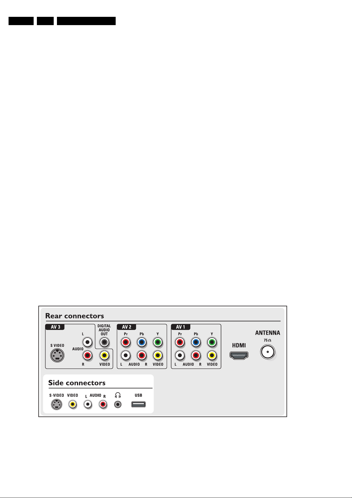
1.2 Connection Overview
Note: The following connector color abbreviations are used
(acc. to DIN/IEC 757): Bk= Black, Bu= Blue, Gn= Green, Gy=
Grey, Rd= Red, Wh= White, and Ye= Yellow.
1.1.2 Sound
Sound systems : AV Stereo
Figure 1-1 I/O connection overview
G_15940_041.eps
240506
Page 3
Technical Specifications, Connections, and Chassis Overview
EN 3EJ2.0U LA 1.
1.2.1 Side Connections
Mini Jack: Audio Headphone - Out
Bk - Headphone 32 - 600 ohm / 10 mW ot
Cinch: Video CVBS - In, Audio - In
Ye - Video CVBS 1 V
Wh - Audio L 0.5 V
Rd - Audio R 0.5 V
/ 75 ohm jq
PP
/ 10 kohm jq
RMS
/ 10 kohm jq
RMS
S-Video (Hosiden): Video Y/C - In
1 -Ground Y Gnd H
2 -Ground C Gnd H
3 -Video Y 1 V
4 -Video C 0.3 V
/ 75 ohm j
PP
P / 75 ohm j
PP
USB1.1
1234
E_06532_022.eps
300904
Figure 1-2 USB (type A)
1-+5V k
2 -Data (-) jk
3 -Data (+) jk
4 -Ground Gnd H
1.2.2 Rear Connections
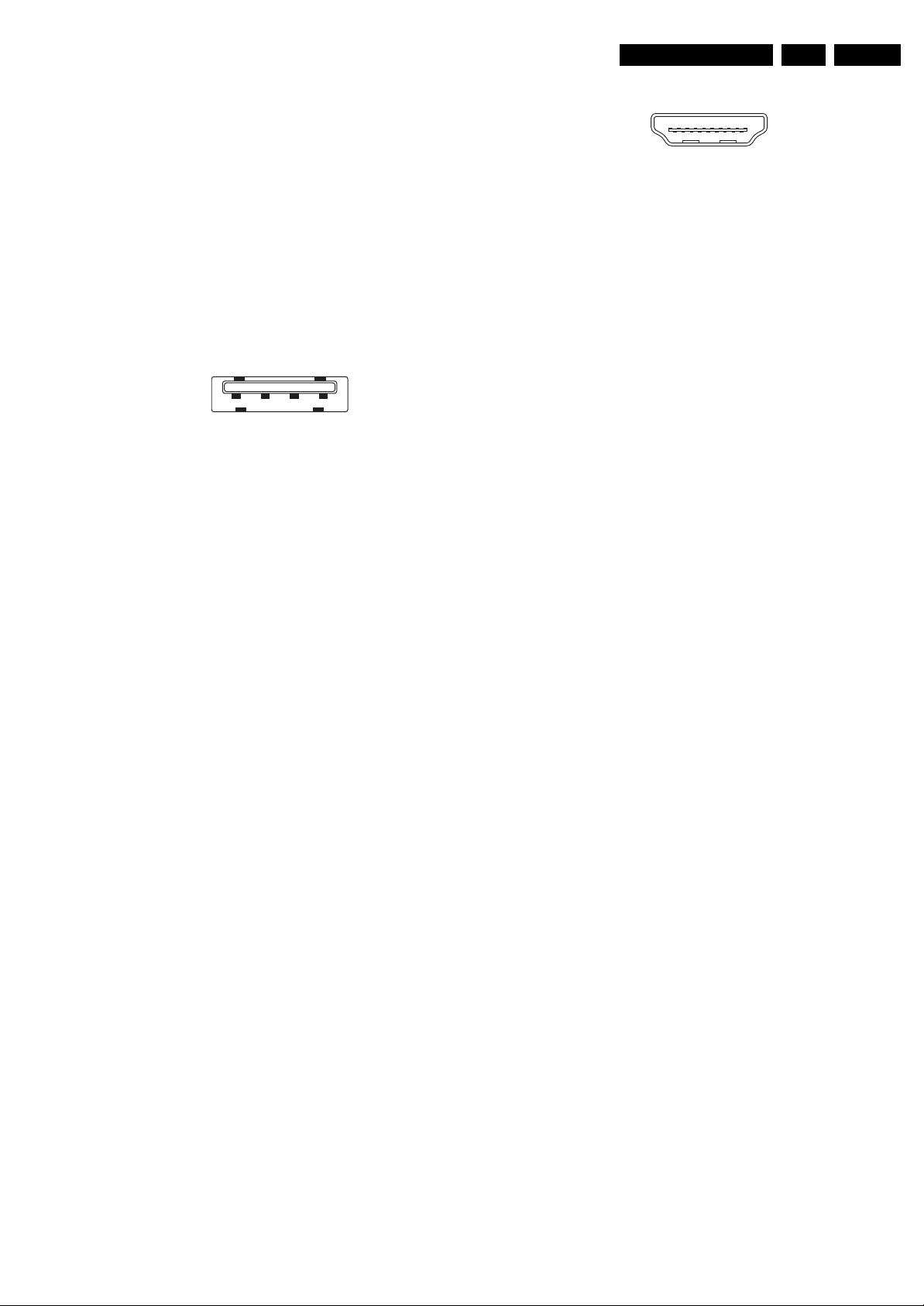
HDMI 1: Digital Video, Digital Audio - In
19
18 2
1
E_06532_017.eps
250505
Figure 1-3 HDMI (type A) connector
1 - D2+ Data channel j
2-Shield Gnd H
3 - D2- Data channel j
4 - D1+ Data channel j
5-Shield Gnd H
6 - D1- Data channel j
7 - D0+ Data channel j
8-Shield Gnd H
9 - D0- Data channel j
10 - CLK+ Data channel j
11 - Shield Gnd H
12 - CLK- Data channel j
13 - n.c.
14 - n.c.
15 - DDC_SCL DDC clock j
16 - DDC_SDA DDC data jk
17 - Ground Gnd H
18 - +5V j
19 - HPD Hot Plug Detect j
20 - Ground Gnd H
Aerial - In
- - F-type (US) Coax, 75 ohm D
AV3 S-Video (Hosiden): Video Y/C - In
1 -Ground Y Gnd H
2 -Ground C Gnd H
3 - Video Y 1 V
4 - Video C 0.3 V
/ 75 ohm j
PP
P / 75 ohm j
PP
AV3 Cinch: Video CVBS - In
Ye - Video CVBS 1 V
/ 75 ohm jq
PP
AV3 Cinch: Audio - In
Wh - Audio L 0.5 V
Rd - Audio R 0.5 V
/ 10 kohm jq
RMS
/ 10 kohm jq
RMS
Cinch: S/PDIF - Out
Bk - Coaxial 0.4 - 0.6V
/ 75 ohm kq
PP
AV2 Cinch: Video YPbPr - In
Gn - Video Y 1 V
Bu - Video Pb 0.7 V
Rd - Video Pr 0.7 V
/ 75 ohm jq
PP
/ 75 ohm jq
PP
/ 75 ohm jq
PP
AV2 Cinch: Video CVBS - In
Ye - Video CVBS 1 V
/ 75 ohm jq
PP
AV2 Cinch: Audio - In
Wh - Audio L 0.5 V
Rd - Audio R 0.5 V
/ 10 kohm jq
RMS
/ 10 kohm jq
RMS
AV1 Cinch: Video YPbPr - In
Gn - Video Y 1 V
PP
Bu - Video Pb 0.7 V
Rd - Video Pr 0.7 V
AV1 Cinch: Video CVBS - In
Ye - Video CVBS 1 V
PP
AV1 Cinch: Audio - In
Wh - Audio L 0.5 V
Rd - Audio R 0.5 V
/ 75 ohm jq
/ 75 ohm jq
PP
/ 75 ohm jq
PP
/ 75 ohm jq
/ 10 kohm jq
RMS
/ 10 kohm jq
RMS
Page 4
EN 4 EJ2.0U LA1.
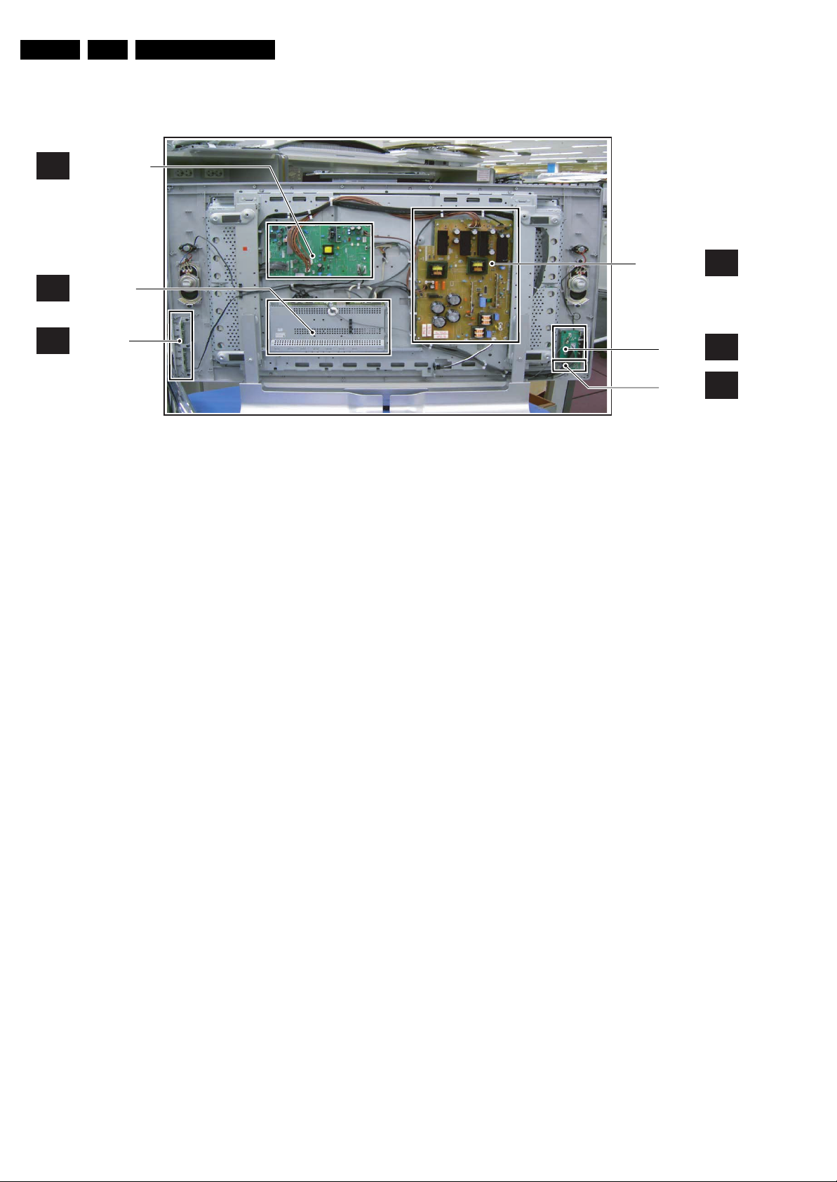
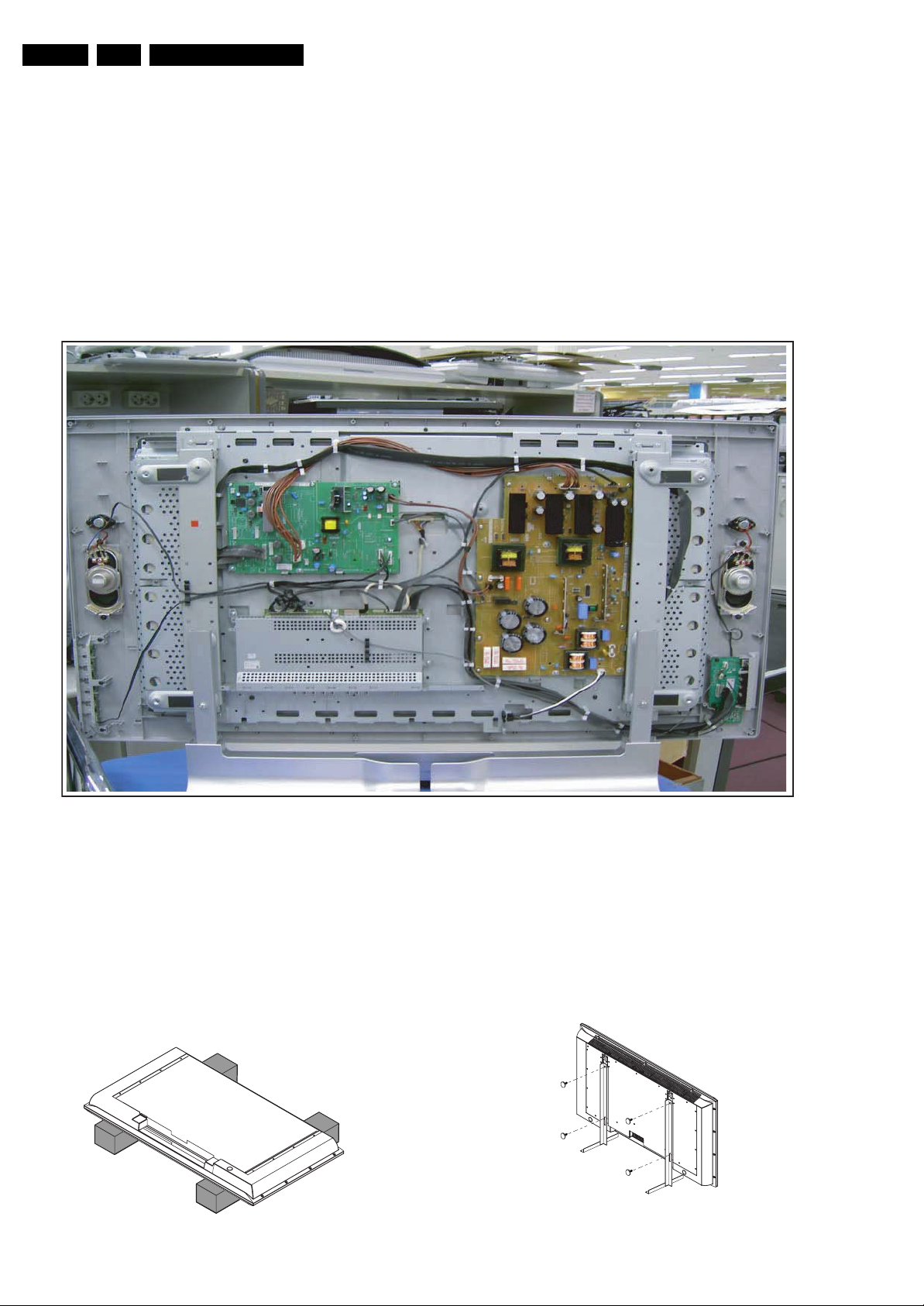
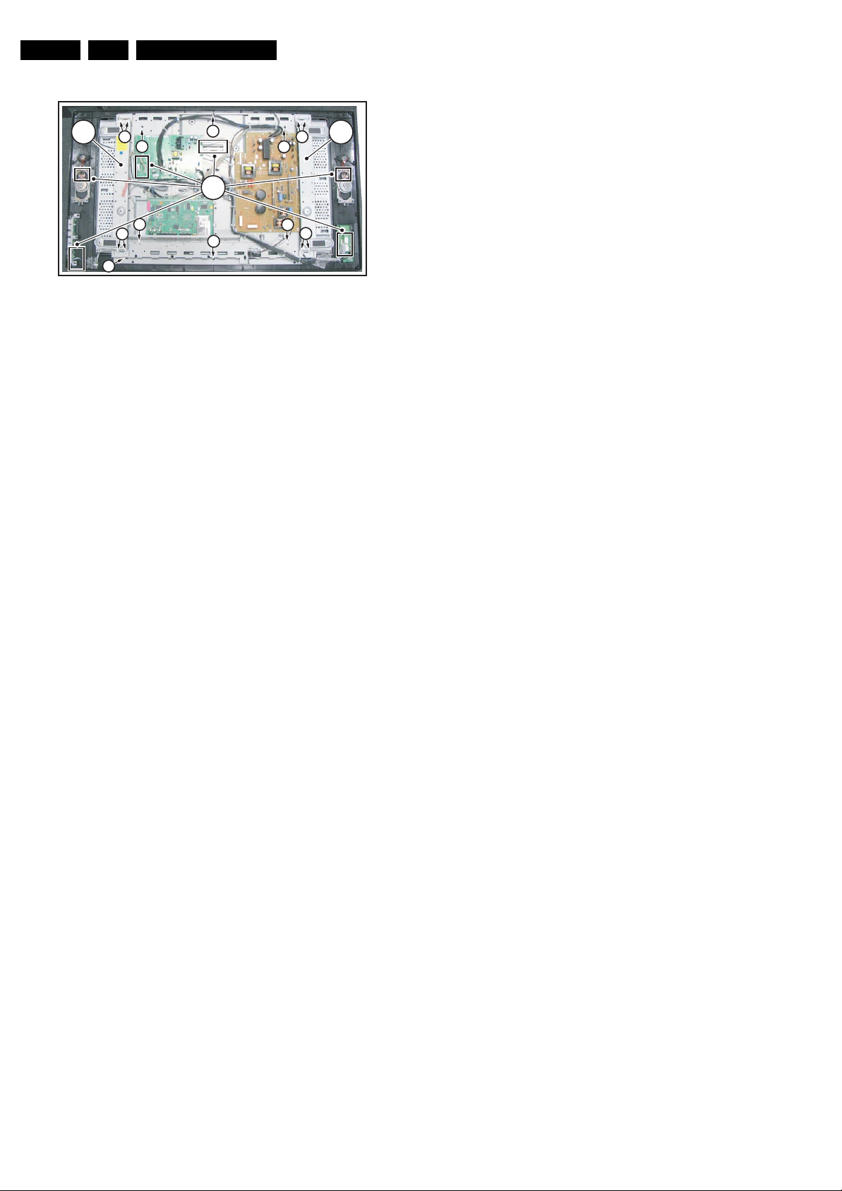
1.3 Chassis Overview
STANDBY &
SA
AUDIO PANEL
Technical Specifications, Connections, and Chassis Overview
SMALL SIGNAL
B
BOARD
CONTROL
E
BOARD
Figure 1-4 PWB/CBA locations
G_15940_042.eps
240506
LCD SUPPLY
PA NE L
SIDE I/O
PA NE L
IR / LED
PA NE L
A
D
J
Page 5

Safety Instructions, Warnings, and Notes
2. Safety Instructions, Warnings, and Notes
EN 5EJ2.0U LA 2.
Index of this chapter:
2.1 Safety Instructions
2.2 Warnings
2.3 Notes
2.1 Safety Instructions
Safety regulations require the following during a repair:
• Connect the set to the Mains/AC Power via an isolation
transformer (> 800 VA).
• Replace safety components, indicated by the symbol h,
only by components identical to the original ones. Any
other component substitution (other than original type) may
increase risk of fire or electrical shock hazard.
Safety regulations require that after a repair, the set must be
returned in its original condition. Pay in particular attention to
the following points:
• Route the wire trees correctly and fix them with the
mounted cable clamps.
• Check the insulation of the Mains/AC Power lead for
external damage.
• Check the strain relief of the Mains/AC Power cord for
proper function.
• Check the electrical DC resistance between the Mains/AC
Power plug and the secondary side (only for sets that have
a Mains/AC Power isolated power supply):
1. Unplug the Mains/AC Power cord and connect a wire
between the two pins of the Mains/AC Power plug.
2. Set the Mains/AC Power switch to the "on" position
(keep the Mains/AC Power cord unplugged!).
3. Measure the resistance value between the pins of the
Mains/AC Power plug and the metal shielding of the
tuner or the aerial connection on the set. The reading
should be between 4.5 Mohm and 12 Mohm.
4. Switch "off" the set, and remove the wire between the
two pins of the Mains/AC Power plug.
• Check the cabinet for defects, to prevent touching of any
inner parts by the customer.
2.2 Warnings
• All ICs and many other semiconductors are susceptible to
electrostatic discharges (ESD w). Careless handling
during repair can reduce life drastically. Make sure that,
during repair, you are connected with the same potential as
the mass of the set by a wristband with resistance. Keep
components and tools also at this same potential. Available
ESD protection equipment:
– Complete kit ESD3 (small tablemat, wristband,
connection box, extension cable and earth cable) 4822
310 10671.
– Wristband tester 4822 344 13999.
• Be careful during measurements in the high voltage
section.
• Never replace modules or other components while the unit
is switched "on".
• When you align the set, use plastic rather than metal tools.
This will prevent any short circuits and the danger of a
circuit becoming unstable.
2.3 Notes
2.3.1 General
• Measure the voltages and waveforms with regard to the
chassis (= tuner) ground (H), or hot ground (I), depending
on the tested area of circuitry. The voltages and waveforms
shown in the diagrams are indicative. Measure them in the
Service Default Mode (see chapter 5) with a color bar
signal and stereo sound (L: 3 kHz, R: 1 kHz unless stated
otherwise) and picture carrier at 475.25 MHz for PAL, or
61.25 MHz for NTSC (channel 3).
• Where necessary, measure the waveforms and voltages
with (D) and without (E) aerial signal. Measure the
voltages in the power supply section both in normal
operation (G) and in stand-by (F). These values are
indicated by means of the appropriate symbols.
• The semiconductors indicated in the circuit diagram and in
the parts lists, are interchangeable per position with the
semiconductors in the unit, irrespective of the type
indication on these semiconductors.
• Manufactured under license from Dolby Laboratories.
“Dolby”, “Pro Logic” and the “double-D symbol”, are
trademarks of Dolby Laboratories.
2.3.2 Schematic Notes
• All resistor values are in ohms, and the value multiplier is
often used to indicate the decimal point location (e.g. 2K2
indicates 2.2 kohm).
• Resistor values with no multiplier may be indicated with
either an "E" or an "R" (e.g. 220E or 220R indicates 220
ohm).
• All capacitor values are given in micro-farads (µ= x10
nano-farads (n= x10
• Capacitor values may also use the value multiplier as the
decimal point indication (e.g. 2p2 indicates 2.2 pF).
• An "asterisk" (*) indicates component usage varies. Refer
to the diversity tables for the correct values.
• The correct component values are listed in the Spare Parts
List. Therefore, always check this list when there is any
doubt.
2.3.3 Rework on BGA (Ball Grid Array) ICs
General
Although (LF)BGA assembly yields are very high, there may
still be a requirement for component rework. By rework, we
mean the process of removing the component from the PWB
and replacing it with a new component. If an (LF)BGA is
removed from a PWB, the solder balls of the component are
deformed drastically so the removed (LF)BGA has to be
discarded.
Device Removal
As is the case with any component that, is being removed, it is
essential when removing an (LF)BGA, that the board, tracks,
solder lands, or surrounding components are not damaged. To
remove an (LF)BGA, the board must be uniformly heated to a
temperature close to the reflow soldering temperature. A
uniform temperature reduces the risk of warping the PWB.
To do this, we recommend that the board is heated until it is
certain that all the joints are molten. Then carefully pull the
component off the board with a vacuum nozzle. For the
appropriate temperature profiles, see the IC data sheet.
Area Preparation
When the component has been removed, the vacant IC area
must be cleaned before replacing the (LF)BGA.
Removing an IC often leaves varying amounts of solder on the
mounting lands. This excessive solder can be removed with
either a solder sucker or solder wick. The remaining flux can be
removed with a brush and cleaning agent.
After the board is properly cleaned and inspected, apply flux on
the solder lands and on the connection balls of the (LF)BGA.
Note: Do not apply solder paste, as this has been shown to
result in problems during re-soldering.
-9
), or pico-farads (p= x10
-12
-6
),
).
Page 6
EN 6 EJ2.0U LA2.
Safety Instructions, Warnings, and Notes
Device Replacement
The last step in the repair process is to solder the new
component on the board. Ideally, the (LF)BGA should be
aligned under a microscope or magnifying glass. If this is not
possible, try to align the (LF)BGA with any board markers.
So as not to damage neighboring components, it may be
necessary to reduce some temperatures and times.
More Information
For more information on how to handle BGA devices, visit this
URL: www.atyourservice.ce.philips.com (needs subscription,
not available for all regions). After login, select “Magazine”,
then go to “Repair downloads”. Here you will find Information
on how to deal with BGA-ICs.
2.3.4 Lead-free Solder
Philips CE is producing lead-free sets (PBF) from 1.1.2005
onwards.
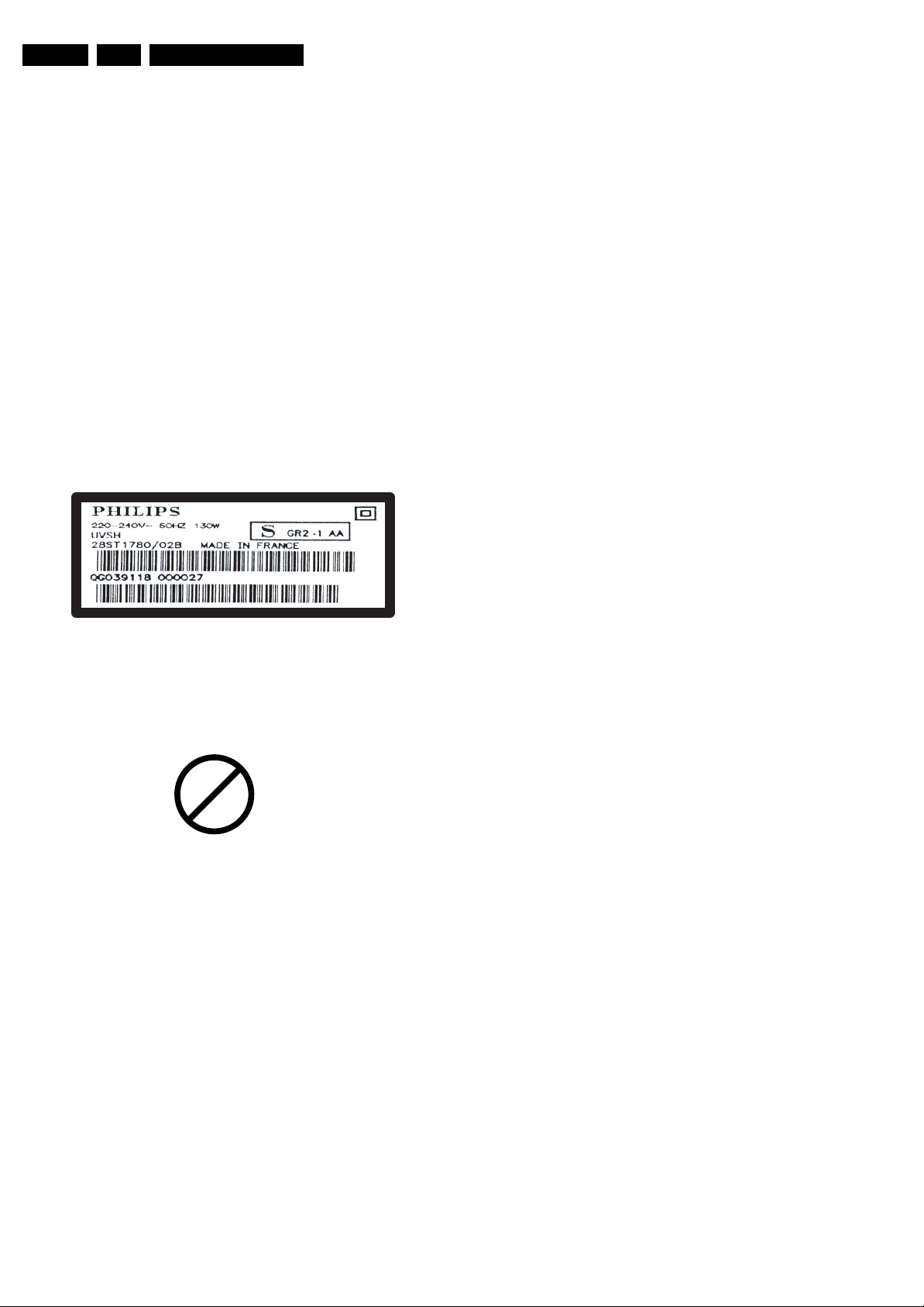
Identification: The bottom line of a type plate gives a 14-digit
serial number. Digits 5 and 6 refer to the production year, digits
7 and 8 refer to production week (in example below it is 1991
week 18).
E_06532_024.eps
230205
avoid mixed regimes. If this cannot be avoided, carefully
clear the solder-joint from old tin and re-solder with new tin.
• Use only original spare-parts listed in the Service-Manuals.
Not listed standard material (commodities) has to be
purchased at external companies.
• Special information for lead-free BGA ICs: these ICs will be
delivered in so-called "dry-packaging" to protect the IC
against moisture. This packaging may only be opened
shortly before it is used (soldered). Otherwise the body of
the IC gets "wet" inside and during the heating time the
structure of the IC will be destroyed due to high (steam-)
pressure inside the body. If the packaging was opened
before usage, the IC has to be heated up for some hours
(around 90°C) for drying (think of ESD-protection!).
Do not re-use BGAs at all!
• For sets produced before 1.1.2005, containing leaded
soldering tin and components, all needed spare parts will
be available till the end of the service period. For the repair
of such sets nothing changes.
In case of doubt whether the board is lead-free or not (or with
mixed technologies), you can use the following method:
• Always use the highest temperature to solder, when using
SAC305 (see also instructions below).
• De-solder thoroughly (clean solder joints to avoid mix of
two alloys).
Caution: For BGA-ICs, you must use the correct temperatureprofile, which is coupled to the 12NC. For an overview of these
profiles, visit the website www.atyourservice.ce.philips.com
(needs subscription, but is not available for all regions)
You will find this and more technical information within the
"Magazine", chapter "Repair downloads".
For additional questions please contact your local repair help
desk.
Figure 2-1 Serial number example
Regardless of the special lead-free logo (which is not always
indicated), one must treat all sets from this date onwards
according to the rules as described below.
P
b
Figure 2-2 Lead-free logo
Due to lead-free technology some rules have to be respected
by the workshop during a repair:
• Use only lead-free soldering tin Philips SAC305 with order
code 0622 149 00106. If lead-free solder paste is required,
please contact the manufacturer of your soldering
equipment. In general, use of solder paste within
workshops should be avoided because paste is not easy to
store and to handle.
• Use only adequate solder tools applicable for lead-free
soldering tin. The solder tool must be able:
– To reach a solder-tip temperature of at least 400°C.
– To stabilise the adjusted temperature at the solder-tip.
– To exchange solder-tips for different applications.
• Adjust your solder tool so that a temperature of around
360°C - 380°C is reached and stabilised at the solder joint.
Heating time of the solder-joint should not exceed ~ 4 sec.
Avoid temperatures above 400°C, otherwise wear-out of
tips will increase drastically and flux-fluid will be destroyed.
To avoid wear-out of tips, switch “off” unused equipment or
reduce heat.
• Mix of lead-free soldering tin/parts with leaded soldering
tin/parts is possible but PHILIPS recommends strongly to
2.3.5 Alternative BOM identification
In September 2003, Philips CE introduced a change in the way
the serial number (or production number, see Figure 2-1) is
composed. From this date on, the third digit in the serial
number (example: AG2B0335000001) indicates the number of
the alternative BOM (Bill of Materials used for producing the
specific model of TV set). It is possible that the same TV model
on the market is produced with e.g. two different types of
displays, coming from two different O.E.M.s.
By looking at the third digit of the serial number, the service
technician can see if there is more than one type of B.O.M.
used in the production of the TV set he is working with. He can
then consult the At Your Service Web site, where he can type
in the Commercial Type Version Number of the TV set (e.g.
28PW9515/12), after which a screen will appear that gives
information about the number of alternative B.O.M.s used.
If the third digit of the serial number contains the number 1
(example: AG1B033500001), then there is only one B.O.M.
version of the TV set on the market. If the third digit is a 2
(example: AG2B0335000001), then there are two different
B.O.M.s. Information about this is important for ordering
the correct spare parts!
For the third digit, the numbers 1...9 and the characters A...Z
can be used, so in total: 9 plus 26 = 35 different B.O.M.s can
be indicated by the third digit of the serial number.
2.3.6 Practical Service Precautions
• It makes sense to avoid exposure to electrical shock.
While some sources are expected to have a possible
dangerous impact, others of quite high potential are of
limited current and are sometimes held in less regard.
• Always respect voltages. While some may not be
dangerous in themselves, they can cause unexpected
reactions that are best avoided. Before reaching into a
powered TV set, it is best to test the high voltage insulation.
It is easy to do, and is a good service precaution.
Page 7

3. Directions for Use
You can download this information from the following websites:
http://www.philips.com/support
http://www.p4c.philips.com
Directions for Use
EN 7EJ2.0U LA 3.
Page 8
EN 8 EJ2.0U LA4.
Mechanical Instructions
4. Mechanical Instructions
Index of this chapter:
4.1 Cable Dressing
4.2 Service Positions
4.3 Assy/Panel Removal
4.4 Set Re-assembly
4.1 Cable Dressing
Notes:
• Several models in this chassis range have a different
mechanical construction, the instructions given in this
chapter are therefore very model specific.
• Figures below can deviate slightly from the actual situation,
due to the different set executions.
• Follow the disassemble instructions in described order.
4.2 Service Positions
For easy servicing of this set, there are a few possibilities
created:
• Foam bars (created for Service).
• Aluminium service stands (created for Service).
4.2.1 Foam Bars
Figure 4-2 Foam bars
E_06532_018.eps
170504
Figure 4-1 Cable dressing
4.2.2 Aluminium Stands
G_16290_091.eps
030206
The foam bars (order code 3122 785 90580 for two pieces) can
be used for all types and sizes of Flat TVs. By laying the TV
face down on the (ESD protective) foam bars, a stable situation
is created to perform measurements and alignments.
By placing a mirror under the TV, you can monitor the screen.
E_06532_019.eps
170504
Figure 4-3 Aluminium stands (drawing of MkI)
Page 9
The new MkII aluminium stands (not on drawing) with order
code 3122 785 90690, can also be used to do measurements,
alignments, and duration tests. The stands can be
(dis)mounted quick and easy by means of sliding them in/out
the "mushrooms". The new stands are backwards compatible
with the earlier models.
Important: For (older) FTV sets without these "mushrooms", it
is obligatory to use the provided screws, otherwise it is possible
to damage the monitor inside!.
4.3 Assy/Panel Removal
4.3.1 Rear Cover
2
1
Figure 4-4 Rear cover lid removal
Mechanical Instructions
G_15940_047.eps
240506
EN 9EJ2.0U LA 4.
5
5
5
5
2
5
1
1
5
5
5
5
5
5
5
5
Figure 4-6 Rear cover removal
Warning: Disconnect the mains power cord before you remove
the rear cover.
1. Place the TV set upside down on a table top, using the
foam bars (see part "Foam Bars").
Caution: do not put pressure on the display, but let the
monitor lean on the speakers or the Front cover.
2. Remove the screws [1] that hold the rear cover lids and
remove the lids [2]. See figure “Rear cover lid removal” for
details.
3. Disconnect the connectors [3] behind the lids. See figure
“AmbiLight connector removal” for details.
4. Remove the mushrooms [4]. See figure “Rear cover
removal” for details.
5. Remove screws [5].
6. Lift the rear cover from the cabinet cautiously. Make sure
that wires and other internal components are not damaged
during cover removal.
55
5
5
5
5
14
5
5
5
5
5
G_15940_049.eps
5
5
240506
5
3
Figure 4-5 AmbiLight connector removal
G_15940_048.eps
240506
4.3.2 Keyboard Control Panel
1. Remove the screws [1] that secure the panel. See figure
“Keyboard Control panel” for details.
2. Slide the bracket to the right.
3. Release clips [2].
4. Remove the panel.
5. Unplug connector [3].
When defective, replace the whole unit.
1
Figure 4-7 Keyboard Control panel (1)
G_15940_050.eps
240506
Page 10
EN 10 EJ2.0U LA4.
s
6
Mechanical Instructions
Caution: never disconnect the speakers with a playing set,
because otherwise the class-D audio amplifiers could be
damaged!
4.3.6 Stand-by Power Supply/Audio Amplifier Panel
1. Disconnect all connectors [1] from the panel.
2. Remove the fixation screws [2] from the panel.
2
3. Take the panel out of its brackets (it hinges at the right
side).
2
3
Figure 4-8 Keyboard Control panel (2)
4.3.3 Side I/O Panel
6. Unplug connectors [1].
7. Remove screws [2]. See figure “Side I/O and LED Panel
removal” for details.
When defective, replace the whole unit.
2
1
G_15940_051.eps
240506
2
1
2
2
Figure 4-10 Stand-by/Audio panel
4.3.7 LCD Supply Panel
1. Disconnect all cables [1] from the panel.
2. Remove the fixation screws [2] from the panel.
3. Take the panel out of its brackets (it hinges on the right
side).
1
G_15940_053.eps
260506
4
Figure 4-9 Side I/O and LED Panel removal
4.3.4 LED Panel
1. Release clip [3].
2. Remove the panel.
3. Unplug connector [4].
When defective, replace the whole unit.
4.3.5 Speakers
After removal of the rear cover, you can access the speakers.
3
G_15940_052.eps
240506
1
2
1
1
Figure 4-11 LCD supply panel
G_15940_054.ep
26050
Page 11
4.3.8 Small Signal Board (SSB)
s
6
REAR COVER
LEFT
RIGHT
1
1 1 1
Mechanical Instructions
EN 11EJ2.0U LA 4.
1
1
1
G_16290_072.eps
310106
Figure 4-12 SSB bottom shielding
1. Remove the connector fixation screws [1] at the connector
plate (bottom side, see Figure “SSB bottom shielding”).
2. Unplug the LVDS connector [1] on the SSB (SSB top side,
see Figure “SSB top view”). Be careful as it is very fragile.
3. Unplug all other cables on the SSB.
4. Remove the mounting screws [2] that hold the SSB, and lift
the panel from the set.
1
2
2
G_15940_057.eps
Figure 4-15 Left AmbiLight panel removal
1. Unplug connectors [1].
2. Remove screws [2].
3. Remove panel.
Right AmbiLight Panel Removal
See figure “Right AmbiLight panel removal” for details.
2
260506
4.3.9 AmbiLight Inverter Panel
The AmbiLight inverter panels are placed on the inside of the
rear cover. See figure “AmbiLight inverter panels” for details.
LEFT
Figure 4-14 AmbiLight inverter panels
Left AmbiLight Panel Removal
See figure “Left AmbiLight panel removal” for details.
Figure 4-13 SSB top view
REAR COVER
G_15940_055.ep
24050
RIGHT
G_15940_056.eps
240506
2
Figure 4-16 Right AmbiLight panel removal
1. Unplug connectors [1].
2. Remove screws [2].
3. Remove panel.
4.3.10 LCD Panel
See figure “LCD panel removal” for details.
1
2
G_15940_058.eps
260506
Page 12
EN 12 EJ2.0U LA4.
Mechanical Instructions
1
4
4
1
1
Figure 4-17 LCD panel removal
To remove the LCD-panel, carry out the following steps:
1. Remove screws [1].
2. Remove brackets [2].
3. Important: Unplug the LVDS connector [3] on the LCD
panel. Be careful, as this is a very fragile connector!
4. Unplug all other connectors [3].
5. Remove screws [4].
6. Lift the metal frame (together with all PWBs) from the set.
Take care not to damage the fragile LVDS cable.
7. After removal of the metal frame, you can lift the LCD panel
from the front cabinet.
1
3
1
4.4 Set Re-assembly
1
4
4
1
G_15940_059.eps
22
260506
To re-assemble the whole set, execute all processes in reverse
order.
Notes:
• While re-assembling, make sure that all cables are placed
and connected in their original position. See Figure "Cable
dressing".
• Ensure that the conducting tape [1] at both sides of the
LCD panel is placed in its original position. See Figure
“Conducting tape”.
Page 13
Service Modes, Error Codes, and Fault Finding
5. Service Modes, Error Codes, and Fault Finding
EN 13EJ2.0U LA 5.
Index of this chapter:
5.1 Test Points
5.2 Service Modes
5.3 Stepwise Start-up
5.4 Service Tools
5.5 Error Codes
5.6 The Blinking LED Procedure
5.7 Protections
5.8 Fault Finding and Repair Tips
5.9 Software Upgrading
5.1 Test Points
As most signals are digital, it will be almost impossible to
measure waveforms with a standard oscilloscope. Therefore,
waveforms are not given in this manual. Several key ICs are
capable of generating test patterns, which can be controlled via
ComPair. In this way it is possible to determine which part is
defective.
Perform measurements under the following conditions:
• Service Default Mode.
• Video: Color bar signal.
• Audio: 3 kHz left, 1 kHz right.
5.2 Service Modes
Service Default Mode (SDM) and Service Alignment Mode
(SAM) offer several features for the service technician, while
the Customer Service Mode (CSM) is used for communication
between a Customer Helpdesk and a customer.
There is also the option of using ComPair, a hardware interface
between a computer (see requirements below) and the TV
chassis. It offers the ability of structured troubleshooting, test
pattern generation, error code reading, software version
readout, and software upgrading.
Minimum requirements for ComPair: a Pentium processor,
Windows 95/98, and a CD-ROM drive (see also paragraph
“ComPair”).
in the channel map and could be different from the one
corresponding to the physical channel 3.
• All picture settings at 50% (brightness, color, contrast).
• All sound settings at 50%, except volume at 25%.
• All service-unfriendly modes (if present) are disabled, like:
– (Sleep) timer.
– Child/parental lock.
– Picture mute (blue mute or black mute).
– Automatic volume levelling (AVL).
– Auto switch "off" (when no video signal was received
for 10 minutes).
– Skip/blank of non-favorite pre-sets.
– Smart modes.
– Auto store of personal presets.
– Auto user menu time-out.
How to Activate SDM
Use one of the following methods:
• Use the standard RC-transmitter and key in the code
“062596”, directly followed by the “MENU” button.
Note: It is possible that, together with the SDM, the main
menu will appear. To switch it "off", push the “MENU”
button again.
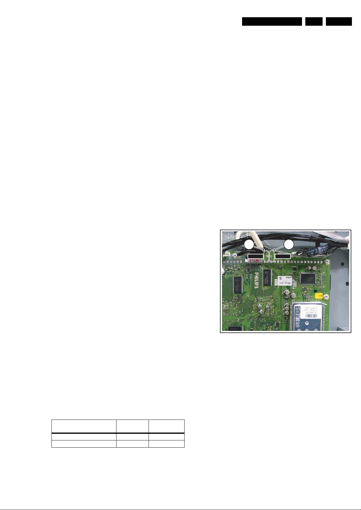
• Short for a moment the two solder pads [1] on the SSB,
with the indication “SDM”. They are located outside the
shielding. Activation can be performed in all modes, except
when the set has a problem with the Stand-by Processor.
See figure “SDM and SPI service pads”.
12
SDMSPI
5.2.1 Service Default Mode (SDM)
Purpose
• To create a pre-defined setting, to get the same
measurement results as given in this manual.
• To override SW protections (only applicable for protections
detected by stand-by processor) and make the TV start up
to the step just before protection (a sort of automatic
stepwise start up). See paragraph “Stepwise Start Up”.
• To start the blinking LED procedure (not valid in protection
mode).
Specifications
Table 5-1 SDM default settings
Region Freq. (MHz)
Europe, AP-PAL/Multi 475.25 PAL B/G
NAFTA, AP-NTSC, LATAM 61.25 (ch. 3) NTSC M
• Tuning frequency 61.25 MHz for NTSC: The TV shall tune
to physical channel 3 only if channel 3 is an analog channel
or if there is no channel 3 installed in the channel map. If
there is a digital channel installed in channel 3, then the
frequency to which the set will tune, would be as specified
Default
system
Figure 5-1 SDM and SDI service pads
After activating this mode, “SDM” will appear in the upper right
corner of the screen (if you have picture).
How to Navigate
When you press the “MENU” button on the RC transmitter, the
set will toggle between the SDM and the normal user menu
(with the SDM mode still active in the background).
How to Exit SDM
Use one of the following methods:
• Switch the set to STAND-BY via the RC-transmitter.
• Via a standard customer RC-transmitter: key in “00”sequence.
5.2.2 Service Alignment Mode (SAM)
Purpose
• To perform (software) alignments.
• To change option settings.
• To easily identify the used software version.
G_16300_001.eps
020206
Page 14
EN 14 EJ2.0U LA5.
Service Modes, Error Codes, and Fault Finding
• To view operation hours.
• To display (or clear) the error code buffer.
How to Activate SAM
Via a standard RC transmitter: key in the code “062596”
directly followed by the “INFO” button. After activating SAM
with this method a service warning will appear on the screen,
you can continue by pressing the red button on the RC.
Contents of SAM:
• Hardware Info.
– A. VIPER SW Version. Displays the software version
of the VIPER software (main software) (example:
EJ20U-1.2.3.4_12345 = AAAAB_X.Y.W.Z_NNNNN).
• AAAA= the chassis name.
• B= the region: A= AP, E= EU, L= Latam, U = US.
• X.Y.W.Z= the software version, where X is the
main version number (different numbers are not
compatible with one another) and Y.W.Z is the sub
version number (a higher number is always
compatible with a lower number).
• NNNNN= last five digits of 12nc code of the
software.
– B. SBY PROC Version. Displays the software version
of the stand-by processor.
– C. Production Code. Displays the production code of
the TV, this is the serial number as printed on the back
of the TV set. Note that if an NVM is replaced or is
initialized after corruption, this production code has to
be re-written to NVM. ComPair will foresee in a
possibility to do this.
• Operation Hours. Displays the accumulated total of
operation hours (not the stand-by hours). Every time the
TV is switched "on/off", 0.5 hours is added to this number.
• Errors. (Followed by maximal 10 errors). The most recent
error is displayed at the upper left (for an error explanation
see paragraph “Error Codes”).
• Defective Module. Here the module that generates the
error is displayed. If there are multiple errors in the buffer,
which are not all generated by a single module, there is
probably another defect. It will then display the message
“UNKNOWN” here.
• Reset Error Buffer. When you press “cursor right” and
then the “OK” button, the error buffer is reset.
• Alignments. This will activate the “ALIGNMENTS” submenu. See also paragraph 8.
• Dealer Options. Extra features for the dealers.
• Options. Extra features for Service. See also paragraph 8.
• Initialize NVM. When an NVM was corrupted (or replaced)
in the former EMG based chassis, the microprocessor
replaces the content with default data (to assure that the
set can operate). However, all preferences and alignment
values are gone now, and option numbers are not correct.
Therefore, this was a very drastic way. In this chassis, the
procedure is implemented in another way: The moment the
processor recognizes a corrupted NVM, the “initialize
NVM” line will be highlighted. Now, you can do two things
(dependent of the service instructions at that moment):
– Save the content of the NVM via ComPair for
development analysis, before initializing. This will give
the Service department an extra possibility for
diagnosis (e.g. when Development asks for this).
– Initialize the NVM (same as in the past, however now it
happens conscious).
Note: When you have a corrupted NVM, or you have replaced
the NVM, there is a high possibility that you will not have picture
any more because your display option is not correct. So, before
you can initialize your NVM via the SAM, you need to have a
picture and therefore you need the correct display option. To
adapt this option, use ComPair. The correct HEX values for the
options can be found in the table below.
Changing the display option code via a standard RC:
Key in the code “062598” directly followed by the “MENU”
button and “XXX” (where XXX is the 3 digit decimal display
option code as mentioned in the first column of the next table).
Make sure to key in all three digits, also the leading zero’s. If
the above action is successful, the front LED will go out as an
indication that the RC sequence was accepted.
After the display option is changed in the NVM, the TV will go
to the Stand-by mode.
If the NVM was corrupted or empty before this action, it will be
initialized first (loaded with the default values). This initializing
can take up to 20 seconds.
When you have keyed in the wrong display option code, it is
possible that the TV will not start up properly. In some cases
the TV will go to standby again. In this case you need to reprogram the NVM via ComPair.
Table 5-2 Display option code overview (all FTV chassis)
Display Op-
tion (Dec.)
000 PDP SDI V3 42” 768p 1024
001 PDP SDI V3 50” 768p 1366
002 PDP FHP A1 42” 1024i 1024
003 LCD LPL A3 30” 768p 1280
004 LCD LPL A6 37” 768p 1366
005 LCD LPL A6 42” 768p 1366
006 LCD Sharp 32” 768p 1366
007 PDP SDI V3 42” 480p 852
008 PDP FHP A1 37” 1024i 1024
009 LCOS XION - - 720p 1280
010 LCD AUO 30” 768p 1280
011 LCD LPL A6 32” 768p 1366
012 LCD AUO V0.1 32” 768p 1366
013 LCD Sharp 37” 768p 1366
014 LCD LPL SL01 42” 1080p 1920
015 PDP SDI 37” 480p 852
016 PDP FHP 37” 1080i 1024
017 PDP FHP 42” 1080i 1024
018 PDP FHP 55” 768p 1366
019 LCOS VENUS - - 720p 1280
020 LCOS VENUS - - 1080p 1920
021 LCD LPL SL01 26” 768p 1366
022 LCD LPL SL01 32” 768p 1366
023 PDP LG 42” 480p 852
024 PDP SDI V4 42” 480p 852
025 PDP SDI V5 42” 768p 1024
026 PDP FHP A2 42” 1024i 1024
027 PDP SDI V5 50” 768p 1366
028 LCD Sharp 37” 1080p 1920
029 LCD AUO V0.1 32” 768p 1366
030 LCD Sharp 37” 1080p 1920
031 LCD Sharp 37” 1080p 1920
032 LCD LPL SL0.1 20” 768p 1366
033 LCD QDI 23” 768p 1366
034 ECO PTV - 52” 1080i 1366
035 ECO PTV - 55” 1080i 1366
036 ECO PTV - 61” 1080i 1366
037 PDP FHP A3 42” 1024i 1024
038 DLP - 50” 720p 1280
039 DLP - 60” 720p 1280
040 LCD Sharp 2.3 32” 768p 1366
041 LCD LPL SLA1 42” 768p 1366
042 PDP SDI V4 63” 768p 1366
043 LCD Sharp 3.0 37” 768p 1366
044 LCD Sharp 2.3 37” 768p 1366
045 LCD LPL SLB2 26” 768p 1366
046 LCD LPL SL06 32” 768p 1366
Technology Display
Make &
Type
Size Vertical
Resolution
Horizontal
Resolution
Page 15

Service Modes, Error Codes, and Fault Finding
EN 15EJ2.0U LA 5.
Display Op-
tion (Dec.)
047 LCD LPL SLB1 42” 768p 1366
048 LCD QDI 26” 768p 1366
049 LCD AUO 26” 768p 1366
050 LCD AUO V9 32” 768p 1366
051 LCD AUO 37” 768p 1366
052 LCD AUO V5 32” 768p 1366
053 LCD LPL SL04 37” 768p 1366
Technology Display
Make &
Type
Size Vertical
Resolution
• Store. All options and alignments are stored when
pressing “cursor right” and then the “OK”-button
• SW Maintenance.
– SW Events. Not useful for service purposes. In case of
specific software problems, the development
department can ask for this info.
– HW Events. Not useful for service purposes. In case of
specific software problems, the development
department can ask for this info.
• Operation hours PDP. Displays the accumulated total of
PDP operation hours. For the LCD chassis this is not
applicable. Here you are able to reset the operation hours
of the plasma display. This has to be done in case of
replacement of the display.
How to Navigate
• In SAM, you can select the menu items with the “CURSOR
UP/DOWN” key on the RC-transmitter. The selected item
will be highlighted. When not all menu items fit on the
screen, move the “CURSOR UP/DOWN” key to display the
next/previous menu items.
• With the “CURSOR LEFT/RIGHT” keys, it is possible to:
– (De) activate the selected menu item.
– (De) activate the selected submenu.
How to Exit SAM
Use one of the following methods:
• Press the “MENU” button on the RC-transmitter.
• Switch the set to STAND-BY via the RC-transmitter.
Note: As long as SAM is activated, it is not possible to change
a channel. This could hamper the White Point alignments
because you cannot choose your channel/frequency any more.
Workaround: after you have sent the RC code “062596 INFO”
you will see the service-warning screen, and in this stage it is
still possible to change the channel (so before pressing the
“OK” button).
5.2.3 Customer Service Mode (CSM)
Purpose
When a customer is having problems with his TV-set, he can
call his dealer or the Customer Helpdesk. The service
technician can then ask the customer to activate the CSM, in
order to identify the status of the set. Now, the service
technician can judge the severity of the complaint. In many
cases, he can advise the customer how to solve the problem,
or he can decide if it is necessary to visit the customer.
The CSM is a read only mode; therefore, modifications in this
mode are not possible.
How to Activate CSM
Key in the code “123654” via the standard RC transmitter.
Note: Activation of the CSM is only possible if there is no (user)
menu on the screen!
How to Navigate
By means of the “CURSOR-DOWN/UP” knob on the RCtransmitter, you can navigate through the menus.
Horizontal
Resolution
Contents of CSM
• SW Version (example: EJ20U-1.2.3.4_12345). Displays
the built-in main software version. In case of field problems
related to software, software can be upgraded. As this
software is consumer upgradeable, it will also be published
on the Internet.
• SBY Processor Version. Displays the built-in stand-by
processor software version. Upgrading this software will be
possible via a PC and a ComPair interface (see chapter
Software upgrade).
• Set Type. This information is very helpful for a helpdesk/
workshop as reference for further diagnosis. In this way, it
is not necessary for the customer to look at the rear of the
TV-set. Note that if an NVM is replaced or is initialized after
corruption, this set type has to be re-written to NVM.
ComPair will foresee a possibility to do this.
• Production Code. Displays the production code (the serial
number) of the TV. Note that if an NVM is replaced or is
initialized after corruption, this production code has to be
re-written to NVM. ComPair will foresee a possibility to do
this.
• Code 1. Gives the latest five errors of the error buffer. As
soon as the built-in diagnose software has detected an
error the buffer is adapted. The last occurred error is
displayed on the leftmost position. Each error code is
displayed as a 2-digit number. When less than 10 errors
occur, the rest of the buffer is empty (00). See also
paragraph Error Codes for a description.
• Code 2. Gives the first five errors of the error buffer. See
also paragraph Error Codes for a description.
• Headphone Volume. Gives the last status of the
headphone volume, as set by the customer. The value can
vary from 0 (volume is minimum) to 100 (volume is
maximum). Change via”MENU”, “TV”, “SOUND”,
“HEADPHONE VOLUME”.
• Dolby. Indicates whether the received transmitter
transmits Dolby sound (“ON”) or not (“OFF”). Attention: The
presence of Dolby can only be tested by the software on
the Dolby Signaling bit. If a Dolby transmission is received
without a Dolby Signaling bit, this indicator will show “OFF”
even though a Dolby transmission is received.
• Sound Mode. Indicates the by the customer selected
sound mode (or automatically chosen mode). Possible
values are “STEREO” and “VIRTUAL DOLBY
SURROUND”. Change via “MENU”, “TV”, “SOUND”,
“SOUND MODE”. It can also have been selected
automatically by signaling bits (internal software).
• Digital Processing. Indicates the selected digital mode.
Possible values are “STANDARD” and “PIXEL PLUS”.
Change via “MENU”, “TV”, “PICTURE”, “DIGITAL
PROCESSING”.
• TV System. Gives information about the video system of
the selected transmitter.
– M: NTSC M signal received
– ATSC: ATSC signal received
• Center Mode. Not applicable.
• DNR. Gives the selected DNR setting (Dynamic Noise
Reduction), “OFF”, “MINIMUM”, “MEDIUM”, or
“MAXIMUM”. Change via “MENU”, “TV”, “PICTURE”,
“DNR”
• Noise Figure. Gives the noise ratio for the selected
transmitter. This value can vary from 0 (good signal) to 127
(average signal) and to 255 (bad signal). For some
software versions, the noise figure will only be valid when
“Active Control” is set to “medium” or “maximum” before
activating CSM. The noise figure is not applicable for digital
channels.
• Source. Indicates which source is used and the video/
audio signal quality of the selected source. (Example:
Tuner, Video/NICAM) Source: “TUNER”, “AV1”, “AV2”,
“AV3”, “HDMI 1”, “SIDE”. Video signal quality: “VIDEO”, “SVIDEO”, “RGB 1FH”, “YPBPR 1FH 480P”, “YPBPR 1FH
576P”, “YPBPR 1FH 1080I”, “YPBPR 2FH 480P”, “YPBPR
2FH 576P”, “YPBPR 2FH 1080I”, “RGB 2FH 480P”, “RGB
Page 16
EN 16 EJ2.0U LA5.
Service Modes, Error Codes, and Fault Finding
2FH 576P” or “RGB 2FH 1080I”. Audio signal quality:
“STEREO”, “SPDIF 1”, “SPDIF 2”, or “SPDIF”.
• Audio System. Gives information about the audible audio
system. Possible values are “Stereo”, ”Mono”, “Mono
selected”, “Analog In: No Dig. Audio”, “Dolby Digital 1+1”,
“Dolby Digital 1/0”, “Dolby Digital 2/0”, “Dolby Digital 2/1”,
“Dolby Digital 2/2”, “Dolby Digital 3/0”, “Dolby Digital 3/1”,
“Dolby Digital 3/2”, “Dolby Digital Dual I”, “Dolby Digital
Dual II”, “MPEG 1+1”, “MPEG 1/0”, “MPEG 2/0”. This is the
same info as you will see when pressing the “INFO” button
in normal user mode (item “signal”). In case of ATSC
receiving there will be no info displayed.
• Tuned Bit. Due to the ATSC architectural setup, this item
does not give useful information anymore.
• Preset Lock. Indicates if the selected preset has a child
lock: “LOCKED” or “UNLOCKED”. Change via “MENU”,
“TV”, “CHANNELS”, “CHANNEL LOCK”.
• Lock After. Indicates at what time the channel lock is set:
“OFF” or e.g. “18:45” (lock time). Change “MENU”, “TV”,
“CHANNELS”, “LOCK AFTER”.
• TV Ratings Lock. Indicates the “TV ratings lock” as set by
the customer. Change via “MENU”, “TV”, “CHANNELS”,
“TV RATINGS LOCK”. Possible values are: “ALL”,
“NONE”, “TV-Y”, “TV-Y7”, “TV-G”, “TV-PG”, “TV-14” and
“TV-MA”.
• Movie Ratings Lock. Indicates the “Movie ratings lock” as
set by the customer. Change via “MENU”, “TV”,
“CHANNELS”, “MOVIE RATINGS LOCK”. Possible values
are: “ALL”, “NR”, “G”, “PG”, “PG-13”, “R”, “NC-17” and “X”.
• V-Chip TV Status. Indicates the setting of the V-chip as
applied by the selected TV channel. Same values can be
shown as for “TV RATINGS LOCK”.
• V-Chip Movie Status. Indicates the setting of the V-chip
as applied by the selected TV channel. Same values can
be shown as for “MOVIE RATINGS LOCK”.
• Options 1. Gives the option codes of option group 1 as set
in SAM (Service Alignment Mode).
• Options 2. Gives the option codes of option group 2 as set
in SAM (Service Alignment Mode).
• AVL. Indicates the last status of AVL (Automatic Volume
Level): “ON” or “OFF”. Change via “MENU”, “TV”,
“SOUND”, “AVL”. AVL can not be set in case of digital
audio reception (e.g. Dolby Digital or AC3)
• Delta Volume. Indicates the last status of the delta volume
for the selected preset as set by the customer: from “-12”
to “+12”. Change via “MENU”, “TV”, “SOUND”, “DELTA
VOLUME”.
• HDMI key validity. Indicates if the HDMI keys (or HDCP
keys) are valid or not. In case these keys are not valid and
the customer wants to make use of the HDMI functionality,
the SSB has to be replaced.
• IEEE key validity. Not applicable.
• POD key validity. Not applicable.
• Digital Signal Quality. This item does not work correct, so
it gives no useful information.
How to Exit CSM
Press any key on the RC-transmitter (with exception of the
“CHANNEL +/-”, “VOLUME”, “MUTE” and digit (0-9) keys).
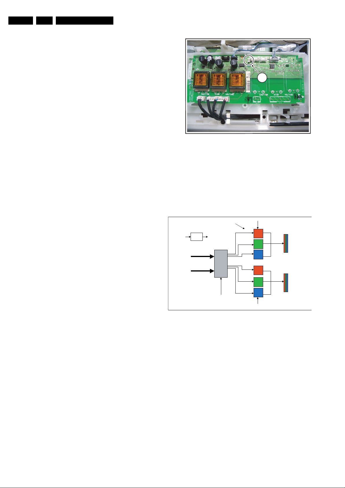
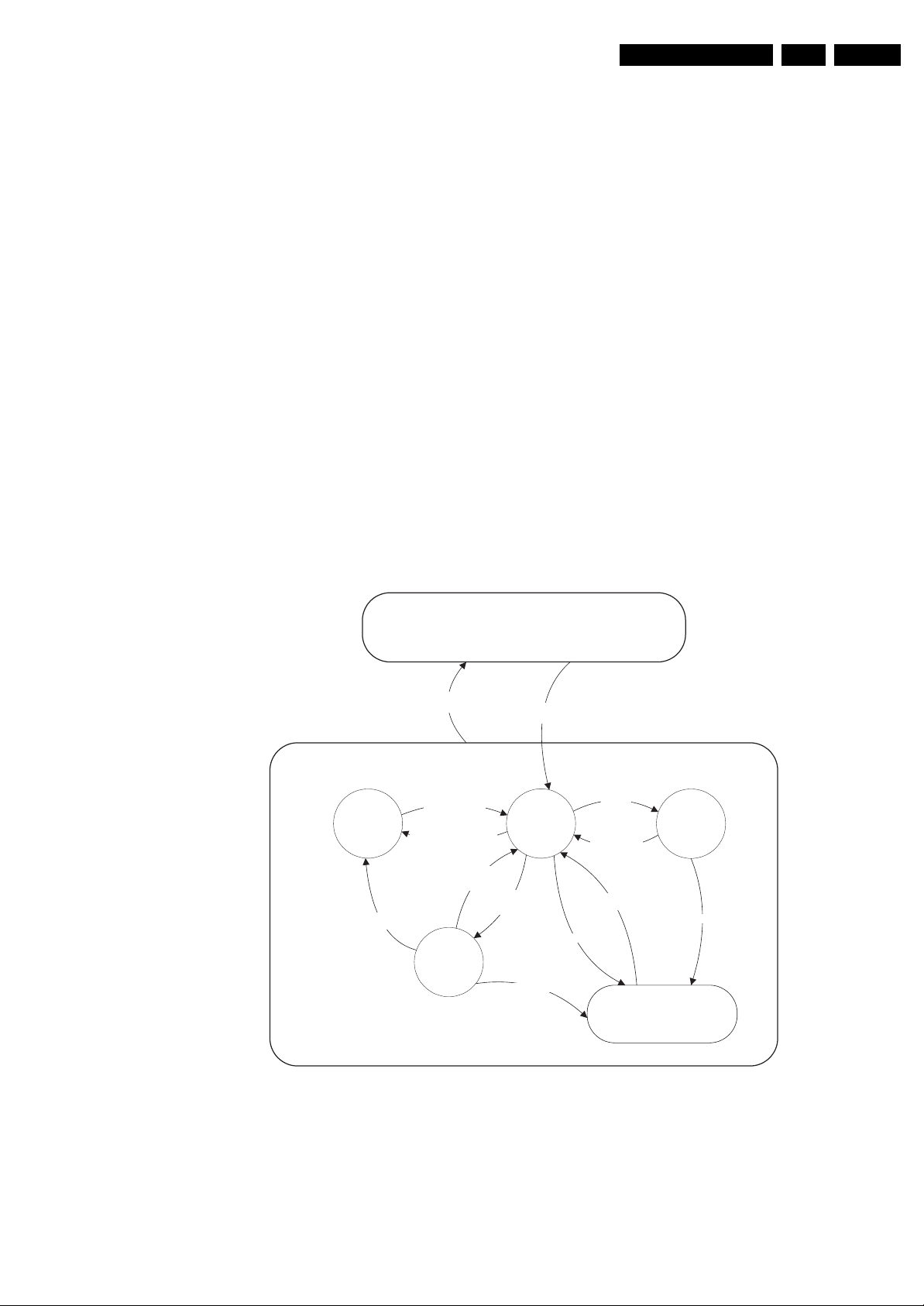
5.2.4 Service Mode of Converter Boards for Ambi Light
Purpose
To switch on the lamps manually in case I
2
C-bus triggering
fails.
The Service Mode can be activated by disconnecting
connector 1M49 and then by shorting for a moment the two
solder pads [1] on the Ambi Light Inverter Panel. See figure
“Service Mode pads”.
1
G_15950_049.eps
Figure 5-2 Service Mode pads AmbiLight panel
In this chassis, single fitted boards are used. It drives 1 lamp
unit (3 lamps) per board.
The double fitted boards (which are used in other sets) are
supplied by +12Va and +12Vb. The microprocessor is supplied
by +12Va.
Therefore, if only +12Va is available, lamp unit B will not work.
See figure “Building blocks of Converter Board” for details.
+12Va
Stab.
Board select
+5V
Inverters
µ
Processor
PWM out
+12Va
I²C
Protection
+12Vb (12
Figure 5-3 Building blocks of Converter Board
The microprocessor performs the following tasks:
• Dimming of Ambi Light by means of PWM.
• Translation of I
2
C-bus commands to PWM.
• Switches the Ambi Light board to protection if needed (in
case of protection only the lamps switch off, no set
protection is triggered).
There are two ways of protection: parallel arcing protection and
serial arcing protection.
Parallel arcing protection is performed by sensing the switching
frequency. In case of short circuit of the transformer output, this
frequency > 100 kHz and the board goes into protection.
Serial arcing protection is performed by detection of arc in
ground wire of the lamp units. In this case, the protection pulse
is transmitted via an opto-coupler.
Protection can be disabled by short-circuiting diode 6112 or
capacitor 2173 or by connecting pin 8 of the microprocessor to
ground.
Repair Tips
In case only one or no lamp unit at all works, probably the
+12Vb (12 - 13 V) is not available or the fuse is broken. Check
for broken MOSFETS or check if they are switched off properly
-13V)
060406
Lamp unit A
Lamp unit B
G_15950_050.eps
060406
Page 17
Service Modes, Error Codes, and Fault Finding
EN 17EJ2.0U LA 5.
by the transistors connected to the PWM outputs of the
microprocessor.
In case the Ambi Light switches off after two seconds, serial
arcing or parallel arcing protection is active. Serial arcing
protection can be excluded by disconnecting the opto-coupler;
check for bad solder joints on transformer or lamp units.
Parallel arcing protection can be disabled by grounding pin 8 of
the microprocessor. Usually the switching frequency (normally
63 kHz) will then be too high. Possible causes are one
MOSFET of the converter has no gate drive or is broken, or
there is a short-circuit of the output of the transformer.
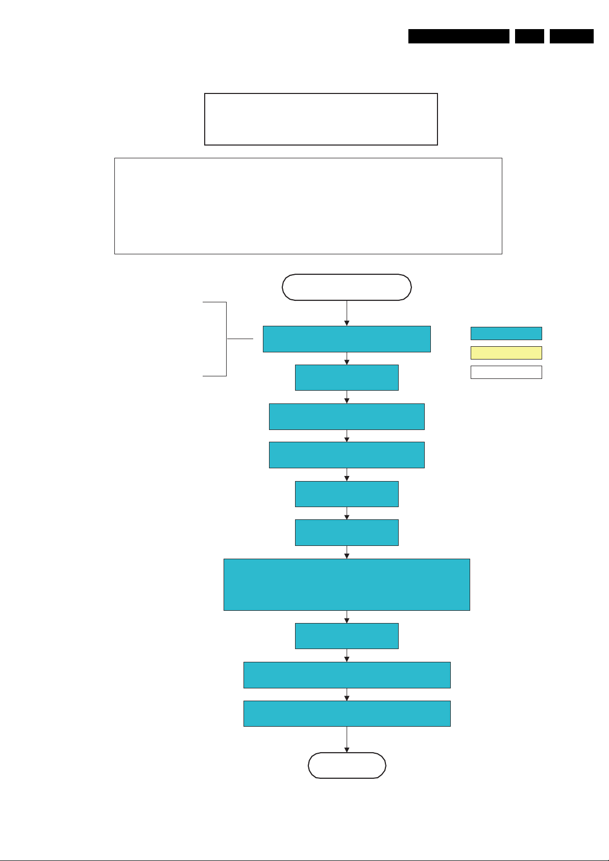
5.3 Stepwise Start-up
The stepwise start-up method, as known from FTL/FTP sets is
not valid any more. The situation for this chassis is as follows:
when the TV is in a protection state detected via the Stand-by
Processor (and thus blinking an error) and SDM is activated via
short cutting the pins on the SSB, the TV starts up until it
reaches the situation just before protection. So, this is a kind of
automatic stepwise start-up. In combination with the start-up
diagrams below, you can see which supplies are present at a
certain moment.
Important to know here is, that if e.g. the 3V3 detection fails
(and thus error 11 is blinking) and the TV is restarted via SDM,
the Stand-by Processor will enable the 3V3, but will not go to
protection now. The TV will stay in this situation until it is reset
(Mains/AC Power supply interrupted).
• SP: protection or error detected by the Stand-by
Processor.
• MP: protection or error detected by the VIPER Main
Processor.
The abbreviations “SP” and “MP” in the figures stand for:
- WakeUp requested
- Acquisition needed
Stand-by
(Off St-by)
- POD Card remove
- Tact SW pushed
- No data Acquisition required
and no POD present
- Tact SW pushed
d
Stand-by
On
Only applicable for sets with CableCARDTM slot (POD)
*
Mains
“off”
- WakeUp requested
- Acquisition needed
POD
*
Off
Semi
Stand-by
No data Acquisition
required and
POD present
GoToProtec
Mains
“on”
GoToProtection
tion
WakeUp
requested
- St-by requested
- Tact SW pushed
WakeUp
requested
Protection
Active
GoToProtection
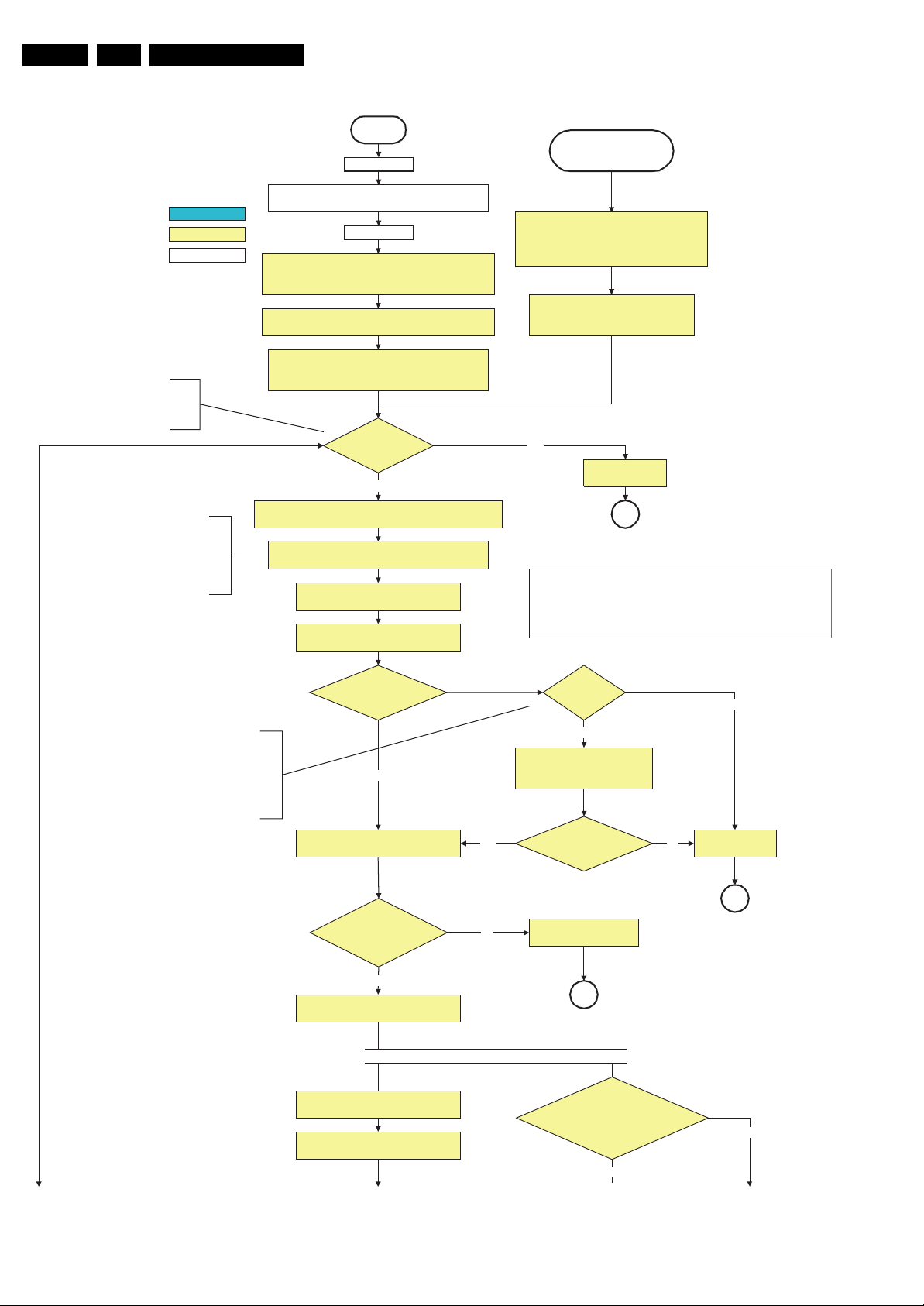
F_15400_095.eps
020206
Figure 5-4 Transition diagram
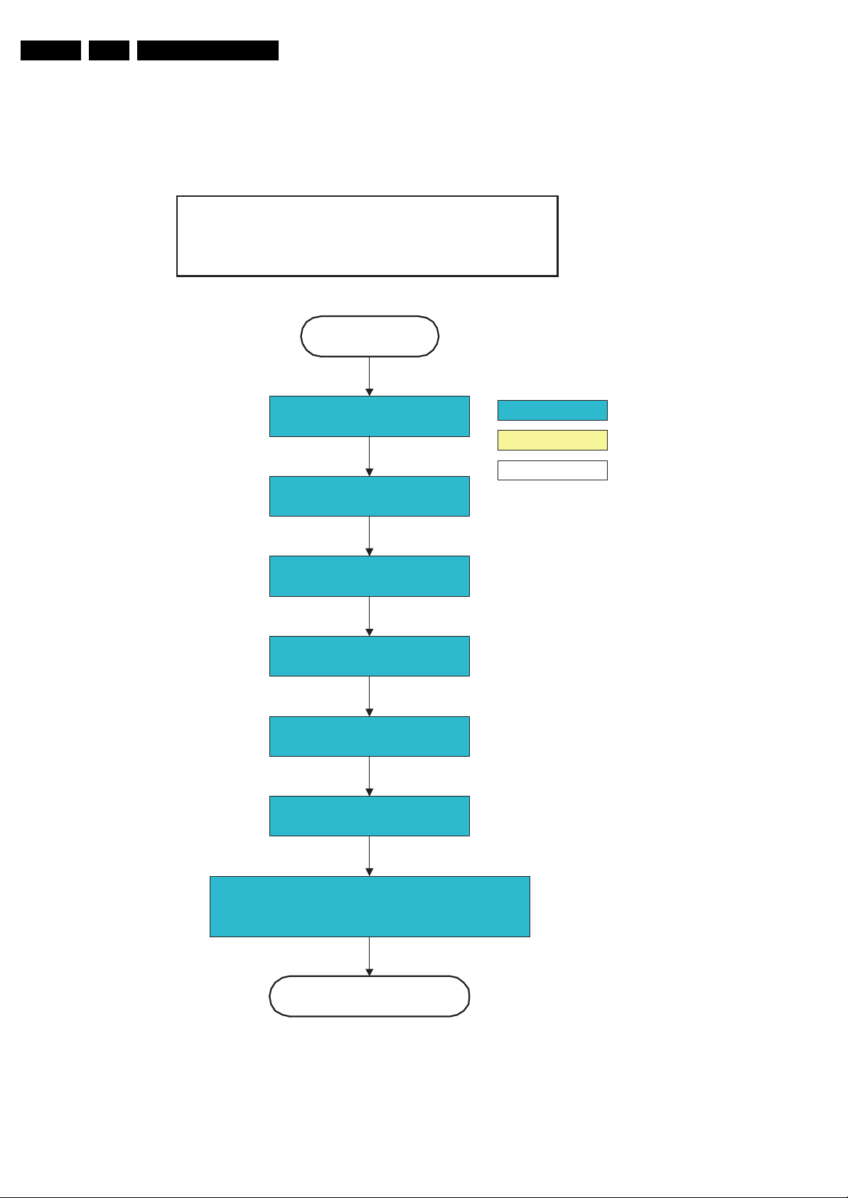
Page 18
EN 18 EJ2.0U LA5.
Service Modes, Error Codes, and Fault Finding
action holder: MIPS
action holder: St-by
autonomous action
The audio protection circuit shuts down the
supply autonomously. This triggers a set restart
and during that restart (so at this check here), it
will be observed that the audio protection line is
high and the audio protection mode is entered.
Switching on the power supply in an LPL scanning
backlight set, also switches on the backlight supply.
The display should not be used the first 5 seconds
the backlight supply is running due to a pre-heat
time of 4s and a 100% light output (not adjustable)
the next second. This 5 second delay does not
delay the startup of the display as this time is
absorbed in the startup time of the rest of the
system.
Off
Mains is applied
Standby Supply starts running.
+5V2, 1V2Stb, 3V3Stb and +2V5D become present.
In case o f PDP 3V3 Vpr to CPU PDP become s presen t.
st-by µP resets
All I/O lines have a High default state:
- Sound-Enable and Reset-Audio should remain high.
- NVM power line is high, no NVM communication possible
Initialise I/O pins of the st-by µP, start keyboard scanning,
RC detection, P50 decoding. Wake up reasons are off.
PDPGO line is high (either HW wise in a non FHP set or
because of the stby µP reset in a FHP set) which is the good
Switch LOW the NVM power reset line. Add a 2ms delay before
trying to address the NVM to allow correct NVM initialization.
Switch Main Supply to ON by switching LOW both the
- Assert the Viper reset
state at cold boot to be able to start the FHP.
Audio Protection Line
HIGH?
No
ON-MODE and the POD-MODE I/O lines.
+5V, Vtu n, +8V6 , +12VSW, +5V2S, Vsou nd
and +12/24V are switched on
Wait 50ms and then start polling the detect-
5V, detect-8V6 and detect-12V every 40ms.
Stand by or
Protection
If the protection state was left by short circuiting the
SDM pins, detection of a protection condition during
startup will stall the startup. Protection conditions in a
playing set will be ignored. The protection mode will
- Switch Sound-Enable and Reset-Audio high.
Yes
not be entered.
They are low in the standby mode if the
standby mode lasted longer than 10s.
Audio Error
SP
The availability of the supplies is checked through detect signals (delivered by
dedicated detect-IC's) going to the st-by µP. These signals are available for
+12V, +8V6, +5V, +1V2 and +2V5. A low to high transition of the signals should
occur within a certain time after toggling the standby line. If an observers is
detected before the time-out elapses, of course, the process should continue in
order to minimize start up time.
- Only when the PDPGO is low, a retry should be
considered (the PDP could have reset internally). If
the PDPGO is already high, there is no use in trying
to restart.
- PDPGO line is pulled high in all non FHP sets so
this extra startup delay in case of a fault condition
is not valid.
- Switching the PDPGO high will give a visual
artefact and should only be done if really
necessary.
detect-5V
received within
2900 ms after POD-MODE I/O
line toggle?
Yes
activate +5V supply detection algorithm
detect-12V received within
2900 ms after POD-mode I/O
line toggle?
Yes
activate +12V supply
detection algorithm
No need to wait for the 8V6 detection at this point.
Enable the DC/DC converter for +1.2V.
Start polling the detect-1V2 every 40ms
PDPGO
=
High?
No
Switch PDPGO hig h:
PDP should start: 5V, 8V6 and
12V are activated
detect-5V
yes
received within
2900 ms after PDPGO
toggle?
No
Yes
+5V erro r
SP
No
+12V error
SP
detect-8V6 received
within 6300 ms after POD-mode I/O line
toggle? Startup shall not wait for this
detection and continue startup.
Yes
To Part BTo Part C To Part B To Part B
Figure 5-5 “Off” to “Semi Stand-by” flowchart (part 1)
No
G_15990_103a.eps
100506
Page 19
Service Modes, Error Codes, and Fault Finding
EN 19EJ2.0U LA 5.
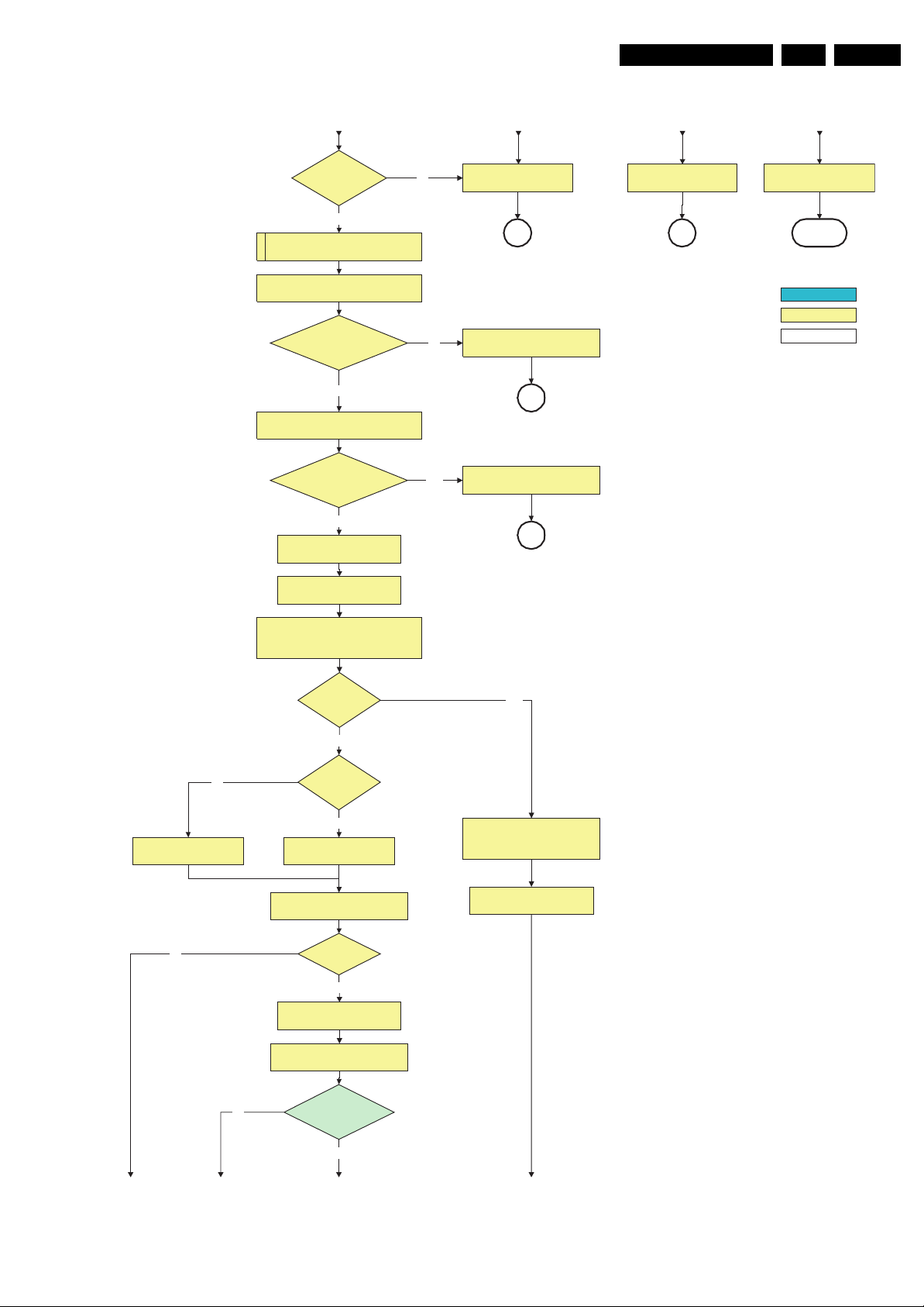
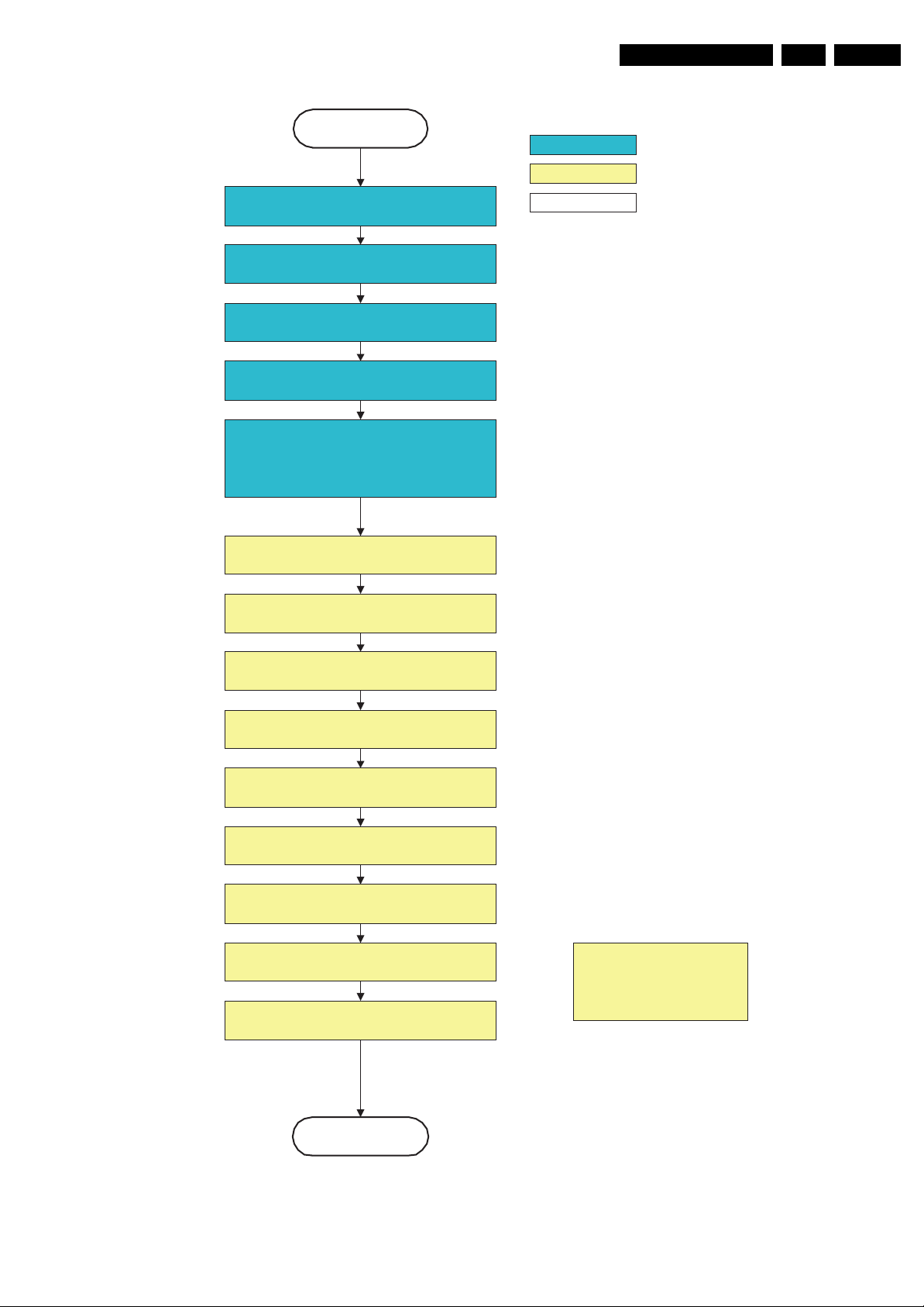
From Part A
detect-1V2
received within
250ms?
Yes
Enable the DC/DC converters for
+2.5V and +3.3V.
Start polling the detect-2V5
and detect-3V3 every 40ms
detect-2V5 and
detect-3V3 received within
250 ms?
Yes
Activate supply detection algorith ms for
+1.2V, +2.5 V and +3 .3V
SUPPLY-FAULT I/O lin e
is High?
No
Enable the supply fault detection
interru pt
From Part A From Part A From Part A
No
+1.2V err or
SP
+2.5V or +3.3V errorNo
+8V6 err or
SP
activate +8V6 supply
detection algorithm
return
action holder: MIPS
action holder: St-by
autonomous action
SP
Supply fault errorYes
SP
No
Release vipe r reset
Feed warm boot script(2)
No
Set I²C slave address
of Standby µP to (A0h)
Detect EJTAG debug probe
(pulling pin of the probe interface to
ground by inserting EJTAG probe)
EJTAG pro be
connected ?
No
Cold boot?
Yes
Release viper rese t
Feed cold boot script(1)
Release PNX2015 reset 100ms after
Viper reset is released
Bootscript ready
in 1250 ms?
Yes
Set I²C slave address
of Standby µP to (64h)
Yes
Release viper reset
Feed initializing boot script (3)
disable alive mechanism
Release PNX2015 reset 100ms
after Viper reset is released
RPC start (comm. protocol)
No
Flash to Ram image
transfer succeeded
wit hin 30 s?
Yes
To Part CTo Part CTo Part C To Part C
G_15990_103b.eps
100506
Figure 5-6 “Off” to “Semi Stand-by” flowchart (part 2)
Page 20
EN 20 EJ2.0U LA5.
Service Modes, Error Codes, and Fault Finding
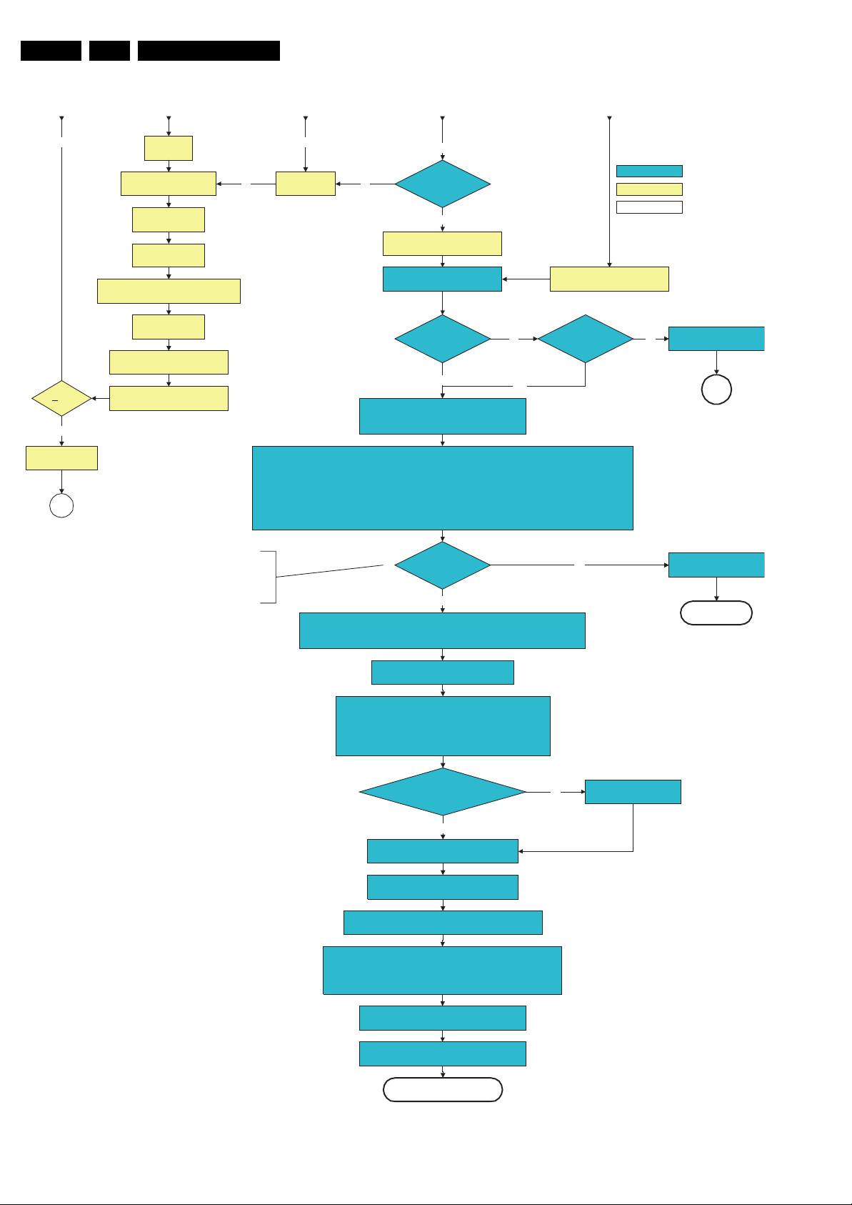
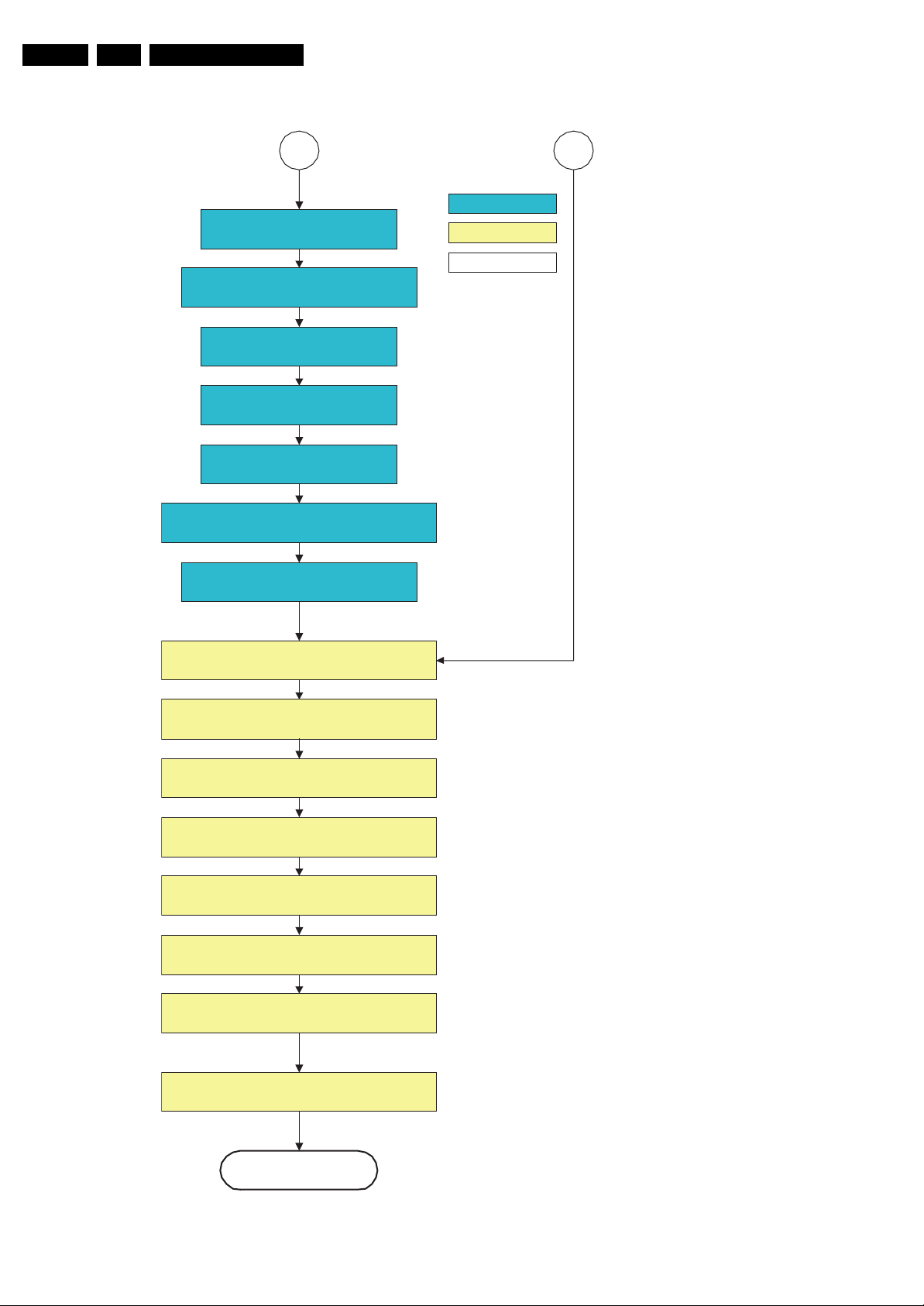
From Part BFrom Part A From Part B From Part B From Part B
3-th retry?
Yes
Log Code as
error code
SP
Code = 5
Switch Viper in reset
Wait 10ms
Switch the NVM reset
line HIGH.
Disable all supply related protections and
switch off the +2V5, +3V3 DC/DC converter .
Wait 5ms
switch off the remaining DC/DC
converters
Switch POD-MODE and ON-MODE
I/O line high.
Because of a bug in the Pacific IC, it will
very rarely not startup properly. If this
happens, only a cold boot can solve this
(removal of power supplies). Since this is
not feasible in the current SW
architecture, instead Standby mode is
entered.
NoNo
No
Code = 53
- Register PIIConfig of the Pacific3:
- in case of a non 1080p display, the LVDS bit should be set to 0 (CMOS input).
- in case of a 1080p display, the LVDS bit and the Dual Bus bit should be set to 1 (double lvds input).
- POIConfig of the Pacific3:
- in case of a non 1080p display, the LVDS bit should be set to 1 with the Dual Bus bit set to 0 (lvds out)
- in case of a 1080p display, the LVDS bit and the Dual Bus bit should be set to 1 (double lvds out)
- PanelConfig register: PanelOff = 0, PanelOn = 1. P3 can always be on, switching of lvds is done through PNX.
(AVIP's need to be started before the MPIF's in order to have a good clock distribution).
AVIP default power-up mode is Standby. The Viper instructs AVIP via I²C to enable all the
PLL's and clocks and h ence enter to Full Power mode. See FMS AVIP for further details
and the rest of the initialization.
No
Wait for the +8V6 to be detected if not yet present. (if
it does not come, the standby µP will en ter a
protection mode, this is not a dead end here)
Yes
Viper SW initializati on
succeeded
wit hin 20s ?
Yes
Enable Alive check mechanism
MIPS reads the wake up reason
from standby µP.
Set is
SDI PDP
or
FHP PDP?
Yes
Was Pacific responding
to I²C?
yes
No
Yes
Wait until Viper starts to
communicate
Power OK-display is
Hig h?
No
action holder: MIPS
action holder: St-by
autonomous action
Log display errorNo
MP
Log Pacific error and
Go to Standby
Standby
initialize PNX2015 HD subsyst em
MPIF's should be initialized.
MPIF should deliver 4 observers:
POR= 0; normal operation
MSUP = 1: Main supply is present
ASUP = 1; audio supply is present
ROK = 1; reference frequency is present (coming from AVIP)
All observers present with correct state?
Yes
initialize tuners and Hirate .
Initialize source select ion.
Initialize video processing IC's :
- Spider
initialize Columbus
initialize 3D Combfilte r
initialize AutoTV
Initialize Pacific related Ambilight settin gs
(if applicable)
Initialize Ambilight with Lights off.
No
Log appropriate
Observer error
Semi-Standby
Figure 5-7 “Off” to “Semi Stand-by” flowchart (part 3)
G_15990_103c.eps
120506
Page 21
Service Modes, Error Codes, and Fault Finding
Constraints taken into account:
- Display may only be started when valid QV CP output clock can be delivered by the Viper.
- Between 0 and 20 ms after power is supplied, display should receive valid lvds clock.
- minim um wait tim e to switch on the lam p after power up is 200m s.
- RGB (on QVCP output) may be unblanked before valid output is available. Unblanking of the
picture happens with the use of the 'lamp on', not with the RGB. By doing so, black level
differences during startup are avoided.
The assumption here is that a fast toggle
(<1s) can only happen during ON->SEMI
->ON. In these states, the Viper is still
active and can provide the 1s delay. If
the transition ON->SE MI ->STBY->SE MI-
>ON can be made in less than 1s, we
have to delay the semi -> stby transition
until the requirem ent i s m et.
37" 1366*768 LCD SHARP
Semi Standby
Wait until previous on-state is left more than 1
second ago. (to prevent LCD display problems)
Assert RGB video blanking
and audio m ut e
EN 21EJ2.0U LA 5.
action holder: MIPS
action holder: St-by
autonomous action
Initialize audio and video processing IC's and
functions according needed use case.
Wait until QVCP generates a valid lvds output
Switch off RGB blanking
Start to apply valid interface signals to the module (LVDS) within a time
frame of min. 17.5ms to max. 37.5ms after supply switch on.
In implementation, use 25ms, this makes it compatible with 37HD"Sharp
(t=17.5ms is the supply switch-on delay taken into account)
wait 250ms (min. = 200ms)
Switch on LCD lamp after valid, stable video, corresponding
to the requested output is delivered by the Viper
clock.
This unblank is moved forwards on demand
of SW to allow to obtain valid QVCP output
Switch on LCD supply
(LCD-Power-on)
(lamp ready delay)
Switch Audio-Reset and sound enable low and demute
(see CHS audio LdspMute interface).
Active
Figure 5-8 “Semi Stand-by” to “Active” flowchart
G_15940_045.eps
240506
Page 22
EN 22 EJ2.0U LA5.
Service Modes, Error Codes, and Fault Finding
37" 1366*768 LCD SHARP
Active
Mute all sound outputs.
Switch reset-audio and sound-enable
lines high
switch off LCD lamp
Mute all video outputs
Wait 0ms. (No need to wait here
for the 37" Sharp panel)
Switch off LVDS signal
action holder: MIPS
action holder: St-by
autonomous action
Switch off 12V LCD supply within a time frame of max.
1000ms after LVDS switch off.
(Viper I/O: LCD_ PWR_ON)
Semi Standby
Figure 5-9 “Active” to “Semi Stand-by” flowchart
G_15940_046.eps
240506
Page 23
Service Modes, Error Codes, and Fault Finding
EN 23EJ2.0U LA 5.
Semi Stand by
Delay transition until ramping down of ambient light is
finished. *)
Switch ambient light to passive mode with RGB
values on zero. *)
transfer Wake up reasons to the Standby µP.
Images are re-transferred to DDR-RAM from
Flash RAM (verification through checksum)
MIPS image completes the application reload,
stops DDR-RAM access, puts itself in a
sleepmode and signals the standby µP when the
standby mode can be entered.
DDR-RAM is put in self refresh mode and the images
are kept in the hibernating DDR-RAM.
action holder: MIPS
action holder: St-by
autonomous action
*) If this is not performed and the set is
switched to standby when the ramping of
the EPLD is still ongoing, the lights will
remain lit in standby.
Wait 5ms
Switch Viper in reset state
Wait 10ms
Switch the NVM reset line HIGH.
Disable all supply related protections and switch off
the +2V5, +3V3 DC/DC converter.
Wait 5ms
switch off the remaining DC/DC converters
Switch OFF all supplies by switching HIGH the POD-
MODE and the ON-MODE I/O lines.
Important remark:
release reset audio and sound-
enable 10 sec after entering
standby to save power
Stand by
Figure 5-10 “Semi Stand-by” to “Stand-by” flowchart
G_15990_108.eps
100506
Page 24
EN 24 EJ2.0U LA5.
Service Modes, Error Codes, and Fault Finding
MP
Log the appropriate error and
set stand-by flag in NVM
redefine wake up reasons for protection
state and transfer to stand-by µP.
switch off LCD lamp supply
Wait 250ms (min. = 200ms)
Switch off LVDS signal
Switch off 12V LCD supply within a time frame
of min. 0.5ms to max. 50ms after LVDS switch
off.
Ask stand-by µP to enter protection state
SP
action holder: MIPS
action holder: St-by
autonomous action
Switch Viper in reset state
Wait 10ms
Switch the NVM reset line HIGH.
Disable all supply related protections and switch off
the +2V5, +3V3 DC/DC converter.
Wait 5ms
Switch off remaining DC/DC converters
Switch OFF all supplies by switching HIGH the POD-
MODE and the ON-MODE I/O lines.
Flash LED in order to indicate protection state*.
Protection
Figure 5-11 “Protection” flowchart
(*): This can be the standby LED or the ON LED
depending on the availability in the set under
discussion.
G_15990_112.eps
120506
Page 25

Service Modes, Error Codes, and Fault Finding
5.4 Service Tools
5.4.1 ComPair
Introduction
ComPair (Computer Aided Repair) is a service tool for Philips
Consumer Electronics products. ComPair is a further
development on the European DST (service remote control),
which allows faster and more accurate diagnostics. ComPair
has three big advantages:
1. ComPair helps you to quickly get an understanding on how
to repair the chassis in a short time by guiding you
systematically through the repair procedures.
2. ComPair allows very detailed diagnostics (on I
is therefore capable of accurately indicating problem areas.
You do not have to know anything about I
yourself because ComPair takes care of this.
3. ComPair speeds up the repair time since it can
automatically communicate with the chassis (when the
microprocessor is working) and all repair information is
directly available. When ComPair is installed together with
the Force/SearchMan electronic manual of the defective
chassis, schematics and PWBs are only a mouse click
away.
Specifications
ComPair consists of a Windows based fault finding program
and an interface box between PC and the (defective) product.
The ComPair interface box is connected to the PC via a serial
(or RS-232) cable.
For this chassis, the ComPair interface box and the TV
communicate via a bi-directional service cable via the service
connector(s).
The ComPair fault finding program is able to determine the
problem of the defective television. ComPair can gather
diagnostic information in two ways:
• Automatically (by communicating with the television):
ComPair can automatically read out the contents of the
entire error buffer. Diagnosis is done on I
ComPair can access the I
ComPair can send and receive I
the microcontroller of the television. In this way, it is
possible for ComPair to communicate (read and write) to
devices on the I
2
C/UART buses of the TV-set.
• Manually (by asking questions to you): Automatic
diagnosis is only possible if the microcontroller of the
television is working correctly and only to a certain extent.
When this is not the case, ComPair will guide you through
the fault finding tree by asking you questions (e.g. Does the
screen give a picture? Click on the correct answer: YES /
NO) and showing you examples (e.g. Measure test-point I7
and click on the correct oscillogram you see on the
oscilloscope). You can answer by clicking on a link (e.g.
text or a waveform picture) that will bring you to the next
step in the fault finding process.
By a combination of automatic diagnostics and an interactive
question / answer procedure, ComPair will enable you to find
most problems in a fast and effective way.
2
C/UART bus of the television.
2
C/UART commands to
2
C level) and
2
C commands
2
C/UART level.
TO
UART SERVICE
CONNECTOR
PC VCR I2CPower
9V DC
E_06532_021.eps
Figure 5-12 ComPair interface connection
How to Order
ComPair order codes:
• ComPair Software: ST4191.
• ComPair Interface Box: 4822 727 21631.
• AC Adapter: T405-ND.
• ComPair Quick Start Guide: ST4190.
• ComPair interface extension cable: 3139 131 03791.
• ComPair UART interface cable: 3122 785 90630.
Note: If you encounter any problems, contact your local
support desk.
5.4.2 LVDS Tool
Introduction
This service tool (also called “ComPair Assistant 1“) may help
you to identify, in case the TV does not show any picture,
whether the Small Signal Board (SSB) or the display of a Flat
TV is defective.
Furthermore it is possible to program EPLDs with this tool (Byte
blaster). Read the user manual for an explanation of this
feature.
Since 2004, the LVDS output connectors in our Flat TV models
are standardized (with some exceptions). With the two
delivered LVDS interface cables (31p and 20p) you can cover
most chassis (in special cases, an extra cable will be offered).
When operating, the tool will show a small (scaled) picture on
a VGA monitor. Due to a limited memory capacity, it is not
possible to increase the size when processing high-resolution
LVDS signals (> 1280x960). Below this resolution, or when a
DVI monitor is used, the displayed picture will be full size.
Generally this tool is intended to determine if the SSB is
working or not. Thus to determine if LVDS, RGB, and sync
signals are okay.
How to Connect
Connections are explained in the user manual, which is packed
with the tool.
EN 25EJ2.0U LA 5.
TO
I2C SERVICE
CONNECTOR
180804
How to Connect
This is described in the chassis fault finding database in
ComPair.
Caution: It is compulsory to connect the TV to the PC as
shown in the picture below (with the ComPair interface in
between), as the ComPair interface acts as a level shifter. If
one connects the TV directly to the PC (via UART), ICs will be
blown!
Note: To use the LVDS tool, you must have ComPair release
2004-1 (or later) on your PC (engine version >= 2.2.05).
For every TV type number and screen size, one must choose
the proper settings via ComPair. The ComPair file will be
updated regularly with new introduced chassis information.
How to Order
• LVDS tool (incl. two LVDS cables: 31p and 20p):
3122 785 90671.
• LVDS tool Service Manual:
3122 785 00810.
Page 26
EN 26 EJ2.0U LA5.
Service Modes, Error Codes, and Fault Finding
5.5 Error Codes
5.5.1 Introduction
The error code buffer contains all detected errors since the last
time the buffer was erased. The buffer is written from left to
right, new errors are logged at the left side, and all other errors
shift one position to the right.
When an error has occurred, the error is added to the list of
errors, provided the list is not full or the error is a protection
error.
When an error occurs and the error buffer is full, then the new
error is not added, and the error buffer stays intact (history is
maintained), except when the error is a protection error.
To prevent that an occasional error stays in the list forever, the
error is removed from the list after 50+ operation hours.
When multiple errors occur (errors occurred within a short time
span), there is a high probability that there is some relation
between them.
Basically there are three kinds of errors:
• Errors detected by the Stand-by Processor. These
errors will always lead to protection and an automatic start
of the blinking LED for the concerned error (see paragraph
“The Blinking LED Procedure”). In these cases SDM can
be used to start up (see chapter “Stepwise Start-up”). NOte
that it can take up to 90 seconds before the TV goes to
protection and starts blinking the error (e.g. error 53).
• Errors detected by VIPER that lead to protection. In this
case the TV will go to protection and the front LED will also
blink the error code number. Further diagnosis can be done
via ComPair.
• Errors detected by VIPER that do not lead to
protection. In this case the error will be logged into the
error buffer and can be read out via ComPair, via blinking
LED method, or in case you have picture, via SAM.
5.5.2 How to Read the Error Buffer
Use one of the following methods:
• On screen via the SAM (only if you have a picture). E.g.:
– 00 00 00 00 00: No errors detected
– 06 00 00 00 00: Error code 6 is the last and only
detected error
– 09 06 00 00 00: Error code 6 was first detected and
error code 9 is the last detected error
• Via the blinking LED procedure (when you have no
picture). See next paragraph.
•Via ComPair.
5.5.3 How to Clear the Error Buffer
Use one of the following methods:
• By activation of the “RESET ERROR BUFFER” command
in the SAM menu.
• With a normal RC, key in sequence “MUTE” followed by
“062599” and “OK”.
• If the content of the error buffer has not changed for 50+
hours, it resets automatically.
5.5.4 Error Buffer
In case of non-intermittent faults, clear the error buffer before
you begin the repair (before clearing the buffer, write down the
content, as this history can give you significant information).
This to ensure that old error codes are no longer present.
If possible, check the entire contents of the error buffer. In
some situations, an error code is only the result of another error
code and not the actual cause (e.g., a fault in the protection
detection circuitry can also lead to a protection).
There are several mechanisms of error detection:
• Via error bits in the status registers of ICs.
• Via polling on I/O pins going to the stand-by processor.
• Via sensing of analogue values on the stand-by processor.
• Via a “not acknowledge” of an I
2
C communication
Take notice that some errors need more than 90 seconds
before they start blinking. So in case of problems wait 2
minutes from start-up onwards, and then check if the front LED
is blinking.
Table 5-3 Error code overview
Error Description Error/Prot Detected by Device Defective module Result
1
I2C1
2
I2C2
2
3
I
C3
2
4
5 VIPER does not boot (hardware failure) P Stby µP PNX8550 Protection + Error blinking
6 5V supply P Stby µP Protection + Error blinking
8 1.2V DC/DC P Stby µP Protection + Error blinking
11 3.3V DC/DC P Stby µP Protection + Error blinking
12 12V supply P Stby µP Protection + Error blinking
14 Supply Class D amplifiers P Stby µP Protection + Error blinking
16 MPIF1 Main Supply E VIPER PNX3000 IF I/O Error logged
17 MPIF1 Audio Supply (ASUP) E VIPER PNX3000 IF I/O Error logged
18 MPIF1 ref freq E VIPER PNX3000 IF I/O Error logged
25 Supply fault P Stby µP Protection + Error blinking
27 Phoenix E VIPER PNX2015B HD subsystem Error logged
29 AVIP1 E VIPER PNX2015 AV input processor 1 Error logged
32 MPIF1 E VIPER KN10241C Analog Front End 1 Error logged
34 Tuner1 E VIPER Tuner 1 Error logged
37 Channel decoder E VIPER NXT2003 Error logged
43 Hi Rate Front End E VIPER TDA8751 HDMI Error logged
44 NVM P Stby µP see extra info
45 Columbus 1 E VIPER PNX2015 Comb filter Error logged
53 VIPER does not boot (software failure) P Stby µP PNX8550 Protection + Error blinking
63 PDP Display P VIPER Display Protection + Error blinking
C4
I
PVIPER
PVIPER
PStby µP
PVIPER
I2C1_blocked
I2C2_blocked
I2C3_blocked
I2C4_blocked
Protection + Error blinking
Protection + Error blinking
Protection + Error blinking
Protection + Error blinking
Page 27

Service Modes, Error Codes, and Fault Finding
EN 27EJ2.0U LA 5.
Extra Info
• Rebooting. When a TV is rebooting constantly due to
internal problems, most of the time no errors will be logged
or blinked. This rebooting can be recognized via a ComPair
interface and Hyperterminal (for Hyperterminal settings,
see paragraph “Stand-by software upgrade”). You will see
that the loggings which are generated by the main software
keep continuing. In this case (rebooting) diagnose has to
be done via ComPair.
• Error 1 (I
2
C bus 1 blocked). When this error occurs, the
TV will go to protection and the front LED will blink error 1.
Now you can partially restart the TV via the SDM shortcut
pins on the SSB. Depending on the software version it is
possible that this error will not work correct: in some
software versions error 34 was blinking in stead of error 1.
• Error 2 (I
2
C bus 2 blocked). When this error occurs, the
TV will go to protection and the front LED will blink error 2.
Now you can partially restart the TV via the SDM shortcut
pins on the SSB. Due to hardware restriction (I
the fast I
2
C bus) it will be impossible to start up the VIPER.
2
C bus 2 is
When this error occurs, the TV will probably keep
rebooting. Further diagnose has to be done via ComPair.
• Error 3 (I
on I
2
C bus 3 blocked). There are only three devices
2
C bus 3: VIPER, Stand-by Processor, and NVM. The
Stand-by Processor is the detection device of this error, so
this error will only occur if the VIPER or the NVM is blocking
the bus. This error will also blink when the NVM gives no
acknowledge on the I
2
C bus (see error 44). Note that if the
12 V supply is missing, the DC/DC supply on the SSB will
not work. Therefore the VIPER will not get supplies and
could block I
an error 3.
• Error 4 (I
2
C bus 3. So, a missing 12 V can also lead to
2
C bus 4 blocked). When this error occurs, the
TV will go to protection and the front led will blink error 4.
Now you can start up the TV via the SDM short-cut pins on
the SSB. The TV will start up and ignore the error.
Depending on the problem it is even possible that you have
picture.
• Error 5 (Viper does not boot). This error will point to a
severe hardware problem around the VIPER (supplies not
OK, VIPER completely dead, I
2
C link between VIPER and
Stand-by Processor broken, etc....).
• Error 12 (12 V error). Except a physical problem with the
12 V itself, it is also possible that there is something wrong
with the Audio DC Protection: see paragraph "Hardware
Protections" for this.
• Error 14 (Audio supply). This error is triggered in case of
DC voltage on the speakers or an overvoltage or a too big
voltage difference between the positive and negative audio
supply.
The mechanism for this error works as follows: when a
problem is detected, the audio-protection line will switch off
the main supply, the stand-by processor will “think” there is
a voltage drop and will start up the TV again. At the
beginning of the start up process the stand-by processor
will detect that the audio-protection line is still “active” and
will switch the TV to stand-by and blink error 14.
Note that for 26-inch models there no possibility to switch
off the main supply directly by the audio-protection line.
• Error 16 (MPIF1 main supply). This error is no longer
valid. See error 32.
• Error 17 (MPIF1 audio supply). This error is no longer
valid. See error 32.
• Error 27 (PNX2015 HD subsystem part). Diagnosing this
error will not be possible via the normal errorcodes. In case
this device can not communicate with the Viper via I
2
C, it
will not be possible to initialize the tunnelbus. Hence the
software will not be able to start up, and will reboot
constantly. Diagnosing these problems will only be
possible via ComPair. In theory it is possible that this error
is still logged in the NVM. That’s why it is still mentioned
here.
• Error 29 (AVIP1). Same remark as for error 27.
• Error 31 (AVIP2). Same remark as for error 27.
• Error 32 (MPIF1). Together with error 32, you will probably
see error 16 and 17. These errors are no longer valid.
• Error 34 (Tuner 1). When this error is logged, it is not sure
that there is something wrong with the tuner itself. It is also
possible that there is something wrong with the
communication between channel decoder and tuner. See
schematic B2B.
• Error 37 (Channel decoder). This error will always log
error 34 (tuner) extra. This is due to the fact that the tuner
2
I
C bus is coming from the channel decoder.
• Error 44 (NVM). This error will never occur because it is
masked by error 3 (I
for error 3 checks on an I
2
C bus 3). The detection mechanism
2
C acknowledge of the NVM. If
NVM gives no acknowledge, the stand-by software
assumes that the bus is blocked, the TV goes to protection
and error 3 will be blinking.
• Error 53. This error will indicate that the VIPER has started
to function (by reading his boot script, if this would have
failed, error 5 would blink) but initialization was never
completed because of hardware peripheral problems
(NAND flash,...) or software initialization problems.
Possible cause could be that there is no valid software
loaded (try to upgrade to the latest main software version).
5.6 The Blinking LED Procedure
5.6.1 Introduction
The blinking LED procedure can be split up into two situations:
• Blinking LED procedure in case of a protection. In this case
the error is automatically blinked. This will be only one
error, namely the one that is causing the protection.
Therefore, you do not have to do anything special, just read
out the blinks. A long blink indicates the decimal digit, a
short blink indicates the units.
• Blinking LED procedure in the “on” state. Via this
procedure, you can make the contents of the error buffer
visible via the front LED. This is especially useful for fault
finding, when there is no picture.
When the blinking LED procedure is activated in the “on” state,
the front LED will show (blink) the contents of the error-buffer.
Error-codes > 10 are shown as follows:
1. “n” long blinks (where “n” = 1 - 9) indicating decimal digit,
2. A pause of 1.5 s,
3. “n” short blinks (where “n”= 1 - 9),
4. A pause of approx. 3 s.
5. When all the error-codes are displayed, the sequence
finishes with a LED blink of 3 s,
6. The sequence starts again.
Example: Error 12 9 6 0 0.
After activation of the SDM, the front LED will show:
1. 1 long blink of 750 ms (which is an indication of the decimal
digit) followed by a pause of 1.5 s,
2. 2 short blinks of 250 ms followed by a pause of 3 s,
3. 9 short blinks followed by a pause of 3 s,
4. 6 short blinks followed by a pause of 3 s,
5. 1 long blink of 3 s to finish the sequence,
6. The sequence starts again.
5.6.2 How to Activate
Use one of the following methods:
• Activate the SDM. The blinking front LED will show the
entire contents of the error buffer (this works in “normal
operation” mode).
• Transmit the commands “MUTE” - “062500” - “OK”
with a normal RC. The complete error buffer is shown.
Take notice that it takes some seconds before the blinking
LED starts.
•Transmit the commands “MUTE” - “06250x” - “OK”
with a normal RC (where “x” is a number between 1 and
Page 28

EN 28 EJ2.0U LA5.
Service Modes, Error Codes, and Fault Finding
5). When x= 1 the last detected error is shown, x= 2 the
second last error, etc.... Take notice that it takes some
seconds before the blinking LED starts.
5.7 Protections
5.7.1 Software Protections
Most of the protections and errors use either the stand-by
microprocessor or the VIPER controller as detection device.
Since in these cases, checking of observers, polling of ADCs,
filtering of input values are all heavily software based, these
protections are referred to as software protections.
There are several types of software related protections, solving
a variety of fault conditions:
• Protections related to supplies: check of the 12V, +5V,
+8V6, +1.2V, +2.5V and +3.3V.
• Protections related to breakdown of the safety check
mechanism. E.g. since a lot of protection detections are
done by means of the VIPER, failing of the VIPER
communication will have to initiate a protection mode since
safety cannot be guaranteed anymore.
Remark on the Supply Errors
The detection of a supply dip or supply loss during the normal
playing of the set does not lead to a protection, but to a cold
reboot of the set.
Protections during Start-up
During TV start-up, some voltages and IC observers are
actively monitored to be able to optimize the start-up speed,
and to assure good operation of all components. If these
monitors do not respond in a defined way, this indicates a
malfunction of the system and leads to a protection. As the
observers are only used during start-up, they are described in
the start-up flow in detail (see paragraph “Stepwise Start-up").
5.7.2 Hardware Protections
There is one hardware protection in this chassis: “Audio DC
Protection”. This protection occurs when there is a DC voltage
on the speakers or an overvoltage or a too big voltage
difference between the positive and negative audio supply. In
that case the main supply is switched "off", but the stand-by
supply is still working. See also extra info for error 14.
In case of LCD supplies, the 12V supply will drop. This will be
detected by the stand-by processor, which will start blinking the
12 V error (error 12).
Repair Tip
• It is possible that you have an audio DC protection because
of an interruption in one or both speakers (the DC voltage
that is still on the circuit cannot disappear through the
speakers).
5.8 Fault Finding and Repair Tips
Read also paragraph "Error Codes" - "Extra Info".
5.8.1 Exit “Factory Mode”
When an "F" is displayed in the screen's right corner, this
means that the set is in "Factory" mode, and it normally
happens after a new SSB has been mounted.
To exit this mode, push the "VOLUME minus" button on the
TV's keyboard control for 5 seconds and restart the set
5.8.2 MPIF
Important things to make the MPIF work:
• Supply.
• Clock signal from the AVIP.
2
•I
C from the VIPER.
5.8.3 AVIP
Important things to make the AVIP work:
• Supplies.
• Clock signal from the VIPER.
2
•I
C from the VIPER (error 29 and 31).
5.8.4 DC/DC Converter
Introduction
• The best way to find a failure in the DC/DC converters is to
check their starting-up sequence at power "on" via the
Mains/AC Power cord, presuming that the Stand-by
Processor is operational.
• If the input voltage of the DC/DC converters is around 12 V
(measured on the decoupling capacitors 2U17/2U25/
2U45) and the ENABLE signals are "low" (active), then the
output voltages should have their normal values.
• First, the Stand-by Processor activates the +1V2 supply
(via ENABLE-1V2).
• Then, after this voltage becomes present and is detected
OK (about 100 ms), the other two voltages (+2V5 and
+3V3) will be activated (via ENABLE-3V3).
• The current consumption of controller IC 7U00 is around 20
mA (that means around 200 mV drop voltage across
resistor 3U22).
• The current capability of DC/DC converters is quite high
(short-circuit current is 7 to 10 A), therefore if there is a
linear integrated stabilizer that, for example delivers 1.8V
from +3V3 with its output overloaded, the +3V3 stays
usually at its normal value even though the consumption
from +3V3 increases significantly.
• The +2V5 supply voltage is obtained via a linear stabilizer
made with discrete components that can deliver a lot of
current. Therefore, in case +2V5 (or +2V5D) is shortcircuited to GND, the +3V3 will not have the normal value
but much less.
• The supply voltage +12VSW is protected for over-currents
by fuse 1U04.
Fault Finding
• Symptom: +1V2, +2V5, and +3V3 not present (even for a
short while ~10ms).
1. Check 12V availability (fuse 1U01, resistor 3U22,
power MOS-FETs) and enable signal ENABLE-1V2
(active low).
2. Check the voltage on pin 9 (1.5 V).
3. Check for +1V2 output voltage short-circuit to GND that
can generate pulsed over-currents 7-10 A through coil
5U03.
4. Check the over-current detection circuit (2U12 or 3U97
interrupted).
Page 29
Service Modes, Error Codes, and Fault Finding
EN 29EJ2.0U LA 5.
• Symptom: +1V2 present for about 100 ms. Supplies +2V5
and +3V3 not rising.
1. Check the ENABLE-3V3 signal (active "low").
2. Check the voltage on pin 8 (1.5 V).
3. Check the under-voltage detection circuit (the voltage
on collector of transistor 7U10-1 should be less than
0.8 V).
4. Check for output voltages short-circuits to GND (+3V3,
+2V5 and +2V5D) that generate pulsed over-currents
of 7-10 A through coil 5U00.
5. Check the over-current detection circuit (2U18 or 3U83
interrupted).
• Symptom: +1V2 OK, but +2V5 and +3V3 present for about
100 ms. Cause: The SUPPLY-FAULT line stays "low"
even though the +3V3 and +1V2 is available. The Stand-by
Processor is detecting that and switches all supply
voltages "off".
1. Check the drop voltage across resistor 3U22 (this
could be too high)
2. Check if the +1V2 or +3V3 are higher than their normal
values. This can be due to defective DC feedback of
the respective DC/DC converter (3U18 or 3UA7).
• Symptom: +1V2, +2V5, and +3V3 look okay, except the
ripple voltage is increased (audible noise can come from
the filtering coils 5U00 or 5U03).
Cause: Instability of the frequency and/or duty cycle of one
or both DC/DC converters.
– Check resistor 3U06, the decoupling capacitors, the
AC feedback circuits (2U20 + 2U21 + 3U14 + 3U15 for
+1V2 or 2U19 + 2U85 + 3U12 + 3U13 for +3V3), the
compensation capacitors 2U09, 2U10, 2U23 and
2U73, and IC 7U00.
Note 1: If fuse 1U01 is broken, this usually means a pair of
defective power MOSFETs (7U01 or 7U03). Item 7U00 should
be replaced as well in this case.
5.9.2 Main Software Upgrade
The software image resides in the NAND-Flash, and is
formatted in the following way:
Partition 1
Trimedia2 image
Trimedia1 image
MIPS image
Partition 0
USB Download Application
uBTM (boot block)
Figure 5-13 NAND-Flash format
Executables are stored as files in a file system. The boot loader
(uBTM) will load the USB Download Application in partition 0
(USB drivers, bootscript, etc.). This application makes it then
possible to upgrade the main software via USB.
Installing "Partition 0" software is possible via an external
EJTAG tool, but also in a special way with the USB stick (see
description in paragraph “Partition 0“).
Partition 1 (Customer)
To do a main software upgrade (partition 1) via USB, the set
must be operational, and the "Partition 0" files for the VIPER
must be installed in the NAND-Flash!
The new software can be uploaded to the TV by using a
portable memory device or USB storage compliant devices
(e.g. USB memory stick). You can download the new software
from the Philips website to your PC.
USB CUSTOMER
USB SERVICE
EJTAG
E_14700_082.eps
120505
5.9 Software Upgrading
5.9.1 Introduction
The set software and security keys are stored in a NAND-Flash
(item 7P80), which is connected to the VIPER via the PCI bus.
It is possible for the user to upgrade the main software via the
USB port. This allows replacement of a software image in a
standalone set, without the need of an E-JTAG debugger. A
description on how to upgrade the main software can be found
in chapter 3 "Directions For Use".
Important: When the NAND-Flash must be replaced, a new
SSB must be ordered, due to the presence of the security
keys!!! See table “SSB service kits” for the order codes.
Perform the following actions after SSB replacement:
1. Set the correct option codes (see sticker inside the TV).
2. Update the TV software (see chapter 3 for instructions).
3. Perform the alignments as described in chapter 8.
4. Check in CSM menu 5 if the HDMI keys are valid.
Table 5-4 SSB service kits
Model Number
37PF9631D/37 3104 328 46521 3104 328 47611
SSB factory assy code
1) Information in column “SSB factory assy code” is only for
reference purposes. Do not use this code when ordering a new
SSB!
1)
New SSB order code
Partition 0 (Service)
If the "Partition 0" software is corrupted, the software needs to
be re-installed.
To upgrade this “USB download application” (partition 0 except
the bootblock), insert an USB stick with the correct software,
but press the “red” button on the remote control (in ”TV” mode)
when it is asked via the on screen text.
Caution:
• The USB download application will now erase both
partitions (except the boot block), so you need to reload the
main SW after upgrading the USB download application.
As long as this is not done, the USB download application
will start when the set is switched “on”.
• When something goes wrong during the progress of this
method (e.g. voltage dip or corrupted software file), the set
will not start up, and can only be recovered via the EJTAG
tool!
Page 30

EN 30 EJ2.0U LA5.
5.9.3 Manual Start of the Main Software Upgrade Application
Normally, the software upgrading procedure will start
automatically, when a memory device with the correct software
is inserted, but in case this does not work, it is possible to force
the TV into the software upgrade application. To do so:
• Disconnect the TV from the Mains/AC Power.
• Press the “OK” button on a Philips DVD RC-6 remote
control (it is also possible to use the TV remote in "DVD"
mode).
• Keep the “OK” button pressed while connecting the TV to
the Mains/AC Power.
• The software upgrade application will start.
• When a memory device with upgrade software is
connected, the upgrade process will start.
5.9.4 Stand-by Software Upgrade
It will be possible to upgrade the Stand-by software via a PC
and the ComPair interface. Check paragraph "ComPair" on
how to connect the interface. To upgrade the Stand-by
software, use the following steps:
1. Disconnect the TV from the Mains/AC Power.
2. Short circuit the SPI pins [2] on the SSB. They are located
outside the shielding (see figure “SDM and SPI service
pads” earlier in this chapter).
3. Keep the SPI pins shorted while connecting the TV to the
Mains/AC Power.
4. Release the short circuit after approx. two seconds.
5. Start up HyperTerminal (can be found in every Windows
application via Programs -> Accessories ->
Communications -> HyperTerminal. Use the following
settings:
–COM1
– Bits per second = 38400
– Data bits = 8
– Parity = none
– Stop bits = 1
– Flow control = Xon / Xoff.
6. Press “Shift U” on your PC keyboard. You should now see
the following info:
– PNX2015 Loader V1.0
– 19-09-2003
– DEVID=0x05
–Erasing
– MCSUM=0x0000
–=
7. If you do not see the above info, restart the above
procedure, and check your HyperTerminal settings and the
connections between PC and TV.
8. Via “Transfer” -> “Send text file ...”, you can send the
proper upgrade file to the TV. This file will be distributed via
the Service Organization.
9. After successful programming, you must see the following
info:
– DCSUM=0xECB3
–:Ok
– MCSUM=0xECB3
– Programming
– PCSUM=0xECB3
– Finished
10. If you do not see this info, restart the complete procedure.
11. Close HyperTerminal.
12. Disconnect and connect Mains/AC Power again.
Service Modes, Error Codes, and Fault Finding
Page 31

Block Diagrams, Test Point Overviews, and Waveforms
6. Block Diagrams, Test Point Overviews, and Waveforms
Wiring Diagram
WIRING 37” LCD
EN 31EJ2.0U LA 6.
RIGHT
SPEAKER
8740
INVERTER
AMBI LIGHT
AL
(IN BACK COVER)
3P
1M16
11P
1M11
1M39
1M59
1M49
3P
5P
4P
14P
8319
8320
SA
14P
1316
1M02
B
STANDBY
14P
1319
4P
7P
1740
SSB
1H07
14P
EJTAG
10P13
1J02
8102
4P
1M49
3P
4P
1309
8549
1304
4P
1M60
4P
1M10
8309
31P
1G50
8M60
1M46
11P
1306
1307
1305
1M03
2P3
4P
3P
10P
3P
1M01
8304
8305
8150
1M21
6P
LV DS
30P
11P
1M36
8509
8136
8306
LCD SUPPLY
A
2P3
1306
3P
1305
8740
3P
1309
8508
1304
4P
8302
7P
1M02
8539
INVERTER
AMBI LIGHT
AL
(IN BACK COVER)
6P
1M08
4P
1M09
6P
1M10
4P
1M49
5P
1M59
3P
1M39
14P
1M13
1M15
1M11
1M16
11P
3P
11P
3P
LEFT
SPEAKER
SIDE I/O
D
4P
1M60
KEYBOARD CONTROL
E
1M01
3P
3P
11P
1M15
1M13
1M10
1M09
1M08
4P6
4P
6P
8101
1M16
3P
Compair
Tu ne r
1308
2P3
8408
AC INLET
8195
8121
8310
11P
IR/LED/LIGHT
J
SENSOR
G_15940_034.eps
2P3
1M36
6P
1870
1M65
220506
Page 32

Block Diagrams, Test Point Overviews, and Waveforms
Block Diagram Supply
SUPPLY 37"
MAINS FILTER + STANDBY
A1
1308
2
1
MAINS INPUT
95-264Vac
1314
T5AH
5305
5306
MAINS
FILTER
3
1
1350
EN 32EJ2.0U LA 6.
SUPPLY
A2
14
7002
BIAS SUPPLY
VCC
3000
15
14
OA
12
OB
10
FI
5017
5001
4
2
7007
6
7
7008
10
9
2319
3318
2
4
6307
GBJ6J
-
+
399V_HOT
6318
9311
25V_HOT
6315
6316
14
2
6317
6314
RES
7307
TCET1102
3
6304
5007
5008
25V_HOT
400V_HOT
399V_HOT
7011
7012
SOFT
START
+
CURRENT
PROTECTION
3007
7001
MC34067P
11
OSCC
CONTROL
7
ERROR
11
SOST
5
VREF
7004
7009
PROTECTION
OVER
VOLTAGE
HIGH
SIDE
DRIVE
LOW
SIDE
DRIVE
2003
5009
STP15NK50
60246025
7005
7006
STP15NK50
PRINTED
COMPONENT
5010
400V_HOT
2059
5012
2060
TCET1102
2
3
5011
5002
5025
5026
7003
3057
3031
DC_PROT
6019
STPS20L40CFP
6019
STPS20L40CFP
2029
6021
6041
2045
5021
3030
7010
TS2431
2042
6031
3052
3025
2020
VS Voltage
Adj.
3026
2022
+12V
+24Va
+24Vb
1304
44
33
22
11
SA1
1304
CONNECTIONS
+12V_A
+12V_+24V
1316
1319
1M10
1
2
3
4
5
1
2
3
4
5
1
2
TO
DISPLAY
TO
DISPLAY
TO 1M10
AL
AMBI LIGHT
(OPTIONAL)
6306
DF06M
-
6040
2512
2049
2009
6029
6030
2021
+12V_A
5507
STANDBY: LOW = ON
HIGH = STBY
7531
5020
5018
5019
7131
STANDBY
VSND_POS
GND_SND
VSND_NEG
+5V2-RELAY-IO2_PWM
VTUN
+11V
+12V
+8V6
RES
+5V2
+5V_SW
DC_PROT
1M02
7
6
5
TO 1M02
4
B08B
3
AUDI O
2
1
1M03
TO 1J02
9
B01B
B01B
4
SUPPLY
1M46
11
9
TO 1J02
1
B01B
B01B
2
SUPPLY
7
G_15940_035.eps
220506
5022
1007
T5A
HOT GROUND
COLD GROUND
2303
1315
T1A
+
1305
11
22
33
1306
11
22
SA2
1305
1306
1307
STANDBY
1
2
3
4
RES
+5V2
CONTROL
7505/7509/7560
5504
5505
Prot-OVV
PROT_AUDIOSUPPLY
SA2
SA1
7100
7101
7105
CONTROL
6153
3101
3104
3150
3127
3100
6150
STP15NK50
6151
7102
3155
5104
3V MAX
1V MAX STBY
3108
3156
6156
HOT GROUND COLD GROUND
HOT GROUND COLD GROUND
COLD
HOT
5500
5
3
2
1
5105
14
7501
TCET1102
2
3
14
7150
3157
TCET1102
2
3
RES
7507
7506
7512
STANDBY
7511
6504
6140
3124
PROT-OVV
3509
5103
6122
OVERVOLTAGE
PROTECTION
6107
2513
3113
RES
2141
5506
5110
6
7
8
10
3128
3158
Page 33

Block Diagrams, Test Point Overviews, and Waveforms
Block Diagram Video
VIDEO
MAIN TUNER
B02B
1T04
TD1336O/FGHP
MAIN HYBRID
TUNER
CHANNNEL DECODER
B02A
7T22
NXT2004
DTV CABLE AND
TERRESTRIAL
RECEIVER
QAM 8VSB
Demodulator
FEC
Micro-
Controller
QPSK
Demodulator
MPEG_DATA
SIDE I/O
D
VIDEO
S VIDEO
ANALOG I/O
B07C
PR
PB
AV1
Y
VIDEO
IN
PR
PB
AV2
Y
VIDEO
IN
VIDEO
AV3
S VIDEO
IF-OUT
IF-1
IF-2
FM-T
IF-AGC
34
38
8
7
ADC
ADC
48
GPIO
84
ADC
29
30
DV1F-DATA(0-7)
1002
1001
1
3
5
4
2
1I04
1I03
1I00
1I01
1
3
5
4
2
12
1T01
14
1
15
14
SAW 44MHz
4
13
FAT-IF-AGC-MAIN
AUX-IF-AGC
FAT-ADC-INN
FAT-ADC-INP
FM-TRAP
IRQ-FE-MAIN
1T11
25M14
B05C
VIPER
IF-ANA
TO
Y-CVBS
7T13
LA7795T-E
2
7
8
3
in
AGC COTROL
C
AV7_Y-CVBS
AV1_CVBS
AV2_Y-CVBS
AV2_ C
PR1
EN 33EJ2.0U LA 6.
PMX-MA
B05
VIPER:
7V00
PNX8550
AH19
AG25
MP-OUT-HS
MP-OUT-VS
MP-CLKOUT
MP-OUT-FFIELD
MP-OUT-DE
7L50
K4D261638F
45
46
B05C B05B
TUNNELBUS
MAIN MEMORY
VIPER
Tunnel
B05C
AUDIO/VIDEO
2-Layer
secondary
video out
Dual SD
single HD
MPE2 decoder
250Mhz
MIPS32
CPU
Scaler and
de-interlacer
1SD+1HD
YUV
Video in
Video
TS
router
Dual
con
acces
TXPNXA-
TXPNXA+
TXPNXB-
TXPNXB+
TXPNXC-
TXPNXC+
TXPNXCLK-
TXPNXCLK+
TXPNXD-
TXPNXD+
TXPNXE-
TXPNXE+
DDR
SDRAM
128Mx16
Memory
controller
DVD
CSS
2D DE
Temporal
noise redux
B05A
CONTROL
5 Layer
primary
video out
HD/VGA/
MP-HS
MP-VS
MP-CLK
MP-FF
MP-DE
MP-R(0-7)MP-ROUT(0-9)
MP-G(0-7)MP-GOUT(0-9)
MP-B(0-7)MP-BOUT(0-9)
MM_DATA
MM_A(0-12)
C4
1H00
A2
27M
DV-RO UT
DV-GOUT
656
DV-BO UT
VIPER/PNX 2015:
B04G
DISPLAY INTERFACE
VDISP
5J50
5J52
5J54
5J56
5J58
5J60
SCL-I2C4
SDA-I2C4
MPIF MAIN:
B03
1A10
7
CVBSOUTIF-MAIN
AV1_CVBS
AV2_Y-CVBS
AV7_Y-CVBS
FRONT_Y-CVBS
FRONT_C
HDMI +SUPPLY
1
18 2
19
HDMI
2
4
AV2_ C
1I06
10
12
15
16
19
1B02
7A11
EF
1
3
4
6
7
9
8
5
ARX-HOTPLUG
3A17
IF-ANA
7
6
out
7T12
N.C.
B07C
1M36
B07C
B07C
1M36
2
2
4
4
B05A
B07A
PB1
PR
B07b
B07b
Y1
B07b
B03a
B07b
PB
B07b
Y
B07b
B03a
B03a
B03a
B07A
B07A
B07A
B07A
B07A
B07A
B07A
B07A
CONNECTOR
N.C.
N.C.
107
108
99
100
120
123
126
1
12
5
8
9
15
16
25
26
27
30
31
32
ARX2+
ARX2-
ARX1+
ARX1-
ARX0+
ARX0-
ARXC+
ARXC-
ARX-DCC-SCL
ARX-DCC-SDA
7B20
HPD-HIRATE
H-SYNC-VGA
V-SYNC-VGA
7A00
PNX3000HL
B03C
IF
VIFINP
VIFINN
SIFINP
SIFINN
CVBSOUTIF
B03A
SOURCE SELECTION
CVBS-IF
CVBS1
CVBS2
CVBS_DTV
CVBS|Y34
C3
CVBS|Y4
C4
Y_COMB
C_COMB
R|PR|V_1
YUV
G|Y|Y_1
RGB
B|PB|U_1
R|PR|V_2
G|Y|Y_2
B|PB|U_2
B07B
B05A
Y
Y1
PR
PR1
Y
Y1
PB
PB1
SOUND
LPF
BPF
LPF
CVBS/Y RIM
LC
C-PRIM
+
CVBS SEC
LEVEL
ADAPT
CLAMP
INV.
PAL
HDMI: I/O + CONTROL
7B50
TDA9975HS
180
RX2+A
179
RX2-A
174
RX1+A
Termination
173
RX1-A
resistance
168
RX0+A
167
162
161
131
128
control
RX0-A
RXC+A
RXC-1
RX2+B
RX2-B
RX1+B
Termination
RX2-B
resistance
control
RX0+B
RX0-B
RXC+B
RXC-B
HSCL B
HSDA B
Line time
measuremebt
Activity
HSYNC
detection &
VSYNC
sync selec.
90
88
G/Y
Slicers
96
R/PR
94
81
79
68
66
G/Y
B/PB
ADC
TRAP
A
M
CLAMP
GROUP
DELAY
QSS
TO AM INTERNAL
AUDIO SWITCH
LPF
P
LPF
Yyuv
U
V
MONO SEC.
HDMI
receiver
QSSOUT
LPF
A
D
Yyuv
2FH
2nd
SIF
A/D
A
D
A
D
CLP PRIM
CLP SEC
CLP yuv
HDMI
Derepeater
Sync
seperator
Clocks
generator
A
D
Yyuv
2Fh
U,V
Upsample
HDCP
MPIF
DATA
LINK
1
DATA
LINK
3
DATA
LINK
2
TIMING
CIRCUIT
B03B
SUPPLY
SUPPLY
DIGITAL
BLOCK
CVBS-OUTA
CVBS-OUTB
STROBE1N
STROBE1P
DATA1N
DATA1P
STROBE3N
STROBE3P
DATA3N
DATA3P
STROBE2N
STROBE2P
DATA2N
DATA2P
Video
output
formatter
VHREF
timing
generator
I2C slave
interface
14
28
35
44
43
19
22
60
61
62
63
50
51
52
53
55
56
57
123
46
40
2
1
201
207
142
143
SCL-DMA
SDA-DMA
N.C.
N.C.
STROBE1N-MAIN
STROBE1P-MAIN
DATA1N-MAIN
DATA1P-MAIN
STROBE3N-MAIN
STROBE3P-MAIN
DATA3N-MAIN
DATA3P-MAIN
STROBE2N-MAIN
STROBE2P-MAIN
DATA2N-MAIN
DATA2P-MAIN
HV-PRM-MAIN
N.C.
N.C.
DV4- DATA(0- 7)
DV5- DATA(0- 7)
DV4- CLK
DV-HREF
DV-VREF
DV-FREF
SDA-MM
SCL-MM
PNX 2015: STANDBY
B04E
& CONTROL
7LA7
M25P05
512K
FLASH
+5V
CLK-MPIF
AV2_FBL
AV6_VSYNC
5
6
1
3
SPI-SDO
SPI-CLK
SPI-CSB
SPI-WP
1LA0
16M
B04
AK10
AH10
AG10
AJ27
AH12
AK8
AJ12
AH9
AK9
R4
R3
R2
R1
N4
N3
N2
N1
P4
P3
P2
P1
M3
M4
L2
G2
AJ9
PNX 2015:
7J00
PNX2015E
TUNNELBUS
B04C
AUDIO/VIDEO
B04A
AVP1_DLK1SN
AVP1_DLK1SP
AVP1_DLK1DN
AVP1_DLK1DP
AVP1_DLK3SN
AVP1_DLK3SP
AVP1_DLK3DN
AVP1_DLK3DP
AVP1_DLK2SN
AVP1_DLK2SP
AVP1_DLK2DN
AVP1_DLK2DP
AVP1_HVINFO1
MPIF_CLK
AVP2_HSYNCFBL2
AVP2_VSYNC2
DV I/O INTERFACE
B04B
DV4_DATA_0 T0 9
DV5_DATA_0 T0 9
DV-HREF
DV-VREF
DV-FREF
B4E
STANDBY
STANDBY
PROCESSOR
See
Block digram
Control
DATA LINK 1
DATA LINK 3
DATA LINK 2
AVIP-1
AVIP-2
North tunnel
Memory
based scaler
Video MPEG
decoder
VIP
PNX2015
COLUMBUS
3D Comb
filter and
noice
reduction
B04D
DDR INTERFACE
VO-2
MUX
VO-1
LVDS_TX
Memory
controller
South tunnel
DV2_ CLK
DV3_ CLK
DV1_DATA(0-9)
DV2_DATA(0-9)
DV3_DATA(0-9)
RGB_HSYNC
RGB_VSYNC
RGB_CLK_IN
RGB_UD
RGB_DE
RIN (0-9)
GIN (0-9)
BIN (0-9)
LVDS_AN
LVDS_AP
LVDS_BN
LVDS_BP
LVDS_CN
LVDS_CP
LVDS_CLKN
LVDS_CLKP
LVDS_DN
LVDS_DP
LVDS_EN
LVDS_EP
PMX-MA(0-12)
PNX-MDATA
(0-15)
MCLK_P
MCLK_N
TUN-VIPER-RX-DATA
TUN-VIPER-TX-DATA
TUN-VIPER-RX-CLKP
TUN-VIPER-TX-CLKN
TUN-VIPER-TX-CLKP
DV2A -CL K
AF30
DV3F-CLK
AK28
From
B02A
CHANNEL
DECODER
DV1F-DATA(0-7)
DV3F-DATA (0-7)
J29
J28
J30
J27
K26
B26
C26
A25
B25
D25
E25
C23
D23
B24
C24
E24
F24
PNX-MDATA
PNX-MCLK-P
A17
PNX-MCLK-N
A16
VIPER: MAIN MEMORY
B05B
7V01
K4D551638F
DDR
SDRAM 1
8Mx16
7V02
K4D551638F
DDR
SDRAM 2
8Mx16
DISPLAY INTERFACE: MOP
B06
7G00
XC3S200-4TQG144C
MOP
PICTURE ENHANCEMENT
59
60
55
57
56
1G50
1
2
3
4
12
13
15
16
18
LVD S
19
CONNECTOR
TO SCREEN
21
22
24
25
27
28
30
31
G_15940_036.eps
220506
Page 34

Block Diagrams, Test Point Overviews, and Waveforms
Block Diagram Audio
AUDIO
MAIN TUNER
B02B
1T04
B02A
D
AUDIO IN
L+R
B07C
AV1
AUDIO IN
L+R
AV2
AUDIO IN
L+R
AV3
AUDIO IN
L+R
AV3
DIGITAL
AUDI O
OUT
TD1336O/FGHP
HYBRID TUNER
7T22
NXT2004
CABLE AND
TERRESTRIAL
RECEIVER
SIDE I/O
1002
ANALOG I/O
1I04
1I03
1I00
1I00-1
MAIN
DTV
12
DV1F-DATA(0-7)
L
R
FOR MORE MORE DETAILS
SEE ALSO BLOCK DIAGRAM
VIDEO AND CONTROL
AUDIO-IN4-R
AUDIO-IN4-L
AUDIO-IN1-R
AUDIO-IN1-L
AUDIO-IN2-R
AUDIO-IN2-L
SPDIF-OUT1
IF-ANA
1M36
B03d
B03d
B03d
B03d
B03d
B03d
EN 34EJ2.0U LA 6.
MPIF MAIN:
B03
1A10
2
1M36
6
6
8
8
AUDIO-IN5-L
AUDIO-IN5-R
B07c
B07c
B07c
B07c
B07c
B07c
B3f
B3f
AUDIO-IN1-R
AUDIO-IN1-L
AUDIO-IN2-R
AUDIO-IN2-L
AUDIO-IN4-L
AUDIO-IN4-R
AUDIO-OUT1-R
AUDIO-OUT1-L
7A00
PNX3000HL
IF
B03C
VIFINP
107
7
108
VIFINN
8
100
128
127
70
69
SIFINP
99
SIFINN
B03D
AUDIO SWITCH
L5
R5
85
R1
86
L1
83
R2
84
L2
80
L4
79
R4
LINE / SCART L/R
SEE ALSO
BLOCKDIAGRAM
VIDEO
AUDIO SOURCE
SELECTIOM
A
LPF
D
AM SOUND
AUDIO SWITCH
(DIGITAL OUT)
B05
AB29
MPIF
DLINK1
DLINK2
AUDIO SWITCH
(ANALOG OUT)
VIPER:
7V00
PNX8552EH
B5C
SPDIF-OUT1
AUDI O
AMPS
VIPER
DATA LINK
72
73
74
DSND
75
40
I2S_IN1_WS
I2S_IN1_SCK
I2S_OUT2_SD0
I2S_OUT2_SD1
I2S_OUT2_SD2
I2S_OUT1_SD0
I2S_OUT2_SD3
DATA LINK 1
DATA LINK 2
DATA LINK 3
DSNDR2
DSNDL2
DSNDR1
DSNDL1
CLK-MPIF
T29
T30
T28
T27
R30
U27
R29
I2S-WS-MAIN
I2S-BCLK-MAIN
I2S-MCH-LR
I2S-MCH-CSW
I2S-MCH-SLR
I2S-SUB-D
I2S-MAIN-D
B04
AC3
AD3
AE3
AF3
M4
V3
V2
U2
U3
U4
V5
V4
PNX2015
7J00
PNX2015E
I2D
ADCAC12
ADCAC11
ADCAC10
ADCAC19
I2S
OUT
I2S
IN
PNX2015
PNX2015: AUDIO/VIDEO
B04A
DEM DEC
AVI P
ADAC1
AUDI O
PROCESSING
ADAC2
ADAC7
ADAC8
AH1
AG1
AB1
AA1
AUDIO: AMPLIFIER
B08A
7D10-02
ADAC1
7D10-3
ADAC2
FEEDBACK
INV-MUTE
MUTE
MPIF MAIN: AUDIO AMPLIFIER
B03E
7A04-1
ADAC7
7A04-2
ADAC8
A-PLOP
MUTE
INV-MUTE
7D26
CONTROL
7D14÷7D16
CONTROL
FEEDBACK-LR
FEEDBACK-RL
7D19÷7D22
CONTROL
CONTROL
AUDIO-HDPH-L-AP
AUDIO-HDPH-R-AP
+12_20V
7D18
7D18
-12_20V
+12_20V
7D23
7D23
-12_20V
7D10-1
7D10-4
U-VOLT-DETECT
LEFT-SPEAKER
7D11
PROT-AUDIOSUPPLY
CONTROL
RIGHT-SPEAKER
SOUND-ENABLE
7D25
CONTROL
MPIF MAIN: VIDEO SOURS
B03A
SELECTION
AUDIO-HDPH-L-AP
AUDIO-HDPH-R-AP
B05A
N.C.
B04E
1M36
10
11
7
AUDIO: CONNECTORS
B08B
LEFT-SPEAKER
RIGHT-SPEAKER
SIDE I/O
D
1M36
SOUND L-HEADPHONE-OUT
10
11
SOUND R-HEADPHONE-OUT
7
DETECT
-12_20V
-12_20V
5M02
5M03
5M10
5M12
PROT-AUDIOSUPPLY
1010
2
3
5
5M11
5M09
1740
1M02
1
2
3
4
1
2
3
4
5
6
7
Speaker L
15W/8Ω
Speaker R
15W/8Ω
From 1M02
A2
SUPPLY
Headphone
Out 3.5mm
VIPER: MAIN MEMORY
B05B
7V02
7V01
HDMI +SUPPLY
B07A
1I06
1
2
18
19
HDMI
CONNECTOR
K4D551638F
2X DDR
SDRAM
8Mx16
ARX2+
AUDIO
MULTIPLEXED
WITH VIDEO
SEE ALSO
BLOCKDIAGRAM
VIDEO
MM_DATA
MM_A(0-12)
MAIN MEMORY
B05B
HDMI: I/O + CONTROL
B07B
7B50
TDA9970HS
RX2+
RX2-
RX1+
Termination
RX1-
Resistance
RX0+
RX0-
RXC+
RXC-
DDR
INTERFACE
HDMI PANELLINK
RECEIVER
Control
HDMI
receiver
Audio PLL
HDCP
Formatter
Audio FIFO
Packet
extraction
Audio
AA27
183
SPDIF-HDMI
SPDIF-HDMI
DV4- DATA
DV5- DATA
DV
INPUT
G_15940_037.eps
220506
Page 35

Block Diagrams, Test Point Overviews, and Waveforms
Block Diagram Control & Clock Signals
CONTROL + CLOCK SIGNALS
DV1F-DATA
1M60
11
22
33
44
CONTROL
B05
1M60
VIPER:
RESET-FE-MAIN
USB-BUS-PW
KEYBOARD
PC-TV-LED
LED-SEL
B02A
CHANNAL DECODER
7T22
NXT2004
30
1T11
25M14
29
D
SIDE I/O
4321
USB 1.1
CONNECTOR
E
TOP CONTROL
CHANNEL +
CHANNEL -
VOLUME +
VOLUME -
J
LED SWITCH PANEL
DTV
CABLE AND
TERRESTRIAL
RECEIVER
1005
1
2
3
4
ON / OFF
MENU
+3V3STBY
3803
51
84
59
1706
1703
1704
1701
1702
1705
1050
6801-2
7802
5000
6801-1
IRQ-FE-MAIN
LED1
RED
LED2
GREEN
IR
SENSOR
DV1F-CLK
IRQ-MAIN
USB1-DM
USB1-DP
EN 35EJ2.0U LA 6.
B04A
PNX2015:
7V00
PNX8550EH/M1/S1
A/V + TUNNELBUS
B05C
E30
VIPER
AH19
AG25
K3
T2
T1
AH16
CONTROL
B05A
A26
F1
AJ29
AJ28
AH27
C4
27M
1H00
A2
MAIN MEMORY
B05B
B16A
CONNECTIONS A
1M01
(1684)
1M01
22
1M21
1870
6
6
4
4
3
IR
3
LED1
LED2
AG22
AB28
AK12
AJ12
AK5
AJ7
AA2
W2
D28
AD2
AD27
C27
AB27
D29
B5
C30
AD3
AD4
B28
A18
B18
DV-CLKIN
TUN-VIPER-TX-CLKN
TUN-VIPER-TX-CLKP
CHDEC-CLK
NAND
NAND-CLE
NAND-ALE
NAND-REn
NAND-WEn
NAND-SEL
PLL-OUT
PCI-CLK-VPR
HPD-HIRATE
SOUND-ENABLE
HDMI-COAST
M135-CLK
POWERDOWN-HDMI
M27-PNX
RESET-MIPS
DEBUG-BREAK
MM_CLK_N
MM_CLK_P
KEYBOARD
7J00
PNX2015E
DV I/O INTERFACE
DV2A-CLK
DV3F-CLK
TUN-VIPER-RX-CLKP
B05E
VIPER: EEPROM
7P80
TC58DVM92F1
EEPROM
(32Mx16)
16
17
8
18
9
19
STBY-WP-NAND-FLASH
3H06
B07B
HDMI: I/O + CONTROL
B07A
7B50
B08A
TDA9975HS/8/C1
124
HDMI
135
CONTROL
115
RESET-SYSTEM
B05B
VIPER: MAIN MEMORY
7V01
46
7V02
45
DDR
SDRAM
16Mx16
DETECT-1V2 (P2.0)
DETECT-3V3 (P2.2)
B04E
B01A
B01A
B07A
B08A
RC
DETECT-5V (P2.3)
DETECT-8V6 (P2.4)
DETECT-12V (P2.5)
POWER-OK-DISPLAY
SUPPLY-FAULT
PROT-AUDIOSUPPLY (P2.7)
LED1
LED2
DV4-CLK
2
DEBUG-BREAK
P50-HDMI
KEYBOARD
B04E
RC
AF30
AK28
M29
U30
U28
AK8
Y28
AG19
AJ21
AG21
AF16
AH17
AG17
AK18
AJ18
AH14
AG13
AG21
AG13
AG18
AK23
AK21
AG20
AK13
B04B
PNX2015
TUNNELBUS
B04C
DDR INTERFACE
B04D
DV I/O INTERFACE
B04B
STANDBY + CONTROL
B04E
J30
M4
A16
A17
AH10
AJ27
AH20
AJ12
1LA0
AH12
STBY-WP-NAND-FLASH
AG22
AH15
AK16
AJ21
AH21
AH22
AJ16
AJ16
AG16
AJ16
AA27
MP-CLKOUT
CLK-MPIF
PNX-MCLK-N
PNX-MCLK-P
SPI-CLK
SPI-WP
9P24
SDM
9P14
SDM
16M
ENABLE-1V2 (P0.2)
ENABLE-3V3 (P0.4)
RESET-SYSTEM
RESET-AUDIO
RESET-MAIN-NVM
BACKLIGHT-CONTROL
LAMP-ON (P0.5)
UART-SWITCH (P0.7)
RESET-PNX2015
B05E
B01A
B05A
B04A
B05E
B04G
B16A
B10D
B06
DISPLAY INTERFACE: MOP
7G00
XC3S200-4TQG144C
DV-CLKIN
MP-CLK
B03B
MPIF MAIN: SUPPLY
24
7A00
PNX3000HL/N3
40
CONTROL
B04D
PNX 2015: DDR INTERFACE
7L50
K4D261638F
46
SDRAM
45
128Mx16
B04E
PNX 2015: STANDBY & CONTROL
7LA7
M25P05-AVMN6P
6
FLASH
3
AL1
AMBI LIGHT
1M49
1
TO 1M49
2
B4G
MOP
3
See also
block diagram
AMBI LIGHT
I2C
TO 2nd
PWB
1M39
4
1
2
3
MOP
MPIF
E/W &
DDR
512K
7001
P87LPC760
7
SCL
CONTROLLER
6
SDA
8
RXD
MICRO
7018
7009
20
7019
7010
18
7020
7011
19
AL2
7118
7109
16
7119
7110
13
7120
7111
14
7015
7016
7017
AMBI LIGHT
7115
7116
7117
5014
5015
5016
5114
5115
5116
1M11
1M13
RED
11
BLUE
6
GREEN
1
RED
11
BLUE
6
GREEN
1
1
1
LIGHT-SENSOR
LIGHT-SENSOR
AH23
G_15940_038.eps
220506
Page 36

I2C IC’s Overview
I²C
VIPER: CONTROL
B05A
Block Diagrams, Test Point Overviews, and Waveforms
HDMI + SUPPLY
+3V3
B07A
HDMI: I/O + CONTROL
B07B
EN 36EJ2.0U LA 6.
DISPLAY INTERFACE: MOP
B06
B04G
SUPPLY + RS232
AL1
AMBI LIGHT
I2C1-SDA
I2C1-SCL
7V00-5
SM PNX8552EH
VIPER
PROT
PROT
05
53
I2C2-SDA
I2C2-SCL
A25
C25
F26
E27
B27
D25
A29
A28
C2
AD4
AF29
AD26
3Q11
SDA-MM
3Q10
SCL-MM
TXD-VIPER
RXD-VIPER
EJTAG-TDI
EJTAG-TDO
EJTAG-TMS
EJTAG-TCK
JTAG-TRST
RESET-SYSTEM
3Q13
SDA-DMA
3Q12
SCL-DMA
VIPER: MAIN MEMORY
B05B
3H23
3H22
B01B
+3V3
3H05
3H04
7V01
K4D551638F
DDR
SDRAM 1
7V02
K4D551638F
DDR
SDRAM 2
PROT
01
PROT
02
1
18 2
19
2x HDMI
CONNECTOR
MPIF MAIN: SUPPLY
B03B
1I06
16
15
3B08
5 6
7B02
M24C02
EEPROM
3A14
3A15
43 44
7A00-3
PNX3000HL
MPIF
ERR
ERR
17
16
ERR
18
ARX-DDC-SDA
ARX-DDC-SCL
3B07
SDA-MM
SCL-MM
3B03
PARX-DDC-SDA
3B02
PARX-DDC-SCL
PNX 2015: STANDBY & CONTROL
B04E
3LF8
3LG9
AF9
AG9
ERR
45
JTAG-TRST
3LH3
3LH4
G4
G5
7J00-6
PNX2015E
CONTROL
AVIPCOLUMBUS HD
ERR
ERR
ERR
31
29
29
145
146
107
3LH1
3B61
142 143
7B50-1
TDA9970HS
HDMI
CONTROL
ERR
43
3LH0
B27
ERR
27
3B60
C27
SDA-DMA
SCL-DMA
AF11
AF21
AJ21
JTAG-TRST
EJTAG-DETECT
RESET-SYSTEM
7L50
K4D261638F
DDR
SDRAM
16Mx16
3G22
47 46
7G00
XC3S200
MOP
3G24
51
50
SDA-MOP
SCL-MOP
CHANNEL DECODER
B02A
9T11
9T12
9T10
9T13
7J33-2
+3V3
3T52
43
NXT2004
RECEIVER
7T22
DTV
ERR
41
3J45
7J33-1
3T51
+5V2S
3T53
42
3J35
+3V3
90
91
1M49
3J37
3J36
3T54
I2C-SDA-TUNER
I2C-SCL-TUNER
1M49
33
11
3037
3038
910
7003
P87LPC764BDH
MICRO
CONTROLLER
B02B
MAIN TUNER
+5VTUN
3T28
3T25
SDA
SCL
1M39
1
3
3T22
9 8
TD1336O/FGHP
DIG TUNER
TO SECOND
AMBI LIGHT PWB
3T23
1T04
MAIN
ERR
34
I2C3-SDA
I2C3-SCL
I2C4-SDA
I2C4-SCL
AE27
AG29
A3
B4
3Q15
3Q14
3H99
3H98
NAND-AD
NAND-D
SDA-I2C4
SCL-I2C4
B05E
SDA-UP-VIP
SCL-UP-VIP
VIPER: EEPROM
7P80
TC58DVM92F1TGI0
EEPROM
32Mx16
+3V3
3Q03
3Q04
PROT
03
PROT
04
RESET-MAIN-NVM
7P18
8
5 6
7P14
M24C64
EEPROM
MAIN
NVM
ERR
44
+3V3-STANDBY
3LE3
3LE4
TXD-UP
RXD-UP
B05E
7LA7
M25P05-AVMN6P
DDR
SDRAM
16Mx16
3LJ1
3LJ0
AJ19
AK19
3LF0
3LE2
AG26 AH26
7J00-5
PNX2015E
PNX2015
STANDBY
ERR
26
AG16
AF14
AG14
3LM7
+3V3-STANDBY
3LH8
SCL-UP-SW
3LH9
SCL-UP-SW
UART-SWITCH
3LC7
3LC6
B05E
B01B
VIPER: EEPROM
B5A
B4E
B4E
B5A
7P16
SUPPLY + RS232
TXD-VIPER
TXD-UP
RXD-UP
RXD-VIPER
UART-SWITCHn
7P17
B5A
7P15
74HC4066PW
10
9
2
3
5
12
6
13
9U07
RES
UART
B07D
8
11
1
4
JTAG-TRST
EJTAG-DETECT
EJTAG-TDI
EJTAG-TDO
EJTAG-TMS
EJTAG-TCK
RESET-SYSTEM
TXD
RXD
1H07
3I10
3I11
1
2
3
5
7
9
11
1M16
1
3
2
COMPAIR
SERVICE
CONNECTOR
(UART)
EJTAG
CONNECTOR
(FACTORY USE
ONLY)
G_15940_039.eps
220506
Page 37

Block Diagrams, Test Point Overviews, and Waveforms
Supply Lines Overview
SUPPLY LINES OVERVIEW
SUPPLY
A
1304
TO 1304
A2
SUPPLY
SEE ALSO
BLOCK DIAGRAM
SUPPLY
TO 1306
A1
MAINS FILTER
TO 1305
A1
MAINS FILTER
TO 1M02
A2
SUPPLY
+24Va
+12V
+5V2-RELAY-IO2
VSND_POS
VSND_NEG
1306
1305
1M02
SA1
SA2
SA2
+5V2-RELAY-IO2
SA2
1304
11
22
33
44
+12V_A
SA2
STANDBY
SA2
5500
5110
6
7
8
10
5
1306
11
22
1305
11
22
6
5
2
1
CONNECTIONS
+12V_+24V
7511
6504
6140
STANDBY
7131
2513
6107
7531
CONTROL
+5V2-RELAY-IO2
+5V2
+12V
1316
1319
1
+12V_A
CONTROL
5110
STANDBY
DIM_CONTROL
ON_OFF
To
Display
VTUN
+11V
+12V_A
+12V
+8V6
+5V2
+5V_SW
B01b
SA1
B01a
SA1
SA1
B01a
SA1
B01a
B01a
1M46
1M03
SUPPLY + RS232
B01B
1J02
74
17
28
99
11 10
95
46
711
112
313
B01A
B02A
+12VSW
1M02
B08B
B02B
AUDI O
5U37
5U38
5U35
5U36
STANDBY
BACKLIGHT-CNTRL-OUT
LAMP-ON-OUT
B01a
DC / DC
+12VS
1U01
7U00
Control
5U02
1
16
7U01
7U03
7U27
+2V5
STABILIZER
5U00
5U03
CHANNEL DECODER
+2V5
5T20
5T21
5T23
5T24
5T25
5T26
+3V3
5T27
+1V2 +1V2
7T21
7T20
+3V3
CONTROL
MAIN TUNER
+12SW
7T10
IN OUT
COM
5T11
7U28
5T28
7U25
7U24
POD-MODE
+2V5A-XTAL
+12VS
+5V2-STBY
+5V
+12VSW
+12VS
+12VSW
+3V3
+1V2
+2V5
+2V5D
+2V5
+2V5D-PLL
+2V5A-PLL
+2V5A
+2V5A-ADC
+2V5F
+3V3
+3V3F
+1V2_ATSC
+1V2F
+12SW
+5VTUN
B01a
B03e,B04a,
B05e,f
B03a,b,c,e,
B04e,g,B05a,
B07a
B02a,B04a,e,f,g,
B05a,c,d,e,B06
B07a,b
B01b
B01b
B01b
B02b
B02b
B03e
B01b
B01b
B01a
B03b
B01a
B01a
B01b
B01a
B03b
B01a
B01a
B01a
B01a
B05f
B01a
B05f
B01b
B01a
EN 37EJ2.0U LA 6.
B04g,B07c
B01b,B02b,
B03e,B04e,
B02a,
B04a,d,e,f,
B04c,f,B05d
B02a,B04e
B03c,d
MPIF MAIN: VIDEO SOURCE SELECTOIN
B03A
+5V +5V
MPIF MAIN: SUPPLY
B03B
+5V +5V
5A12
7A00
2
MPIF
MPIF MAIN: IF + SAW FILTER
B03C
+5V +5V
5A16
+5VTUN
5A17
MPIF MAIN: AUDIO SOURCE SELECTION
B03D
+5VTUN
+8V-AUD
MPIF MAIN: AUDIO AMPLIFIER
B03E
+5V
+5V2-STBY
+12VSW
7A17
7A05
VREF-AUD
PNX2015: AUDIO / VIDEO
B04A
+1V2
+3V3
+5V2-STBY
+12VSW
VREF-AUD-POS
PNX2015: TUNNELBUS
B04C
+2V5 +2V5
3L38
PNX2015: DDR INTERFACE
B04D
+1V2
+2V5
5L52
5L51
PNX2015: STANDBY & CONTROL
B04E
+1V2
+1V2-STANDBY
+3V3
+3V3-STANDBY
+5V
+12VSW
3L20
7A10
3L21
VREF-AUD-POS
VREF-AUD
+5V2-STBY
VREF-AUD
+5V2-STBY
VREF-AUD-POS
VREF-PNX
+2V5-DDRPNX
VREF-DDRPNX
+1V2-STANDBY
+3V3-STANDBY
+5VaM
+5VTUN
+5VbM
+5VTUN
+8V-AUD
+5V
+12VSW
+8V-AUD
+1V2
+3V3
+12VSW
+1V2
+2V5
+1V2
+3V3
+5V
+12VSW
B01a
B01a
B05f
B05f
B01a
B04d
B01a
B05f
B01b
B01a
B01a
B01b
B05d
B01a
B04c
B01a
B01a
B01a
B01a
B05f
B01b
B01b
PNX2015: SUPPLY
B04F
+1V2 +1V2
5LN1
+3V3 +3V3
+1V2-STANDBY +1V2-STANDBY
B04a
+3V3-STANDBY +3V3-STANDBY
B03e
+2V5 +2V5
+2V5-DDRPNX +2V5-DDRPNX
B04G
+3V3 +3V3
+3V3-STANDBY +3V3-STANDBY
+5V
+12VSW +12VSW
+3V3
B05A
+3V3 +3V3
+5V +5V
B03d
B05B
+2V5-VPR +2V5-VPR
B05C
+3V3 +3V3
VREF-PNX VREF-PNX
B05D
+1V2 +1V2
+2V5 +2V5
B05c
+3V3 +3V3
B05E
+3V3 +3V3
+3V3-STANDBY +3V3-STANDBY
B04f
+5V2-STBY +5V2-STBY
B05F
+5V2-STBY
5LN3
5LN0
5LN2
PNX2015: DISPLAY INTERFACE
7J04
7J08
7J07
CONTROL
VIPER: CONTROL
VIPER: MAIN MEMORY
3H52
3H50
VIPER: A/V + TUNNELBUS
VIPER: SUPPLY
5Q07
VIPER: EEPROM
MISCELLANEOUS
7M05
IN OUT
COM
7M06
IN OUT
COM
5J11
5M00
PLL-1V2
LVDS-3V3
PLL-3V3
UP-3V3
+5V
VDISP
VREFD-VPRDDR
VREF-VPRDDR
+2V5-VPR
+5V2-STBY
+3V3-STANDBY
+1V2-STANDBY
1M21
5
B01a
B01a
B01b
B07a
B07a
B01a
B07a
B07a
B07a
B07a
B01a
B05f
B05f
B08b
B08b
B01b
B01b
1M02
PSU
SUPPLY
DISPLAY INTERFACE: MOP
B06
+3V3 +3V3
5G01
7G02
IN OUT
COM
7G03
IN OUT
COM
HDMI + SUPPLY
B07A
+3V3 +3V3
5B17
5B11
5B12
7B25
IN OUT
COM
+5V
7B45
IN OUT
COM
1I06
HDMI
CONNECTOR
B07B
+1V8 +1V8
+1V8-PLL +1V8-PLL
+3V3 +3V3
+3V3-DIG +3V3-DIG
+3V3-AVI +3V3-AVI
+3V3-PLL +3V3-PLL
+3V3-APLL +3V3-APLL
B07C
+12VSW +12VSW
B07D
+3V3-STANDBY +3V3-STANDBY
B08A
+3V3-STANDBY +3V3
+12_20V +12_20V
-12_20V -12_20V
B05b
B08B
1M02
1
2
3
4
5
6
B07d,B08a
B04e,f,g,
B05e
B04e,f
1870
5
J
18
HDMI: I/O + CONTROL
ANALOG I/O
UART
AUDIO: AMPLIFIER
3D43
7D24
5D16
AUDIO: CONNECTORS
5M10
5M11
5M12
5M09
LED PANEL
+3V3STBY +3V3STBY
5B18
5B10
+3V3M
+2V5M
+1V2M
+3V3-APLL
3V3-PLL
3V3-DIG
+1V8
+1V8-PLL
+5V2-STBY
+3V3-AV
+3V3-AVI
AIN-5V
VP
VN
-12_20V
+12_20V
B07b
B07b
B07b
B07b
B07b
B07b
B08a
B08a
G_15940_040.eps
220506
Page 38

Circuit Diagrams and PWB Layouts
7. Circuit Diagrams and PWB Layouts
LCD Supply (37”): Mains Filter + Standby
1002 D1
1003 C4
1005 B4
1300 E4
1301 E4
1302 B4
1303 C4
1305 G9
1306 G2
1307 E2
1308 C1
1311 E6
1312 E7
1314 C2
1315 F3
1350 D9
2300 C3
2301 C4
2302 D5
2303 E8
2304 D11
2305 F11
2307 E4
2309 F13
2310 D11
2311 C11
2313 F11
2314 F13
2315 C12
12
2316 D12
2317 C12
2318 E5
2319 B10
2320 D12
2321 C13
2323 C3
2324 C4
2325 D6
2327 B10
2328 E1
2329 E2
2330 F10
2331 F10
3300 C3
3301 C2
3302 D2
3303 E2
3304 B5
3305 C4
3306 B141004 G9
3307 F10
3308 C14
3309 E10
34567891011121314
3310 B13
3311 F11
3312 E12
3313 F10
3314 F13
3316 D6
3317 D6
3318 C10
3319 D6
3320 D7
3321 F10
3322 E12
3323 E12
3324 E12
5303 D6
5304 F13
5305 C4
5306 C5
5307 D3
5308 D12
6304 B10
6305 B11
6306 D8
6307 C11
6308 E10
6309 E10
6314 C14
6315 A12
6316 B13
6317 C13
6318 B13
6354 C14
6355 B13
6360 E9
6361 E9
7305 E11
EN 38EJ2.0U LA 7.
7306 E13
7307 B14
9301 D14
9302 C12
9303 D5
9304 F10
9308 D12
9309 C5
9310 E11
9311 C14
9312 F13
9315 E3
9316 G3
F410 C1
F411 C2
F412 C2
F413 C2
F414 C2
F415 D2
F416 D2
F417 D2
F418 D2
F419 D2
F420 D8
F421 E8
F422 F9
F423 F9
F424 F2
F524 C14
I297 D5
I299 E5
I410 C3
I411 C5
I412 C5
I413 C10
I415 D8
I416 D4
I419 D2
I424 E9
I444 D8
I445 C8
I810 C11
I811 C11
I812 C11
I813 C11
I814 E10
I815 F10
I816 F10
I817 D11
I820 F10
I821 B4
I822 E12
I823 E12
I824 E12
I825 E13
I826 F13
I827 D7
I828 B13
I829 B14
I830 A13
I832 C13
I833 B14
I834 C14
I835 B10
I836 B10
I837 E13
I838 F13
I839 E11
I840 E11
I841 F11
I842 F10
I844 C4I831 C13
I846 C4
I860 F10
I861 E10
I862 D12
I863 E2
A1 A1
MAINS FILTER + STANDBY (37”)
A
2315
330u
I830
6316
BZX384-C33
I828
6355
BYG10
47K
6318
3310
BAS316
2321
330u
330u
I831
I832
7306
I837
2314
AVS10CB
47n
I838
100u
5304
13 14
9312
6317
2309
I826
3314
7307
I833
9311
BZX384-C33
I834
I825
56n
4R7
B
MAINS INPUT
C
95-264Vac
D
E
F
G
3104 313 6082.2
12345678910
F412
F411
F410
1308
2
1
1002
2
1
2328
F415
100p
3301
2329
1307
1
To 1306
Standby Audio
F418
25V_HOT
6304
BAS316
I413
1N5062
1N5062
I816
22K
3309
3321
3313
I820
2327
I842
I836
1u0
2319
470n
I835
3318
470R
I861
AVS1ACP08
1M0
2K7
2330
9304
I860
18K
2331
6305
BAS316
I813
I811
I812
I810
6307
GBJ6J
56n
2310
9310
4
7305
VDD
76
MODE
NC
VSS
1
OSOUT
VG
3311
100K
47u 50V
58
2313
VM
23
OSIN
47n
I841
47n
2305
100p
MAINS FILTER
1005
V_NOM
1302
500V
1003
V_NOM
1303
I844
500V
5305
2
14
DMF3547HB60
V
2
5307
1
1300
1
271V(297V)
3
3
4
DMF2405H60
2300
470n
I410
2323
T1AE 250V
470n
3300
9315
COLD GROUND
1315
PTF/65
9316
1314
F414
F413
PTF/65
T5AH 250V(EUR)
T5AH 250V(AP)
T5AH 250V(US)
4M7
F419
F417
4M7
3302
I419
4M7
3303
F424
1306
1
2
GNDHOT
F416
100p
I863
3305
220R
2324
I416
GND screw
2307
I821
I846
1301
470n
2301
470p
1
3304
220R
9309
I411
2
14
470n
DMF3547HB60
5306
9303
I299
2318
I412
3
2302
I297
470p
470n
2325
3317
I445
470n
2303
I415
F420
10u
I444
3319
1R0
1R0
DTH40203H65
12
1311
HEATSINK
1R0
3316
5303
43
GND4
3320
I827
1312
HEATSINK
1R0
6306
DF06M
F421
GNDHOT
3
(0V)
5V0
COLD GROUND
1305
123
1350
G5PA-1-5VDC
6361
I424
6360
RELAY +
F423
1004
B3B-EH-A
BAS316
BAS316
F422
123
2
14
RELAY -
6309
I814
6308
I815
3307
B3B-EH-A
To 1305 To 1306
2311
2304
I839
56n
56n
I817
3312
100R
I840
399V_HOT
272V(30V)
400V_HOT
I822
3322
100R
2316
I823
2317
3323
100R
9308
6315
BZG03-C200
400V_HOT
10n
9302
5308
I862
2320
330u
I824
3324
100R
Standby Audio
11 12
25V_HOT
1K0
3306
I829
TCET1102(G)
LATCH
F524
3308
22K
6354
6314
BYG10
9301
G_16290_017.eps
300106
A
B
C
BZG03-C200
D
E
F
G
Page 39

Circuit Diagrams and PWB Layouts
EN 39EJ2.0U LA 7.
LCD Supply (37”): Supply
12345678910111213
3023
10K
I094
+24Vb
4K7
4K7
3079
+24Va
4K7
4K7
3090
3057
3052
220R
15K
3063
470n
2023
F016
2031
10K
3037
I120
F021
+12V
10n
I853
15K
3999
F022
1K0
24V5(0V)
F024
6023
I093
+24Vb
35V4m7
3034
2033
6042
1u0
3040
I092
3041
9002
BAS316
F025
16V1u0
4n7
2025
2032
I088
I121
33K
8K2
3038
I122
33K
6044
BAS316
I026
6043
BAS316
F296
DC_PROT
1M02
To 1M02
Standby Audio
G_16290_018.eps
+24Vb
7
6
5
4
3
2
1
300106
F012
39K
I089
2024
TS2431
2041
5020
33u
5018
33u
5019
33u
2030
3091
1R0
F297
F290
F014
MRS25 1%
50V
15n
3026
4m716V
2043
F293
VSND_POS
GND_SND
F298
F294
VSND_NEG
100n
3025 3024
4m7 35V
BAS316
1K5
470R
2065
3066
100K
F292
F295
I030
7010
2
2m2
2m2
A2 A2
SUPPLY (37”)
3000
25V_HOT
17V4
I096
4R7
5017
I097
9009
I005 I006
6032
BYG22D
9003
6033
BYG22D
(0V)
I849
2040
VS-CONTROLLER
3059
100K
560p
4K7
3003
27K
3004
3043
10R
3009
I021
3K3
2007
470n
16V
3010
I141
470R
2010
100u
I011
2005
3048
3008
330R
I009
2K7
3011
100p
3002
I028
2K2
100p
2058
100p
2062
I847
3007
10K
I025
470R
2061
I029
6022
100p
2004
I010
6038
3058
5M6
400V_HOT
3044
10K
BZX384-C4V7
I027
200p
2006
25V1n0
3006
BAS316
272V(30V)
3050
1M5
SOFTSTART
CONTROL
I018
50V
15n
2027
I022
F007
3027
100K
3047
47R
10n
2019
I008
10K
3005
33K
I023
3051
2026
I134
BC857BW
7011
10K
50V
2n2
6026
BAS316
I020
3012
I135
3056
220R
BIAS SUPPLY
18V6
(0V)
6025
BYG22D
2003
CONTROL
3049
100K
CURRENT
PROTECTION
22K
I024
7012
BC847BW
2008
3042
2K2
3039
I136
1K0
LATCH
I133
BAS316
47n
2046
I007
6006
16V
470n
I098
I012
3013
BC857BW
I137
1m0
3060
6024
BYG22D
9
1
2
3
16
6
11
6011
BAS316
10K
I139
7009
10K
2048
4K7
4K7
4K7
4K7
4K7
3072
3070
3071
I099
7001
EN|UA
OSCC
OSCR
OSCCC
OS
EAO
8
Ip
7
In
SOST
2050
I033
6010
I138
10K
3036
I132
1n0
6017
5010
1m0
I101
15
VCC
MC34067P
PGND
GND
4
1n0
3054
BAS316
2n2
2037
2047
10n
BAS316
VREF
OA
OB
FI
68K
3028
1K0
I100
9008
680u
2002
5
6035
14
12
13
10
I295
6020
BAS316
9017
6018
PDZ18-B
3035
100R
I296
I036
2015
50V
10n
2063
I140
7004
BC847BW
I850
3055
I131
220R
HOT GROUND
F425
100n
5009
BAS316
3001
6036
F030
6005
F008
100R
3045
BAS316
5016
BAT54 COL
2053
2016
100n 16V
3046
22R
6015
I040
6014
I041
3089
HOT
2054
5015
F003
I108
470p
6004
I034
22R
3021
BAS316
BZX384-C33
10K
22R
470p
4
3
2
BAT54 COL
F009
I107
S13932-04
2014
2n2
I851
2057
5001
2000V
COLD
2000
2060
33n
400V_HOT
470p
11V3
7002
32
TCET1102(G)
1600V
33n
2017
1600V
2059 15n
400V_HOT
I114
I845
15n
I084
10V2
(0V)
5011
BS51312-01
5002
F299
400V_HOT
F018
2055
2n2
I042
6027
BAS316
I109
I052
6028
BAS316
I145
I014
HIGH SIDE
3014
I038
100R
2036
1n0
I046
2052
2n2
6002
BAS316
2035
1n0
I051
I055
DRIVE
3015
I037
BC857BW
7007
I855
3017
3018
I059
BC857BW
7008
I064
F002
7005
47R
STP15NK50ZFP
6013
BZG05C15
I294
9013
LOW SIDE
DRIVE
7006
100R
STP15NK50ZFP
I057
47R
6012
BZG05C15
c002
9001
3065
1K0
2056
2n2
6007
BAS316
2n2
6003
3062
BAS316
3K3
3016
I045
3K3
6
3029
3K3
7
I039
9
6008
10
BAS316
3061
3K3
3020
3K3
3019
3K3
5007
5004
I112
5027 5008
I013
I852
399V_HOT
5005
I111
2013
I110
F005
FLM 1/6W
5013
I113
2012
2000V
1n5
9011
5012
9012
2000V
1n5
F029
9014
2011
GND3
c001
I081
GND4
2001
To 1304
To 1309
470p
1109
HEATSINK
1113
HEATSINK
+24Va
+24Vb
F301
F300
9004
1105
1106
1107
1108
1
2
+24Vb
+12V
1
2
1
2
1
2
F302
1304
1
2
3
4
Standby Audio
1309
1
2
3
Standby Audio
(0V)
14
I015
I016
I017
3068
BC847BW
I003
HEATSINK
HEATSINK
I116
I001
1112
1110
7003
9006
9005
220R
I062
I063
4K7
4K7
3080
3082
3081
I854
10n
3032
2039
5003
2028
1n0
6019
I070
9016
I117
5006
9015
5026
9007
5025
STPS20L40CFP
I072
I002
2029
6021
BYW29EX-200
6041
BYW29EX-200
2045
I004
I019
I076
2051
10n
3033
560R
1n0
1n0
9010
1007
T5A 250V
50V
COLD GROUND
4K7
3073
3075
3074
4K7
4K7
4K7
3085
3083
3084
DC_PROT
3031
10K
10K
50V
2m2
2020
1n0
2044
F028
F017
F027
50V
50V
I124
2022
I073
I292
+24Va
35V4m7
2038
5021
5022
2009
470p
6029
BYW29EX-200
6030
BYW29EX-200
2021
15n
4K7
4K7
3077
3078
3076
4K7
4K7
4K7
3086
3088
3087
3022
680R
+12V
25V
2066
2m2
I085
2064
3n3
K
35V4m7
A
31
18K
3030
13V4
I074
2042
50V
1n0
6031
BYW29EX-200
6040
BYW29EX-200
I077
2049
1n0
50V
I290
50V
2018
I291
2034
50V
I293
R
3104 313 6082.2
12 6
345
7 8 9 10 11 12 13
3067
1007 G11
3035 E5
1105 G7
3036 H4
1106 H7
3037 C12
1107 H7
3038 D13
1108 I7
3039 H3
1109 H9
3040 D13
1110 I10
3041 E13
1112 H10
3042 G3
1113 I9
3043 D1
1304 H8
1309 H8
1M02 H13
2000 A9
2001 G9
2002 B5
2003 A3
2004 C2
2005 D1
2006 C2
2007 E1
2008 G3
2009 H11
2010 H1
2011 E8
2012 E8
2013 C8
2014 F6
2015 F5
2016 D5
2017 C8
2018 H12
2019 H2
2020 D11
2021 I11
2022 E11
2023 B12
2024 D12
2025 D13
2026 G3
2027 E2
2028 C10
2029 E10
2030 E12
2031 C12
2032 D13
2033 D13
2034 H12
2035 E7
2036 C7
2037 H4
2038 E11
2039 C10
2040 C1
2041 G12
2042 G12
2043 G12
2044 D11
2045 E10
2046 I3
2047 I4
2048 I4
2049 G12
2050 F4
2051 H10
2052 D7
2053 D5
2054 C6
2055 D7
2056 B7
2057 C6
2058 C1
2059 C9
2060 E8
2061 C2
2062 D1
2063 F5
2064 D12
2065 G12
2066 D11
3000 A1
3001 F5
3002 C1
3003 C1
3004 D1
3005 C3
3006 D2
3007 E2
3008 E1
3009 E1
3010 H1
3011 H1
3012 F3
3013 G4
3014 C7
3015 C7
3016 C7
3017 D7
3018 E7
3019 E7
3020 E7
3021 G5
3022 C11
3023 D12
3024 D12
3025 E12
3026 E12
3027 G2
3028 G4
3029 C7
3030 E11
3031 C11
3032 C10
3033 H10
3034 E13
3044 F2
3045 G5
3046 F5
3047 H2
3048 D1
3049 E3
3050 E2
3051 F3
3052 C12
3054 F4
3055 I5
3056 I3
3057 B12
3058 E2
3059 C1
3060 H4
3061 E7
3062 C7
3063 C12
3065 B6
3066 H13
3067 H13
3068 A10
3070 A10
3071 A10
3072 A10
3073 A11
3074 A11
3075 A11
3076 A11
3077 A11
3078 A12
3079 A12
3080 A10
3081 A10
3082 A10
3083 A11
3084 A11
3085 A11
3086 A11
3087 A11
3088 A12
3089 H5
3090 A12
3091 D12
3999 A13
5001 C6
5002 F9
5003 C10
5004 C8
5005 C8
5006 D10
5007 A8
5008 B8
5009 B5
5010 A4
5011 D9
5012 D8
5013 D8
5015 C6
5016 D5
5017 A2
5018 H12
5019 I12
5020 H12
5021 G11
5022 G11
5025 E10
5026 E10
5027 E8
6002 D7
6003 C6
6004 D6
6005 D5
6006 I4
6007 C7
6008 D7
6010 G4
6011 F4
6012 E7
6013 C7
6014 H5
6015 G5
6017 I4
6018 E5
6019 C10
6020 E4
6021 E10
6022 H2
6023 E13
6024 A4
6025 A3
6026 H3
6027 C7
6028 E7
6029 H11
6030 H11
6031 G12
6032 A2
6033 A3
6035 C5
6036 C5
6038 D2
6040 G12
6041 E10
A
B
C
D
E
F
G
H
47K
I
6042 H13
6043 G13
6044 G13
7001 C4
7002 B9
7003 C10
7004 H5
7005 C8
7006 D8
7007 C7
7008 E7
7009 G4
7010 E12
7011 F3
7012 F3
9001 E8
9002 F13
9003 A3
9004 H7
9005 F10
9006 F10
9007 F10
9008 B5
9009 A2
9010 F11
9011 D8
9012 D8
9013 C8
9014 C8
9015 D10
9016 D10
9017 E4
F002 C7
F003 C6
F005 D8
F007 F2
F008 D5
F009 D6
F012 D12
F014 E12
F016 B12
F017 D11
F018 A8
F021 A13
F022 A13
F024 D13
F025 D13
F027 D11
F028 D11
F029 A8
F030 C5
F290 H12
F292 H12
F293 H12
F294 H12
F295 H12
F296 H13
F297 H12
F298 H12
F299 A8
F300 H7
F301 H7
F302 H8
F425 E5
I001 E10
I002 D10
I003 E10
I004 E10
I005 A2
I006 A3
I007 C4
I008 D3
I009 C1
I010 D2
I011 C1
I012 E4
I013 B8
I014 B7
I015 F10
I016 F10
I017 F10
I018 E2
I019 G10
I020 F3
I021 E1
I022 F2
I023 F2
I024 F3
I025 F2
I026 G13
I027 C2
I028 G1
I029 G2
I030 D12
I033 F4
I034 F6
I036 F5
I037 C7
I038 C7
I039 D6
I040 G5
I041 H5
I042 C7
I045 C6
I046 C7
I051 E7
I052 D7
I055 E7
I057 D7
I059 E7
I062 B10
I063 B10
I064 B8
I070 D10
I072 D10
I073 G11
I074 G11
I076 G10
I077 G11
I081 F6
I084 F9
I085 D11
I088 D13
I089 D12
I092 E13
I093 E13
I094 F12
I096 A2
I097 A2
I098 A4
I099 A4
I100 A5
I101 A4
I107 C6
I108 D6
I109 C7
I110 D8
I111 C8
I112 E8
I113 E8
I114 D9
I116 C10
I117 D10
I120 C12
I121 D13
I122 E13
I124 H11
I131 I5
I132 I4
I133 I3
I134 H3
I135 G3
I136 H3
I137 G4
I138 H4
I139 G4
I140 G5
I141 H1
I145 E7
I290 H12
I291 H12
I292 I11
I293 I12
I294 C8
I295 E5
I296 E5
I845 D9
I847 D2
I849 C1
I850 H4
I851 C6
I852 B8
I853 C13
I854 B10
I855 D7
c001 F8
c002 E8
Page 40

Circuit Diagrams and PWB Layouts
Layout LCD Supply (37”) (Top Side)
1002 E1
1003 E3
1004 A5
1005 D2
1007 F8
1105 B10
1106 B10
1107 D10
1108 E10
1109 B8
1110 C8
1112 F8
1113 E8
1300 C7
1301 C1
1302 D2
1303 E3
1304 D10
1305 A5
1306 A5
1307 F1
1308 E1
1309 C10
1311 E4
1312 D3
1314 F2
1315 A6
1350 A5
1M02 F10
2000 B7
2001 E7
2002 D5
2003 F7
2004 E5
2005 D4
2010 D6
2011 A5
2012 F6
2013 F5
2014 C6
2017 A5
2018 E10
2020 D10
2022 B9
2034 F10
2038 B10
2041 E10
2043 E8
2059 A5
2060 A5
2065 E10
2066 C10
2300 E3
2301 E2
2302 C2
2303 A5
2304 C3
2307 C1
2309 C4
2310 C4
2311 D2
2313 C6
2314 C5
2315 A2
2316 A3
2317 B3
2318 C1
2319 D4
2320 B5
2321 B3
2323 E3
2324 E2
2325 C2
2327 E4
2328 F1
2329 F1
3000 E7
3014 F4
3015 F4
3017 F5
3018 F5
3026 D9
3050 D6
3058 E6
3070 D8
3071 E10
3072 D8
3073 E8
3074 E9
3075 E9
3076 E9
3077 E9
3078 D8
3079 E10
3080 B9
3081 B9
3082 B10
3083 B10
3084 B10
3085 C9
3086 C9
3087 C9
3088 C9
3090 C9
EN 40EJ2.0U LA 7.
3300 E2
3301 E2
3302 E1
3303 D1
3304 D2
3305 E3
3307 C5
3308 F3
3309 B5
3314 C5
3316 A1
3317 B1
3318 D4
3319 B2
3320 A1
5001 E4
5002 D8
5003 B8
5004 E5
5005 F4
5006 B7
5007 F5
5008 F4
5009 E6
5010 E7
5011 A7
5012 F5
5013 F6
5015 D5
5016 D5
5017 E7
5018 F10
5019 F10
5020 E10
5021 D8
5022 C8
5025 A8
5026 A8
5027 E6
5303 A1
5304 C5
5305 E2
5306 D1
5307 D3
5308 B4
6019 D9
6021 B9
6029 F8
6030 F9
6031 E9
6040 E9
6041 B9
6306 B4
6307 D3
6308 B5
6309 B5
7001 E5
7002 B7
7005 F4
7006 F5
7305 B5
7306 D5
7307 F4
9001 F6
9004 C10
9005 C8
9006 C8
9007 C8
9008 D6
9010 F7
9011 F6
9012 F6
9013 F5
9014 F4
9015 B8
9016 B8
9301 B4
9302 A3
9303 D1
9308 B4
9309 D2
9312 C5
9315 B7
9316 A5
9320 D2
9349 D4
9500 B3
9501 A3
9502 B5
9503 B5
9504 C4
9505 C4
9506 D6
9507 B6
9508 B10
9509 D10
9510 E7
9511 E5
9512 D6
9513 D5
9514 E6
9515 D10
9516 E5
9517 E10
9518 D9
9519 B6
9520 B6
9521 B6
9522 C10
9523 E8
9524 E3
9525 B4
9526 D3
9527 D3
9529 F1
9530 D9
3104 313 6082.2
G_16290_019.eps
270106
Page 41

Circuit Diagrams and PWB Layouts
Layout LCD Supply (37”) (Overview Bottom Side)
2006 E6
2007 E6
2008 C5
2009 F3
2015 C6
2016 D6
2019 E5
2021 F2
2023 D2
2024 D1
2025 D2
2026 D5
2027 D6
2028 D2
2029 B2
2030 D1
2031 D1
2032 D1
2033 D2
2035 E6
2036 E7
2037 D5
2039 E1
2040 E6
2042 E2
2044 D2
2045 B1
2046 E5
2047 E5
2048 E5
2049 E2
2050 C5
2051 E2
2052 E6
2053 D6
2054 D6
2055 E6
2056 E7
2057 E7
2058 E6
2061 E6
2062 E6
2063 C6
2064 D1
2305 C6
2330 B6
2331 B6
3001 D6
Part 1
G_16290_020a.eps
3002 E7
3003 D7
3004 E6
3005 E6
3006 E6
3007 E6
3008 E6
3009 E6
3010 D5
3011 E5
3012 D5
3013 C5
3016 E7
3019 E7
3020 E7
3021 C6
3022 D2
3023 D1
3024 D1
3025 D1
3027 D6
3028 D6
3029 E7
3030 D2
3031 E1
3032 E1
3033 E2
3034 D1
3035 D6
3036 E5
3037 D1
3038 D1
3039 E5
3040 D2
3041 D2
3042 E6
EN 41EJ2.0U LA 7.
3043 E6
3044 D6
3045 D6
3046 C6
3047 E6
3048 E6
3049 D6
3051 D5
3052 D1
3054 C5
3055 E5
3056 E5
3057 D2
3059 D7
3060 E5
3061 E6
3062 E7
3063 D1
3065 C4
3066 E1
3067 F1
3068 D2
3089 D5
3091 D1
3306 E7
3310 F7
3311 C5
3312 B5
3313 C6
3321 C6
3322 B5
3323 B5
3324 B5
3999 A4
6002 E6
6003 E7
6004 E6
6005 E6
6006 E5
6007 E7
6008 E6
6010 C6
6011 C6
6012 E5
6013 E7
6014 C5
6015 C6
6017 E5
6018 D6
6020 D6
6022 E5
6023 D1
6024 F4
6025 F4
6026 E5
6027 E7
6028 E6
6032 F4
6033 F4
6035 E6
6036 D6
6038 E6
6042 F1
6043 E1
6044 E1
6304 D7
6305 E7
6314 F8
6315 F7
6316 F7
6317 F8
6318 F7
6354 F7
6355 F7
6360 A7
6361 A6
7003 E1
7004 D6
7007 E7
7008 E7
7009 D6
7010 D2
7011 D5
7012 D6
9002 D2
9003 F4
9009 F4
9017 E6
9304 B6
9310 B5
9311 F8
9528 D7
Part 2
G_16290_020b.eps
3104 313 6082.2
Part 3
G_16290_020c.eps
Part 4
G_16290_020d.eps
G_16290_020.eps
270106
Page 42

Circuit Diagrams and PWB Layouts
Layout LCD Supply (37”) (Part 1 Bottom Side)
Part 1
EN 42EJ2.0U LA 7.
G_16290_020a.eps
270106
Page 43

Circuit Diagrams and PWB Layouts
Layout LCD Supply (37”) (Part 2 Bottom Side)
EN 43EJ2.0U LA 7.
Part 2
G_16290_020b.eps
270106
Page 44

Circuit Diagrams and PWB Layouts
Layout LCD Supply (37”) (Part 3 Bottom Side)
EN 44EJ2.0U LA 7.
Part 3
G_16290_020c.eps
270106
Page 45

Circuit Diagrams and PWB Layouts
Layout LCD Supply (37”) (Part 4 Bottom Side)
EN 45EJ2.0U LA 7.
G_16290_020a.eps
270106
Part 4
G_16290_020d.eps
270106
Page 46

Circuit Diagrams and PWB Layouts
EN 46EJ2.0U LA 7.
Ambi Light (Part 1)
0101 D1
1010 A2
1011 B2
1060 D5
1M08 A1
1M09 A1
1M10 B1
1M11 A10
1M12 B1
1M39 E1
1M49 D1
1M59 C1
2001 A3
2002 A3
2007 E6
2008 E6
2009 C6
2010 C6
2011 B6
2012 B6
2013 E5
2014 C5
2015 B5
2016 E5
2017 D2
2018 E2
2019 E2
2020 A7
2021 A7
2022 A8
2023 E2
2024 C3
2030 A7
2031 A7
2032 A8
2040 B7
2041 B7
2042 B8
2050 C7
2051 C7
2052 C8
2060 D7
2061 D7
2062 D8
2070 D7
2071 D7
2072 D8
2073 E5
2078 E8
2080 A7
2081 B7
2082 B7
2083 C7
2084 C7
2085 D7
2086 E9
3004 E6
3005 E6
3006 D7
3007 D7
3008 C6
3009 C6
3010 C7
3011 B7
3012 B6
3013 B6
3014 A7
3015 A7
3016 C2
3017 B5
3018 A4
3019 A4
3020 A4
3021 D2
3022 D3
3023 D2
3024 C5
3025 C4
3026 D2
3027 E8
3028 C2
3029 A5
3030 B4
3031 C5
123456789 10
AMBI LIGHT
AL1 AL1
A
B
C
1M59
1
2
3
4
5
D
1M49
1
2
3
4
E
1M39
1
2
3
B3B-PH-K
3104 313 6097.5
1M09
1
2
F014
0101
3
4
B4B-PH-K
1M08
1
2
3
4
5
6
B6B-PH-K
1M12
1
2
3
4
B4B-PH-K
1M10
1
2
3
4
5
6
B6B-PH-K
F013
F011
F009
F007
F025
F023
F022
F018
F012
+5V
1010
F 3A
1011
F 3A
F020
F019
5011
120R
3021
100R
2017
3023
100R
2018
3037
560R
2019
3038
560R
2023
I001
6012
STPS2L30A
9001
I015
1n0
1n0
I027
1n0
I026
1n0
3016
AL1
AL2
AL3
+12Va
4K7
F006
I014
PROT
3028
3026
7002
LD1117DT
32
OUTIN
16V1m0
2001
10K
1K0
3022
I013
COM
1
12-13V
I002
4K7
15
VDD
Φ
uC
TXD
RXD
SCL
T0
SDA
0
INT
1
RST
6
7
P1<0:7>
4Kb OTP
VSS
12
11
10
9
8
4
3
2
F026
100n
2024
7003
P87LPC764BDH
CLKOUT
P2<0:1>
CMP2
CIN
CMPREF
CMP1
P0<0:7>
5
+5V
2002
X2
X1
2B
2A
1B
1A
T1
100n
3039
10K
123456789 10
3032 E7
3034 E5
3035 C5
3036 B5
3037 E2
3038 E2
3039 E4
3041 D5
3042 E6
3043 E7
3044 E7
3045 E7
4K7
3019
3018
+5V
F001
F003
7
6
1
20
19
18
17
16
14
13
F049
I035
9000
R2
G2
B2
4K7
3030
3025
F002
4K7
4K7
I031
3020
AL2
AL2
AL2
F098
3046 E8
3047 E8
3050 A7
3051 B7
3052 B7
3053 C7
3054 C7
3055 E7
3060 A8
3061 A8
3062 A9
3064 E6
4K7
3029
4K7
3017
4K7
F050
BC847BW
7010
F046
BC847BW
3041
220R
15p
2073
F048
F045
7019
1060
3999
10K
7018
BC847BW
7009
BC847BW
3024
4K7
F047
20M
2016
3065 E6
3999 E5
5002 A9
5007 A9
5008 A9
5011 C2
5014 A10
5015 C10
5016 D9
6000 A6
6001 A6
6002 B6
I006
I005
7011
BC847BW
I032
15p
F099
3031
F060
4K7
3036
2015
3035
I017
2014
I004
3034
2013
6003 C6
6004 D6
6005 D6
6006 B6
6007 B6
6008 C6
6009 C6
6010 E6
6011 E7
6012 B2
6013 E8
6014 E8
6000
BAS316
6001 BAS316
6006
47R
I018
22n
BAS316
47R
BAS316
22n
47R
I016
22n
3064
68K
3065
68K
BZX384-C18
6002
6003
6008
7020
BC847BW
BAS316
BAS316
I007
6n82011
470R3012
I009
470R
3008
BZX384-C18
6004
6005
6010
BZX384-C18
I022
BAS316
6015 E6
6016 D8
6017 E7
6018 B8
6019 E9
6020 A8
7002 A3
7003 D3
7009 A5
7010 C5
7011 D5
7015-1 A7
RED
I008
560R3013
BLUE
2009 6n8
GREEN
6n82007
470R3004
6015
3042
1R0
2012 6n8
I010
3009 560R
I011
6007
6n82010
I012
560R3005
I023
BZX384-C15
7015-2 A7
7016-1 B7
7016-2 C7
7017-1 D7
7017-2 D7
7018 A5
7019 B5
7020 D6
9000 E4
9001 C2
A027 A10
A028 B10
2080
100p
3015
1K0
2
4
BZX384-C18
2082
100p
3011
1K0
2
4
3010
1K0
6009
3007
1K0
2
7017-2
4
3006
1K0
6011
2008 6n8
6017
3043
1R0
I040
3014
1K0
2081
100p
I042
2083
100p
2084
BZX384-C18
100p
7
1
3
SI4946
5
2085
100p
BZX384-C18
7
7015-1
SI4946
1
3
SI4946
7015-2
5
I041
7
7016-1
SI4946
1
3
SI4946
7016-2
5
F036
8
7017-1
SI4946
F035
6
AL2
PROT
1R0
F043
8
F042
6
F041
3052
F040
8
F038
6
F037
I043
I044
F034
3050
47R
47R
I045
A029 C10
F001 B4
F002 C4
F003 C4
F006 C2
F007 E1
F009 D1
F011 D1
F012 D1
F013 D1
F014 D1
F018 C1
47n
2020
47n
2030
3051
47R
47n
2040
47n
2050
3053
47R
3054
47R
47n
2060
47n
2070
3055
47R
PROTB
AL1
AL2
AL3
3032
1M0
30453044
1R0
2021 47n
47n2031
47n2041
2051 47n
2061 47n
47n2071
F019 C2
F020 B2
F022 B1
F023 A1
F025 A1
F026 A3
F034 D7
F035 D7
F036 D7
F037 C7
F038 B7
F040 B7
47n2022
2032 47n
2042 47n
47n2052
47n2062
2072 47n
I019
2078
10n
3046
1R0
3027
3060
6013
BAS316
15K
F041 A7
F042 A7
F043 A7
F045 A5
F046 C5
F047 D5
F048 A5
F049 E4
F050 B5
F060 D5
F098 E4
F099 E5
3K3
3061
6020
BAS316
BAS316
6018
6016
BAS316
I036
6014
3047
1R0
3K3
3062
2086
1n0
BAS316
3K3
I003
6019
GND-HV
I001 A2
I002 C3
I003 A9
I004 D5
I005 B5
I006 A5
I007 A6
I008 A6
I009 B6
I010 B6
I011 D6
I012 D6
5007 22u
I028
BZX384-C10
22u5008
I029
1
3
4
5
6
7
I013 E3
I014 D2
I015 D2
I016 E6
I017 C6
I018 B6
I019 E8
I022 E6
I023 E6
I026 E2
I027 E2
I028 E9
5002 22u
1
3
I030
4
5
6
7
1
2
3
4
5
6
7
5016
BD21416-00
5014
BD21416-00
5015
BD21416-00
132
11
9
WARNING HIGH VOLTAGE
I029 C9
I030 A9
I031 D4
I032 D5
I035 E4
I036 E8
I040 A7
I041 B7
I042 B7
I043 C7
I044 C7
I045 D7
132
11
9
13
11
9
A027
A028
A029
GND-HV
G_15960_142.eps
1M11
11
10
9
8
7
6
5
4
3
2
1
B11B-XASK-1
TO
CCFL
300306
A
B
C
D
E
Page 47

Circuit Diagrams and PWB Layouts
EN 47EJ2.0U LA 7.
Ambi Light (Part 2)
1M13 A10
2101 A3
2102 A2
2107 E5
2108 E5
2109 D5
2110 D6
2111 B5
2112 B6
2113 E4
2114 D4
2115 B5
2120 A6
2121 A7
2122 A7
2130 A6 3124 D4
2131 A7
2132 A7
2140 C7
2141 C7
2142 C7
2150 C7
2151 C7
2152 C7
12345678910
AMBI LIGHT
AL2 AL2
A
PROTB
AL1
B
C
D
E
3104 313 6097.5
I136
3153
100R
I133
3162
100R
AL1(2X)
AL3
12345678910
7130-1
BC857BS
2
7132-1
BC857BS
2
2160 D6
2161 D7
2162 D7
2170 E6
2171 E7
2172 E7
2173 E3
2174 E7
+12Va
3156
I135
1
6
I130
3154
100R
12-13V
3160
I132
1
6
I120 I121
3163
100R
PROT
+5V
33K
4
3
3155
33K
4
3
3164
2177 E8
2180 A6
2181 B7
2182 B6
2183 C6
2184 D6
2185 E7
3104 E5
7130-2
BC857BS
I131
33K
BC857BS
33K
5
BAS316
7132-2
5
6121
BAS316
6120
+5V
3157
+5V
3161
I134
3105 E5
3106 E6
3107 D6
3108 D5
3109 D5
3110 C6
3111 B6
3112 B5
12-13V
F126
100R
I137
100R
2102
6112
BZX384-C4V7
100n
AL1
AL1
AL1
3136
3113 B5
3114 B6
3115 A6
3117 B4
3118 A3
3119 A3
3120 A4
I101
2101
R2
G2
B2
47K
2173
16V1m0
10n
F101
3125 C4
3129 A4
3130 C4
3131 D4
3132 E4
3133 C4
3134 B5
3136 E3
3118
F103
4K7
3119
3137 E7
3140 A6
3141 B6
3142 B6
3143 C6
3144 D6
3145 E6
3150 A7
4K7
3130
4K7
F102
3125
4K7
3120
4K7
3129
4K7
3117
4K7
F150
7119
BC847BW
F146
3151 A8
3152 A8
3153 B1
3154 B1
3155 B2
3156 B2
3157 B2
3160 D2
F148
F145
BC847BW
7110
BC847BW
4K7
3124
F147
7111
BC847BW
7118
BC847BW
7109
I115
3131
4K7
F160
I114
2113
I105
22n
3161 D2
3162 D1
3163 D1
3164 D2
5102 A9
5107 A8
5108 A8
5114 A9
I106
I113
3133
2114
I104
3132
3134
2115
47R
22n
47R
6100
BAS316
6101
BAS316
47R
22n
6102
BAS316
6103
BAS316
7120
BC847BW
6104
BAS316
6105
BAS316
6110
BZX384-C18
5115 C9
5116 E9
6100 A5
6101 B5
6102 C5
6103 C5
6104 E5
6105 E5
6106
BZX384-C18
I109
6108
BZX384-C18
3104
I107
RED
470R
2111
3112
BLUE
470R
2109
3108
GREEN
6n8
470R
2107
6106 B5
6107 B6
6108 D5
6109 D6
6110 E5
6111 E6
6112 E2
6113 E7
I108
6n8
3113
I110
6n8
3109
3105
560R
2108
560R
2112
560R
2110
I111
I112
6n8
6n8
6107
6n8
6109
3144
47R
6111
6114 E7
6115 D8
6117 C8
6118 E8
6119 A8
6120 B2
6121 D2
7109 B4
3140
47R
3115
1K0
2
4
3114
1K0
BZX384-C18
3142
47R
3111
1K0
2
4
3110
1K0
3143
47R
BZX384-C18
I128
3107
1K0
2
4
3106
1K0
BZX384-C18
3141
47R
3145
47R
7110 C4
7111 E4
7115-1 A6
7115-2 A6
7116-1 C6
7116-2 C6
7117-1 D6
7117-2 E6
I123
I125
I127
2184
100p
7
7117-1
SI4946
1
3
SI4946
7117-2
5
7
8
7115-1
SI4946
1
3
SI4946
7115-2
6
5
I124
7
8
7116-1
SI4946
1
3
SI4946
7116-2
5
6
F136
8
F135
6
F134
2180
100p
F143
F142
F141
2182
100p
F140
F138
F137
I129
2183
100p
2181
100p
2160
2170
2120
2130
2140
2150
47n
47n
2185
100p
7118 A4
7119 C4
7120 D5
7130-1 B1
7130-2 B2
7132-1 D1
7132-2 D2
A127 A10
47n
47n
47n
2141
47n
2161
2171
2121
2131
2151
47n
47n
2174
2162
2172
I122
A128 B10
A129 D10
A130 D9
A131 E9
F101 B3
F102 C4
F103 D3
F126 A2
47n
2122
47n
2132
47n
2142
47n
2152
47n
10n
3137
47n
47n
47n
47n
47n
6113
BAS316
15K
F134 E6
F135 D6
F136 D6
F137 C6
F138 C6
F140 B6
F141 B6
F142 A6
3150
BAS316
BAS316
BAS316
I138
6114
3K3
3151
6119
6117
6115
2177
1n0
BAS316
3K3
I11J
F143 A6
F145 B4
F146 C4
F147 D4
F148 A4
F150 C4
F160 D4
I101 A3
3K3
3152
6118
5107
I11G
BZX384-C10
I104 E5
I105 C4
I106 A5
I107 A5
I108 A5
I109 B5
I110 C5
I111 D6
22u
5108
I11H
I112 D6
I113 B5
I114 E4
I115 D4
I11G A8
I11H A8
I11I A9
I11J A8
22u
22u
5102
I11I
5114
1
3
4
5
6
7
BD21416-00
5115
1
3
4
5
6
7
BD21416-00
5116
1
132
3
4
5
6
7
BD21416-00
11
9
WARNING HIGH VOLTAGE
I120 D2
I121 D2
I122 E7
I123 A6
I124 B6
I125 B6
I127 C6
I128 D6
132
11
9
132
11
9
A131
A128
A130
GND-HV
I129 E6
I130 B2
I131 B2
I132 D2
I133 D1
I134 D2
I135 B2
I136 B1
A127
A129
I137 B2
I138 E8
1M13
11
10
9
8
7
6
5
4
3
2
1
B11B-XASK-1
TO
CCFL
G_15960_143.eps
A
B
C
D
E
300306
Page 48

Ambi Light (Part 3)
Circuit Diagrams and PWB Layouts
EN 48EJ2.0U LA 7.
A
B
C
D
12
34567
AMBI LIGHT
AL3 AL3
1M15
B03B-XASK-1
1
2
3
I202
1K0
3200
I205
5201
600R
1M16
B03B-XASK-1
2
3
I211
1
3201
5202
5200
120R
1K0
6201
BAS316
600R
5203
120R
I201
I203
GND-HV
I210
6200
BAS316
3202
47R
6203
BAS316
3203
1M0
I204
6202
2200
BZX384-C6V8
1
470p
3
7200
SI2302ADS
2
I215
3212
220R
3204
3206
10K
220R
2201
I206
470n
GND-HV
3207
22K
7201
TCET1102(G)
+5V
I208I207
3205
1K0
PROT
AL1(2X)
AL2
A
B
C
D
1M15 A1
1M16 D1
2200 B3
2201 D5
2202 E3
3200 B1
3201 B1
3202 B2
3203 B2
3204 C4
3205 C6
3206 D4
3207 D5
3208 E1
3209 E1
3210 E2
3211 E2
3212 B4
5200 A1
5201 B1
5202 B1
5203 D1
5204 E1
5205 E1
6200 A2
6201 B1
6202 B2
6203 D2
6204 E1
6205 E2
6206 E4
7200 B3
7201 C6
7202 E3
I201 A2
I202 A1
I203 B2
I204 B3
I205 B1
I206 C5
I207 C5
I208 C6
I209 E4
I210 D2
I211 D1
I212 E2
I213 E3
I214 E1
I215 B4
I214
E
3104 313 6097.5
3208
5204
1K0
600R
3209
5205
1K0
600R
6204
BAS316
I212
3210
47R
GND-HV
3211
1M0
I213
6205
2202
BZX384-C6V8
1
470p
3
7202
SI2302ADS
2
I209
6206
GND-HV
BZX384-C12
G_15960_143.eps
300306
1234567
E
Page 49

Circuit Diagrams and PWB Layouts
EN 49EJ2.0U LA 7.
Layout Ambi Light (Top Side)
3104 313 6097.5
G_15960_145.eps
300306
1010 C1
1011 A1
1060 C1
1M08 B1
1M09 B1
1M10 B1
1M11 D2
1M12 A1
1M13 A2
1M15 B2
1M16 E2
1M39 D1
1M49 C1
1M59 D1
2001 D1
2016 C1
2024 C1
2073 C1
2078 E1
2086 E1
2101 A1
2102 B1
2174 C1
2177 C1
2200 C2
2201 E2
2202 E2
3022 C1
3027 E1
3032 E2
3041 C1
3042 E2
3043 E2
3044 E2
3045 E2
3046 E2
3047 E2
3060 D1
3061 D1
3062 D1
3064 E1
3065 E1
3136 E1
3137 C1
3150 A1
3151 B1
3152 B1
3153 E1
3154 E1
3155 E1
3156 E1
3157 E1
3160 B1
3161 B1
3162 B1
3163 B1
3164 B1
3202 C2
3203 C2
3204 E2
3205 E1
3206 E2
3207 E2
3210 E2
3211 E2
3212 C2
5002 D1
5007 E1
5008 D1
5011 C1
5014 C2
5015 D2
5016 D2
5102 A1
5107 B1
5108 A1
5114 A2
5115 B2
5116 B2
6012 B1
6013 E1
6014 E1
6015 E1
6016 E1
6017 E1
6018 D1
6019 E1
6020 D1
6112 E1
6113 C1
6114 C1
6115 B1
6117 A1
6118 C1
6119 A1
6120 E1
6121 B1
6202 C2
6205 E2
6206 E2
7002 B1
7130 E1
7132 B1
7200 C2
7201 E2
7202 E2
Layout Ambi Light (Bottom Side)
3104 313 6097.5
G_15960_146.eps
300306
2002 B2
2007 E2
2008 E2
2009 E2
2010 E2
2011 D2
2012 D2
2013 E2
2014 E1
2015 D2
2017 D2
2018 C2
2019 C2
2020 C2
2021 C2
2022 C2
2023 C2
2030 C1
2031 C1
2032 C1
2040 D2
2041 D2
2042 D2
2050 D1
2051 D1
2052 D1
2060 E2
2061 E2
2062 E2
2070 E1
2071 E2
2072 E2
2080 D2
2081 D2
2082 D2
2083 D2
2084 E2
2085 E2
2107 C2
2108 B1
2109 B2
2110 B2
2111 A2
2112 A2
2113 C2
2114 B2
2115 A2
2120 A2
2121 A2
2122 A2
2130 A1
2131 A2
2132 A2
2140 A2
2141 A2
2142 A2
2150 A1
2151 A2
2152 A2
2160 B2
2161 B2
2162 B2
2170 B1
2171 B2
2172 B2
2173 C2
2180 A2
2181 A2
2182 A2
2183 A2
2184 B2
2185 B2
3004 E2
3005 E1
3006 E1
3007 E2
3008 E2
3009 E2
3010 D1
3011 D2
3012 D2
3013 D2
3014 C2
3015 D2
3016 D2
3017 D2
3018 E2
3019 D2
3020 D2
3021 D2
3023 C2
3024 E2
3025 D2
3026 E2
3028 D2
3029 D2
3030 D2
3031 E2
3034 E2
3035 E2
3036 D2
3037 C2
3038 C2
3039 C2
3050 D2
3051 D2
3052 D2
3053 D2
3054 E2
3055 E2
3104 C2
3105 B2
3106 B1
3107 B2
3108 B2
3109 B2
3110 A2
3111 B2
3112 A2
3113 A2
3114 A1
3115 A2
3117 A2
3118 B2
3119 B2
3120 B2
3124 B2
3125 A2
3129 A2
3130 A2
3131 B2
3132 C2
3133 B2
3134 A1
3140 A2
3141 A2
3142 A2
3143 B2
3144 B2
3145 B2
3200 B1
3201 B1
3208 E1
3209 E1
3999 A1
5200 C1
5201 B1
5202 C1
5203 E1
5204 E1
5205 E1
6000 D2
6001 D2
6002 D2
6003 E2
6004 E2
6005 E2
6006 D2
6007 D1
6008 E2
6009 E2
6010 E2
6011 E2
6100 A1
6101 A1
6102 B1
6103 B1
6104 C2
6105 C1
6106 A2
6107 A2
6108 B2
6109 B2
6110 C2
6111 B2
6200 C1
6201 C1
6203 E1
6204 E1
7003 C2
7009 D2
7010 D2
7011 E2
7015 C2
7016 D2
7017 E2
7018 D2
7019 E2
7020 E2
7109 A2
7110 A2
7111 C2
7115 A2
7116 A2
7117 B2
7118 A2
7119 A2
7120 C2
9000 C2
9001 B2
Page 50

SSB: DC / DC
0M96 H3
0M97 H4
1U01 A14
2U09 F3
2U10 G3
2U11 E7
2U12 C6
2U13 C2
2U14 A3
2U15 C4
2U16 A5
2U17 A5
2U18 C6 3U05 C4
2U19 B8
2U20 D9
2U21 D9
2U22 C9
2U24 B9
2U25 A11
2U26 D8
2U27 B8
2U28 B8
2U29 D8
2U30 E8
2U31 A6
2U32 B7
2U37 F9
Circuit Diagrams and PWB Layouts
2U41 E11
2U46 E13
2U72 B11 3U17 E9
2U73 D12
2U85 B9
2U86 C13
3U00 C2
3U01 C2
3U02 C3
3U03 C3
3U04 C3
3U06 C5
3U07 C6 7U00 B5
3U09 D6
3U11 E8
3U12 B8
3U13 B8
3U14 D9
3U15 E9
3U16 E82U58 B12
3U18 D9
3U19 F9
3U20 D8
3U21 B8
3U22 A53U08 C6
3U23 A6
3U24 A62U23 F3
3U25 B6
3U26 B6
3U27 B6
3U28 B6
3U29 D5
3U30 D5
3U31 D43U10 C6
3U33 E4
3U34 B4
3U35 B4
3U37 G2
3U38 G2
3U54 D11
3U55 D103U32 E4
3U56 D11
3U82 C7
EN 50EJ2.0U LA 7.
3U83 C7
3U85 A3
3U86 A3
3U87 A2
3U88 A3
3U89 B2
3U93 D10 IU20 A2
3U95 E11
3U96 C7
3U97 C6
3UA1 B12
3UA2 B11
3UA3 D12
3UA4 D14
3UA5 D13
3UA7 E11
3UA8 D8
3UA9 D8
5U00 A8
5U02 A11
5U03 C9
6U11 E5
6U21 E8
6U22 D7
6U23 D8
6U25 D12
7U01-1 A6
7U01-2 A6
7U03-1 B6
7U03-2 B7
7U05-1 C3
7U05-2 C4
7U07 E7
7U10-1 D4
7U10-2 D4
7U13-1 A3
7U13-2 A3
7U15-1 D10
7U27 C13
7U28 D12
7U29-1 B12
7U29-2 B11
9U03 H14
FU01 A14
FU02 B4
FU03 A8
FU05 E13
FU06 C9
FU07 E12
FU08 D12
FU13 C7
FU18 F12
FU19 F12
FU23 A4
IU01 A146U12 A3
IU03 B3
IU04 B4
IU05 B4
IU06 B4
IU07 B4
IU08 C4
IU09 C4
IU10 C5
IU11 C3
IU12 C2
IU13 D6
IU14 C6
IU15 C6
IU16 B6
IU17 B6
IU18 A6
IU19 A6
IU21 B8
IU22 B8
IU23 A6
IU24 A5
IU25 C6
IU26 D7
IU27 E77U15-2 D10
IU28 E8
IU29 B6
IU30 B6
IU31 B6
IU32 B6
IU33 A4
IU36 B6
IU37 E53U94 D11
IU40 D8
IU41 D8
IU42 A12
IU44 C7
IU45 C6
IU54 B8
IU55 D8
IU56 D10
IU57 D11
IU58 D10
IU59 D11
IU60 D8
IU61 G3
IU62 A3
IU63 A3
IU65 D5
IU66 D4
IU68 E4
IU78 B11
IU79 B12
IU80 D12
IU81 D13
IU86 A7
IU88 F9
c111 E11
3
B1A B1A
A
B
C
D
DC / DC
2U13
GND-SIG
3U00
IU12
33K
3U01
GND-SIG
IU20
3U87
3U89
100n
33K
BC847BPN
7U13-2
10K
10K
2
4
3U02
GND-SIG
3
BC847BPN
IU03
220R
IU11
6
7U05-1
BC847BS
1
2
7U13-1
10K
100n
2U14
3U85
IU63
1
3U86
10K
IU62
6
BAS316
3U88
100R
3U03
10K
6U12
FU23
IU09
3U04
3U31
10K
3U33
10K
IU33
3U34
5
22K
BC857BS
7U10-1
SUPPLY-FAULT
10K
3U35
3U05
GND-SIG
1
6
IU68
22K
220R
IU08
3
7U05-2
BC847BS
4
2
IU66
FU02
IU07
2U15
GND-SIG
BC857BS
3U32
IU04
IU05
IU06
7U10-2
10K
GND-SIG
NCP5422ADR2G
IU10
100n
GND-SIGGND-SIG
4
3
5
E
12V UNDER-VOLTAGE DETECTION
3U06
2U16
7U00
4
7
10
8
9
39K
54612
10R
3U22
IU24
1u0
14
VCC
BST
1
VFB
2
1
COMP
2
ROSC
GND-SIG
3U29
5
IU65
3U30
IU37
6U11
Φ
GATE
GATE
IS
GND
3
1K0
1K0
BZX384-C9V1
22u
2U17
IU31
1
H1
2
L1
16
H2
15
L2
5
+1
6
-1
1213
+2
11
-2
IU13
IU18
IU32
3U24
10R
IU19
3U25
IU15
3U09
3K3
3U23
4R7
IU17
IU25
2R2
IU16
2
3U27
3U07
6K8
2U12
7U01-1
IU23
10R
4
IU29
3U28
2R2
100n
78
SI4936ADY
1
2U31
3n3
7U01-2
3U26
4R7
SI4936ADY
IU14
2U18
3U10
1K0
IU36
6
5
SI4936ADY
3
IU30
2
3U08
3K3
100n
IU45
3U97
7U03-1
7
IU86
9810
11
2U25
5U02
10u
22u
IU42
12
12V/3.3V CONVERSION
FU03
10R
6U22
IU27
BAS316
BAS316
6U23
3UA8
68R
3UA9
68R
2U26
100n
3U11
220R
IU54
3U21
2U27
2U28
1n0
1n0
IU60
6U21
IU28
BZX384-C18
7U03-2
56
SI4936ADY
4
3
2U32
3n3
8
7
1
IU44
3U82
6K8
6K8
3U83
3U96
FU13
6K8
3K3
IU26
1u0
2U11
7U07
BC817-25W
BOOSTER
5U00
10u
2U19
IU22
3U13
IU21
3U12
100n
6K8
1K0
2U85
3n3
12V/1.2V CONVERSION
5U03
10u
3n3
100n
2U21
6K8
1K0
4K7
GND-SIG
IU55
3U20
2U29
2U30
10R
1n0
1n0
2U20
IU40
3U14
IU41
3U15
3U16
GND-SIG
2U24
3U18
3U17
22u1%
220R
1K0
1%
FU06
2U22
7U29-1
2U72
4
7U29-2
BC857BS
22u
3U93
10K
IU58
7U15-2
BC847BS
3U55
10K
3
4
IU56
7U15-1
BC847BS
6
1
IU59
5
3U95
IU78
5
3
3U54
2
3U56
3U94
3K3
2K2
3UA7
1K0
6
3UA2
10R
IU57
PHD38N02LT
1K0
1%
100K
2U41
2
3
c111
3UA1
2
7U28
1
PDZ9.1-B
6U25
1u0
BC857BS
1
100n
3UA3
IU79
1u0
1K0
2U58
IU80
2K2
1
2U73
1n0
FU08
FU07
FU18
0V
13 14 15
FU01
1U01
IU01
420T3A
7U27
TS2431
R
2
FU05
2U86
A3K
330u 6.3V
+2V5 STABILIZER
IU81
2U46
3UA5
3UA4
1%
1K0
47R
1u0
ENABLE-3V3
+12VSW
+12VS
+1V2
+3V3
+2V5
+2V5D
A
B
C
D
E
F
G
H
3104 313 6097.5
1 784 102
3U37
GND-SIG
470R
1%
3U38
GND-SIG
IU88
3U19
100p
2U23
2U09
IU61
100p
6K8
2U10
GND-SIG
100n
0M970M96
2U37
22K
470n
5963
FU19
0V
ENABLE-1V2
F
G
9U03
14131211
GND-SIG
G_15940_001.eps
15
H
220506
Page 51

SSB: Supply + RS232
Circuit Diagrams and PWB Layouts
EN 51EJ2.0U LA 7.
123
456789
SUPPLY + RS232
B1BB1B B1B
A
B
B13B-PH-K-S(LF)(SN)
C
FOR FACTORY
USE ONLY
D
E
F
3104 313 6097.5
3104 313 6097.5
1J02
1
2
3
4
5
6
7
8
9
10
11
12
13
7U21
TS431AILT
FOR FACTORY
USE ONLY
123456789
FU11
FU14
FU15
FU17
0V2
0V3
3V2
3U74
3
5
K
A
GND-D
1K0
1
NCNC
2
FU04
FU10
FU20
FU21
FU22
2U48
REF
1H07
1
2
3
4
5
6
7
8
9
10
11
12
13
14
5-147279-3
100p
2U60
4
3U76
2U49
10n
1K0
100p
IU91
3V9
IU92
3U77
FU40
FU41
FU42
FU43
FU44
FU45
FU46
FU47
FU48
FU50
+3V3
2U50
1K5
100p
3U75
1K0
100p
2U51
+5V2-STBY
3U72
2U56
FU49
100p
2U52
150R
IU90
7U20
BC847B
+3V3-UART
16V10u
5U35
5U36
5U37
5U38
3U47
3U48
3U73
150R
9U07
3U91
100R
100R
10K
FU16
2U53
+3V3
3U90
100n
10K
3U92
FU12
100n
2U54
2U40
EJTAG-DETECT
EJTAG-TDO
EJTAG-TMS
RESET-SYSTEM
10K
BACKLIGHT-CNTRL-OUT
1u0
JTAG-TRST
EJTAG-TDI
EJTAG-TCK
STANDBY
LAMP-ON-OUT
GLINK-TXD
TXD
RXD
GLINK-RXD
POD-MODE
IU72 IU73
9U15
RES
IU99
IU75IU74
9U16
RES
-12-16V-NF
+12-16V-NF
+5V2-STBY
+12VS
IU87
2U63
100n
2U66
100n
+12VSW
100K
3U39
7U25-1
100n
2U65
100n
IU98
2U64
100n
78
SI4936ADY
1
IU97
IU43
2
IU46 IU47
3U42
47K
0V
3U44
9U13
RES
RES
7U22
ST3232C
IU93
IU94
IU95
IU96
13 12
89
RS232
1
C1+
3
C1-
4
C2+
5
C2-
11 14
T1
10 7
IN
T2
R1
IN OUT
R2
9U01
9U02 RES
9U14 RES
47K
+3V3-UART
FU30
16
VCC
Φ
OUT
GND
15
RES
7U24
BC847BW
6
V-
2
V+
T1
T2
R1
R2
2U55
IU84
IU85
IU64
IU70
3U79
100R
7U25-2
4
3U98 RES
100R
RES
+5V2-STBY+5V2-STBY
6
5
SI4936ADY
3
+5V
1u0
2U61
3U99
100R
3U81
100R
RES
RES
FU33
FU51
FU52
FU31
FU32
+5V
FOR
FACTORY
USE ONLY
1U02
B3B-PH-SM4-TBT(LF)
1U03
B3B-PH-SM4-TBT(LF)
RES
1
2
3
45
1
2
3
45
G_15940_002.eps
G_15940_002.eps
220506
220506
A
B
C
D
E
F
1H07 E2
1J02 A1
1U02 E9
1U03 E9
2U40 B4
2U48 B2
2U49 B2
2U50 B2
2U51 B2
2U52 B3
2U53 B3
2U54 B3
2U55 C7
2U56 D3
2U60 D2
2U61 C8
2U63 D5
2U64 D7
2U65 D7
2U66 E5
3U39 B7
3U42 C6
3U44 C6
3U47 B3
3U48 B3
3U72 C3
3U73 C3
3U74 C1
3U75 D2
3U76 D2
3U77 D2
3U79 E7
3U81 F8
3U90 E3
3U91 E3
3U92 F3
3U98 E8
3U99 E8
5U35 A3
5U36 A3
5U37 B3
5U38 B3
7U20 C3
7U21 D1
7U22 D6
7U24 C6
7U25-1 B7
7U25-2 B8
9U01 F6
9U02 F6
9U07 F3
9U13 D6
9U14 F6
9U15 E5
9U16 F5
FU04 A2
FU10 A2
FU11 A1
FU12 A3
FU14 A1
FU15 A1
FU16 A3
FU17 B1
FU20 B2
FU21 B2
FU22 B2
FU30 D6
FU31 E8
FU32 F8
FU33 C8
FU40 E2
FU41 E2
FU42 E2
FU43 E2
FU44 E2
FU45 E2
FU46 F2
FU47 F2
FU48 F2
FU49 F2
FU50 F2
FU51 E8
FU52 E8
IU43 B6
IU46 C5
IU47 C6
IU64 E7
IU70 E7
IU72 E4
IU73 E5
IU74 F4
IU75 F5
IU84 D7
IU85 E7
IU87 E5
IU90 C3
IU91 C2
IU92 D2
IU93 D6
IU94 D6
IU95 E6
IU96 E6
IU97 E7
IU98 F7
IU99 F5
Page 52

Circuit Diagrams and PWB Layouts
EN 52EJ2.0U LA 7.
SSB: Channel Decoder
12345678910111213
B2A B2A
A
B
+2V5
C
D
E
F
+3V3
G
H
I
3104 313 6097.5
CHANNEL DECODER
5T20
220R
5T21
220R
3T46
47K
+1V2_ATSC
IT47
47K
3T50
B4B-PH-SM4-TBT(LF)
+3V3
4
3
2
1
IT30
IT45
7T20-1
BC847BPN
1T10
56
RES
3T45
47K
+12VSW
3T42
5T23
220R
5T24
220R
5T25
220R
5T26
220R
5T27
600R
5T28
220R
+12VSW
8K2
IT46
+3V3
+5V
1234567891011I12 13
10n
2T30
10n
2T31
10n
2T33
10n
2T34
10n
2T35
FT29
7T20-2
BC847BPN
IT48
2T64
100n
3T47
1K0
3T55
4K7
IT49
*
FT20
FT21
FT22
FT23
FT24
FT25
FT26
FT27
IT52
1
SDA-DMA
9T11
9T12
+2V5D-PLL
+2V5A-PLL
+2V5A
+2V5A-XTAL
+2V5A-ADC
+2V5F
+3V3F
+1V2F
3T49
47K
SCL-DMA
IT53
+1V2
3
2
3T56
4K7
100R
FT28
7T21
SI2306DS
IT50
*
3T57
+3V3
+1V2_ATSC
3T58
100R
PCA9515ADP
IT51
IT54
CHDEC-CLK
FAT-ADC-INP
FAT-ADC-INN
RESET-FE-MAIN
IRQ-FE-MAIN
I2C-SDA-TUNER
I2C-SCL-TUNER
FM-TRAP
9T10
+3V3F
8
7T23
*
VCC
3 SDA0 6SDA1
2 SCL0
5EN
GND
4
9T13
2T67
100n
+2V5A-XTAL
+2V5A-ADC
2T52
10n
RES
+3V3F
3T31
+2V5A
+2V5A
+2V5A
+2V5A
2T59
220R
68p
3T52
100R
16V1u0
2T62
2T56
2T42 100n
100n2T43
10n
2T57
3T41
2T63
1u0 16V
2T66
100n
100n2T44
2T46
IT31
1u0 16V
IT37
IT32
10n
68p
3T38
33K
3T39
33K
16V100n
2T36
2T45 100n
7T22
NXT2004
29
IN
30
OUT
4
VREF_N
5
VREF_P
6
INCM
7
INP
8
INN
37
PDET_COMP_IN
41
UC_EN
59
POWER_RESET
78
0
I2C_SLAVE_ADDR
77
1
42
SCL
43
SDA
90
0 DATA_EN
91
1
89
2
87
3
86
4
84
5
48
6
47
7
98
BIAS_RES
IT36
OSC_XTAL
ADC
I2C
GPIO
2126959791011311
AVDD_ADC VDD2.5
AVDD
AGND
3
12131420252796
100n
100n2T39
2T37
2T38 100n
2T41 100n
2T40 100n
IT38
1T11
25M14
33p
2T53
+3V3
4K7
RES
+3V3F
IT40
3T53
3T48
4K7
2T54
1K0
3T54
IT34
33p
RES
10n
2T58
3T44
220R
IT33
3T51
100R
1K0
2T65
I2C ADRESS=24/26
+2V5A-PLL
Φ
VSB/QAM
AVDD-PLL
AVDD-OSC
DGND
2
99
192436
394654
+1V2F
+1V2F
162333
+1V2F
+1V2F
+1V2F
+1V2F
+1V2F
455263809218643244
VDD1.2
60616572737475
57
+1V2F
DGND
+2V5F
76
+2V5F
81
8217838593
+3V3F
+3V3F
+3V3F
+3V3F
707988
50
VDD3.3
PDET_REF_OUT
MPEG
MPEG_DATA
94
+3V3F
+3V3F
OSC_CLK
AGC
PKT_SYNC
SER_DATA
+2V5D-PLL
100
DVDD_PLL
NC
IF
AUX
RF
ERR
CLK
0
1
2
3
4
5
6
7
100n
2T47
15
22
28
35
34
38
40
49
51
53
55
71
3T35-1 68R
69
68
67
66
3T36-1 68R
62
58
56
100n2T48
AT35
3T40
1K0
3T43
1K0
3T37-4
45
68R
3T37-2
27
68R
18
36
68R3T35-3
18
36
68R3T36-3
2T49 100n
2T50 100n
100n
100n
3T37-3
36
68R
3T37-1
18
68R
27
3T35-2
45
3T35-4 68R
27
45
3T36-4
2T60
2T61
68R
68R3T36-2
68R
*
7SCL1
1
NC
IT41
IT01
FAT-IF-AGC
AUX-IF-AGC
DV1F-DATA8_ERR
DV1F-CLK
DV1F-DATA9_SOP
DV1F-VALID
DV1F-DATA0
DV1F-DATA1
DV1F-DATA2
DV1F-DATA3
DV1F-DATA4
DV1F-DATA5
DV1F-DATA6
DV1F-DATA7
G_15940_003.eps
220506
A
B
C
D
E
F
G
H
1T10 H1
1T11 E6
2T30 A2
2T31 B2
2T33 B2
2T34 C2
2T35 D2
2T36 D8
2T37 D6
2T38 D6
2T39 D6
2T40 D6
2T41 D7
2T42 D7
2T43 D7
2T44 D7
2T45 D8
2T46 D7
2T47 D11
2T48 D12
2T49 D12
2T50 D12
2T52 E5
2T53 E5
2T54 E6
2T56 E7
2T57 E7
2T58 E6
2T59 E7
2T60 E12
2T61 F12
2T62 F7
2T63 F7
2T64 F2
2T65 G6
2T66 G7
2T67 H5
3T31 G5
3T35-1 G11
3T35-2 G12
3T35-3 G11
3T35-4 G12
3T36-1 G11
3T36-2 G12
3T36-3 G11
3T36-4 G12
3T37-1 F12
3T37-2 F12
3T37-3 F12
3T37-4 F12
3T38 G7
3T39 H7
3T40 F11
3T41 F7
3T42 F2
3T43 F11
3T44 F7
3T45 F1
3T46 F1
3T47 F2
3T48 F6
3T49 F3
3T50 F1
3T51 F6
3T52 F7
3T53 G6
3T54 G6
3T55 H2
3T56 H3
3T57 I3
3T58 I4
5T20 A2
5T21 B2
5T23 B2
5T24 C2
5T25 C2
5T26 D2
5T27 D2
5T28 E2
7T20-1 F1
7T20-2 F2
7T21 F3
7T22 E8
7T23 H4
9T10 G5
9T11 H3
9T12 H3
9T13 I5
AT35 E11
FT20 A2
FT21 B2
FT22 B2
FT23 C2
FT24 C2
FT25 D2
FT26 D2
FT27 E2
FT28 F3
FT29 F2
IT01
IT30
IT31
IT32
IT33
IT34
IT36
IT37
IT38
IT40
IT41
IT45
IT46
IT47
IT48
IT49
IT50
IT51
IT52
IT53
IT54
Page 53

Circuit Diagrams and PWB Layouts
EN 53EJ2.0U LA 7.
SSB: Main Tuner
123456789101112
B2B B2B
A
B
C
D
E
F
MAIN TUNER
MAIN DIG TUNER C0
1T04
TD1316O/FGHP
+5VTUN
18
19
IT14
2T10
10n
FT10
OOB5RF_GC8SCL9SDA
FM-T
+5V
DC_PWR
3
4
2
1
IT11
2T25
10n
2T13
2T14
10n
2T18
2T26
180p
2T27
180p
TUNER
DNU
6
IT10
2T11
10n
FT12
10n
IT08
+5VTUN
3T28
IT27
NC
AS
10
7
IT12
2T12
10n
2T15
IT09
220R
3T22
3T23
220R
4K7
IT26
I2C-SCL-TUNER
I2C-SDA-TUNER
11
10n
3T25
VTUN
IF_OUT
12
10n
3T27
+5VTUN
4K7
IF-ANA
IF_115IF_2
IF_AGC
14
13
FT15
1K0
2T23
FAT-IF-AGC
FT11
17
16
100n
IT13
+5VTUN
7T12
BC847BW
+5VTUN
3T15
4K7
IT15
3T21
IT16
3T18
4K7
4K7
7T13
IT17
IT24
IT25
2T22
10n
1K0
FT30
AUX-IF-AGC
3
UPC3218GV
INPUT12
INPUT2
VAGC4
FM-TRAP
AT13
1T01
X7351P
44M
1
AT14
I
14
IGND
2
69
GND GND
11 13
OGND
O
AT20
7
8
4
AT23
2T19
10n
2T20
10n
3T29
AGC CONTROL
+5VTUN
1
2T16
1u0
VCC
GND18GND2
OUTPUT1 7
OUTPUT2
5
2T17
2T21
IT19
10n
IT22
10n
FAT-ADC-INP
FAT-ADC-INN
IT18
IT21
6
+12VSW
IT60
IT61
3T20
47R
32
7T10
LD1117DT
OUTIN
COM
1
3T10
47R
IT62
2T24
5T11
220R
1u0
+5VTUN
1T01 D5
1T04 B1
2T10 C1
2T11 C2
2T12 C2
2T13 C2
2T14 C2
2T15 C2
2T16 C8
2T17 D9
2T18 D2
A
2T19 D6
2T20 D6
2T21 D9
2T22 D7
2T23 E3
2T24 C12
2T25 C2
2T26 D2
2T27 D2
3T10 B12
3T15 B3
B
3T18 C4
3T20 B11
3T21 C4
3T22 E2
3T23 E2
3T25 E2
3T27 E2
3T28 E2
3T29 E7
5T11 B12
C
7T10 C11
7T12 C3
7T13 C7
AT13 D4
AT14 D4
AT20 D6
AT23 D6
FT10 C2
FT11 C3
FT12 C2
D
FT15 D3
FT30 E7
IT08 D2
IT09 D2
IT10 B2
IT11 B2
IT12 B2
IT13 B3
IT14 B2
IT15 C4
IT16 C4
E
IT17 D7
IT18 D9
IT19 D9
IT21 D9
IT22 D9
IT24 D7
IT25 D7
IT26 E2
IT27 E2
IT60 B11
F
IT61 B11
IT62 B12
3104 313 6097.5
1 456789101112
23
G_15940_004.eps
220506
Page 54

Circuit Diagrams and PWB Layouts
EN 54EJ2.0U LA 7.
SSB: MPIF Main: Video Source Selection
12345678910111213
B3A B3A
A
B
C
D
E
F
G
H
MPIF MAIN: VIDEO SOURCE SELECTION
IA17
2A20
FC02
IA16
22n
22n
RES
RES
2A21
0T120T11
CVBSOUTIF-MAIN
AV1_CVBS
CVBS-IN
AV2_Y-CVBS
AV2_C
FRONT_Y-CVBS
AV7_Y-CVBS
FRONT_Y-CVBS
FRONT_C
AUDIO-IN5-L
AUDIO-IN5-R
AUDIO-HDPH-L-AP
AUDIO-HDPH-R-AP
SDA-DMA
SCL-DMA
POWER-DOWN_BOLT-ON
AUDIO-IN3-R
AUDIO-IN3-L
CVBS-IN
DMMI_B-PB-IN
DMMI_G-Y-IN
DMMI_R-PR-IN
H_SYNC_IN
AV1-AV6_FBL-HSYNC
AUDIO-OUT1-L
AUDIO-OUT1-R
RC
V_SYNC_IN
HP-DET-R-DC
SC-STANDBY
ITV-IR-SW-RESET
1MM1
EMC HOLE
3A61
3A63
5A65
470R
100R
600R
IA10
2A15
22n
2A17
22n
2A31
22n
2A10
2A11
22n
22n
2A30
22n
2A12
2A16
22n
2A18
22n
3A60
470R
3A62
100R
5A64
600R
2n2
2n2
2A07
2A08
2A04
1n0
3A05
100R
2A06
75R
3A06
1n0
0T00
2A09
3A01
IA11
IA12
IA14
22n
22n
RES
2n2
2n2
2A23
75R
75R
3A02
2A24
3A03
100p
75R
2A25
2A13
100p
2A05
FA25
FA26
FA27
FA28
FA29
FA30
FA31
22n
RES
2A14
1M36
1
2
3
4
5
6
7
8
9
10
11
B11B-PH-K
1n0
0T10
FA42
FA43
+3V3-STANDBY
FA44
FA45
FA46
0T13
FA32
FA33
FA34
FA35
FA36
FA37
FA38
FA39
FA40
FA41
FA01
FA02
FA03
AA47
+5V
+5V
1A01
1
2
3
4
5
6
7
8
9
10
11
12
13
14
15
16
17
18
19
20
21
22
23
24
25
26
27
28
29
30
31
32
33 34
AF732L-N2G1A
2A96
22n
5A10
5A11
2A95
22n
2A29
2A32
100n
100n
2A94
22n
FA11
FA12
IA19
2A27
7A00-4
PNX3000HL/N2
123
126
119
4
5
8
9
15
16
6
25
26
27
30
31
32
49
48
47
54
22n
64
59
SOURCE SELECT
CVBS_IF
AND DATA LINK
CVBS1
CVBS2
CVBS_DTV
CVBS|Y3
C3
CVBS|Y4
C4
Y_COMB
C_COMB
GND_VSW
R|PR|V_1
G|Y|Y_1
B|PB|U_1
R|PR|V_2
G|Y|Y_2
B|PB|U_2
VCC_DIG
GND_DIG
VD2V5
FUSE10
VCC_I2D
GND_I2D
CVBS_OUTA
CVBS_OUTB
STROBE1N
STROBE1P
DATA1N
DATA1P
STROBE3N
STROBE3P
DATA3N
DATA3P
STROBE2N
STROBE2P
DATA2N
DATA2P
HV_PRIM
HV_SEC
IA13
IA15
2212
60
61
62
63
50
51
52
53
55
56
57
58
46
IA18
45
22n
2A26
*
+5V
7A20
BC847BW
3A04
*
2A97
100n
*
2K2
STROBE1N-MAIN
STROBE1P-MAIN
DATA1N-MAIN
DATA1P-MAIN
STROBE3N-MAIN
STROBE3P-MAINFRONT_C
DATA3N-MAIN
DATA3P-MAIN
STROBE2N-MAIN
STROBE2P-MAIN
DATA2N-MAIN
DATA2P-MAIN
FA10
HV-PRM-MAIN
I
3104 313 6097.5
G_15940_005.eps
220506
A
B
C
D
E
G
H
F
I
0T00 I3
0T10 I4
0T11 I5
0T12 I6
0T13 I6
1A01 F7
1M36 D5
1MM1 I2
2A04 F3
2A05 G4
2A06 H3
2A07 E3
2A08 E3
2A09 E3
2A10 B3
2A11 B3
2A12 B3
2A13 B4
2A14 B5
2A15 C3
2A16 C3
2A17 C3
2A18 C3
2A20 C5
2A21 C6
2A23 E4
2A24 E4
2A25 E4
2A26 E10
2A27 E8
2A29 D8
2A30 B3
2A31 C3
2A32 E8
2A94 C8
2A95 C8
2A96 D7
2A97 A11
3A01 G3
3A02 G4
3A03 G4
3A04 B11
3A05 G3
3A06 G3
3A60 D3
3A61 D2
3A62 D3
3A63 E2
5A10 D7
5A11 E7
5A64 E3
5A65 E2
7A00-4 A9
7A20 A11
AA47 H7
FA01 G7
FA02 G7
FA03 G7
FA10 D12
FA11 D8
FA12 E8
FA25 D4
FA26 D4
FA27 D4
FA28 E4
FA29 E4
FA30 E4
FA31 E4
FA32 F7
FA33 F7
FA34 F7
FA35 F7
FA36 F7
FA37 F7
FA38 F7
FA39 G7
FA40 G7
FA41 G7
FA42 G7
FA43 G7
FA44 H7
FA45 H7
FA46 H7
FC02 A6
IA10 A3
IA11 B4
IA12 B4
IA13 B10
IA14 B5
IA15 B10
IA16 C6
IA17 C5
IA18 D10
IA19 D8
12345
678910111213
Page 55

SSB: MPIF Main: Supply
Circuit Diagrams and PWB Layouts
EN 55EJ2.0U LA 7.
123
45
678
MPIF MAIN: SUPPLY
B3B B3B
2A35
2A37
16V
10u
100n
100u 4V
2A43
5A12
220R
100n
AC40
5A13
220R
FA14
3V2
+5V
VREF-AUD-POS
VREF-AUD
+5V
SCL-DMA
SDA-DMA
IRQ-MPIF
CLK-MPIF
A
B
C
D
E
F
7A00-3
PNX3000HL/N2
MPIF-SUPPLY
E/W & CONTROL
VOUTO
VAUDS
VDEFLO
VDEFLS
RREF
BGDEC
FUSE9
FUSE8
FUSE7
GND_FILT
GND_RGB
GND_VADC
VCC_FILT
VCC_RGB
VCC_VADC
TESTPIN3
TESTPIN2
EWVIN
REW
EWIOUT
SCL
SDA
IRQ
XREF
ADR
FUSE6
FA13
2A44
3A10
3A11
3A12
5A14
220R
100n
3
7A10
BC847BW
2
560R
IA22
1K2
1K2
+5V
IA21
9A10
3V2
FA15
2A42
IA30
3A21
470R
IA20
1
3V9
1u0
+5V
2A38
1n0
+5V
3A16
FA16
IA23
1V4
10K
RES
2
3
20
21
IA24
+5V
FA17
3A13
47K
2A39
3A14
100R
2A45
100n
IA25
100n
2A40
5A15
220R
3A15
100R
1u0
2A41
13
7
33
10
23
11
29
34
14
28
35
18
24
36
IA26
38
IA27
37
IA28
44
IA29
43
42
40
39
41
A
B
C
D
E
F
2A35 A6
2A37 B6
2A38 B5
2A39 C4
2A40 C4
2A41 C4
2A42 D6
2A43 D6
2A44 E5
2A45 E4
3A10 B5
3A11 B5
3A12 B5
3A13 C4
3A14 F4
3A15 F4
3A16 E5
3A21 F6
5A12 A6
5A13 D6
5A14 D5
5A15 E4
7A00-3 B2
7A10 A5
9A10 A6
AC40 F6
FA13 A6
FA14 A7
FA15 D6
FA16 D5
FA17 E4
IA20 A5
IA21 A6
IA22 B5
IA23 B5
IA24 C4
IA25 C4
IA26 E3
IA27 E3
IA28 F3
IA29 F3
IA30 F6
3104 313 6097.5
12345678
G_15940_006.eps
220506
Page 56

Circuit Diagrams and PWB Layouts
SSB: MPIF Main: IF & SAW Filter
EN 56EJ2.0U LA 7.
1234567
89
MPIF MAIN: IF + SAW FILTER
B3C B3C
A
+5V
100n
2A47
IA37
112115
GND1_IF
GND2_IF
IA34
IA31
109
110
VCC_IF
DTVIFPLL
IF PART
GND_SUP
FUSE5
121
119
2A19
10n
103
DTVIFINP
DTVIFINN
TESTPIN1
124
IA35
104
CVBSOUTIF
DTVOUTP
DTVOUTN
VCC1_VSW
VCC_SUP
VCC2_VSW
2NDSIFAGC
DTVIFAGC
122
118
125
120
116
117
114
102
+5VaM
+5VaM
IA44
2A56
1u0
2A57
1u0
IA42
2A54
IA45
10n
3A17
100R
9A15
RES
IA38
+5VTUN
+5VbM
3
7A11
1
BC847BW
IA39
2
3A18
180R
2A51
CVBSOUTIF-MAIN
3A19
180R
330p
B
C
D
IF-ANA
AA46
5A18
5A16
560n
220R
2A90
10n
IA36
2A50
2
3
1
4
5
6
9
10
13
14
15
18
+5VaM
10n
I1
I2
GND
1A10
OFWM1967L
45M75
NC
+5VbM
2A53
3A20
390R
10n
IA43
5A17
220R
IA40
10n
2A49
7A00-2
PNX3000HL/N2
111
VIFPLL
107
VIFINP
108
VIFINN
99
SIFINP
100
SIFINN
101
SIFAGC
105
TUNERAGC
113
2NDSIFEXT
106
FUSE4
+5VTUN
IA41
2A52
100n
7
O1
8
O2
11
12
16
17
AA18
AA19
2A55
10n
FA20
2A58
10n
A
B
C
D
1A10 C2
2A19 B5
2A47 B5
2A49 B4
2A50 B2
2A51 C9
2A52 C3
2A53 D4
2A54 D7
2A55 D3
2A56 D7
2A57 D7
2A58 E3
2A90 C1
3A17 C7
3A18 C8
3A19 C9
3A20 C4
5A16 B1
5A17 B4
5A18 C1
7A00-2 C4
7A11 C8
9A15 C7
AA18 C3
AA19 C3
AA46 C1
FA20 D3
IA31 B5
IA34 B5
IA35 B6
IA36 B2
IA37 B5
IA38 C8
IA39 C8
IA40 C4
IA41 C4
IA42 D7
IA43 D4
IA44 D7
IA45 C7
E
3104 313 6097.5
12345678
9
G_15940_007.eps
220506
E
Page 57

Circuit Diagrams and PWB Layouts
EN 57EJ2.0U LA 7.
SSB: MPIF Main: Audio Source Selection
12345678
MPIF MAIN: AUDIO SOURCE SELECTION
B3D B3D
IA47
7A00-1
91
77
98
88
92
93
94
95
89
90
97
96
78
76
71
87
PNX3000HL/N2
VAADCP
VCC_AADC
VCC1_ASW
VCC2_ASW
MIC2N
MIC2P
MIC1N
MIC1P
VAADCREF
VAADCN
GND1_ASW
FUSE1
FUSE2
GND_AADC
FUSE3
GND2_ASW
AMEXTL1R1
17
AUDIO SOURCE SELECT
R3L4R4L5R5L2DSNDL1
R2
L3
85
83
81
86
84
82
79
80
128
127
DSNDR1
757374
DSNDR2
DSNDL2
72
LINEL
LINER
68
67
SCART1L
SCART1R
706966
SCART2L
SCART2R
65
+5VTUN
IA48
2A63
100n
2A60
+8V-AUD
1u0
2A61
1u0
2A62
IA49
2A64
100n
2A65
100n
IA51
100n
9A19
IA50
A
B
C
D
2A01 E3
2A02 E3
2A33 E3
2A34 F3
2A60 A3
2A61 A3
2A62 A4
2A63 B3
2A64 B4
2A65 C4
2A66 E3
2A67 E3
2A68 E3
2A69 E3
2A71 F3
2A73 F3
2A98 F7
2A99 F7
7A00-1 A5
9A19 B4
IA01 F8
IA02 F8
IA08 E7
IA09 F7
IA32 E4
IA33 F4
IA47 A3
IA48 B3
IA49 B4
IA50 B4
IA51 C4
IA53 E4
IA55 E4
IA57 E4
IA58 E4
IA63 F4
IA65 F4
IA90 E4
IA91 E4
3104 313 6097.5
AUDIO-IN1-L
AUDIO-IN1-R
AUDIO-IN2-L
AUDIO-IN2-R
AUDIO-IN3-L
AUDIO-IN3-R
AUDIO-IN4-L
AUDIO-IN4-R
AUDIO-IN5-L
AUDIO-IN5-R
2A66
1u0
2A68
1u0
2A01
1u0
2A33
1u0
2A71
1u0
2A67
1u0
2A69
1u0
2A02
1u0
2A34
1u0
2A73
1u0
IA53
IA55
IA57
IA58
IA90
IA91
IA32
IA33
IA63
IA65
IA08
IA09
2A98
1u0
2A99
1u0
AUDIO-OUT1-R
AUDIO-OUT1-L
IA01
DSNDR1
IA02
DSNDL1
G_15940_008.eps
220506
12345678
E
F
Page 58

Circuit Diagrams and PWB Layouts
EN 58EJ2.0U LA 7.
SSB: MPIF Main: Audio Amplifier
12345 91011
B3E B3E
A
B
C
MPIF MAIN: AUDIO AMPLIFIER
+5V2-STBY
A-PLOP
100K
3A23
7A08
3A51
27K
RES
3A31
15K
IA68
3
5V
2
3
IA73
2
IA76
RES
2A80
ADAC7
ADAC8
2A76
1u0
IA72
6A11
3A26
BAS316
3A25
680K
47K
BC847BW
IA71
0V
1
1u0
IA77
9A01
+5V
7A04-1
84
TS482IST
2A79
33p
3A30
15K
RES
3A32
27K
1
IA88
7A04-2
TS482IST
5
6
9A02
+5V
84
D
2A84
IA79
33p
2A85
1u0
IA80
3A36
15K
RES
3A38
27K
E
VREF-AUD
LM324
5
6
7A05-2
+12VSW
4
11
3A52
27K
RES
RES
+12VSW
IA81
3A42
3A41
10K
7
1K0
8V9
IA82
3
1
7A17
BC847BW
2
IA05
3A37
15K
678
+5V2-STBY
IA69
2A81
3A24
10K
3A27
IA89
IA74
33R
3A28
33R
16V
2A83
2A78
100u16V
100n
7
100u
IA78
FK02
3A33
33R
3A34
33R
FK11
7A16
BC817-25W
BC857BW
7A15
7A14
BC817-25W
IA75
IA92
IA70
AUDIO-HDPH-L-AP
3A29
1K0
AUDIO-HDPH-R-AP
3A35
1K0
F
2A86
1n0
IA83
3A43
10K
3A39
33R
FA21
2A87
+8V-AUD
1u0
IA97
A
B
C
D
E
F
2A76 B2
2A78 B6
2A79 C4
2A80 C4
2A81 C6
2A83 D6
2A84 D6
2A85 E5
2A86 F2
2A87 G4
2A92 G4
3A08 G3
3A23 A4
3A24 A7
3A25 B3
3A26 B3
3A27 B6
3A28 B6
3A29 C8
3A30 C4
3A31 C4
3A32 C4
3A33 D7
3A34 D7
3A35 D8
3A36 E6
3A37 E5
3A38 E6
3A39 F4
3A41 E3
3A42 F3
3A43 G3
3A44 G3
3A51 C4
3A52 E5
6A11 A3
7A04-1 B4
7A04-2 D5
7A05-2 E2
7A08 A3
7A14 D8
7A15 A8
7A16 C8
7A17 F4
9A01 B4
9A02 C5
FA21 F4
FK02 B7
FK11 D7
IA05 F4
IA68 A4
IA69 A7
IA70 A8
IA71 B3
IA72 B3
IA73 B4
IA74 B6
IA75 C8
IA76 C4
IA77 C4
IA78 D7
IA79 D5
IA80 E5
IA81 E3
IA82 F3
IA83 G3
IA88 C5
IA89 D6
IA92 D8
IA97 G4
G
3104 313 6097.5
3A08
18K
3A44
10K
2A92
1u0
1234
56
789
G_15940_009.eps
10 11
G
220506
Page 59

Circuit Diagrams and PWB Layouts
SSB: PNX2015: Audio / Video
EN 59EJ2.0U LA 7.
123456
78 9
PNX2015: AUDIO / VIDEO
B4A B4A
A
B
C
D
E
F
VREF-AUD-POS
ADAC1
ADAC2
ADAC7
ADAC8
DSNDL1
DSNDR1
I2S-MCH-LR
I2S-MCH-CSW
I2S-MCH-SLR
I2S-MAIN-D
I2S-SUB-D
I2S-WS-MAIN
CLK-MPIF
2LA5
3n3
2LA6
3n3
2LA8
3n3
2LA9
3n3
2L65
3n3
2L66
3n3
2J01
100n
AH1
AH2
AH3
AG1
AG2
AG3
AF1
AF2
AG4
AE1
AE2
AB5
AD1
AD2
AB4
AC1
AC2
AB3
AB1
AB2
AA4
AA1
AA2
AA3
AF3
AF4
AF5
AE3
AE4
AE5
AD3
AD4
AD5
AC3
AC4
AC5
W5
M4
Y5
U2
U3
U4
V4
V5
V2
V3
U1
U5
ADAC_CLK
ADAC1
ADAC1N
ADAC1P
ADAC2
ADAC2N
ADAC2P
ADAC3
ADAC3N
ADAC3P
ADAC4
ADAC4N
ADAC4P
ADAC5
ADAC5N
ADAC5P
ADAC6
ADAC6N
ADAC6P
ADAC7
ADAC7N
ADAC7P
ADAC8
ADAC8N
ADAC8P
ADAC9
ADAC9N
ADAC9P
ADAC10
ADAC10N
ADAC10P
ADAC11
ADAC11N
ADAC11P
ADAC12
ADAC12N
ADAC12P
I2S_IN_SD1
I2S_IN_SD2
I2S_IN_SD3
I2S_IN_SD4
I2S_IN_SD5
I2S_IN_SD6
I2S_SCK_SYS
I2S_WS_SYS
MPIF_CLK
I2S_SCK_XTRA
I2S_WS_XTRA
AUDIO / VIDEO
7J00-7
2015
PNX
Φ
AVP1_DLK_VDDA
AVP1_DLK_VDDD
AVP1_DLK_VSSD
AVP1_DTC_CLVSS
AVP1_DTC_VDD3
AVP1_DTC_VDDA
AVP1_DTC_VSSA
AVP1_HSYNCFBL1
AVP1_HSYNCFBL2
AVP2_DLK_VDDA
AVP2_DLK_VDDD
AVP2_DLK_VSSD
AVP2_DTC_CLVSS
AVP2_DTC_VDD3
AVP2_DTC_VDDA
AVP2_DTC_VSSA
AVP2_HSYNCFBL1
AVP2_HSYNCFBL2
AVP1_DLK_VSSA
AVP1_DLK1DN
AVP1_DLK1DP
AVP1_DLK1SN
AVP1_DLK1SP
AVP1_DLK2DN
AVP1_DLK2DP
AVP1_DLK2SN
AVP1_DLK2SP
AVP1_DLK3DN
AVP1_DLK3DP
AVP1_DLK3SN
AVP1_DLK3SP
AVP1_HVINFO1
AVP1_VSYNC1
AVP1_VSYNC2
AVP2_DLK_VSSA
AVP2_DLK1DN
AVP2_DLK1DP
AVP2_DLK1SN
AVP2_DLK1SP
AVP2_DLK2DN
AVP2_DLK2DP
AVP2_DLK2SN
AVP2_DLK2SP
AVP2_DLK3DN
AVP2_DLK3DP
AVP2_DLK3SN
AVP2_DLK3SP
AVP2_HVINFO1
AVP2_VSYNC1
AVP2_VSYNC2
I2S_OUT_SCK
I2S_OUT_SD1
I2S_OUT_SD2
I2S_OUT_SD3
I2S_OUT_SD4
I2S_OUT_SD5
I2S_OUT_SD6
I2S_OUT_WS
N5
M5
P5
R5
R2
R1
R4
R3
P2
P1
P4
P3
N2
N1
N4
N3
T6
T3
T4
T5
T1
T2
M3
M1
M2
H5
G6
J5
K5
K2
K1
K4
K3
J2
J1
J4
J3
H2
H1
H4
H3
K6
L3
L4
L5
L1
L2
G3
G1
G2
Y2
W1
W2
V1
W3
W4
Y4
Y3
STROBE1N-MAIN
STROBE1P-MAIN
STROBE2N-MAIN
STROBE2P-MAIN
STROBE3N-MAIN
STROBE3P-MAIN
3JA2
3J07 68R
DATA1N-MAIN
DATA1P-MAIN
DATA2N-MAIN
DATA2P-MAIN
DATA3N-MAIN
DATA3P-MAIN
9J22
3J13
120R
120R3J01
120R
3J12
120R
0E02
IJ00
IJ01
IJ02
IJ03
9J24
*
AV2_FBL
AV6_VSYNC
I2S-MAIN-NDI2S-BCLK-MAIN
2J03
100n
2J06
100n
2J08
100n
2J10
100n
AV1-AV6_FBL-HSYNC
0E03
AV2_FBL
HV-PRM-MAIN
AV6_VSYNC
IJ04
IJ05
IJ06
IJ07
2J13
2J16
2J18
2J20
100n
100n
100n
100n
5J04
120R
5J05
120R
5J06
120R
5J07
120R
5J00
120R
5J01
120R
5J02
120R
5J03
120R
+3V3
+1V2
+1V2
+1V2
+3V3
+1V2
RESET-AUDIO
A-PLOP
FLA8
3L03
470K
IJ11
0V
+12VSW
IJ53
6J07
BAS316
1u0
2LT0
3L01
3
1
BC847BW
2
IJ27
0V
IJ55
7J01
100K
2
IJ25
11V1
3L00
100K
6
7J02-1
BC847BPN
1
3L02
10K
11V1
IJ26
IJ09
5
+5V2-STBY
IJ54
6J08
11V3
4
BC847BPN
7J02-2
3
0V
BAT54 COL
A
B
C
D
E
F
0E02 F5
0E03 F5
2J01 A1
2J03 A6
2J06 B6
2J08 B6
2J10 C6
2J13 E6
2J16 E6
2J18 E6
2J20 F6
2L65 D1
2L66 D1
2LA5 B1
2LA6 B1
2LA8 C1
2LA9 D1
2LT0 E9
3J01 E4
3J07 F4
3J12 C4
3J13 C4
3JA2 E4
3L00 E9
3L01 E8
3L02 E9
3L03 E8
5J00 A6
5J01 B6
5J02 B6
5J03 C6
5J04 D6
5J05 E6
5J06 E6
5J07 F6
6J07 D9
6J08 D9
7J00-7 A3
7J01 E8
7J02-1 F9
7J02-2 E9
9J22 C4
9J24 C5
FLA8 E7
IJ00 A5
IJ01 B5
IJ02 B5
IJ03 C5
IJ04 D6
IJ05 E6
IJ06 E6
IJ07 F6
IJ09 D9
IJ11 E8
IJ25 E9
IJ26 E9
IJ27 F8
IJ53 D9
IJ54 D9
IJ55 E8
3104 313 6097.5
12345678 9
3
12
G_15940_010.eps
220506
Page 60

Circuit Diagrams and PWB Layouts
EN 60EJ2.0U LA 7.
SSB: PNX2015: DV I/O Interface
123456789
PNX 2015: DV I/O INTERFACE
B4B B4B
A
7J00-4
PNX
2015
Φ
DV INPUT
AD28
AD29
AB27
AA30
AA29
AA28
AB29
AB28
AC30
AC28
AC27
AB30
AF30
AF27
AE30
AF28
AD27
AD26
AD30
AE26
AE27
AE28
AE29
AG27
AK28
AK30
AJ30
AH29
AG29
AG30
AH30
AG28
AH27
AJ28
AK29
AH28
3LS1-233R
3LR9-333R
33R
3LR9-1
33R 3LS0-2
33R 3LS1-3
33R 3LS0-4
3LR133R
33R 3LR0
33R
33R
33R
33R 3LR9-2
33R
3LR9-4
3LS0-3
3LS1-1
3LS1-4
DV2A-CLK
DV3F-CLK
DV3F-VALID
DV3F-DATA0_SOP
DV3F-DATA1_ERR
DV3F-DATA2_0
DV3F-DATA3_1
DV3F-DATA4_2
DV3F-DATA5_3
DV3F-DATA6_4
DV3F-DATA7_5
DV3F-DATA8_6
DV3F-DATA9_7
MP-ROUT-0
MP-ROUT-1
MP-ROUT-2
MP-ROUT-3
MP-ROUT-4
MP-ROUT-5
MP-ROUT-6
MP-ROUT-7
MP-ROUT-8
MP-ROUT-9
MP-GOUT-0
MP-GOUT-1
MP-GOUT-2
MP-GOUT-3
MP-GOUT-4
MP-GOUT-5
MP-GOUT-6
MP-GOUT-7
MP-GOUT-8
MP-GOUT-9
MP-BOUT-0
MP-BOUT-1
MP-BOUT-2
MP-BOUT-3
MP-BOUT-4
MP-BOUT-5
MP-BOUT-6
MP-BOUT-7
MP-BOUT-8
MP-BOUT-9
A27
A28
A29
A30
B28
B30
C28
C29
C30
D27
D28
D29
D30
E27
E28
E30
F26
F27
F28
F29
F30
G26
G27
G28
G29
G30
H27
H28
H30
J26
7J00-2
PNX
Φ
OUTPUT INTERFACE
RIN0
RIN1
RIN2
RIN3
RIN4
RIN5
RIN6
RIN7
RIN8
RIN9
GIN0
GIN1
GIN2
GIN3
GIN4
GIN5
GIN6
GIN7
GIN8
GIN9
BIN0
BIN1
BIN2
BIN3
BIN4
BIN5
BIN6
BIN7
BIN8
BIN9
2015
LVDS_CLKN
LVDS_CLKP
RGB_CLK_IN
RGB_HSYNC
RGB_VSYNC
LVDS_AN
LVDS_AP
LVDS_BN
LVDS_BP
LVDS_CN
LVDS_CP
LVDS_DN
LVDS_DP
LVDS_EN
LVDS_EP
RGB_UD
RGB_DE
B26
C26
A25
B25
D25
E25
B24
C24
E24
F24
C23
D23
J30
J27
J29
J28
K26
AJ10
MP-OUT-FFIELD
B
C
D
DV4-CLK
DV4-VALID
DV4-DATA0_SOP
DV4-DATA1_ERR
DV4-DATA2_0
DV4-DATA3_1
DV4-DATA4_2
DV4-DATA5_3
DV4-DATA6_4
DV4-DATA7_5
DV4-DATA8_6
DV4-DATA9_7
DV5-DATA0_SOP
DV5-DATA1_ERR
DV5-DATA2_0
DV5-DATA3_1
DV5-DATA4_2
DV5-DATA5_3
DV5-DATA6_4
DV5-DATA7_5
DV5-DATA8_6
DV5-DATA9_7
DV-VREF
DV-FREF
DV-HREF
AK8
AH8
AG8
AK7
AJ7
AH7
AG7
AF7
AK6
AJ6
AH6
AG6
AF6
AK5
AH5
AG5
AK4
AJ4
AH4
AK3
AJ3
AK2
AJ9
AK9
AH9
DV_CLK
DV_VALID
DV4_DATA_0
DV4_DATA_1
DV4_DATA_2
DV4_DATA_3
DV4_DATA_4
DV4_DATA_5
DV4_DATA_6
DV4_DATA_7
DV4_DATA_8
DV4_DATA_9
DV5_DATA_0
DV5_DATA_1
DV5_DATA_2
DV5_DATA_3
DV5_DATA_4
DV5_DATA_5
DV5_DATA_6
DV5_DATA_7
DV5_DATA_8
DV5_DATA_9
DV_VREF
DV_FREF
DV_HREF
DV1_CLK
DV1_VALID
DV1_DATA0
DV1_DATA1
DV1_DATA2
DV1_DATA3
DV1_DATA4
DV1_DATA5
DV1_DATA6
DV1_DATA7
DV1_DATA8
DV1_DATA9
DV2_CLK
DV2_VALID
DV2_DATA0
DV2_DATA1
DV2_DATA2
DV2_DATA3
DV2_DATA4
DV2_DATA5
DV2_DATA6
DV2_DATA7
DV2_DATA8
DV2_DATA9
DV3_CLK
DV3_VALID
DV3_DATA0
DV3_DATA1
DV3_DATA2
DV3_DATA3
DV3_DATA4
DV3_DATA5
DV3_DATA6
DV3_DATA7
DV3_DATA8
DV3_DATA9
TXPNXA-
TXPNXA+
TXPNXB-
TXPNXB+
TXPNXC-
TXPNXC+
TXPNXD-
TXPNXD+
TXPNXE-
TXPNXE+
TXPNXCLK-
TXPNXCLK+
MP-CLKOUT
MP-OUT-HS
MP-OUT-VS
MP-OUT-DE
A
B
C
D
3LR0 D4
3LR1 C4
3LR9-1 D4
3LR9-2 E4
3LR9-3 D4
3LR9-4 D4
3LS0-2 D4
3LS0-3 D4
3LS0-4 E4
3LS1-1 D4
3LS1-2 D4
3LS1-3 E4
3LS1-4 E4
7J00-2 B7
7J00-4 B2
AJ10 D8
E
3104 313 6097.5
123
E
G_15940_011.eps
220506
456789
Page 61

Circuit Diagrams and PWB Layouts
SSB: PNX2015: Tunnelbus
EN 61EJ2.0U LA 7.
A
B
C
D
123456
PNX 2015: TUNNELBUS
B4C B4C
7J00-1
2015
PNX
Φ
TUNNELBUS
+2V5
9LA8
9LA9
D2
C2
C4
C3
D3
C1
D1
D9
C9
D8
D7
C8
D6
C6
D5
C5
D4
C7
A1
B4
A4
F3
B3
E3
F2
A3
F1
A2
B1
E1
A9
B9
A8
B6
A6
A5
E4
B7
A7
TUNN_TX_BUSY
TUNN_TX_CLKN
TUNN_TX_CLKP
TUNN_TX_D0
TUNN_TX_D1
TUNN_TX_D2
TUNN_TX_D3
TUNN_TX_D4
TUNN_TX_D5
TUNN_TX_D6
TUNN_TX_D7
TUNN_TX_D8
TUNN_TX_D9
TUNN_TX_D10
TUNN_TX_D11
TUNN_TX_D12
TUNN_TX_D13
TUNN_TX_D14
TUNN_TX_D15
TUNN_RX_D0
TUNN_RX_D1
TUNN_RX_D2
TUNN_RX_D3
TUNN_RX_D4
TUNN_RX_D5
TUNN_RX_D6
TUNN_RX_D7
TUNN_RX_D8
TUNN_RX_D9
TUNN_RX_D10
TUNN_RX_D11
TUNN_RX_D12
TUNN_RX_D13
TUNN_RX_D14
TUNN_RX_D15
TUNN_RX_BUSY
TUNN_RX_CLKN
TUNN_RX_CLKP
TUNN_REF
TUNS_TX_BUSY
TUNS_TX_CLKN
TUNS_TX_CLKP
TUNS_TX_D0
TUNS_TX_D1
TUNS_TX_D2
TUNS_TX_D3
TUNS_TX_D4
TUNS_TX_D5
TUNS_TX_D6
TUNS_TX_D7
TUNS_TX_D8
TUNS_TX_D9
TUNS_TX_D10
TUNS_TX_D11
TUNS_TX_D12
TUNS_TX_D13
TUNS_TX_D14
TUNS_TX_D15
TUNS_RX_D0
TUNS_RX_D1
TUNS_RX_D2
TUNS_RX_D3
TUNS_RX_D4
TUNS_RX_D5
TUNS_RX_D6
TUNS_RX_D7
TUNS_RX_D8
TUNS_RX_D9
TUNS_RX_D10
TUNS_RX_D11
TUNS_RX_D12
TUNS_RX_D13
TUNS_RX_D14
TUNS_RX_D15
TUNS_RX_BUSY
TUNS_RX_CLKN
TUNS_RX_CLKP
TUNS_REF
R28
M30
M29
K28
K27
L30
L28
K29
N26
L27
K30
M27
N28
N27
P28
P27
N30
N29
R29
R27
P30
T27
R30
T28
T29
T30
U27
V27
V28
V29
V30
W26
W27
W28
W29
W30
U30
U28
M28
33R3L10
33R3L12-1
3L13-3 33R
3L13-2 33R
3L12-3
3L11-3 33R
3L14-3 33R
33R
33R3L14-1
33R3L11-1
3L15
3L12-2 33R
3L13-4
3L12-4
3L13-1
3L14-4
3L11-4
3L11-2
3L14-2
33R
33R
33R
33R
33R
33R
33R
33R
VREF-PNX
TUN-VIPER-RX-BUSY
TUN-VIPER-RX-CLKP
TUN-VIPER-RX-DATA0
TUN-VIPER-RX-DATA1
TUN-VIPER-RX-DATA2
TUN-VIPER-RX-DATA3
TUN-VIPER-RX-DATA4
TUN-VIPER-RX-DATA5
TUN-VIPER-RX-DATA6
TUN-VIPER-RX-DATA7
TUN-VIPER-RX-DATA8
TUN-VIPER-RX-DATA9
TUN-VIPER-RX-DATA10
TUN-VIPER-RX-DATA11
TUN-VIPER-RX-DATA12
TUN-VIPER-RX-DATA13
TUN-VIPER-RX-DATA14
TUN-VIPER-RX-DATA15
TUN-VIPER-TX-DATA0
TUN-VIPER-TX-DATA1
TUN-VIPER-TX-DATA2
TUN-VIPER-TX-DATA3
TUN-VIPER-TX-DATA4
TUN-VIPER-TX-DATA5
TUN-VIPER-TX-DATA6
TUN-VIPER-TX-DATA7
TUN-VIPER-TX-DATA8
TUN-VIPER-TX-DATA9
TUN-VIPER-TX-DATA10
TUN-VIPER-TX-DATA11
TUN-VIPER-TX-DATA12
TUN-VIPER-TX-DATA13
TUN-VIPER-TX-DATA14
TUN-VIPER-TX-DATA15
TUN-VIPER-TX-BUSY
TUN-VIPER-TX-CLKN
TUN-VIPER-TX-CLKP
A
B
C
D
2L01 E5
2L06 F2
2L07 F3
2L08 F3
2L64 E2
3L10 B4
3L11-1 C4
3L11-2 C5
3L11-3 C4
3L11-4 C5
3L12-1 B4
3L12-2 B5
3L12-3 B4
3L12-4 B5
3L13-1 B5
3L13-2 B4
3L13-3 B4
3L13-4 B5
3L14-1 B4
3L14-2 C5
3L14-3 C4
3L14-4 B5
3L15 D4
3L20 F3
3L38 F3
3L39 F3
7J00-1 A3
9LA8 D2
9LA9 D2
IL03 E3
IL05 F4
E
F
3104 313 6097.5
1n0
+2V5
2L64
2L06
1u0
IL03
*
3L383L39
1K0
1K0
2L072L08
100n
100n
3L20
47R
IL05
1V3
VREF-PNX
2L01
1n0
1234
E
F
G_15940_012.eps
220506
56
Page 62

Circuit Diagrams and PWB Layouts
SSB: PNX2015: DDR Interface
2L50 A8
2L51 A8
2L52 A8
2L53 A9
2L54 A9
2L55 C6
2L56 A7
2L57 A7
2L58 A7
2L59 C5
2L60 C6
2L61 A9
2L62 E5
2L63 E5
3L21 E7
3L22 E7
12345678910
3L40 A2
3L41 A1
3L42 A2
3L43 A1
3L44 A2
3L45 A1
3L46 B2
3L47 B1
3L48 B2
3L49 B1
3L50 B9
3L51 B4
3L52 B4
3L56 B9
3L57 B9
3L58 C9
3L59 C9
3L60 C9
3L61 C9
3L62 C9
EN 62EJ2.0U LA 7.
3L63 C9
3L64 C9
3L65 C9
3L66 C9
3L67 C9
3L68 C9
3L69 C9
3L70 C9
3L71 D9
3L89 D9
3L90 B4
3L91 B2
3L92 B1
3L93 B2
3L94 A5
3L95 A4
3L96 C4
3L97 C4
3L98 C5
3L99 B5
5L50 C6
5L51 E4
5L52 E4
7J00-3 A3
7L50 B7
FLA9 C6
IK01 E7
IL04 E5
ILN1 B5
B4D B4D
A
B
C
PNX-MA-0
PNX-MA-1
PNX-MA-2
PNX-MA-3
PNX-MA-4
PNX-MA-5
PNX-MA-6
PNX-MA-7
PNX-MA-8
PNX-MA-9
PNX-MA-10
PNX-MA-11
PNX-MA-12
PNX-MDATA-0
PNX-MDATA-1
PNX-MDATA-2
PNX-MDATA-3
PNX-MDATA-4
PNX-MDATA-5
PNX-MDATA-6
PNX-MDATA-7
PNX-MDATA-8
PNX-MDATA-9
PNX-MDATA-10
PNX-MDATA-11
PNX-MDATA-12
PNX-MDATA-13
PNX-MDATA-14
PNX-MDATA-15
3L41
3L43
3L45
3L47
3L49
3L92
33R
33R
33R
33R
33R
33R
33R
33R
33R
33R
33R
33R
33R
3L40
3L42
3L44
3L46
3L48
3L91
3L93
C12
D12
D11
C10
D21
C21
D20
D19
C19
D18
D13
C18
D17
A11
B12
C11
A12
A10
B13
B10
A13
A18
B21
B18
A21
A19
C20
B19
A20
DDR INTERFACE
MA_0
MA_1
MA_2
MA_3
MA_4
MA_5
MA_6
MA_7
MA_8
MA_9
MA_10
MA_11
MA_12
MD_0
MD_1
MD_2
MD_3
MD_4
MD_5
MD_6
MD_7
MD_8
MD_9
MD_10
MD_11
MD_12
MD_13
MD_14
MD_15
7J00-3
PNX
Φ
2015
MBA_0
MBA_1
MCKE_0
MCLK_N
MCLK_P
MCS_0
MDQM_0
MDQM_1
MDQS_0
MDQS_1
Mem_DLL0
Mem_DLL1
MM_VREF
MRAS
MCAS
MWE
D14
C13
C17
A16
A17
C14
B15
D16
A15
B16
E21
E10
C16
A14
D15
C15
3L95 33R
3L90
3L51
3L52
3L97
33R
3L96
33R
1K0
100R
22R
3L94
ILN1
3L98
33R
22R
33R
3L99
VREF-DDRPNX
PNX-MRAS
PNX-MWE
PNX-MBA0
PNX-MBA1
PNX-MCKE
PNX-MCLK-N
PNX-MCLK-P
PNX-MCS-0
PNX-MDQM-0
PNX-MDQM-1
PNX-MDQS-0
PNX-MDQS-1
2L59
2L60
1n0
FLA9
100n
+1V2
5L50
30R
PNX-MA-0
PNX-MA-1
PNX-MA-2
PNX-MA-3
PNX-MA-4
PNX-MA-5
PNX-MA-6
PNX-MA-7
PNX-MA-8
PNX-MA-9
PNX-MA-10
PNX-MA-11
PNX-MBA0
PNX-MBA1
PNX-MDQM-0
PNX-MDQM-1
VREF-DDRPNX
PNX-MCLK-N
PNX-MCLK-P
PNX-MCKE
PNX-MCS-0
PNX-MRAS
PNX-MCAS
PNX-MWE
2L55
2L57
2L56
100n
7L50
K4D261638F-LC40
29
30
31
32
35
36
37
38
39
40
28
41
26
27
47
1n0
49
46
45
44
24
23
22
21
D
+2V5-DDRPNX +2V5-DDRPNX
2L58
100n
100n
1
18
33
3
9
VDD
0
1
2
3
4
5
6
7
8
9
10
11
AP
0
BA
L
DM
U
VREF
CK
CK
CKE
CS
RAS
CAS
WE
A
VSS
34
48
Φ
DDR
SDRAM
128Mx16
66
6
12
15
VDDQ
VSSQ
52
2L50
55
58
100n
2L52
2L51
61
NC
D
10
11
12
13
14
15
DQS
64
100n
100n
14
17
19
25
42
43
50
53
3L50
2
0
4
1
3L57
5
2
7
3
3L59
8
4
10
5
11
3L61
6
13
71
3L63
54
8
5620
9
3L65
57
59
3L67
60
62
3L69
63
65
16
L
3L71
51
U
2L53
100n
22R
22R
22R
22R
22R
22R
22R
22R
22R
22R
22R
22R
22R
22R
22R
22R
22R
2L54
22R
100n
2L61
3L56
3L58
3L60
3L62
3L64
3L66
3L68
3L70
3L89
1n0
PNX-MA-12
PNX-MDATA-0
PNX-MDATA-1
PNX-MDATA-2
PNX-MDATA-3
PNX-MDATA-4
PNX-MDATA-5
PNX-MDATA-6
PNX-MDATA-7
PNX-MDATA-8PNX-MCAS
PNX-MDATA-9
PNX-MDATA-10
PNX-MDATA-11
PNX-MDATA-12
PNX-MDATA-13
PNX-MDATA-14
PNX-MDATA-15
PNX-MDQS-0
PNX-MDQS-1
PNX 2015: DDR INTERFACE
A
B
C
D
E
3104 313 6097.5
3L22
560R
IK01
VREF-DDRPNX
G_15940_013.eps
220506
E
+2V5
5L52
220R
5L51
220R
IL04
2L62
1n0
2L63
+2V5-DDRPNX
100p
+2V5-DDRPNX
3L21
560R
12345678910
Page 63

Circuit Diagrams and PWB Layouts
EN 63EJ2.0U LA 7.
SSB: PNX2015: Standby & Control
1234567891011121314
B4E B4E
A
B
C
D
E
F
G
H
I
3104 313 6097.5
PNX 2015: STANDBY & CONTROL
+3V3-STANDBY
100R
+3V3
FLA6
FLA7
100R
100R
100R
100R
100R
100R
100R
100R3LG3
100R3LG5
100R3LH9
100R
100R
100R
100R
100R
100R
100R
100R
100R3LJ0
100R
100R3LJ6
100R3LJ8
100R3LK0
100R3LK2
100R
100R3LK5
100R3LK6
100R
100R3LK8
100R
100R3LL0
100R
100R3LL2
100R3LL4
100R
P0.0
AK15
P0_0
AJ15
AH15
AG15
AK16
AJ16
AH16
AG16
AK13
AJ13
AH13
AG13
AK14
AH14
AG14
AF14
AF16
AK17
AH17
AG17
AK18
AJ18
AH18
AG18
AK19
AJ19
AH19
AG19
AK20
AH20
AG20
AK21
AJ21
AH21
AG21
AF21
AK22
AJ22
AH22
AG22
AK23
AH23
AG23
AF23
AK24
AJ24
AH24
AG24
AK27
AJ27
SCL-DMA
SDA-DMA
SCL-DMA
SDA-DMA
IRQ-HIRATE
IRQ-HD1
IRQ-HD2
SCL-DMA
SDA-DMA
IRQ-AVIP
P0_1
P0_2
P0_3
P0_4
P0_5
P0_6
P0_7
P1_0
P1_1
P1_2
P1_3
P1_4
P1_5
P1_6
P1_7
P2_0
P2_1
P2_2
P2_3
P2_4
P2_5
P2_6
P2_7
P3_0
P3_1
P3_2
P3_3
P3_4
P3_5
P3_6
P3_7
P4_0
P4_1
P4_2
P4_3
P4_4
P4_5
P4_6
P4_7
P5_0
P5_1
P5_2
P5_3
P5_4
P5_5
P5_6
P5_7
P6_4
P6_5
P0.2
P0.3
P0.4
P0.5
P0.7
10K3LD2
P2.0
P2.1
P2.2
P2.3
P2.4
P2.5
P2.6
P2.7
3LA0
10K
10K
3LR4
10K3LA2
3LA3 10K
10K3LA4
3LA5 1K0
10K3L76
3LA7 10K
10K3LC0
10K3LC2
3LC3 10K
10K3LC4
3LC5 100K
3LC6 4K7
4K73LC7
10K3LA9
10K
3LD0
10K
3LD1
3L78 10K
3LR2 10K
10K
3LD3
3LD4 10K
10K3LD5
3LD6 10K
10K3LD7
3LD8 10K
10K3L81
3LE7 10K
3LE8 10K
10K3LE9
680R3LS2
3LC1
10K
3LC8
10K
10K3L82
3L83 10K
3LE5 10K
10K3LE6
10K3LH5
3LH6 10K
M27-PNX
JTAG-TCK
JTAG-TD-VIPER-PNX2015
JTAG-TD-PNX2015-HDMI
JTAG-TMS
JTAG-TRST
RESET-MIPS
RESET-PNX2015
+1V2
+3V3
ALB0
2LA2
*
9LA2
2LB3 1n0
SUPPLY-FAULT
POWER-OK-DISPLAY
ILC3
3LC9
10K
RESET-PNX2015
9P19 RES
RES
9P14
2Q70
FLB7
ILB9
RESET-SYSTEM
DEBUG-BREAK
EJTAG-DETECT
FLC2
RESET-MAIN-NVM
STBY-WP-NAND-FLASH
KEYBOARD
TEMP-SENSOR
RES
9P18
RES
9P15
2Q71
100p
10p
3LL8
330R
ILB5
3LL9
180R
3LJ3
+3V3
10K
9LA0
9LA1
9LA3
*
ILB7
5LA3
600R
100n
2LA4
ON-MODE
POD-MODE
ENABLE-1V2
ENABLE-3V3
LAMP-ON
UART-SWITCH
P50-HDMI
SCL-UP-SW
SDA-UP-SW
DETECT-3V3
RESET-MIPS
SDM
100p
P3_2 P3_2
SDM
LED2
LED1
RESET-AUDIO
100n2LB4
SPI-PROG
SPI-WP
SPI-PROG
+1V2
5LA1
100n
2LB1
ON-MODE
POD-MODE
ENABLE-1V2
ENABLE-3V3
LAMP-ON
P0_6P0_6
UART-SWITCH
RC
RC
P50
P50-HDMI
SUPPLY-FAULT
POWER-OK-DISPLAY
P50
SCL-UP-SW
SDA-UP-SW
DETECT-1V2
DETECT-3V3
DETECT-5V
DETECT-8V6
DETECT-12V
CTRL4-STBY
PROT-AUDIOSUPPLY
RXD-UP
TXD-UP
RESET-MIPS
RESET-PNX2015
SDM
LED2
LED1
RESET-SYSTEM
RESET-AUDIO
DEBUG-BREAK
EJTAG-DETECT
P4_4P4_4
RESET-MAIN-NVM
STBY-WP-NAND-FLASH
KEYBOARD
LIGHT-SENSOR
TEMP-SENSOR
FRONT-DETECTFRONT-DETECT
SPI-PROG
SPI-WP
600R
ILB6
Y29
Y28
Y27
Y26
AH11
AK11
AJ11
AG11
AF11
AA27
AD6
AE6
D10
Y1
Y30
AJ1
AJ2
XTAL_SYS_VDD
XTALI_SYS
XTALO_SYS
XTAL_SYS_VSS
JTAG_TCK
JTAG_TDI
JTAG_TDO
JTAG_TMS
JTAG_TRSTN
RESET_IN
SDAC_VDDD
SDAC_VSSD
NC_1
NC_3
NC_4
NC_5
NC_6
3L84
7J00-6
2015
PNX
Φ
CONTROL
3V2
10K
ILC4
ILC5
ILC6
ILC7
3V2
3V2
*
3L85
HD_EXINT1
HD_EXINT2
INT_AVIP1
INT_AVIP2
+3V3-STANDBY
*
10K
3LA8
SCL_COL
SDA_COL
SCL_HD
SDA_HD
INT_HD1
INT_HD2
SCL_AVIP
SDA_AVIP
3LM0
3LR3
3LM2
3LM3
3LM4
3LM5
3L75
3LM7
3LG7 100R
3LG6 100R
3LG8 100R
3LH8 100R
3LN0
3LN1
3LN2
3LN3
3LN4
3LN5
3LN6
3LG2
3LN7
100K
3LJ1 100R
3L77
FJ40
*
10K
3LB2
AF9
AG9
C27
B27
F4
F5
C22
D22
G4
G5
A22
B22
3LJ5 100R
3LJ7 100R
3LJ9 100R
3LK1 100R
3LK3 100R
3L80
3LK7
ILB3
3LK9
3LL1
3LL3 100R
3LL7 100R
3LL5 100R
3LL6
*
*
10K
10K
3LB3
3LF8 100R
3LG9 100R
3LH0 100R
3LH1 100R
10K3LJ2
3LH3
3LH4
ILB2
100R
100R
10K3L79
*
*
10K
3LB1
123456789101112
7J00-5
2015
PNX
STANDBY PROCESSOR
Φ
MC_RESET
SCL_MC
SDA_MC
SPI_CLK
SPI_CSB
SPI_SDO
XTAL_MC_VDD
XTALI_MC
XTALO_MC
XTAL_MC_VSS
PWM1
SPI_SDI
PSEN
PWM0
ALE
EA
AJ25
AG25
100R
AF25
AK26
100R
AH26
AG26
100R
AH10
AG10
AJ10
AK10
AK12
AJ12
AH12
AG12
AH25
AK25
3LF2
100R
10K
3LF9
+3V3-STANDBY
3LE1
3LH2
3LF0
*
1LA0
*
3LH7
100R
3LE2
100R
5LA2
FLA0
600R
100n
2LB0
3LQ6
100R
3LB6
16M
DSX840GA
BACKLIGHT-CONTROL
+5V
+12VSW
RESET-STBY
SCL-UP-VIP
SDA-UP-VIP
+1V2-STANDBY
2LA0
22p
1M0
*
2LA1
22p
ALE
SPI-CLK
SPI-CSB
SPI-SDI
SPI-SDO
PSEN
3LU8
1K0
3LV8
27K
EA
SCL-UP-VIP
3V5
3LU7
3LV7
ALE
EA
SDA-UP-VIP
SPI-SDI
PSEN
SPI-SDO
SPI-CLK
SPI-CSB
SPI-WP
ILB8
+3V3-STANDBY
2K2
3V2
10K
9J23
3LB7
10K
3LB8
10K
3LE3
4K7
3LE4
4K7
3LB9
10K
M25P05-AVMN6
FLA1
FLA2
FLA3
FLA4
10K
3LB4
DETECT-12V
DETECT-8V6
+3V3-STANDBY
+3V3-STANDBY
7LA7
5
D
512K
6
FLASH
C
1
S
3
W
7
HOLD
DETECT-5V
+3V3-STANDBY
84
VCC
Φ
Q
VSS
DETECT-1V2
POWER-OK-DISPLAY
10K
3LB5
FLA5
2
+1V2
3LU0
+1V2-STANDBY
10K
10K
ILD3
7LB2-2
BC847BS
+3V3
+1V2
6
1
3LU2
3
4
3LT7
ILD1
7LB2-1
BC847BS
10K
100K
ILD2
2
ILD5
5
+3V3-STANDBY
3V3
3LT5
7LB5
BC847BW
ILD4
3LT9
+5V
47K
3LU1
+1V2-STANDBY
10K
13 14
G_15940_014.eps
220506
A
B
C
D
E
F
G
H
I
1LA0 D9
2LA0 D9
2LA1 D9
2LA2 G3
2LA4 I3
2LB0 C9
2LB1 G3
2LB3 B3
2LB4 E3
2Q70 C3
2Q71 F3
3L75 B6
3L76 B2
3L77 C6
3L78 C2
3L79 C5
3L80 D6
3L81 D2
3L82 E2
3L83 E2
3L84 E5
3L85 E5
3LA0 A2
3LA2 A2
3LA3 A2
3LA4 B2
3LA5 B2
3LA7 B2
3LA8 E5
3LA9 C2
3LB1 E5
3LB2 E5
3LB3 E6
3LB4 E10
3LB5 B11
3LB6 D9
3LB7 B10
3LB8 B10
3LB9 C10
3LC0 B2
3LC1 E2
3LC2 B2
3LC3 B2
3LC4 B2
3LC5 B2
3LC6 B2
3LC7 B2
3LC8 E2
3LC9 C3
3LD0 C2
3LD1 C2
3LD2 B6
3LD3 D2
3LD4 D2
3LD5 D2
3LD6 D2
3LD7 D2
3LD8 D2
3LE1 A9
3LE2 B9
3LE3 B10
3LE4 B10
3LE5 E2
3LE6 E2
3LE7 D2
3LE8 D2
3LE9 D2
3LF0 B9
3LF2 D8
3LF8 G6
3LF9 E8
3LG2 C5
3LG3 B6
3LG5 B6
3LG6 B6
3LG7 B6
3LG8 B6
3LG9 H6
3LH0 H6
3LH1 H6
3LH2 B9
3LH3 H6
3LH4 I6
3LH5 E2
3LH6 E2
3LH7 B9
3LH8 B6
3LH9 B6
3LJ0 C6
3LJ1 C6
3LJ2 H6
3LJ3 H3
3LJ5 C6
3LJ6 C6
3LJ7 D6
3LJ8 D6
3LJ9 D6
3LK0 D6
3LK1 D6
3LK2 D6
3LK3 D6
3LK5 D6
3LK6 D6
3LK7 D6
3LK8 D6
3LK9 E6
3LL0 E6
3LL1 E6
3LL2 E6
3LL3 E6
3LL4 E6
3LL5 E6
3LL6 E6
3LL7 E6
3LL8 G3
3LL9 G3
3LM0 A6
3LM2 A6
3LM3 A6
3LM4 B6
3LM5 B6
3LM7 B6
3LN0 C6
3LN1 C6
3LN2 C6
3LN3 C6
3LN4 C6
3LN5 C6
3LN6 C6
3LN7 C6
3LQ6 C9
3LR2 D2
3LR3 A6
3LR4 A2
3LS2 D2
3LT5 G12
3LT7 G13
3LT9 H13
3LU0 H12
3LU1 I13
3LU2 H12
3LU7 G10
3LU8 G9
3LV7 G10
3LV8 G9
5LA1 G3
5LA2 C9
5LA3 H3
7J00-5 A8
7J00-6 G5
7LA7 D10
7LB2-1 H13
7LB2-2 I12
7LB5 G12
9J23 G10
9LA0 H3
9LA1 H3
9LA2 H3
9LA3 H3
9P14 C3
9P15 E3
9P18 E3
9P19 C3
ALB0 G3
FJ40 E5
FLA0 C9
FLA1 D10
FLA2 D10
FLA3 D10
FLA4 D10
FLA5 D11
FLA6 G6
FLA7 H6
FLB7 C3
FLC2 D3
ILB2 I6
ILB3 E6
ILB5 G3
ILB6 G4
ILB7 H3
ILB8 E10
ILB9 C3
ILC3 B3
ILC4 B5
ILC5 C5
ILC6 C5
ILC7 C5
ILD1 G13
ILD2 H13
ILD3 H12
ILD4 H12
ILD5 I13
Page 64

SSB: PNX2015: Supply
PNX 2015: SUPPLY
B4F B4F
A
B
C
D
2u2
2L81
2u2
2L80
E
Circuit Diagrams and PWB Layouts
EN 64EJ2.0U LA 7.
1 2345678
2L82
2u2
B2
B5
B8
B11
B14
B17
B20
B29
C25
D24
D26
E2
E23
E26
E29
H29
L29
N13
N14
N15
N16
N17
N18
P13
P14
P15
P16
P17
P18
U26
U25
P29
R13
R14
R15
2L83
2u2
2L84
VSS_1
VSS_2
VSS_3
VSS_4
VSS_5
VSS_6
VSS_7
VSS_8
VSS_9
VSS_10
VSS_11
VSS_12
VSS_13
VSS_14
VSS_15
VSS_16
VSS_17
VSS_18
VSS_19
VSS_20
VSS_21
VSS_22
VSS_23
VSS_24
VSS_25
VSS_26
VSS_27
VSS_28
VSS_29
VSS_30
VSS_31
VSS_32
VSS_33
VSS_34
VSS_35
100n
2L85
100n
2L86
7J00-9
PNX
Φ
GND
2L87
100n
2015
100n
2L88
100p
VSS_36
VSS_37
VSS_38
VSS_40
VSS_41
VSS_42
VSS_43
VSS_44
VSS_45
VSS_46
VSS_47
VSS_48
VSS_49
VSS_50
VSS_51
VSS_52
VSS_53
VSS_54
VSS_55
VSS_56
VSS_57
VSS_58
VSS_59
VSS_60
VSS_61
VSS_62
VSS_63
VSS_64
VSS_65
VSS_66
VSS_67
VSS_68
VSS_69
VSS_70
2L89
1n0
2L90
R16
R17
R18
T13
T14
T15
T16
T17
T18
J6
U6
U13
U14
U15
U16
U17
U18
U29
V13
V14
V15
V16
V17
V18
AC29
AF29
AJ5
AJ8
AJ14
AJ17
AJ20
AJ23
AJ26
AJ29
1n0
2L91
1n0
2L92
1n0
+2V5-DDRPNX
+2V5
+1V2
E11
E12
E16
E17
F10
F12
F16
F17
AA6
J25
K25
AB6
AB25
F22
F21
AA5
AE10
AE12
AF10
AF12
AF13
E20
E22
AA25
E13
E14
E15
E18
E19
F13
F14
F15
F18
F19
L26
M25
M26
N25
R26
P25
T26
R25
E9
F9
P6
R6
E5
E6
E7
E8
F6
F7
C1V2_VDD_1
C1V2_VDD_2
C1V2_VDD_3
C1V2_VDD_4
C1V2_VDD_5
C1V2_VDD_6
C1V2_VDD_7
C1V2_VDD_8
C1V2_VDD_9
C1V2_VDD_10
C1V2_VDD_11
C1V2_VDD_12
C1V2_VDD_13
C1V2_VDD_14
C1V2_VDD_15
C1V2_VDD_16
C1V2_VDD_17
C1V2_VDD_18
C1V2_VDD_19
C1V2_VDD_20
C1V2_VDD_21
C1V2_VDD_22
C1V2_VDD_23
C1V2_VDD_24
C1V2_VDD_25
C1V2_VDD_27
C1V2_VDD_28
P2V5VDD_1
P2V5VDD_2
P2V5VDD_3
P2V5VDD_4
P2V5VDD_5
P2V5VDD_6
P2V5VDD_7
P2V5VDD_8
P2V5VDD_9
P2V5VDD_10
P2V5VDD_11
P2V5VDD_12
P2V5VDD_13
P2V5VDD_14
P2V5VDD_15
P2V5VDD_16
P2V5VDD_17
P2V5VDD_18
P2V5VDD_19
P2V5VDD_20
P2V5VDD_21
P2V5VDD_22
P2V5VDD_23
P2V5VDD_24
7J00-8
PNX
2015
Φ
SUPPLY
P3V3VDD_1
P3V3VDD_2
P3V3VDD_3
P3V3VDD_4
P3V3VDD_5
P3V3VDD_6
P3V3VDD_7
P3V3VDD_8
P3V3VDD_9
P3V3VDD_11
P3V3VDD_12
P3V3VDD_13
P3V3VDD_14
P3V3VDD_15
P3V3VDD_16
P3V3VDD_17
P3V3VDD_18
P3V3VDD_19
SB1V2VDD_1
SB1V2VDD_2
SB1V2VDD_3
SB1V2VDD_4C1V2_VDD_26
SB1V2VDD_5
SB1V2VDD_6
SB1V2VDD_7
SB3V3VDD_1
SB3V3VDD_2
SB3V3VDD_3
SB3V3VDD_4
SB3V3VDD_5
VDD_LVDS_1
VDD_LVDS_2
VDD_LVDS_3
VDD_LVDS
VDDA_SYS_PLL
VCCA_LVDS_PLL
VDDA_1_7_MCAB
VCCA_U5PLL
ADC_VSSA
ADC3V3VDDA
AVDD_MCAB
AVSS_MCAB
SDAC_3V3
F25
G25
H26
M6
N6
V6
W6
AF8
AA26
AB26
AC26
AD25
AE7
AE13
AE14
AE24
AE25
AF26
AE15
AE16
AE17
AE18
AF15
AF17
AF18
AE19
AE21
AE22
AF19
AF20
A23
A24
A26
B23
AE9
T25
V25
P26
AF24
AF22
V26
W25
AK1
+3V3
+1V2-STANDBY
+3V3-STANDBY
ILN2
100n
2LS5
LVDS-3V3
PLL-1V2
LVDS-3V3
+3V3
PLL-3V3
UP-3V3
+1V2
5LN4
600R
+3V3
+1V2
+2V5
+3V3
+1V2
+3V3-STANDBY
+3V3
2LN2
100n
100u 4V
100n
100n
2LN6
2LP2
2LP8
2LR2
2LR4
2LR6
2LR9
100n
100n 100n
100n
100n
100n
100n
2LN7
2LP3
2LP9
PLL-3V3
PLL-1V2
UP-3V3
LVDS-3V3
100n
100n
2LN8
2LP4
2LR0
100n 100n
2LN3
47u 4V
5LN0
600R
5LN1
600R
5LN2
600R
5LN3
600R
2LP0
ILN3
ILN4
ILN5
ILN6
2LN5
100u 4V
2LP7
2LR5
2LR8
100n
100n
2LN4
100n
100n
A
B
C
D
E
2L80 D1
2L81 D1
2L82 D1
2L83 D1
2L84 D1
2L85 D1
2L86 D2
2L87 D2
2L88 D2
2L89 D2
2L90 D2
2L91 D3
2L92 D3
2LN2 A7
2LN3 A7
2LN4 A7
2LN5 A8
2LN6 A8
2LN7 A8
2LN8 A8
2LP0 B7
2LP2 B8
2LP3 B8
2LP4 B8
2LP7 B8
2LP8 B8
2LP9 B8
2LR0 B8
2LR2 C8
2LR4 C8
2LR5 D8
2LR6 D8
2LR8 E8
2LR9 E8
2LS5 E6
5LN0 C7
5LN1 C7
5LN2 D7
5LN3 D7
5LN4 E6
7J00-8 A5
7J00-9 A2
ILN2 E6
ILN3 C8
ILN4 C8
ILN5 D8
ILN6 D8
3104 313 6097.5
1 2345678
G_15940_015.eps
220506
Page 65

Circuit Diagrams and PWB Layouts
EN 65EJ2.0U LA 7.
SSB: PNX2015: Display Interface
12345678910111213
B4G B4G
A
B
C
D
E
F
G
H
I
VIPER/PNX 2015: DISPLAY INTERFACE
+3V3
+5V
*
*
4K7
10K
3J40
3J41
IJ30
7J10
*
BC847BW
9J40
IJ32
LAMP-ON
LAMP-ON-OUT
*
IJ82
BACKLIGHT-CONTROL
*
5J10
*
220R
5J11
220R
5J12
220R
3J86
1K0
IJ69
3J28
*
10K
2J57
100n
*
*
4K7
3J52
3J94
FJ13
*
2J71
47R
100p
*
100n
6J06
*
SML-310
2J61
*
1n0
+3V3
*
*
*
47R
47R
3J44
3J43
3J88
*
*
*
2J69
2J64
2J38
100p
100p
*
*
*
10K
*
3J42
*
2J37
DISPLAY CONTROL
+5V
+12VSW
+12VSW
6
*
7J05-1
BC847BPN
1
BC847BPN
IJ72
1K0
3J22 *
BACKLIGHT-CNTRL-OUT
9J30
*
9J31
*
VDISP-SWITCH
CTRL1-VIPER
CTRL4-VIPER
CTRL4-STBY
ON-MODE
+12VSW
*
2
*
7J05-2
3J99
47R
47K
3J15
IJ76
4
3
9J21
RES
BZX384-C5V6
IJ15
*
IJ18
IJ20
IJ23
IJ71
3J92
47K
6J01
+12VSW
3J17
7J06
*
BC847BW
IJ74
IJ75
3J16
5
*
3J21
*
10K
*
15K
2J55
100n
IJ31
10K
3J19
2J77
100p
IJ73
3J18
4K7
2K2
*
3J20
1K0
BACKLIGHT CONTROL
7J04
*
SI4835BDY
IJ80
7J08
IJ14
*
SI3441BDV
*
*
7J07
*
2J76
IJ70
3J91
47R
3J23
47R
3J51
47R
3J55
100K
3J25
47K
*
*
*
IJ81
*
*
1u0
BC847BW
*
IJ16
3J56
100K
*
7J09
BC847BW
IJ68
+3V3-STANDBY
*
VDISP
+3V3
47R
100p
AV-ROUT
AV-GOUT
AV-BOUT
MP-OUT-HS
MP-OUT-VS
GLINK-TXD
GLINK-RXD
FJ12
FJ22
FJ10
FJ09
ANALOG OUTPUT
FHP SDI
CTRL-DISP1
CTRL-DISP2
CTRL-DISP3
CTRL-DISP4
IRQ
PDWIN
CPU-GO
PDP-GO
5J20
120R
5J21
120R
5J22
120R
3J60
100R
3J61
100R
3J62
100R
3J63
100R
RESET
*
*
*
*
*
*
*
FJ01
*
2J21
100p
FJ02
*
2J22
100p
FJ03
*
2J23
100p
FJ04
*
2J24
100p
FJ05
*
2J25
100p
FJ06
*
2J26
100p
FJ07
*
2J27
100p
TXPNXA-
TXPNXA+
TXPNXB-
TXPNXB+
TXPNXC-
TXPNXC+
TXPNXCLK-
TXPNXCLK+
TXPNXD-
TXPNXD+
TXPNXE-
TXPNXE+
TO
AMBI LIGHT
1M49
1
2
3
4
B4B-PH-K
1D42
1
2
3
4
5
5J50
1
DLW21S
2
5J52
1
DLW21S
2
5J54
1
DLW21S
2
5J56
1
DLW21S
2
5J58
1
DLW21S
2
5J60
1
DLW21S
2
3J26
9J26
*
*
*
*
*
*
100R
RES
2J40
4
10p
3
2J41
10p
4
3
2J43
10p
4
3
2J45
10p
4
3
2J47
10p
4
3
2J49
10p
4
3
2J73
10p
3104 313 6097.5
1234567
8 9 10 11 12 13
I2C AMBILIGHT *
+5V
1J33
1J35
100R RES
1J11
1J13
1J10
1J12
*
*
2J42
10p
2J44
*
10p
*
2J46
*
10p
*
2J48
*
10p
*
2J72
*
10p
*
3J36
3J37
6J33-2
3J08
3J10
100R
1
+5V
BAV99S
RES
100R
100R
5
4
6J33-1
6
3
BAV99S
RES
+5V
3J353J45
IJ35
+5V
IJ38
3J09
1K0
3J11
100R
3J14
100R
+5V
6J10-1
2K2
2K2
2
1
CTRL-DISP1
CTRL-DISP2
CTRL-DISP3
CTRL-DISP4
SCL-I2C4
SDA-I2C4
+5V
2
IJ10
6
BAV99S
6
3
RES
IJ33
IJ36
9J35
9J33
RES
RES
2
5
3
2J50
470p
3J32
10K
7J33-1
BC847BS
1
2J51
470p
3J38
10K
7J33-2
BC847BS
4
BACKLIGHT-CNTRL-OUT
+5V
5
RES
6J10-2
BAV99S
4
VDISP
FJ23
FJ24
FJ25
FJ26
FJ27
FJ28
FJ29
FJ30
FJ31
FJ32
FJ36
FJ37
*
3J31 100R
*
IJ34
3J39 3J33
IJ37
4K7
4K7
100R3J30
*
+3V3
+3V3
DV-OUT-VS
SDA-I2C4
SCL-I2C4
FJ47
FJ48
*
2J31
100p
SCL-MOP
SDA-MOP
FI-WE31P-HFE-E1500
2J30
100p
1G50
1
2
3
4
5
6
7
8
9
10
11
12
13
14
15
16
17
18
19
20
21
22
23
24
25
26
27
28
29
30
31
33
32
LVDS
CONNECTOR
1P16
1
2
B2B-PH-K
G_15940_016.eps
220506
1D42 C8
1G50 F12
1J10 E9
1J11 E9
1J12 E9
1J13 E10
1J33 B10
1J35 B10
1M49 B8
1P16 H13
A
2J21 A7
2J22 B7
2J23 B7
2J24 C7
2J25 C7
2J26 D7
2J27 D7
2J30 I12
2J31 I11
2J37 H4
2J38 H4
B
2J40 F9
2J41 F9
2J42 F9
2J43 G9
2J44 G9
2J45 G9
2J46 H9
2J47 H9
2J48 H9
2J49 I9
C
2J50 A11
2J51 B11
2J55 C2
2J57 G4
2J61 F5
2J64 H5
2J69 H5
2J71 E5
2J72 I9
2J73 I9
D
2J76 F2
2J77 B4
3J08 C10
3J09 C10
3J10 D10
3J11 D10
3J14 D10
3J15 B2
3J16 B2
3J17 B3
3J18 B4
E
3J19 C3
3J20 C4
3J21 C2
3J22 C1
3J23 H2
3J25 F3
3J26 B9
3J28 F4
3J30 H11
3J31 H11
F
3J32 A11
3J33 A11
3J35 B10
3J36 B10
3J37 B10
3J38 B11
3J39 B11
3J40 A4
3J41 A4
3J42 G4
G
3J43 G4
3J44 G5
3J45 C10
3J51 I2
3J52 I4
3J55 I2
3J56 I3
3J60 C7
3J61 C7
3J62 C7
3J63 D7
H
3J86 E4
3J88 G5
3J91 H2
3J92 F2
3J94 F4
3J99 F2
5J10 D4
5J11 E4
5J12 E4
5J20 A7
I
5J21 B7
5J22 B7
5J50 F9
5J52 F9
5J54 G9
5J56 H9
5J58 H9
5J60 I9
6J01 F2
6J06 E5
6J10-1 E10
6J10-2 E11
6J33-1 A10
6J33-2 C10
7J04 D2
7J05-1 B1
7J05-2 B2
7J06 B3
7J07 F3
7J08 E2
7J09 I3
7J10 A4
7J33-1 A11
7J33-2 B11
9J21 C2
9J26 B9
9J30 E1
9J31 E1
9J33 B11
9J35 C11
9J40 B4
FJ01 A7
FJ02 B7
FJ03 B7
FJ04 C7
FJ05 C7
FJ06 C7
FJ07 D7
FJ09 H5
FJ10 H5
FJ12 G5
FJ13 E5
FJ22 G5
FJ23 G11
FJ24 G11
FJ25 G11
FJ26 G11
FJ27 G11
FJ28 H11
FJ29 H11
FJ30 H11
FJ31 H11
FJ32 H11
FJ36 H11
FJ37 H11
FJ47 H12
FJ48 I12
IJ10 D11
IJ14 E2
IJ15 F2
IJ16 F3
IJ18 H2
IJ20 H2
IJ23 I2
IJ30 A4
IJ31 B4
IJ32 B4
IJ33 A11
IJ34 B11
IJ35 B10
IJ36 B11
IJ37 C11
IJ38 C10
IJ68 F4
IJ69 F4
IJ70 F2
IJ71 I2
IJ72 C1
IJ73 B3
IJ74 B3
IJ75 B2
IJ76 B2
IJ80 E4
IJ81 I3
IJ82 B4
Page 66

SSB: Viper: Control
0H00 B10
0H02 B11
0H05 B10
0H09 C10
0H10 C10
1H00 A2
1H20 B10
1M00 A11
1M60 G15
1MM3 C11
2H06 G10
2H07 G10
2H08 A2
2H09 A2
2Q69 G14
123456789101112131415
3H04 A13
3H05 A13
3H06 A10
3H08 C3
3H10 D1
Circuit Diagrams and PWB Layouts
3H11 D1
3H16 C3
3H17 C3
3H22 B13
3H23 B13
3H24 F7
3H25 F7
3H31 E1
3H40 E1
3H41 F1
3H54 E4
3H55 E4
3H56 E4
3H57 D4
3H58 A8
3H69 C4
3H70 E8
3H71 C1
3H72 D7
3H73 A8
3H74 A8
3H75 A2
3H79 A8
3H80-1 D8
3H80-2 C8
3H80-3 D8
3H80-4 C8
3H81-1 D8
3H81-2 C8
3H81-3 D8
3H82 A2
3H84 E8
3H85 E1
3H86 E8
3H88 E8
3H89 E10
3H90 B1
3H94 H7
3H95 H7
3H97 G1
EN 66EJ2.0U LA 7.
3H98 B4 IQ15 F10
3H99 B4
3Q03 B2
3Q04 B2
3Q10 A4
3Q11 A4
3Q12 B4
3Q13 B4
3Q14 B4
3Q15 B4
3Q16 H10
3Q17 H8
3Q18 H8
3Q19 F13
3Q20 G11
3Q21 G11
3Q22 F13
3Q23 H10
3Q24 E10
3Q27 B1
3Q29 F13
3Q48 A4
3Q52 D4
5H02 G11
5H03 F13
6H00 H7
6H01 E1
6H03 F1
6H07-1 G13
6H07-2 G12
6H10 G14
6H11 H14
6H12 H14
7V00-5 A5
9H02 F3
9H03 B4
9H04 B1
9H05 F4
9H06 E3
9H07 C2
9H08 C2
9H13 C2
9H15 F3
9H16 B4
AH10 A9
AH11 A2
FH12 H7
FQ00 G14
FQ01 G14
FQ02 H14
FQ03 E4
FQ04 H14
FQ10 F1
FQ16 F11
FQ19 C1
FQ21 C1
FQ22 C1
FQ23 C1
FQ50 C4
FQ52 F4
FQ53 F4
IH09 D1
IH16 F7
IQ03 G10
IQ04 G10
IQ16 F10
IQ17 F13
IQ22 F7
IQ23 G7
IQ24 G7
IQ25 G7
IQ27 E7
IQ28 F7
IQ30 E1
B5A B5A
A
B
C
D
E
F
G
H
3Q27
+3V3
6H01
0V
3H97
3104 313 6097.5
VIPER: CONTROL
7V00-5
VIPER REV C
CONTROL
PLL_OUTXTALI
M135_CLK
M27_CLK
PCI_AD0
PCI_AD1
PCI_AD2
PCI_AD3
PCI_AD4
PCI_AD5
PCI_AD6
PCI_AD7
PCI_AD8
PCI_AD9
PCI_AD10
PCI_AD11
PCI_AD12
PCI_AD13
PCI_AD14
PCI_AD15
PCI_AD16
PCI_AD17
PCI_AD18
PCI_AD19
PCI_AD20
PCI_AD21
PCI_AD22
PCI_AD23
PCI_AD24
PCI_AD25
PCI_AD26
PCI_AD27
PCI_AD28
PCI_AD29
PCI_AD30
PCI_AD31
PCI_PAR
PCI_PERR
PCI_STOP
PCI_TRDY
PCI_IRDY
PCI_FRAME
PCI_DEVSEL
PCI_IDSEL
PCI_CLK
PCI_CBE3
PCI_CBE2
PCI_CBE1
PCI_CBE0
PCI_SERR
INTA
PCI_REQ
PCI_REQ_A
PCI_REQ_B
PCI_GNT
PCI_GNT_A
PCI_GNT_B
XIO_D8
XIO_D9
XIO_D10
XIO_D11
XIO_D12
XIO_D13
XIO_D14
XIO_D15
XIO_ACK
XIO_A25
XIO_SEL0
XIO_SEL1
XIO_SEL2
XIO_SEL3
XIO_SEL4
UA1_TX
UA1_RX
UA2_TX
UA2_RX
UA2_RTSN
UA2_CTSN
USB1_DM
USB1_DP
USB2_DM
USB2_DP
USB_BUS_PWR
USB_OVRCUR
SYS_RSTN_OUT
3Q17
PCI-INTA
PCI-REQ
PCI-REQ-A
PCI-REQ-B
3Q18
15K
+3V3
3H80-4
3H81-1
15K
4K7
3H79
3H74
3H73
3H58
4K7
3H80-1
D28
D29
C30
AK12
AJ12
AH12
AG12
AJ11
AG11
AK10
AJ10
AG10
AK9
AJ9
AH9
AG9
AK8
AG8
AK7
AJ5
AG5
AJ4
AH4
AK3
AJ3
AK2
AJ1
AH2
AG2
AG3
AG4
AF1
AF2
AF4
AF5
AH7
AF7
AK6
AH6
AG6
AF6
AJ6
AJ2
AD2
AH1
AK5
AJ7
AG7
AH10
AD1
AE1
AE2
AE4
AD5
AE3
AE5
AA3
AA4
AB1
AB2
AB3
AB4
AC1
AC4
W3
W4
IH16
AA2
AA1
Y4
IQ22
Y2
W2
E24
B26
F26
E27
C29
B30
AJ28
AH27
AF26
AK29
AJ29
AG27
AD3
3H24
FH12
+3V3
3H94
IQ27
IQ24
IQ25
4K7
RES
NAND-CLE
NAND-ALE
NAND-D(8)
NAND-D(9)
NAND-D(10)
NAND-D(11)
NAND-D(12)
NAND-D(13)
NAND-D(14)
NAND-D(15)
NAND-AD(0)
NAND-AD(1)
NAND-AD(2)
NAND-AD(3)
NAND-AD(4)
NAND-AD(5)
NAND-AD(6)
NAND-AD(7)
100R3H72
100R
100R3H25
6H00
3H95
PCI-INTA
PCI-REQ
PCI-REQ-A
PCI-REQ-B
SML-310
330R
IQ28
IQ23
3H10
3H11
RES
BAS316
IQ30
4K7
4K7
IRQ-MPIF
IRQ-AVIP
6H03
BAS316
+3V3
3H90
+3V3
+3V3
+3V3
+3V3
RES
FQ19
FQ21
FQ22
FQ23
+3V3
4K7
4K7
4K7
FQ10
2H08
27p
1H00
2H09
AH11
27p
JTAG-TD-CON-VIPER
3H71
9H08
9H07
9H13
IH09
3H85
4K7
3H40
4K7
3H31
4K7
3H41
4K7
3Q03
4K7
3Q04
4K7
JTAG-TRST SDA-MM
JTAG-TMS
JTAG-TCK
4K7
RESET-FE-MAIN
SOUND-ENABLE
+3V3
9H04
0V
3H75
100R
27M
1M0
3H82
DSX840GA
SCL-I2C4
SDA-I2C4
JTAG-TD-VIPER-PNX2015
JTAG-TD-CON-VIPER
JTAG-TMS
IRQ-MAINIRQ-FE-MAIN
CTRL4-VIPER
DEBUG-BREAK
SOUND-ENABLE-VPR
RESET-FE-MAIN
IRQ-HD2
IRQ-HD2
HPD-HIRATE
IRQ-HIRATE
IRQ-HD1
A-PLOP
IRQ-HIRATE
IRQ-HD1
HDMI-COAST
CHDEC-CLK
RESET-SYSTEM
SDA-MM
SCL-MM
SDA-DMA
SCL-DMA
SDA-UP-VIP
SCL-UP-VIP
SDA-I2C4
SCL-I2C4
JTAG-TD-VIPER-PNX2015
JTAG-TD-CON-VIPER
JTAG-TCK
JTAG-TMS
JTAG-TRST
4K7
3H08
4K7
3H16
4K7
3H17
POWERDOWN-HDMI
+3V3
IRQ-MAIN
CTRL4-VIPER
DEBUG-BREAK
SOUND-ENABLE-VPR
9H06
9H15
9H02
3H69
+3V3
+3V3
+3V3
+3V3
100R
100R
100R
100R 3Q15
100R 3H99
EJTAG-TDO
EJTAG-TDI
EJTAG-TCK
EJTAG-TMS
10K
10K
10K
FQ03
10K
FQ50
100R
3Q48
9H03
9H16
3H57
10K
3H56
3H55
RESET-TM
3H54
FQ52
9H05
FQ53
3Q52
3Q11
3Q10100R
3Q13100R
3Q12
3Q14100R
3H98100R
AF29
AD26
AE27
AG29
AE28
AD27
AF30
AE29
AD28
AC27
AE30
AD29
AD30
AB27
AB28
C4
A2
AD4
A25
C25
A3
B4
D2
C1
E4
D3
C2
D25
B27
A28
A29
B5
E5
D4
B1
E7
A5
A26
B25
D5
E26
D27
B29
B28
C27
E25
D26
F3
G4
E2
G5
F4
H4
F1
G3
F2
E1
XTALO
RESET_IN
I2C1_SDA
I2C1_SCL
I2C2_SDA
I2C2_SCL
I2C3_SDA
I2C3_SCL
I2C4_SDA
I2C4_SCL
JTAG_TDO
JTAG_TDI
JTAG_TCK
JTAG_TMS
JTAG_TRST
DBG_TDO
DBG_TDI
DBG_TCK
DBG_TMS
GPIO0
GPIO1
GPIO2
GPIO3
GPIO4
GPIO5
GPIO6
GPIO7
GPIO8
GPIO9
GPIO10
GPIO11
GPIO12
GPIO13
GPIO14
GPIO15
SC1_SCCK
SC1_OFFN
SC1_RST
SC1_CMD
SC1_DA
SC2_SCCK
SC2_OFFN
SC2_RST
SC2_CMD
SC2_DA
QVCP2L_DATA_OUT0
QVCP2L_DATA_OUT1
QVCP2L_DATA_OUT2
QVCP2L_DATA_OUT3
QVCP2L_DATA_OUT4
QVCP2L_DATA_OUT5
QVCP2L_DATA_OUT6
QVCP2L_DATA_OUT7
QVCP2L_DATA_OUT8
QVCP2L_DATA_OUT9
QVCP2L_CLK_OUT
12345678
3H80-2
4K7
4K7
3H80-3
4K7
22R
68R
22R
22R
3H81-2
AH10
4K7
3H70
3H84
3H88 4K7
3H81-3
PLL-OUT
PLL-OUT
M135-CLK
PCI-CLK-VPR
M27-PNX
M27-MOP
0H00
0H09
4K7
NAND-D(8)
PCI-CLK-VPR
NAND-REn
NAND-WEn
4K7
+3V3
4K7
4K73H86
USB-BUS-PW
USB-OVERCUR
NAND-RBY
NAND-SEL
GLINK-TXD
GLINK-RXD
USB-BUS-PW
TXD-VIPER
RXD-VIPER
USB-OVERCUR
USB1-DP
USB1-DM
USB1-DP
USB1-DM
USB-BUS-PW
USB-OVERCUR
RESET-MIPS
910
2H07
2H06
3H06
22R
1H20
0H05
0H10
EMC HOLE
+3V3
10K
10K
3H89
3Q24
IQ15
FQ16
IQ16
1n0
1n0
IQ03
3Q23
3Q21
IQ04
22R
3Q20
22R
3Q16
15K
15K
1M00
EMC HOLE
+3V3
+3V3
1K8
1K8
3H04
3H05
+3V3
+3V3
4K7
4K7
3H22
3H23
56K
3Q19
3Q29
POLYSWITCH
100K
3Q22
IQ17
+5V
6H07-1
BAV99S
+5V
+T
0R4
5H03
220R
6H11
2Q69
16V470u
PDZ6.8-B
6H12
6H10
PDZ6.8-B
PDZ6.8-B
FQ00
FQ01
FQ02
FQ04
1M60
B4B-PH-K
1
2
3
4
0H02
1MM3
43
12
5H02
DLW21S
SCL-DMA
SDA-DMA
SCL-MM
6H07-2
BAV99S
11 12 13 14 15
USB
CONNECTOR
G_15940_017.eps
220506
A
B
C
D
E
F
G
H
Page 67

Circuit Diagrams and PWB Layouts
EN 67EJ2.0U LA 7.
SSB: Viper: Main Memory
1234567891011121314
B5B B5B
A
B
MM_A0
MM_A1
MM_A2
MM_A3
MM_A4
MM_A5
MM_A6
MM_A7
MM_A8
MM_A9
C
MM_A10
MM_A11
MM_A12
MM_BA0
MM_BA1
MM_CS0
MM_DQM_0
MM_DQM_1
D
MM_DQM_2
MM_DQM_3
MM_DQS0
MM_DQS1
MM_DQS2
MM_DQS3
MM_RAS
MM_CAS
MM_WE
MM_CKE
MM_CLK_N
E
MM_CLK_P
F
G
H
I
VIPER: MAIN MEMORY
7V00-2
VIPER REV C
DDR INTERFACE
B13
MM_ADDR0
D15
MM_ADDR1
B14
MM_ADDR2
A15
MM_ADDR3
C15
MM_ADDR4
B15
MM_ADDR5
A16
MM_ADDR6
D16
MM_ADDR7
B16
MM_ADDR8
C16
MM_ADDR9
D14
MM_ADDR10
C18
MM_ADDR11
B17
2V02
VREF-VPRDDR
1n0
IH20
RES
3V44
100R
3V78
1K0
MM_ADDR12
C12
MM_AVREF
D13
MM_BA0
A13
MM_BA1
B12
MM_CS0
D17
MM_CS1
A19
MM_DQM_0
D24
MM_DQM_1
D6
MM_DQM_2
B11
MM_DQM_3
B20
MM_DQS_0
A23
MM_DQS_1
A6
MM_DQS_2
B10
MM_DQS_3
C13
MM_RAS
A12
MM_CAS
D12
MM_WE
D18
MM_CKE
A18
MM_CLK_N
B18
MM_CLK_P
MM_DATA0
MM_DATA1
MM_DATA2
MM_DATA3
MM_DATA4
MM_DATA5
MM_DATA6
MM_DATA7
MM_DATA8
MM_DATA9
MM_DATA10
MM_DATA11
MM_DATA12
MM_DATA13
MM_DATA14
MM_DATA15
MM_DATA16
MM_DATA17
MM_DATA18
MM_DATA19
MM_DATA20
MM_DATA21
MM_DATA22
MM_DATA23
MM_DATA24
MM_DATA25
MM_DATA26
MM_DATA27
MM_DATA28
MM_DATA29
MM_DATA30
MM_DATA31
SD RAM1
1u0
2H12
2H03
14
17
25
43
53
19
50
10
11
13
54
56
57
59
60
62
63
65
16
51
2Q01
2
4
5
7
8
2Q03
3V06 22R
3V14 22R
3V18 22R
3V22
3V34 22R
3V42 22R
3V40 22R
IQ13
1u0
IQ14
1u0
1u0
2V36
22R3V02
22R3V10
22R
22R3V38
100p
100p
2V37
3V00 22R
3V08 22R
3V16
MM_DQS0
MM_DQS1
VREFD-VPRDDR
VREF-VPRDDR
2V38
100p
100p
100p
100p
100n
2V18
100p
2V42
2V41
3V03
3V07 22R
3V11 22R
3V15 22R
3V35 22R
3V43 22R
3V41 22R
100n
100n
2V19
22R
22R3V19
22R3V23
22R3V39
2V20
2V44
2V43
MT46V32M16P-5B
3V01 22R
3V05
3V09 22R
3V21 22R
3V33 22R
3V37 22R
100n
100n
2V21
2V45
*
7V02
14
17
25
43
53
19
50
2
4
5
22R
7
8
10
22R3V13
11
13
22R3V17
54
56
57
59
60
62
63
65
16
51
100n
100n
2V22
2V23
100p
100p
100p
2V40
2V39
MM_DATA_0
MM_DATA_1
MM_DATA_2
22R3V04
MM_DATA_3
MM_DATA_4
MM_DATA_5
MM_DATA_6
22R3V12
MM_DATA_7
MM_DATA_8
22R
MM_DATA_9
MM_DATA_10
22R3V20
MM_DATA_11
MM_DATA_12
22R3V32
MM_DATA_13
MM_DATA_14
22R3V36
MM_DATA_15
MM_DQS2
MM_DQS3
MM_DATA_16
MM_DATA_17
MM_DATA_18
MM_DATA_19
MM_DATA_20
MM_DATA_21
MM_DATA_22
MM_DATA_23
MM_DATA_24
MM_DATA_25
MM_DATA_26
MM_DATA_27
MM_DATA_28
MM_DATA_29
MM_DATA_30
MM_DATA_31
+2V5-VPR
100n
2V16
2V17
Φ
DDR
SDRAM
8Mx16
1V3
1V3
+2V5-VPR
VDDQ
3H53 3H52
3H50
3H51
VSSQ
560R
560R
560R
560R
2H10
2H02
NC
DNU
0
1
2
3
4
512
6
D
7
8
9
10
11
12
13
14
15
L
DQS
U
64
100n
100p
2H11
100p
100n
2H00
+2V5-VPR
7V01
*
183339155561
D19
B19
C19
A21
D20
D21
B21
C21
A24
B22
A22
D22
C24
C22
B24
D23
C6
B6
D7
C7
B7
C9
D8
A7
A8
B9
D10
A9
D9
C10
A10
D11
MM_DATA_7
MM_DATA_3
MM_DATA_5
MM_DATA_4
MM_DATA_1
MM_DATA_6
MM_DATA_2
MM_DATA_0
MM_DATA_13
MM_DATA_12
MM_DATA_10
MM_DATA_8
MM_DATA_11
MM_DATA_14
MM_DATA_15
MM_DATA_9
MM_DATA_21
MM_DATA_17
MM_DATA_23
MM_DATA_16
MM_DATA_20
MM_DATA_22
MM_DATA_19
MM_DATA_18
MM_DATA_24
MM_DATA_26
MM_DATA_27
MM_DATA_28
MM_DATA_30
MM_DATA_29
MM_DATA_31
MM_DATA_25
MM_A0
MM_A1
MM_A2
MM_A3
MM_A4
MM_A5
MM_A6
MM_A7
MM_A8
MM_A9
MM_A10
MM_A11
MM_A12
MM_BA0
MM_BA1
MM_DQM_0
MM_DQM_1
VREFD-VPRDDR
MM_CLK_N MM_CLK_N
MM_CLK_P
MM_CKE
MM_CS0
MM_RAS
MM_CAS
MM_WE
MT46V32M16P-5B
2V00
+2V5-VPR
+2V5-VPR
1n0
3V24
220R
1
VDD
29
0
30
1
31
2
32
3
35
4
36
5
A
37
6
38
7
39
8
40
9
28
10
41
11
42
AP
26
0
27
BA
1
20
L
DM
47
U
49
VREF
46
CK
45
CK
44
CKE
24
CS
23
RAS
22
CAS
21
WE
VSS
3448666125258
SD RAM2
15
SDRAM
52
100n
2V26
9
Φ
DDR
8Mx16
12
100n
2V27
+2V5-VPR
3
6
100n
2V28
1
18
33
VDD
0
1
2
3
4
5
A
6
7
8
9
10
11
AP
0
BA
1
L
DM
U
VREF
CK
CK
CKE
CS
RAS
CAS
WE
VSS
34
48
66
100n
100n
2V30
2V29
+2V5-VPR
55
61
VDDQ
NC
DNU
0
1
2
3
4
512
6
D
7
8
9
10
11
12
13
14
15
L
DQS
U
VSSQ
58
64
100n
2V24
2V25
1u0
1u0
2Q23
2Q21
29
30
31
32
35
36
37
38
39
40
28
41
42
26
27
20
47
2V01 1n0
49
46
45
44
24
23
22
21
100n
2V31
100n
2V35
3V25
220R
4V47u
MM_A0
MM_A1
MM_A2
MM_A3
MM_A4
MM_A5
MM_A6
MM_A7
MM_A8
MM_A9
MM_A10
MM_A11
MM_A12
MM_BA0
MM_BA1
MM_DQM_2
MM_DQM_3
VREFD-VPRDDR
MM_CLK_P
MM_CKE
MM_CS0
MM_RAS
MM_CAS
MM_WE
2H00 H8
2H02 H8
2H03 H8
2H10 G8
2H11 G8
2H12 G8
2Q01 B8
2Q03 B9
A
2Q21 B13
2Q23 B14
2V00 D6
2V01 D14
2V02 C2
2V16 G10
2V17 G10
2V18 G11
2V19 G11
2V20 G11
B
2V21 G11
2V22 G12
2V23 G12
2V24 G12
2V25 G12
2V26 G12
2V27 G13
2V28 G13
2V29 G13
2V30 G13
2V31 G13
C
2V35 G14
2V36 B9
2V37 B9
2V38 B9
2V39 B9
2V40 B10
2V41 B11
2V42 B11
2V43 B11
2V44 B11
D
2V45 B12
3H50 G8
3H51 H8
3H52 F8
3H53 G8
3V00 C9
3V01 C11
3V02 C9
3V03 C11
3V04 C9
E
3V05 C11
3V06 C9
3V07 C11
3V08 C9
3V09 C11
3V10 C9
3V11 C11
3V12 C9
3V13 C11
3V14 C9
3V15 C11
F
3V16 C9
3V17 C11
3V18 C9
3V19 C11
3V20 D9
3V21 D11
3V22 D9
3V23 D11
3V24 D7
3V25 D14
G
3V32 D9
3V33 D11
3V34 D9
3V35 D11
3V36 D9
3V37 D11
3V38 D9
3V39 D11
3V40 D9
3V41 D11
H
3V42 D9
3V43 D11
3V44 E2
3V78 E2
7V00-2 B4
7V01 B7
7V02 B12
IH20 D2
IQ13 F9
IQ14 G9
I
3104 313 6097.5
1234 14
5678910111213
G_15940_018.eps
220506
Page 68

Circuit Diagrams and PWB Layouts
EN 68EJ2.0U LA 7.
SSB: Viper: A/V + Tunnelbus
12345678910111213
VIPER: A/V + TUNNELBUS
B5C B5C
A
B
C
D
G
H
DV1F-DATA0
DV1F-DATA1
DV1F-DATA2
DV1F-DATA3
DV1F-DATA4
+3V3
3H28
4K7
3H32
4K7
3H18
4K7
DV1F-VALID
DV2A-VALID
DV3F-VALID
I2S-MAIN-ND
SPDIF-HDMI
DV1F-DATA5
DV1F-DATA6
DV1F-DATA7
DV1F-DATA8_ERR
DV1F-DATA9_SOP
DV1F-VALID
DV1F-CLK
DV2A-VALID
DV2A-CLK
DV3F-DATA2_0
DV3F-DATA3_1
DV3F-DATA4_2
DV3F-DATA5_3
DV3F-DATA6_4
DV3F-DATA7_5
DV3F-DATA8_6
DV3F-DATA9_7
DV3F-VALID
DV3F-CLK
DV3F-DATA1_ERR
DV3F-DATA0_SOP
IH10
IH11
IH15
IH01
IH03
IH00
E
F
TUN-VIPER-TX-DATA0
TUN-VIPER-TX-DATA1
TUN-VIPER-TX-DATA2
TUN-VIPER-TX-DATA3
TUN-VIPER-TX-DATA4
TUN-VIPER-TX-DATA5
TUN-VIPER-TX-DATA6
TUN-VIPER-TX-DATA7
TUN-VIPER-TX-DATA8
TUN-VIPER-TX-DATA9
TUN-VIPER-TX-DATA10
TUN-VIPER-TX-DATA11
TUN-VIPER-TX-DATA12
TUN-VIPER-TX-DATA13
TUN-VIPER-TX-DATA14
TUN-VIPER-TX-DATA15
TUN-VIPER-TX-CLKP
TUN-VIPER-TX-CLKN
TUN-VIPER-TX-BUSY
I
AG13
AH13
AJ13
AK13
AG14
AJ14
AG15
AH15
AJ15
AK15
AG16
AH16
AJ16
AK16
AJ17
AG17
AK18
AJ18
AH18
AG19
AK19
AH19
AJ19
AG18
AK24
AJ24
AK25
AG23
AH24
AJ25
AK26
AG24
AJ26
AG25
AF24
AH25
AG26
AK28
AJ27
AA30
AA29
AA28
AB30
AA27
AC30
W28
W27
Y29
Y27
DV1_DATA0
DV1_DATA1
DV1_DATA2
DV1_DATA3
DV1_DATA4
DV1_DATA5
DV1_DATA6
DV1_DATA7
DV1_DATA8
DV1_DATA9
DV1_VALID
DV1_CLK
DV2_DATA0
DV2_DATA1
DV2_DATA2
DV2_DATA3
DV2_DATA4
DV2_DATA5
DV2_DATA6
DV2_DATA7
DV2_VALID
DV2_CLK
DV2_ERR
DV2_SOP
DV3_DATA0
DV3_DATA1
DV3_DATA2
DV3_DATA3
DV3_DATA4
DV3_DATA5
DV3_DATA6
DV3_DATA7
DV3_VALID
DV3_CLK
DV3_ERR
DV3_SOP
DV_FREF
DV_VREF
DV_HREF
I2S_IN1_SD
I2S_IN1_WS
I2S_IN1_SCK
I2S_IN1_OSCLK
I2S_IN2_SD
I2S_IN2_WS
I2S_IN2_SCK
I2S_IN2_OSCLK
SPDIF_IN2
SPDIF_IN1
3Q36-4 33R
3Q36-1 33R
3Q35-2
3Q37-3 33R
3Q37-1 33R
3Q38-1 33R
3Q36-3 33R
3Q35-4 33R
33R
3Q35-1 33R
3Q37-2 33R
3Q38-3 33R
3Q39 33R
7V00-1
VIPER REV C
AUDIO/VIDEO
3Q36-2 33R
3Q35-3 33R
3Q37-4 33R
3Q38-4 33R
3Q38-2 33R
3Q40 33R
VREF-PNX
QVCP5L_DATA_OUT0
QVCP5L_DATA_OUT1
QVCP5L_DATA_OUT2
QVCP5L_DATA_OUT3
QVCP5L_DATA_OUT4
QVCP5L_DATA_OUT5
QVCP5L_DATA_OUT6
QVCP5L_DATA_OUT7
QVCP5L_DATA_OUT8
QVCP5L_DATA_OUT9
QVCP5L_DATA_OUT10
QVCP5L_DATA_OUT11
QVCP5L_DATA_OUT12
QVCP5L_DATA_OUT13
QVCP5L_DATA_OUT14
QVCP5L_DATA_OUT15
QVCP5L_DATA_OUT16
QVCP5L_DATA_OUT17
QVCP5L_DATA_OUT18
QVCP5L_DATA_OUT19
QVCP5L_DATA_OUT20
QVCP5L_DATA_OUT21
QVCP5L_DATA_OUT22
QVCP5L_DATA_OUT23
QVCP5L_DATA_OUT24
QVCP5L_DATA_OUT25
QVCP5L_DATA_OUT26
QVCP5L_DATA_OUT27
QVCP5L_DATA_OUT28
QVCP5L_DATA_OUT29
QVCP5L_CLK_OUT
QVCP5L_VSYNC
QVCP5L_HSYNC
QVCP5L_AUX1
QVCP5L_AUX2
DAC_IRSET
DAC_RDUMPY
DAC_RDUMPC
DAC_CVBS
DAC_CHROMA
TS_DATA0
TS_DATA1
TS_DATA2
TS_DATA3
TS_DATA4
TS_DATA5
TS_DATA6
TS_DATA7
TS_VALID
I2S_OUT1_SD0
I2S_OUT1_SD1
I2S_OUT1_SD2
I2S_OUT1_SD3
I2S_OUT1_WS
I2S_OUT1_SCK
I2S_OUT1_OSCLK
I2S_OUT2_SD0
I2S_OUT2_SD1
I2S_OUT2_SD2
I2S_OUT2_SD3
I2S_OUT2_WS
I2S_OUT2_SCK
I2S_OUT2_OSCLK
SPDIF_OUT
N2
TUN_TX_DATA0
N1
TUN_TX_DATA1
P4
TUN_TX_DATA2
P2
TUN_TX_DATA3
R1
TUN_TX_DATA4
R2
TUN_TX_DATA5
R3
TUN_TX_DATA6
R4
TUN_TX_DATA7
T3
TUN_TX_DATA8
T4
TUN_TX_DATA9
U2
TUN_TX_DATA10
U4
TUN_TX_DATA11
V1
TUN_TX_DATA12
V2
TUN_TX_DATA13
V3
TUN_TX_DATA14
V4
TUN_TX_DATA15
T1
TUN_TX_CLOCKP
T2
TUN_TX_CLOCKN
W1
TUN_TX_BUSY
K2
TUN_AVREF
TS_SOP
TS_CLK
7V00-4
VIPER REV C
TUNNELBUS
J28
J27
H30
H27
G30
G29
G28
G27
F30
F29
M28
M27
L29
L27
K30
K29
K28
K27
J30
J29
R28
R27
P29
P27
N30
N29
N28
N27
M30
M29
E30
F28
F27
G26
E29
AH30
AF27
AH29
AG28
AJ30
AJ22
AG21
AK22
AH21
AJ21
AK21
AG20
AJ20
AK23
AH22
AG22
U27
V30
V29
V28
V27
W30
W29
T28
T27
R30
R29
T29
T30
U29
AB29
68R
3Q09
33R
22R3H07
IH04
IH05
TUN_RX_DATA0
TUN_RX_DATA1
TUN_RX_DATA2
TUN_RX_DATA3
TUN_RX_DATA4
TUN_RX_DATA5
TUN_RX_DATA6
TUN_RX_DATA7
TUN_RX_DATA8
TUN_RX_DATA9
TUN_RX_DATA10
TUN_RX_DATA11
TUN_RX_DATA12
TUN_RX_DATA13
TUN_RX_DATA14
TUN_RX_DATA15
TUN_RX_CLOCKP
TUN_RX_BUSY
3Q28-268R
3Q34-368R
3Q26-468R
3Q25-168R
3Q44-268R
3Q08-368R
3Q07-468R
3Q07-168R
3Q05-268R
3Q25-368R
3Q02-4
68R 3Q34-2
68R 3Q44-4
68R
68R 3Q02-1
G2
G1
J4
J3
H1
K4
J2
J1
K1
L4
L2
M4
M3
M2
M1
N4
K3
N3
3Q28-468R
3Q28-168R
3Q26-368R
3Q44-168R
3Q08-268R
3Q07-368R
3Q05-468R
3Q05-1
3H0268R
IH08
3Q28-368R
3Q34-468R
3Q34-168R
3Q25-268R
3Q44-368R
3Q08-468R
3Q08-168R
3Q07-268R
3Q05-368R
3Q25-468R
68R
3Q02-3
68R 3Q02-2
IH07
IH06
3Q41
33R
DV-OUT-FFIELD
39R3H21
3H20 39R
TUN-VIPER-RX-DATA0
TUN-VIPER-RX-DATA1
TUN-VIPER-RX-DATA2
TUN-VIPER-RX-DATA3
TUN-VIPER-RX-DATA4
TUN-VIPER-RX-DATA5
TUN-VIPER-RX-DATA6
TUN-VIPER-RX-DATA7
TUN-VIPER-RX-DATA8
TUN-VIPER-RX-DATA9
TUN-VIPER-RX-DATA10
TUN-VIPER-RX-DATA11
TUN-VIPER-RX-DATA12
TUN-VIPER-RX-DATA13
TUN-VIPER-RX-DATA14
TUN-VIPER-RX-DATA15
TUN-VIPER-RX-CLKP
TUN-VIPER-RX-BUSY
DV-BOUT-0
DV-BOUT-1
DV-BOUT-2
DV-BOUT-3
DV-BOUT-4
DV-BOUT-5
DV-BOUT-6
DV-BOUT-7
DV-BOUT-8
DV-BOUT-9
DV-GOUT-0
DV-GOUT-1
DV-GOUT-2
DV-GOUT-3
DV-GOUT-4
DV-GOUT-5
DV-GOUT-6
DV-GOUT-7
DV-GOUT-8
DV-GOUT-9
DV-ROUT-0
DV-ROUT-1
DV-ROUT-2
DV-ROUT-3
DV-ROUT-4
DV-ROUT-5
DV-ROUT-6
DV-ROUT-7
DV-ROUT-8
DV-ROUT-9
DV-CLKIN
DV-OUT-VS
DV-OUT-HS
DV-OUT-DE
1K03H19
BACKLIGHT-CONTROL
CHDEC-CLK
I2S-SUB-D
CTRL1-VIPER
I2S-MCH-LR
I2S-MCH-CSW
I2S-MCH-SLR
I2S-MAIN-D
I2S-WS-MAIN
I2S-BCLK-MAIN
SPDIF-OUT1
A
B
C
D
E
F
G
H
I
2H01 I6
3H02 C9
3H07 E8
3H18 C3
3H19 C9
3H20 D9
3H21 D9
3H28 A3
3H32 B3
3Q02-1 C9
3Q02-2 C9
3Q02-3 C9
3Q02-4 C8
3Q05-1 C9
3Q05-2 C8
3Q05-3 C9
3Q05-4 C9
3Q07-1 B8
3Q07-2 B9
3Q07-3 B9
3Q07-4 B8
3Q08-1 B9
3Q08-2 B9
3Q08-3 B8
3Q08-4 B9
3Q09 E8
3Q25-1 B8
3Q25-2 B9
3Q25-3 C8
3Q25-4 C9
3Q26-3 A9
3Q26-4 A8
3Q28-1 A9
3Q28-2 A8
3Q28-3 A9
3Q28-4 A9
3Q34-1 A9
3Q34-2 A9
3Q34-3 A8
3Q34-4 A9
3Q35-1 H6
3Q35-2 H5
3Q35-3 H6
3Q35-4 H6
3Q36-1 H5
3Q36-2 H6
3Q36-3 H6
3Q36-4 H5
3Q37-1 H5
3Q37-2 H6
3Q37-3 H5
3Q37-4 H6
3Q38-1 I5
3Q38-2 I6
3Q38-3 I6
3Q38-4 H6
3Q39 I6
3Q40 I6
3Q41 I9
3Q44-1 B9
3Q44-2 B8
3Q44-3 B9
3Q44-4 B9
7V00-1 A6
7V00-4 G7
IH00 E4
IH01 D4
IH03 D4
IH04 E8
IH05 F8
IH06 D9
IH07 C9
IH08 C9
IH10 D4
IH11 D4
IH15 D4
3104 313 6097.5
1234
1n0
2H01
G_15940_019.eps
220506
5 6 7 8 9 10111213
Page 69

SSB: Viper: Supply
2Q00 D10
2Q02 D11
2Q04 D11
2Q05 D12
2Q06 D12
2Q07 D12
2Q08 D12
2Q09 D13
2Q10 D13
123456789101112131415
2Q12 D13
2Q13 D14
Circuit Diagrams and PWB Layouts
2Q14 D14
2Q15 D14
2Q16 D14
2Q17 D15
2Q18 D15
2Q19 D15
2Q20 E10
2Q22 E11
2Q24 E11
2Q26 E12
2Q27 E12
2Q28 E12
2Q32 E13
2Q33 E13
2Q34 E13
2Q35 E14
2Q37 E14
2Q38 E142Q11 D13
2Q39 E14
2Q40 D10
2Q42 D11
2Q43 D11
2Q44 D11
2Q45 D12
2Q46 D12
2Q47 D12
EN 69EJ2.0U LA 7.
2Q48 D12
2Q49 D13
2Q50 D13
2Q51 D132Q30 E12
2Q53 D14
2Q54 D14
2Q55 D14
2Q56 D14
2Q57 D15
2Q58 D15
2Q59 D15
2Q60 F10
2Q61 F11
2Q62 F11
2Q63 C8
2Q64 C8
2Q65 C9
2Q66 C10
2Q67 C9
2Q76 C8
2Q77 C9
2Q78 C9
2Q79 D10
2Q80 D11
2Q81 D10
2Q82 E10
2Q83 E11
2Q84 F13
2Q85 F14
2Q86 F14
2Q87 F142Q52 D13
2Q88 F14
2Q89 F15
2Q90 F15
2Q91 F13
5Q01 B8
5Q02 B8
5Q03 B9
5Q04 B10
5Q07 F11
5Q08 F11
7V00-3 C1
IQ07 C9
IQ08 C10
IQ09 C8
IQ10 B9
IQ11 F11
B5D B5D
VIPER: SUPPLY
A
+3V3
+1V2
+1V2
+3V3
B
600R
5Q04
1n0
100n
2Q66
IQ08
+1V2
+3V3
+2V5-VPR
2Q76
2Q77
600R
5Q03
2Q65
100n
IQ07
2Q78
1n0
2Q67
1n0
600R
600R
5Q02
5Q01
IQ10
1n0
2Q63
IQ09
100n
2Q64
100n
C
M14
M15
M13
M12
M16
M17
M18
M19
N19
R12
7V00-3
VIPER REV C
VDDC_1
VDDC_2
VDDC_3
VDDC_4
VDDC_6
VDDC_5
VDDC_7
VDDC_8
N12
VDDC_9
VDDC_10
P12
P19
VDDC_12
VDDC_11
T12
VDDC_13
VDDC_14
U12
T19
VDDC_15
VDDC_16
U19
V12
VDDC_18
VDDC_17
V19
W12
VDDC_19
VDDC_20
VDDC_21
W14
W13
VDDC_22
VDDC_23
W15
W16
VDDC_24
VDDC_25
W17
W18
VDDC_27
VDDC_26
R19
D
VSSC_9
VSSC_8
VSSC_36
VSSC_32
VSSC_33
VSSC_28
E
V18
V13
V14
V15
V16
V17
U15
U16
U17
U18
VSSC_26
VSSC_27
U13
U14
VSSC_24
VSSC_25
T17
T18
VSSC_22
VSSC_23
T15
T16
VSSC_21
VSSC_29
VSSC_30
VSSC_31
VSSC_34
VSSC_35
VSSC_20
VSSC_19
T13
T14
VSSC_18
R17
R18
VSSC_16
VSSC_17
R15
R16
VSSC_14
VSSC_15
R14
R13
VSSC_12
VSSC_13
P17
P18
VSSC_10
VSSC_11
P16
P15
P14
W19
VDDC_28
VSSC_7
VSSC_6
P13
N18
VSSC_5
N17
J26
VSSC_4
N16
L26
VDD_1
VSSC_3
N14
N15
N26
VDD_2
VDD_3
VSSC_1
VSSC_2
N13
R26
VDD_4
U26
W26
VDD_5
VSS_68
M26
AA5
VDD_6
VSS_67
AK17
AK30
AC5
AA26
VDD_8
VDD_7
VSS_65
VSS_66
AK11
AC26
VDD_9
VSS_64
AK4
AF9
VDD_10
VSS_63
AJ23
AH26
AF11
VDD_11
VDD_12
VSS_61
VSS_62
AH20
AF13
VDD_13
VSS_60
AH14
AF15
VDD_14
VSS_59
AH8
AF17
AH3
AF19
VDD_15
VDD_16
VSS_57
VSS_58
AG1
AF23
AF21
VDD_17
VSS_56
AF28
D1
VDD_18
VSS_55
AF22
Y3
VDD_19
VSS_54
AF20
AC2
VDD_20
VSS_53
AF16
AF18
VDD_21
VSS_52
AH17
AH5
AF3
AH11
VDD_24
VDD_22
VDD_23
SUPPLY
VSS_49
VSS_50
VSS_51
AF10B8AF12
AF14
AH23
VDD_25
VSS_48
AF8
AJ8
VDD_26
VSS_47
AC3
AC29
AK1
VDD_28
VDD_27
VSS_45
VSS_46
AB26
AK14
AB5
AK20
AK27
VDD_29
VDD_30
VSS_43
VSS_44
Y26
Y28
H29
VDD_31
VDD_32
VSS_41
VSS_42
Y5
P30
L28
VDD1_33
VSS_40
Y1
V26
U28
Y30
VDD1_35
VDD1_34
VSS_38
VSS_39
V5
U30
AC28
AG30
VDD1_36
VDD1_37
VSS_36
VSS_37
U3
T26
AH28
E28
VDD1_39
VDD1_38
VSS_34
VSS_35
T5
P28
A30
A4
VDD1_40
VDD2_41
VSS_33
VSS_32
P5
P26
C3
C26
VDD2_42
VDD2_43
VSS_30
VSS_31
P1
M5
E23
VDD2_45
VDD2_44
VSS_28
VSS_29
L3
L30
E9
E11
VDD_2V5_1
VSS_26
VSS_27
K26
E13
E15
VDD_2V5_4
VDD_2V5_3
VDD_2V5_2
VSS_23
VSS_24
VSS_25
K5
H28
H26
E17
E19
E21
VDD_2V5_6
VDD_2V5_5
VSS_22
VSS_21
H2
H5
L5
J5
VDD_2V5_8
VDD_2V5_9
VDD_2V5_7
VSS_18
VSS_19
VSS_20
E18
E20
E22
N5R5U5
VDD_2V5_11
VDD_2V5_10
VSS_17
VSS_16
E16
E12
E14
W5
H3
L1
VDD_2V5_12
VDD_2V5_13
VDD_2V5_15
VDD_2V5_14
VSS_12
VSS_13
VSS_14
VSS_15
E3
E8
E10
P3
U1
A11
VDD_2V5_16
VDD_2V5_17
VSS_10
VSS_11
C23
C28
D30
A17
B23
C8
VDD_2V5_20
VDD_2V5_21
VDD_2V5_18
VDD_2V5_19
VSS_9
VSS_8
VSS_6
VSS_7
C5
C11
C17
C14
C20
VDD_2V5_22
VDD_2V5_23
VSS_3
VSS_4
VSS_5
A27
A20
E6F5B3
VDDA_3V3
VDDA_1V2
VDDA_1_7_MCAB
VSS_1
VSS_2
A1
A14
AE26B2
VDD_DAC
VSS_DAC
VSSA_1_7_MCAB
AF25
2Q00
2Q40
2Q20
4u7
2Q02
2Q79
4u7 6.3V
4V
2Q81
2Q42
47u
4u7 4u7
2Q82
2Q22
4u7 6.3V
+3V3
6.3V
4u7
2Q80
4u7
+2V5-VPR
6.3V4u7
2Q43
4u7 6.3V
6.3V4u7
4u7
2Q83
+1V2
2Q04
2Q44
2Q24
100n
100n
100n
2Q05
2Q45
2Q26
100n
100n
100n
2Q06
2Q46
2Q27
100n
100n
100n
2Q07
2Q47
2Q28
100n
100n
100n
2Q08
2Q48
2Q30
100n
100n
100n
2Q09
2Q49
2Q32
100n
100n
2Q10
2Q50
100n
100n
100n
2Q33
2Q11
2Q51
100n
100n
100n
2Q34
2Q12
2Q52
100n
100n
100n
2Q35
2Q13
2Q53
100n
100n
100n
2Q14
2Q54
2Q37
100n
100n
100n
2Q15
2Q55
2Q38
100n
100n100n
2Q16
2Q56
2Q39
10n
10n
100n
2Q17
2Q57
10n
10n
2Q18
2Q58
A
B
C
10n
10n
2Q19
D
10n
10n
2Q59
E
F
G
3104 313 6097.5
1 15
2Q61
IQ11
1n0
2Q62
100p
+2V5-VPR
2Q91
10n
10n
2Q85
2Q86
10n
1n0
2Q87
2Q88
1n0
1n0
2Q89
10n
2Q84
+2V5
2Q60
100n
5Q07
220R
5Q08
220R
RES
234567891011121314
1n0
2Q90
G_15940_020.eps
220506
F
G
Page 70

SSB: Viper: EEPROM
Circuit Diagrams and PWB Layouts
EN 70EJ2.0U LA 7.
12345678910
VIPER: EEPROM
B5E B5E
+3V3-STANDBY
IP10
9P42
A
B
C
D
E
F
RESET-MAIN-NVM
RXD
UART-SWITCHn
TXD
UART-SWITCHn
UART-SWITCH
FP23
FP33
7P16
PDTC114EU
MAIN NVM
3P83
3P84
100R
100R
3P85
100R
3P86
100R
+5V2-STBY
3P88
FP32
10K
+3V3-STANDBY
1
2
3
7P15-1
74HC4066PW
1
13
7P15-2
74HC4066PW
4
5
7P15-3
74HC4066PW
8
6
7P15-4
74HC4066PW
11
12
7P17
PDTC114EU
7P14
M24C64
(8Kx8)
EEPROM
0
ADR
1
2SDA
+5V2-STBY
1
1
X1
714
14
1
1
X1
7
1
1
X1
714
14
1
X1
10K
3P57
10
1
7
FP36
PDTA114EU
7P18
84
Φ
2
3
9
RES
2P34
100n
WC
SCL
2P35
100n
100K
3P37
+3V3-STANDBY
RES
9P16
7
FP22
FP34
6
5
9P17
RXD-UP
RXD-VIPER
TXD-UP
TXD-VIPER
FP35
SCL-UP-VIP
SDA-UP-VIP
NAND-AD(0)
NAND-AD(1)
NAND-AD(2)
NAND-AD(3)
NAND-AD(4)
NAND-AD(5)
NAND-AD(6)
NAND-AD(7)
NAND-D(8)
NAND-D(9)
NAND-D(10)
NAND-D(11)
NAND-D(12)
NAND-D(13)
NAND-D(14)
NAND-D(15)
NAND-AD(0)
NAND-AD(1)
NAND-AD(2)
NAND-AD(4)
NAND-AD(6)
NAND-AD(7)
16 BIT
8 BIT
9P23
9P24
9P25
9P26
9P27
9P28
9P29
9P39
9P40
9P30
9P43
9P44
+3V3
2P80
100n
VCC
+3V3
12
Φ
2P81
100n
7P80
3713
TC58DVM92F1TGI0
VCCQ
3P80
10K
3P81
2K2
*
NAND-SEL
NAND-RBY
EEPROM
26
28
*
*
*
*
*
*
*
*
*
30
32
40
42
44
46
27
29
31
33
41
43
45
47
23
24
34
35
36
38
39
*
*
*
(32Mx16)
0
1
2
3
4
5
6
7
I/O
8
9
10
11
12
13
14
15
NC
GND
IP11
3P82
8
RE
9
CE
16
CLE
17
ALE
18
WE
WP
RY
BY
NC
VSS
6
25
48
10K
IP16
19
7
1
2
3
4
5
10
11
14
15
20
21
22
STBY-WP-NAND-FLASH
NAND-REn
NAND-SEL
NAND-CLE
NAND-ALE
NAND-WEn
NAND-RBY
A
B
C
D
E
F
2P34 B4
2P35 C4
2P80 C8
2P81 C8
3P37 A4
3P57 F3
3P80 B9
3P81 C9
3P82 F8
3P83 D2
3P84 D2
3P85 D2
3P86 E2
3P88 E2
7P14 B3
7P15-1 D3
7P15-2 D3
7P15-3 E3
7P15-4 E3
7P16 F2
7P17 F3
7P18 A3
7P80 C8
9P16 B4
9P17 C4
9P23 D7
9P24 D7
9P25 D7
9P26 D7
9P27 D7
9P28 D7
9P29 E7
9P30 E7
9P39 E7
9P40 E7
9P42 A4
9P43 E7
9P44 E7
FP22 B4
FP23 D2
FP32 E2
FP33 F2
FP34 B4
FP35 B4
FP36 A3
IP10 A4
IP11 E8
IP16 D9
3104 313 6097.5
123456789
G_15940_021.eps
220506
10
Page 71

SSB: Miscellaneous
Circuit Diagrams and PWB Layouts
EN 71EJ2.0U LA 7.
A
B
C
D
E
123
45678
MISCELLANEOUS
B5F B5F
+5V2-STBY
2M87
+3V3-STANDBY
+5V2-STBY
FM51
6M10
FM54
100p
3M72
7M05
LD3985M33
1
3
INH BP
BZX384-C3V9
9M09
680R
COM
2
3M00
10K
5
OUTIN
4
10n
2M91
2M92
+3V3-STANDBY
FM52
3M71
FM53
3
+5V2-STBY
3M02
IM06
7M01
BC847BW
2
0V2
0V2
IM09
7M11
PDTC144EU
IM05
1
0V8
1u0
10K
0V
10K
IM08
+3V3-STANDBY
2M86
100n
RESET-STBY
STANDBY
ON-MODE
+5V2-STBY
LIGHT-SENSOR
RC
LED2
LED1
KEYBOARD
1
3
FM55
7M06
LD3985M122
OUTIN
INH BP
COM
2
100p
2M85
FM59
FM60
3M50
100R
FM58
10n
100p
FM50
2M94
FM56
2M84
5
4
2M93
2M95
1u0
3M51
100R
100p
+1V2-STANDBY
100p
2M96
3M52
100R
3M53
100R
2M83
2M82
+5V2-STBY
100p
100p
100p
2M81
3M54
10R
FM57
5M00
220R
2M97
100p
2M80
100n
1M21
B6B-PH-K
1M01
B3B-PH-K
1
2
3
4
5
6
1
2
3
A
B
C
D
E
1M01 E8
1M21 D8
2M80 D7
2M81 E6
2M82 E6
2M83 D6
2M84 D5
2M85 D4
2M86 C3
2M87 D1
2M91 B2
2M92 B2
2M93 B5
2M94 B5
2M95 D5
2M96 D5
2M97 E7
3M00 E2
3M02 D2
3M50 D4
3M51 D5
3M52 D6
3M53 E6
3M54 E7
3M71 C2
3M72 D1
5M00 D7
6M10 C1
7M01 E2
7M05 A1
7M06 A4
7M11 C2
9M09 C2
FM50 A5
FM51 C1
FM52 C2
FM53 C2
FM54 C1
FM55 D4
FM56 D5
FM57 D7
FM58 E4
FM59 E4
FM60 E4
IM05 E2
IM06 E2
IM08 E2
IM09 C2
3104 313 6097.5
12345678
G_15940_022.eps
220506
Page 72

Circuit Diagrams and PWB Layouts
EN 72EJ2.0U LA 7.
SSB: Video DAC
1234567891011121314
B6 B6
A
B
C
D
E
F
G
H
I
+3V3
+2V5
+3V3
+1V2
+3V3
1G02
1
2
3
4
5
6
78
B6B-PH-SM4-TBT(LF)
FOR
FACTORY
USE
3104 313 6097.5
DISPLAY INTERFACE: MOP
5G01
4V
2G11
2G10
47u
5G02
RES
1
3
100n
2G20
5G03
RES
3
100n
2G28
+3V3
1u0
2G41
10K
3G02
IG12
3
5
7G35-2
BC847BS
4
DIN
INIT
FG02
FG03
FG04
IG09
FG06
3G01
3G03
FG01
FG05
100K
33K
FG11
+3V3M
123456
100n
100n
2G12
7G02
LD2985BM25R
OUTIN
INH BP
COM
2
7G03
LD1117DT12
OUTIN
COM
1
2G42
3G33
47R
3G43
100R
3G46
100R
2G13
1n0
+3V3M
FG07
100n
100n
100n
2G18
2G17
4V47u
FG08
6.3V22u
2G23
XCF01SVOG20C
IG16
IG17
330R
3G52
3G53
100n
3G36
330R
100n
2G19
2G24
2G31
7G01
1
8
10
5
6
4
17
47R
+3V3M
3G04
10K
2G29
10K
2G43
3G30
3G45
3G47
100R
2G14
47R
100R
100n
100n
6
7G35-1
BC847BS
1
2G15
2G21
2G30
IG10
100n
100n
47u 4V
2G16
2G50
2G22
FG09
100n
5
4
2
2
3G28
IG14
100n
2G37
100n
100n
182019
INT
D0
CLK
RESET
OE
CE
TMS
TCK
TDI
TDO
3G54
100n
2G38
100n
2G25
100n
2G32
OJ
VCC
GND
11
+2V5M
3G42
IG18
330R
+2V5M
47R
CEO
100n
2G26
2G33
NC
2G39
CF
100n
100n
+2V5M
+3V3M
100n
100n
2G40
+2V5M
100n
2G27
+1V2M
100n
2G34
DV-ROUT-1 MP-B6
DV-ROUT-0
3G19
M27-MOP
MP-R0
MP-R1
MP-R2
MP-R3
+2V5M
MP-R4
MP-R5
MP-R6
MP-R7
MP-R8
10K
MP-R9
3G29
6G01
SML-310
MP-G0
MP-B3
MP-B4
MP-B5
MP-B1
MP-B2
MP-G9
MP-B0
MP-G7
MP-G8
MP-G5
MP-G6
MP-G3
MP-G4
MP-G1
MP-G2
3G05
470R
+3V3M
3G31
73
13
47R
2
9
12
14
15
16
10K
3G37
IG15
3G44
47R
7G37
PDTC114EU
7G00
XC3S400-4TQG144C
141
140
137
132
129
128
100R
127
116
113
112
119 47
118 46
123
122
125
124
108
107
105
104
103
102
100
99
98
97
96
95
93
92
76
74
73
78
77
80
79
83
82
85
84
87
86
90
89
72
71
142
143
110
144
109
111
RES
9G10
9G11 RES
9G12 RES
9G13 RES
9G14 RES
9G15 RES
9G21-1 RES
1
9G21-2 RES
2
9G21-3
3
9G21-4 RES
4
9G22-1 RES
1
9G22-2 RES
2
9G22-3 RES
3
9G22-4
4
9G17 RES
9G18 RES
9G23-1
1
9G23-2 RES
2
9G23-3
3
9G23-4 RES
4
9G24-1 RES
1
9G24-2
2
9G24-3 RES
3
9G24-4 RES
4
9G19 RES
9G25-1 RES
1
9G25-2 RES
2
9G25-3 RES
3
9G25-4
4
9G26-1 RES
1
9G26-2 RES
2
9G26-3 RES
3
9G26-4 RES
4
RES9G16
RES
RES
RES
RES
RES
RES9G20
RES
+2V5M
1206248
134
BANK0
IO_L01N_0|VRP_0
IO_L01P_0|VRN_0
IO_L27N_0
IO_L27P_0
IO_L30N_0
IO_L30P_0
IO_L31N_0
IO_L31P_0|VREF_0
IO_L32N_0|GCLK7
IO_L32P_0|GCLK6
BANK1
IO1_1
IO_L01N_1|VRP_1
IO_L01P_1|VRN_1
IO_L28N_1
IO_L28P_1
IO_L31N_1|VREF_1
IO_L31P_1
IO_L32N_1|GCLK5
IO_L32P_1|GCLK4
BANK2
IO_L01N_2|VRP_2
IO_L01P_2|VRN_2
IO_L20N_2
IO_L20P_2
IO_L21N_2
IO_L21P_2
IO_L22N_2
IO_L22P_2
IO_L23N_2|VREF_2
IO_L23P_2
IO_L24N_2
IO_L24P_2
IO_L40N_2
IO_L40P_2|VREF_2
BANK3 BANK7
IO3_1
IO_L01N_3|VRP_3
IO_L01P_3|VRN_3
IO_L20N_3
IO_L20P_3
IO_L21N_3
IO_L21P_3
IO_L22N_3
IO_L22P_3
IO_L23N_3
IO_L23P_3|VREF_3
IO_L24N_3
IO_L24P_3
IO_L40N_3|VREF_3
IO_L40P_3
CCLK
DONE
HSWAP_EN
PROG_B
TCK
TDI
TDO
TMS
+3V3M
19343
1067591
TOP LEFT BOTTOMRIGHT
VCCO
SPARTAN-3 FPGA
TQ144
GND
818864
139
114
11794101
136
Φ
126
138
115
544366
IO_L01N_4|VRP_4
IO_L01P_4|VRN_4
IO_L27N_4|DIN|D0
IO_L31N_4|INIT_B
IO_L31P_4|DOUT|BUSY
IO_L32N_4|GCLK1
IO_L32P_4|GCLK0
IO_L01N_5|RDWR_B
IO_L01P_5|CS_B
IO_L32N_5|GCLK3
IO_L32P_5|GCLK2
IO_L01N_6/VRP_6
IO_L01P_6/VRN_6
IO_L24N_6|VREF_6
IO_L40P_6|VREF_6
IO_L01N_7|VRP_7
IO_L01P_7|VRN_7
IO_L40N_7|VREF_7
6742452229
+1V2M
133
1216149
VCCINTVCCAUX
BANK4
IO|VREF_4
IO_L27P_4|D1
IO_L30N_4|D2
IO_L30P_4|D3
BANK5
IO|VREF_5
IO_L28N_5|D6
IO_L28P_5|D7
IO_L31N_5|D4
IO_L31P_5|D5
BANK6
IO_L20N_6
IO_L20P_6
IO_L21N_6
IO_L21P_6
IO_L22N_6
IO_L22P_6
IO_L23N_6
IO_L23P_6
IO_L24P_6
IO_L40N_6
IO|VREF_7
IO_L20N_7
IO_L20P_7
IO_L21N_7
IO_L21P_7
IO_L22N_7
IO_L22P_7
IO_L23N_7
IO_L23P_7
IO_L24N_7
IO_L24P_7
IO_L40P_7
9
16
DV-CLKIN
DV-OUT-HS
DV-OUT-VS
DV-OUT-DE
DV-OUT-FFIELD
DV-ROUT-0
DV-ROUT-1
DV-ROUT-2
DV-ROUT-3
DV-ROUT-4
DV-ROUT-5
DV-ROUT-6
DV-ROUT-7
DV-ROUT-8
DV-ROUT-9
DV-GOUT-0
DV-GOUT-1
DV-GOUT-2
DV-GOUT-3
DV-GOUT-4
DV-GOUT-5
DV-GOUT-6
DV-GOUT-7
DV-GOUT-8
DV-GOUT-9
DV-BOUT-0
DV-BOUT-1
DV-BOUT-2
DV-BOUT-3
DV-BOUT-4
DV-BOUT-5
DV-BOUT-6
DV-BOUT-7
DV-BOUT-8
DV-BOUT-9
70
69
68
65135
63
60131
59130
58
57
56
55
44
41
40
3G22
100R
3G24
51
50
53
52
M0
M1
M2
100R
3G61
3G62
100R
100R
36
35
33
32
31
30
28
27
26
25
24
23
21
20
4
2
1
6
5
8
7
11
10
13
12
15
14
18
17
38
37
39
MP-B7
MP-B8
MP-B9
MP-VS
MP-HS
MP-FF
MP-DE
MP-CLK
DV-OUT-DE
DV-OUT-FFIELD
DV-OUT-HS
SDA-MM
SCL-MM
SDA-MOP
SCL-MOP
DV-CLKIN
DV-OUT-VS
DV-BOUT-9
DV-BOUT-8
DV-BOUT-7
DV-BOUT-6
DV-BOUT-5
DV-BOUT-4
DV-BOUT-3
DV-BOUT-2
DV-BOUT-1
DV-BOUT-0
DV-GOUT-9
DV-GOUT-8
DV-GOUT-7
DV-ROUT-4
DV-ROUT-3
DV-ROUT-2
DV-ROUT-6
DV-ROUT-5
DV-ROUT-8
DV-ROUT-7
DV-GOUT-0
DV-ROUT-9
DV-GOUT-2
DV-GOUT-1
DV-GOUT-4
DV-GOUT-3
DV-GOUT-6
DV-GOUT-5
DIN
INIT
7 8 9 10 11 12
MP-CLK
MP-HS
MP-VS
MP-DE
MP-FF
MP-R0
MP-R1
MP-R2
MP-R3
MP-R4
MP-R5
MP-R6
MP-R7
MP-R8
MP-R9
MP-G0
MP-G1
MP-G2
MP-G3
MP-G4
MP-G5
MP-G6
MP-G7
MP-G8
MP-G9
MP-B0
MP-B1
MP-B2
MP-B3
MP-B4
MP-B5
MP-B6
MP-B7
MP-B8
MP-B9
MP-CLK
MP-HS
MP-VS
MP-DE
MP-FF
MP-R0
MP-R1
MP-R2
MP-R3
MP-R4
MP-R5
MP-R6
MP-R7
MP-R8
MP-R9
MP-G0
MP-G1
MP-G2
MP-G3
MP-G4
MP-G5
MP-G6
MP-G7
MP-G8
MP-G9
MP-B0
MP-B1
MP-B2
MP-B3
MP-B4
MP-B5
MP-B6
MP-B7
MP-B8
MP-B9
3G08
68R
3G09
68R
3G10
68R
3G11
68R
3G12
68R
3G13
68R
3G14
81
72
54
72
63
3G15
3G16
45
363G57-3
27
453G58-4
183G58-1
3G17
3G18
45
36
18
36
27
68R
68R
68R
68R
68R
68R
68R
68R
68R
68R
68R
68R
68R
68R
68R
68R
68R
68R
68R
68R
68R
68R
68R
68R
68R
68R
68R
68R
68R
3G55-1
3G55-2
3G55-3 6 3
3G55-4
3G56-1 8 1
3G56-2
3G56-3
3G56-4 5 4
3G57-4
3G57-2
3G57-1 1 8
3G58-3 3 6
3G58-2 2 7
3G59-4
3G59-3
3G59-2 2 7
3G59-1
3G60-4 4 5
3G60-3
3G60-2
3G60-1 1 8
13 14
MP-CLKOUT
MP-OUT-HS
MP-OUT-VS
MP-OUT-DE
MP-OUT-FFIELD
MP-ROUT-0
MP-ROUT-1
MP-ROUT-2
MP-ROUT-3
MP-ROUT-4
MP-ROUT-5
MP-ROUT-6
MP-ROUT-7
MP-ROUT-8
MP-ROUT-9
MP-GOUT-0
MP-GOUT-1
MP-GOUT-2
MP-GOUT-3
MP-GOUT-4
MP-GOUT-5
MP-GOUT-6
MP-GOUT-7
MP-GOUT-8
MP-GOUT-9
MP-BOUT-0
MP-BOUT-1
MP-BOUT-2
MP-BOUT-3
MP-BOUT-4
MP-BOUT-5
MP-BOUT-6
MP-BOUT-7
MP-BOUT-8
MP-BOUT-9
G_15940_023.eps
220506
A
B
C
D
E
F
G
H
I
1G02 H1
2G10 A1
2G11 A2
2G12 A2
2G13 A2
2G14 A2
2G15 A3
2G16 A3
2G17 A3
2G18 A3
2G19 A4
2G20 C2
2G21 C3
2G22 C3
2G23 C3
2G24 C4
2G25 C4
2G26 C4
2G27 C4
2G28 D2
2G29 D2
2G30 D3
2G31 D4
2G32 D4
2G33 D4
2G34 D4
2G37 A4
2G38 A4
2G39 A4
2G40 A4
2G41 E1
2G42 E2
2G43 C2
2G50 B3
3G01 E1
3G02 E2
3G03 E1
3G04 H4
3G05 I6
3G08 A13
3G09 A13
3G10 A13
3G11 A13
3G12 A13
3G13 A13
3G14 A13
3G15 B13
3G16 B13
3G17 C13
3G18 C13
3G19 E6
3G22 F9
3G24 F9
3G28 G2
3G29 G5
3G30 G2
3G31 G5
3G33 G2
3G36 H3
3G37 H4
3G42 H4
3G43 I2
3G44 I4
3G45 I2
3G46 I2
3G47 I2
3G52 I3
3G53 I3
3G54 I4
3G55-1 B13
3G55-2 B13
3G55-3 B13
3G55-4 B13
3G56-1 B13
3G56-2 B13
3G56-3 B13
3G56-4 B13
3G57-1 C13
3G57-2 C13
3G57-3 C13
3G57-4 C13
3G58-1 C13
3G58-2 C13
3G58-3 C13
3G58-4 C13
3G59-1 D13
3G59-2 D13
3G59-3 D13
3G59-4 C13
3G60-1 D13
3G60-2 D13
3G60-3 D13
3G60-4 D13
3G61 F9
3G62 F9
5G01 A1
5G02 B1
5G03 C1
6G01 I5
7G00 D7
7G01 G4
7G02 B2
7G03 C2
7G35-1 E2
7G35-2 E2
7G37 I5
9G10 A11
9G11 A11
9G12 A11
9G13 A11
9G14 A11
9G15 A11
9G16 A11
9G17 B11
9G18 B11
9G19 C11
9G20 C11
9G21-1 B11
9G21-2 B11
9G21-3 B11
9G21-4 B11
9G22-1 B11
9G22-2 B11
9G22-3 B11
9G22-4 B11
9G23-1 C11
9G23-2 C11
9G23-3 C11
9G23-4 C11
9G24-1 C11
9G24-2 C11
9G24-3 C11
9G24-4 C11
9G25-1 C11
9G25-2 D11
9G25-3 D11
9G25-4 D11
9G26-1 D11
9G26-2 D11
9G26-3 D11
9G26-4 D11
FG01 I1
FG02 I1
FG03 I1
FG04 I1
FG05 I1
FG06 I1
FG07 A2
FG08 B3
FG09 D3
FG11 F1
IG09 E1
IG10 E3
IG12 E2
IG14 G2
IG15 H4
IG16 I3
IG17 I3
IG18 I4
Page 73

Circuit Diagrams and PWB Layouts
EN 73EJ2.0U LA 7.
SSB: HDMI: Supply
123
45 10 11 12 13
6789
HDMI + SUPPLY
B7A B7A
A
B
C
D
E
F
G
H
I
1I06
1
2
3
4
5
6
7
8
9
10
11
12
13
14
15
16
17
18
19
1-1734011-2
FB09
FB10
FB11
FB12
FB13
2021
FB14
2223
HDMI CONNECTOR 1
9B00
RES
AIN-5V
ARX2+
ARX2-
ARX1+
ARX1-
ARX0+
ARX0-
ARXC+
ARXC-
P50-HDMI
ARX-DDC-SCL
ARX-DDC-SDA
ARX-HOTPLUG
ARX-DDC-SCL
ARX-DDC-SDA
AIN-5V
ARX-HOTPLUG
AIN-5V
1B00
1B03
DDC NVM
HDMI 1
1K0
6B21
3B19
1B04
M24C02-WDW6
1
2
3
BAS316
PDZ24-B
5B00
600R
100n
2B00
7B02
0
1
2 SDA
100K
3B20
6B20
Φ
(256x8)
EEPROM
ADR
4n7
2B03
+3V3
+3V3-AV
100n
2B01
IB11
84
FB04
7
WC
3B07
6
SCL
1B20
3B17
22R
100R
5
IB19
7B20
BC847BW
3B04
3B02
IB02
100R
10K
47K
47K
3B05
3B06
3B08
100R
IB20
10n
2B04
3B03
100R
3B18
10K
IB00
PARX-DDC-SCL
PARX-DDC-SDA
HPD-HIRATE
+3V3
+3V3
+3V3
1
3
+5V
5B17
220R
5B10
220R
2B11
47u 4V
5B11
220R
5B12
220R
7B25
LD3985M18
5
OUTIN
4
INH BP
COM
2
+3V3
32
1u0
2B45
FB18
10n
2B31
9B38
RES
7B45
LD1117DT33
OUTIN
COM
1
2B26
2B46
FB17
FB16
100n
FB19
1u0
FB45
2B40
RES
2B10
2B27
3V3-APLL
100n
3V3-AVI
3V3-PLL
100n
3V3-DIG
FB20
5B18
220R
4V100u
2B41
100u 4V
RES
2B32
FB21
100n
+3V3-AV
3V3-AVI
3V3-DIG
2B33
100n
2B22
+1V8
1V8-PLL
2B12
100n
100n
2B23
2B13
100n
+1V8
100n
2B24
2B14
100n
100n
2B25
2B15
100n
2B35
100n
2B16
100n
100n
3V3-DIG
2B36
2B17
100n
2B37
100n
100n
2B18
+1V8
100n
2B19
100n
2B20
2B38
100n
100n
2B21
2B39
100n
100n
A
B
C
D
G
H
1B00 C3
1B03 C4
1B04 C4
1B20 I5
1I06 B1
2B00 C4
2B01 C5
2B03 I4
2B04 I6
2B10 C10
2B11 C9
2B12 C11
2B13 C11
2B14 C12
2B15 C12
2B16 C12
2B17 C12
2B18 E13
2B19 E13
2B20 E13
2B21 E13
2B22 E11
2B23 E11
2B24 E12
2B25 E12
2B26 D10
2B27 D10
2B31 G9
2B32 G10
2B33 G11
2B35 F12
2B36 F12
2B37 F12
2B38 F13
2B39 F13
2B40 I10
2B41 I10
2B45 I9
2B46 G10
3B02 C6
3B03 C7
3B04 D5
3B05 D6
3B06 D6
3B07 D5
3B08 D6
3B17 I5
3B18 I6
E
3B19 I4
3B20 I4
5B00 C5
5B10 C9
5B11 D9
5B12 D9
5B17 B9
5B18 F10
6B20 I4
6B21 I4
7B02 D4
F
7B20 I5
7B25 F9
7B45 H10
9B00 C2
9B38 H10
FB04 D5
FB09 C2
FB10 C2
FB11 C2
FB12 C2
FB13 D2
FB14 D2
FB16 C10
FB17 B10
FB18 D10
FB19 D10
FB20 F10
FB21 F11
FB45 H10
IB00 D7
IB02 C6
IB11 C5
IB19 H5
IB20 I6
I
3104 313 6097.5
12345678910111213
G_15940_024.eps
220506
Page 74

Circuit Diagrams and PWB Layouts
EN 74EJ2.0U LA 7.
SSB: HDMI: I/O + Control
12345 12 13
B7B B7B
HDMI: I/O + CONTROL
A
B
3B65
470R
3B67
470R
3B69
470R
3B71
470R
3B73
470R
3B75
470R
2B50
2B51
2B52
HDMI-COAST
10n
M135-CLK
POWERDOWN-HDMI
Y
Y1
H-SYNC-VGA
V-SYNC-VGA
FB80
3B89
*
9B50
9B10
2B05 RES
9B11
2B06
+3V3
3B81
9B52
RES
9B51
IB86
3B60
100R
9B53
3B61
100R
22R
10n
10n
2B56
2B59
2B62
2B65
2B68
2B71
5B65
1u0
1p5
2B57
5B67
1u0
1p5
5B69
1u0
1p5
5B71
1u0
1p5
5B73
1u0
1p5
5B75
1u0
1p5
IB68
2B60
IB69
2B63
IB70
2B66
IB73
2B69
IB75
2B72
2B55
IB67
10p
1K0
3B66
2B75
1K0
3B68
10p
2B61
10p
1K0
3B70
2B76
10p
1K0
3B72
2B67
10p
1K0
3B74
2B77
10p
1K0
3B76
JTAG-TD-PNX2015-HDMI
JTAG-TD-HDMI-CON
JTAG-TD-HDMI-CON
JTAG-TMS
JTAG-TRST
JTAG-TCK
SCL-MM
SDA-MM
10n
10n
10n
10n
10n
3B54
2B78
10n
10n
2B79
RES
10n
3V3-DIG
ARX0ARX0+
ARX1ARX1+
ARX2ARX2+
ARXCARXC+
10K
PARX-DDC-SDA
PARX-DDC-SCL
3B50
330R
3B51
AGND
330R 10n
C
D
3B52
330R
PR
PR1
Y
E
Y1
PB
F
PB1
G
H
I
3104 313 6097.5
1234
56789
67891011
7B50-3
TDA9975HS/8/C1
63
AGND1
69
AGND2
7B50-1
TDA9975HS/8/C1
IB57
137
IB53
12K
2B58
2B64
2B70
2B80
10n
3B80
3B82
133
72
124
125
126
135
116
115
93
78
65
96
95
94
10n
81
80
79
10n
68
67
10n
66
90
89
88
10n
130
131
132
127
128
129
IB58
117
167
168
173
174
179
180
165
164
171
170
177
176
161
162
159
158
IB81
153
152
1K0
IB82
109
1K0
110
55
108
107
138
118 187
143
142
145
146
148
149
139
VPP
CONVERTER
INTERFACE
CKEXT
BIAS
COAST
GAIN
CLAMP
MCLK
OE
PD
R_Pr
G_Y
REF
B_Pb
1
2
R_Pr
3
1
2
G_Y
3
1
2
B_Pb
3
1
2
G_Y
3
1
2
H_C_SYNC
3
1
2
VSYNC
3
HE
-
RXA0
+
-
RXA1
+
-
RXA2
+
-
RXB0
+
-
RXB1
+
-
RXB2
+
-
RXAC1
+
-
RXBC
+
A
RRX
B
TCK
TDI
TDO
TMS
TRST
DIS
A0
SCL
SDA
HSDAA
HSCLA
HSDAB
HSCLB
NC
Φ
VIDEO
FB83
3V3-DIG
RES
33R
33R
3B55
3B53
IB83
33R
33R
33R
3B58-2 33R
33R
3B58-4
10K
3B83
RES
33R
1K0
33R
33R 3B56-4
33R
33R
33R
33R
33R
3B84
3B86
3B56-2
3B59-233R
3B59-4
3B57-2
3B57-4
3B62-2
3B62-4
33R
15R
33R
9B54
208
VREF
3V3-DIG
5
0
6
1
7
10
15
16
17
18
19
20
23
24
25
26
27
28
31
32
33
34
35
36
39
40
41
42
43
44
47
48
49
50
51
52
206
203
205
204
192
193
194
195
207
198
199
200
201
202
182
183
184
185
186
56
57
58
8
9
2
1
3B56-1
3B56-3
3B59-1
33R
3B59-3
33R
3B57-1
33R
3B57-3
33R
3B62-1
33R
3B62-3
33R
3B58-1
3B58-3
FB84
IB59
IB60
IB61
3B85 33R
IB62
IB63
3B87
3B88
IB64
IB84
2
3
4
5
VPA
6
7
8
9
10
11
0
1
2
3
4
5
VPB
6
7
8
9
10
11
0
1
2
3
4
5
VPC
6
7
8
9
10
11
VCLK
VAI
R_V
G_Y
OR
B_U
0
1
CTL
2
3
HREF
FREF
PL
DE
HS
VS
CS
WS
0
1
AP
2
3
ACLK
0
1
X
2
IB85
5B20
22n
DV4-DATA0_SOP
DV4-DATA1_ERR
DV4-DATA2_0
DV4-DATA3_1
DV4-DATA4_2
DV4-DATA5_3
DV4-DATA6_4
DV4-DATA7_5
DV4-DATA8_6
DV4-DATA9_7
DV5-DATA0_SOP
DV5-DATA1_ERR
DV5-DATA2_0
DV5-DATA3_1
DV5-DATA4_2
DV5-DATA5_3
DV5-DATA6_4
DV5-DATA7_5
DV5-DATA8_6
DV5-DATA9_7
AGND
DV-VREF
DV4-VALID
HPD-HIRATE
DV4-CLK
IRQ-HIRATE
DV-HREF
DV-FREF
DV-HREF
DV-VREF
SPDIF-HDMI
AGND
TDA9975HS/8/C1
1V8-PLL
+1V8
3V3-DIG
3V3-AVI
3V3-PLL
74
AGND3
76
AGND4
82
AGND5
86
AGND6
91
AGND7
97
AGND8
100
AGND9
71
AGNDB_Pb
99
AGNDR_Pr
84
AGNDG_Y
87
AGNDSOG_Y
73
AGNDBIAS
102
AGNDPLL
12
CGND1
141
CGND2
191
CGND3
136
CGND|TCLK
105
CGND|TST0
111
CGND|TST2
112
CGND|TST3
113
CGND|TST4
114
CGND|TST5 CGND|TST11
7B50-2
103
VDDA10_18
11
VDDC1_18
140
VDDC2_18
190
VDDC3_18
106
VDDI|TST1
147
VDDI_33
64
VDDA1_33
70
VDDA2_33
75
VDDA3_33
77
VDDA4_33
83
VDDA5_33
85
VDDA6_33
92
VDDA7_33
98
VDDA8_33
101
VDDA9_33
104
VDDA11_33 VDDO9_33
10 11 12
Φ
GND
VDD
HGNDAPLL
CGND|TST6
CGND|TST7
CGND|TST8
CGND|TST9
CGND|TST10
Φ
IGND1
IGND2
OGND1
OGND2
OGND3
OGND4
OGND5
OGND6
OGND7
OGND8
OGND9
HGND1
HGND2
HGND3
HGND4
HGND5
HGND6
HGND7
144
150
14
22
30
38
46
54
189
197
61
151
155
160
166
172
178
59
119
120
121
122
123
134
VDDH1_18
VDDH3_18
VDDH4_18
VDDH2_33
VDDH5_33
VDDH6_33
VDDH7_33
VDDH8_33
VDDH9_33
VDDO1_33
VDDO2_33
VDDO3_33
VDDO4_33
VDDO5_33
VDDO6_33
VDDO7_33
VDDO8_33
4
60
154
156
62
157
163
169
175
181
3
13
21
29
37
45
53
188
196
1V8-PLL
+1V8
3V3-APLL
3V3-DIG
3V3-DIG
13
G_15940_025.eps
220506
A
B
C
D
E
F
G
H
I
2B05 D5
2B06 D5
2B50 C2
2B51 C2
2B52 C2
2B55 C3
2B56 D2
2B57 D3
2B58 D6
2B59 D2
2B60 D3
2B61 E3
2B62 E2
2B63 E3
2B64 D6
2B65 E2
2B66 F3
2B67 F3
2B68 F2
2B69 F3
2B70 D6
2B71 G2
2B72 G3
2B75 D3
2B76 E3
2B77 F3
2B78 D5
2B79 D6
2B80 D6
3B50 C2
3B51 C2
3B52 C2
3B53 C8
3B54 C5
3B55 C8
3B56-1 C8
3B56-2 C9
3B56-3 C8
3B56-4 C9
3B57-1 D8
3B57-2 D9
3B57-3 D8
3B57-4 D9
3B58-1 D8
3B58-2 E8
3B58-3 E8
3B58-4 E8
3B59-1 C8
3B59-2 C9
3B59-3 C8
3B59-4 D9
3B60 H4
3B61 H5
3B62-1 D8
3B62-2 D9
3B62-3 D8
3B62-4 D9
3B65 C2
3B66 D3
3B67 D2
3B68 D3
3B69 E2
3B70 E3
3B71 E2
3B72 E3
3B73 F2
3B74 F3
3B75 F2
3B76 G3
3B80 G6
3B81 G5
3B82 G6
3B83 E8
3B84 F8
3B85 G8
3B86 G9
3B87 G8
3B88 G8
3B89 G4
5B20 B9
5B65 C2
5B67 D2
5B69 E2
5B71 E2
5B73 F2
5B75 F2
7B50-1 B6
7B50-2 G11
7B50-3 B11
9B10 D5
9B11 D5
9B50 C4
9B51 G4
9B52 G5
9B53 G5
9B54 G9
FB80 G4
FB83 F8
FB84 F8
IB53 C6
IB57 B6
IB58 E6
IB59 F8
IB60 F8
IB61 F8
IB62 G8
IB63 G8
IB64 G8
IB67 C3
IB68 D3
IB69 E3
IB70 E3
IB73 F3
IB75 F3
IB81 G6
IB82 G6
IB83 C8
IB84 G8
IB85 C9
IB86 G4
Page 75

Circuit Diagrams and PWB Layouts
EN 75EJ2.0U LA 7.
SSB: Analog I/O
12345678910111213
B7C B7C
A
B
C
D
E
F
G
AV2
H
3104 313 6097.5
ANALOG I/O
+12VSW
6I0N
FI0I
PDZ24-B
PDZ24-B
PDZ24-B
PDZ24-B
100p
PDZ24-B
PDZ24-B
100p
3I0B
150R
100p
2I13 2I10
100p 100p
3I0C
100K
2I18 2I15
100p
1I03-1
YLC21-3020N
1I03-2
YLC21-3020N
1I03-3
8
YLC21-3020N
GREEN
1
YELLOW
32
4
BLUE
65
RED
RED
7
WHITE
9
FI0F
FI0C
FI0D
1I0H
1I0E
1I0I
1I0F
FI0G
1I0J
FI0H
+12VSW
6I0J
+12VSW
6I0P
1I0K
+12VSW
6I0D
2I20
+12VSW
6I0L
+12VSW
6I0F
2I21
123
3I0M
150R
3I0L
75R
3I0G
150R
75R
3I0F
3I0K
150R
75R
3I0J
2I07
100p
3I0I
150R
75R
3I0H
3I0D
150R
3I0E
II0C
II12
II0D
II07
II10
II11
100K
+12VSW
II01
Y1
Y
PB
PR
AV7_Y-CVBS
PB1
AUDIO-IN4-R
PR1
AUDIO-IN4-L
AV1_CVBS
AUDIO-IN1-R
AUDIO-IN1-L
2I08
100p
3I06
150R
75R
3I01
II17
3I12
150R
75R
3I13
II02
3I04
150R
75R
3I02
II06
2I062I05
100p
100K
II03
3I03
150R
75R
3I00
II05
3I09 3I0A
100p
100K
45
6I09
FI04
PDZ24-B
2I11
100p
+12VSW
6I11
PDZ24-B
2I14
+12VSW
6I0A
PDZ24-B
100p 100p
+12VSW
6I02
3I08
150R
2I19 2I16
3I07
150R
100p
2I22
+12VSW
6I08
+12VSW
6I00
PDZ24-B
100p
PDZ24-B
PDZ24-B
YELLOW
1I0A
FI12
1I17
V_NOM
FI05
1I0B
FI01
1I08
FI03
1I09
FI00
1I07
67
1I04-1
GREEN
1
32
YLC21-3020N
1I04-2
BLUE
4
RED
65
YLC21-3020N
1I04-3
RED
7
WHITE
98
YLC21-3020N
2I23
100p
AV1 AV3
8 9 10 11 12 13
YKF51-5564
2
YLC21-3019N
YLC21-3019N
1I01
2
1I00-1
1I00-2
SVHS
3
1
6
45
C
Y / CVBS
34
1
5
FI0P
YELLOW
BLACK
RED
WHITE
FI0J
1I0L
FI0K
1I0M
FI0E
1I0G
FI0N
1I0P
FI0M
1I0N
+12VSW
+12VSW
6I0V
+12VSW
6I0H
+12VSW
6I0Y
2I25
6I0T
PDZ24-B
PDZ24-B
PDZ24-B
+12VSW
6I10
2I24
PDZ24-B
100p
3I0N
3I0P
2I09
PDZ24-B
100p
3I14
150R
75R
2I12
3I15
150R
75R
2I17
100p 100p
II08
5I02
120R
33p
3I69
3I0Q
150R
3I60
150R
120R
3I68
220R
2I0F
2I0E
100p
100p
II13
3I66
3I67
100K
100K
2I53
100n
II14
II15
II16
II18
II19
AV2_Y-CVBS
SPDIF-OUT1
AUDIO-IN2-R
AUDIO-IN2-L
AV2_C
G_15940_026.eps
220506
1I00-1 E9
6I0J C2
1I00-2 G9
6I0L F2
1I01 C8
6I0N B2
1I03-1 C1
6I0P D2
1I03-2 D1
6I0T B10
1I03-3 F1
6I0V D10
1I04-1 B7
6I0Y G10
1I04-2 E7
6I10 F10
1I04-3 F7
6I11 C6
1I07 G7
1I08 F7
1I09 G7
1I0A C7
1I0B E7
1I0E F1
1I0F G1
1I0G F10
1I0H D1
1I0I G1
1I0J C1
1I0K E2
1I0L C10
1I0M E10
1I0N H10
1I0P G10
1I17 D7
2I05 G5
2I06 F5
2I07 F2
2I08 G3
2I09 F10
2I0E H11
2I0F G11
2I10 C2
2I11 C6
2I12 C11
2I13 D2
2I14 D6
2I15 E2
2I16 E6
2I17 E11
2I18 G2
2I19 G6
2I20 F2
2I21 G2
2I22 F6
2I23 G7
2I24 G10
2I25 H10
2I53 F12
3I00 G6
3I01 C6
3I02 E6
3I03 F5
3I04 D5
3I06 B5
3I07 G6
3I08 E6
3I09 G6
3I0A F6
3I0B E2
3I0C F2
3I0D G3
3I0E G3
3I0F D3
3I0G C3
3I0H G3
3I0I F3
3I0J E2
3I0K D3
3I0L C2
3I0M B3
3I0N C10
3I0P E11
3I0Q G11
3I12 C5
3I13 D6
3I14 B12
3I15 D12
3I60 G11
3I66 G12
3I67 H12
3I68 F11
3I69 F11
5I02 F11
6I00 G6
6I02 E6
6I08 F6
6I09 B6
6I0A D6
6I0D E2
6I0F G2
6I0H E10
FI00 G7
FI01 E7
FI03 F7
FI04 B7
FI05 D7
FI0C E1
FI0D G1
FI0E F9
FI0F C1
FI0G F2
FI0H D2
FI0I B2
FI0J C9
FI0K C9
FI0M G10
FI0N G10
FI0P D9
FI12 C7
II01 B5
II02 D5
II03 F5
II05 G5
II06 E5
II07 E3
II08 E11
II0C B3
II0D D3
II10 F3
II11 G3
II12 C3
II13 E12
II14 E12
II15 F12
II16 G12
II17 C5
II18 B13
II19 D13
A
B
C
D
E
F
G
H
Page 76

Circuit Diagrams and PWB Layouts
EN 76EJ2.0U LA 7.
SSB: UART
1234567
B7D B7D
UART
A
A
1I10 D4
1I11 C4
1M16 C5
2I02 C5
2I03 D5
3I10 C4
3I11 C4
6I01-1 C3
6I01-2 D3
FI10 C4
FI11 C4
B
C
D
3104 313 6097.5
6I01-1
TXD
RXD
1
4
BAV99S
BAV99S
6
3
6I01-2
2
3I11
100R
5
+3V3-STANDBY
3I10
100R
FI10
+3V3-STANDBY
FI11
1I11
1I10
2I02
2I03
100p
100p
1234
1M16
UART
1
SERVICE
2
3
CONNECTOR
45
S3B-PH-SM4-TB
G_15940_027.eps
220506
567
B
C
D
Page 77

SSB: Audio: Amplifier
1DM1 H8
2D01 B4
2D02 B5
2D03 C5
2D11 B2
2D14 E7
2D15 E7
2D17 E15
2D19 F2
2D20 F7
2D21 G14
2D22 H14
2D23 E14
2D26 F2
2D27 F9
2D28 H7
2D30 F3
2D31 F11
2D32 F6
2D35 G2
2D36 G10
2D37 G6
2D38 H2
2D39 F13
2D40 G13
2D41 H7
2D42 H7
2D43 H14
2D44 H15
2D45 H3
2D46 H10
2D47 H2
2D48 H3
2D49 H10
2D50 H102D18 E15
Circuit Diagrams and PWB Layouts
2D51 C8
2D52 E6
2D53 F7
2D54 F14
2D55 F2
2D56 F6
2D57 F14
2D58 G14
2D59 G6
2D60 H9
2D61 H9
2D62 H9
2D63 C6
2D64 E9
2D65 F9
2D66 F9
2D67 H2
2D68 H10
2D70 C4
2D71 G1
2D72 F10
2D73 G3
2D74 G10
3D01 B5
3D10 A3
3D12 A4
3D13 B2
3D14 B2
3D15 B5
3D16 B6
3D17 B2
3D18 B2
3D19 C5
3D20 C6
3D21 C3
3D22 C6
3D23 D4
3D24 C4
3D25 C3
3D26 D4
3D34 E3
3D35 E4
3D37 E11
3D38 E11
3D39-1 F4
3D39-2 E4
3D39-3 G3
3D39-4 E5
3D40-1 F11
3D40-2 G11
3D40-3 E11
3D40-4 E13
3D42 C3
3D43 E1
3D44 F5
3D45 F12
3D46 F6
3D47 F13
3D49 E1
3D50 F1
3D51 F9
3D54 F1
3D56 G2
3D57 G9
3D58 G11
3D60 F6
3D61 F13
3D64 G4
3D65 G11
3D67 G3
3D68 G3
3D69 G10
3D70 G11
3D71 H3
3D72 H11
3D73 H3
3D74 H11
3D75 B9
3D76 G5
3D77 E6
3D78 E12
EN 77EJ2.0U LA 7.
3D79 G12
3D81 G4
3D82 C7
3D83 C7
3D84 B8
3D85 B8
3D86 C10
3D87 C10
3D88 C10
3D89 B4
3D90 E9
3D91 E9
5D10 E7
5D11 E15
5D12 F6
5D13 F14
5D14 G7
5D15 G15
5D16 G2
5D18 F6
5D19 F14
6D10 B4
6D11 C4
7D10-1 B3
7D10-2 F3
7D10-3 F10
7D10-4 B4
7D11-1 B6
7D11-2 C5
7D12-1 D4
7D12-2 C4
7D14 F4
7D15 E5
7D16-1 F5
7D16-2 F4
7D17 G4
7D18-1 E5
7D18-2 G5
7D19 F11
7D20 E12
7D21-1 F12
7D21-2 F12
7D22 G12
7D23-1 E13
7D23-2 G12
7D24 E2
7D25-1 C8
7D25-2 B9
7D26-1 C9
7D26-2 B10
7D30 E6
7D31 E14
9D03-1 F6
9D03-2 F6
9D03-3 G6
9D03-4 G6
9D04-1 F13
9D04-2 F13
9D04-3 F13
9D04-4 G13
9D48 E2
FD26 F2
FD27 G10
FD49 B3
FD54 B3
FD73 C9
ID10 E7
ID11 E15
ID12 E11
ID13 E4
ID14 F5
ID15 F12
ID16 F6
ID17 F13
ID18 B5
ID20 F2
ID21 F11
ID22 F12
ID23 F4
ID24 F8
ID25 F1
ID28 G4
ID29 G12
ID30 C7
ID31 B8
ID32 G5
ID33 G12
ID34 G3
ID35 G6
ID36 G4
ID37 G11
ID38 G10
ID39 G2
ID40 G7
ID41 G15
ID42 G3
ID43 G10
ID44 G2
ID45 G13
ID46 H3
ID47 H11
ID48 B6
ID50 B5
ID51 B4
ID52 B2
ID53 B4
ID55 C6
ID56 C4
ID57 C3
ID60 B4
ID61 C4
ID62 F1
ID63 C7
ID64 F14
ID65 F6
ID66 F9
ID67 E9
ID70 B8
ID71 C10
ID72 C10
ID74 F9
ID75 F11
ID76 F11
ID77 F14
ID78 F13
ID80 E1
ID81 F1
ID82 F5
ID83 F6
ID86 F4
ID87 F4
ID91 C10
ID92 E6
ID93 E6
cD01 D15
cD04 D15
cD05 E15
1
2345678910
AUDIO: AMPLIFIER
B8A B8A
11 12
overcurrent
** =
protection
13 14 15
DIVERSITY LIST
POS
A
LEFT-SPEAKER
3D14
220K
GND-D
B
RIGHT-SPEAKER
3D17
220K
2D11
GND-D
2u2
C
D
*
E
3D43
+12_20V
10R
F
-12_20V
ID25
*
ADAC1
FEEDBACK
3D50
10K
9D48
ID80
7D24
*
*
15K
3D49
BC817-25W
ID81
*
*
3D54
1n5
47K
2D55
ID62
2D26
1u0
2D71
4p7
FD26
*
3D56
G
5D16
-12_20V
220R
ID39
2D38
GND-D
100n
H
+12_20V
VP
47K
3D10
3
9
8
ID57
U-VOLT-DETECT
3
7D10-2
LM339P
12
*
2D48
100n
1n5
+12_20V
*
VP
13
2D73
VN
2D45
VN
3D25
3D42
3D34
3D73
FD54
ID42
ID46
7D10-1
LM339P
12
2K2
18V4
47K
3K3
ID34
3D39-3
3
22p
1u0
560R
7
6
3
4
2D30
22n
22K
14
7D12-2
BC847BS
MUTE
-17V4
3D68
100K
3D71
10K
VP
3
12
VN
5
3D39-2
27
22K
ID86
6
3D13
FD49
2K7
ID52
3D18
47K
2K7
3D21
GND-D
ID20
100n
2D19
GND-D
11
10
1n5
15K
2D35
3D67
ID44
3K9
1n5
2D47
2D67
7D10-4
LM339P
3D26
*
1
ID51
+12_20V
*
6D11
3D24
ID61
6
2K2
1
BC847BS
-12_20V
1K2
3D35
ID13
7D14
BC847BW
ID87
-16V9
18
3D81
680R
ID36
*
1K2
3D64
+3V3-STANDBY
3D89
22K
BZX384-C18
ID56
10K
7D12-1
3D39-1
22K
ID53
2
5K6
3D12
ID60
6D10
BAS316
CPROT
2
7D16-2
5
ID28
BC847BPN
7D17
BC817-25W
+3V3-STANDBY
2D01
2D70
*
1n0
3D23
2K2
ID23
2u2
*
7D15
BC807-25W
18V2
6
7D16-1
BC847BPN
1
4
3
-18V2
2D02
ID14
330R
GND-DL
3D76
3D01
220K
SOUND-ENABLE
3D16
GND-D
5
CPROT
ID93
6
7D11-1
BC847BS
1
ID92
22K
1
2
3
4
2K2
BC857BW
3D60
0R1
*
*
9D03-1
*
*
9D03-2
*
*
9D03-3
*
*
9D03-4
7D30
PROT-AUDIOSUPPLY
ID48
0V7
22K
3D20
ID55
10K
2D63
3D22
***
GND-DL
5D18
220R
5D12
*
ID16
33u
8
ID65
7
2D59
6
5
10n
*
2D52
*
*
*
2D56
*
GND-DL
*
2D28
GND-DL
100u 25V
*
2n2
GND-DL
2n2
LEFT-SPEAKER
ID10
470n
2D53
100u
2D41
25V
GND-DL
3D82
47K
ID63
0V
SOUND-ENABLE
*
2D14
GND-DL
220n
2D20
ID40
*
100n
2D42
GND-DL
100u16V
ID30
3D83
+12_20V
*
5D10
*
100n
2D15
GND-DL
5D14
220R
2
1n0
47K
2D51
220R
INV-MUTE
16V
FEEDBACK
100u
FEEDBACK-LR
FEEDBACK-RL
ADAC2
-12_20V
+3V3-STANDBY
0V
ID50
2u2
ID32
45
3D39-4
3D44
22K
2D03
-12_20V
22K
RES
3D15
100p
3D19
RES
7D18-1
4
SI4532ADY
*
7D18-2
2
SI4532ADY
47K
ID18
47K
7D11-2
BC847BS
7
1
*
3
5
ID82
8
3
4
6
ID83
ID35
2
FEEDBACK-LR
*
*
3D77
6R8
3D46
1n5
2D32
1n5
2D37
47K
3D85
ID70
47K
3D84
ID31
6
7D25-1
BC847BPN
1
1DM1
EMC HOLE
5
+12_20V
4
BC847BPN
7D25-2
3
U-VOLT-DETECT
2D64
2p2
ID24
2D65
2D66
2p2
2p2
*
BC847BPN
MUTE
ID67
3D51
10K
7D26-1
-12_20V
3D90
3D91
ID74
2D60
100n
2D61
100n
2D62
100n
4
BC847BPN
7D26-2
100K
-12_20V
4p7
1n5
2D49
3
3D87
3D88
5
ID91
47K
ID72
33K
5
4
ID38
3D69
3K9
1n5
2D68
ID71
-18V4
U-VOLT-DETECT
VP
3
7D10-3
LM339P
12
VN
ID43
*
2D50
100n
2
1n5
INV-MUTE
MUTE
3K3
3D37
ID21
2D31
22n
3D40-2
27
22K
22p
2D74
1u0
2D46
ID47
560R
3D74
3D40-3
36
22K
-17V4
ID75
3D70
100K
3D72
10K
*
*
3D38
ID76
3D58
3D65
ID12
7D19
BC847BW
ID37
47K
3D75
-17V4
FD73
6
1
2K2
33K
ID66
2D27
1u0
GND-DR
GND-DL
GND-D
3D86
2
FEEDBACK
2D72
FD27
15K
2D36
3D57
2x8W (8 ohm)
2D15
2D18
2D22
2D23
2D26
2D27
2D28
2D42
2D44
2D48
2D50 2n2
2D52
2D53
2D54
2D55
2D56
2D57
2D58
2D59
3D25
3D35
3D38
3D49
3D50
3D51
3D54
3D64
3D65
3D90
3D91
5D12
5D13
5D18
5D19
6D11
7D18
7D23
7D24
9D48
18
BEAD 0805 220 E 100MHz
BEAD 0805 220 E 100MHz
1K2
3D40-1
22K
ID29
680R
1K2
100uF/16V
100uF/16V
------------
-----------100nF/16V
100nF/16V
------------
100uF/16V
100uF/16V
------------
------------
------------
------------
------------
------------
------------
------------
------------
BZX384-C18
SI4532
SI4532
------------
7D20
BC807-25W
2
7D21-2
BC847BPN
5
7D22
BC817-25W
2n2
2n2
2n2
2n2
2n2
2K2 1K0
1K2
1K2
10K
10K
1K2
1K2
1K2
JMP
ID22
18V2
6
ID15
7D21-1
BC847BPN
1
330R
4
GND-DR
3
-18V2
2x15W (8 ohm )
22K
3D78
3D45
ID33
SI4532ADY
22K
3D79
------------
-----------100uF/25V
100uF/25V
100nF/25V
100nF/25V
100uF/25V
------------
------------
100uF/25V
470nF/25V
470nF/25V
------------
------------
------------
------------
------------
------------
BZX384-C27
SI4559
SI4559
BC817-25W
------------
7D23-1
SI4532ADY
7D23-2
2
1n5
1K0
1K0
15K
47K
1K0
1K0
33uH
33uH
1n5
1n5
3K9
3K9
*
*
78
1
FEEDBACK-RL
ID17
3D47
ID78
2D39
ID45
CPROT
45
3D40-4
9D04-1
6R8
18
9D04-2
27
9D04-3
36
9D04-4
1n5
45
2D40
1n5
22K
BC857BW
3D61
0R1
*
*
*
*
cD01
RIGHT-SPEAKER
*
5D19
220R
5D13
33u
GND-DR
2D23
*
GND-DR
*
*
*
470n
2D57
2D54
*
2D58
GND-DR
*
2D22
GND-DR
7D31
*
*
ID77
*
*
*
*
*
*
ID64
100u25V
25V100u
2n2
2n2
2D21
2D43
GND-DR
ID11
2D17
GND-DR
220n
100n
GND-D
*
100n
ID41
*
2D44
GND-DR
2D18
GND-DR
16V 100u
100u 16V
3104 313 6097.5
1234567
8 9 10 11 12 13 14 15
cD04
GND-DR
cD05
GND-DL
5D11
+12_20V
220R
5D15
-12_20V
220R
G_15940_028.eps
220506
A
B
C
D
E
F
G
H
Page 78

SSB: Audio: Connectors
B8B B8B
A
B
C
D
Circuit Diagrams and PWB Layouts
EN 78EJ2.0U LA 7.
1234567
AUDIO: CONNECTORS
-12-16V-NF
2M10
IM10
-12_20V
*
IM11
+12_20V
2M11
2M13
2M14
3M04
5M09
5M11 ----------
2x8W (8 ohm)
----------
----------
----------
----------
----------
2x15W (8 ohm)
1nF
1nF
1nF
100E
220E 100MHz
220E 100MHz
*
PROT-AUDIOSUPPLY
2M19
1n0
2M11
1n0
2M12
1n0
2M13
*
1n0
0V7
FM20
1n0
5M10
220R
*
5M11
220R
5M12
220R
5M09
220R
*
2M15
2n2
2M16
2n2
5M02
220R
5M03
220R
LEFT-SPEAKER
IM13
RIGHT-SPEAKER
IM14
0M990M98
1MM2
EMC HOLE
1M02
1
2
3
4
5
6
7
B7B-PH-K
1740
1
2
3
4
B4B-EH-A
FM16
GND-D
FM15
FM17
+12-16V-NF
FM12
FM13
RES
9D05
6D12
*
BAS316
FM18
FM10
GND-D
FM14
IM01
*
FM11
2M14
2M17
2n2
2M18
2n2
*
1n0
3M04
100R
IM15
IM16
A
B
C
D
0M98 C6
0M99 C6
1740 C1
1M02 A1
1MM2 D6
2M10 A3
2M11 A3
2M12 B3
2M13 B3
2M14 C3
2M15 C3
2M16 C3
2M17 C3
2M18 C3
2M19 C3
3M04 B3
5M02 C4
5M03 C4
5M09 B4
5M10 A4
5M11 A4
5M12 B4
6D12 B2
9D05 B2
FM10 A2
FM11 A3
FM12 B2
FM13 B2
FM14 B2
FM15 B2
FM16 C2
FM17 C2
FM18 C2
FM20 B3
IM01 B3
IM10 A4
IM11 B4
IM13 C4
IM14 C4
IM15 C3
IM16 C3
3104 313 6097.5
1234567
G_15940_029.eps
220506
Page 79

SSB: SRP List Part 1
Circuit Diagrams and PWB Layouts
EN 79EJ2.0U LA 7.
Netname Schematic
+12_20V B08a (7x)
+12_20V B08b (1x)
+12-16V-NF B01b (2x)
+12-16V-NF B08b (2x)
+12VS B01a (1x)
+12VS B01b (1x)
+12VSW B01a (2x)
+12VSW B01b (2x)
+12VSW B02a (4x)
+12VSW B02b (2x)
+12VSW B03e (4x)
+12VSW B04a (2x)
+12VSW B04e (2x)
+12VSW B04g (8x)
+12VSW B07c (34x)
+1V2 B01a (4x)
+1V2 B02a (2x)
+1V2 B04e (4x)
+1V2 B05d (8x)
+1V2 B06 (2x)
+1V2_ATSC B02a (2x)
+1V2F B02a (1x)
+1V2M B06 (2x)
+1V2-STANDBY B04e (2x)
+1V2-STANDBY B05f (1x)
+1V8 B07a (3x)
+1V8 B07b (2x)
+2V5 B01a (2x)
+2V5 B02a (2x)
+2V5 B04d (2x)
+2V5 B05d (2x)
+2V5 B06 (2x)
+2V5A B02a (1x)
+2V5A-ADC B02a (1x)
+2V5A-PLL B02a (1x)
+2V5A-XTAL B02a (1x)
+2V5D B01a (2x)
+2V5-DDRPNX B04d (4x)
+2V5-DDRPNX B04f (1x)
+2V5D-PLL B02a (1x)
+2V5F B02a (1x)
+2V5M B06 (6x)
+2V5-VPR B05b (7x)
+2V5-VPR B05d (3x)
+3V3 B01a (2x)
+3V3 B01b (4x)
+3V3 B02a (10x)
+3V3 B04e (4x)
+3V3 B04g (10x)
+3V3 B05a (42x)
+3V3 B05c (2x)
+3V3 B05d (8x)
+3V3 B05e (4x)
+3V3 B06 (8x)
+3V3 B07a (10x)
+3V3 B07b (2x)
+3V3-AV B07a (2x)
+3V3F B02a (4x)
+3V3M B06 (6x)
+3V3-STANDBY B03a (2x)
+3V3-STANDBY B04e (2x)
+3V3-STANDBY B04g (2x)
+3V3-STANDBY B05e (6x)
+3V3-STANDBY B05f (6x)
+3V3-STANDBY B07d (4x)
+3V3-STANDBY B08a (6x)
+3V3-UART B01b (2x)
+5V B01b (4x)
+5V B02a (2x)
+5V B03a (6x)
+5V B03b (12x)
+5V B03c (2x)
+5V B03e (4x)
+5V B04e (4x)
+5V B04g (18x)
+5V B05a (4x)
+5V B07a (2x)
+5V2-STBY B01b (8x)
+5V2-STBY B03e (4x)
+5V2-STBY B04a (2x)
+5V2-STBY B05e (4x)
+5V2-STBY B05f (8x)
+5VaM B03c (3x)
+5VbM B03c (2x)
+5VTUN B02b (7x)
+5VTUN B03c (2x)
+5VTUN B03d (1x)
+8V-AUD B03d (1x)
+8V-AUD B03e (1x)
-12_20V B08a (8x)
-12_20V B08b (1x)
3104 313 6148.2
-12-16V-NF B01b (2x)
-12-16V-NF B08b (2x)
1V8-PLL B07a (1x)
1V8-PLL B07b (2x)
3V3-APLL B07a (1x)
3V3-APLL B07b (1x)
3V3-AVI B07a (2x)
3V3-AVI B07b (1x)
3V3-DIG B07a (3x)
3V3-DIG B07b (6x)
3V3-PLL B07a (1x)
3V3-PLL B07b (1x)
ADAC1 B04a (1x)
ADAC1 B08a (1x)
ADAC2 B04a (1x)
ADAC2 B08a (1x)
ADAC7 B03e (1x)
ADAC7 B04a (1x)
ADAC8 B03e (1x)
ADAC8 B04a (1x)
AGND B07b (2x)
AIN-5V B07a (3x)
ALE B04e (2x)
A-PLOP B03e (1x)
A-PLOP B04a (1x)
A-PLOP B05a (1x)
ARX0- B07a (1x)
ARX0- B07b (1x)
ARX0+ B07a (1x)
ARX0+ B07b (1x)
ARX1- B07a (1x)
ARX1- B07b (1x)
ARX1+ B07a (1x)
ARX1+ B07b (1x)
ARX2- B07a (1x)
ARX2- B07b (1x)
ARX2+ B07a (1x)
ARX2+ B07b (1x)
ARXC- B07a (1x)
ARXC- B07b (1x)
ARXC+ B07a (1x)
ARXC+ B07b (1x)
ARX-DDC-SCL B07a (2x)
ARX-DDC-SDA B07a (2x)
ARX-HOTPLUG B07a (2x)
AUDIO-HDPH-L-AP B03a (1x)
AUDIO-HDPH-L-AP B03e (1x)
AUDIO-HDPH-R-AP B03a (1x)
AUDIO-HDPH-R-AP B03e (1x)
AUDIO-IN1-L B03d (1x)
AUDIO-IN1-L B07c (1x)
AUDIO-IN1-R B03d (1x)
AUDIO-IN1-R B07c (1x)
AUDIO-IN2-L B03d (1x)
AUDIO-IN2-L B07c (1x)
AUDIO-IN2-R B03d (1x)
AUDIO-IN2-R B07c (1x)
AUDIO-IN3-L B03a (1x)
AUDIO-IN3-L B03d (1x)
AUDIO-IN3-R B03a (1x)
AUDIO-IN3-R B03d (1x)
AUDIO-IN4-L B03d (1x)
AUDIO-IN4-L B07c (1x)
AUDIO-IN4-R B03d (1x)
AUDIO-IN4-R B07c (1x)
AUDIO-IN5-L B03a (1x)
AUDIO-IN5-L B03d (1x)
AUDIO-IN5-R B03a (1x)
AUDIO-IN5-R B03d (1x)
AUDIO-OUT1-L B03a (1x)
AUDIO-OUT1-L B03d (1x)
AUDIO-OUT1-R B03a (1x)
AUDIO-OUT1-R B03d (1x)
AUX-IF-AGC B02a (1x)
AUX-IF-AGC B02b (1x)
AV1_CVBS B03a (1x)
AV1_CVBS B07c (1x)
AV1-AV6_FBL-HSYNC B03a (1x)
AV1-AV6_FBL-HSYNC B04a (1x)
AV2_C B03a (1x)
AV2_C B07c (1x)
AV2_FBL B04a (2x)
AV2_Y-CVBS B03a (1x)
AV2_Y-CVBS B07c (1x)
AV6_VSYNC B04a (2x)
AV7_Y-CVBS B03a (1x)
AV7_Y-CVBS B07c (1x)
AV-BOUT B04g (1x)
AV-GOUT B04g (1x)
AV-ROUT B04g (1x)
BACKLIGHT-CNTRL-OUT B01b (1x)
BACKLIGHT-CNTRL-OUT B04g (2x)
BACKLIGHT-CONTROL B04e (1x)
BACKLIGHT-CONTROL B04g (1x)
BACKLIGHT-CONTROL B05c (1x)
CHDEC-CLK B02a (1x)
CHDEC-CLK B05a (1x)
CHDEC-CLK B05c (1x)
CLK-MPIF B03b (1x)
CLK-MPIF B04a (1x)
CPROT B08a (3x)
CTRL1-VIPER B04g (1x)
CTRL1-VIPER B05c (1x)
CTRL4-STBY B04e (1x)
CTRL4-STBY B04g (1x)
CTRL4-VIPER B04g (1x)
CTRL4-VIPER B05a (2x)
CTRL-DISP1 B04g (2x)
CTRL-DISP2 B04g (2x)
CTRL-DISP3 B04g (2x)
CTRL-DISP4 B04g (2x)
CVBS-IN B03a (2x)
CVBSOUTIF-MAIN B03a (1x)
CVBSOUTIF-MAIN B03c (1x)
DATA1N-MAIN B03a (1x)
DATA1N-MAIN B04a (1x)
DATA1P-MAIN B03a (1x)
DATA1P-MAIN B04a (1x)
DATA2N-MAIN B03a (1x)
DATA2N-MAIN B04a (1x)
DATA2P-MAIN B03a (1x)
DATA2P-MAIN B04a (1x)
DATA3N-MAIN B03a (1x)
DATA3N-MAIN B04a (1x)
DATA3P-MAIN B03a (1x)
DATA3P-MAIN B04a (1x)
DEBUG-BREAK B04e (2x)
DEBUG-BREAK B05a (2x)
DETECT-12V B04e (2x)
DETECT-1V2 B04e (2x)
DETECT-3V3 B04e (2x)
DETECT-5V B04e (2x)
DETECT-8V6 B04e (2x)
DIN B06 (2x)
DMMI_B-PB-IN B03a (1x)
DMMI_G-Y-IN B03a (1x)
DMMI_R-PR-IN B03a (1x)
DSNDL1 B03d (1x)
DSNDL1 B04a (1x)
DSNDR1 B03d (1x)
DSNDR1 B04a (1x)
DV1F-CLK B02a (1x)
DV1F-CLK B05c (1x)
DV1F-DATA0 B02a (1x)
DV1F-DATA0 B05c (1x)
DV1F-DATA1 B02a (1x)
DV1F-DATA1 B05c (1x)
DV1F-DATA2 B02a (1x)
DV1F-DATA2 B05c (1x)
DV1F-DATA3 B02a (1x)
DV1F-DATA3 B05c (1x)
DV1F-DATA4 B02a (1x)
DV1F-DATA4 B05c (1x)
DV1F-DATA5 B02a (1x)
DV1F-DATA5 B05c (1x)
DV1F-DATA6 B02a (1x)
DV1F-DATA6 B05c (1x)
DV1F-DATA7 B02a (1x)
DV1F-DATA7 B05c (1x)
DV1F-DATA8_ERR B02a (1x)
DV1F-DATA8_ERR B05c (1x)
DV1F-DATA9_SOP B02a (1x)
DV1F-DATA9_SOP B05c (1x)
DV1F-VALID B02a (1x)
DV1F-VALID B05c (2x)
DV2A-CLK B04b (1x)
DV2A-CLK B05c (1x)
DV2A-VALID B05c (2x)
DV3F-CLK B04b (1x)
DV3F-CLK B05c (1x)
DV3F-DATA0_SOP B04b (1x)
DV3F-DATA0_SOP B05c (1x)
DV3F-DATA1_ERR B04b (1x)
DV3F-DATA1_ERR B05c (1x)
DV3F-DATA2_0 B04b (1x)
DV3F-DATA2_0 B05c (1x)
DV3F-DATA3_1 B04b (1x)
DV3F-DATA3_1 B05c (1x)
DV3F-DATA4_2 B04b (1x)
DV3F-DATA4_2 B05c (1x)
DV3F-DATA5_3 B04b (1x)
DV3F-DATA5_3 B05c (1x)
DV3F-DATA6_4 B04b (1x)
DV3F-DATA6_4 B05c (1x)
DV3F-DATA7_5 B04b (1x)
DV3F-DATA7_5 B05c (1x)
DV3F-DATA8_6 B04b (1x)
DV3F-DATA8_6 B05c (1x)
DV3F-DATA9_7 B04b (1x)
DV3F-DATA9_7 B05c (1x)
DV3F-VALID B04b (1x)
DV3F-VALID B05c (2x)
DV4-CLK B04b (1x)
DV4-CLK B07b (1x)
DV4-DATA0_SOP B04b (1x)
DV4-DATA0_SOP B07b (1x)
DV4-DATA1_ERR B04b (1x)
DV4-DATA1_ERR B07b (1x)
DV4-DATA2_0 B04b (1x)
DV4-DATA2_0 B07b (1x)
DV4-DATA3_1 B04b (1x)
DV4-DATA3_1 B07b (1x)
DV4-DATA4_2 B04b (1x)
DV4-DATA4_2 B07b (1x)
DV4-DATA5_3 B04b (1x)
DV4-DATA5_3 B07b (1x)
DV4-DATA6_4 B04b (1x)
DV4-DATA6_4 B07b (1x)
DV4-DATA7_5 B04b (1x)
DV4-DATA7_5 B07b (1x)
DV4-DATA8_6 B04b (1x)
DV4-DATA8_6 B07b (1x)
DV4-DATA9_7 B04b (1x)
DV4-DATA9_7 B07b (1x)
DV4-VALID B04b (1x)
DV4-VALID B07b (1x)
DV5-DATA0_SOP B04b (1x)
DV5-DATA0_SOP B07b (1x)
DV5-DATA1_ERR B04b (1x)
DV5-DATA1_ERR B07b (1x)
DV5-DATA2_0 B04b (1x)
DV5-DATA2_0 B07b (1x)
DV5-DATA3_1 B04b (1x)
DV5-DATA3_1 B07b (1x)
DV5-DATA4_2 B04b (1x)
DV5-DATA4_2 B07b (1x)
DV5-DATA5_3 B04b (1x)
DV5-DATA5_3 B07b (1x)
DV5-DATA6_4 B04b (1x)
DV5-DATA6_4 B07b (1x)
DV5-DATA7_5 B04b (1x)
DV5-DATA7_5 B07b (1x)
DV5-DATA8_6 B04b (1x)
DV5-DATA8_6 B07b (1x)
DV5-DATA9_7 B04b (1x)
DV5-DATA9_7 B07b (1x)
DV-BOUT-0 B05c (1x)
DV-BOUT-0 B06 (2x)
DV-BOUT-1 B05c (1x)
DV-BOUT-1 B06 (2x)
DV-BOUT-2 B05c (1x)
DV-BOUT-2 B06 (2x)
DV-BOUT-3 B05c (1x)
DV-BOUT-3 B06 (2x)
DV-BOUT-4 B05c (1x)
DV-BOUT-4 B06 (2x)
DV-BOUT-5 B05c (1x)
DV-BOUT-5 B06 (2x)
DV-BOUT-6 B05c (1x)
DV-BOUT-6 B06 (2x)
DV-BOUT-7 B05c (1x)
DV-BOUT-7 B06 (2x)
DV-BOUT-8 B05c (1x)
DV-BOUT-8 B06 (2x)
DV-BOUT-9 B05c (1x)
DV-BOUT-9 B06 (2x)
DV-CLKIN B05c (1x)
DV-CLKIN B06 (2x)
DV-FREF B04b (1x)
DV-FREF B07b (1x)
DV-GOUT-0 B05c (1x)
DV-GOUT-0 B06 (2x)
DV-GOUT-1 B05c (1x)
DV-GOUT-1 B06 (2x)
DV-GOUT-2 B05c (1x)
DV-GOUT-2 B06 (2x)
DV-GOUT-3 B05c (1x)
DV-GOUT-3 B06 (2x)
DV-GOUT-4 B05c (1x)
DV-GOUT-4 B06 (2x)
DV-GOUT-5 B05c (1x)
DV-GOUT-5 B06 (2x)
DV-GOUT-6 B05c (1x)
DV-GOUT-6 B06 (2x)
DV-GOUT-7 B05c (1x)
DV-GOUT-7 B06 (2x)
DV-GOUT-8 B05c (1x)
DV-GOUT-8 B06 (2x)
DV-GOUT-9 B05c (1x)
DV-GOUT-9 B06 (2x)
DV-HREF B04b (1x)
DV-HREF B07b (2x)
DV-OUT-DE B05c (1x)
DV-OUT-DE B06 (2x)
DV-OUT-FFIELD B05c (1x)
DV-OUT-FFIELD B06 (2x)
DV-OUT-HS B05c (1x)
DV-OUT-HS B06 (2x)
DV-OUT-VS B04g (1x)
DV-OUT-VS B05c (1x)
DV-OUT-VS B06 (2x)
DV-ROUT-0 B05c (1x)
DV-ROUT-0 B06 (2x)
DV-ROUT-1 B05c (1x)
DV-ROUT-1 B06 (2x)
DV-ROUT-2 B05c (1x)
DV-ROUT-2 B06 (2x)
DV-ROUT-3 B05c (1x)
DV-ROUT-3 B06 (2x)
DV-ROUT-4 B05c (1x)
DV-ROUT-4 B06 (2x)
DV-ROUT-5 B05c (1x)
DV-ROUT-5 B06 (2x)
DV-ROUT-6 B05c (1x)
DV-ROUT-6 B06 (2x)
DV-ROUT-7 B05c (1x)
DV-ROUT-7 B06 (2x)
DV-ROUT-8 B05c (1x)
DV-ROUT-8 B06 (2x)
DV-ROUT-9 B05c (1x)
DV-ROUT-9 B06 (2x)
DV-VREF B04b (1x)
DV-VREF B07b (2x)
EA B04e (2x)
EJTAG-DETECT B01b (1x)
EJTAG-DETECT B04e (2x)
EJTAG-TCK B01b (1x)
EJTAG-TCK B05a (1x)
EJTAG-TDI B01b (1x)
EJTAG-TDI B05a (1x)
EJTAG-TDO B01b (1x)
EJTAG-TDO B05a (1x)
EJTAG-TMS B01b (1x)
EJTAG-TMS B05a (1x)
ENABLE-1V2 B01a (1x)
ENABLE-1V2 B04e (2x)
ENABLE-3V3 B01a (1x)
ENABLE-3V3 B04e (2x)
FAT-ADC-INN B02a (1x)
FAT-ADC-INN B02b (1x)
FAT-ADC-INP B02a (1x)
FAT-ADC-INP B02b (1x)
FAT-IF-AGC B02a (1x)
FAT-IF-AGC B02b (1x)
FEEDBACK B08a (3x)
FEEDBACK-LR B08a (2x)
FEEDBACK-RL B08a (2x)
FM-TRAP B02a (1x)
FM-TRAP B02b (1x)
FRONT_C B03a (2x)
FRONT_Y-CVBS B03a (2x)
FRONT-DETECT B04e (2x)
GLINK-RXD B01b (1x)
GLINK-RXD B04g (1x)
GLINK-RXD B05a (1x)
GLINK-TXD B01b (1x)
GLINK-TXD B04g (1x)
GLINK-TXD B05a (1x)
GND-D B01b (1x)
GND-D B08a (16x)
GND-D B08b (4x)
GND-DL B08a (11x)
GND-DR B08a (11x)
GND-SIG B01a (15x)
H_SYNC_IN B03a (1x)
HDMI-COAST B05a (1x)
HDMI-COAST B07b (1x)
HP-DET-R-DC B03a (1x)
HPD-HIRATE B05a (1x)
HPD-HIRATE B07a (1x)
HPD-HIRATE B07b (1x)
H-SYNC-VGA B07b (1x)
HV-PRM-MAIN B03a (1x)
HV-PRM-MAIN B04a (1x)
I2C-SCL-TUNER B02a (1x)
I2C-SCL-TUNER B02b (1x)
I2C-SDA-TUNER B02a (1x)
I2C-SDA-TUNER B02b (1x)
I2S-BCLK-MAIN B04a (1x)
I2S-BCLK-MAIN B05c (1x)
I2S-MAIN-D B04a (1x)
I2S-MAIN-D B05c (1x)
I2S-MAIN-ND B04a (1x)
I2S-MAIN-ND B05c (1x)
I2S-MCH-CSW B04a (1x)
I2S-MCH-CSW B05c (1x)
I2S-MCH-LR B04a (1x)
I2S-MCH-LR B05c (1x)
I2S-MCH-SLR B04a (1x)
I2S-MCH-SLR B05c (1x)
I2S-SUB-D B04a (1x)
I2S-SUB-D B05c (1x)
I2S-WS-MAIN B04a (1x)
I2S-WS-MAIN B05c (1x)
IF-ANA B02b (1x)
IF-ANA B03c (1x)
INIT B06 (2x)
INV-MUTE B08a (2x)
IRQ-AVIP B04e (1x)
IRQ-AVIP B05a (1x)
IRQ-FE-MAIN B02a (1x)
IRQ-FE-MAIN B05a (1x)
IRQ-HD1 B04e (1x)
IRQ-HD1 B05a (2x)
IRQ-HD2 B04e (1x)
IRQ-HD2 B05a (2x)
IRQ-HIRATE B04e (1x)
IRQ-HIRATE B05a (2x)
IRQ-HIRATE B07b (1x)
IRQ-MAIN B05a (2x)
IRQ-MPIF B03b (1x)
IRQ-MPIF B05a (1x)
ITV-IR-SW-RESET B03a (1x)
JTAG-TCK B04e (1x)
JTAG-TCK B05a (2x)
JTAG-TCK B07b (1x)
JTAG-TD-CON-VIPER B05a (3x)
JTAG-TD-HDMI-CON B07b (2x)
JTAG-TD-PNX2015-HDMI B04e (1x)
JTAG-TD-PNX2015-HDMI B07b (1x)
JTAG-TD-VIPER-PNX2015 B04e (1x)
JTAG-TD-VIPER-PNX2015 B05a (2x)
JTAG-TMS B04e (1x)
JTAG-TMS B05a (3x)
JTAG-TMS B07b (1x)
JTAG-TRST B01b (1x)
JTAG-TRST B04e (1x)
JTAG-TRST B05a (2x)
JTAG-TRST B07b (1x)
KEYBOARD B04e (2x)
KEYBOARD B05f (1x)
LAMP-ON B04e (2x)
LAMP-ON B04g (1x)
LAMP-ON-OUT B01b (1x)
LAMP-ON-OUT B04g (1x)
LED1 B04e (2x)
LED1 B05f (1x)
LED2 B04e (2x)
LED2 B05f (1x)
LEFT-SPEAKER B08a (2x)
LEFT-SPEAKER B08b (1x)
LIGHT-SENSOR B04e (1x)
LIGHT-SENSOR B05f (1x)
LVDS-3V3 B04f (3x)
M135-CLK B05a (1x)
M135-CLK B07b (1x)
M27-MOP B05a (1x)
M27-MOP B06 (1x)
M27-PNX B04e (1x)
M27-PNX B05a (1x)
MM_A0 B05b (3x)
MM_A1 B05b (3x)
MM_A10 B05b (3x)
MM_A11 B05b (3x)
MM_A12 B05b (3x)
MM_A2 B05b (3x)
MM_A3 B05b (3x)
MM_A4 B05b (3x)
MM_A5 B05b (3x)
MM_A6 B05b (3x)
MM_A7 B05b (3x)
MM_A8 B05b (3x)
MM_A9 B05b (3x)
MM_BA0 B05b (3x)
MM_BA1 B05b (3x)
MM_CAS B05b (3x)
MM_CKE B05b (3x)
MM_CLK_N B05b (3x)
MM_CLK_P B05b (3x)
MM_CS0 B05b (3x)
MM_DATA_0 B05b (2x)
MM_DATA_1 B05b (2x)
MM_DATA_10 B05b (2x)
MM_DATA_11 B05b (2x)
MM_DATA_12 B05b (2x)
MM_DATA_13 B05b (2x)
MM_DATA_14 B05b (2x)
MM_DATA_15 B05b (2x)
MM_DATA_16 B05b (2x)
MM_DATA_17 B05b (2x)
MM_DATA_18 B05b (2x)
MM_DATA_19 B05b (2x)
MM_DATA_2 B05b (2x)
MM_DATA_20 B05b (2x)
MM_DATA_21 B05b (2x)
MM_DATA_22 B05b (2x)
MM_DATA_23 B05b (2x)
MM_DATA_24 B05b (2x)
MM_DATA_25 B05b (2x)
MM_DATA_26 B05b (2x)
MM_DATA_27 B05b (2x)
MM_DATA_28 B05b (2x)
MM_DATA_29 B05b (2x)
MM_DATA_3 B05b (2x)
MM_DATA_30 B05b (2x)
MM_DATA_31 B05b (2x)
MM_DATA_4 B05b (2x)
MM_DATA_5 B05b (2x)
MM_DATA_6 B05b (2x)
MM_DATA_7 B05b (2x)
MM_DATA_8 B05b (2x)
MM_DATA_9 B05b (2x)
MM_DQM_0 B05b (2x)
MM_DQM_1 B05b (2x)
MM_DQM_2 B05b (2x)
MM_DQM_3 B05b (2x)
MM_DQS0 B05b (2x)
MM_DQS1 B05b (2x)
MM_DQS2 B05b (2x)
MM_DQS3 B05b (2x)
MM_RAS B05b (3x)
MM_WE B05b (3x)
G_15940_032.eps
220506
Page 80

SSB: SRP List Part 2
Circuit Diagrams and PWB Layouts
EN 80EJ2.0U LA 7.
Netname Schematic
MP-B0 B06 (3x)
MP-B1 B06 (3x)
MP-B2 B06 (3x)
MP-B3 B06 (3x)
MP-B4 B06 (3x)
MP-B5 B06 (3x)
MP-B6 B06 (3x)
MP-B7 B06 (3x)
MP-B8 B06 (3x)
MP-B9 B06 (3x)
MP-BOUT-0 B04b (1x)
MP-BOUT-0 B06 (1x)
MP-BOUT-1 B04b (1x)
MP-BOUT-1 B06 (1x)
MP-BOUT-2 B04b (1x)
MP-BOUT-2 B06 (1x)
MP-BOUT-3 B04b (1x)
MP-BOUT-3 B06 (1x)
MP-BOUT-4 B04b (1x)
MP-BOUT-4 B06 (1x)
MP-BOUT-5 B04b (1x)
MP-BOUT-5 B06 (1x)
MP-BOUT-6 B04b (1x)
MP-BOUT-6 B06 (1x)
MP-BOUT-7 B04b (1x)
MP-BOUT-7 B06 (1x)
MP-BOUT-8 B04b (1x)
MP-BOUT-8 B06 (1x)
MP-BOUT-9 B04b (1x)
MP-BOUT-9 B06 (1x)
MP-CLK B06 (3x)
MP-CLKOUT B04b (1x)
MP-CLKOUT B06 (1x)
MP-DE B06 (3x)
MP-FF B06 (3x)
MP-G0 B06 (3x)
MP-G1 B06 (3x)
MP-G2 B06 (3x)
MP-G3 B06 (3x)
MP-G4 B06 (3x)
MP-G5 B06 (3x)
MP-G6 B06 (3x)
MP-G7 B06 (3x)
MP-G8 B06 (3x)
MP-G9 B06 (3x)
MP-GOUT-0 B04b (1x)
MP-GOUT-0 B06 (1x)
MP-GOUT-1 B04b (1x)
MP-GOUT-1 B06 (1x)
MP-GOUT-2 B04b (1x)
MP-GOUT-2 B06 (1x)
MP-GOUT-3 B04b (1x)
MP-GOUT-3 B06 (1x)
MP-GOUT-4 B04b (1x)
MP-GOUT-4 B06 (1x)
MP-GOUT-5 B04b (1x)
MP-GOUT-5 B06 (1x)
MP-GOUT-6 B04b (1x)
MP-GOUT-6 B06 (1x)
MP-GOUT-7 B04b (1x)
MP-GOUT-7 B06 (1x)
MP-GOUT-8 B04b (1x)
MP-GOUT-8 B06 (1x)
MP-GOUT-9 B04b (1x)
MP-GOUT-9 B06 (1x)
MP-HS B06 (3x)
MP-OUT-DE B04b (1x)
MP-OUT-DE B06 (1x)
MP-OUT-FFIELD B04b (1x)
MP-OUT-FFIELD B06 (1x)
MP-OUT-HS B04b (1x)
MP-OUT-HS B04g (1x)
MP-OUT-HS B06 (1x)
MP-OUT-VS B04b (1x)
MP-OUT-VS B04g (1x)
MP-OUT-VS B06 (1x)
MP-R0 B06 (3x)
MP-R1 B06 (3x)
MP-R2 B06 (3x)
MP-R3 B06 (3x)
MP-R4 B06 (3x)
MP-R5 B06 (3x)
MP-R6 B06 (3x)
MP-R7 B06 (3x)
MP-R8 B06 (3x)
MP-R9 B06 (3x)
MP-ROUT-0 B04b (1x)
MP-ROUT-0 B06 (1x)
MP-ROUT-1 B04b (1x)
MP-ROUT-1 B06 (1x)
3104 313 6148.2
MP-ROUT-2 B04b (1x)
MP-ROUT-2 B06 (1x)
MP-ROUT-3 B04b (1x)
MP-ROUT-3 B06 (1x)
MP-ROUT-4 B04b (1x)
MP-ROUT-4 B06 (1x)
MP-ROUT-5 B04b (1x)
MP-ROUT-5 B06 (1x)
MP-ROUT-6 B04b (1x)
MP-ROUT-6 B06 (1x)
MP-ROUT-7 B04b (1x)
MP-ROUT-7 B06 (1x)
MP-ROUT-8 B04b (1x)
MP-ROUT-8 B06 (1x)
MP-ROUT-9 B04b (1x)
MP-ROUT-9 B06 (1x)
MP-VS B06 (3x)
MUTE B08a (3x)
NAND-AD(0) B05a (1x)
NAND-AD(0) B05e (2x)
NAND-AD(1) B05a (1x)
NAND-AD(1) B05e (2x)
NAND-AD(2) B05a (1x)
NAND-AD(2) B05e (2x)
NAND-AD(3) B05a (1x)
NAND-AD(3) B05e (1x)
NAND-AD(4) B05a (1x)
NAND-AD(4) B05e (2x)
NAND-AD(5) B05a (1x)
NAND-AD(5) B05e (1x)
NAND-AD(6) B05a (1x)
NAND-AD(6) B05e (2x)
NAND-AD(7) B05a (1x)
NAND-AD(7) B05e (2x)
NAND-ALE B05a (1x)
NAND-ALE B05e (1x)
NAND-CLE B05a (1x)
NAND-CLE B05e (1x)
NAND-D(10) B05a (1x)
NAND-D(10) B05e (1x)
NAND-D(11) B05a (1x)
NAND-D(11) B05e (1x)
NAND-D(12) B05a (1x)
NAND-D(12) B05e (1x)
NAND-D(13) B05a (1x)
NAND-D(13) B05e (1x)
NAND-D(14) B05a (1x)
NAND-D(14) B05e (1x)
NAND-D(15) B05a (1x)
NAND-D(15) B05e (1x)
NAND-D(8) B05a (2x)
NAND-D(8) B05e (1x)
NAND-D(9) B05a (1x)
NAND-D(9) B05e (1x)
NAND-RBY B05a (1x)
NAND-RBY B05e (2x)
NAND-REn B05a (1x)
NAND-REn B05e (1x)
NAND-SEL B05a (1x)
NAND-SEL B05e (2x)
NAND-WEn B05a (1x)
NAND-WEn B05e (1x)
ON-MODE B04e (2x)
ON-MODE B04g (1x)
ON-MODE B05f (1x)
P0_6 B04e (1x)
P3_2 B04e (2x)
P4_4 B04e (2x)
P50 B04e (2x)
P50-HDMI B04e (2x)
P50-HDMI B07a (1x)
PARX-DDC-SCL B07a (1x)
PARX-DDC-SCL B07b (1x)
PARX-DDC-SDA B07a (1x)
PARX-DDC-SDA B07b (1x)
PB B07b (1x)
PB B07c (1x)
PB1 B07b (1x)
PB1 B07c (1x)
PCI-CLK-VPR B05a (2x)
PCI-INTA B05a (2x)
PCI-REQ B05a (2x)
PCI-REQ-A B05a (2x)
PCI-REQ-B B05a (2x)
PLL-1V2 B04f (2x)
PLL-3V3 B04f (2x)
PLL-OUT B05a (2x)
PNX-MA-0 B04d (2x)
PNX-MA-1 B04d (2x)
PNX-MA-10 B04d (2x)
PNX-MA-11 B04d (2x)
PNX-MA-12 B04d (2x)
PNX-MA-2 B04d (2x)
PNX-MA-3 B04d (2x)
PNX-MA-4 B04d (2x)
PNX-MA-5 B04d (2x)
PNX-MA-6 B04d (2x)
PNX-MA-7 B04d (2x)
PNX-MA-8 B04d (2x)
PNX-MA-9 B04d (2x)
PNX-MBA0 B04d (2x)
PNX-MBA1 B04d (2x)
PNX-MCAS B04d (2x)
PNX-MCKE B04d (2x)
PNX-MCLK-N B04d (2x)
PNX-MCLK-P B04d (2x)
PNX-MCS-0 B04d (2x)
PNX-MDATA-0 B04d (2x)
PNX-MDATA-1 B04d (2x)
PNX-MDATA-10 B04d (2x)
PNX-MDATA-11 B04d (2x)
PNX-MDATA-12 B04d (2x)
PNX-MDATA-13 B04d (2x)
PNX-MDATA-14 B04d (2x)
PNX-MDATA-15 B04d (2x)
PNX-MDATA-2 B04d (2x)
PNX-MDATA-3 B04d (2x)
PNX-MDATA-4 B04d (2x)
PNX-MDATA-5 B04d (2x)
PNX-MDATA-6 B04d (2x)
PNX-MDATA-7 B04d (2x)
PNX-MDATA-8 B04d (2x)
PNX-MDATA-9 B04d (2x)
PNX-MDQM-0 B04d (2x)
PNX-MDQM-1 B04d (2x)
PNX-MDQS-0 B04d (2x)
PNX-MDQS-1 B04d (2x)
PNX-MRAS B04d (2x)
PNX-MWE B04d (2x)
POD-MODE B01b (1x)
POD-MODE B04e (2x)
POWER-DOWN_BOLT-ON B03a (1x)
POWERDOWN-HDMI B05a (1x)
POWERDOWN-HDMI B07b (1x)
POWER-OK-DISPLAY B04e (3x)
PR B07b (1x)
PR B07c (1x)
PR1 B07b (1x)
PR1 B07c (1x)
PROT-AUDIOSUPPLY B04e (1x)
PROT-AUDIOSUPPLY B08a (1x)
PROT-AUDIOSUPPLY B08b (1x)
PSEN B04e (2x)
RC B03a (1x)
RC B04e (2x)
RC B05f (1x)
RESET-AUDIO B04a (1x)
RESET-AUDIO B04e (2x)
RESET-FE-MAIN B02a (1x)
RESET-FE-MAIN B05a (2x)
RESET-MAIN-NVM B04e (2x)
RESET-MAIN-NVM B05e (1x)
RESET-MIPS B04e (3x)
RESET-MIPS B05a (1x)
RESET-PNX2015 B04e (3x)
RESET-STBY B04e (1x)
RESET-STBY B05f (1x)
RESET-SYSTEM B01b (1x)
RESET-SYSTEM B04e (2x)
RESET-SYSTEM B05a (1x)
RIGHT-SPEAKER B08a (2x)
RIGHT-SPEAKER B08b (1x)
RXD B01b (1x)
RXD B05e (1x)
RXD B07d (1x)
RXD-UP B04e (1x)
RXD-UP B05e (1x)
RXD-VIPER B05a (1x)
RXD-VIPER B05e (1x)
SCL-DMA B02a (1x)
SCL-DMA B03a (1x)
SCL-DMA B03b (1x)
SCL-DMA B04e (3x)
SCL-DMA B05a (2x)
SCL-I2C4 B04g (2x)
SCL-I2C4 B05a (2x)
SCL-MM B05a (2x)
SCL-MM B06 (1x)
SCL-MM B07b (1x)
SCL-MOP B04g (1x)
SCL-MOP B06 (1x)
SCL-UP-SW B04e (2x)
SCL-UP-VIP B04e (2x)
SCL-UP-VIP B05a (1x)
SCL-UP-VIP B05e (1x)
SC-STANDBY B03a (1x)
SDA-DMA B02a (1x)
SDA-DMA B03a (1x)
SDA-DMA B03b (1x)
SDA-DMA B04e (3x)
SDA-DMA B05a (2x)
SDA-I2C4 B04g (2x)
SDA-I2C4 B05a (2x)
SDA-MM B05a (2x)
SDA-MM B06 (1x)
SDA-MM B07b (1x)
SDA-MOP B04g (1x)
SDA-MOP B06 (1x)
SDA-UP-SW B04e (2x)
SDA-UP-VIP B04e (2x)
SDA-UP-VIP B05a (1x)
SDA-UP-VIP B05e (1x)
SDM B04e (3x)
SOUND-ENABLE B05a (1x)
SOUND-ENABLE B08a (2x)
SOUND-ENABLE-VPR B05a (2x)
SPDIF-HDMI B05c (1x)
SPDIF-HDMI B07b (1x)
SPDIF-OUT1 B05c (1x)
SPDIF-OUT1 B07c (1x)
SPI-CLK B04e (2x)
SPI-CSB B04e (2x)
SPI-PROG B04e (2x)
SPI-SDI B04e (2x)
SPI-SDO B04e (2x)
SPI-WP B04e (3x)
STANDBY B01b (1x)
STANDBY B05f (1x)
STBY-WP-NAND-FLASH B04e (2x)
STBY-WP-NAND-FLASH B05e (1x)
STROBE1N-MAIN B03a (1x)
STROBE1N-MAIN B04a (1x)
STROBE1P-MAIN B03a (1x)
STROBE1P-MAIN B04a (1x)
STROBE2N-MAIN B03a (1x)
STROBE2N-MAIN B04a (1x)
STROBE2P-MAIN B03a (1x)
STROBE2P-MAIN B04a (1x)
STROBE3N-MAIN B03a (1x)
STROBE3N-MAIN B04a (1x)
STROBE3P-MAIN B03a (1x)
STROBE3P-MAIN B04a (1x)
SUPPLY-FAULT B01a (1x)
SUPPLY-FAULT B04e (2x)
TEMP-SENSOR B04e (2x)
TUN-VIPER-RX-BUSY B04c (1x)
TUN-VIPER-RX-BUSY B05c (1x)
TUN-VIPER-RX-CLKP B04c (1x)
TUN-VIPER-RX-CLKP B05c (1x)
TUN-VIPER-RX-DATA0 B04c (1x)
TUN-VIPER-RX-DATA0 B05c (1x)
TUN-VIPER-RX-DATA1 B04c (1x)
TUN-VIPER-RX-DATA1 B05c (1x)
TUN-VIPER-RX-DATA10 B04c (1x)
TUN-VIPER-RX-DATA10 B05c (1x)
TUN-VIPER-RX-DATA11 B04c (1x)
TUN-VIPER-RX-DATA11 B05c (1x)
TUN-VIPER-RX-DATA12 B04c (1x)
TUN-VIPER-RX-DATA12 B05c (1x)
TUN-VIPER-RX-DATA13 B04c (1x)
TUN-VIPER-RX-DATA13 B05c (1x)
TUN-VIPER-RX-DATA14 B04c (1x)
TUN-VIPER-RX-DATA14 B05c (1x)
TUN-VIPER-RX-DATA15 B04c (1x)
TUN-VIPER-RX-DATA15 B05c (1x)
TUN-VIPER-RX-DATA2 B04c (1x)
TUN-VIPER-RX-DATA2 B05c (1x)
TUN-VIPER-RX-DATA3 B04c (1x)
TUN-VIPER-RX-DATA3 B05c (1x)
TUN-VIPER-RX-DATA4 B04c (1x)
TUN-VIPER-RX-DATA4 B05c (1x)
TUN-VIPER-RX-DATA5 B04c (1x)
TUN-VIPER-RX-DATA5 B05c (1x)
TUN-VIPER-RX-DATA6 B04c (1x)
TUN-VIPER-RX-DATA6 B05c (1x)
TUN-VIPER-RX-DATA7 B04c (1x)
TUN-VIPER-RX-DATA7 B05c (1x)
TUN-VIPER-RX-DATA8 B04c (1x)
TUN-VIPER-RX-DATA8 B05c (1x)
TUN-VIPER-RX-DATA9 B04c (1x)
TUN-VIPER-RX-DATA9 B05c (1x)
TUN-VIPER-TX-BUSY B04c (1x)
TUN-VIPER-TX-BUSY B05c (1x)
TUN-VIPER-TX-CLKN B04c (1x)
TUN-VIPER-TX-CLKN B05c (1x)
TUN-VIPER-TX-CLKP B04c (1x)
TUN-VIPER-TX-CLKP B05c (1x)
TUN-VIPER-TX-DATA0 B04c (1x)
TUN-VIPER-TX-DATA0 B05c (1x)
TUN-VIPER-TX-DATA1 B04c (1x)
TUN-VIPER-TX-DATA1 B05c (1x)
TUN-VIPER-TX-DATA10 B04c (1x)
TUN-VIPER-TX-DATA10 B05c (1x)
TUN-VIPER-TX-DATA11 B04c (1x)
TUN-VIPER-TX-DATA11 B05c (1x)
TUN-VIPER-TX-DATA12 B04c (1x)
TUN-VIPER-TX-DATA12 B05c (1x)
TUN-VIPER-TX-DATA13 B04c (1x)
TUN-VIPER-TX-DATA13 B05c (1x)
TUN-VIPER-TX-DATA14 B04c (1x)
TUN-VIPER-TX-DATA14 B05c (1x)
TUN-VIPER-TX-DATA15 B04c (1x)
TUN-VIPER-TX-DATA15 B05c (1x)
TUN-VIPER-TX-DATA2 B04c (1x)
TUN-VIPER-TX-DATA2 B05c (1x)
TUN-VIPER-TX-DATA3 B04c (1x)
TUN-VIPER-TX-DATA3 B05c (1x)
TUN-VIPER-TX-DATA4 B04c (1x)
TUN-VIPER-TX-DATA4 B05c (1x)
TUN-VIPER-TX-DATA5 B04c (1x)
TUN-VIPER-TX-DATA5 B05c (1x)
TUN-VIPER-TX-DATA6 B04c (1x)
TUN-VIPER-TX-DATA6 B05c (1x)
TUN-VIPER-TX-DATA7 B04c (1x)
TUN-VIPER-TX-DATA7 B05c (1x)
TUN-VIPER-TX-DATA8 B04c (1x)
TUN-VIPER-TX-DATA8 B05c (1x)
TUN-VIPER-TX-DATA9 B04c (1x)
TUN-VIPER-TX-DATA9 B05c (1x)
TXD B01b (1x)
TXD B05e (1x)
TXD B07d (1x)
TXD-UP B04e (1x)
TXD-UP B05e (1x)
TXD-VIPER B05a (1x)
TXD-VIPER B05e (1x)
TXPNXA- B04b (1x)
TXPNXA- B04g (1x)
TXPNXA+ B04b (1x)
TXPNXA+ B04g (1x)
TXPNXB- B04b (1x)
TXPNXB- B04g (1x)
TXPNXB+ B04b (1x)
TXPNXB+ B04g (1x)
TXPNXC- B04b (1x)
TXPNXC- B04g (1x)
TXPNXC+ B04b (1x)
TXPNXC+ B04g (1x)
TXPNXCLK- B04b (1x)
TXPNXCLK- B04g (1x)
TXPNXCLK+ B04b (1x)
TXPNXCLK+ B04g (1x)
TXPNXD- B04b (1x)
TXPNXD- B04g (1x)
TXPNXD+ B04b (1x)
TXPNXD+ B04g (1x)
TXPNXE- B04b (1x)
TXPNXE- B04g (1x)
TXPNXE+ B04b (1x)
TXPNXE+ B04g (1x)
UART-SWITCH B04e (2x)
UART-SWITCH B05e (1x)
UART-SWITCHn B05e (2x)
UP-3V3 B04f (2x)
USB1-DM B05a (2x)
USB1-DP B05a (2x)
USB-BUS-PW B05a (3x)
USB-OVERCUR B05a (3x)
U-VOLT-DETECT B08a (3x)
V_SYNC_IN B03a (1x)
VDISP B04g (2x)
VN B08a (4x)
VP B08a (4x)
VREF-AUD B03b (1x)
VREF-AUD B03e (1x)
VREF-AUD-POS B03b (2x)
VREF-AUD-POS B04a (28x)
VREF-DDRPNX B04d (3x)
VREFD-VPRDDR B05b (2x)
VREF-PNX B04c (2x)
VREF-PNX B05c (1x)
VREF-VPRDDR B05b (2x)
V-SYNC-VGA B07b (1x)
Y B07b (2x)
Y B07c (1x)
Y1 B07b (2x)
Y1 B07c (1x)
1.1. Introduction
SRP (Service Reference Protocol) is a software tool that creates a list with all references to signal lines. The list contains
references to the signals within all schematics of a PWB. It replaces the text references currently printed next to the signal
names in the schematics. These printed references are created manually and are therefore not guaranteed to be 100%
correct. In addition, in the current crowded schematics there is often none or very little place for these references.
Some of the PW
reference list for a schematic, or there will be printed references in the schematic.
B schematics will use SRP while others will still use the manual references. Either there will be an SRP
1.2. Non-SRP Schematics
There are several different signals available in a schematic:
1.2.1. Power Supply Lines
All power supply lines are available in the supply line overview (see chapter 6). In the schematics (see chapter 7) is not
indicated where supplies are coming from or going to.
It is however indicated if a supply is incoming (created elsewhere), or outgoing (created or adapted in the current schematic).
Outgoing Incoming
+5V +5V
1.2.2. Normal Signals
For normal signals, a schematic reference (e.g. B14b) is placed next to the signals.
B14b
signal_name
1.2.3. Grounds
For normal and special grounds (e.g. GNDHOT or GND3V3 etc.), nothing is indicated.
1.3. SRP Schematics
SRP is a tool, which automatically creates a list with signal references, indicating on which schematic the signals are used.
A reference is created for all signals indicated with an SRP symbol, these symbols are:
+5V +5V
name name
name name
name name
name
Bi-directional line (e.g. SDA) into a wire tree.
name
Signal line into a wire tree, its direction depends on the circuit (e.g. ingoing for PDP, outgoing for LCD sets).
Remarks:
• When there is a black dot on the "signal direction arrow" it is an SRP symbol, so there will be a reference to the signal
name in the SRP list.
• All references to normal grounds (Ground symbols without additional text) are not listed in the reference list, this to keep
it concise.
• Signals that are not used in multiple schematics, but only once or several times in the same schematic, are included
in the SRP reference list, but only with one reference.
Additional Tip:
When using the PDF service manual file, you can very easily search for signal names and follow the signal over all the
schematics. In Adobe PDF reader:
• Select the signal name you want to search for, with the "Select text" tool.
• Copy and paste the signal name in the "Search PDF" tool.
• Search for all occurrences of the signal name.
• Now you can quickly jump between the different occurrences and follow the signal over all schematics. It is advised to
"zoom in" to e.g. 150% to see clearly, which text is selected. Then you can zoom out, to get an overview of the complete
schematic.
PS. It is recommended to use at least Adobe PDF (reader) version 6.x, due to better search possibilities in this version.
Power supply line.
Stand alone signal or switching line (used as less as possible).
Signal line into a wire tree.
Switching line into a wire tree.
G_15940_033.eps
220506
Page 81

Circuit Diagrams and PWB Layouts
Layout SSB (Top Side Overview)
EN 81EJ2.0U LA 7.
3104 313 6097.5
Part 1
G_15940_030a.eps
Part 2
G_15940_030b.eps
G_15940_030.eps
220506
1740 F1
1A01 A2
1D42 D1
1G02 E2
1G50 C1
1H00 C2
1H07 E3
1I00 E4
1I01 F4
1I03 C4
1I04 C4
1I06 B4
1J02 E1
1LA0 B4
1M01 A1
1M02 F1
1M16 F4
1M21 A1
1M36 A1
1M49 E1
1M60 D1
1P16 B1
1T04 A2
1T10 A2
1U01 F1
1U03 F3
2A04 A2
2A05 A2
2A06 A1
2A07 A1
2A08 A1
2A09 A1
2A19 A2
2A23 A1
2A24 A1
2A25 A1
2A29 A2
2A37 A1
2A42 A1
2A47 A2
2A49 A2
2A50 A1
2A52 A2
2A53 A2
2A54 A2
2A56 A1
2A57 A1
2A58 A2
2A78 A2
2A79 A2
2A80 A2
2A81 A2
2A83 B2
2A84 B2
2A85 B2
2A86 A1
2A87 A1
2A90 A2
2A92 A1
2A94 A1
2A95 A1
2A96 A1
2A98 A2
2A99 A2
2B00 B4
2B01 B4
2B03 B4
2B04 B4
2B10 A3
2B11 B2
2B26 A3
2B31 B3
2B33 B3
2B40 B3
2B41 B3
2B46 B3
2D14 E4
2D15 E4
2D17 F4
2D18 F4
2D20 E4
2D21 F4
2D22 E3
2D23 F4
2D28 E4
2D32 E4
2D37 E4
2D39 F4
2D40 F4
2D41 E4
2D42 E4
2D43 F4
2D44 F3
2D52 E4
2D53 E4
2D54 F3
2D56 E4
2D57 F4
2D58 F4
2D59 E4
2D60 F4
2D61 E4
2D62 F3
2G10 E2
2G30 E2
2G50 E2
2H00 D2
2H01 C3
2H02 D2
2H03 D2
2H06 D3
2H08 C2
2H09 C2
2I02 F4
2I03 F4
2I05 C4
2I06 C4
2I07 D4
2I08 E4
2I09 E4
2I0E E4
2I0F F4
2I10 C4
2I11 B4
2I12 F4
2I13 D4
2I14 B4
2I15 D4
2I16 C4
2I17 F4
2I18 D4
2I19 C4
2I20 D4
2I21 D4
2I22 C4
2I23 C4
2I24 E4
2I25 E4
2I53 E4
2J01 B3
2J03 B3
2J06 B3
2J08 B3
2J10 B3
2J13 B2
2J16 B2
2J18 B3
2J20 B3
2J21 E1
2J22 E1
2J23 D1
2J24 D1
2J25 D1
2J26 D1
2J27 D1
2J30 B1
2J31 B1
2J37 D1
2J38 C1
2J50 E1
2J51 E1
2J57 D1
2J61 C1
2J64 C1
2J69 D1
2J71 C1
2J76 C1
2L01 C2
2L06 C2
2L07 C2
2L08 C2
2L58 B1
2L59 B2
2L60 C2
2L61 B2
2L62 B2
2L63 B2
2L64 B2
2L65 B3
2L66 B3
2L80 B2
2L81 B2
2L82 B2
2L83 B2
2L84 B2
2L85 B2
2L86 B2
2L87 B2
2L88 B2
2L89 B2
2L90 C2
2L91 B2
2L92 B2
2LA0 B3
2LA1 B4
2LA4 B3
2LA5 B3
2LA6 B3
2LA8 B3
2LA9 B3
2LB0 B3
2LB1 C3
2LB3 B3
2LB4 C3
2LN2 B2
2LN3 B3
2LN4 C3
2LN5 C3
2LN6 B3
2LN7 B3
2LN8 B3
2LP0 B3
2LP2 B3
2LP3 B2
2LP4 C2
2LP7 C2
2LP8 C3
2LP9 B2
2LR0 C3
2LR2 C3
2LR4 B3
2LR5 C3
2LR6 C3
2LR8 C2
2LR9 C3
2LS5 B3
2M13 F1
2M16 F1
2M18 F1
2M80 B1
2M81 B1
2M82 B1
2M83 B1
2M84 B1
2M85 B1
2M86 C4
2M87 C4
2M91 B4
2M92 B4
2M93 B4
2M94 B4
2M95 B1
2M96 B1
2M97 B1
2P34 C3
2Q00 D3
2Q01 D2
2Q02 D3
2Q03 D2
2Q04 D3
2Q05 D3
2Q06 D3
2Q07 D3
2Q08 D3
2Q09 D3
2Q10 D3
2Q11 D3
2Q12 D3
2Q13 D3
2Q14 D3
2Q15 D3
2Q16 D3
2Q17 D3
2Q18 D3
2Q19 D3
2Q20 D3
2Q21 C1
2Q22 D3
2Q23 C1
2Q24 D3
2Q26 D3
2Q27 D3
2Q28 D3
2Q30 D3
2Q32 D3
2Q33 D3
2Q34 D3
2Q35 D3
2Q37 D3
2Q38 D3
2Q39 D3
2Q40 D3
2Q42 D3
2Q43 D2
2Q44 D2
2Q45 D2
2Q46 D2
2Q47 D2
2Q48 D2
2Q49 C3
2Q50 C3
2Q51 D2
2Q52 D2
2Q53 C3
2Q54 C3
2Q55 C3
2Q56 C3
2Q57 D2
2Q58 D2
2Q59 D2
2Q60 C2
2Q61 C2
2Q62 C2
2Q63 C2
2Q64 D3
2Q65 C2
2Q66 D3
2Q67 C2
2Q69 D1
2Q70 B1
2Q71 B1
2Q76 C2
2Q77 D3
2Q78 C2
2Q79 D3
2Q80 C3
2Q81 C3
2Q82 D3
2Q83 D3
2Q84 D3
2Q85 D3
2Q86 D3
2Q87 D3
2Q88 D3
2Q89 D3
2Q90 D3
2Q91 D3
2T33 A2
2T34 A2
2T35 A2
2T36 A2
2T38 A2
2T44 A2
2T56 A2
2T57 A2
2T58 A2
2T59 A2
2T62 A2
2T63 A2
2T64 A2
2U17 F2
2U22 F2
2U24 F3
2U25 F2
2U27 F3
2U28 F3
2U29 F2
2U30 F2
2U40 F1
2U46 F3
2U48 E1
2U49 E1
2U50 E1
2U51 E1
2U53 E1
2U54 E1
2U55 F3
2U56 E3
2U58 F2
2U61 F3
2U86 E3
2V02 D2
2V19 C1
2V35 E2
2V36 D2
2V37 D2
2V38 D2
2V39 D2
2V40 D2
2V41 D2
2V42 D2
2V43 C2
2V44 C2
2V45 C2
3A01 A2
3A02 A2
3A03 A2
3A05 A2
3A06 A2
3A08 A1
3A20 A2
3A21 A1
3A30 A2
3A31 A2
3A32 A2
3A36 B2
3A37 B2
3A38 B2
3A39 A1
3A41 A1
3A42 A1
3A43 A1
3A44 A1
3A51 B2
3A52 A2
3B02 B4
3B03 A4
3B04 B4
3B05 B4
3B06 B4
3B07 B4
3B08 B4
3B17 B4
3B18 B4
3B19 B4
3B20 B4
3D46 E4
3D47 F4
3D60 E3
3D61 F3
3G09 E2
3G10 E2
3G11 E2
3G12 E2
3G19 E2
3G22 E2
3G24 E2
3G46 E2
3G61 E2
3G62 E2
3H02 D2
3H06 C3
3H07 D3
3H08 C2
3H10 D2
3H11 D2
3H16 C2
3H17 C2
3H18 D3
3H19 D3
3H20 D3
3H21 D3
3H22 D2
3H23 D2
3H24 C3
3H25 C3
3H28 D3
3H31 E3
3H32 D3
3H40 C2
3H41 E3
3H50 D2
3H51 D2
3H54 D3
3H55 D3
3H56 D3
3H57 D3
3H69 C3
3H70 C3
3H72 C3
3H73 D2
3H74 D2
3H75 C2
3H79 D2
3H80 D3
3H81 D3
3H82 C2
3H84 C3
3H85 C2
3H86 C3
3H88 D3
3H89 D1
3H94 C3
3H95 C3
3H98 B1
3H99 B1
3I00 C4
3I01 B4
3I02 B4
3I03 C4
3I04 B4
3I06 B4
3I07 C4
3I08 C4
3I09 C4
3I0A C4
3I0B D4
3I0C D4
3I0D D4
3I0E E4
3I0F D4
3I0G D4
3I0H D4
3I0I D4
3I0J D4
3I0K D4
3I0L D4
3I0M D4
3I0N F4
3I0P F4
3I0Q F4
3I10 F4
3I11 E4
3I12 B4
3I13 B4
3I14 F4
3I15 F4
3I60 E4
3I66 F4
3I67 E4
3I68 E4
3J01 B2
3J07 B3
3J12 B2
3J13 B2
3J23 C1
3J25 D1
3J26 D1
3J28 C1
3J30 B1
3J31 B1
3J32 E1
3J33 E1
3J35 E1
3J36 E1
3J37 D1
3J38 E1
3J39 E1
3J40 B4
3J41 B4
3J42 D1
3J43 C1
3J44 D1
3J45 D1
3J51 C1
3J52 D1
3J55 D1
3J56 D1
3J60 D1
3J61 D1
3J62 D1
3J63 D1
3J86 C1
3J88 C1
3J91 D1
3J92 C1
3J94 D1
3J99 C1
3JA2 B2
3L10 C3
3L11 C3
3L12 C2
3L13 C3
3L14 C3
3L15 C3
3L20 C2
3L38 C2
3L39 C2
3L40 B2
3L41 B2
3L42 B2
3L43 B2
3L44 C2
3L45 C2
3L46 C2
3L47 C2
3L48 C2
3L49 C2
3L77 B3
3L78 B3
3L79 C3
3L80 C3
3L81 C3
3L82 C3
3L84 C3
3L90 B2
3L91 B2
3L92 C2
3L93 C2
3L94 B2
3L95 B2
3L96 B2
3L97 B2
3L98 B2
3LA8 C3
3LB1 C3
3LB2 C3
3LB3 C3
3LB4 B3
3LB5 B3
3LB6 B4
3LC0 B3
3LC1 C3
3LC2 B3
3LC3 B3
3LC4 B3
3LC5 B3
3LC6 B3
3LC7 B3
3LC8 C3
3LD0 C3
3LD1 C3
3LD3 B3
3LD4 B3
3LD5 C3
3LD6 B3
3LD7 B3
3LD8 B3
3LE2 C3
3LE3 C3
3LE4 C3
3LE5 C3
3LE6 C3
3LE7 C3
3LE8 C3
3LE9 B3
3LF0 C3
3LF2 C3
3LF8 B3
3LF9 C3
3LG3 B3
3LG5 B3
3LG6 B3
3LG7 B3
3LG8 B3
3LG9 B3
3LH0 C2
3LH1 C2
3LH3 B2
3LH4 B2
3LH5 C3
3LH6 C3
3LH8 B3
3LH9 B3
3LJ0 B3
3LJ1 C3
3LJ2 B2
3LJ3 B3
3LJ5 C3
3LJ6 C3
3LJ7 C3
3LJ8 B3
3LJ9 B3
3LK0 C3
3LK1 C3
3LK2 B3
3LK3 C3
3LK5 C3
3LK6 C3
3LK7 B3
3LK8 C3
3LL0 C3
3LL1 C3
3LL2 C3
3LL4 C3
3LL5 C3
3LL6 C3
3LL7 C3
3LR0 C3
3LR1 C3
3LR2 C3
3LR9 C3
3LS0 C3
3LS1 C3
3LS2 C3
3LT5 B3
3LT7 B4
3LT9 B3
3LU0 B3
3LU1 B3
3LU2 B3
3M00 D1
3M02 D1
3M50 B1
3M51 B1
3M52 B1
3M53 B1
3M54 B1
3M71 C4
3M72 C4
3P37 C4
3Q02 D2
3Q03 B1
3Q04 B1
3Q05 D3
3Q07 D3
3Q08 D3
3Q09 D3
3Q10 D2
3Q11 D2
3Q14 D3
3Q15 D3
3Q16 D1
3Q18 D3
3Q19 D1
3Q20 D1
3Q21 D1
3Q22 D1
3Q23 D1
3Q24 D1
3Q25 D3
3Q26 D2
3Q28 D3
3Q29 D1
3Q34 D2
3Q35 C3
3Q36 C3
3Q37 C3
3Q38 C3
3Q39 C3
3Q40 C3
3Q41 C3
3Q44 D3
3Q48 C3
3Q52 D2
3T42 A2
3T45 A2
3T46 A2
3T47 A2
3T49 A2
3T50 A2
3U20 F2
3U21 F3
3U25 F2
3U39 F3
3U42 F3
3U44 F3
3U47 E1
3U48 E1
3U79 E3
3U81 E2
3UA7 F3
3V44 D2
3V78 D2
5A10 A2
5A16 A1
5A17 A2
5B00 B4
5B11 A3
5B12 A3
5B17 A3
5B18 B3
5D10 E4
5D11 F4
5D12 E3
5D13 F3
5D14 E4
5D15 F4
5D18 E3
5D19 F3
5G01 F2
5H02 D1
5H03 D1
5I02 E4
5J00 B3
5J01 B3
5J02 B3
5J03 B3
5J04 B2
5J05 B2
5J06 B2
5J07 B3
5J10 C1
5J11 C1
5J12 C1
5J20 E1
5J21 E1
5J22 E1
5J50 C1
5J52 C1
5J54 C1
5J56 C1
5J58 C1
5J60 C1
5L50 C2
5L51 B2
5L52 B2
5LA1 C3
5LA2 B3
5LA3 B3
5LN0 C3
5LN1 B3
5LN2 C3
5LN3 B3
5LN4 B3
5M00 B1
5M03 F1
5Q01 D3
5Q02 D3
5Q03 D2
5Q04 D3
5Q07 C2
5Q08 C2
5T20 A2
5T21 A2
5T23 A2
5T24 A2
5T25 A2
5T26 A2
5T27 A2
5T28 A2
5U00 F3
5U02 F1
5U03 F2
5U35 E1
5U36 E1
5U37 E1
5U38 E1
6B20 B4
6B21 B4
6D12 F1
6H00 C3
6I00 C4
6I01 F4
6I02 C4
6I08 C4
6I09 B4
6I0A B4
6I0D D4
6I0F D4
6I0H E4
6I0J D4
6I0L D4
6I0N D4
6I0P D4
6I0T F4
6I0V F4
6I0Y E4
6I10 E4
6I11 B4
6J01 C1
6J06 C1
6J33 E1
6M10 C4
7A00 A2
7A04 B2
7A05 A1
7A17 A2
7B02 B4
7B20 B4
7B25 B3
7D18 E4
7D23 F4
7G00 E2
7J04 C2
7J07 C1
7J08 C1
7J09 D1
7J10 C4
7J33 E1
7L50 B1
7LA7 B3
7LB2 B3
7LB5 B3
7M01 D1
7M05 B4
7M06 B4
7M11 C4
7P14 C4
7P18 C4
7P80 C4
7T20 A2
7T21 A2
7U01 F2
7U03 F2
7U24 F3
7U25 F3
7V01 D1
7V02 C2
9000 C3
9001 D4
9002 C4
9B00 B4
9D05 F1
9G11 E2
9G15 F2
9G16 E2
9G17 E2
9G18 E2
9G19 E2
9G20 E2
9G21 E2
9G22 E2
9G23 E2
9G24 E2
9G25 E2
9G26 E2
9H02 D3
9H05 E3
9H06 C2
9H15 D3
9J22 B3
9J24 B2
9J26 D1
9J30 C1
9J31 C1
9J33 E1
9J35 E1
9J40 B4
9LA3 C3
9LA8 B2
9LA9 B2
9M09 C4
9P14 A1
9P15 B1
9P16 C3
9P17 C4
9P23 D4
9P26 C4
9P27 C4
9P28 C3
9P29 C4
9P39 C4
9P40 D4
9P42 C4
9P43 C3
9P44 C3
Page 82

Circuit Diagrams and PWB Layouts
Layout SSB (Top Side Part 1)
EN 82EJ2.0U LA 7.
Part 1
G_15940_030a.eps
220506
Page 83

Circuit Diagrams and PWB Layouts
Layout SSB (Top Side Part 2)
EN 83EJ2.0U LA 7.
Part 2
G_15940_030b.eps
220506
Page 84

Circuit Diagrams and PWB Layouts
Layout SSB (Overview Bottom Side)
EN 84EJ2.0U LA 7.
3104 313 6097.5
Part 1
G_15940_031a.eps
Part 2
G_15940_031b.eps
G_15940_031.eps
220506
1A10 A3
1T01 A3
1T11 A2
1U02 E2
2A01 A3
2A02 A3
2A10 A4
2A11 A4
2A12 A4
2A13 A4
2A14 A4
2A15 A4
2A16 A4
2A17 A4
2A18 A4
2A20 A4
2A21 A4
2A26 A4
2A27 A4
2A30 A4
2A31 A4
2A32 A3
2A33 A3
2A34 A3
2A35 A4
2A38 A4
2A39 A4
2A40 A4
2A41 A4
2A43 A4
2A44 A4
2A45 A4
2A51 A4
2A55 A3
2A60 A3
2A61 A3
2A62 A3
2A63 A3
2A64 A3
2A65 A3
2A66 A3
2A67 A3
2A68 A3
2A69 A3
2A71 A4
2A73 A4
2A76 A4
2A97 A4
2B05 A2
2B06 A2
2B12 A2
2B13 A2
2B14 A2
2B15 A2
2B16 A2
2B17 A2
2B18 A1
2B19 A1
2B20 A2
2B21 A2
2B22 A2
2B23 A1
2B24 A1
2B25 A1
2B27 A2
2B32 A2
2B35 A1
2B36 A1
2B37 A1
2B38 A1
2B39 A1
2B45 A2
2B50 A2
2B51 A2
2B52 A2
2B55 A2
2B56 A2
2B57 A2
2B58 A2
2B59 A2
2B60 A2
2B61 A2
2B62 A2
2B63 A2
2B64 A2
2B65 A2
2B66 A2
2B67 A2
2B68 A2
2B69 A2
2B70 A2
2B71 A2
2B72 A2
2B75 A2
2B76 A2
2B77 A2
2B78 A2
2B79 A2
2B80 A2
2D01 E2
2D02 E2
2D03 E2
2D11 F2
2D19 F1
2D26 E1
2D27 F1
2D30 E1
2D31 F1
2D35 E1
2D36 F1
2D38 F1
2D45 E1
2D46 F1
2D47 E1
2D48 E1
2D49 F2
2D50 F1
2D51 F2
2D55 F1
2D63 E2
2D64 E2
2D65 E2
2D66 E2
2D67 E1
2D68 F2
2D70 F2
2D71 E1
2D72 F2
2D73 E1
2D74 F1
2G11 E4
2G12 F3
2G13 E3
2G14 E3
2G15 E3
2G16 E3
2G17 E3
2G18 E4
2G19 E4
2G20 E3
2G21 E3
2G22 E3
2G23 E4
2G24 E3
2G25 E3
2G26 E3
2G27 E3
2G28 E3
2G29 E3
2G31 E3
2G32 E3
2G33 E3
2G34 E3
2G37 E4
2G38 F3
2G39 E3
2G40 F3
2G41 F3
2G42 E3
2G43 E3
2H07 D1
2H10 D3
2H11 D3
2H12 D3
2J40 C4
2J41 C4
2J42 C4
2J43 C4
2J44 C4
2J45 C4
2J46 C4
2J47 C4
2J48 C4
2J49 C4
2J55 E4
2J72 C4
2J73 C4
2J77 E3
2L50 B3
2L51 B3
2L52 B3
2L53 B3
2L54 B3
2L55 B4
2L56 B3
2L57 B3
2LA2 C2
2LT0 B3
2M10 F4
2M11 F4
2M12 F4
2M14 F4
2M15 F4
2M17 F4
2M19 F4
2P35 E1
2P80 C1
2P81 D1
2T10 A1
2T11 A1
2T12 A2
2T13 A1
2T14 A1
2T15 A2
2T16 A3
2T17 A3
2T18 A1
2T19 A3
2T20 A3
2T21 A3
2T22 A3
2T23 A2
2T24 A1
2T25 A1
2T26 A2
2T27 A1
2T30 A3
2T31 A3
2T37 A3
2T39 A3
2T40 A3
2T41 A3
2T42 A2
2T43 A2
2T45 A3
2T46 A2
2T47 A3
2T48 A3
2T49 A2
2T50 A2
2T52 A2
2T53 A2
2T54 A2
2T60 A2
2T61 A2
2T65 A3
2T66 A3
2T67 A3
2U09 F2
2U10 F3
2U11 F3
2U12 F2
2U13 F3
2U14 F2
2U15 F3
2U16 F3
2U18 F3
2U19 F3
2U20 F3
2U21 F3
2U23 F3
2U26 F3
2U31 F2
2U32 F3
2U37 F2
2U41 E2
2U52 E4
2U60 E2
2U63 E2
2U64 E2
2U65 E2
2U66 E2
2U72 F3
2U73 F3
2U85 F3
2V00 D3
2V01 C3
2V16 C3
2V17 C3
2V18 D3
2V20 D3
2V21 D4
2V22 D3
2V23 C3
2V24 D3
2V25 D4
2V26 C3
2V27 C3
2V28 D3
2V29 D3
2V30 D3
2V31 D3
3A04 A4
3A10 A4
3A11 A4
3A12 A4
3A13 A4
3A14 A4
3A15 A4
3A16 A4
3A17 A3
3A18 A4
3A19 A4
3A23 A4
3A24 A4
3A25 A4
3A26 A4
3A27 A3
3A28 A3
3A29 A3
3A33 A3
3A34 A3
3A35 A4
3A60 A4
3A61 A4
3A62 A4
3A63 A4
3B50 A2
3B51 A2
3B52 A2
3B53 A1
3B54 A2
3B55 A1
3B56 A1
3B57 A1
3B58 A2
3B59 A1
3B60 A1
3B61 A1
3B62 A2
3B65 A2
3B66 A2
3B67 A2
3B68 A2
3B69 A2
3B70 A2
3B71 A2
3B72 A2
3B73 A2
3B74 A2
3B75 A2
3B76 A2
3B80 A1
3B81 A2
3B82 A1
3B83 A1
3B84 A1
3B85 A1
3B86 A1
3B87 A1
3B88 A1
3B89 A2
3D01 E2
3D10 F2
3D12 E2
3D13 F2
3D14 F2
3D15 E2
3D16 E2
3D17 F2
3D18 F2
3D19 E2
3D20 E2
3D21 F2
3D22 E2
3D23 F2
3D24 E2
3D25 F2
3D26 F2
3D34 E1
3D35 E1
3D37 F1
3D38 F1
3D39 E1
3D40 F1
3D42 F2
3D43 F1
3D44 E1
3D45 F1
3D49 F1
3D50 E1
3D51 F2
3D54 F1
3D56 E1
3D57 F1
3D58 F1
3D64 E1
3D65 F1
3D67 E1
3D68 E1
3D69 F1
3D70 F1
3D71 E1
3D72 F1
3D73 E1
3D74 F1
3D75 F2
3D76 E1
3D77 E1
3D78 F1
3D79 F1
3D81 E1
3D82 F2
3D83 F2
3D84 F2
3D85 F2
3D86 F2
3D87 F2
3D88 F2
3D89 F1
3D90 E2
3D91 E2
3G01 E3
3G02 E3
3G03 E3
3G04 F3
3G05 E4
3G08 E3
3G13 E4
3G14 E4
3G15 E4
3G16 E4
3G17 E4
3G18 E4
3G28 E3
3G29 E3
3G30 E3
3G31 E3
3G33 E3
3G36 E3
3G37 E3
3G42 E3
3G43 E3
3G44 E3
3G45 E3
3G47 E3
3G52 E3
3G53 E3
3G54 E3
3G55 E4
3G56 E4
3G57 E4
3G58 E4
3G59 E4
3G60 E3
3H04 D1
3H05 D1
3H52 D3
3H53 D3
3H58 E3
3H71 C3
3H90 C3
3H97 E3
3I69 E1
3J08 D4
3J09 D4
3J10 D4
3J11 D4
3J14 D4
3J15 E4
3J16 E4
3J17 E4
3J18 E4
3J19 E3
3J20 E4
3J21 E4
3J22 E4
3L00 B3
3L01 B3
3L02 B4
3L03 B3
3L21 B3
3L22 B3
3L50 B3
3L51 B4
3L52 B3
3L56 B3
3L57 B3
3L58 B3
3L59 B3
3L60 B3
3L61 B3
3L62 B3
3L63 B3
3L64 C3
3L65 B3
3L66 C3
3L67 B3
3L68 C3
3L69 B3
3L70 C3
3L71 B4
3L75 B1
3L76 B1
3L83 C2
3L85 C1
3L89 B4
3L99 B3
3LA0 B2
3LA2 B2
3LA3 B2
3LA4 B2
3LA5 B2
3LA7 B1
3LA9 B2
3LB7 C2
3LB8 C2
3LB9 C2
3LC9 B2
3LD2 B2
3LE1 C2
3LG2 C2
3LH2 C2
3LH7 C2
3LK9 C2
3LL3 C2
3LL8 C2
3LL9 C2
3LM0 B2
3LM2 B2
3LM3 B2
3LM4 B2
3LM5 B2
3LM7 B2
3LN0 B2
3LN1 B2
3LN2 B2
3LN3 C2
3LN4 C2
3LN5 C2
3LN6 C2
3LN7 C2
3LQ6 C2
3LR3 B2
3LR4 B2
3LU7 C2
3LU8 C2
3LV7 C2
3LV8 C2
3M04 F4
3P57 E1
3P80 D1
3P81 D1
3P82 D1
3P83 E1
3P84 E1
3P85 E1
3P86 E1
3P88 E1
3Q12 D1
3Q13 D1
3Q17 D1
3Q27 C1
3T10 A1
3T15 A2
3T18 A2
3T20 A1
3T21 A2
3T22 A2
3T23 A2
3T25 A2
3T27 A2
3T28 A2
3T29 A2
3T31 A3
3T35 A3
3T36 A3
3T37 A3
3T38 A3
3T39 A3
3T40 A2
3T41 A3
3T43 A2
3T44 A3
3T48 A3
3T51 A3
3T52 A3
3T53 A3
3T54 A3
3T55 A3
3T56 A3
3T57 A3
3T58 A3
3U00 F2
3U01 F2
3U02 F3
3U03 F2
3U04 F2
3U05 F3
3U06 F3
3U07 F3
3U08 F3
3U09 F2
3U10 F2
3U11 F3
3U12 F3
3U13 F3
3U14 F3
3U15 F3
3U16 F3
3U17 F3
3U18 F3
3U19 F2
3U22 F3
3U23 F3
3U24 F3
3U26 F3
3U27 F3
3U28 F3
3U29 F3
3U30 F3
3U31 F3
3U32 F3
3U33 F3
3U34 F2
3U35 F2
3U37 F2
3U38 F2
3U54 F2
3U55 F2
3U56 F2
3U72 E2
3U73 E2
3U74 E2
3U75 E2
3U76 E2
3U77 E2
3U82 F3
3U83 F3
3U85 F2
3U86 F2
3U87 F2
3U88 F2
3U89 F2
3U90 E3
3U91 E3
3U92 E2
3U93 F2
3U94 F2
3U95 F2
3U96 F3
3U97 F3
3U98 E3
3U99 E2
3UA1 F3
3UA2 F3
3UA3 F3
3UA4 F3
3UA5 F3
3UA8 F3
3UA9 F3
3V00 D3
3V01 C3
3V02 D3
3V03 C3
3V04 D3
3V05 C3
3V06 D3
3V07 C3
3V08 D3
3V09 C3
3V10 D3
3V11 C3
3V12 D3
3V13 C3
3V14 D3
3V15 C3
3V16 D3
3V17 D3
3V18 D3
3V19 D3
3V20 D3
3V21 D3
3V22 D3
3V23 D3
3V24 D3
3V25 D3
3V32 D3
3V33 D3
3V34 D3
3V35 D3
3V36 D3
3V37 D3
3V38 D3
3V39 D3
3V40 D3
3V41 D3
3V42 D3
3V43 C3
5A11 A3
5A12 A4
5A13 A4
5A14 A4
5A15 A4
5A18 A2
5A64 A4
5A65 A4
5B10 A2
5B20 A2
5B65 A2
5B67 A2
5B69 A2
5B71 A2
5B73 A2
5B75 A2
5D16 F1
5G02 F4
5G03 F3
5M02 F4
5M09 F4
5M10 F4
5M11 F4
5M12 F4
5T11 A1
6A11 A4
6D10 E2
6D11 E2
6G01 E4
6H01 E3
6H03 E3
6H07 D4
6H10 D4
6H11 D4
6H12 D4
6J07 B4
6J08 B4
6J10 D4
6U11 F2
6U12 F2
6U21 F3
6U22 F3
6U23 F3
6U25 F4
7A08 A4
7A10 A4
7A11 A3
7A14 A3
7A15 A3
7A16 A3
7A20 A4
7B45 A2
7B50 A1
7D10 F2
7D11 E2
7D12 F2
7D14 E1
7D15 E1
7D16 E1
7D17 E1
7D19 F1
7D20 F1
7D21 F1
7D22 F1
7D24 F1
7D25 F2
7D26 F2
7D30 E2
7D31 F2
7G01 E3
7G02 E3
7G03 E3
7G35 E3
7G37 E4
7J00 C2
7J01 B3
7J02 B3
7J05 E4
7J06 E3
7P15 E1
7P16 E1
7P17 E1
7T10 A1
7T12 A2
7T13 A3
7T22 A3
7T23 A3
7U00 F3
7U05 F3
7U07 F3
7U10 F3
7U13 F2
7U15 F2
7U20 E2
7U21 E2
7U22 E2
7U27 F3
7U28 F4
7U29 F3
7V00 D2
9A01 A3
9A02 B3
9A10 A4
9A15 A4
9A19 A3
9B10 A2
9B11 A2
9B38 A2
9B50 A2
9B51 A2
9B52 A2
9B53 A2
9B54 A1
9D03 E1
9D04 F1
9D48 F1
9G10 E3
9G12 E3
9G13 E3
9G14 E3
9H03 C3
9H04 C3
9H07 C3
9H08 C3
9H13 C3
9H16 C3
9J21 E4
9J23 C2
9LA0 B2
9LA1 B2
9LA2 B2
9P18 B4
9P19 A4
9T10 A3
9T11 A3
9T12 A3
9T13 A3
9U01 E2
9U02 E2
9U03 F3
9U07 E2
9U13 E2
9U14 E2
9U15 E2
9U16 E2
Page 85

Circuit Diagrams and PWB Layouts
Layout SSB (Bottom Side Part 1)
EN 85EJ2.0U LA 7.
Part 1
G_15940_031a.eps
220506
Page 86

Circuit Diagrams and PWB Layouts
Layout SSB (Bottom Side Part 2)
EN 86EJ2.0U LA 7.
Part 2
G_15940_031b.eps
220506
Page 87

Circuit Diagrams and PWB Layouts
EN 87EJ2.0U LA 7.
Side I/O Panel
1234
D D
A
SIDE I/O (37”, 42”, & 50”)
F001
C
Y / CVBS
2
134
F002
1101
6000
PDZ6.8-B
I004
6001
PDZ6.8-B
3000
F020
75R
TO 1H01
VIPER
1001
5
1102
B
F003
1
1002-1
YELLOW
2
1002-2
C
WHITE
1002-3
RED
F004
GND_AUD
9004
645
I001
7
9005
8
9
I003
F005
F006
1106
GND_AUD
1108
D
GND_AUD
F007
E
1010
5
4
2
F008
F009
3
7
F019
8
1
GNDB
GNDB
2010
22n
GNDB
F
22n
2008
GNDB
1109
1111
1110
I009
I002
I010
GNDB
GNDB
GNDB
6002
6003
6004
6005
6006
6007
PDZ6.8-B
PDZ6.8-B
PDZ6.8-B
PDZ6.8-B
GND_AUD
PDZ6.8-B
PDZ6.8-B
GND_AUD
6010
PDZ6.8-B
I014
PDZ6.8-B
6008
I013
PDZ6.8-B
6009
6011
GNDB
I005
PDZ6.8-B
GNDB
3004
2004
2006
I007
75R
680p
680p
3010
GND_AUD
3013
GND_AUD
33K
33K
9011
9010
9009
9008
3009
1K0
3012
1K0
2005
2007
I008
I006
100p
100p
3020
3016
10K
GNDB
10K
GNDB
56789
JAGUAR ONLY
5000
220R
F014
F016
F013
1050
DLW31S
1112
2012
F015
F017
6.3V100u
1005
1
2
3
4
5
6
USB
CONNECTOR
1M60
1
2
3
4
B4B-PH-K
9012
9013
1H01
F012
1
2
3
4
56
TO 1M36
3011
3K9
3008
2K2
2003
RES
1u0
9003
1M36
F022
F021
F023
GNDB
1M37
1
2
3
4
5
6
7
8
9
10
11
B11B-PH-SM4-TBT(LF)
1
2
3
4
5
6
7
8
9
10
11
13
12
SSB EMGT
OR
TO 1M36
SCART 3
OR
TO 1M36
SSB JAGUAR
1M65
1
2
3
45
F024
F025
10n
2011
GNDB
F010
3999
150R
F011
2009
10n
GNDB
I011
GNDB
9006
F018
9007
I012
GND_AUD
3104 313 6137.1
1234567
89
EMGT
G_16290_055.eps
010206
1001 B2
1002-1 B1
1002-2 C1
1002-3 D1
1005 A8
1010 E1
1050 A7
1101 A3
1102 B3
A
1106 C3
1108 D3
1109 E3
1110 F3
1111 E3
1112 A7
1H01 A6
1M36 B8
1M37 B8
B
1M60 A5
1M65 D8
2003 C5
2004 C3
2005 C4
2006 D3
2007 D4
2008 F2
2009 F5
C
2010 E2
2011 E5
2012 A7
3000 A4
3004 B3
3008 C5
3009 C4
3010 C4
3011 C5
3012 D4
D
3013 D4
3016 F5
3020 E5
3999 F9
5000 A6
6000 A3
6001 A3
6002 B3
6003 B3
E
6004 C3
6005 C3
6006 D3
6007 D3
6008 F3
6009 F3
6010 E3
6011 F3
9003 C6
F
9004 C2
9005 D2
9006 F7
9007 F8
9008 F4
9009 F4
9010 E4
9011 E4
9012 A6
9013 A6
F001 A2
F002 A2
F003 B2
F004 C2
F005 C2
F006 D2
F007 E2
F008 E2
F009 E2
F010 F8
F011 F9
F012 A6
F013 A7
F014 A6
F015 A7
F016 A6
F017 A7
F018 F7
F019 F2
F020 B4
F021 C6
F022 C6
F023 C6
F024 E6
F025 E6
I001 C2
I002 C3
I003 D2
I004 A3
I005 F4
I006 F4
I007 E4
I008 E4
I009 B3
I010 D3
I011 F7
I012 F8
I013 F3
I014 E3
Page 88

Circuit Diagrams and PWB Layouts
EN 88EJ2.0U LA 7.
Layout Side I/O Panel (Top Side)
1001 B1
1002 A1
1005 A1
1010 A1
1050 A1
1H01 A1
1M36 B1
1M37 B1
1M60 A1
1M65 A1
2012 A1
5000 A1
Layout Side I/O Panel (Bottom Side)
2003 A1
2004 A1
2005 A1
2006 A1
2007 A1
2008 A1
2009 A1
2010 A1
2011 A1
3000 B1
3004 B1
3008 A1
3009 A1
3010 A1
3011 A1
3012 A1
3013 A1
3016 A1
3020 A1
3999 B1
6000 B1
6001 B1
6002 B1
6003 B1
6004 A1
6005 A1
6006 A1
6007 A1
6008 A1
6009 A1
6010 A1
6011 A1
9003 A1
9004 A1
9005 A1
9006 A1
9007 B1
9008 A1
9009 A1
9010 A1
9011 A1
9012 A1
9013 A1
3104 313 6137.1
G_16290_056.eps
300106
3104 313 6137.1
G_16290_057.eps
300106
Page 89

Control Panel
1702 A1
1703 A2
E E
A
1704 A2
1705 A1
1706 A3
1701
SKQNAB
VOLUME+
Circuit Diagrams and PWB Layouts
1M01 A4
3002 C2
3003 C2
1
3004 C1
3005 C1
3006 C1
3007 C1
3008 C1
3009 C2
3999 C4
9001 C3
9002 C1
23
CONTROL BOARD
1702
VOLUME-
SKQNAB
1705
MENU
SKQNAB
1704
CHANNEL-
SKQNAB
1703
SKQNAB
CHANNEL+
9003 C21701 A1
F001 A4
F002 A4
F003 C4
F004 C4
I006 C1
KEYBOARD
1706
ON / OFF
I007 C1
I008 C1
I009 C2
SKQNAB
F002
I010 C2
I100 B1
I101 B1
F001
4
1M01
I102 B1
I103 B2
I104 B2
LED PANEL
1
2
3
SSB LC4.x
TO 1M01
EXTERNALS
To 1M01
OR
TO 1K02
OR
EN 89EJ2.0U LA 7.
I105 B3
Personal Notes:
A
B
C
D
I100
3006
9002
I102
*
*
3005
3007
*
*
3004
I008 I009I007I006
3008
I103I101 I104
*
*
3003
3009
3002
*
*
*
I010
9003
I105
9001
F003
3999
10K
F004
B
C
D
3104 313 6129.1
132
F_15890_053.eps
4
071105
E_06532_012.eps
131004
Page 90

Circuit Diagrams and PWB Layouts
Layout Control Panel (Top Side)
3104 313 6129.1
Layout Control Panel (Bottom Side)
EN 90EJ2.0U LA 7.
F_15890_057.eps
071105
3104 313 6129.1
F_15890_058.eps
071105
Page 91

Circuit Diagrams and PWB Layouts
EN 91EJ2.0U LA 7.
Front IR / LED Panel
1870 B1
2801 D4
2802 D4
2803 E3
3801 B3
J J
3802 A4
3803 C4
3804 B3
3805 C4
3807 E2
IR/LED/LIGHT-SENSOR
A
B
1870
1
2
3
4
5
6
TO 1K00 OF SSB BD
C
3808 E3
3809 E4
3810 E4
3811 E4
3812 D4
4806 E4
4807 E3
4808 D3
4809 D4
6801-1 B4
6801-2 B4
6802 E4
6803 C3
6809 D3
7801 B4
7802 C3
7803 B4
7804 C4
7805 B3
7807 E3
7808 E4
F801 C1
F802 C1
F803 B1
F804 B1
F805 C1
F806 B1
I801 B3
I802 B4
I803 B3
I804 C4
I805 A4
I806 B4
I809 E3
I810 E4
I811 E4
1234
+3V3STBY
A
3802
330R
7801
BC857B
32
6801-2
GREEN
SPR-325MVW
3803
220R
I804
2801
10u
6.3V
I805
7803
BC847B
I806
I802
7804
BC847B
2802
10u
+3V3STBY
1
6801-1
RED
SPR-325MVW
2
3805
0R
B
C
F803
F806
F804
F805
F802
F801
LIGHT-SENDOR-SDM
IR
LED_SEL
+3V3STBY
PC-TV-LED
I801
3801
3K3
6803
BZX384-C3V9
3V5
6809
RES
3V5
3
1
2
7805
BC847B
3804
0R
7802
VS
OUT
GND
TSOP34836LLIB
I803
+3V3STBY
Layout Front IR / LED Panel (Top Side)
1870 A1 6801 A1 7802 A1 7808 A1
3139 123 6171.1
Layout Front IR / LED Panel (Bottom Side)
2801 A1
2802 A1
2803 A1
3801 A1
3802 A1
3803 A1
3804 A1
3805 A1
3807 A1
3808 A1
3809 A1
3810 A1
3811 A1
3812 A1
4806 A1
4807 A1
4808 A1
4809 A1
4815 A1
6802 A1
6803 A1
6809 A1
7801 A1
7803 A1
G_16290_065.eps
300106
7804 A1
7805 A1
7807 A1
D
E
3139 123 6171.1
D
I810
4809
3810
RES
I811
3811
RES
3812 220R
(ITV ONLY)
G_16290_064.eps
E
120506
3807
RES
+3V3STBY
3808
RES
4807
7807
RES
I809
4808
(ITV ONLY)
TSAL4400-MS21
2803
1u0
6808
(ITV ONLY)
7808
BPW34
3809
2M2
4806
6802
RES
1234
3139 123 6171.1
G_16290_066.eps
300106
Page 92

Circuit Diagrams and PWB Layouts
Standby & Audio Panel: Connections
EN 92EJ2.0U LA 7.
1 23456789
CONNECTIONS
SA1 SA1
A
1322
1
2
B
C
3
4
5
6
7
8
9
10
11
12
13
14
B14B-PH-K
9101
D
E
F
3104 313 6064.7
+5V_SW
TO
DISPLAY
B12P-PH-K
+5V_SW
TO
DISPLAY
1315
1
2
3
4
5
6
7
8
9
10
1317
1
2
3
4
5
6
7
8
9
10
11
12
+8V6
+12V
+5V_SW
VTUN
+12V
1318
1
2
3
4
5
6
B6B-PH-K
GND-SSP
F105
F104
3119
560R
GND-SSP
F114
F135
9102
10
11
12
B12P-PH-K
9103
DISPLAY
10
B10P-PH-K-S
TO
DISPLAY
1316
1
2
3
4
5
6
7
8
9
TO
1314
1
2
3
4
5
6
7
8
9
GND-SSP
GND-SSP
9104
9105
B10P-PH-K-S
123
9008
9002
F109
+5V2
F137
3120
1K0
9001
RES
F136
+5V_SW
9009
GND-SSP
RES
DIM_CONTROL
F138
GND-SSP
RES
9003
GND-SSP
DIM_CONTROL
GND-SSP
F131
F132
F117
B11B-PH-K
GND screw
ON_OFF
SA1 (3x)
SA1 (3x)
SA1 (3x)
ON_OFF
SA1 (3x)
1M46
DIM_CONTROL
SA1 (3x)
ON_OFF
SA1 (3x)
DIM_CONTROL
SA1 (3x)
POR
SA2
ON_OFF
SA1 (3x)
+5V_SW
SA2
STANDBY
PROT_AUDIOSUPPLY
SA2,SA3 (2x)
DRIVE_AMBILIGHT
SA2
1
2
3
4
5
6
7
8
9
10
11
0001
1
GND-SSP
TO
DISPLAY
F115
9113
F121
+5V2-RELAY-IO2_PWM
0002
GND screw
1
GND-SSP
F111
GND-SSP
I551
F139
F113
B10P-PH-K-S
GND screw
1M03
F122
0003
GND-SSP
1319
1
2
3
4
5
B14B-PH-K
9014
F120
I552
I554
6
7
8
9
10
11
12
13
14
+5V_SW
I553
I555
9012
1
2
3
9015
4
5
6
7
8
9
10
1
9013
GND-SSP
+5V_SW
9122
F119
1M63
1
2
B2B-PH-K
1M49
1
2
3
4
B4B-PH-K
I550
GND-SSP
GND-SSP
1K49
B4B-PH-K
9004
5018
68u
9010
9005
5019
68u
9011
1
2
3
4
1
2
3
4
B4P-VH
1
2
3
B3P-VH
1303
1320
6516
BAS316
+24V_2
F103
GND-SSP
I525
3190
GND-SSP
1K2
9006
3191
3526
470R
9007
GND-SSP
1K2
3192
1309
1
2
3
B3P-VH
GND-SSP
1D40
1
2
3
4
5
B5B-PH-K
100K
2517
3527
1K2
F112
I556
I560
VTUN
BZX384-C15
3525
220K
4u7 50V
100R
GND-SSP
I557
I559
6515
I524
3520
1
1D42
B5B-PH-K
F110
3
2
1
2
3
4
5
F140
BSP030
7515
4
9016
1304
1
2
3
4
B4P-VH
1M10
B4B-PH-K
1500
3.15A F
F101
45678
9018
F108
1
2
3
4
+12V_+24V
+12V_A
9
G_16210_095.eps
180506
A
B
C
D
E
F
0001 F4
0002 F4
0003 F5
1303 B7
1304 C8
1309 E7
1314 E1
1315 E2
1316 B1
1317 B2
1318 B3
1319 B6
1320 B7
1322 B1
1500 B8
1D40 F7
1D42 F8
1K49 F6
1M03 B5
1M10 B9
1M46 E4
1M49 F6
1M63 E6
2517 C7
3119 C2
3120 C3
3190 E7
3191 E7
3192 E7
3520 C8
3525 C7
3526 C7
3527 D7
5018 D6
5019 D6
6515 B8
6516 C7
7515 B8
9001 F3
9002 C3
9003 C3
9004 C6
9005 D6
9006 D7
9007 D7
9008 B3
9009 B3
9010 D6
9011 E6
9012 B5
9013 C5
9014 C6
9015 B5
9016 B8
9018 C9
9101 C1
9102 C1
9103 C1
9104 C2
9105 C2
9113 C4
9122 C6
F101 C9
F103 B7
F104 C3
F105 C2
F108 C9
F109 E3
F110 B8
F111 B4
F112 E7
F113 B5
F114 E3
F115 C4
F117 F3
F119 D6
F120 D6
F121 C4
F122 C5
F131 E3
F132 E3
F135 E3
F136 E3
F137 B3
F138 B3
F139 C4
F140 B8
I524 C8
I525 C7
I550 C6
I551 C4
I552 F6
I553 F6
I554 F6
I555 F6
I556 F7
I557 F8
I559 F8
I560 F7
Page 93

Circuit Diagrams and PWB Layouts
EN 93EJ2.0U LA 7.
Standby & Audio Panel: Standby
123456789101112 13
7511
I521
BZX384-C12
I519
3139
1u0
100R
+11V
F134
2
3
5115
80R
+12Vstby
2534
3175
3515
100K
6109
PDZ6.8-B
3519
100R
GND-SSP
470R
I107
I125
1u0
10K
GND-SSP
6511
BZX384-C12
1
I520
3137
3121
3153
3159
6148
I163
2140
I518
22R
GND-SSP
PDZ3.9-B
I160
470n
I170
470n
3116
2
4
3514
2510
27K
9019
22K
1
BSP030
7513
3521
47R
2m2 10V
GND-SSP
3999
1K0
RES
3
I159
34V (34V)
BST82
I508
6513
GND-SSP
2539
3538
2129
3122
3128
4R7
220R
6504
BYV27-600
1n0
I105
470R
2507
100p
5112
6140
BYW36
GND-SSP
5103
50R
I514
I502
Prot-OVV
VTUN
3118
100R
2K2
6517
3509
I102
2508
22u 100V
GND-SSP
BYW29EX-200
I129
80R
I198
470n
2141
I137
2115
STPS8H100FP
1n0
RES
I501
3124
33R
SA2
GND-SSP
3518
6113
2143
2n2
+11V
GND-SSP
2513
2n2
6107
6505
SB360
I164
I165
I176
100K
GND-SSP
I158
3123
6120
6121
6514
PDZ22-B
I128
2118
I138
I149
10R
BAS316
BAS316
BAS316
1m0 35V
3113
6122
2109
2149
F133
SA2 SA2
A
B
C
D
E
F
G
H
STANDBY
1301
HEATSINK
1
2
GNDHOT
I122
6103
2n2
2101
BYV27-200-TAP
6114
I131
3111
3103
2103
100p
1K5
3105
I142
100p
2105
3102
2111
47n
100u25V
I172
I173
25V 100u
GNDHOT
I190
3145
4K7
22u
50R
I147
390R
I162
2102
390R
I169
390R
I177
2163
390R
I181
390R
I140
RES
5106
9111
I513
5102
I153
3106
3107
3109
3110
3112
BYV27-200-TAP
1K0
I136
220R
I144
1K0
GNDHOT
2144
2110
2162
2159
2124
I110
I134
I141
1u0
1u0
BZX384-C33
6117
RES
3101
470p
RES
470p
3138
6142
6108
10u50V
GNDHOT
9023
6118
RES
RES
BZX384-C33
4M7
I143
6104
1M0
GNDHOT
BAT54 COL
I174
BAT54 COL
3147
9020
3117
BZX384-C27
6106
22K
1306
1
2
B2P-VA-BF-BK
9021
6119
I111
BZX384-C33
3104
47R
2145
I145
6144
GNDHOT
I166
PDZ22-B
RES
47R
I135
7101
BC817-25W
470p
3152
BAS316
15R
3125
BC857BW
I185
3100
100R
1
2
3
4
B4P-VH
1307
F124
F123
I130
1K0
7100
5501
GNDHOT
BZX384-C15
BAT54 COL
I155
10K
3126
I167
F127
5504
33u
RES
80R
6105
6115
3160
1K0
2112
10n
BC857BW
3127
5K6
BZD27C200P
GND
7105
9022
F130
I156
F128
(289V)
275V
6150
5505
3148
2107
450V
10u
2108
450V
I100
10u
80R
2152
10n
I113
I119
7102
STP6NK60Z
I132
3150
100R
3108
I146
47R
I154
3149
10K
2123
100n
6116
GNDHOT
I175
3146
I180
6151
BZX384-C33
F129
HOT GROUND
HOT GROUND
GNDHOT
5104
80R
I133
50R
5108
I199
4R7
6147
BZG05C6V8
F100
GNDHOT
BZX384-C5V6
47R
I191
3155
I171
I183
10K
6156
2150
220u 25V
I118
GNDHOT
2153
BAS316
6153
BZD27C200P
GND
5105
22K3157
COLD GROUND
5500
5
3
2
1
I124
30R
2506
470p
GND-SSP
7501
6n8
3
TCET1102(G)
GND-SSP
I186
I184
3156
1K0
7150
1
2
TCET1102(G)
I101
10u
5110
6
I114
7
I120
8
I123
9
10
GND-SSP
3115
1K0
RES
I157
14
I503
2
3114
GND-SSP
3158
47R
4
3
GND-SSP
COLD GROUND
I
3104 313 6064.7
12
3456789101112
6110
PDZ6.8-B
2518
220n
I127
100K
3511
68K
22K
22K
6133
BAS316
BC847BW
GND-SSP
5506
80R
47R
11V7 (11V7)
BAS316
3142
10u 50V
GND-SSP
6125
SB340
GND-SSP
3512
I108
6134
I126
7532
RES
12K
+12V
I512
GND-SSP
I509
I522
3522
470R
GND-SSP
50V22u
2522
GND-SSP
2511
11V9 (11V8)
I103
470R
3502
BAS316
I188
6503
I515
6508
3537
2538
3516
4K7
7514
PMSTA42
GND-SSP GND-SSP
11V5 (12V)
25V220u
BZX384-C12
3171
I197
470R
2160
GND-SSP
BAS316
5508
15u RES
9112
GND-SSP
RES
BZX384-C9V1
3534
I192
3K3
RES
10n
3535
GND-SSP
100R
1u0 50V
3132
3523
6130
3161
12K
0V7 (0V6)
I161
I168
10K
2K2
33K
6149
3141
2154
RES
I510
I523
4K7
2523
7131
STP16NF06FP
I112
I516
33K
3513
GND-SSP
BZX384-C5V6
470R
15n
3176
GND-SSP
9110
GND-SSP
2512
6132
I104
3135
2535
2n2
5507
15u
330R
GND-SSP
10n
25V1m0
GND-SSP
10K
GND-SSP
3536
7508
BC847BW
PMSTA42
3524
PDZ6.8-B
GND-SSP
3172
33K
+5V2
10K
RES
I189
RES
7512
4K7
+12V_A
8V9 (8V8)
2131
GND-SSP
7140
BC847BW
SA3(2x),
3539
470R
GND-SSP
+12V
22n
GND-SSP
3134
I116
I148
6531
2132
1K0
BC847BW
GND-SSP
1
BZX384-C15
SA2
SA1
POR
I511
3517
22K
2n2
2515
GND-SSP
16V
220u
I106
6532
BAS316
7503
I187
2n2
2503
5V3 (5V3)
7531
BSP030
2
4
3
Prot-OVV
PROT_AUDIOSUPPLY
SA1
+8V6
BC847BW
GND-SSP
3503
9017
GND-SSP
I109
7506
15K
GND-SSP
+5V_SW
2533
3504
GND-SSP
4R7
6562
I182
3542
3543 22K
I151
GND-SSP
+5V2
10K
GND-SSP
HEATSINK
I121
GND-SSP
F125
F126
BZX384-C22
I505
2K2
3540
I178
BC857BW
7505
10n
2540
1310
1
3531
1K0
2n2
2537
1305
B3B-EH-A
BC847BW
GND-SSP
2
GND-SSP
3530
GND-SSP
1
2
3
7510
I517
470R
GND-SSP
1311
HEATSINK
1
2
GND-SSP
+5V2-RELAY-IO2_PWM
+5V2
4K7
3528
0V (0V)
10K
+5V2
3560
100u 25V
3506
470R
9120
I115
2536
6K8
3529
100R
10n
GND-SSP
GND-SSP
GND-SSP
5V3 (5V3)
BC847BW
0V8 (0V8)
3561
I504
7509
GND-SSP
9121
3532
I117
3533
GND-SSP
7560
BC817-25W
I152
3K9
GND-SSP
6540
3544
I179
4K7
7507
BC847BW
1K5
I139
+5V2
BAT54 COL
3541
220R
GND-SSP
3562
I150
3510
220R
2K2
2544
10n
13
DRIVE_AMBILIGHT
STANDBY
6510
0V2 (0V2)
PDZ2.7-B
9024
I507
I506
15K
3508
GND-SSP
G_16210_096.eps
SA1
SA1
10K
3507
2n2
2509
180506
1301 B1
3506 G11
1305 D13
3507 F13
1306 B3
3508 G13
1307 H3
3509 A7
1310 A13
3510 F12
1311 A12
3511 C8
2101 C1
3512 C9
2102 F1
3513 D9
3514 A7
2103 D2
3515 A8
2105 D2
3516 A9
2107 B4
A
B
C
D
E
F
G
H
I
2108 B4
2109 F7
2110 G2
2111 E2
2112 E3
2115 E6
2118 D7
2123 E4
2124 H2
2129 B6
2131 C10
2132 C10
2140 G8
2141 D7
2143 D7
2144 F2
2145 D3
2149 G7
2150 H5
2152 B4
2153 F5
2154 G9
2159 E2
2160 C9
2162 D2
2163 G1
2503 D10
2506 D5
2507 C6
2508 C6
2509 G13
2510 E7
2511 B9
2512 E9
2513 E7
2515 A10
2518 A8
2522 A9
2523 A9
2533 F11
2534 E8
2535 D9
2536 D11
2537 D13
2538 H9
2539 E8
2540 H12
2544 G12
3100 G3
3101 D2
3102 E2
3103 D2
3104 D3
3105 D2
3106 E1
3107 F1
3108 D4
3109 F1
3110 G1
3111 D1
3112 G1
3113 E7
3114 F6
3115 E6
3116 A7
3117 D3
3118 A7
3122 B6
3123 F7
3124 F7
3125 F3
3126 F3
3127 F3
3128 F6
3132 D9
3134 C10
3135 C9
3137 B8
3138 E2
3139 B8
3140 C8
3141 F9
3142 G8
3145 G2
3146 F4
3147 H2
3148 E4
3149 E4
3150 D4
3152 E3
3153 C8
3155 G4
3156 G5
3157 G5
3158 G6
3159 E8
3160 D3
3161 C9
3171 C9
3172 C10
3175 G8
3176 G9
3502 C9
3503 D11
3504 D11
3517 A11
3518 A7
3519 A8
3521 B7
3522 A9
3523 A9
3524 A10
3528 C11
3529 C11
3530 D13
3531 C13
3532 C12
3533 D12
3534 H9
3535 H9
3536 H10
3537 H9
3538 F8
3539 H10
3540 G12
3541 G12
3542 H12
3543 D12
3544 G12
3560 E11
3561 F12
3562 E12
3999 H7
5102 E1
5103 E6
5104 C5
5105 D5
5106 D1
5108 D4
5110 B6
5112 D6
5115 B8
5500 B5
5501 B3
5504 B3
5505 B4
5506 E8
5507 B10
5508 E9
6103 C1
6104 E2
6105 D3
6106 F2
6107 E7
6108 G2
6109 A8
6110 A8
6113 C7
6114 G1
6115 D3
6116 F4
6117 C2
6118 C2
6119 C3
6120 G7
6121 G7
6122 F7
6125 B8
6130 C9
6132 C9
6133 D8
6134 C9
6140 D6
6142 F2
6144 E3
6147 D4
6148 F8
6149 F9
6150 G4
6151 G4
6153 H5
6156 G5
6503 D9
6504 B6
6505 E7
6508 H9
6510 C13
6511 A8
6513 A8
6514 B7
6517 A7
6531 F10
6532 C11
6540 F12
6562 F12
7100 F3
7101 D3
7102 C4
7105 F4
7131 B9
7140 G10
7150 G5
7501 F6
7503 D10
7505 G12
7506 C11
7507 C12
7508 H10
7509 H12
7510 F13
7511 A8
7512 A10
7513 B7
7514 A9
7531 E10
7532 D9
7560 E12
9017 E11
9019 A7
9020 C3
9021 B3
9022 B3
9023 C2
9024 D13
9110 H9
9111 D1
9112 E9
9120 B11
9121 B12
F100 D4
F123 B3
F124 B3
F125 D12
F126 E12
F127 H3
F128 H4
F129 H4
F130 H4
F133 H7
F134 H8
I100 B4
I101 B6
I102 B6
I103 C9
I104 C9
I105 B6
I106 C10
I107 C8
I108 C8
I109 C11
I110 C2
I111 C3
I112 C9
I113 C4
I114 C6
I115 C11
I116 C10
I117 C12
I118 C5
I119 C4
I120 C6
I121 C12
I122 C1
I123 C6
I124 C5
I125 D8
I126 D9
I127 B8
I128 D7
I129 D7
I130 C3
I131 C2
I132 D4
I133 D4
I134 D2
I135 D3
I136 D2
I137 E7
I138 E7
I139 E12
I140 C1
I141 D2
I142 D2
I143 D2
I144 D2
I145 D3
I146 D4
I147 E1
I148 E10
I149 E7
I150 E12
I151 E12
I152 E12
I153 E1
I154 E4
I155 E3
I156 E4
I157 F6
I158 F7
I159 F8
I160 F7
I161 F9
I162 E1
I163 F8
I164 F7
I165 G7
I166 F3
I167 F3
I168 G9
I169 F1
I170 G7
I171 F5
I172 F2
I173 F2
I174 F2
I175 F4
I176 G7
I177 F1
I178 G13
I179 G12
I180 G4
I181 G1
I182 G12
I183 G5
I184 G5
I185 F3
I186 G6
I187 D11
I188 D9
I189 H10
I190 G1
I191 G4
I192 H9
I197 C9
I198 D7
I199 D4
I501 F6
I502 F6
I503 F6
I504 G12
I505 F12
I506 F13
I507 F13
I508 A8
I509 A9
I510 A9
I511 A10
I512 H9
I513 D1
I514 E6
I515 E9
I516 D9
I517 C13
I518 B7
I519 B8
I520 A8
I521 A8
I522 A9
I523 A9
Page 94

Circuit Diagrams and PWB Layouts
Standby & Audio Panel: Audio
0044 D14
0045 B1
1735 F2
1736 G2
1737 F7
1738 F7
1739 F5
1M02 A9
2702 B5
2704 C2
2705 A7
2706 B4
2707 B4
2708 G4
2709 D6
2710 D6
2711 E2
2712 E5
2713 B7
2714 C3
2715 F4
2716 B3
2717 G4
2718 E3
2719 F5
2720 F4
2721 C1
2722 D1
2723 F8
2725 F6
12345
2726 E2
2727 E2
2728 B3
2729 F3
2741 F11
2743 F13
2753 E13
2754 D11
2755 D11
2756 G12
2758 G9
2762 E13
2764 B2
2766 A4
2768 E5
2769 E5
2777 D1
2778 C5
2779 E2
2780 E5
2781 E5
2782 D12
2783 D7
2784 D13
2785 B13
2786 B4
2787 C5
2788 D1
2789 D2
2790 E2
2791 C7
2793 D13
2794 C9
2795 D13
2796 C10
2797 D8
2798 E8
2799 D13
3701 E6
3702 B6
3703 A6
3704 B6
3705 E4
3706 E6
3707 D6
3708 F6
3709 F5
3710 B3
3711 E4
3712 E32759 F8
3713 D7
3714 C6
3715 B6
3716 B6
3717 F3
3718 G4
3720 F7
3721 C1
3722 C1
3723 C1
3724 F1
3725 B4
3726 F1
3727 F5
3729 G9
3730 F7
3741 F11
3743 F3
3744 G11
3746 C6
3747 C62792 C8
3748 C5
3749 A7
3750 G3
3751 G8
3752 B8
3753 G8
3754 C8
3755 B10
3756 F3
3757 G3
3758 C10
3759 D8
3760 E8
3761 B12
3762 B12
3763 C12
3764 C12
EN 94EJ2.0U LA 7.
3765 C12
3766 C14
3767 B12
3768 B13
3790 B4
3791 C2 5730 F2
3792 B3
3793 B4
3794 D11
3795 C5
3796 E11
3797 C5
3798 D6
5701 F4
5702 F2
5703 B5
5705 F6
5707 D1
5708 E1
5711 E6
5712 E4
5720 F9
5722 D13
5723 D13
5731 G2
5732 G8
6701 C6
6702 B12
6703 C12
6704 B6
6710 D8
6711 E8 F747 G5
7700 C3
7701 B7
7702 E11
7703 C7
7704 B5
7705 B6
67
7706 C6
7707 C5
7708 C13
7709 C13
7710 B13
7711 B13
7712 D9
7713 E9
7714 C5
7715-1 C9
7715-2 C11
9717 B5
9718 B13
F708 F2
F710 G2
F711 A2
F712 B2
F713 C2
F714 B5
F718 D10
F720 G8
F721 G2
F722 F2
F731 G8
F736 G7
F737 G6
F738 F2
F739 G2
F741 G8
F742 B9
F743 B9
F744 B9
F745 A9
F748 G5
F749 G6
F751 F65704 F7
I700 E6
I701 E6
I702 A6
I703 B6
I704 A6
I705 D6
I706 D5
I707 E3
I708 F11
I709 C3
I710 F5
I711 B4
I712 A5
I713 B3
I714 C8
I715 A7
I716 C3
I717 B5
I718 B5
I719 F3
I720 C8
I721 E4
I722 B2
I723 B9
I724 E2
I725 E1
I726 C2
I727 B5
I728 C9 I778 E2
I729 C5
I730 F7
I731 B11
I732 C6
I733 C10
I734 F12
I735 D8
I736 E8
I737 C6
I738 C6
I739 B6 I790 F3
I740 D9
I741 E9
I742 C12
I743 C12
I744 E6
I745 B4
I746 E13
I747 D11
I748 F4
I749 E4
I750 B12
I751 A12
I752 E13
I753 F4
I754 E2
I755 F4
I756 C1
I757 D2
I758 G12
I759 F12
I760 C5
I761 F8
I762 D11
I763 C6
I764 D13
I765 D13
I766 G9
I767 F2
I768 G3
I769 F3
I770 G2
I771 G3
I772 F8
I773 G9
I774 F9
I775 F7
I776 E4
I777 D2
I779 E2
I780 E13
I781 C13
I782 C13
8 9 10 11 12 13 14
I783 B2
I784 F4
I785 B4
I786 B4
I787 C4
I788 C7
I791 B12
I792 B13
I793 B13
I794 B12
I795 F6
I796 C12
I797 C12
I798 E5
I799 E3
SA3 SA3
AUDIO
SA3
SA3
DCPROT
AUDIO-SW
I715
3749
470R
TO 1M02
LCD SUPPLY
2791
3
2
1
30"/37"/42"
3752
330R
2792
I714
1u0
1u0
I735
I736
I761
2759
2723
1n0
1n0
1
2
I772
PLT09H
3
F741
2
F731
F720
5732
7701
BC847BW
7703
BC847BW
3713
I775
F736
POR-CLASSD
1K2
16V22u
2783
+16V+19V
-16V-19V
3720
220R
3730
I730
220R
1737
5704
B2B-PH-K
1738
B3B-PH-K
15W/8
CENTERWOOFER
SA3
78
I720
22K
3754
3K3
3759
6710
BZX384-C15
6711
BZX384-C15
3K3
3760
4
1
3753
1M02
7
6
5
4
3
2
1
B7B-EH-A
3
2
2797
2798
I766
2K2
3751
SA3
DCPROT
3768
100K
5723
5722
100u
7711
BC847BW
3766
100K
7708
BC847BW
-Vf21
220n
220n
SA1,SA2,SA3
-Vf21
-16V-19V
+16V+19V
220n
220n
F745
F742
+16V+19V
F743
F744
-16V-19V
I723
Vp
7715-1
8
LM833D
1
4
Vm
7712
BC847BW
I740
Vp
Vm
I741
BC857BW
7713
I774
5720
I773
3729
100K
2K2
2758
PROT1
2794
68u
3755
470R
I733
2796
I728
1u0
1u0
3758
680n
Vp
7715-2
8
LM833D
5
6
4
8K2
Vm
F718
2755
1n0
3796
2K7
+16V+19V
I750
I731
7
-16V-19V
I742
2u2
2754
I762
10K
3794
I747
3
4
NC
7702
TDA7482
FREQ9IN
10
6
3741
10K
2741
I708
3744
100K
I734
22p
3761
10R
I796
3764
10R
2
BOOT
BOOTDIODEFEEDCAP
ST_BY|MUTE
5
I759
2756
470p
I758
I751
I794
6702
I791
I797
I743
1
7
OUT
SGN_GND
VREG
12
3762
3763
6703
8
BZX384-C10
3767
100K
2K2
2K2
3765
100K
BZX384-C10
14
VCCSIGNn
VCCPOWn115VCCPOWn2
VCCSIGNp
13
11
I792
2785
I782
220n
2782
2795
220n
VCCPOWp
2793
I793
7710
BC847BW
9718
100u 16V
I781
7709
BC847BW
I764
100u
I765
2799
220n
2784
2762
I780
2753
I746
I752
33n
2743
SA3(3x)
9 1011121314
PROT_AUDIOSUPPLY
A
SA3
SA3
B
C
D
E
F
G
3104 313 6064.7
HEATSINK
2
3722
68K
I756
5707
2777
I725
3724
220R
-18V
R
L
220n
4K7
2721
2722
220R
I777
5708
2711
F711
F712
3721
470p
470p
2789
1n0
1
2
3
B3B-PH-K
1
2
3
B3B-PH-K
I757
1735
1736
I726
2790
-Vf11
220n
I754
100u
2u2
2764
I783
10K
3792
I722
2704
1n0
3791
F713
2K7
2714
7700
I724
2726
I779
33n
I778
2779
220n
F722
2727
F738
F710
1n0
F708
2
I767
F721
I770
F739
68u
5702
5730
PLT09H
5731
PLT09H
3712
1
43
12
43
AUDIO-L
AUDIO-R
0045
-Vf1
56K
3723
-16V-19V
100u
2788
+16V+19V
3726
15W/8
15W/8
1
-Vf11
12
33n
TDA7490L
I799
10K
I719
I769
I768
330p
I709
11
CURREF14FEED1
OSC
7
9
8
I707
22p
2718
I790
I771
3
I713
5
T1
FEED2
2729
3750
2716
330p
3
OUT1
BOOT1
IN1
10
680n
2K2
SA3 (3x)
-Vf1
2786
22n
3710
22K
I745
22K
3725
3717
100K
2728
I716
3756
2K2
3743
2K2
23
18
OUT2
IN2
3757
21
BOOT2
T2
FEED3
17
2K2
15
FEED4
19
PROT1
2707
I787
20
NC1
STBY-MUTE
6
I749
I721
8R2
I748
I784
220n
I753
220n
-Vf11
100n
13
3705
2720
2708
SA3(3x)
I785
2706100n
I711
1
16
-5V
GND
-VCCSIGNSUB
+5V
VREG
12
25
4
I776
2715
68u
5701
3718
2717
680n
PROT1
SA3(3x)
2u2
2766
I786
379310K
24
-VCCPOW12-VCCPOW2
+VCCPOW1
+VCCPOW2
22
120K
+16V+19V
I755
1n0
TO 1M52
FTV 2.X
BL 2.X
JL 2.X
LC 4.C
100K
5703
2702
1n0
3711
5712
PROT1
I712
I727
9717
I717
7704
F714
2K73790
2719
1n0
-Vf1
BC847BW
3748
I729
I798
-Vf1
3727
-18V
1
2
3
4
5
6
7
8
9
B9B-PH-K
7707
2712
1739
470R
2768
2778
I710
220R
I706
220n
100u
3709
BC847BW
4u7
2780
220R
F747
F748
POR-CLASSD
SA3
I718
2787
I760
1u0
220K
3797
3795
2781
220n
SOUND-ENABLE
SA3
7714
BC847BW
220n
PROT_AUDIOSUPPLY
3704
10K
7705
I732
BC857BW
I738
120K
+16V+19V
470p
2710
I744
2769
5705
F751
F749
AUDIO-SW
SA3
5711
3715
47K
100u
3714
47K
I705
I700
I795
I704
6704
BC847BW
7706
3746
3707
-16V-19V
3708
AUDIO-R
SA3
3703
33K
BAS316
10K
3716
47K
39K
2709
470p
2725
100p
AUDIO-L
SA3
2705
I702
470n
2713
3706
I703
6701
3798
4K7
F737
470n
I788
BAS316
I763
15K
I701
10K
3701
SOUND-ENABLE
3702
I739
I737
3747
47K
68K
56K
SA3
SA1,SA2,SA3
456
0044 HEATSINK
1
2
-Vf21
G_16210_097.eps
180506
A
B
C
D
E
F
G
Page 95

Circuit Diagrams and PWB Layouts
EN 95EJ2.0U LA 7.
Layout Standby & Audio Panel (Top Side)
0001 G4
1304 D4
1314 G4
1322 G4
1D40 G4
1M49 G4
2118 B3
0002 F4
1305 A3
1306 A1
1307 A2
1309 D4
1310 A3
1311 B4
1315 F4
1316 G4
1317 F4
1318 F4
1319 F4
1320 E4
0003 D4
0044 D1
0045 E1
1301 C1
1303 E4
3104 313 6064.7
1500 D4
1735 G1
1736 G1
1737 G3
1738 G2
1739 F3
1D42 G4
1K49 G4
1M02 G3
1M03 A4
1M10 D4
1M46 A4
1M63 A3
2101 B2
2102 B1
2107 A1
2108 A1
2111 A1
2124 B2
2132 A4
2140 C3
2150 A2
2152 D2
2160 B4
2163 B1
2506 B2
2507 D3
2508 D3
2510 D4
2511 D4
2512 C4
2517 D4
2522 B3
2533 A4
2717 F1
2729 G2
2758 E3
2768 F1
2769 F1
2778 E1
2783 G1
2785 E3
2788 F2
2790 E2
2793 E3
2799 E3
3101 C1
3102 B1
3103 B2
3108 C2
3111 B1
3115 C4
3139 B3
3155 A2
3190 E3
3191 E3
3192 E3
3509 D4
3711 F1
3713 F3
3747 E1
5018 E4
5019 E4
5102 B2
5103 C4
5104 C2
5106 B2
5108 C2
5110 C3
5112 C3
5115 B3
5500 C3
5501 A1
G_16210_098.eps
5504 A1
5505 B1
5506 C4
5507 D4
5508 C4
5701 F2
5702 F2
5704 E2
5707 G2
5708 G3
5711 F1
5712 E1
5720 E2
5722 E3
180506
5723 E3
5730 G2
5731 G1
5732 G3
6103 B2
6107 C4
6113 B3
6114 B2
6125 A3
6140 C3
6504 D3
6505 C4
7102 C1
7131 B4
7150 A2
7501 B2
7700 F2
7702 D2
9001 A4
9004 E4
9005 E4
9006 E4
9007 E4
9010 E4
9011 E4
9016 D4
9018 D4
9022 A1
9040 G4
9043 B3
9045 D4
9051 C4
9052 F4
9053 B1
9054 B1
9055 C2
9056 A4
9057 A3
9058 A4
9059 B4
9060 A3
9061 A4
9062 A4
9063 A4
9064 A3
9065 A4
9066 A4
9067 C4
9068 C4
9069 A4
9070 A4
9071 F4
9072 F4
9073 B4
9074 B4
9075 F4
9101 G4
9112 C4
9113 A4
9721 G2
9722 G3
9723 G1
9724 F1
9725 E3
9726 D2
9727 D3
9728 E2
9729 D2
9730 E1
9731 F3
9732 G3
9733 G3
9734 F1
9735 F3
9736 F1
9738 F3
9739 F2
9740 E1
9741 E1
9742 E1
9743 G3
9744 F3
9745 G3
Layout Standby & Audio Panel (Overview Bottom Side)
2103 B4
2131 A1
2159 B3
2534 A2
2702 F4
2711 G3
2720 F3
2741 D3
2764 F2
2786 F4
2105 B4
2141 C2
2143 B2
2144 A4
2145 C3
2149 B2
2153 B3
2154 A2
2162 B3
2503 B1
2509 A2
2513 C1
2515 B1
2518 B2
2523 B2
2109 B2
2110 B4
2112 C4
2115 C1
2123 C4
2129 C2
3104 313 6064.7
2535 A1
2704 F3
2705 G2
2706 F3
2707 F3
2708 F3
2709 G3
2710 F3
2712 F4
2713 G2
2714 F4
2715 F4
2716 F3
2718 F3
2719 F4
2536 B2
2537 A2
2538 A1
2539 A2
2540 A2
2544 A2
G_16210_099a.eps
Part 2
G_16210_099b.eps
2721 G3
2722 G3
2723 E3
2725 F2
2726 G3
2727 G3
2728 F3
2743 E3
2753 D3
2754 E2
2755 E3
2756 E3
2759 E3
2762 E2
Part 1
2766 F2
2777 F3
2779 F3
2780 F4
2781 F4
2782 E2
2784 E3
2787 E3
2789 F3
2791 F2
2792 D2
2794 D2
2795 E3
2796 D2
2797 D2
2798 D3
3100 A3
3104 C4
3105 B4
3106 B4
3107 B4
3109 B4
3110 B3
3112 B3
3113 B2
3114 B3
3116 C2
3117 C4
3118 C2
3119 F1
3120 F1
3121 B1
3122 C2
3123 B2
3124 B3
3125 A3
3126 A3
3127 B3
3128 B3
3132 B1
3134 A1
3135 A1
3137 B2
3138 C4
3141 A2
3142 C2
G_16210_099.eps
3145 B3
3146 B3
3147 B3
3148 C4
3149 C4
3150 C4
3152 C3
3153 B1
180506
3156 A3
3157 A3
3158 A2
3159 B2
3160 C4
3161 B1
3171 B1
3172 A1
3175 C2
3176 A2
3502 B1
3503 B1
3504 B1
3506 A2
3507 A2
3508 A2
3510 A2
3511 B1
3512 B1
3513 B1
3514 B2
3515 C1
3516 C1
3517 B1
3518 B2
3519 B2
3520 E1
3521 B2
3522 B2
3523 B2
3524 B2
3525 C1
3526 B1
3527 E1
3528 A1
3529 B2
3530 A1
3531 A1
3532 A2
3533 B2
3534 A1
3535 A1
3536 A1
3537 A1
3538 A2
3539 A1
3540 A2
3541 A2
3542 A2
3543 A2
3544 A2
3560 A2
3561 A3
3562 A3
3701 F2
3702 G2
3703 G2
3704 G2
3705 F3
3706 G3
3707 F3
3708 F3
3709 F4
3710 F3
3712 F4
3714 E4
3715 E3
3716 G2
3717 G4
3718 G4
3720 E3
3721 F3
3722 G3
3723 G3
3724 G3
3725 F3
3726 G3
3727 F4
3729 G3
3730 E3
3741 D3
3743 G3
3744 E3
3746 G2
3748 F4
3749 E3
3750 G4
3751 G3
3752 D2
3753 G3
3754 D2
3755 D2
3756 G3
3757 G4
3758 D3
3759 D2
3760 D3
3761 F2
3762 F2
3763 E2
3764 F2
3765 E2
3766 F2
3767 E2
3768 F2
3790 F4
3791 F3
3792 F3
3793 F4
3794 E3
3795 E3
3796 E3
3797 E3
3798 G2
3999 D2
5105 C3
5703 F4
5705 F2
6104 C4
6105 C4
6106 A3
6108 B3
6109 C2
6110 C2
6115 C4
6116 B3
6117 B4
6118 C4
6119 C4
6120 A2
6121 B2
6122 B2
6130 B1
6132 B1
6133 B1
6134 B1
6142 B3
6144 C3
6147 C3
6148 B2
6149 A2
6150 A3
6151 A3
6153 A3
6156 A3
6503 B1
6508 A1
6510 A1
6511 C1
6513 B2
6514 B2
6515 D1
6516 B1
6517 C2
6531 A2
6532 A1
6540 A2
6562 A3
6701 G2
6702 E2
6703 F3
6704 G2
6710 D2
6711 D3
7100 A3
7101 C4
7105 B4
7140 A2
7503 B1
7505 A2
7506 B1
7507 A2
7508 A1
7509 A2
7510 A2
7511 C1
7512 B1
7513 B2
7514 B2
7515 D1
7531 A2
7532 B1
7560 A3
7701 G2
7703 G2
7704 E4
7705 E4
7706 E4
7707 E4
7708 F2
7709 F2
7710 F2
7711 F2
7712 D2
7713 D3
7714 E3
7715 D2
9002 F1
9003 F1
9008 F1
9009 F1
9012 F1
9013 G1
9014 F1
9015 F1
9017 A2
9019 C1
9020 B4
9021 C4
9023 C4
9024 A1
9041 A2
9042 A2
9044 A2
9076 A2
9077 F1
9080 A1
9081 A1
9102 G1
9103 G1
9104 G1
9105 G1
9110 A1
9111 B3
9120 A1
9121 A1
9122 F1
9717 E4
9718 E2
9737 F4
Page 96

Circuit Diagrams and PWB Layouts
Layout Standby & Audio Panel (Part 1 Bottom Side)
EN 96EJ2.0U LA 7.
Part 1
G_16210_099a.eps
Page 97

Circuit Diagrams and PWB Layouts
Layout Standby & Audio Panel (Part 2 Bottom Side)
Part 2
EN 97EJ2.0U LA 7.
G_16210_099b.eps
180506
Page 98

Personal Notes:
Circuit Diagrams and PWB Layouts
EN 98EJ2.0U LA 7.
E_06532_013.eps
131004
Page 99

8. Alignments
Alignments
EN 99EJ2.0U LA 8.
Index of this chapter:
8.1 General Alignment Conditions
8.2 Hardware Alignments
8.3 Software Alignments
8.4 Option Settings
8.1 General Alignment Conditions
8.1.1 Start Conditions
Perform all electrical adjustments under the following
conditions:
• Power supply voltage: 120 V
• Connect the set to the AC Power via an isolation
transformer with low internal resistance.
• Allow the set to warm up for approximately 15 minutes.
• Measure voltages and waveforms in relation to the correct
ground (e.g. measure audio signals in relation to
AUDIO_GND).
Caution: It is not allowed to use heatsinks as ground.
• Test probe: Ri > 10 Mohm, Ci < 20 pF.
• Use an isolated trimmer/screwdriver to perform
alignments.
8.1.2 Initial Settings
Perform all electrical adjustments with the following initial
settings (via the "Active Control" button on the RC):
1. To avoid the working of the lightsensor, set ACTIVE
CONTROL to OFF.
2. Set LIGHT SENSOR to OFF.
/ 60 Hz (± 10%).
AC
8.3 Software Alignments
Put the set in SAM mode (see the "Service Modes, Error Codes
and Fault Finding" section). The SAM menu will now appear on
the screen. Select ALIGNMENTS and go to one of the sub
menus. The alignments are explained below.
Notes:
• All changes must be stored manually.
• If an empty NVM (permanent memory) is detected, all
settings are set to pre-programmed default values.
To store the data:
• Press OK on the RC before the cursor is moved to the left.
• In main menu select “Store” and press OK on the RC.
• Press MENU on the RC to switch back to the main menu.
• Switch the set to STAND-BY mode.
8.3.1 General
For the next alignments, supply the following test signals via a
video generator to the RF input: NTSC M/N TV-signal with a
signal strength of at least 1 mV and a frequency of 61.25 MHz
(channel 3).
Tuner AGC
Purpose: To keep the tuner output signal constant as the input
signal amplitude varies.
For this chassis, no alignment is necessary, as the AGC
alignment is done automatically (standard value: “32”).
8.1.3 Alignment Sequence
• First, set the correct options:
– In SAM, select (SERVICE) OPTIONS -> OPT. NO,
– Fill in the option settings according to the set sticker
(see also paragraph "Option Settings"),
– Press OK on the remote control before the cursor is
moved to the left
– Select STORE OPTIONS and push OK on the remote
control,
– In main menu, select STORE again and press OK on
the RC,
– After storing, the set must be restarted!
• Warming up (>10 minutes).
• White point alignment.
8.2 Hardware Alignments
Not applicable.
8.3.2 White Point
• Set ACTIVE CONTROL to OFF.
• In the [MENU] -> PICTURE user menu, set:
– DYNAMIC CONTRAST to OFF.
– COLOUR ENHANCEMENT to OFF.
– COLOUR to "0".
– CONTRAST to "100".
– BRIGHTNESS to "50".
• Go to the SAM and select ALIGNMENTS -> WHITE
POINT.
Method 1 (with color analyzer):
• Use a 100% white screen as input signal and set the
following values:
– COLOR TEMPERATURE: "Tint to be aligned".
– All WHITE POINT values to: "127".
– RED BL OFFSET value to: "7".
– GREEN BL OFFSET value to: "5".
• Measure with a calibrated (phosphor- independent) color
analyzer in the centre of the screen. Consequently, the
measurement needs to be done in a dark environment.
• Adjust, by means of decreasing the value of one or two
white points, the correct x,y coordinates (see table "White
D alignment values"). Tolerance: dx,dy: ± 0.004.
• Repeat this step for the other Color Temperatures that
need to be aligned.
• When finished press STORE (in the SAM root menu) to
store the aligned values to the NVM.
• Restore the initial picture settings after the alignments.
Table 8-1 White D alignment values
Color Temp.
(degr. K)
x 0.276 0.285 0.313
y 0.282 0.293 0.329
Cool
(11000)
Normal
(9100)
Warm
(6500)
Page 100

EN 100 EJ2.0U LA8.
When such equipment is not available, use “method 2”.
Method 2 (without color analyzer):
If you do not have a color analyzer, you can use the default
values. This is the next best solution. The default values are
average values coming from production (statistics).
1. Select a COLOUR TEMPERATURE (e.g. COOL,
NORMAL, or WARM).
2. Set the RED, GREEN and BLUE default values according
to the values in the "Tint settings" table.
3. When finished press STORE (in the SAM root menu) to
store the aligned values to the NVM.
4. Restore the initial picture settings after the alignments.
Table 8-2 Tint settings
Colour Temp. R G B
Cool 113 116 118
Normal 126 121 118
Warm 124 107 83
Alignments
 Loading...