


Published by JH 6P72 TV Service Printed in the Netherlands Subject to modification EN 3122 785 16330
©
Copyright 2006 Philips Consumer Electronics B.V. Eindhoven, The Netherlands.
All rights reserved. No part of this publication may be reproduced, stored in a
ret
rieval system or transmitted, in any form or by any means, electronic,
mecha
nical, photocopying, or otherwise without the prior permission of Philips.
Colour Television Chassis
MQC2.0A LA
Part 1 32PF1600T/96
Part 2 37PF1600T/96

Published by JH 6P72 TV Service Printed in the Netherlands Subject to modification EN 3122 785 16330
©
Copyright 2006 Philips Consumer Electronics B.V. Eindhoven, The Netherlands.
All rights reserved. No part of this publication may be reproduced, stored in a
ret
rieval system or transmitted, in any form or by any means, electronic,
mecha
nical, photocopying, or otherwise without the prior permission of Philips.
Colour Television Chassis
MQC2.0A LA
Part 1 32PF1600T/96
Contents Page
1. Technical Specifications, Connections, and Chassis Overview
2. Safety Instructions, Warnings, and Notes
3. Directions for Use
4. Mechanical Instructions
5. Service Modes, Faultfinding
6. Block Diagrams
7.Circuit diagrams
8. Alignments
9. IC data sheet
10. Space Parts list
. Revision List
11
1
3
3
4
16
38
42
85
87
88
90
EN 1
Technical Specifications, Connections, and Chassis Overview
1.
MQC2.OA LA
1. Technical Specifications, Connections, and Chassis Overview
Index of this chapter:
1.1 Technical Specifications
1.2 Connections
1.3 Chassis Overvie
e: Figures below can deviate slightly from the actual
Not
situation, due to the different set
w
executions.
1.1 Technical Specifications
1.1.1 Vision
Display type : LCD (AUO)
reen size : 31.51inches (800.85 mm) diagonal
Sc
Resolution
Cont
rast ratio : 800:1(Typical)
Light output (cd/m2) : 500 Cd/m²(Typical)
Response
Viewing
angle : 85° (L) / 85° (R), 85° (U) / 85° (D)
TV color systems : NTSC
Video playback : NTSC, PAL, SECAM
Suppo
rted inputs : 480i
: 1366x768
time (ms) : 16ms
: 576i
: 480p
: 576p
: 1080i
: 720p
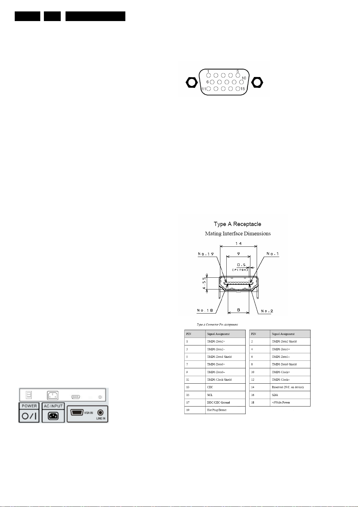
VGA:Video RGB In
Figure 1-2 VGA Connector
1 - Video Red 0.7 VPP / 75 ohm
2 - Video Green 0.7 V
3 - Video Blue 0.7 VPP / 75 ohm
4 – n.c
5 –Ground Gnd
6 -Ground Red Gnd
7 -Ground
en Gnd
Gre
8 -Ground Blue Gnd
9 - +5V_DC +5V
10 -Gnd Sync Gnd
11
- n.c.
12
- DDC_SDA DDC data
- H-sync 0 - 5V
13
14
- V-sync 0 - 5V
15
- DDC_SCL DDC clock
HDMI:
Digital Video In
PP / 75 ohm
DC
Sound
1.1.2
Sound
systems : MTS (NTSC), FM-FM
Internal
speaker : 10 W x 2 stereo, volume adjustable
1.1.3 Miscellaneous
Po
wer supply:
ower voltage (VAC) : 90-264V
-AC P
-AC Power frequency (Hz) : 47~63Hz
Ambient conditions:
-Temp
erature range : 0~35°C
- Maximum humidity : 10%~90%
Po
wer consumption
- Normal operation : 185 W
- Stand
Dimensions
Weight (kg) :19.5Kg
-by: < 2 W
(WxHxD mm) :600*980*252
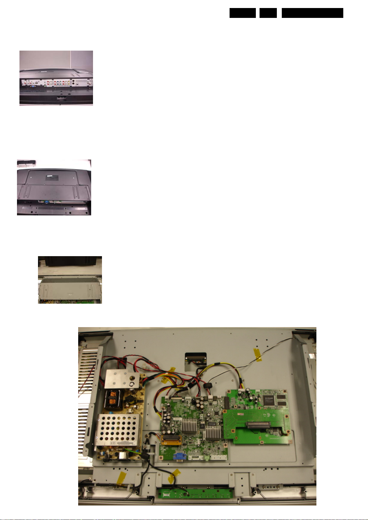
1.2 Connections
1.
2.1 Rear I/O connections
Technical Specifications, Connections, and Chassis Overview
EN 2
1.
MQC2.OA LA
1.2.2 Right I/O Connections
RF_Analog 75ohm Unbalance F-type connector
RF_Digital 75ohm Unbalance F-type connector
AV1-S1/AV2-S2: S-Video 1Fh Y/C-In
1 -Ground Y Gnd
2 -Ground C Gnd
3 -Video Y 1Vpp/75 ohm
4 -Video C 0.3Vpp/75 ohm
AV1/AV2 Video In, Audio In
1 -Audio R 0.5 Vrms/10Kohm
2 -Gnd CVBS Gnd
3 -Video CVBS 1Vpp/75 ohm
4 -Audio L 0.5 Vrms/10Kohm
YPBPR1/YPBPR2
Wh….-Audio L 0.5 Vrms/10Kohm
Rd….-Audio R 0.5 Vrms/10Kohm
Bu Video Pb 0.7 Vpp/75 ohm
Rd Video Pr 0.7 Vpp/75 ohm
Gn Video Y 1Vpp/75 ohm
1.3 Chassis overview
1.2.3 Left I/O Connections
Line-out
1 Audio R 0.5 Vrms/10Kohm
2 Audio L 0.5 Vrms/10Kohm
Line-in
1 Audio R 0.5 Vrms/10Kohm
2 Audio L 0.5 Vrms/10Kohm
HDMI
1 Video coding: RGB 4.4.4,YCbCr 4.2.2,YCbCr 4.4.4
2.Audio format supported(minimum) 2 channel L-PCM
3.Using an IEC 6095 subpacket structure
Sampling rate 32KHz,44.1Khz,48Khz
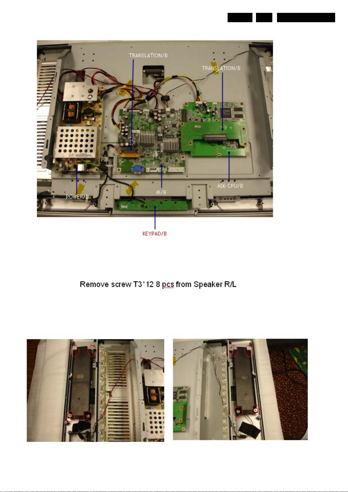
M/B
AD6 CPU/B
Power/B
IR/B
Keypad/B
Translation/BTranslation/B HDMI

EN 3
Safety Instructions, Warnings, and Notes
2.
MQC2.OA LA
2. Safety Instructions, Warnings, and Notes
2.1 Safety Instructions
Safety regulations require that during a repair:
• Connect the set to the AC Power via an isolation
transformer (> 800 VA).
• Replace safety components, indicated by the symbol
only by components identical to the original ones. Any
other component substitution (other than original type) may
increase risk of fire or electrical shock hazard.
Safety regulations require that after a repair, the set must be
returned in its original condition. Pay in particular attention to
the following points:
• Route the wire trees correctly and fix them with the
mounted cable clamps.
• Check the insulation of the AC Power lead for external
damage.
• Check the strain relief of the AC Power cord for proper
function.
• Check the electrical DC resistance between the AC Power
plug and the secondary side (only for sets which have a AC
Power isolated power supply):
1. Unplug the AC Power cord and connect a wire
between the two pins of the AC Power plug.
2. Set the AC Power switch to the "on" position (keep the
AC Power cord unplugged!).
3. Measure the resistance value between the pins of the
AC Power plug and the metal shielding of the tuner or
the aerial connection on the set. The reading should be
between 4.5 Mohm and 12 Mohm.
4. Switch "off" the set, and remove the wire between the
two pins of the AC Power plug.
• Check the cabinet for defects, to avoid touching of any
inner parts by the customer.
,
2.2 Warnings
• All ICs and many other semiconductors are susceptible to
electrostatic discharges (ESD
during repair can reduce life drastically. Make sure that,
during repair, you are connected with the same potential as
the mass of the set by a wristband with resistance. Keep
components and tools also at this same potential. Available
ESD protection equipment:
– Complete kit ESD3 (small tablemat, wristband,
connection box, extension cable and earth cable) 4822
310 10671.
– Wristband tester 4822 344 13999.
• Be careful during measurements in the high voltage
section.
• Never replace modules or other components while the unit
is switched "on".
• When you align the set, use plastic rather than metal tools.
This will prevent any short circuits and the danger of a
circuit becoming unstable.
). Careless handling
2.3 Notes
2.3.1 General
• Measure the voltages and waveforms with regard to the
chassis (= tuner) ground ( ), or hot ground ( ), depending
on the tested area of circuitry. The voltages and waveforms
shown in the diagrams are indicative. Measure them in the
Service Default Mode (see chapter 5) with a color bar
signal and stereo sound (L: 3 kHz, R: 1 kHz unless stated
otherwise) and picture carrier at 475.25 MHz for PAL, or
61.25 MHz for NTSC (channel 3).
• Where necessary, measure the waveforms and voltages
with ( ) and without ( ) aerial signal. Measure the
voltages in the power supply section both in normal
operation ( ) and in stand-by ( ). These values are
indicated by means of the appropriate symbols.
• The semiconductors indicated in the circuit diagram and in
the parts lists, are interchangeable per position with the
semiconductors in the unit, irrespective of the type
indication on these semiconductors.
• Manufactured under license from Dolby Laboratories.
“Dolby” and the “double-D symbol”, are trademarks of
Dolby Laboratories.
2.3.2 Schematic Notes
• All resistor values are in ohms and the value multiplier is
often used to indicate the decimal point location (e.g. 2K2
indicates 2.2 Kohm).
• Resistor values with no multiplier may be indicated with
either an "E" or an "R" (e.g. 220E or 220R indicates 220
ohm).
• All capacitor values are given in micro-farads (µ= x10
nano-farads (n= x10
• Capacitor values may also use the value multiplier as the
decimal point indication (e.g. 2p2 indicates 2.2 pF).
• An "asterisk" (*) indicates component usage varies. Refer
to the diversity tables for the correct values.
• The correct component values are listed in the Electrical
Replacement Parts List. Therefore, always check this list
when there is any doubt.
2.3.3 Rework on BGA (Ball Grid Array) ICs
General
Although (LF)BGA assembly yields are very high, there may
still be a requirement for component rework. By rework, we
mean the process of removing the component from the PWB
and replacing it with a new component. If an (LF)BGA is
removed from a PWB, the solder balls of the component are
deformed drastically so the removed (LF)BGA has to be
discarded.
Device Removal
As is the case with any component that, it is essential when
removing an (LF)BGA, the board, tracks, solder lands, or
surrounding components are not damaged. To remove an
(LF)BGA, the board must be uniformly heated to a temperature
close to the reflow soldering temperature. A uniform
temperature reduces the chance of warping the PWB.
To do this, we recommend that the board is heated until it is
certain that all the joints are molten. Then carefully pull the
component off the board with a vacuum nozzle. For the
appropriate temperature profiles, see the IC data sheet.
Area Preparation
When the component has been removed, the vacant IC area
must be cleaned before replacing the (LF)BGA.
Removing an IC often leaves varying amounts of solder on the
mounting lands. This excessive solder can be removed with
either a solder sucker or solder wick. The remaining flux can be
removed with a brush and cleaning agent.
After the board is properly cleaned and inspected, apply flux on
the solder lands and on the connection balls of the (LF)BGA.
Note: Do not apply solder paste, as this has shown to result in
problems during re-soldering.
-9
), or pico-farads (p= x10
-6
-12
),
).
Directions for Use
Device Replacement
The last step in the repair process is to solder the new
component on the board. Ideally, the (LF)BGA should be
aligned under a microscope or magnifying glass. If this is not
possible, try to align the (LF)BGA with any board markers.
To reflow the solder, apply a temperature profile according to
the IC data sheet. So as not to damage neighboring
components, it may be necessary to reduce some
temperatures and times.
More Information
For more information on how to handle BGA devices, visit this
URL: www.atyourservice.ce.philips.com
not available for all regions). After login, select “Magazine”,
then go to “Workshop Information”. Here you will find
Information on how to deal with BGA-ICs.
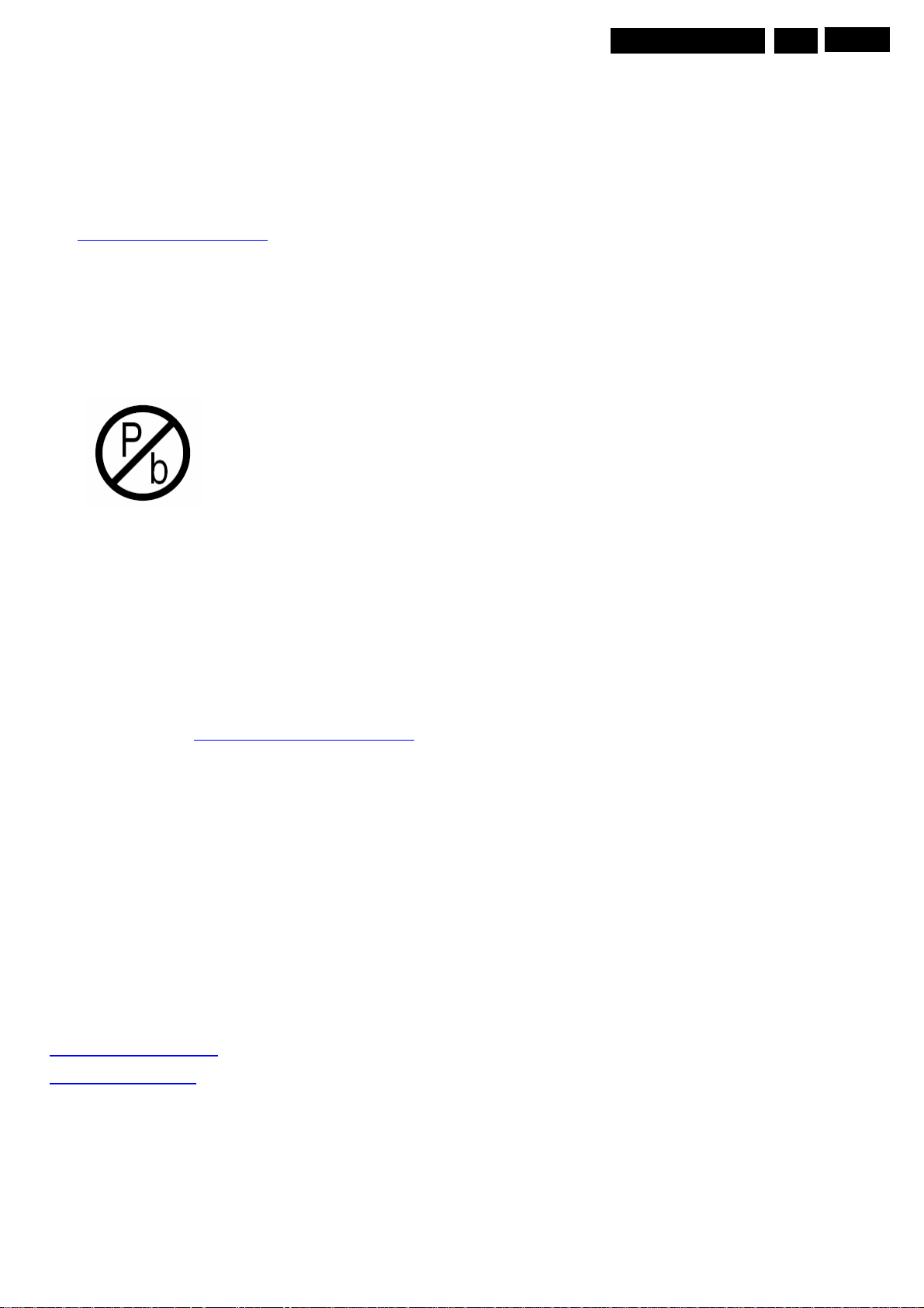
2.3.4 Lead Free Solder
Philips CE is going to produce lead-free sets (PBF) from
1.1.2005 onwards.
Lead-free sets will be indicated by the PHILIPS-lead-free logo
on the Printed Wiring Boards (PWB):
Figure 2-1 Lead-free logo
This sign normally has a diameter of 6 mm, but if there is less
space on a board also 3 mm is possible.
In case of doubt wether the board is lead-free or not (or with
mixed technologies), you can use the following method:
• Always use the highest temperature to solder, when using
SAC305 (see also instructions below).
• De-solder thoroughly (clean solder joints to avoid mix of
two alloys).
Caution: For BGA-ICs, you must use the correct temperature
profile,which is coupled to the 12NC. For an overview of these
profiles, visit the website http://www.atyourservice.ce.philips.com/
You will find this and more technical information within the
"Magazine", chapter "Workshop information".
For additional questions please contact your local repair-helpdesk.
(needs subscription,
Due to lead-free technology some rules have to be respected
by the workshop during a repair:
• Use only lead-free soldering tin Philips SAC305 with order
code 0622 149 00106. If lead-free solder paste is required,
please contact the manufacturer of your soldering
equipment. In general, use of solder paste within
workshops should be avoided because paste is not easy to
store and to handle.
• Use only adequate solder tools applicable for lead-free
soldering tin. The solder tool must be able
– To reach at least a solder-tip temperature of 400°C.
– To stabilise the adjusted temperature at the solder-tip.
– To exchange solder-tips for different applications.
• Adjust your solder tool so that a temperature around 360°C
-380°C is reached and stabilised at the solder joint.
Heating time of the solder-joint should not exceed ~ 4 sec.
Avoid temperatures above 400°C, otherwise wear-out of
tips will rise drastically and flux-fluid will be destroyed. To
avoid wear-out of tips, switch “off” unused equipment or
reduce heat.
• Mix of lead-free soldering tin/parts with leaded soldering
tin/parts is possible but PHILIPS recommends strongly to
avoid mixed regimes. If not to avoid, clean carefully the
solder-joint from old tin and re-solder with new tin.
• Use only original spare-parts listed in the Service-Manuals.
Not listed standard material (commodities) has to be
purchased at external companies.
• Special information for lead-free BGA ICs: these ICs will be
delivered in so-called "dry-packaging" to protect the IC
against moisture. This packaging may only be opened
short before it is used (soldered). Otherwise the body of the
IC gets "wet" inside and during the heating time the
structure of the IC will be destroyed due to high (steam)pressure inside the body. If the packaging was opened
before usage, the IC has to be heated up for some hours
(around 90°C) for drying (think of ESD-protection !).
Do not re-use BGAs at all!
• For sets produced before 1.1.2005, containing leaded
soldering tin and components, all needed spare parts will
be available till the end of the service period. For the repair
of such sets nothing changes.
2.3.5 Practical Service Precautions
• It makes sense to avoid exposure to electrical shock.
While some sources are expected to have a possible
dangerous impact, others of quite high potential are of
limited current and are sometimes held in less regard.
• Always respect voltages. While some may not be
dangerous in themselves, they can cause unexpected
reactions - reactions that are best avoided. Before reaching
into a powered TV set, it is best to test the high voltage
insulation. It is easy to do, and is a good service precaution.
MQC2.OA LA
3.
EN 4
3. Directions for Use
You can download this information from the following websites:
http://www.philips.com/support
http://www.p4c.philips.com
Mechanical Instructions
EN 5
4.
MQC2.OA LA
4. Mechanical Instructions
Index of this chapter:
4.1 Cable Dressing
4.2 Foam Bars
4.3 Panel/PCBA Removal
4.4 Disassemblyt and Re-assembly
4.1 Cable Dressing
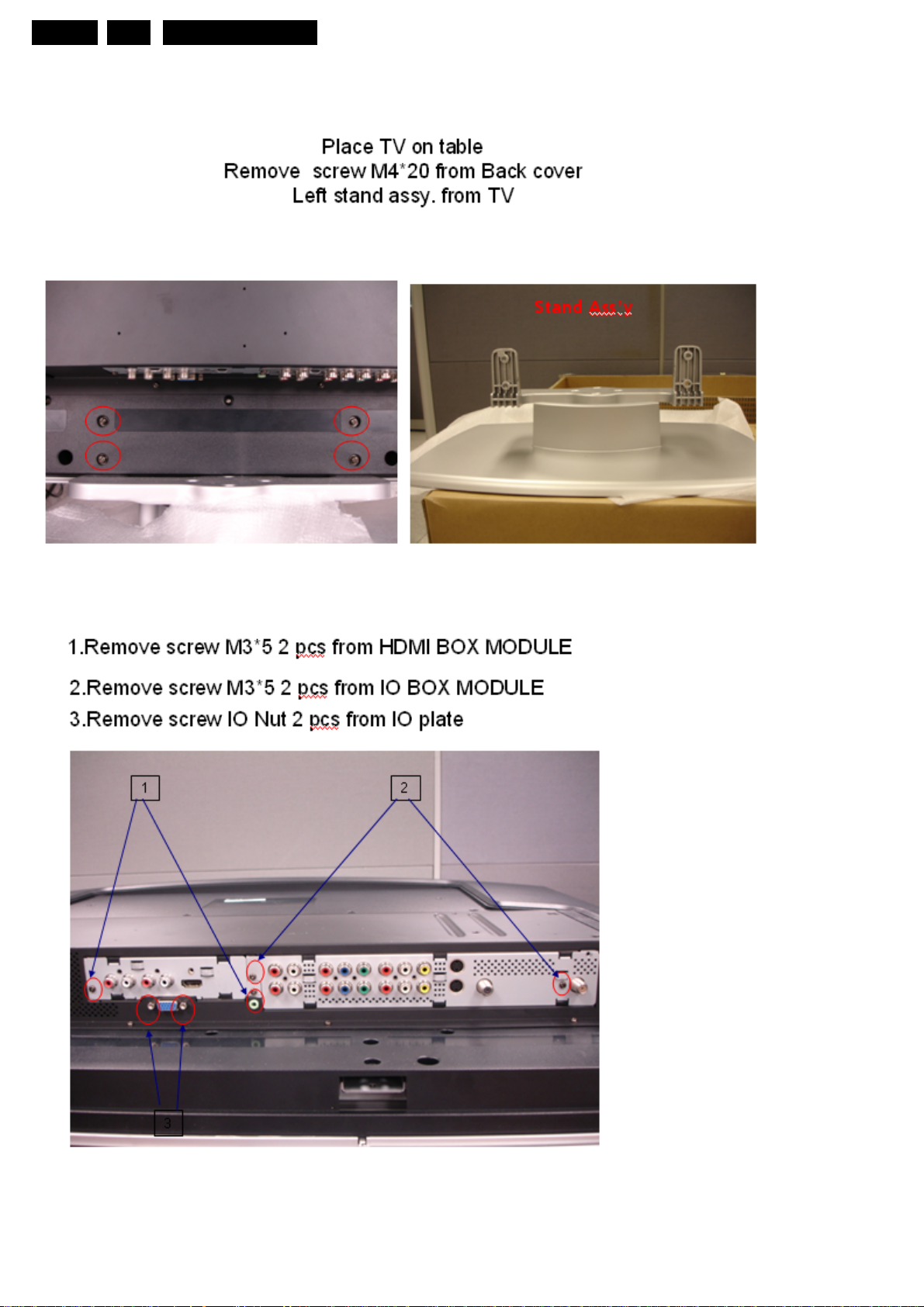
4.2 Service Positions
4.2.2 Stands
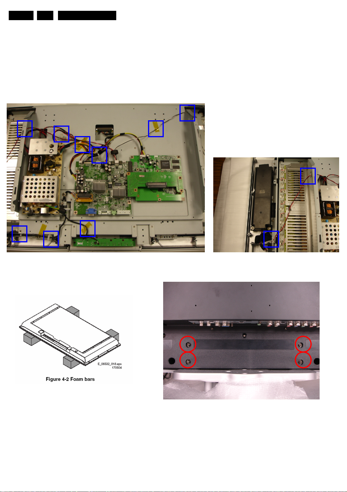
4.2.1 Foam Bars
The foam bars (order code 3122 785 90580 for two pieces) can
be used for all types and sizes of Flat TVs. By laying the TV
face down on the (ESD protective) foam bars, a stable situation
is created to perform measurements and alignments.
By placing a mirror under the TV, you can monitor the screen.
The stands can be mounted with the back cover removed or
still left on. So, the stand can be used to store products or to do
measurements. It is also very suitable to perform duration tests
without taking much space, without having the risk of overheating
,or the risk of products falling. The stands can be mounted and
removed quick and easy with use of the delivered screws that
can be tightened and loosened manually without the use of tools.
See figure above.
Note: Only use the delivered screws to mount the monitor to
the stands
Figure 4-3 Stands
Mechanical Instructions
4.3 Panel/PCBA removal
4.3.1 IO/Sub IO
Warning: Disconnect the AC Power cord before you open the
set.
1. Place the TV set upside down on a table top, using the
foam bars (see part "Foam Bars").
Caution: do not put pressure on the display, but let the
monitor lean on the speakers or the Front cover.
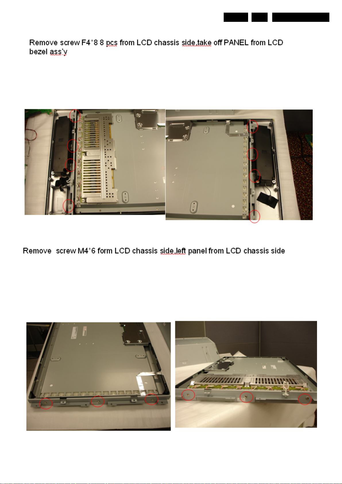
2. Remove M3*5(4 pieces) from Left/Right I/O Box of rear side.
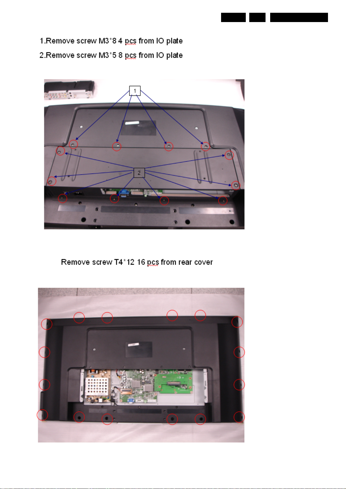
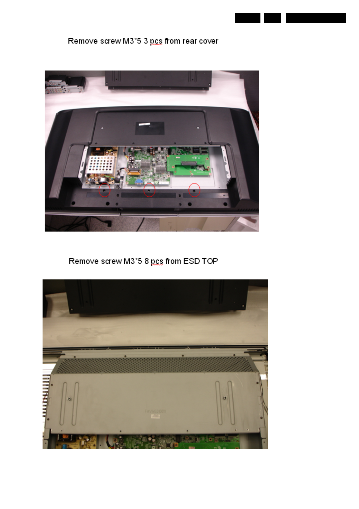
4.3.2 I/O plate/Back cover/ R&L Speaker
2. Remove screw T4*12 16pcs,M3*5 3 pcs from the Back cover.
. 3. Lift the back cover from the set. Make sure that wires and
4. Remove screw T3*12 8 pcs from L/R speaker
1.. Remove screw M3*8 4pcs,M3*5 8 pcs and I/O nut*2 from I/O plate.
flat foils are not damaged during the back cover removal.
4.3.3 ESD TOP
EN 6
4.
MQC2.OA LA
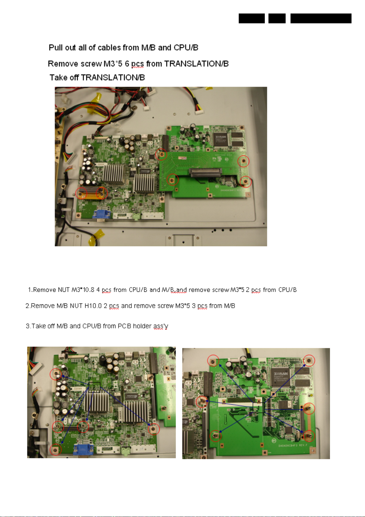
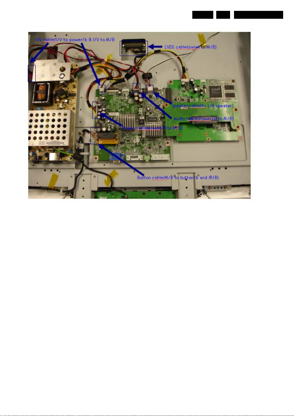
4.3.4 Main Board & Translation Board
1. Disconnect all cable from Base unit
2. Remove the fixation screws
3. Take out the Translation/B & Main Board
4.3.5 AD6 CPU Board & Translation Board
1. Remove the fixation screws
2. Take out the Ttanslation/B & Main Board
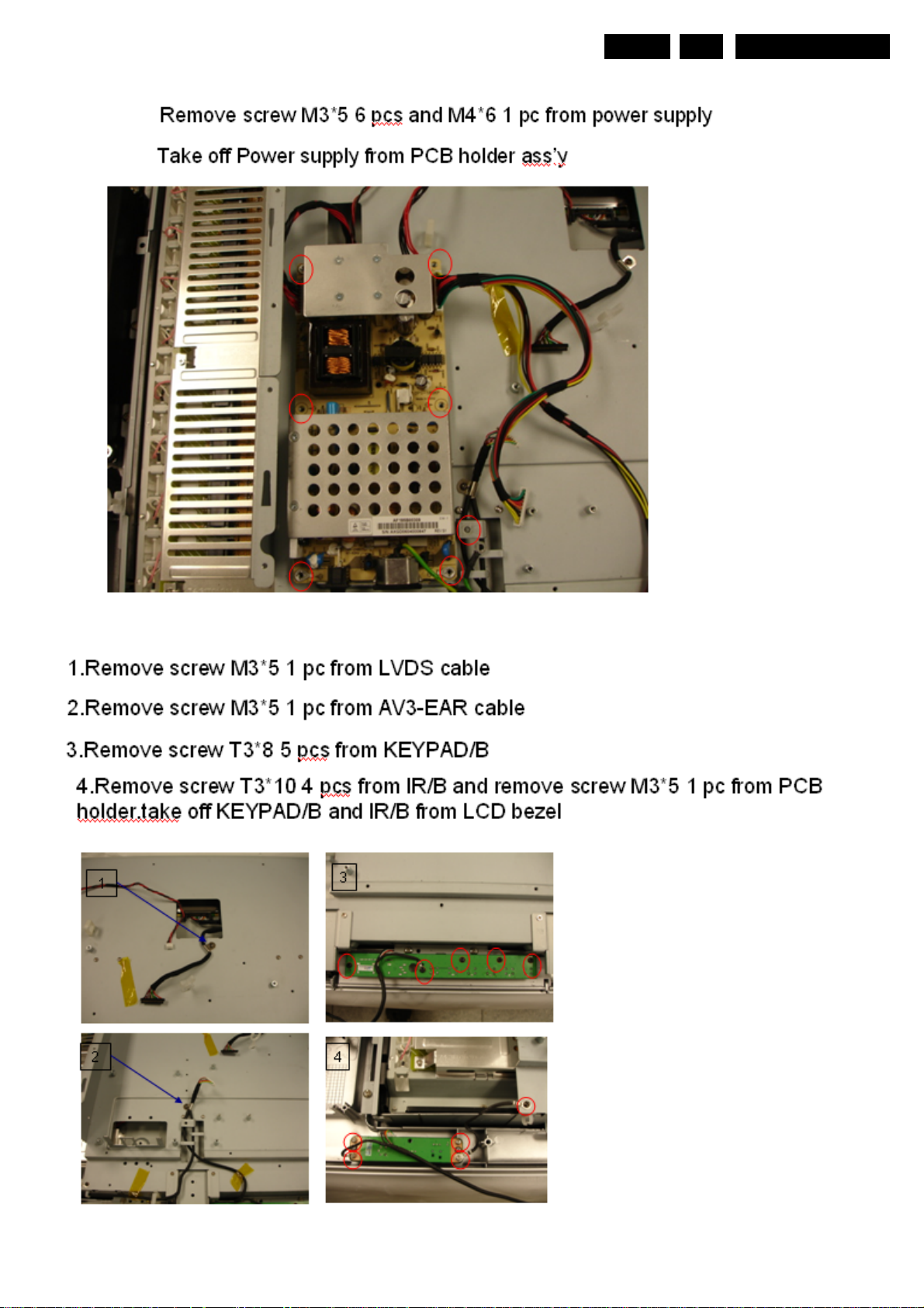
4.3.6 Power Board
1. Remove the fixation screws
2. Take out the Power/B.
4.3.7 Button Board
1. Remove the fixation screws
2. Take out Button/B.
4.3.8 IR Board
1. Remove the fixation screws
2. Take out IR/B.
4.3.9 LCD Panel
1. Remove the fixation screws from
PCB-Holder ass’y
2. Take out PCB-Holder ass’y
3. Remove the fixation screws from LCD
chassis
4. Lift the panel from LCD bezel
1. Remove screw M3*5 8pcs from ESD TOP.
2. Lift the ESD TOP from chassis.
EN 7
Mechanical Instructions
4.
MQC2.OA LA
Disassembly process
4.4.1
4.4.2
Mechanical Instructions
EN 8
4.
MQC2.OA LA
4.4.3
4.4.4
Mechanical Instructions
4.4.5
EN 9
4.
MQC2.OA LA
4.4.6
Mechanical Instructions
4.4.7
EN 10
4.
MQC2.OA LA
4.4.8
Mechanical Instructions
4.4.9
EN 11
4.
MQC2.OA LA
4.4.10
Mechanical Instructions
4.4.11
EN 12
4.
MQC2.OA LA
4.4.12
Mechanical Instructions
4.4.13
EN 13
4.
MQC2.OA LA
4.4.14
Mechanical Instructions
4.4.15
EN 14
4.
MQC2.OA LA
4.4.16
Mechanical Instructions
4.4.17
EN 15
4.
MQC2.OA LA
4.4.18 Re-assembly
To re-assemble the LCD panel, execute all processes
in reverse order.
Note:
.While re-assemble, make sure that all are placed and
And connected in their original position. See figure
“Cable dressing”
.Pay special attention not to damage the EMC foams at the
SSB shielding. Check that EMC foams are put correctly on
their places.
Service mode, Fault Finding
5 Service mode and Fault Finding
Index if this chapter:
5.1 Service Modes for ATV
5.2 Service Modes for DTV
5.3 Fault Finding
5.1 Service Mode (update ATV BIOS)
Purpose
. To update new version ATV BIOS
Tools
. ISP Board
. RS232 cable
. VGA cable
. Software (Pixlworks)
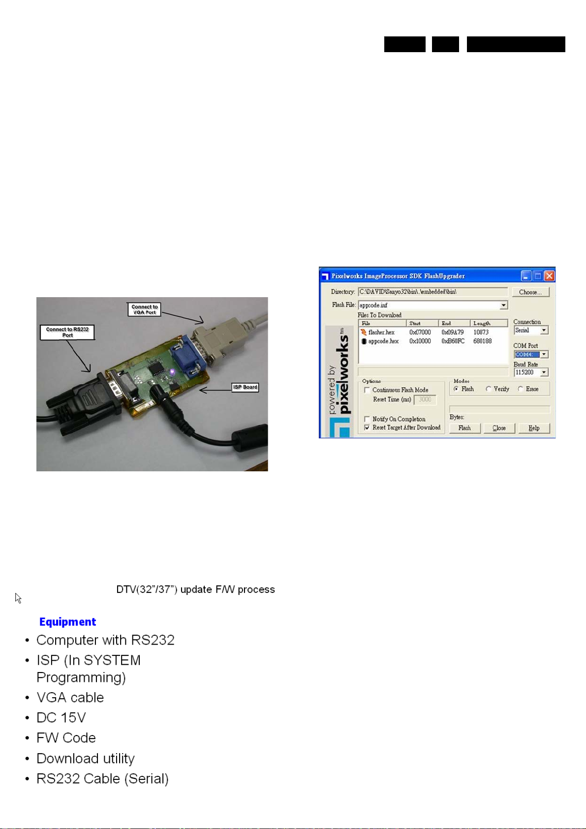
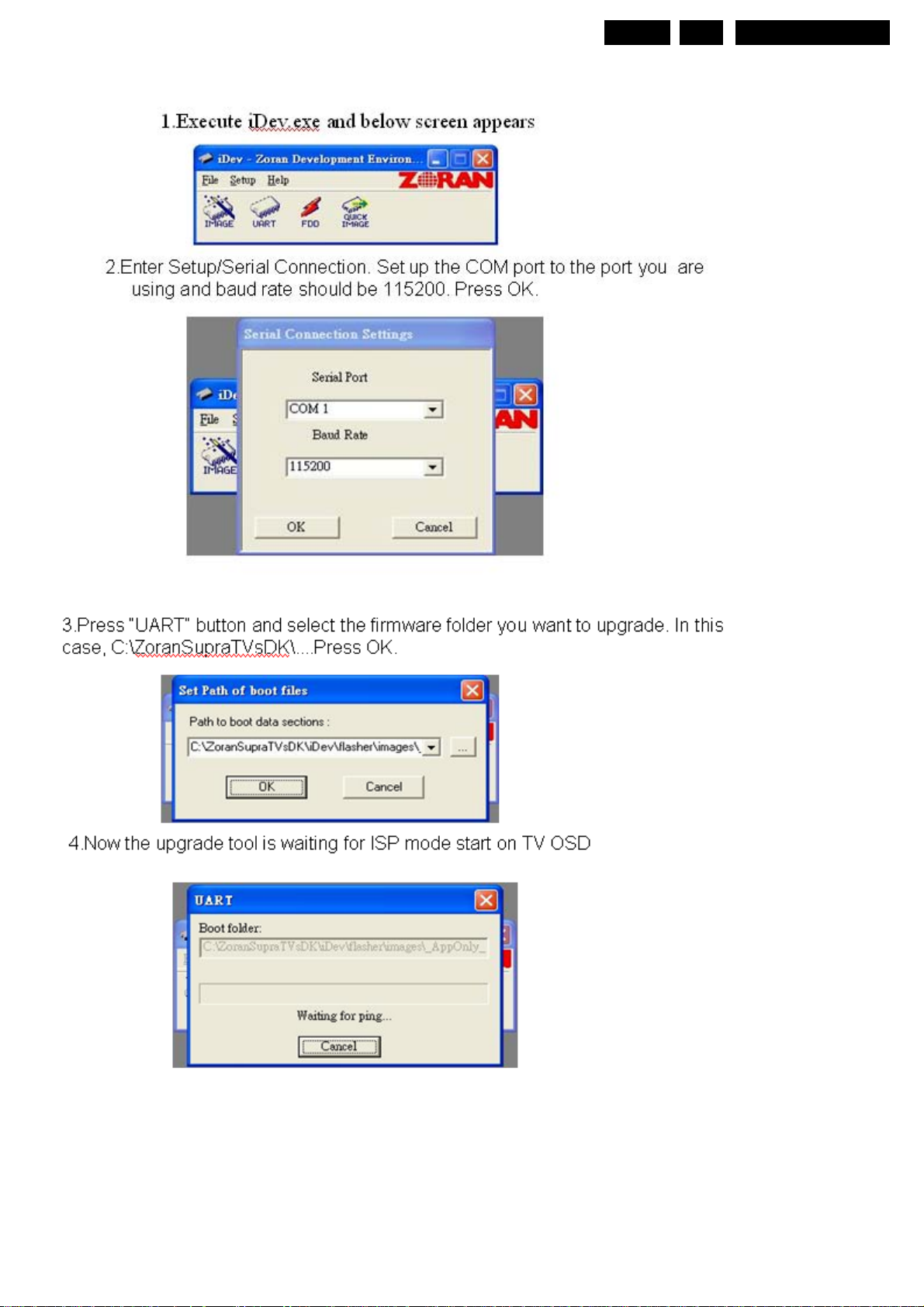
5.2 Service Mode (update DTV BIOS)
Purpose
. To update new vers ion DTV BIOS
Tools
EN 16
5
MQC2.OA LA
Setup
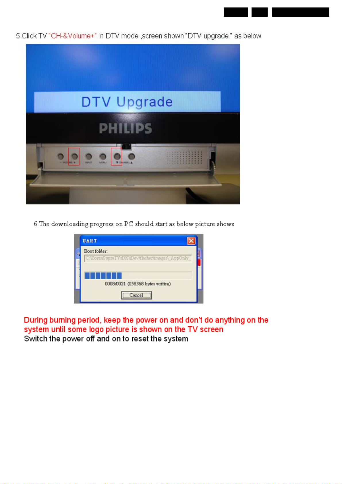
1. Off TV Pow e r
2. Process Pixlworks program
3. Choose appcode.inf
4. Check connection. Should be in serial
5. Check COM Port of R232
6. Check Baud Rate
7. Click Flash
8. Turn on the TV .The program will automatic
9. After few seconds, then screen will showing flash
completed. TV will power on itself
Service mode, Fault Finding
Setup
EN 17
5
MQC2.OA LA
Service mode, Fault Finding
EN 18
5
MQC2.OA LA
Service mode, Fault Finding
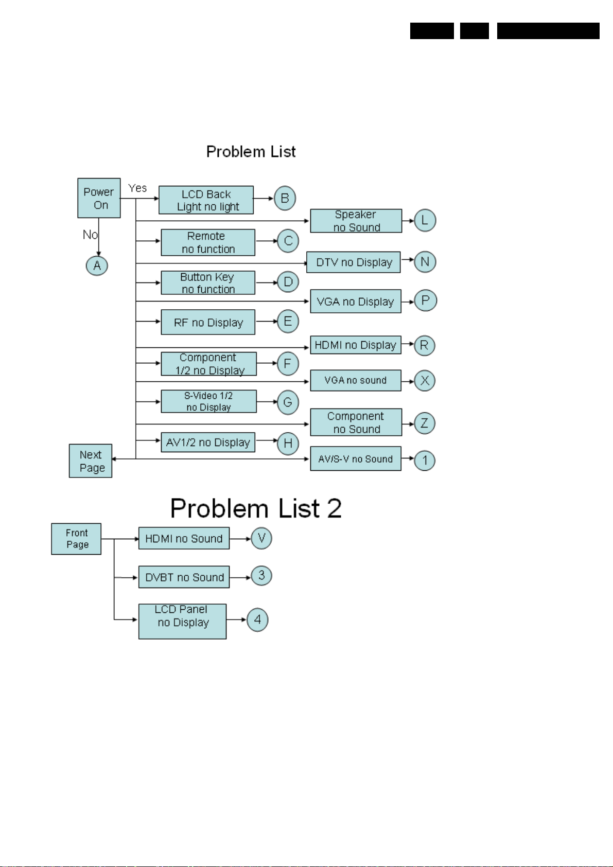
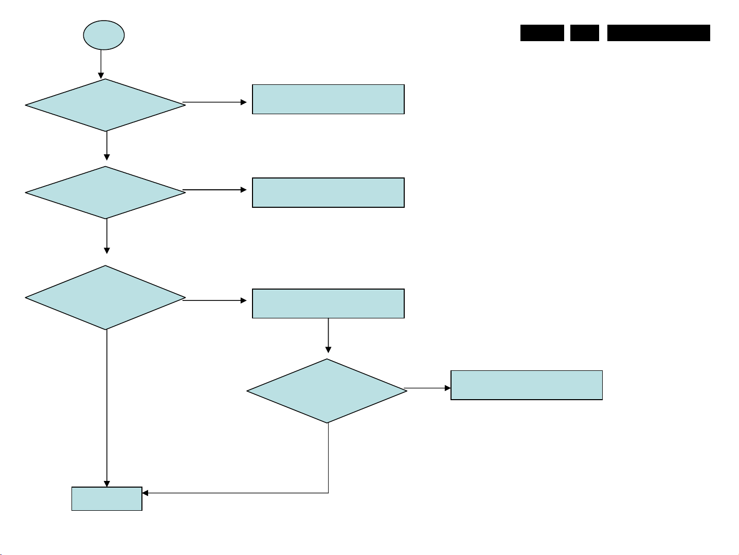
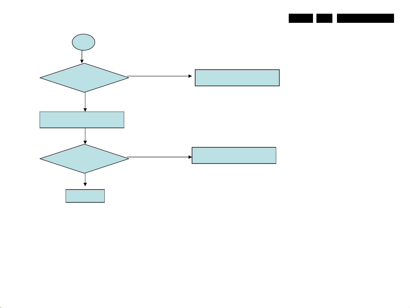
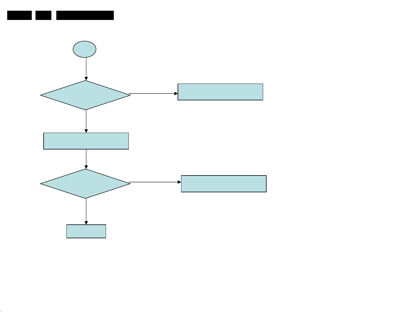
5.3 Fault Finding
Purpose
To find the fault
How to find fault
EN 19
5
MQC2.OA LA
A
Service mode, Fault Finding
EN 20
5
MQC2.OA LA
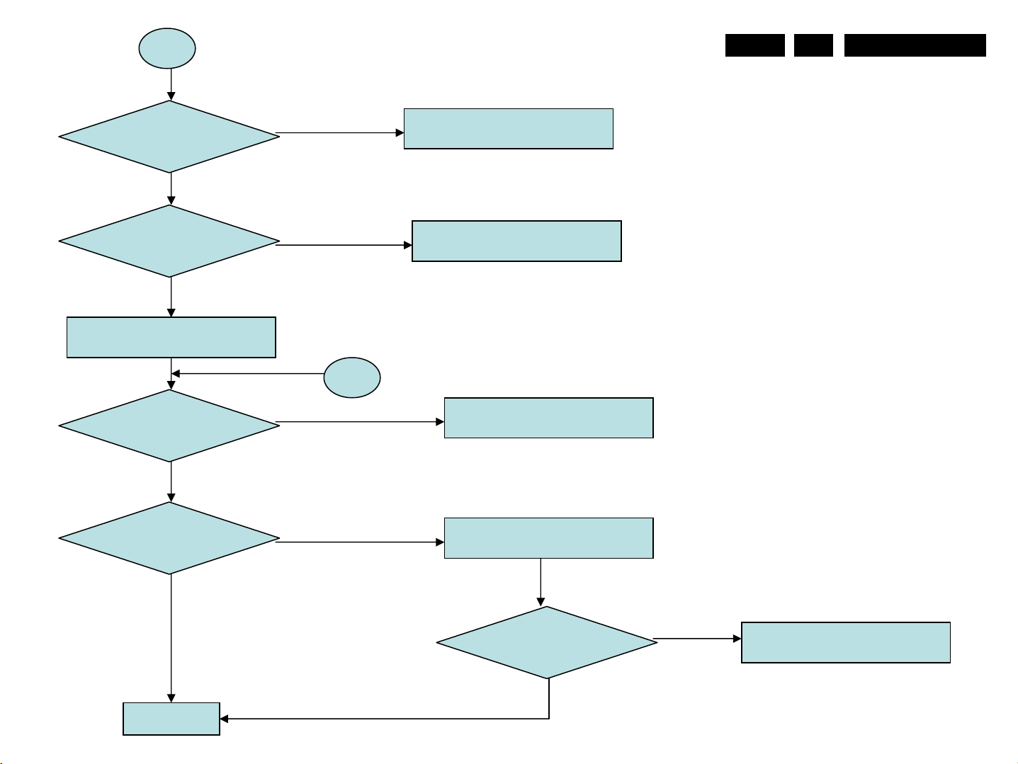
Power cable
Plug-in?
LED bright?
LCD panel can
Display?
TV source can
Display?
Check Power cable
Replace P/B or P/B to M/B
Power cable
Replace M/B
LCD panel can
Display?
Replace I/O board
Replace I/V to power cable
or LVDS cable
Speaker have sound
Output?
TV source can
Display?
Replace Audio/B Audio/B or I/O
Audio/B cable
Replace Tuner/B
EN 21
5
MQC2.OA LA
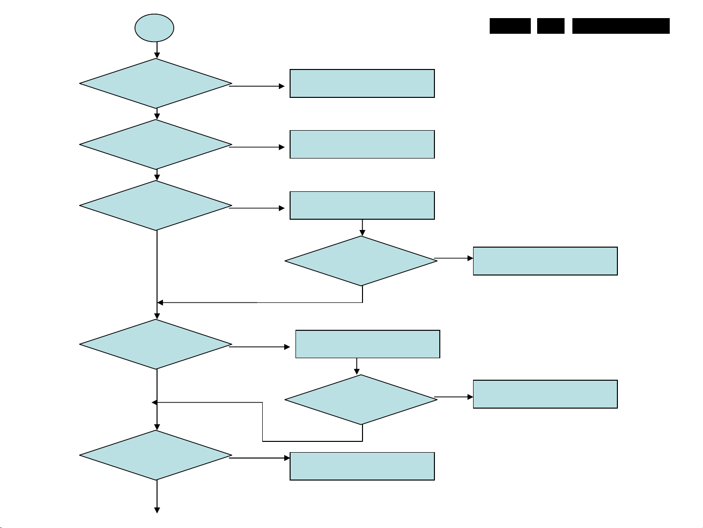
Service mode, Fault Finding
DVBT/ATSC source
can display
END
B
Inverter power cable
Plug in?
LCD back light
Bright?
Replace DVBT/ATSC board
Change inverter power cab le
Replace Power board
LCD back light
Bright?
END
Replace LCD Inverter boa rd
LCD back light
Bright?
Replace M/B
C
Service mode, Fault Finding
EN 22
5
MQC2.OA LA
Remote control have
Battery?
IR board cable
Plug in?
Press remote menu key
OSD can display?
Change battery
Check IR/B cable or replace
IR/B cable
Replace IR/B
Press remote menu key
OSD can display?
Replace M/B
END
EN 23
5
MQC2.OA LA
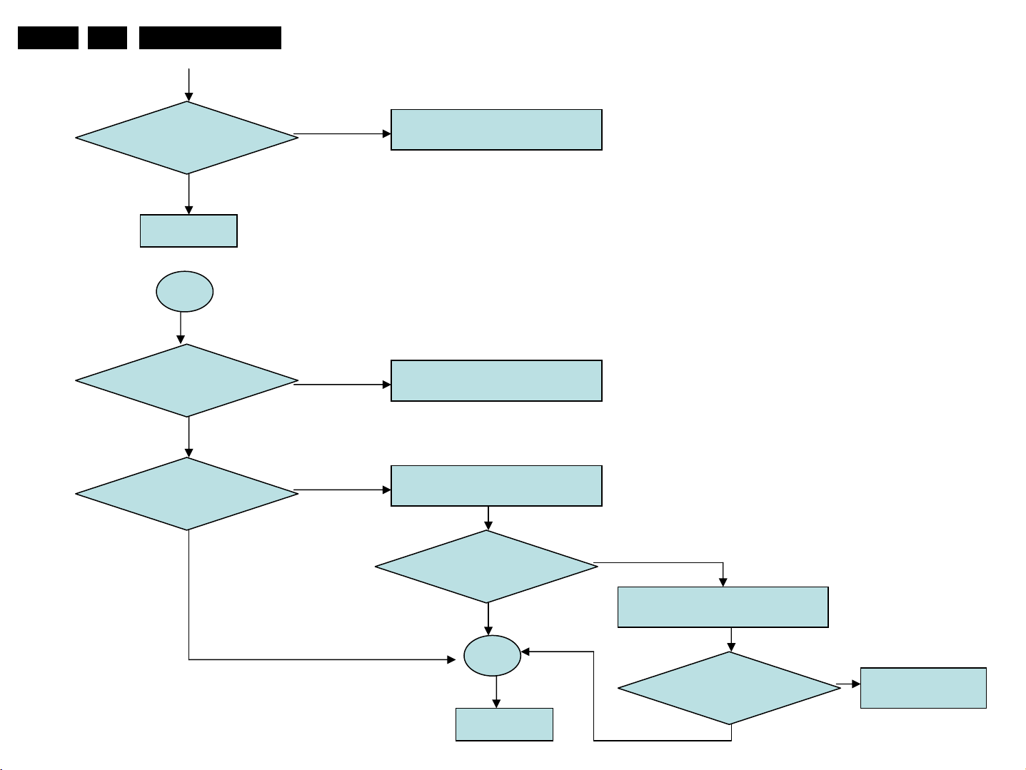
D
Service mode, Fault Finding
Key board cable
plug in
Press Menu key
Check function?
Check K/B cable or replace
K/B cable
Replace K/B cable
Press Menu key
Check function?
Replace K/B cable
ENDEND
Service mode, Fault Finding
E
EN 24
5
MQC2.OA LA
RF cable
Plug in?
CVBS1 can’t
display
Replace I/O board
RF can display
Check RF cable or replace
RF cable
Replace Tuner board
Replace M/B
Replace I/O board
END
EN 25
5
MQC2.OA LA
F
Service mode, Fault Finding
Component cable
Plug in?
Replace I/O board
Component can
Display?
END
Check component cable or
Replace component cable
Replace M/B
Service mode, Fault Finding
G
EN 26
5
MQC2.OA LA
S-video cable
Plug in?
Replace I/O board
S-video can
display
END
Check S-video cable or replace
S-video cable
Replace M/B
EN 27
5
MQC2.OA LA
H
Service mode, Fault Finding
CVBS cable
Plug in?
Replace I/O board
CVBS can
display
END
Check CVBS cable or replace
CVBS cable
Replace M/B
L
Service mode, Fault Finding
EN 28
5
MQC2.OA LA
Audio R/L cable
Plug in?
Video can display?
Mute turn-off,volume=30
Earphone remove
Speaker R/L cable
Plug in?
Speaker have sound
output
Check Audio R/L cable or
Replace Audio R/L cabl e
Check video cable or replace
Video cable
L1
Check speaker cable or replace
Speaker cable
Replace I/O to Audio/B cable
And Audio/B
END
Speaker have sound
output
Replace I/O board

EN 29
5
MQC2.OA LA
N
Service mode, Fault Finding
Check DVBT/ATSC power
Cable plug in?
Replace DVBT/ATSC board
DVBT/ATSC can display
END
Check or replace DVBT/ATSC
Power cable
Replace M/B

P
VGA cable plug in?
Read EDID data
Service mode, Fault Finding
Check VGA cable or replace
VGA cable
EN 30
5
MQC2.OA LA
EDID data normal?
VGA can display?
END
Write EDID data
Replace M/B

EN 31
5
MQC2.OA LA
R
Service mode, Fault Finding
HDMI cable plug in?
Read EDID data
EDID data normal?
HDMI can display?
END
Check HDMI cable or replace
HDMI cable
Write EDID data
Replace M/B

V
HDMI cable plug in?
Read EDID data
Service mode, Fault Finding
Check HDMI cable or replace
HDMI cable
EN 32
5
MQC2.OA LA
EDID data normal?
Mute turn-off,Volume – 30
Earphone remove
PC volume setting to On
HDMI can display?
HDMI sound normal?
Write EDID data
Check HDMI cable or DVD player
Or replace HDMI cable
Replace M/B
HDMI sound normal?
Replace I/O board
HDMI sound normal?
L1
END

EN 33
5
MQC2.OA LA
X
Service mode, Fault Finding
Line in cable plug in?
Mute turn-off,Volume – 30
Earphone remove
PC volume setting to On
PC/DVI can display?
PC/DVI sound normal?
Check line in cable or repla c e
Line in cable
Check Video cable or PC or
Replace VGA/DVI cable
Replace M/B
Replace I/O board
PC/DVI sound normal?
END
PC/DVI sound normal?
L1

Z
Service mode, Fault Finding
EN 34
5
MQC2.OA LA
Component cable
Plug in?
Mute turn-off,Volume – 30
Earphone remove
Component source
Can display?
Component sound
Normal?
Check component cable
Or replace component cable
Check component cable
Or replace component cable
Replace I/O board
Component sound
Normal?
END
L1

EN 35
5
MQC2.OA LA
1
Service mode, Fault Finding
AV1/S-video/R-L
Cable plug in?
Mute turn-off,Volume – 30
Earphone remove
AV1/S-video source
Can display?
AV1/S-video sound
normal?
Check video and R-L cable or
Replace video or R-L cable
Check video and R-L cable or
Replace video or R-L cable
Replace I/O board
AV1/S-video sound
normal?
L1
END

3
Service mode, Fault Finding
EN 36
5
MQC2.OA LA
DVBT/ATSC RF cable
Plug in?
Mute turn-off,Volume – 30
Earphone remove
DVBT/ATSC source
Can display?
DVBT/ATSC sound
normal?
Check RF cable or replace RF
cable
N
Replace D-Tuner/B
DVBT/ATSC sound
normal?
Replace DVBT/ATSC
M/B
END
DVBT/ATSC sound
normal?
Replace M/B
DVBT/ATSC sound
normal?
L1

EN 37
5
MQC2.OA LA
4
Service mode, Fault Finding
Check M/B to LCD panel
LVDS cable plug in?
Check LCD panel
Tcon board voltage
Check LCD panel
backlight
Replace M/B
LCD panel display
Normal?
Check LVDS cable or replace
LVDS cable
Replace LVDS cable
B
Replace LVDS cable
END
Replace LCD panel
END

EN 38
6
MQC2.OA LA
6. Block Diagrams
Wiring Diagram
Block Diagrams

Main Board Block diagrams
Block Diagrams
EN 39
6
MQC2.OA LA

EN 40
6
MQC2.OA LA
Io Board Block diagrams
Block Diagrams

Digital TV system Block Diagrams
Block Diagrams
EN 41
6
MQC2.OA LA

EN 42
7. Circuit Diagrams ,PCBA Layouts
MB
7
MQC2.OA LA
Circuit Diagrams
PW328 + PW3300B + PW9701 + HDMI CKT.
PAGE TITLE
01. TITLE P AGE
02. BLOCK DIAGRAM
03. VGA INPUT
04. HDMI INPUT
05. HDMI
06. DVI INPUT
07. PW3300 INPUT
08. PW3300 POWER
09. I 2S BUS
10. PW328 Scaler
11. PW328 DDR
12. PW328 Flash
13. PW328 IO
14. PW328 POWER
15. PW328 REGULAR
16. MISC
17. AUDIO AMP
18. SOUND DE CODER
19. PIXELAMP PW9700
20. LVDS OUT
21. IO CONNECTOR
22 . DC DC
23. REVESION
Title
<Title>
Size Document Number Rev
<Doc> <RevCode>
A
Date: Sheet
of
123Monday, April 10, 2006

EN 43
7
MQC2.OA LA
HEAD PHONE
AUDIO AMP
R/L
FOR 3D OPTION
RGB 24bit O
RGB 24bit E
4052
Audio
SW
RGB HV
HD_Y.PB.PR
R/L
16M
FLASH MEMORY
SCALER
IN0
IN1
MUXIN1
I2S1
AI3
PIXEL AMP
R..G.B DATA
LVDS
PANEL/
Backlight/
POWER
Control
Watchdog
LVDS
option
12V/5V
26"/32"
LCD Panel
AV4_IN_OUT
SCART R.G.B
AV1
AV2
AV3
S-VIDEO1
DVI CONNECTOR
VGA CONNECTOR
DVBT BOARD
DDC
HDMI CONNECTOR
Y.PB.PR CONNECT
R/L
SPDIF
TMDS
SPDIF
PC LINE IN
CONNECTOR
DDC
DDC
TMDS
YPbPr
HDMI
Receiver
R/L
R/L
R/L
SDRAM
1MX16
AD4
AD3
AD2
RX/0/1/2
Video Decoder
AD1
RGB 24bit E
I2S
DAC
R/L
AUDIO
DELAY
I2S
R
MSG3415
L
SCART R/L
SCART OUTPUTR/L
Y.CB.CR
AV1
AV2
AV3
S-Video1
AV4_IN_OUT
IR/KB/LED
EEPROM
256M DDR
I2C
MUXIN3
RXD/TXD
UART
Control
PROJECT : NEW-32
Title
Size Document Number Rev
C
Date: Sheet
Quanta Computer Inc.
BLOCK
I/O
223Monday, April 10, 2006
of
B

EN 44
7
MQC2.OA LA
VGA_IN
GSDA
GSCL
1 2
C19
22p3
1 2
1 2
C15
22p3
C20
22p3
1 2
GSCL
GSDA
C11
22p3
D8
5.6V
5VS
21
21
D2
BAV99W
3
D4
1N4148
C14
22p3
1 2
C17
0.1u3
1 2
8
VCC
7
WP
6
SCL
5
SDA
24LC02A
R21
357R3
21
D3
BAV99W
3
FB1 BEAD/3
1 2
FB2 BEAD/3
1 2
FB3 BEAD/3
1 2
VGA_DDC_VCC
U2
1
A0
2
A1
3
A2
4
VSS
RXD_A
100R3
R4
RXD_A 22
1 2
1 2
1 2
C3
NC10p3
C6
NC10p3
C9
NC10p3
R17
10K3
MMBT3904L
Q1
1 3
C1 0R5
C4 0R5
C7 0R5
R20
2
2K3
VGA_R 9
VGA_G 9
VGA_B 9
VGA_DET 12
R5 M600/3
R8
10K3
R11 M600/3
R13
10K3
EDID_PROTECT 4,5,12
TXD12
TXD_LPC22
RXD12
RXD_LPC22
1 2
U1A
74LCX14
11 10
U1E
74LCX14
V33
R580
47K3
R641
1M3
D38
3.3V
R581
47K3
12
14
15
11
C568
0.1u3
R643 100
R586
470K3
D1
BAV99W
3
1617
CON1
2 3
2 3
D9
5.6V
2 3
D5
5.6V
D6
5.6V
R7 100R3
R10 100R3
5VS
1
R1
C10
22p3
75R3F
R2
75R3F
R3
75R3F
C2
1 2
NC/10P3
C5
1 2
NC/10P3
C8
1 2
NC/10P3
C12
22p3
1 2
6
2
7
3
8
4
9
5
10
PC_5V
1 2
D7
DAN202U
3
1 2
R16
R15
3.3K3
3.3K3
R18 100R3
R19 100R3
11
12
13
14
15
2 3
A0
A1
A2
A3
1
B0
GND
5
B1
2
B2
4
B3
74HCT4052
U36
3 4
U1B
74LCX14
9 8
U1D
74LCX14
5 6
VEE
16
VDD
An
Bn
S1
S0
U1C
5VS
12
C567
0.1u3
13
3
7
6
E
8
9
10
R639
10K3
74LCX14
R637 100
R638 100
R640
10K3
R6 NC3
R9 75R3F
R12 NC3
R14 75R3F
V33
R642
100k
D39 1N4148
R587
220k
UART_SW1 12,22
UART_SW0 12,22
C13
22p3
C16
22p3
V33
C18 0.1u3
147
13 12
U1F
74LCX14
C569
1u5
TXD_A
RXD_A
VGA_VS 9,12
VGA_HS 9,12
R585
0R3F
VGA_WEAK_UP 12,22
0825
357R3
R23
TXD_A
TXD_A 22
PROJECT : NEW- 32
Quanta Com puter Inc.
Title
Size Docum ent N um ber Rev
Custom
Date: Sheet
I/O
VGA-INPUT
of
323Monday, April 10, 2006
B
C
5VSS
CONN_60P
59 60
57 58
55 56
SCL5,8,12,22
HS1
R835
HS1
IN0B2
IN0B4
IN0B6
IN0B8
IN0G2
IN0G4
IN0G6
IN0G8
IN0R2
IN0R4
IN0R6
IN0R8
0R
HDMI_L17
CE_REMOTE12
HDMI_SW112
EDID_PROTECT3,5,12
SCDT12
IN0HS6,9
IN0CLK6,9
53 54
51 52
49 50
47 48
45 46
43 44
41 42
39 40
37 38
35 36
33 34
31 32
29 30
27 28
25 26
23 24
21 22
19 20
17 18
15 16
13 14
11 12
9 10
7 8
5 6
3 4
1 2
GND GND
J4
SCREW H OLE
HDMI_SPDIF
H5
IN0B3
IN0B5
IN0B7
IN0B9
IN0G3
IN0G5
IN0G7
IN0G9
IN0R3
IN0R5
IN0R7
IN0R9
RCA_AU_ROUT 17RCA_AU_LOUT17
SDA 5,8,12,22
AUDIO_SW5 12
HDMI_R 17
TP105
HDMI_SW0 12
HDMI_RESETn 12
RX_INT# 11
IN0VS 6,9
IN0PEN 6,9
IN0B2
IN0B3
IN0B4
IN0B5
IN0B6
IN0B7
IN0B8
IN0B9
IN0G2
IN0G3
IN0G4
IN0G5
IN0G6
IN0G7
IN0G8
IN0G9
IN0R2
IN0R3
IN0R4
IN0R5
IN0R6
IN0R7
IN0R8
IN0R9
IN0B[2..9] 6,9
IN0G[2..9] 6,9
IN0R[2..9] 6,9
EN 45
7
MQC2.OA LA
1
GND
H6
SCREW H OLE
1
GND
Title
<Title>
Size Doc um ent Num ber Rev
<Doc> <Rev
B
of
Date: Sheet
423Monday, Apr il 10, 2006

C
EN 46
7
MQC2.OA LA
GND
GND
2 3
RX_SCL
RX_SDA
D22
1
5.6V/NC
GND
4312
3
4
3
4
4312
C705
0.1u3/NC
ACM2012D-900-2P-T00/NCL5
1 2
1 2
R73
10K3/NC
ACM2012D-900-2P-T00/NCL6
ACM2012D-900-2P-T00/NCL7
ACM2012D-900-2P-T00/NCL8
5VS
R74
10K3/NC
D21
DAN202U/NC
R75 47R3/NC
R77 47R3/NC
GND
V33SWB
3
C76
0.1u3/NC
21
D13 BAV99W/NC
DVIDCC
U4_SCL
U4_SDA
3
12
RX2IN+
RX2INRX1INRX0INRX1IN+
RX0IN+
RXCI NRXCI N+
21
D14 BAV99W/NC
DVI5V
21
3
3
D15 BAV99W/NC
8
7
6
5
R79 100R3
21
D16 BAV99W/NC
DVI5V
U7
VCC
WP
SCL
SDA
24LC02/NC
R60 26.7R3/NC
R61 26.7R3/NC
R62 26.7R3/NC
R63 26.7R3/NC
R64 26.7R3/NC
R65 26.7R3/NC
R66 26.7R3/NC
R67 26.7R3/NC
5VCC
21
3
D17 BAV99W/NC
A0
A1
A2
VSS
21
21
3
1
2
3
4
D18 BAV99W/NC
GND
21
3
3
D19 BAV99W/NC
3
D20 BAV99W/NC
R76
10K3
MMBT3904L
Q9
R635
NC/100K
R78
2
1 3
3.3K3
R6975R3F/NC
R6875R3F/NC
EDID_PROTECT 3,4,12
RX2+
RX2RX1RX0RX1+
RX0+
RXCRXC+
R7075R3F/NC
R7175R3F/NC
RX2+ 6
RX2- 6
RX1- 6
RX0- 6
RX1+ 6
RX0+ 6
RXC- 6
RXC+ 6
RX2IN+_O
GND
25
CON3
1
2
3
4
5
6
7
8
2 3
1
2
3
4
5
6
7
8
D23
1
5.6V/NC
G
17
10
18
11
19
12
20
13
21
14
22
15
23
16
24
G
QH11121-HP0-4F/NC
26
DVI Inp ut
GND
9
9
17
10
18
11
19
12
20
13
21
14
22
15
23
16
24
RX2IN-_O
RX1IN-_OUT
RX0IN-_OUT
RX1IN+_OUT
RX0IN+_OUT
DVI5V
R72 4.7K3/NC
RXCI N+_OUT
RXCI N-_OUT
GND
DVI5V
R657
4.7K3/NC
GND
U8C
XINB
Y2 27MHz/DIP
1 2
R90
1.5M3
C77
18p3
GND
SCL4,8,12,22
SDA4,8,12,22
RESETn12,20
SCL
SDA
RX_SCL
RX_SDA
RESETn
R99 47R3
R100 47R3
XOU TB
V33SWB
C78
18p3
GND GND
U2_SCL
U2_SDA
PW3300-30L/MBG A256
A4
A5
A1
A2
A3
B3
B2
B5
B4
D1
XIN
XOU T
SA6
SA5
SA2
SCL
SDA
HDCPSCL
HDCPSDA
RESET
I2C: 0x62
GPIO
SYSCLKT
EXTINT
GPIO0
GPIO2
GPIO9
GPIO10
GPIO11
GPIO12
GPIO13
GPIO14
GPIO15
NC1
NC2
MCL
B1
C10
A9
C9
B7
C7
D7
A6
B6
C6
D6
D3
D2
D4
Video Decoder Part3
TP2
TP3
TP9
TP10
R101 10K3
GND
R84 2.2K2
TP4
TP91
TP92
TP93
TP94
TP6
TP7
TP8
V33SWB V18SW
R588 NC100R2
VCCA
GND
1
2
3
A
6
VCCB
5
DIR
4
B
C79
U9
NC/SN74AVC1T45DCKR
0.1u2
R589 100R2
T_FB
C80
0.1u2
T_FB 9,20
Title
<Title>
Size Document Number Rev
<Doc> <Rev
B
Date: Sheet
523Monday, April 10, 2006
of

EN 47
7
MQC2.OA LA
IN0CST
IN0CST9
IN0CMP
IN0CMP9
3300_PR14
3300_Y14
3300_PB14
DVBT- Y.PB.PR
COMPOSITE_18
LUMA_18,9
CVBS1A8,9
CHROME_18,9
COMPOSITE_38
COMPOSITE_48,9
SCART_R20
SCART_G20
SCART_B20
R785
NC/0R2
SCART_RA9,14
SCART_GA9,14
SCART_BA9,14
SCART_ASP ASPECT4
TP17
V18PB
R786
NC/0R2
FB11 BEAD/3
1 2
R107 3.32K3
R787
NC/0R2
RX2+5
RX2-5
RX1+5
RX1-5
RX0+5
RX0-5
RXC+5
RXC-5
C82
0.1u3
GND
R105
R106
C88 12p3
R112 3.32K3
C93 12p3
R113 NC/3.32K3
C98 0R3
R116 3.32K3
12p3
C100
0R3
0R3
SOG1I
R102
GND
C81 8.2n3
R104
1.62K3
C84 0.18u3
C85 0.18u3
C86 1000p3
C87 0.18u3
TP11
TP12
SOG2ISOG2I
SOG3ISOG3I
SOG4I
RX2+
RX2RX1+
RX1RX0+
RX0-
RXC+
RXC-
562R3
FLT1B
C89 0.18u3
C90 0.18u3
C91 1000p3
C92 0.18u3
C94 0.18u3
C95 0.18u3
C96 1000p3
C97 0.18u3
C571 0.18u3
C572 0.18u3
C99 1000p3
C573 0.18u3
R117
0R3
R118
0R3
RTERMB
FILTB
C83
82n3
RED1
GRN1
SOG1
BLU1
TP13
TP14
TP15
TP16
TP18
TP19
U8A
E3
RX2P
E2
RX2M
F3
RX1P
F2
RX1M
G3
RX0P
G2
RX0M
F1
RXCP
G1
RXCM
E1
RTERM
K3
FILT
C5
COAST
D5
CLAMP
K2
RED1
K1
GRN1
L1
SOG1
M1
BLU1
T1
HS1
T3
R129
24KF
N1
N2
N3
N4
P1
P2
P3
P4
R1
R2
R3
R4
T2
T4
L2
L3
M2
M3
C3
C4
C2
C1
VS1
RED2
GRN2
SOG2
BLU2
RED3
GRN3
SOG3
BLU3
RED4
GRN4
SOG4
BLU4
HS2
VS2
R2
G2
S2
B2
ASPECT0
ASPECT1
ASPECT2
REXT
DATA PATH
RED2
GRN2
SOG2
BLU2
RED3
GRN3
SOG3
BLU3
RED4
GRN4
SOG4
BLU4
HS2
VS2
PW3300-30L/MBG A256
Video Decoder Part1
DGRE0
DGRE1
DGRE2
DGRE3
DGRE4
DGRE5
DGRE6
DGRE7
DGGE0
DGGE1
DGGE2
DGGE3
DGGE4
DGGE5
DGGE6
DGGE7
DGBE0
DGBE1
DGBE2
DGBE3
DGBE4
DGBE5
DGBE6
DGBE7
DGRO0
DGRO1
DGRO2
DGRO3
DGRO4
DGRO5
DGRO6
DGRO7
DGRO8
DGRO9
DGGO0
DGGO1
DGGO2
DGGO3
DGGO4
DGGO5
DGGO6
DGGO7
DGGO8
DGGO9
DGBO0
DGBO1
DGBO2
DGBO3
DGBO4
DGBO5
DGBO6
DGBO7
DGBO8
DGBO9
DGCLK2
DGCLK1
DGPEN
DGAHS
DGHS
DGVS
DGFLD
DGVBI
ALTCLK1
ALTPEN
ALTAHS
ALTHS
ALTVS
ALTFLD
B10
A10
C11
B11
A11
C12
B12
A12
C13
B13
A13
C14
B14
A14
A15
A16
B16
B15
C16
C15
D16
D15
D14
E14
G14
H16
H15
H14
J16
J15
J14
K16
K15
K14
L16
L15
L14
M16
M15
M14
M13
N16
N15
N14
P16
P15
P14
R16
R15
R14
T16
T15
T14
T13
G16
G15
F16
F15
F14
E16
E15
B9
A7
A8
B8
C8
D8
D9
DGRE0
DGRE1
DGRE2
DGRE3
DGRE4
DGRE5
DGRE6
DGRE7
DGGE0
DGGE1
DGGE2
DGGE3
DGGE4
DGGE5
DGGE6
DGGE7
DGBE0
DGBE1
DGBE2
DGBE3
DGBE4
DGBE5
DGBE6
DGBE7
DBRO0
DBRO1
DBRO2
DBRO3
DBRO4
DBRO5
DBRO6
DBRO7
DBRO8
DBRO9
DBGO0DBGO0DBGO0DBGO0
DBGO1DBGO1
DBGO2
DBGO3
DBGO4
DBGO5
DBGO6
DBGO7
DBGO8
DBGO9
DBBO0
DBBO1
DBBO2
DBBO3
DBBO4
DBBO5
DBBO6
DBBO7
DBBO8
DBBO9
DACLK2
R122 NC47R3
DACLK1
R124 22R3
DAPEN
R125 47R3
DAAHS
R126 47R3
DAHS
R127 47R3
DAVS
R128 47R3
DAFLD
R130 47R3
DAVBI
R131 47R3
AACLK1
R132 22R3
AAPEN
AAAHS
AAHS
AAVS
AAFLD
INPUT 1 TO PW328
DGRE4
DGRE3
DGRE7
DGRE6
DGRE5
DGRE2
DGRE0
DGRE1
DGGE3
DGGE0
DGGE1
DGGE2
DGGE5
DGGE4
DGGE6
DGGE7
DGBE1
DGBE0
DGBE2
DGBE5
DGBE4
DGBE7
DGBE6
DGBE3
DBRO0
DBRO1
DBRO4
DBRO5
DBRO7
DBRO8
DBRO9
DBRO6
DBRO3
DBRO2
DBGO0DBGO0DBGO0DBGO0
DBGO1DBGO1
DBGO3
DBGO4
DBGO7
DBGO8
DBGO9
DBGO6
DBGO5
DBGO2
DBBO0
DBBO1
DBBO3
DBBO2
DBBO6
DBBO4
DBBO7
DBBO5
DBBO8
DBBO9
1 2
3
5
7 8
1 2
3
5
7 8
1 2
3
5
7 8
1 2
3
5
7 8
1 2
3
5
7 8
1 2
3
5
7 8
R108 47R2
R109 47R2
1 2
3
5
7 8
1 2
3
5
7 8
R114 47R2
R115 47R2
1 2
3
5
7 8
1 2
3
5
7 8
R119 47R2
R120 47R2
1 2
3
5
7 8
1 2
3
5
7 8
DIR6
DIR5
DIR9
DIR8
DIR7
DIR4
DIR2
DIR3
DIG5
DIG2
DIG3
DIG4
DIG7
DIG6
DIG8
DIG9
DIB3
DIB2
DIB4
DIB7
DIB6
DIB9
DIB8
DIB5
IN0R4
IN0R5
IN0R7
IN0R8
IN0R9
IN0R6
IN0R3
IN0R2
IN0G3
IN0G4
IN0G7
IN0G8
IN0G9
IN0G6
IN0G5
IN0G2
IN0B3
IN0B2
IN0B6
IN0B4
IN0B7
IN0B5
IN0B8
IN0B9
IN0CLK
IN0PEN
IN0AHS
IN0HS
IN0VS
IN0FLD
IN0VBI
IN0CKM
IN0R0
IN0R1
RP9
478P4R
RP11
478P4R
RP13
478P4R
RP15
478P4R
RP16
478P4R
RP17
478P4R
RP18
478P4R
RP19
478P4R
IN0G0
IN0G1
RP20
478P4R
RP21
478P4R
IN0B0
IN0B1
RP22
478P4R
RP23
478P4R
4
6
4
6
4
6
4
6
4
6
4
6
4
6
4
6
4
6
4
6
4
6
4
6
R788 22R2
R789 22R2
SBD0
DIR[2..9] 9
DIG[2..9] 9
DIB[2..9] 9
IN0R0 9
IN0R1 9
IN0R[2..9] 4,9
IN0G0 9
IN0G1 9
IN0G[2..9] 4,9
SBD1
SBD2
SBD3
SBD4
SBD5
SBD6
SBD7
SBD8
SBD9
SBD10
SBD11
SBD12
SBD13
SBD14
SBD15
SBD[15:0]
SBD0
SBD1
SBD2
SBD3
SBD4
SBD5
SBD6
SBD7
SBD8
SBD9
SBD10
SBD11
SBD12
SBD13
SBD14
SBD15
U8B
P5
FSD0
N5
FSD1
P6
FSD2
N6
FSD3
P7
FSD4
N7
FSD5
P8
FSD6
N8
FSD7
R8
FSD8
T8
FSD9
R7
FSD10
T7
FSD11
R6
FSD12
T6
FSD13
R5
FSD14
T5
FSD15
PW3300-30L/MBG A256
Video Decoder Part2
INPUT 0 TO PW328
IN0B0 9
IN0B1 9
IN0B[2..9] 4,9
IN0CLK 4,9
IN0PEN 4,9
IN0AHS 9
IN0HS 4,9
IN0VS 4,9
IN0FLD 9
IN0VBI 9
IN0CKM 9
TP20
TP21
TP22
TP23
TP77
T_HS 20
T_VS 20
1 2
3
5
7 8
1 2
3
5
7 8
1 2
3
5
7 8
1 2
3
5
7 8
SDRAM I/ F
V33SD
C1010.1u2
MBD[0..15]
MBD0
RP8
MBD1
47R8P4R
4
MBD2
6
MBD3
MBD4
RP10
MBD5
47R8P4R
4
MBD6
6
RP12
47R8P4R
4
6
RP14
47R8P4R
4
6
FSCLK
FSA0
FSA1
FSA2
FSA3
FSA4
FSA5
FSA6
FSA7
FSA8
FSA9
FSA10
FSA11
FSBANK0
FSBANK1
FSDQM
FSRAS
FSCAS
FSWE
MBD7
MBD8
MBD9
MBD10
MBD11
MBD12
MBD13
MBD14
MBD15
SBCLK
R9
MBA0
P12
MBA1
N12
MBA2
P13
MBA3
N13
MBA4
R13
MBA5
R12
MBA6
T12
MBA7 MBD8
R11
MBA8
T11
MBA9
R10
MBA10
N11
MBA11
T10
N10
FSBANK1
P11
MBDQM
T9
P10
N9
P9
EM636165T S-6G/TSO P50
U10
V33SD
MBBA0
MBRASn
MBCASn
MBWEn
R103
47R3
TP97
TP103
MBCLK
GND
34
35
21
22
23
24
27
28
29
30
31
32
20
19
14
36
17
16
15
18
CKE
CLK
A0
A1
A2
A3
A4
A5
A6
A7
A8
A9
A10
A11
DQML
DQMH
RAS
CAS
WE
CS
V33SD
VCC11VCC27VCC313VCC425VCC538VCC6
GND14GND210GND326GND441GND547GND6
SDRAM
GND
FB12BEAD/5
V33SW
C1040.1u2
C1030.1u2
C1020.1u2
C1060.1u2
C1050.1u2
GNDGNDGND GNDGNDGND
GND
22u10
C107
PROJECT : NEW - 32
Quanta Computer Inc.
Title
Size Doc um ent N umber Rev
B
Date: Sheet
DECODER&SDRAM
I/O
44
MBD0
2
D0
MBD1
3
D1
MBD2
5
D2
MBD3
6
D3
MBD4
8
D4
MBD5
9
D5
MBD6
11
D6
MBD7
12
D7
39
D8
MBD9
40
D9
MBD10
42
D10
MBD11
43
D11
MBD12
45
D12
MBD13
46
D13
MBD14
48
D14
MBD15
49
D15
33
NC1
37
NC2
50
B
of
623Monday , April 10, 2006

EN 48
7
MQC2.OA LA
U8D
PW3300-30L/MBGA256
V33ADCB
M7
G8
H4
E9
V33A1
V33A4
V33A2G4V33A3
V33A5
J8
C120
C119
0.1u2
0.1u2
GND GND GN D
FB31
5VSS
NC/BEAD _600R/5
5VCC
POWER_ONA21
V18ABV33AB
J2
M8
M4
V18A2J1V18A3
V33ADC1L8V33ADC2L7V33ADC3L6V33ADC4L5V33ADC5L4V33ADC6M6V33ADC7M5V33ADC8
GND2J7GND3K9GND5K7GND6L9GND7K6GND8K5GND9
V18A1
GND4K8GND1
GND14
GND13
GND10H1GND11H2GND12
K4
G7
H3
M9
Video Decoder Part4
C121
0.1u2
FB22
BEAD/5
R633
0R3
E8
V18A4
GND15E4GND16F4GND17
C122
0.1u2
V18SPB V18SW BV18PB
J6
E6
E7
V18P1H5V18P2J5V18P3
V18A5
V18SP
V18D1E5V18D2F5V18D3
POWER
GND21J3GND22
GND23
GND18H8GND19H7GND20
GND24
J4
F7
F6
F8
G5
H6
V18SPBV18PB
C123
0.1u2
FB103
NC/BEAD /5
U38
SI2301DS
1
PMOS
C643
2
0.1u
D
3
12
G
V33SWB
K13
L13
M10
M11
G6
E11
E12
G12
J12
L10
L12
D10
D11
D12
D13
E13
V18D4
V18D5
V18D6
V18D7
V18D8
V18D9
V33D1
V33D2
V33D3
V33D4
V33D5
GND25
GND26
GND27
GND28
GND29
GND30
GND31
GND32
GND33
GND34F9GND35
GND36G9GND37
E10
F12
F11
G11
V33ADCBV18AB
C125
0.1u2
LD1117-SOT223
3
C146
0.1u3
R145
825R3F
GND38
H11
H12
C126
0.1u2
U13
VIN
J10
F10
K10
G10
H10
C124
0.1u2
GNDGND GND
U7_5VCC
3
12
C145
+
100U
GND
S
M12
F13
G13
H13
J13
V33SW
V33D6
V33D7
V33D8
V33D9
V33D10
V33D11
V33D12
V33D13
V33D14
GND39H9GND40
GND41
GND42
GND43
GND44
J9
J11
L11
K11
K12
GND
C128
C129
C127
0.1u2
R144
499R3F
0.1u2
V33A1
4
2
C147
22u10
GND
0.1u2
VOUT
VOUT
ADJ
1
GND
V33AB
0.1u2
52.3mA
FB14
BEAD/5
C130
168mA
C148
100p3
C115
22u10
0.1u2
C149
0.1u3
GND
C131
FB19
BEAD/5
FB23
BEAD/5
U8_5VCC
U11
LD1117-SOT223
3
C116
0.1u3
C132
0.1u2
C137
0.1u3
GND
C143
0.1u3
GND
FB13
BEAD/5
C108
0.1u3
C109
FB16
BEAD/5
GNDGND
V33SW
C112
0.1u3
C113
22u10
552mA
FB18
BEAD/5
FB20 BEAD/5
24mA
1mA
C134
1000p2
C142
0.1u3
V33SWB
GND
C150
0.1u2
BEAD/5
FB17
C135
0.1u2
GND
V18A1
4
VOUT
VIN
2
VOUT
ADJ
1
R140
C114
825R3F
100p3
R141
357R3F
GND
V18SW
C133
0.1u2
V33AB
C138
100p3
V33ADCB
C144
100p3
100p3
GND
C110
C111
0.1u3
100p3
GND
C118
C117
100p3
0.1u3
GND
V33SW
V18SWB
C136
22u10
U12
AP1084DLA/TO-252
U5_5VCC
12
+
3
C139
100U
<Spec>
R143
100R3F
C151
C152
0.1u2
0.1u2
Titl e
Size Docum ent Number Rev
B
Date: Sheet
V18SWB
V18SPB
C164
C165
0.1u2
0.1u2
V18PB
GND
V33SWB
V18AB
VOUT
VIN
ADJ
1
R142 220R3F
GND
Change Res. value
C153
0.1u2
GND
FB93
BEAD/5
4
C158
0.1u2
552mA
C154
0.1u2
C159
0.1u2
C558
1000p2
GND
C155
0.1u2
PW3300_POWER
I/O
C166
0.1u2
V18SW
12
GND
C169
C168
C167
0.1u2
0.1u2
0.1u2
C161
C160
0.1u2
C559
0.1u2
C140
+
100U
C156
0.1u2
0.1u2
723Monday, April 10, 2006
GND GNDGNDGND GND
C560
22u10
GND
C162
0.1u2
V33SWB
C141
0.1u3
of
C157
0.1u2
C163
0.1u2
B
PROJECT : NEW-32
Quanta Computer Inc.

Already pulled-high at pw328
V33SW
5VCC
V33SW
EN 49
5VCC
7
MQC2.OA LA
R146
NC/3.3K3
SCL4,5,12,22
SDA4,5,12,22
SCL
SDA
R147
NC/3.3K3
1
2
Q10
Q11
2N7002
2N7002
3
Q14
2N7002
3
3
1
2
R148
2
3.3K3
1
2
3
3.3V/5V SYSTEM I2C bus switch
5VCC
FB96
12
NC/BEAD/3
DVBT_CVBS15
R154
C170
270p3
C179
270p3
34.8R3
L12
10nH/5
R160
34.8R3
L18
10nH/5
SVIDEO_C120
SVIDEO_Y120
C187
100u
CH22
CH23
LU22
LU23
+
C185
NC0.1u3
1 2
R576
NC0R3
R578 0R3
C566
NC
L9
560nH/5
C171
470p3
L15
560nH/5
C180
470p3
R162
NC20K3
R577
NC22K3
C172
47p3
C181
47p3
2 1
+
C186
NC100u
<spec>
1
Q39
NC2N3904
2 3
R165
NC47R3
R579
NC75R3
COMPOSITE_5 20
C637
820p3
R157
40.2R3
R627
442R3
R163
C639
40.2R3
820p3
R629
442R3
CHROME_1 6,9
R149
3.3K3
USCL
USDA
1
Q15
2N7002
LUMA_1 6,9
USCL 17
USDA 17
CVBS120
CVBS220
CVBS317
CVBS420
R770 0R3
R155
34.8R3
C173
270p3
L13
10nH/5
R161
34.8R3
C182
270p3
L19
10nH/5
R166
34.8R3
C188
270p3
L22
10nH/5
R156
34.8R3
C176
270p3
L14
10nH/5
CVBS1A 6,9
CH24
C174
470p3
CH25
CH26
C183
470p3
CH27
CH28
C189
470p3
CH29
CH30
C177
470p3
CH31
L10
560nH/5
L16
560nH/5
L21
560nH/5
L11
560nH/5
C175
NC/47p3
C184
NC/47p3
C190
NC/47p3
C178
NC/47p3
R158
40.2R3
R164
40.2R3
R167
40.2R3
R159
40.2R3
R150
10K3
TUNER_SCL312
TUNER_SDA312
R151
10K3
1
2
Q12
Q13
2N7002
2N7002
3
Q16
2N7002
3
3
1
2
R152
2
10K3
1
2
3
Q17
2N7002
R153
10K3
TUNER_SCL 15,20
1
TUNER_SDA 15,20
3.3V/5V TUNER I2C bus switch
R771 NC/0R3
C636
820p3
R626
442R3
COMPOSITE_2 9
C638
820p3
R628
442R3
C640
820p3
R630
442R3
COMPOSITE_4 6,9
C641
820p3
R631
442R3
R773 NC/0R3
Composit e BW=6.75MHz with a
notch @ 108MHz
COMPOSITE_1A 9
COMPOSITE_1 6
R772
NC/40.2R3
COMPOSITE_3A 9
COMPOSITE_3 6
R774
NC/40.2R3
Title
<Title>
Size Document Number Rev
<Doc> <RevCode>
B
of
Date: Sheet
823Monday, April 10, 2006

EN 50
SCART_RA6,14
SCART_GA6,14
SCART_BA6,14
COMPOSITE_28
LUMA_16,8
CHROME_16,8
COMPOSITE_1A8
COMPOSITE_46,8
COMPOSITE_3A8
7
HD_PRA14
HD_YA14
HD_PBA14
Add SCART R,G,B
TP78
TP29
CVBS1A6,8
TP35
T_FB5,20
TP30
TP31
TP32
VGA_R3
VGA_G3
VGA_B3
VGA_HS3,12
VGA_VS3,12
VGA_R
VGA_G
VGA_B
COMPOSITE_2
LUMA_1
CHROME_1
COMPOSITE_1A
COMPOSITE_3A
IN0CKM6
MQC2.OA LA
R168 75R3F
R175 NC/75R3 F
R176 NC/75R3 F
GND
R190
75R3F
C211 12p3
Y3
R201 1M3
C218
33p3
IN0CKM
IN0R0 IN0R1
IN0R4
IN0R6
IN0R8
IN0G0
IN0G2
IN0G4
IN0G6
IN0G8
IN0B0
IN0B2
IN0B4
IN0B6
IN0B8
IN0HS
RMUXIN0
R5
GMUXIN0
T5
SMUXIN0
U5
BMUXIN0
V5
RMUXIN1
R3
GMUXIN1
T3
SMUXIN1
U3
BMUXIN1
V3
RMUXIN2
P1
GMUXIN2
R1
SMUXIN2
T1
BMUXIN2
U1
AD11
P2
P4
P5
REXT
P6
AD6
AF11
RAI1
Y1
GAI1
Y3
SOGA1 IN0G9
AA2
BAI1
AB3
AC7
AE11
RAI2
AC2
GAI2
AD1
BAI2
AD3
RAI3
AE2
GAI3
AF1
BAI3
AE4
AF5
AE6
U2
U4
W1
Y2
AC1
AD5
AC6
GND
IN0CKM
IN0R3IN0R2
IN0R5
IN0R7
IN0R9
IN0G1
IN0G3
IN0G5
IN0G7
IN0G9
IN0B1
IN0B3
IN0B5
IN0B7
IN0B9
IN0VS
R189_SOG
R206_SOG
27MHz/DIP
5VCC
GND
C191 0.047u3
C192 0.047u3
C193 0.1u3
C194 0.047u3
C195 NC/0.047u3
C196 NC/0.047u3
C197 NC/0.1u3
C198 NC/0.047u3
C199 0.047u3
C204 0.047u3
C205 0.1u3
C206 0.047u3
R177 100R3
R183 23.2K3
R187 0R3
R188 0R3
C207 0.047u3
C208 0.047u3
C209 0.1u3
C210 0.047u3
R192 0R3
R193 0R3
C212 0.047u3
C213 0.047u3
C214 0.047u3
C215 0.047u3
C216 0.047u3
C217 0.047u3
XTALI N
XTALO U T
C219
33p3
GNDGND
JP2
1 2
3 4
5 6
7 8
9 10
11 12
13 14
15 16
17 18
19 20
21 22
23 24
25 26
27 28
29 30
31 32
33 34
35 36
37 38
39
42
40
43
41
NC/2-767004-2
ASPC1
ASPC2
ASPC3
17.2mA
GND
DNX Interface for 3300
U14B
RMUXIN0
GMUXIN0
SMUXIN0
BMUXIN0
RMUXIN1
GMUXIN1
SMUXIN1
BMUXIN1
RMUXIN2
GMUXIN2
SMUXIN2
BMUXIN2
FB
ASPECT0
ASPECT1
ASPECT2
REXT
HSYNCIN0
VS0
RAI1
GAI1
SOG1
BAI1
HSYNCIN1
VS1
RAI2
GAI2
BAI2
RAI3
GAI3
BAI3
ADCXIN
ADCXOUT
AISO0
AISO1
AISO2
AISO3
AISO4
PLLISO0
PLLISO1
RMUXOUT
BMUXOUT
Analog
Input
Port
AFETEST1
AFETEST2
TESTCLK
W2
W4
AE1
AE3
AE7
PW328-30L/MBGA548
TP24
TP28
TP33
TP34
TP36
IN0CLK
IN0PEN
IN0CLK4,6
IN0PEN4,6
IN0VBI6
IN0AHS6
IN0HS4,6
IN0VS4,6
IN0FLD6
IN0R[2..9]4,6
IN0CLK
IN0PEN
IN0VBI
IN0AHS
IN0HS
IN0VS
IN0FLD
IN0R06
IN0R16
INPUT 0
IN0G06
IN0G16
IN0G[2..9]4,6
IN0B06
IN0B16
IN0B[2..9]4,6
R701
R702
NC/0R3
NC/0R3
IN1CLK
IN1PEN
DIR[2..9]6
INPUT 1
HDMI INPU
DIG[2..9]6
DIB[2..9]6
R699
R700
R169
R173
R199 0R3
R200 0R3
TP37
TP38
T
TP39
TP40
TP41
TP42
U14A
C3
IN0CLK
D4
0R3
0R3
0R3
0R3
IN0R0
IN0R1
IN0R2
IN0R3
IN0R4
IN0R5
IN0R6
IN0R7
IN0R8
IN0R9
IN0G0
IN0G1
IN0G2
IN0G3
IN0G4
IN0G5
IN0G6
IN0G7
IN0G8
IN0B0
IN0B1
IN0B2
IN0B3
IN0B4
IN0B5
IN0B6
IN0B7
IN0B8
IN0B9
DIR2
DIR3
DIR4
DIR5
DIR6
DIR7
DIR8
DIR9
DIG2
DIG3
DIG4
DIG5
DIG6
DIG7
DIG8
DIG9
DIB2
DIB3
DIB4
DIB5
DIB6
DIB7
DIB8
DIB9
VBIIN
FLDIN
DIR0
DIR1
DIG0
DIG1
DIB0
DIB1
D10
E13
E12
E11
E10
IN0PEN
E6
IN0VBI
C4
IN0AHS
B3
IN0HS
A2
IN0VS
D5
IN0FLD
A9
IN0R0
IN0R1
B9
IN0R2
A8
IN0R3
IN0R4
C9
IN0R5
IN0R6
B8
IN0R7
D9
IN0R8
A7
IN0R9
C8
IN0G0
B7
IN0G1
IN0G2
A6
IN0G3
IN0G4
D8
IN0G5
E9
IN0G6
C7
IN0G7
E8
IN0G8
B6
IN0G9
A5
IN0B0
C6
IN0B1
B5
IN0B2
A4
IN0B3
D7
IN0B4
A3
IN0B5
D6
IN0B6
B4
IN0B7
E7
IN0B8
C5
IN0B9
K3
IN1CLK
K4
IN1PEN
B1
IN1R0
C2
IN1R1
E5
IN1R2
D3
IN1R3
E4
IN1R4
C1
IN1R5
D2
IN1R6
E3
IN1R7
D1
IN1R8
E2
IN1R9
F4
IN1G0
F3
IN1G1
E1
IN1G2
F2
IN1G3
F5
IN1G4
G3
IN1G5
F1
IN1G6
G2
IN1G7
G5
IN1G8
G1
IN1G9
G4
IN1B0
H3
IN1B1
H2
IN1B2
H1
IN1B3
J4
IN1B4
J3
IN1B5
H4
IN1B6
J2
IN1B7
H5
IN1B8
J1
IN1B9
PW328-30L/MBGA548
IN0CLP
IN0CST
Digital
Input
Port
IN0CMP
A1
B2
IN0CST
IN0CMP 6
IN0CST 6
DISPLAY PORT
DCLKOUT
DVS
DHS
DEN
DR0
U14C
DR1
TXOCp_DR2
TXOCm_DR3
TXO2p_DR4
TXO2m_DR5
TXO3p_DR6
TXO3m_DR7
TX04p_DR8
TXO4m_DR9
DG0
DG1
TXE3p_DG2
TXE3m_DG3
TXE4p_DG4
TXE4m_DG5
TXO0p_DG6
TXO0m_DG7
TXO1p_DG8
TXO1m_DG9
Display Port
PW328-30L/MBGA548
DB0
DB1
TXE0p_DB2
TXE0m_D B3
TXE1p_DB4
TXE1m_D B5
TXECp_D B6
TXECm_DB7
TXE2p_DB8
TXE2m_D B9
RPIATEST
Title
Size Document Number Rev
B
Date: Sheet
C14
C16
D15
C15
C23
A25
B24
B23
A23
A24
A21
B21
A22
B22
D19
D18
C20
C19
B20
A20
B19
A19
B18
A18
C17
D16
B17
A17
B16
A16
B15
A15
B14
A14
E23
DREO0
DREO1
DREO2
DREO3
DREO4
DREO5
DREO6
DREO7
DREO8
DREO9
DGEO0
DGEO1
DGE2
DGE3
DGEO4
DGEO5
DGEO6
DGEO7
DGEO8
DGEO9
DBEO0
DBEO1
DBE2
DBE3
DBE4
DBE5
DBE6
DBE7
DBE8
DBE9
RPIB
DDCLK
R170 22R3
DDVS DVS
R171 22R3
DDHS
R172 22R3
DDEN DEN
R174 22R3
R178 22R2
R180 22R2
DREO4
RP24
DREO3
DREO5
DREO2
DREO6
DREO7
DREO8
DREO9
DGEO4
DGEO5
DGEO9
DGEO8
DGEO7
DGEO6
R202 12.1K3
1 2
228P4R
3
5
7 8
RP25
1 2
228P4R
3
5
7 8
R189 22R2
R191 22R2
R194 22R2
R195 22R2
RP26
1 2
228P4R
3
5
7 8
R197 22R2
R198 22R2
GND
4
6
4
6
4
6
DRE[2..9] 18
DGE[2..9] 18,19
DBE[2..9] 18,19
PROJECT : NEW-32
Quanta Comput er Inc.
PW328_SCALER
I/O
DCLK
DCLK 18
DVS 18
DHS
DHS 18
DEN 18
C200NC/10p3
C201NC/10p3
C202NC/10p3
C203NC/10p3
DRE0
DRE1
DRE4
DRE3
DRE5
DRE2
DRE6
DRE7
DRE8
DRE9
DGE0
DGE1
DGE4
DGE5
DGE9
DGE8
DGE7
DGE6
DBE0
DBE1
GND
DRE0 18
DRE1 18
DRE4 18
DRE3 18
DRE5 18
DRE2 18
DRE6 18
DRE7 18
DRE8 18
DRE9 18
DGE0 18
DGE1 18
DGE2 18,19
DGE3 18,19
DGE4 18
DGE5 18
DGE9 18
DGE8 18
DGE7 18
DGE6 18
DBE0 18
DBE1 18
DBE2 18,19
DBE3 18,19
DBE4 18,19
DBE5 18,19
DBE6 18,19
DBE7 18,19
DBE8 18,19
DBE9 18,19
of
923Monday, April 10, 2006
B

EN 51
7
MQC2.OA LA
MVRE F
PW_VDD25
R208
1K3
C223
C222
C570
10u5
0.1u2
0.1u2
GND
GNDGND GNDGND
GND
B
23
of
10
I/O
PW328_DDR MEMO RY
Monday, Ap ril 10 , 2006
B
Title
Size Document Number Rev
Date: Sheet
MMD6
MMD4
MMD2
MMD1
MMD7
MMD5
MMD3
MMD0
MMD11
MMD10
MMD8
MMD9
MMD13
MMD15
MMD14
MMD12
MMD23
MMD20
MMD21
MMD22
MMD16
MMD19
MMD17
MMD18
MMD27
MMD26
MMD25
MMD24
MMD31
MMD30
MMD28
MMD29
1 2
3
5
7 8
1 2
3
5
7 8
1 2
3
5
7 8
1 2
3
5
7 8
1 2
3
5
7 8
1 2
3
5
7 8
1 2
3
5
7 8
1 2
3
5
7 8
MD6
MD4
RP27
4
MD2
6
22R/8P4R
MD1
MD7
MD5
RP28
4
MD3
6
22R/8P4R
MD0
MD11
MD10
RP29
4
MD8
6
22R/8P4R
MD9
MD13
MD15
RP31
4
MD14
6
22R/8P4R
MD12
MD23
MD20
RP32
4
MD21
6
22R/8P4R
MD22
MD16
MD19
RP33
4
MD17
6
22R/8P4R
MD18
MD27
MD26
RP35
4
MD25
6
22R/8P4R
MD24
MD31
MD30
RP37
4
MD28
6
22R/8P4R
MD29
MD0
MD1
MD2
MD3
MD4
MD5
MD6
MD7
MD8
MD9
MD10
MD11
MD12
MD13
MD14
MD15
MD16
MD17
MD18
MD19
MD20
MD21
MD22
MD23
MD24
MD25
MD26
MD27
MD28
MD29
MD30
MD31
AB26
AA24
AB25
AC26
AA23
AC24
AB23
AD25
AE25
U14G
H23
MREF IN0
MD0
F26
MREF IN1
MD1
G25
MD2
H24
MD3
H25
J24
H26
K23
J25
K24
J26
K25
L24
L25
N22
M24
V22
V23
Y26
W24
W23
Y24
Y23
MD4
MD5
MD6
MD7
MD8
MD9
MD10
KD11
MD12
MD13
MD14
MD15
MD16
MD17
MD18
MD19
MD20
MD21
MD22
MD23
MD24
MD25
MD26
MD27
MD28
MD29
MD30
MD31
Main
Memory
Port
MCKFBK
MCKFBK
MCKE
MRAS
MCAS
MWE
MDM0
MDM1
MDQS 0
MDQS 1
MA10
MA11
MA12
MBNK 0
MBNK 1
MDM2
MDM3
MDQS 2
MDQS 3
MCK
MCK
MCS
MA0
MA1
MA2
MA3
MA4
MA5
MA6
MA7
MA8
MA9
L26
V25
MCK
T26
MCKn
T25
MCKF BK
R23
MCKF BKn
T22
MCKE
M26
MCASn
MRAS n
N25
MRASn RMRASn
MCAS n
N24
MWEn
MWEn
N23
MA7 RMA7
MCSn
R24
MDM0
G26
MDM1
K26
MDQS0
L22
MDQS1
M22
MA5
MA0
R25
MA1
N26
MCKE
MA2
V26
MA1
MA3
P22
MA12
MA4
U24
MA6
MA5
P23
MA2
MA6
U25
MBNK 1
MA7
P24
MA8
MA8
U22
MA10
MA9
P25
MA4
MA10
T23
MBNK 0
MA11
R26
MA9
MA12
T24
MA3
MA11
MBNK 0
V24
MA0
MBNK 1
W26
MDM2
Y25
MDM3
AB24
MDQS2
AA26
MDQS3
AC25
R205 22R3
R206 22R3
R207 22R3
R209 22R3
R210 22R3
R211 22R3
RP30 22R/8P4R
1 2
3
5
7 8
R213 22R3
R214 22R3
R215 22R3
R216 22R3
1 2
3
5
7 8
1 2
3
5
7 8
1 2
3
5
7 8
1 2
3
5
7 8
R217 22R3
R218 22R3
R219 22R3
R220 22R3
4
6
4
6
4
6
4
6
4
6
RMCASn
RP34
22R/8P4R
RP36
22R/8P4R
RP38
22R/8P4R
RP39
22R/8P4R
RMCK0
RMCK1
RMCK0n
RMCK1n
RMWEn
RMDM0
RMDM1
RMDQS0
RMDQS1
RMDM2
RMDM3
RMDQS2
RMDQS3
RMA5
RMCSnMCSn
RMCKE
RMA1
RMA12
RMA6
RMA2
RMBK1
RMA8
RMA10
RMA4
RMBK0
RMA9
RMA3
RMA11
RMA0
RMCKE
RMRASn
RMCASn
RMWEn
RMCSn
RMDM1
RMDM0
RMDQS1
RMDQS0
RMA0
RMA1
RMA2
RMA3
RMA4
RMA5
RMA6
RMA7
RMA8
RMA9
RMA10
RMA11
RMA12
RMBK0
RMBK1
PW328-30L/MBGA548
RMDM3
RMDM2
RMDQS3
RMDQS2
V25
600mA
FB24 BEAD /6
C224
47u10
PW_VDD25
C226
0.1u2
C225
47u10
GND GND GND
GND
GND
C227
0.1u2
C230
C232
C228
0.1u2
0.1u2
GND GNDGND GNDGND GND GND GND GNDGND GND
C231
C229
0.1u2
0.1u2
0.1u2
C233
0.1u2
C234
0.1u2
C235
0.1u2
C236
0.1u2
C237
0.1u2
C238
0.1u2
C239
0.1u2
C240
0.1u2
C241
0.1u2
GNDGND
RMA0
RMA1
RMA2
RMA3
RMA4
RMA5
RMA6
RMA7
RMA8
RMA9
RMA10
RMA11
RMA12
U15
49
VREF
45
CK
46
CK
44
CKE
23
RAS
22
CAS
21
WE
24
CS
20
LDM
47
UDM
16
LDQS
51
UDQS
29
A0
30
A1
31
A2
32
A3
35
A4
36
A5
37
A6
38
A7
39
A8
40
A9
28
A10/AP
41
A11
42
A12
26
BA0
27
BA1
EM6A9160/TSO P66
U16
49
VREF
45
CK
46
CK
44
CKE
23
RAS
22
CAS
21
WE
24
CS
20
LDM
47
UDM
16
LDQS
51
UDQS
29
A0
30
A1
31
A2
32
A3
35
A4
36
A5
37
A6
38
A7
39
A8
40
A9
28
A10/AP
41
A11
42
A12
26
BA0
27
BA1
EM6A9160/TSO P66
VDD1
VDD2
VDD3
VDDQ1
VDDQ2
VDDQ3
VDDQ4
VDDQ5
DQ10
DQ11
DQ12
DQ13
DQ14
DQ15
VSS1
VSS2
VSS3
VSSQ1
VSSQ2
VSSQ3
VSSQ4
VSSQ5
VDD1
VDD2
VDD3
VDDQ1
VDDQ2
VDDQ3
VDDQ4
VDDQ5
DQ10
DQ11
DQ12
DQ13
DQ14
DQ15
VSS1
VSS2
VSS3
VSSQ1
VSSQ2
VSSQ3
VSSQ4
VSSQ5
PW_VDD25
1
18
33
3
9
15
55
61
2
DQ0
4
DQ1
5
DQ2
7
DQ3
8
DQ4
10
DQ5
11
DQ6
13
DQ7
54
DQ8
56
DQ9
57
59
60
62
63
65
34
48
66
6
12
52
58
64
PW_VDD25
1
18
33
3
9
15
55
61
MMD30
2
DQ0
MMD31
4
DQ1
MMD29
5
DQ2
MMD26
7
DQ3
MMD28
8
DQ4
MMD27
10
DQ5
MMD24
11
DQ6
MMD25
13
DQ7
MMD17
54
DQ8
MMD18
56
DQ9
MMD19
57
MMD16
59
MMD22
60
MMD21
62
MMD23
63
MMD20
65
34
48
66
6
12
52
58
64
MMD13
MMD15
MMD14
MMD12
MMD10
MMD11
MMD8
MMD9
MMD0
MMD3
MMD5
MMD7
MMD2
MMD1
MMD6
MMD4
GND
GND
R212
1K3
C220
0.1u2
C221
0.1u2
PROJECT : NEW - 3 2
Quanta Com p uter Inc.

EN 52
7
R726 NC/0R3
V33
R735 NC/0R3
5VS
C242
NC/0.1u3
must check the pin define
V33
R226NC/10K3
R22710K3
R225NC/10K3
TP43
R244
100R3
R25010K3
R251NC/10K3
R248NC/10K3
R24910K3
RX_INT#
RX_INT#4
V33
SW2
1
2
CH-UP
R229NC/10K3
R228NC/10K3
R230NC/10K3
R25410K3
R25210K3
R25310K3
3
R270 10K3
4
MQC2.OA LA
U17
NC/MAX809T-2.63V
3
VCC
PICVPP
2
OUT
GND
1
R234NC/10K3
R232NC/10K3
R235NC/10K3
R233NC/10K3
R231NC/10K3
R236NC/10K3
GND
BEXT RSTEN
R258NC/10K3
R257NC/10K3
R25610K3
R255NC/10K3
R260NC/10K3
R259NC/10K3
GND
C247
R271
100K3
NC/0.1u3
GND
GND
Watc h dog IC
V33
R221
4.7K3
SW1 CH-UP
1
3
2
4
12
+
C245
47uF/16V/5x11
BTMS
BTDO
BTDI
ADR24B
BTRST
EXT MCLK D13
EXT INT0
EXT INT1
BTSTM 0
BTSTM 1
BTSTM 2
SCANMODE
TP101
TP102
ROMOEn
ROMWEn D12
CS0
TP99
CS1
TP100
NMI
AF9
AE9
AE8
AC8
AE10
AD9
AF10
AD8
AC20
AD17
AE18
AB8
AA8
AF8
AF7
AD16
AF17
AC19
AE17
AF18
AD18
AE26
U14D
PW328-30L/MBGA548
TMS
TDO
TDI
TCK
RESETB
EXT RSTEN
ADR24B
TRSTN
EXTMCLK
EXTINT0
EXTINT1
TESTMOD E0
TESTMOD E1
TESTMOD E2
SCANMODE
CPU
RD
WR
ROMOE
ROMWE
CS0
CS1
NMI
R728
NC/4.7K3
A1
A2
A3
A4
A5
A6
A7
A8
A9
A10
A11
A12
A13
A14
A15
A16
A17
A18
A19
A20
A21
A22
A23
D0
D1
D2
D3
D4
D5
D6
D7
D8
D9
D10
D11
D12
D13
D14
D15
5VS
R727
NC/4.7K3
RESET 16
3
GND
1
Q51
NC/2N7002
2
GND
AC15
AA2
AE16
AA3
AF16
AA4
AC16
AA5
AD15
AA6 ROMOEn
AE15
AA7
AC14
AA8
AF15
AA9
AD14
AA10
AC12
AA11
AE14
AA12
AC13
AA13
AF14
AA14
AD13
AA15
AE13
AA16
AF13
AA17
AC10
AA18
AC11
AA19
AD12
AA20
AE12
AA21
AF12
AC9
AD10
DD0
AE24
DD1
AC23
DD2
AD24
DD3
AE23
DD4
AF26
DD5
AC22
DD6
AD23
DD7
AE22
DD8
AF25
DD9
AE21
DD10
AD22
DD11
AC21
DD12
AF24
DD13
AF23
DD14
AD20
DD15
AD21
V33
1 2
AA7
3
AA9
5
AA1
7 8
AA12
1 2
AA14
3
AA20
5
AA19
7 8
AA8
1 2
AA5
3
AA2
5
AA3
7 8
AA10
1 2
AA18
3
AA17
5
AA16
7 8
AA6
1 2
AA11
3
AA13
5
AA15
7 8
R245 NC/22R3
DD4
1 2
DD2
3
DD8
5
DD0
7 8
DD1
1 2
DD5
3
DD6
5
DD11
7 8
DD12
1 2
DD3
3
DD13
5
DD7
7 8
DD9
1 2
DD10
3
DD14
5
DD15
7 8
A19
R272
NC/10K3
AA4
AA1
A4
A7
4
A9
RP40
6
A1
22R/8P4R
RP41
4
22R/8P4R
6
RP42
4
22R/8P4R
6
RP43
4
22R/8P4R
6
RP44
4
22R/8P4R
6
RP45
4
22R/8P4R
6
RP46
4
22R/8P4R
6
RP47
4
6
22R/8P4R
RP48
4
6
22R/8P4R
R273
1.82K3
A[1:21]
A12
A14
A20
A19
A8
A5
A2
A3
A10
A18
A17
A16 A8
A6
A11
A13
A15
A21
TP98
TP104
D4
D2
D8
D0
D1
D5
D6
D11
D3
D13
D7
D9
D10
D14
D15
GND
ROMWEn
R240 NC3
V33
D[0:15]
CPU SLAV E MODE
TESTMOD E
TRSTn
TMS
TDI
TDO
V33
R239 NC3
ICEWEHn
A1
D0
D1
D2
D3
D12
D14
D15
A15
A13
A11
A9
A21
R247 3.3K3
A19
A8
A6
A4
A2
Debugger Header
A[1:21]
001
0
1
0
0
CON5
1 2
3 4
5 6
7 8
9 10
11 12
13 14
15 16
17 18
19 20
21 22
23 24
25 26
27 28
29 30
31 32
33 34
35 36
37 38
39 40
41 42
43 44
45 46
47 48
49 50
NC/DEBUG25x2
1,2 and 9, 10 Short for P ROJet
V33
CON 4
R222
3.3K3
NC/PH1S-205GB-10P-LUV
112
334
556
778
9910
Debugger
ICEWELn
ICEn
A17
A16
A14
A10
A20
A18
A7
A5
A3
Jumper
D8TCK
D9
D10
D11
D4
D5
D6
D7
V33
FB25
BEAD/3
30mA
2
4
6
8
10
AM29LV160DT -70EC/TSOP48
R23710K3
R23810K3
GND
R265
NC/1.82K3
R241 0R3
R242 NC/0R3
A1
A2
A3
A4
A5
A6
A7
A9
A10
A11A12
A12
A13
A14
A15
A16
A17
A18
A19
A20
R262 NC/0R3
A21
R769 0R3
R264 0R3
GND
D[0:15]
GND
Flash memory
R224 1K3
FCEn
ROMOEn
ROMWEn
33V_F
FWPN
R266
3.3K3
26
28
11
12
14
47
25
24
23
22
21
20
19
18
8
7
6
5
4
3
2
1
48
17
16
15
10
9
R267
3.3K3
U18
CE
OE
WE
RP
WP
VCCQ
A0
A1
A2
A3
A4
A5
A6
A7
A8
A9
A10
A11
A12
A13
A14
A15
A16
A17
A18
A19
A20
NC
V33
VPP
33V_F
VPP
VCC
D10
D11
D12
D13
D14
D15
GND1
GND2
13
37
29
D0
31
D1
33
D2
35
D3
38
D4
40
D5
42
D6
44
D7
30
D8
32
D9
34
36
39
41
43
45
46
27
D0
D1
D2
D3
D4
D5
D6
D7
D8
D9
D10
D11
D12
D13
D14
D15
GND
GND
GND
C243
0.1u3
C246
0.1u3
C244
10u5
GND
Title
Quanta Comput er I nc .
Size D ocument Number Rev
08 PW328 F LASH A5
B
of
Date: Sheet
11 23Monday, April 10, 2006

V33
EN 53
V33
7
MQC2.OA LA
V33
R619NC/10K3
POWER_DOWN_13816
R62110K3
GND
DDR Mfr. ID
R724
R274
10K3
NC/4.7KR3
R793 NC/0R2
R800 NC/0R2
V33
R2853.3K3
R2863.3K3
R2874.7K3
R28810K3
R2893.3K3
R2903.3K3
Modify GPIO pins
R283NC/10K3
R28210K3
R729NC/4.7K3
R730NC/4.7K3
R7224.7K3
R721NC/4.7K3
R7034.7K3
R2774.7K3
R2764.7K3
R2844.7K3
R280NC/4.7K3
R2814.7K3
U14F
PW328-30L/MBG A548
TP53
POWER_ON1
D13
I2SICLK0
E18
I2SIWS0
D14
I2SID0
C13
I2SICLK1
E17
I2SIWS1
A13
I2SID1
E19
THR WSC
E20
RXD0
B25
TXD0
A26
RXD1
D22
TXD1
C24
IRRCVR0
E21
IRRCVR1
D23
IRRCVR2
PERIPHERALS
M1
PORTA0
M2
PORTA1
N6
PORTA2
N1
PORTA3
N5
PORTA4
N2
PORTA5
N3
PORTA6
N4
PORTA7
M3
PORTB0
K2
PORTB1
M4
PORTB2
K1
PORTB3
L4
PORTB4
L1
PORTB5
L2
PORTB6
L3
PORTB7
E15
PORTC0
B12
PORTC1
C12
PORTC2
D12
PORTC3
E14
PORTC4
A11
PORTC5
B11
PORTC6
C11
PORTC7
D24
ADC0
C26
ADC1
D25
ADC2
E24
ADC3
F23
ADC4
E22
ADC5
D26
ADC6
E25
ADC7
R664 NC/0R3
I2SOCLK
I2SOWS
I2SOD
TWOWSC0
TWOWSD0
TWOWSC1
TWOWSD1
TWOWSC2
TWOWSD2
USBXCVR
MUSBP
VSSUSBM
USBVSS
PWM0
PWM1
PWM2
PWM3
DAC0
DAC1
DAC2
DAC3
1
3
2
GND
A12
E16
B13
D20
C22
C21
D21
D17
C18
AB16
AF19
AC17
AC18
A10
D11
B10
C10
H22
E26
F25
J22
Q46
MMBT3904
SDA_9
R294 0R3
SCL_9
R296 0R3
R323 0R3
USBXCVR
MUSBP
VSSUSBM
USBVSS
PWM0
R312 0R3
PWM1
R314 NC3
TP59
TP61
R822 47R3
POWER_ON 15,21,22
AUDIO_SW322
AUDIO_SW422
LED115,22
LED215,22
IR_R15,22
FIELD18
VGA_HS3,9
VGA_VS3,9
SOUND_MUTE
RXD
TXD
DVBT_RX
DVBT_TX
IR_R
SCL_9
ROM_SDA
ROM_SCL
RESETn
POWER_ON1
HDMI_SW0
POWER_KEY
AMP_SLEEP
R569 NC100R3
R568 100R3
ROM_WP
VGA_DET
IO_DET_1
IO_DET_2
DDR_ID
POWER_DOWN_138
RESETn
POWER_ON1
R328 NC/10K3
GND
R321 0
R622 0
R337 4.7K3
R333 4.7K3
R332NC/4.7K3
R336 4.7K3
R334 4.7K3
R331 NC/1K3
R335 4.7K3
RXD3
TXD3
DVBT_RX22
DVBT_TX22
TUNER_SDA38
TUNER_SCL38
DVBT_I2C_SW15
VGA_WEAK_UP3,22
RESETn5,20
HDMI_SW04
POWER_KEY15,22
AMP_SLEEP16
DTV_ PRW_ SW15
EDID_PROTECT3,4,5
CE_REMOTE4
AV4_IN_OUT_SW20
SOUND_MUTE16
S-WD
HP_13816
TV_SYNC_DET20
AUDIO_SW017
AUDIO_SW117
VGA_DET3
IO_DET_120
IO_DET_2
SCDT4
KEY_AD115
KEY_AD215
R732 47R3
R733 47R3
R313 100R3
R315 0R3
R338 4.7K3
V33
RESET_MSP 17
HDMI_RESETn 4
R291 100R3
R292 100R3
R293 100R3
R295 100R3
R297 47R3
R298 0R3
R299 0R3
R300 0R3
R301 0R3
R303 0R3
R307 0R3
R306 47R3
R617 0R3
R320 47R3
R325 75R3F
R618 47R3
R309 47R 3
R310 47R 3
R311 0R3
R663 47R 3
R644 47R 3
R316 0R3
R322 0R3
R324 0R3
R326 0R3
R327 47R3
V25
TP44
TP48
RXD01
TXD01
TP86
TP87
U12_SDASDA_9
U12_SCL
POWER
R317 0R3
R319 0R3
R329 1K3
V33
R731NC/4.7K3
R340 NC/10K3
R661 NC/10K3
4.7K3
R823
R790NC/4.7K3
V33
For HH2E
R841 NC0R3
V33
V33
FRAME_RATE
INV_SET
ROM_SCL
ROM_SDA
T_SW 20
TP47
AUDIO_SW5 4
HD_SEL 14
SCL 4,5,8,22
SDA 4,5,8,22
LCD_PWR 19
UART_SW0 3,22
UART_SW1 3,22
TP55
TP56
TP57
TP58
BRIGHTNESS 15
DVBT_RESET 15
HDMI_SW1 4
For HH2T/AH2T
Title
Size Docum ent N um ber Rev
B
Date: Sheet
R275
10K3
WP
GND
??
mA
8
7
4
U19
SCL6VCC
5
SDA
1
NC0
2
NC1
3
NC2
24LC32A-I
GND
5VS
R723NC/10K3
3
Q50
1
NC/MMBT3904
2
GND
R725 0R3
V33
R794 NC/0R2
R795 NC/0R2
R796 NC/0R2
GND
1
2
3
GND
BKLT_OFF 15
1
2
3
CON20
LCDcon_3P
PROJECT : NEW -3 2
Quanta Com puter Inc.
PW328_IO
I/O
12 23Monday, April 10, 2006
of
V33
C248
0.1u3
ROM_WP
B

EN 54
BEAD/3
V33A V33A
L28
33AM
R2
AMVDD330
7
R4
MQC2.OA LA
V19A V19A
V18A
L23
BEAD/3
MPLLMPLLMPLLMPLL
AF21
MPLLVDD
L27
BEAD/3
AF22
DPLLVDD
V33
URESURESURESURESURESURESURESURESURESURES
AD19
V19A
BEAD/3
URESVDD
MDSK
K22
L25
C253
0.1u2
C258
0.1u2
MDSKVDD
AA21
18VDD24
L26
AA22
18VDD25
V19A
BEAD/3
AB9
AB13
18VDD26
18VDD27
C252
0.1u2
C257
0.1u2
AB14
18VDD28
L24
AB15
18VDD29
BEAD/3
AB19
18VDD30
AB20
18VDD31
C249
0.1u2
AB21
18VDD32
AB22
18VDD33
AF20
BPLLVDD
13mA
V18MV18M
V18PV18P
F22
25VDD1
L34
BEAD/5
VDD25
G21
G22
25VDD2
25VDD3
0.1u2
H21
25VDD4
C250
J21
K21
L21
M21
25VDD5
25VDD6
25VDD7
V33A
C255
C254
0.1u2
L29
BEAD/5
AR33
P3
W6
AB2
AB1
AF2
AVDD331G
AVDD33REGG1
AF3
AD4
AVDD331B
AVDD181RT6AVDD181G
AVDD33REGB0
AVDD33REGB1
V6
AA1
AMVDD18
AVDD331R
AMVDD331
AVDD33REGR0
AVDD33REGR1W5AVDD33REGG0
0.1u2
A18R
Y4
AVDD182RU6AVDD182G
A18G
Y5
C256
0.1u2
AVDD181BY6AVDD182B
A18B
AA5
L30
BEAD/3
33VP
AA6
AB5
AF4
AA7
AVDDP
VDD_33E
DVDD18P
DVDD18ADC
V33
V25
L31
BEAD/3
XVDD
AD7
XVDD
L33
L32
BEAD/3
BEAD/5
VDD33
33ADC
F24
C25
F10
F14
F15
F16
33VDD1F933VDD2
33VDD3
33VDD4
33VDD5
DACVDD
ADCVDD
33VDD6L533VDD7L633VDD8M533VDD9
VDD33
AA10
AA11
AA12
AA16
AA17
AA18
AB10
AB11
M6
33VDD10
33VDD11
AB12
33VDD12
33VDD13
33VDD14
33VDD15
33VDD16
33VDD17
33VDD18
21mA
C251
0.1u2
GNDGND
P21
R21
T21
U21
V21
N21
25VDD8
W21
25VDD9
25VDD10
25VDD11
25VDD12
25VDD13
25VDD14
FB26
BEAD/3
FB27
BEAD/3
Change PWR source from V18A to V19A
V20S
1.8V OR 2V
W25
W22
Y21
Y22
AD26
AA25
U26
P26
J23
L23
M25
R22
F11
25VDD15
25VDD21
25VDD16
25VDD17
25VDD18
25VDD19
25VDD20
25VDD22
25VDD23
U14EPW328-30L/MBGA548
18VDD1F618VDD2F718VDD3F818VDD4
25VDD26
25VDD25
25VDD24
25VDD27
Power and Ground
F20
F12
F21
F13
F17
F18
F19
18VDD5
18VDD6
18VDD7
18VDD8
18VDD9
18VDD10
18VDD11
H6
K5
18VDD12G618VDD15J618VDD17K618VDD18
18VDD13
18VDD14J518VDD16
AA9
AA13
18VDD19
AA14
18VDD20
AA15
18VDD21
AA19
18VDD22
AA20
18VDD23
22u10
C284
22u10
V33
GND
VDD33
C315
GND
0.1u2
C316
GND
AMVSS330
T2
AR33
C285
0.1u2
0.1u2
AMVSS331
T4
C317
0.1u2
C318
W3
AR33
AVSS33R
C286
0.1u2
0.1u2
C319
0.1u2
AB4
C320
AVSS33B
AVSS33G
AR33
C287
0.1u2
C321
0.1u2
AD2
AR33
C288
0.1u2
GNDGNDGND GNDGNDGNDGND GND
C322
0.1u2
AVSS181R0V4AVSS181R1
V2
0.1u2
AVSS182R
R6
C323
AA4
AVSS181G0
AA3
AR33
C289
0.1u2
C324
0.1u2
AVSS181B0
AVSS182G
AVSS181G1
AVSS181B1
AVSS182B
V1
Y7
AC3
AC4
33AM
C290
0.1u2
C325
0.1u2
DVSS18P
AE5
AB6
GND
DVSS18ADC
VSS_33E
XVSS
33AM
C291
0.1u2
V33A
C574
1u3
AB7
AVSSP
AC5
AF6
G23
XVDD
C292
0.1u2
V20
GND
33VSS1
33VSS2
33VSS3
33VSS4
33VSS5
33VSS6
33VSS7
33VSS8
33VSS9
33VSS10
33VSS11
33VSS12
M10
C294
0.1u2
33VSS13
P10
T10
N10
R10
U10
U11
URES
C295
0.1u2
GNDGNDGND
V20S
C2980.1u2
C2970.1u2
DACVSS
ADCVSS
K11
K12
33VP
C293
0.1u2
K13
K14
L10
K15
900mA
C29622u10
GND
33ADC
B26
C326
0.1u3
K10
FB28
BEAD/6
Change voltage from 2V to 1.8V
33VSS14
33VSS15
U12
33VSS16
U13
C2990.1u2
33VSS17
U14
33VSS18
U15
600mA
VDD25
C3000.1u2
C259
22u10
BPLLVSS
DPLLVSS
25VSS1
25VSS2
25VSS3
25VSS4
25VSS5
25VSS6
25VSS7
25VSS8
25VSS9
25VSS10
25VSS11
25VSS12
25VSS13
25VSS14
25VSS15
25VSS16
25VSS17
25VSS18
MREFGND0
MREFGND1
L16
L17
K17
M15
C260
0.1u2
GND
C3020.1u2
C3010.1u2
GNDGNDGNDGNDGND
P15
P16
P17
T16
0.1u2
C3050.1u2
R15
C263
T17
R16
R17
C264
0.1u2
C3060.1u2
GND GND
U17
0.1u2
C3070.1u2
C265
U23
M23
0.1u2
C3080.1u2
N15
N16
N17
M16
M17
C261
0.1u2
C262
0.1u2
C3030.1u2
C3040.1u2
GNDGNDGNDGND
C266
0.1u2
C3090.1u2
C267
18VSS1G718VSS2
G20
C268
0.1u2
C3100.1u2
K16
18VSS3
L11
0.1u2
C3110.1u2
18VSS4
L12
C269
18VSS5
L13
GND GNDGNDGNDGNDGND
18VSS6
L14
0.1u2
C3120.1u2
18VSS7
L15
C270
18VSS8
M11
18VSS9
M12
0.1u2
C3130.1u2
18VSS10
18VSS11
M13
C271
M14
GND
18VSS12
18VSS13
N11
0.1u2
C3140.1u2
N12
C272
18VSS14
18VSS15
N13
18VSS16
N14
0.1u2
P11
C273
18VSS17
18VSS18
P12
C706
1u3
18VSS19
P13
0.1u2
18VSS20
P14
C274
R11
18VSS21
18VSS22
R12
0.1u2
R13
C275
GND
18VSS23
18VSS24
R14
18VSS25
18VSS26
18VSS27
18VSS28
18VSS29
18VSS30
T11
T12
T13
T14
T15
U16
C277
0.1u2
C276
0.1u2
PROJECT : NEW-32
18VSS31
Y20
0.1u2
C278
AE19
0.1u2
MPLLVSS
AB18
C279
0.1u2
AB17
C280
URESVSS
AE20
0.1u2
C281
MDSKVSS
G24
0.1u2
C282
0.1u2
C283
Quanta Com puter Inc.
Title
Size Document Number Rev
B
Date: Sheet
PW328_POWER
I/O
B
of
13 23Monday, April 10, 2006

5VSS
BEAD/6
EN 55
V33A
FB105
V33
BEAD/5
FB30
NC/BEAD/ 5
C330
C331
0.1u3
22u10
FB33
12
BEAD/5
+
C337
C333
22u10
100U
GND
GND
FB107
12
BEAD/5
+
C691
C687
22u10
100U
GND GND GND
22u10
C724
NC/10U 5
R8050R3
R8060R3
R8070R3
R8080R3
R8090R3
R8100R3
HD_PR17
HD_Y17
HD_PB17
NC/47K3
DVBT_PR15
DVBT_Y15
DVBT_PB15
3V3_SW_PH
R764
R765
NC/47K3
NC/47K3
R766
NC/47K3
R767
10K3
R760
6.8K
C726
10U5
3
1B2
6
2B2
10
3B2
2
1B1
5
2B1
11
3B1
14
4B1
13
4B2
1
S
U56 N C/3257
R768
10R3
R777 NC/0R 3
R778 NC/0R 3
R779 NC/0R 3
R780 NC/0R 3
R781 NC/0R 3
R782 NC/0R 3
R762
R763
R761
NC/47K3
NC/47K3
C332
DVBT_PR15
DVBT_Y15
DVBT_PB15
HD_PR17
V18A
C338
22u10
GND
V19A
C692
22u10
HD_Y17
HD_PB17
SCART_RA6,9
SCART_GA6,9
SCART_BA6, 9
C725 NC/10U 5
C728 NC/10U 5
C729 NC/10U 5
C730 NC/0R5
C731 NC/0R 5
C732 NC/0R 5
3300_PR6
3300_Y6
3300_PB6
FB109
1 2
BEAD3
C727
0.1U3
VCC
GND
R811
R812
R813
R814
R815
R816
5VCC
16
4
1A
7
2A
9
3A
12
4A
15
OE
8
0R2
0R2
0R2
0R2
0R2
0R2
C723
0.1U3
47K3
HD_SEL 12
HD_PRA 9
HD_YA 9
HD_PBA 9
3V3_SW_PH
R824
R799
47K3
3300_PR 6
3300_Y 6
3300_PB 6
SCART_RA 6, 9
SCART_GA 6,9
SCART_BA 6, 9
R801
47K3
C737 NC/10U5
C735 NC/10U5
C736 NC/10U5
R802 NC/0R3
R803 NC/0R3
R804 NC/0R3
DVBT_PR 15
DVBT_Y 15
DVBT_PB 15
3300_PR 6
3300_Y 6
3300_PB 6
VOUT
ADJ
AP1084DLA/TO-252
1
R347 124R3F
U21
LD1117-SOT223
3
VIN
1
GND
U44
LD1117-SOT223
3
VIN
1
GND
ADJ
ADJ
4
VOUT
VOUT
R350
80.6R3F
VOUT
VOUT
R698
80.6R3F
3.3V
4
2
R349
150R3F
4
2
R697
150R3F
150mA
12
+
C327
100U
GND
U39_18VCC
C336
0.1u3
GND
Change voltage from 1.8V to 1.9V
C690
0.1u3
GND
Change voltage from 1.8V to 1.9V
U20
U40_5VCC
FB29
V33
FB32
BEAD/5
V33
FB106
BEAD/5
3
VIN
12
C328
C329
0.1u3
10u5
R348
205R3F
C335
C334
22u10
0.1u3
GND
C689
C688
22u10
0.1u3
GND
7
MQC2.OA LA
Titl e
<Title>
Size Document Number Rev
<Doc> <Rev Code>
C
Date: Sheet
of
14 23Monday, April 10, 2006

EN 56
7
MQC2.OA LA
GREEN
AMBER
DVBT_R22
DVBT_L22
5VCC
CON13_DVBT_Y-IN
C757
CON6
1
2
3
4
5
6
7
8
9
10
IO_C_10P
C347
0.1u3
DVBT_CVBS8
SIF_DTV17
RGB_ROUT17,20
DVBT_TX_5V22
DVBT_RX_5V22
RGB_LOUT17,20
TP85
DVBT_R
DVBT_L
FB98
NC/BEAD /5
C359 47p3
R374
C358 47p3
R373
C357 NC/22p3
R372
L50
820nH/5
C626
150p3
0.01u
SN1
SN2
POWER_BUTTON
GREEN
AMBER
IR
12
C343
0.1u3
R361
100R3
R362
100R3
12
12
C348
0.1u3
DVBT_TX_5V
DVBT_RX_5V
DVBT_SPDIF
FB51 0R3
FB52 0R3
C624
0.1u3
NC/47K3
NC/47K3
75R3F
FB104
V25
BEAD/5
12
FB41
12
BEAD/5
MMBT3904L
Q23
1 3
FB53 0R3
C694 10U512
C693 10U512
CON13_DVBT_PR-IN
CON13_DVBT_PB-IN
CON13_DVBT_Y-IN
DVBT_5V
12
CON13_DVBT_L-IN
CON13_DVBT_R-IN
CON13_DVBT_CVBS-I N
C627
56p3
75R3F
R371
R359
100R3
5VS
MMBT3904L
2
DVBT CONNECTOR
CON13_DVBT_CVBS-I N
R365
0R3
R366
0R3
CON13_D VBT_R-IN
CON13_D VBT_L-IN
12V
NC/BEAD/5
DVBT_Y 14
C628
470p3
R614
825R3
FB34BEAD/ 3 12
C621 1000P3
C622 1000P3
FB35BEAD/ 3 12
FB36BEAD/ 3 12
12
C344
NC
Q24
DTV_AR
RESET_DTV#
CON13_TXD_5V
CON13_RXD_5V
DTV_AL
NC/0R3
FB99
5VS
1 3
0R3
R660
DVBT_12V
12
C625
0.1u3
2
C623 1000P3
100R3
R363
100R3
R611
R608
200132FR036G200ZU-DVBT
IR_R
4.7KR3
R360
10
12
14
16
18
20
22
24
26
28
30
32
34
36
2
4
6
8
AMBER
POWER_KEY 12,22
IR_R 12,22
5VS
LED2
LED1
GREEN/
CON10
1
3
5
7
9
11
13
15
17
19
21
23
25
27
29
31
33
35
KEY_AD1 12
KEY_AD2 12
LED2 12,22
DVBT_RESET12
LED1 12,22
BLUE
DTV_AR22
DTV_AL22
0R3
CON13_USDA_IOA
CON13_USCL_IOA
Reserve parts for D or A+D tuner
L51
CON13_DVBT_PB-I N
C629
150p3
820nH/5
C630
56p3
75R3F
R370
R846 0R6
R847 0R6
R848 0R6
R849 0R6
R711
DVBT_RESET
0R3
DTV_AR
DTV_AL
R712
C352 NC /22p3
C631
470p3
R615
825R3
DVBT_I2C_S W 12
DTV_ PRW_ SW 12
TUNER_SDA 8,20
TUNER_SCL 8,20
FB44 BEAD/ 3
FB47 BEAD/ 3
CMO R368=0 ; R364 = NC
C353 NC /22p3
QDI,AU R368=10K ; R364 = 4.7K
CON13_DVBT_PR-IN
DVBT_PB 14
5VCC
R710
NC/0R3
RESET_DTV#
12
C704
NC/0.1u3
C632
150p3
L52
820nH/5
5VCC
R354
1K3
R352
R375 1.2K3
NC0R3
3
BRIGHTNESS12
BKLT_OFF12
POWER_ON12,21,22
C633
C634
56p3
470p3
75R3F
R616
825R3
R369
R351
1K3
2
Q22
1
2N7002
R736
5.6K3
R357 100R3
R358
NC/10K3
5VCC 12V5VS
12
C349
470U
R364
4.7K3
FB46
FB45
R368
10K3
DVBT_PR 14
BEAD/6
1 2
1 2
BEAD/6
5VCCA
POWER_ON
C360
12
0.1u3
Titl e
Size Document Number Rev
B
Date: Sheet
2.2K3
12
C339
+
100U
12
C350
470U
BEAD/6
R367
C361
0.1u3
I/O
R353 100R3
R355
100R3
12
C351
470U
FB43
FB42
1 2
BEAD/6
FB54
1 2
BEAD/3
C362
12
0.1u3
CONNECT INPUT
12
12
C340
0.1u3
C341
C342
0.1u3
0.1u3
1 2
CON11
POWER_CON10P
+12V
10
10
9
9
8
8
7
7
6
6
5
5
4
4
3
3
2
2
1
1
C363
12
12
0.1u3
of
15 23Monday, Apri l 10, 2006
12
CON7
4
4
3
3
2
2
1
1
BKLIGH_4P
B
PROJECT : NEW-32
Quanta Computer Inc.

H : PROTECT
L : NORMAL
C669 1u5
AMP_R17
reserve cap & increase resister
C674 1u5
AMP_L17
HP_138
RESET11
SOUND_MUTE
POWER_DOWN_13812
R836
100R3
R837
100R3
10P/NC
GAIN=26 dB
R689
100K3
GAIN0
R693
NC/0R3
12V_VCC
FBM2125HM300-T
D43 1N4148
R665 47K
R672
4.7K3
R676
C747
FB113
R817 0R 6
5VS
R666 47K
R671
47K3
D45
MUTE_SNG
1N4148
5VS
R674
47K3
D46 1N4148
4.7K3
R398 NC3
C746
10P/NC
C672 1u5
C673 1u5
GAIN0
GAIN1
R687
27K3
R690
NC/0R3
R694
75R3
49
GND
1
NC
2
RINN
3
RINP
4
AGND
5
LINP
6
LINN
7
NC
8
GAIN0
9
GAIN1
10
MSTR/SLV
11
SYNC
12
NC
R691
100K3
GAIN1
change 40uH to 15uH by TI suggest value
3
C749
0.1uF
increase 12V to 8V
MUTEMUTE_SN G
AMP_SLEEPn
D44
1N4148
NC
1 AD J
46
FAULT
C682
10n3
VOUT
VOUT2
45
MUTE
C680
1u5
R669
100R3
C666
220n3
44
SHUTDOWN
TPA3101D2
4
2
43
BSRP
U43
C679
220n3
MUTE
R677
1K3
48
47
AVCC
NC13ROSC14VREG15VBYP16AGND17BSLP18LOUTP19LOUTP20LOUTN21LOUTN22BSLN23NC
U57 MM1117STA
VIN
R839
680R
change 40uH to 15uH by TI sugge st value
L53 NC/15uH
o
R389 NC/0R6
o
L54
R390 NC/0R6
40
ROUTP41ROUTP
220n3
L56 NC/15uH
o
R392 NC/0R6
C748
10U5
R838 120R
38
BSRN
ROUTN39ROUTN
C681
o
L55 NC/15uH
R391 NC/0R6
42
C654
L57 15uH
NC/15uH
C664
220n3
37
NC
NC
PVCCR
PVCCR
PGNDR
PGNDR
VCLAMPR
VCLAMPL
PGNDL
PGNDL
PVCCL
PVCCL
NC
24
change 40uH to 15uH by TI suggest value
8V_VCC
470n5
C658
R670
1u5
10 1%
+12V_AMP
C667 10u5
36
35
C670 100n3
34
33
32
C675 1u5
31
C676 1u5
30
29
28
C677 10u5
27
C678 100n3
26
25
+12V_AMP
R692
L58
10 1%
C685
15uH
470n5
Ground connection point at TAP3101
pin 26 and pin30
TA1218 R,L input ground and
3440 R,L output ground should be connectio n,
it can solution audio noise(
C661
100n
C684
1u5
C655
220n5
C659
220n5
+12V_AMP
add CAP. for EMI issue
2+
C753
1000p
C754
1000p
2-
C663
10u5
MUTE_SN G
add CAP. for EMI issue
1-
C683
C755
220n5
1000p
C686
C756
220n5
1000p
1+
NC/0R
R825
AMP_L17
R826 0R
HPAM_L17
R827 NC/0R
AMP_R17
R828 0R
HPAM_R17
H:shutdown
SOUND_MUTE12
5VS +12V_AMP
R818
10K3/NC
Q56
1
DTC144WKA/NC
2 3
1000u
+
C391
FB110 FBM2125HM300-T
FB114 FBM2125HM300-T
嗡嗡聲
)
C697 1u R705 10K
C698 470n
C700
1u
R707 10K
R797
NC100R5
Q49
2N3904
R686 10K3
1
2 3
+12V_AMP
1000u
1000u
+
+
C392
C393
R842 0R6
R843 0R6
1
2
3
9
TPA6110A2
3
Q47
2N7002
1
EAR_MUTE
1
2 3
R819
10K3/NC
Q55
DTC144WKA/NC
1000u
+
C394
change resister 0 ohm to BEAD firstchange resister 0 ohm to BEAD first
R706 22K
BYP
IN1
GND
VO1
SD
VDD
IN24VO2
THML
R708 22K
R682
47K3
2
C734
10u5
MUTE
L35 75uH
FB56 NC6
1000u
C396
+
C395
1000p3
FB111 FBM2125HM300-T
FB115 FBM2125HM300-T
HP_13812
8
7
6
5
3
1
R684
20K3
Q48
2N7002
12V_VCC
C397
0.1u3
C699220uU45
+
+
C701220u
2
R688 10K3
HP_138
+5V_AMP
C702
10u10
5VS
R683
20K3
HP_138
HPL
HPR
RESET 11
FB57 0R6
FB58 0R6
FB59 0R6
FB60 0R6
EN 57
Q53
2N7002
3
C368
C367
R382
R383
1K3
1K3
AMP_SLEEPn
change resister 0 ohm to BEAD first
C369
1000p3
1000p3
1000p3
1+
122+
5VCC
FB55 BEAD/6
+5V_AMP
12
R399
NC/1K3
3
Q43
NC/2N7002
1
CON15
1
2
3
4
5
6
7
AudioPWR4606-07
C710
0.1u3
FB112 FBM2125HM300-T
FB116 FBM2125HM300-T
7
EAR_MUTE
2
HEADPHONE_4P
1
R378 0R5
R380 100R3
R381 0R5
2
3
1
Q54
2N7002
+5V_AMP
2
L : AMP OPERATION
H : AMP SLEEP
C389
0.1u3
12
R685
22
CON13
1
2
3
4
SPEAKER
AMP_SLEEP 12
1
2
3
4
PROJECT : NEW- 32
Quanta C o m p uter Inc.
Title
Size Document Num ber Rev
Custom
Date: Sheet
TI -A UDI O-AMP
I/O
MQC2.OA LA
1
1
2
2
3
3
4
4
CON12
B
of
16 23Monday, April 17, 2006

EN 58
MB_AL22
MB_AR22
5V_VCC
SIF_DTV15
SIF_IN20
5V_DSUP
USCL8
USDA8
I2S_SDO
I2S_WS
I2S_BCK
5VCC
FB71 BEAD/ 5
7
MB_AL
R405 0R3 C740
MB_AR
R406 0R3
IO_L
IO_L20
IO_R
IO_R20
FB63 BEAD/ 3
C408
C409
10u5
1.5n3
C711 NC/56p3
C416 56p3
C417 56p3
C419 NC56p3
R840 1M
X1
18.432MHz
C423
3.3p3
R414 10K3
R422 100R3
R424 100R3
I2S_BCK
I2S_WS
I2S_SDO
I2S_SDI
R439 1.5KR3
R440 1.5KR3
R441 1.5KR3
C449 0.1u3
U26
1
SDI
2
LRI
3
BCKI
COUNT1
4
VSS
COUNT0
NJU26901
2V5A
R456
10K3
5V_VCC
MQC2.OA LA
R403 NC100K3
R404 NC100K3
C398 2.2u5
C399 2.2u5
C400 2.2u5
C401 2.2u5
C404
10u5
C410
470p3
C424
3.3p3
R417
0R3
C432
NC3
R426 1KR3
R427 1KR3
R428 1KR3
R430 0R3
8
VDD
7
SDO
R442 0R3
6
5
5V_VCC
2V5A
2
Q27
31
RHU002N06
C451
10u10
RCA_LOU T
RCA_ROUT
ADD CAP.
C412
10u5
32
31
30
29
28
27
VREF1
26
25
24
NC_8
23
22
NC_6
21
20
19
VREF2
18
17
HPM_L
C742
HPM_R
10U5
C743
10U5
R421
NC3
C434
NC3
U27
LD1117-SOT223
VOUT
VIN
VOUT
ADJ
1
R454 124R3F
C407
0.1u3
R453 1K3
R455 1K3
35
38
36
37
NC/SC3INL
NC_14/ASG
NC/SC4INR
NC/SC3INR
NC_11/CAPL_A
NC_10/SC2OUTL
NC_9/SC2OUTR
NC_7/DACM_SUB
FB72
12
PC_AUDIO_IN
C406
3.3u5
33
34
AHVSS
AGNDC
CAPL_M
NC/SC4INL
AHVSUP
SC1_OUT_L
SC1_OUT_R
DACM_L
DACM_R
NC/DACAL
NC/DACAR
16
5V_VCC
3
1
3
4
5
2
C405
0.1u3
43
48
47
41
44
42
45
39
40
ASG
49
50
51
52
53
54
55
56
57
58
59
60
61
62
63
64
2V5A
R443 NC0R3 C448 2.2u5
R444 0R3
R590 NC1K3
R591 NC1K3
R457
10K3
AVSS
AVSUP
ANA_IN1+
ANA_INNC_18/ANA_IN2+
TESTEN
XTAL_IN
XTAL_OUT
TP
NC_19/AUDCLOUT
NC_20
NC_21/SPDI FOUT
D_CTR_I/O_1
D_CTR_I/O_0
ADR_SEL
STANDBYQ
NC_22
I2C_SCL1I2C_SDA2I2S_CL3I2S_WS4I2S_DA_OUT5I2S_DA_IN6ADR_DA/I2S_DA_I N37ADR_WS/I2S_DA_IN48ADR_CL9DVSUP10DVSS11I2S_DA_IN212NC_113NC_2/I2S_CL314NC_3/I2S_WS315RESETQ
C433
NC3
5V_VCC
SDI1
2V5A
I2S_SDISDI1
VREFTOP46MONO_IN
FB70
BEAD/3
SC1_IN_L
SC2_IN_R
SC1_IN_R
MSP34X5G
5VCC
SC2_IN_L
NC_17/ASG
U24
5V_DSUP
C435 220p3
C437 470p3
C439 1.5n3
C440 10u5
BEAD/5
R458 124R3F
CON16
PC AUDIO
IN
C457
C458
1000p3
1000p3
C750
1n3
C411
0.1u3
R410 100R3
R411 100R3
RCA_LOUT
RCA_ROUT
C425
0R3
C426
0R3
HPM_L
HPM_R
R831
100R3
R832
100R3
R425 0
4
2
R459
47K3
R829 100R3
R830 100R3
C751
1n3
C752 NC10u5
serial a cap
C421
1n3
R412
0R3
R415
0R3
HPAM_L 16
HPAM_R 16
C744
C745
1n3
1n3
L1 L2
2V5A
C45522u10
PC_R
PC_L
R460
47K3
C738 0R5
C739 0R5
C741
NC/1n3
NC/1n3
C418 0R5
C420 0R5
C422
1n3
C427
NC1n3
RESET_MSP 12
R833
NC/0R
R834
NC/0R
C456
0.1u3
L2
RCA_AU_LOUT 4
R2
RCA_AU_ROUT 4
5V_VCC
FB66 BEAD/ 3
FB117 NCBEAD/ 3
increase bead & serial 8V power
L1
RGB_LOUT 15,20
R1
RGB_ROUT 15,20
AMP_L 16
C428
NC1n3
R2R1
AMP_R 16
R741
10K
AUDIO_SW012
AUDIO_SW112
R850 0R6
R852 0R6
R740
10K
8V_VCC
HDMI_R4
HDMI_L4
J1
RCA1103-XXXX
PC_R
Y3_R
HDMI_R
PC_L
Y3_L
HDMI_L
59
38
17
D27NC
6
4
2
C431
47p3
C703
10U5
C441 2.2u5
C442 2.2u5
C444 2.2u5
C450 2.2u5
C453 2.2u5
R851 0R6
R853 0R6
C413150p3
L47
820nH/5
NC/75R3F
R418
R431
47K3
R445
47K3
C615470p3
R407
C61856p3
75R3F
R602
825R3
FB67 BEAD/3
FB68 BEAD/3
FB69 BEAD/3
D30
NC
R434
R433
47K3
47K3
R446
R447
R448
47K3
47K3
47K3
D28NC
C414150p3
R413 0R3
R416 0R3
R435
47K3
R450
R449
47K3
47K3
L48
820nH/5
1000P3
R437
47K3
R451
47K3
HD_Y 14
HD_PB 14
HD_PR 14
C617470p3
R408
C62056p3
75R3F
R604
825R3
C4470. 1u3
R438
R452
C429
47K3
47K3
0.1u3
12
14
15
11
10
C61956p3
R419
47K3
C438
U25
X0
X1
X2
X3
1
Y0
5
Y1
2
Y2
4
Y3
6
/INen
A
9
B
74HC4052D
L49
820nH/5
C616470p3
D29NC
R409
C415150p3
75R3F
R603
825R3
HDCVBS
CVBS3 8
Y3_L
R420
47K3
L37 22R5
R429
NC3
16
13
3
7
8
MB_R
MB_L
C446
10u5
Y3_R
5VCC
R709
22R5
MB_R 22
MB_L 22
L36
0R3
C430
1000P3
12
C436
+
100U
<spec>
VDD
X
Y
VEE
VSS
PROJECT : NEW -3 2
Quanta Com puter Inc.
Title
Size Document Num ber Rev
Date: Sheet
SOUND DECO DER&PRO CESS
Custom
I/O
17 23Monday, April 10, 2006
B
of

DRE0
DRE09
DRE[2..9]9
DGE[2..9]9,19
R713
R714
R715
R716
R717
R718
R719
R720
DBE[2..9]9,19
DRE19
DGE09
DGE19
DBE09
DBE19
NC/22R2
NC/22R2
NC/22R2
NC/22R2
NC/22R2
NC/22R2
NC/22R2
NC/22R2
DRE1
DRE2
DRE3
DRE4
DRE5
DRE6
DRE7
DRE8
DRE9
DGE0
DGE1
DGE2
R592
DGE3
R593
DGE4
DGE5
DGE6
DGE7
DGE8
DGE9
DBE0
DBE1
DBE2
DBE3
DBE4
DBE5
DBE6
DBE7
DBE8
DBE9
DHS9
DVS9
DCLK9
DEN9
DHS
DVS
DCLK
DEN
NC/22
NC/22
DDG2
DDG3
DDB2
DDB3
DDB4
DDB5
DDB6
DDB7
DDB8
DDB9
DCLK
DRE2
DRE4
DRE6
DRE8
DGE0
DDG2
DGE4
DGE6
DGE8
DBE0
DDB2
DDB4
DDB6
DDB8
DHS
5VCC
GND
JP1
1 2
3 4
5 6
7 8
9 10
11 12
13 14
15 16
17 18
19 20
21 22
23 24
25 26
27 28
29 30
31 32
33 34
35 36
37 38
39
42
40
43
41
NC /2-767004-2
R203 NC
R204 NC
DCLK
DRE1DRE0
DRE3
DRE5
DRE7
DRE9
DGE1
DDG3
DGE5
DGE7
DGE9
DBE1
DDB3
DDB5
DDB7
DDB9
DVS
GND
DNX Interface for 328
DEN
FIELD 12
EN 59
7
MQC2.OA LA
Size Document Number Rev
A
Date: Sheet
PROJ ECT :
Quanta C om puter Inc.
DNX Interface for 328
18 23Monday, April 10, 2006
of
A

EN 60
7
MQC2.OA LA
OPTION
FB82 FOR QDI /26"
FB81 FOR CMO 32"/AU 32"
R515 NC3
R517 4.7K3
LCD_PWR12
2
FB81
BEAD/6
3
1
R516 1K3
Q29
MMBT3904L
5VCC 12V
1 2
FB82
NC/BEAD_120/6
1 2
C510
1u5
R514
47K3
DGE[2..9]9,18
DBE[2..9]9,18
DBE39,18
DBE29,18
DBE59,18
DBE49,18
DBE99,18
DBE89,18
DBE79,18
DBE69,18
DGE39,18
DGE29,18
Q28
2
3
4 5
SI9435
CON18
1
DBE3
R504 0R2
DBE2
R505 0R2
DBE5
R506 0R2
DBE4
R507 0R2
DBE9
R508 0R2
DBE8
R509 0R2
DBE7
R510 0R2
DBE6
R511 0R2
DGE3
R512 0R2
DGE2
R513 0R2
FB84
81
7
6
BEAD/6
12
ATX1OUT0ATX1OUT0+
ATX1OUT1ATX1OUT1+
ATX1OUT2ATX1OUT2+
ATX1CLKOUTATX1CLKOUT+
ATX1OUT3ATX1OUT3+
LCDVCC
12
C511
470U
2
3
4
5
6
7
8
9
10
11
12
13
14
15
16
17
18
19
20
LVDS_3800-20
12
C512
0.1u3
PROJECT : NEW-32
Quant a C om puter Inc.
Title
Size Document Number Rev
Custom
Date: Sheet
I/O
LVDS_OUTPUT
19 23Monday , Apri l 10, 2006
B
of

EN 61
7
AV4
IN/OUT
CON19
AV3
GND
AV3_L
GND
AV3_R
GND
WOOFER
AV3_7-PIN
MQC2.OA LA
7
6
5
4
3
2
1
C520
1000p3
1 2
C521
1000p3
FB86 BEAD/5
FB87 BEAD/5
FB88 BEAD/5
1 2
1 2
1 2
R539 75R3F
1 2
1 2
C522
120p3
5VCC
BSN20
FB85
BEAD/5
C517 470U
C518 10u5
C519 10u5
3
Q33
1
12
2 1
+
1 2
1 2
2
16
4
7
9
12
14
13
R541 100R3
C514
0.1u3
1 2
U31 3257
VCC
1A
2A
3A
4A
4B1
4B2
1B2
2B2
3B2
1B1
2B1
3B1
GND
AV5VCC
OE
S
+
2 1
3
6
10
2
5
11
15
8
1
C513
100U
<spec>
R520
100K3
R521
R522
100K3
100K3
R524 100K3
R525 100K3
R526 100K3
R531 560R3
R532 560R3
R534 0R3
R535 560R3
R536 560R3
R540
100R3
"1" AV4_IN
"0" AV4_OUT
CVBS4 8
IO4_L 22
IO4_R 22
AV4_IN_OUT_SW 12
Q30NC2
1 3
R527
47R3
R537
NC/1K3
R523
NC/47K3
V4_OUT
R528
NC/47K3
AV5VCC
MMBT3904L
1 3
R538
1K3
R518
47K3
C515
10u5
2
1 2
R529
47K3
H2
Q32
MMBT3904L
Q31
H1
1 3
R533
1K3
H3
R519
47K3
C516
10u5
1 2
R530
47K3
SUB_RSUB_L
H4
2
IO_DET_212
200132FR050XX00ZU
CN1
4950
4748
4546
4344
4142
3940
3738
3536
3334
3132
2930
2728
2526
2324
2122
1920
1718
1516
1314
1112
910
78
56
34
12
SUB_R
SIF_IN 17
RGB_ROUT 15,17
SVIDEO_C1 8
SVIDEO_Y1 8
CVBS1 8
CVBS2 8
SCART_B 6
SCART_G 6
SCART_R 6
T_SW 12
T_FB 5,9
IO_R 17
RESET_IO
Q38
NC/MMBT3904
5VCC
1 3
R565
NC47K3
2
R566
NC1K3
COMPOSITE_58
RGB_LOUT15,17
TUNER_SDA8,15
TUNER_SCL8,15
IO_DET_112
TV_SYNC_DET12
SUB_L
V4_OUT
12V
5VCC
RESET_IO
T_VS6
T_HS6
IO_L17
H-S394D177P2
1
Change Footprint
RESETn 5,12
H-S394D177P2
1
J2
1
2
3
4
Heatsink-2+2P
H-S394D177P2
1
1
2
3
4
H-S394D177P2
1
J3
1
2
3
4
Heatsink-2+2P
1
2
3
4
PROJECT : NEW- 32
Quanta Com puter Inc.
Title
Size Document Number Rev
B
Date: Sheet
IO_CONNECT
I/O
20 23Monday , April 10, 2006
B
of

5VSS
1
EN 62
5VSS5VS
D40
1N4148
R543
C527
0.1u3
1 2
C651
10u5
10K3
R545
NC
C530
0.1u3
7
8
+
2
470U
R549
0R5
10u10
C526
C524
U32
EN
SYNC
C523 0.01u3
2
1
VIN
MP1583
GND
4
6
BS
VSW
COMP
C533
0.1u3
R552
10K3
FB
3
5
SOIC8-6-1_27
C534
NC
D32
EC31QS04
R547 10K5F
Vout=1.22 X(R221+R222)/R222
L43 22UH/SIQ127
C531
R550
5.76K5F
47u10
0.1u3
1.8V
4K75
R559
R561
10K
1
C528
1000U
2C532
V33
2.6A
V33
5VS
C565
1.9V
5.6K
10K
D33
NC
NC1u5
Q37
MMBT3904
+
C529
1000p3
2.0V
6K34
10K
R548
4.7K3
R574
0R3
3
2
R572 NC0R6
2
3
4 5
SI9435
1
R551 100K3
C614
10U5
1 2
Q36
L44
12
BEAD/6
C733
81
470U
7
6
POWER_ONA 7
POWER_ON 12,15,22
D31
SSM14LAPT
V33SW
1
+
2
C556
22u10
D49
SSM14LAPT
C713
10U5
D51
1N4148
1
L41
1 2
NC/BEAD/6
SI2301DS
2
R742
100K
5VCCA
2
3
4 5
3
U54
Q52
NC/SI9435
+
C525
1000u
5VCC
81
7
6
7
MQC2.OA LA
5VCC
D50
SSM34L
Be removed
5VSS
1
+
470U
2
C537
R560
0R5
C538
10u10
C539
0.1u3
C652
10u5
1 2
R553
10K3
D41
1N4148
0.1u3
R555
NC
C546
7
8
U33
EN
SYNC
2
VIN
MP1410
GND
4
C535 0.01u3
1
BS
3
VSW
5
FB
COMP
SOIC8-6-1_27
6
C552
0.1u3
R562
C554
10K3
NC
L45 10UH/SIL104
D34
EC31QS04
R561
10K5F
5VSS
Vout=1.22 X(R228+R229)/R229
1
+
2
47u10
C549
C550
0.1u3
C543
1000p3
V20
1.2A
1
D36
NC
2
+
C542
1000U
Change voltage from 2.0V to 1.8V
C540
470U
R558
0R5
C541
0.1u3
R554
10K3
R556
NC
C547
0.1u3
D42
1N4148
1 2
C653
10u5
7
8
U34
EN
SYNC
2
VIN
MP1410
GND
4
C536 0.01u3
1
BS
VSW
FB
COMP
SOIC8-6-1_27
6
C553
0.1u3
R563
10K3
Vout=1.22 X(R234+ R237)/R237
L46 47UH/SIL104
PAN
3
D35
EC31QS04
5
R557 10.5K5FR559 5.6K3F
C551
47u10
R564
C555
10K5F
NC
Size Document Number Rev
B
Date: Sheet
C548
0.1u3
PROJECT : DC-DC
Quanta C om puter Inc.
DC-DC
C545
1000p3
1
+
C544
470U
2
V25
1.7A
D37
NC
21 23Monday , April 10, 2006
of
C

EN 63
7
MQC2.OA LA
DVBT_TX12
RXD_A3
R651 0R3
R652 0R3
TxD_A exchange with RxD_A
DVBT_RX12
TXD_A3 UART_SW1 3,12
AUDIO_SW312
AUDIO_SW412
R653 0R3
R654 0R3
MB_R17
DTV_AR15
DVBT_R15
IO4_R20
MB_L17
DTV_AL15
DVBT_L15
IO4_L20
R750 NC/0R3
C717 NC/2.2u5
C718 NC/2.2u5
R751 NC/0R3
R752 NC/0R3
C721 NC/2.2u5
C722 NC/2.2u5
R753 NC/0R3
R754 NC/0R3
R755 NC/0R3
12
14
15
11
1
5
2
4
74HCT4052
MB_R17
MB_L17
C715
NC/10U5
5VS
12
16
A0
VDD
A1
An
A2
A3
Bn
VEE
E
B0
GND
B1
B2
S1
B3
S0
U40
ADD two pull high resistances
C648
0.1u3
R844
R845
3.3K
3.3K
13
3
7
6
8
R658 100
9
R659 100
10
R775 0R3
R776 0R3
R746
R747
NC/47K3
R756
R757
NC/47K3
NC/47K3
NC/47K3
DVBT_TX_5V 15
DVBT_RX_5V 15
UART_SW0 3,12
MB_AR 17
MB_AL 17
R748
R749
NC/0.1u3
12
NC/47K3
R758
NC/47K3
14
NC/47K3
15
11
10
R759
NC/47K3
12
+
C716
U55
X0
VDD
X1
X2
X3
1
Y0
5
Y1
2
Y2
4
Y3
6
/INen
A
VEE
9
B
VSS
NC/74HC4052D
R744 NC/22R5
C714
NC/100U
<spec>
16
13
X
3
Y
7
8
C645
100p3 nc
GND
POWER_ON12,15,21
POWER_KEY12,15
TP96
VGA_WEAK_UP3,12
R745
NC3
MB_AR
MB_AL
FB101
R645
4.7K3 nc
SW_LPC
C646
15p nc
12MHz nc
GND
5VCC
R743
NC/22R5
12
C719
470U/16V
MB_AR 17
MB_AL 17
Title
Size Document Number Rev
A
Date: Sheet
R646
4.7K3 nc
U39
1
P0.0
20
P0.1
19
P0.2
18
P0.3
17
P0.4
16
P0.5
14
P0.6
13
P0.7
7
P3.0
6
P3.1
GND
5VS
C720NC/0.1u3
C647
15p nc
FB102
NC/BEAD/5
X2
POWER BLOCK D I AGR AM
<Doc> <RevCode>
BEAD/ 5 nc
15
P1.0
P1.1
VDD
P1.2
P1.3
P1.4
P1.5
P1.6
P1.7
VSS
P89LPC921 nc
5
GND
C649
NC/0.1u3
3.3VS
12
11
10
9
8
4
R647 100R3 nc
3
R648 100R3 nc
2
TXD_LPC 3
RXD_LPC 3
SCL 4,5,8,12
SDA 4,5,8,12
IR_R 12,15
LED1 12,15
LED2 12,15
U41
NC /LD1117-SOT 223
3
VIN
R655
NC/205R3F
1
VOUT
VOUT
ADJ
R656
NC/124R3F
22 23Monday, April 10, 2006
4
2
of
C650
NC/100U
3.3VS
12
+

EN 64
7
MQC2.OA LA
12V_Audio
5VS
5VCC
12V
POWER_ON
(PW328 portC.3)
POWER
Audio AMP
5VCC
5VSS
SW POWER
SW POWER
SW POWER
Regular
Regular5VCC
V33
Regular V18A
V25
V20
V33A
PW328, DDR & Flash
V33_AMP
V33SW Regular V18A1
Regular V18SW
V33SW
Regular5VCC or 5VSS
V33A1
PW3300B & SDRAM
V33SW
V33SW
5VCC 5VCC & 12V
5VCC or 12V
MSP3415
LCD Power
Regular
V18_AMP
PW9700 & LVDS Tr
IO Board
TA1218 & Tuner
Regular
VR1_8
SiI9011
Title
POWER BLOCK D I AGR AM
Size Document Number Rev
<Doc> <RevCode>
A
of
Date: Sheet
23 23Monday , April 10, 2006

EN 65
CPU board
C2
SCD1UX
C5
SCD1UX
C8
SCD1UX
+5VD
C3
SC1KP
C6
SC1KP
C9
SC1KP
+5VM
+3V3M 3V3
+1V8M +1V8
FB3
FBM2125HM330
FB5
FBM2125HM330
EC220U_10V
FB6
FBM2125HM330
EC220U_10V
C1
SC10U10V
12
C4
+
12
+
C7
+12VM
PR3
FBM2125HM330
12
+
PC3
NC
PC2
EC100U_25V
PR4
FBM2125HM330
PC4
SCD1UX
PR1
10KR3F
PR2
NC
PC13
SCD1UX
7
8
+5VMOS
+3V3M
R215
NC
R217
S-5V_PWR_ON7
4D7KR3F
2
R216 1KR3
3
1
Q18
2N7002E
C209
SC1UY
HI: +5VM ON
LO: +5VM OFF
R214
47KR3
2
VIN
EN
PU1
MP1410
SYNC
GND
4
U20
2
3
4 5
SI9435BDY
1
BS
VSW
COMP
6
FB
PC14
SCD1UX
PR7
10KR3F
PC1
SCD1UX
PL1 22UH
3.3SW +3V3_SRC
3
3.3FB
5
PC15
NC
PD1
SSM34L
8D2KR3F
PR6
4D7KR3F
PR5
PC9
NC
+5VM
FB38
81
7
FBM2125HM330
6
C210
SC10U10V
PC10
SCD1UX
80mil
PC11
SC1KP
3.3GND
12
PC12
470uF/25V
+3V3M
4.7U/10V-080 5
FB1 FBM2125HM330
(0.58A)
12
PC18
+3V3M
1.175A
PR8
0R3
PC19
SCD1UX
12
PU2 G965
1
EN
2
VIN
PC20
4.7U/10V-0 805
+12VM
0.4A
(0.25A)
+5VMOS
1.13A
(0.36A)
VO
GND
GND
GND
GND
ADJ
4
PR10
9D1KR3F
1 2
3
7
6
8
5
PR9
4D7KR3F
12
12
PC5
470uF/25V
PC7
470uF/25V
FB2
FBM2125HM330
PC6
SCD1UX
FB4
FBM2125HM330
PC8
SCD1UX
PC16
SCD1UX
12V_IN
1
2
3
4
5V_IN
5
6
7
8
FB25 FBM2125HM330
(0.42A)
PC17
SC10U10V
CON1
ETY 4501-08
+1V8M
0.55A
7
MQC2.OA LA
R4
750R3
R9
470R3
+5VD
135
78
RN1
8P4R-10K
642
+5VD
U1A
SN74HCT14PWR
147
1 2
+5VD
S-RESET_IO7
Q2
2SC4081
+5VD
R6
47R3
ZD1
3D3V
R11
180R3
R14
1KR3
Q3
2SC4081
Q5
2SC4081
31
2
2
31
2
2
R5
10KR3
31
2
Q1
2SC4081
31
2
PIO_RESET#4
31
31
Q4
2SC4081
Q6
2SC4081
+5VD
R7
2D2MR3
C12
SCD1UX
U1B
147
SN74HCT14PWR
3 4
+5VD
9 8
147
5 6
U1D
SN74HCT14PWR
147
R1
68R3
R3
NC
U1C
SN74HCT14PWR
+5VD
R2
10KR3
+5VD
C10
SCD1UX
+5VD
C11
SCD1UX
SCREW1
SCREW HOLE
DCU_RESET #4
+5VD
147
1
3
2
U2A
SN74HCT08PWR
6
R8
1KR3
4
5
+5VD
147
U2B
SN74HCT08PWR
+5VD
+5VD
R12
10KR3
RST_ NIM #4
U2C
147
SN74HCT08PWR
9
8
10
R13
68R3
R10
2D2KR3
RST _C PU# 4
RST _FM # 5
RST _FE# 3 ,8
SCREW4
SCREW HOLE
SCREW9
SCREW HOLE
SCREW2
SCREW HOLE
1
SCREW5
SCREW HOLE
1
SCREW HOLE
1
1
1
SCREW10
1
SCREW3
SCREW HOLE
1
SCREW6
SCREW HOLE
1
SCREW11
SCREW HOLE
SCREW7
SCREW HOLE
SCREW HOLE
1
1
SCREW12
1
SCREW8
SCREW HOLE
1
Quanta Computer I nc.,
C
ET TV RD4
POWER
AD6
28Friday , Augus t 18, 2006
B
of
Titl e
Size Document Number Rev
Date: Sheet

EN 66
To / Fr om HOST
S-I2C_CLK4,7,8
S-I2C_DAT4,7,8
S-I2C_CLK_T8
S-I2C_DAT_T8
To TD1 316 / FQD1216
POS-IF8
NAG- IF8
3V3
FB26 F BM2125HM330
C29
SC10U10V
+1V8
FB27 F BM2125HM330
SC10U10V
C36
7
+1V8
R19 68R3
R23 68R3
C21 SCD1UX
C22 SCD1UX
MQC2.OA LA
L1 1UH
SCD1UX
C18
SC100PN
IF01
IF02
C24 SC33PN
C25 SC33PN
C30
SC1KP
C38
C37
SCD1UX
SC1KP
(4.032mA)
C13
I2C0
I2C1
C19
SC100PN
+3V3D
C20 SC22PN
C23 SC22PN
X1
20.48MHz
(1.96mA)
C31
C32
SCD1UX
SCD1UX
C39
SCD1UX
+1V8A_PLL
+5VD
R21
4D7KR3
X01
X02
+3V3D
C40
SCD1UX
+3V3D
R22
4D7KR3
R27 10KR3
LOCK
C33
SCD1UX
(100mA)
C41
SCD1UX
Circuit Diagrams
SCD1UX
2ND_ADC
22
26
34
33
DVDD
PLLGND
PLLTEST
DGND/RFLEV
U3
ZL10353
I2C address : 0x1E
4
5
35
36
10
11
12
15
16
17
18
30
31
23
24
27
C42
SCD1UX
R16 0R5
R18 NC
+1V8A_PLL
SCL_1
SDA_1
SCL_2/GPP0
SDA_2/GPP1
SLEEP
STATUS
SADD4
SADD3
SADD2
SADD1
SADD0
VIN
VIN
XTI
XTO
OSCMODE
+1V8D
RFLEV/GND
21
PLLVDD(1V8)
CVDD(1V8)7CVDD(1V8)19CVDD(1V8)37CVDD(1V8)39CVDD(1V8)59CVDD(1V8)64VSS1VSS3VSS8VSS14VSS20VSS25VSS38VSS40VSS46VSS55VSS
+1V8D
MT352:
R16=NC
R17,R18=0R5
ZL10353:
R16=0R5
R17,R18=NC
+1V8_ADC
C14
R17 NC
+3V3D
54
VDD(3V3)2VDD(3V3)13VDD(3V3)45VDD(3V3)
MT352:
R33=100R3, R34=1KR3, C28=10UF, C27=0.1UF
R36=100R3, R35=1KR3, R37= 1KR3, C34= 0. 1UF, C35=10UF
ZL10353:
R33=0R3, R32=1KR3, R34= 10KR3, C28= 22NF, C27=NC
R36=0R3, R35=1KR3, R37= 10KR3, C35= 22NF, C34=NC
28
32
29
AGND
AVDD(1V8)
AGC2/GPP2
60
(28.8mA)
SCD1UX
AGND
AGC1
GPP3
SMTEST
MOSTART
MOVAL
MOCL K
MODE 0
MODE 1
MODE 2
MODE 3
MODE 4
MODE 5
MODE 6
MODE 7
BKEER
IRQ
MICLK
RESET
FE_RST#
C15
L2 1UH
41
42
43
44
47
48
61
49
50
51
52
53
56
57
58
62
6
63
9
C17
SC1KP
FED0
FED1
FED2
FED3
FED4
FED5
FED6
FED7
EER
RF_AGC-OUT
IF_AGC-OUT
MOSTART
MOVAL
MOCLK
R30 33R3
R31 68R3
C26
SC100PN
+1V8
C16
SC22U10V
R24 0R3
R25 0R3
R28 0R3
FE_RST#
FED3
FED2
FED1
FED0
FED7
FED6
FED5
FED4
C190 NC
Rev.B: Place guard trace
RN2 8P4R-0
1 2
3 4
5 6
7 8
1 2
3 4
5 6
7 8
RN3 8P4R-0
RST_FE# 2,8
TS1_DATA-IN3
TS1_DATA-IN2
TS1_DATA-IN1
TS1_DATA-IN0
TS1_DATA-IN7
TS1_DATA-IN6
TS1_DATA-IN5
TS1_DATA-IN4
TS1_PSYNC-IN 6,8
TS1_VALID-IN 6,8
TS1_BCLK-IN 6,8
TS1_DATA-IN[0..7] 6,8
TS_ERROR# 4
IF_AGC-OUT
RF_AGC-OUT
R33
0R3
R36
0R3
LOCK
AGC01
AGC02
R29 4D7KR3
+5VD
R32
1KR3
R34 10KR3
C27
NC
+5VD
R35
1KR3
R37 10KR3
C34
NC
+5VD
2
R26
470R3
12
LED1
L314HD-SS
31
Q7
2SC4081
(To Tuner)
C28
SCD022U
(Only For TD1316)
C35
SCD022U
IF_AGC 8
RF_AGC 8
Quanta C omputer Inc.,
Title
Size Document Number Rev
A3
Date: Sheet
ET TV RD4
COFDM DEMODULATOR
AD6
of
38Friday, Aug us t 18, 2006
A

EEPROM
I2C ADDR ESS : 0 xA0
U5
1
NC
VCC
2
NC
*WC
3
NC
SCL
VSS4SDA
24LC32A/SN
Rev.B: Cha n ge to 24LC32
To/ From Main Board
8
7
6
5
S-UART _RX7
S-UART_TX7
GADR[0..15]5,6
3V3
I2C4
R56 68R3
I2C5
R57 68R3
3V3
C91
SCD1UX
SN74HCT14PWR
R59
2D7KR3
+5VD
U1E
H2 NC
H3 NC
S-I2C_CL K_ROM
S-I2C_DAT_ ROM
R60
2D7KR3
147
1110
4
3
2
1
4
3
2
1
+5VD
SN74HCT14PWR
GADR9
GADR10
GADR11
GADR12
GADR13
GADR14
GADR15
GADR1
GADR0
12
13
GADR2
GADR3
GADR4
GADR5
GADR6
GADR7
GADR8
R177 NC
R178 NC
R179 NC
R180 NC
R184 NC
R185 NC
R186 NC
R187 NC
GDAT[0..7]5,6
ANT_PWR_ON#8
PCM_DEMP07
PCM_DEMP17
PIO_RESET#2
+5VD
U1F
Circuit Diagrams
EN 67
7
MQC2.OA LA
3915X_CVBS7
3915X_GREEN7
3915X_RED7
3915X_BLUE7
Place guard trace
MODRI
MODDCD
MODDTR
MODDSR
MODRTS
MODCTS
MODTXD
MODRXD
DBG_TX D
DBG_RXD
3V3_CPU
RST_NI M#2
CAM-IRQ16
6
GDAT105
6
GDAT115
GDAT145
6
GWE-5,6
6
GDAT135
6
GDAT125
GDAT85
GCS-05
GOE-5,6
GDAT95
GIORD-6
GIOWR-6
GCS-26
GCS-36
GDIR6
GWS_ACK6
1V8_CPU
GDAT0
GDAT1
GDAT2
GDAT3
GDAT4
GDAT5
GDAT6
GDAT7
IRRCV
12
12
12
R191
R192
R193
NC
NC
NC
Reserve fo r M o d e m I/ F
MODRI
MODDCD
MODDTR
MODDSR
MODRTS
MODCTS
MODTXD
MODRXD
253
255
252
254
256
247
251
250
249
248
246
VDDP
GNDP
DBGTXD
DBGRXD
MODTXD
MODCTS
MODRTS
MODRXD
MODDSR
MODDTR
UART MODEM PWM ADC DAC
1
GPIO25
2
GPIO26
3
GADR2
4
GADR3
5
VDDP
6
GADR4
7
GADR5
8
GADR6
9
GADR7
10
GADR8
11
GDAT10
12
GNDP
13
GND
14
GDAT11
15
VDD
16
GDAT14
17
GWE
18
GDAT13
19
GDAT12
20
GADR9
21
VDDP
22
GADR10
23
GADR11
24
GADR12
25
GADR13
26
GADR14
27
GADR15
28
GNDP
29
GDAT8
30
GADR1
31
GCS0
32
GOE
33
GDAT0
34
GDAT1
35
VDDP
36
GDAT2
37
GDAT3
38
GDAT4
39
GDAT5
40
GDAT6
41
VDD
42
GDAT7
43
GUEST BUS
GNDP
44
GND
45
GADR0
46
GDAT9
47
GDAT15
48
GIORD
49
GIOWR
50
GCS1
51
VDDP
52
GCS2
53
GCS3
54
GDIR
55
GALE
56
GWS_ACK
57
GDMARQ
58
GNDP
59
GDMACK
60
GPIO27
61
GPIO28
62
GPIO29
63
GPIO30
64
GPIO31
12
R194
NC
R182 10KR3
R18110KR3
3V3_ADC
243
242
244
241
239
238
237
236
240
245
PWM 1
PWM 2
MODRI
ADCIN 0
ADCIN 1
ADCIN 2
VDDADC
VDDPWM
MODDCD
GNDPWM
ZR39153
R49 392R3F
230
233
231
232
234
235
229
RSET
ADCIN 3
ADCIN 5
ADCIN 4
GNDADC
GNDDAC
GNDDAC
SCARD 1 SDRAM
VDDP
VDDIP
66
CA1_RESET#6
U2D
147
SN74HCT08PW R
11
MODRXD
147
1312
MODTXD
R62 NC
R63 NC
R188 10KR3
R189 10KR3
R190 10KR3
65
RX0
TX0
SCCD167SCCLK168SCRST169SCVCCEN170SCDATA1
GNDP73GNDP
SCDOUT1
71
72
1V8_CPU
RAMDAT24
RAMDAT23
VDDP
VDDP
GNDP
GND
VDD
77
87
91
83
82
80
RAMDAT19
RAMDAT22
RAMDAT27
RAMDAT17
RAMDAT30
RAMDAT21
RAMDAT29
RAMDAT28
RAMDAT26
RAMDAT20
RAMDAT25
RAMDAT18
228
225
227
226
VDDD
VDDD
DAC_RV
DAC_GY
DAC_BU
U4
RAMDAT 1696RAMDAT 1793RAMDAT 1890RAMDAT 1988RAMDAT 2085RAMDAT 2181RAMDAT 2278RAMDAT 2375RAMDAT 2474RAMDAT 2576RAMDAT 2679RAMDAT 2784RAMDAT 2886RAMDAT 2989RAMDAT 3092RAMDAT 31
VDDP
94
97
95
RAMDAT31
RAMDAT16
X2 20.25MHz
X04
X03
1 2
R381MR3
C45
SC22PN
C47
SCD01U
224
223
DAC_Y
DAC_CVBS
RAMDQM298RAMDQM3
GNDP
99
C46
SC22PN
R39
75R3F
X05
R176
R183
10KR3
10KR3
3V3_PLL
3V3_DAC
218
219
220
222
217
221
XIN
VDDD
DAC_C
GNDPLL
GNDDAC
GNDDAC
PLL
RAMADD 2
RAMADD 3
RAMADD 4
RAMADD 5
RAMADD 6
VDDP
104
100
101
102
105
103
205
210
211
212
206
209
215
204
207
216
208
214
213
AIN
VDD
GND
XOUT
GNDP
SPDIF
VDDIP
RESET
GPIO22
GPIO23
GPIO24
VDDPLL
AUDIO
RAMADD 0
RAMADD 1
RAMADD 7
RAMADD 8
RAMADD 9
RAMADD 10
GNDP
VDD
GND
GNDP
VDDP
RAMADD 11
RAMBA 1
109
106
108
110
113
112
119
117
114
116
107
111
118
115
ACLK01
ACLK02
ACLK03
ACLK04
1V8_CPU
3V3_AAM
3V3_CPU
198
197
196
194
195
199
203
193
201
200
202
VDDP
ABCLK
AOUT2
AOUT1
AOUT0
AMCLK
GPIO20
GPIO21
ALRCLK
GNDAAM
VIDVALID
VDDPAAM
GNDP
TS2CL K
VDDP
TS2DATA0
TS2DATA1
TS2DATA2
TS2DATA3
TS2DATA4
TS2DATA5
TS2DATA6
TS2DATA7
TS2
TS2START
GNDP
TS2VALID
VDDP
TS1VALID
TS1START
TS1DATA7
TS1DATA6
TS1DATA5
GNDP
TS1DATA4
TS1DATA3
TS1DATA2
TS1DATA1
TS1
TS1DATA0
TS1CL K
GPIO19
GPIO18
VDDP
SCCD2
SCCLK2
SCRST2
SCVCCEN 2
SCDATA2
SCDOUT2
SCARD 2
GNDP
RAMDAT 0
RAMDAT 15
RAMDAT 1
VDDP
RAMDAT 14
RAMDAT 2
RAMDAT 13
GNDP
RAMDAT 3
RAMDAT 12
RAMDAT 4
VDDP
RAMDAT 11
RAMDAT 5
RAMDAT 10
GNDP
RAMDAT 6
RAMDAT 9
RAMDAT 7
SDRAM
VDDP
RAMDAT 8
RAMDQM0
RAMDQM1
RAMADD 12
RAMBA 0
RAMRAS
RAMCAS
RAMWE
GNDP
RAMCLK
GNDCLK
VDDP
VDDPCLK
125
126
127
120
128
123
124
121
122
3V3_CPU
RAMADD1
RAMADD6
RAMADD4
RAMADD10
RAMADD9
RAMADD8
RAMADD3
RAMADD7
RAMADD2
RAMADD5
RAMADD11
RAMADD0
R45 33R3
R46 33R3
R47 33R3
R48 33R3
VDD
GND
VDD
GND
S-I2C_DAT_ROM
S-I2C_CLK_ROM
3V3_CPU
192
191
190
189
188
187
186
185
184
183
182
181
180
179
178
177
176
175
174
173
172
171
170
169
168
167
166
165
164
163
162
161
160
159
158
157
156
155
154
153
152
151
150
149
148
147
146
145
144
143
142
141
140
139
138
137
136
135
134
133
132
131
130
129
1V8_CPU
SD_CLK
RST_C PU# 2
CAM1-EN 6
3915X_SPDIF 7
C204NCC205
C206
NC
NC
TS_ERROR# 3
TS2CLK
TS2DATA0
TS2DATA1
TS2DATA2
TS2DATA3
For Download and debug
TS2DATA4
TS2DATA5
TS2DATA6
TS2DATA7
TS2START
TS2VALI D
CITS_VALID
CITS_PSYNC
CITSD7
CITSD6
CITSD5
CITSD4
CITSD3
CITSD2
CITSD1
CITSD0
CITS_BCLK
Place guard trace
RAMDAT0
RAMDAT15
RAMDAT1
RAMDAT14
RAMDAT2
RAMDAT13
RAMDAT3
RAMDAT12
RAMDAT4
RAMDAT11
RAMDAT5
RAMDAT10
RAMDAT6
RAMDAT9
RAMDAT7
RAMDAT8
RAM DQM0 5
RAM DQM1 5
RAM WE- 5
RAM CAS- 5
RAM RAS- 5
RAM BA0 5
RAM BA1 5
RAM DQM2 5
RAM DQM3 5
PCM _BCL K_OUT 7
PCM_LRCLK_OUT 7
PCM_CLK_OUT 7
PCM _DAT A_OUT 7
Rev.B: EMI suggestion
CITS_VALID 6
CITS_PSYNC 6
CITSD[0..7] 6
CITS_BCLK 6
CA1_CD1# 6
CA1_CD2# 6
RAMA DD[0. .11 ] 5
RAMDA T[ 0..3 1] 5
Rev.B: Cha nge th e UART
routing of Download port
3V3
FB33 FBM2125HM330
3V3
FB35 FBM2125HM330
3V3
+5VD
R54
R55
10KR3
10KR3
+1V8
IRRCV
FB10 0R 3
SD_CLK
FB7
FBM2125HM330
3V3
FB8 NC
+5VD
S-UART_RX
S-UART_TX
TS2STAR T
TS2DATA6
TS2DATA4
TS2DATA2 TS2DATA3
TS2DATA0
BOOT
TS2CL K
DOWNLOADER BOARD
(1.382mA)
C49
C50
SC10U10V
SCD1UX
(9mA)
C55
C56
SC10U10V
SCD1UX
FB29 FBM2125HM330
(30mA)
C61
SC10U10V
S-I2C_DAT 3,7,8
S-I2C_CLK 3,7,8
FB30 FBM2125HM330
(290mA)
C83
SC10U10V
+5VD
R58
1KR3
J1
1 2
3 4
5 6
7 8
9 10
4515N-T010-NNN
RAM _CL K01 5
C93
NC
R44 47R3
C62 SCD1UX
C63 SCD1UX
C85 SCD1UX
C84 SCD1UX
H1 HEADER _2x10(2.54)
1
3
5
7
9
11
13
15
17
19
C48 SC68PN
3V3_AAM
C51
SCD01U
3V3_PLL
C57
SCD01U
C65 SCD1UX
C64 SCD1UX
C87 SCD1UX
C86 SCD1UX
FB9
FBM2125HM330
Rev.C: Cha ng e IR Inte rfa ce
C92
SC10U10V
SC10U10V
C66 SCD1UX
C88 SCD1UX
C43
2
4
6
8
10
12
14
16
18
20
C67 SCD1UX
C89 SCD1UX
3V3
3V3
C44
SCD1UX
C68 SCD1UX
C90 SCD1UX
TS2VALI D
TS2DATA7
TS2DATA5
TS2DATA1
R40 0R3
R42 NC
FB34 FBM2125HM330
FB36 FBM2125HM330
C72 SCD1UX
C69 SCD1UX
C71 SCD1UX
C70 SCD1UX
1V8_CPU
CPU Core Power
DBG_RX D
DBG_T XD
SC10U10V
C58
SC10U10V
C52
C73 SCD1UX
RST_CPU#
DCU_RESET# 2
C53
SCD1UX
C59
SCD1UX
C74 SCD1UX
C75 SCD1UX
(1mA)
C76 SCD1UX
C60
SCD01U
C54
SCD01U
C77 SCD1UX
3V3_CPU
R41 1KR3
R43 0R3
BOOT
BOOT CONFIG
3V3_DAC
3V3_ADC
3V3_CPU
C79 SCD1UX
C80 SCD1UX
C78 SCD1UX
C81 SCD1UX
C82 SCD1UX
FOR SupraTV 150 ID
GADR4
0 = FLASH
GADR3
1 = FDD
Quanta Computer Inc.,
ET TV RD4
Title
ZR3915X CPU
Size Document Number Rev
D
Date: Sheet
AD6
of
48Friday, August 18, 2006
A

EN 68
7
MQC2.OA LA
Circuit Diagrams
3V3
RAMADD[0..11]4
RAM DAT[ 0. .3 1]4
FB11 FBM2125HM330
C95
SC10U10V
RAM _C LK014
3V3_M EMORY
C97
C96
SCD1UX
SCD1UX
RAMADD11
RAMADD10
RAMADD9
RAMADD8
RAMADD7
RAMADD6
RAMADD5
RAMADD4
RAMADD3
RAMADD2
RAMADD1
RAMADD0
RAMDAT31
RAMDAT30
RAMDAT29
RAMDAT28
RAMDAT27
RAMDAT26
RAMDAT25
RAMDAT24
RAMDAT23
RAMDAT22
RAMDAT21
RAMDAT20
RAMDAT19
RAMDAT18
RAMDAT17
RAMDAT16
RAMDAT12
RAMDAT13
RAMDAT14
RAMDAT15
RAMDAT8
RAMDAT9
RAMDAT10
RAMDAT11
RAMDAT4
RAMDAT5
RAMDAT6
RAMDAT7
RAMDAT0
RAMDAT1
RAMDAT2
RAMDAT3
R61 0R3
3V3_MEM ORY
GCS-04
GOE-4,6
GDAT[0..7]4,6
GDAT94
RN4 8P4R-33
1 2
3 4
5 6
7 8
1 2
3 4
5 6
7 8
RN5 8P4R -33
1 2
3 4
5 6
7 8
RN6 8P4R -33
RN7 8P4R-33
1 2
3 4
5 6
7 8
1 2
3 4
5 6
7 8
RN8 8P4R -33
RN9 8P4R-33
1 2
3 4
5 6
7 8
1 2
3 4
5 6
7 8
RN10 8P4R-33
RN11 8P4R-33
1 2
3 4
5 6
7 8
1 2
3 4
5 6
7 8
RN12 8P4R-33
RN13 8P4R-33
1 2
3 4
5 6
7 8
1 2
3 4
5 6
7 8
RN14 8P4R-33
RAMCLK
C94
NC
Rev.B: Close to SDRAM
H4
NC
SDMR_A11
SDMR_A10
SDMR_A9
SDMR_A8
SDMR_A7
SDMR_A6
SDMR_A5
SDMR_A4
SDMR_A3
SDMR_A2
SDMR_A1
SDMR_A0
SDMR_D31
SDMR_D30
SDMR_D29
SDMR_D28
SDMR_D27
SDMR_D26
SDMR_D25
SDMR_D24
SDMR_D23
SDMR_D22
SDMR_D21
SDMR_D20
SDMR_D19
SDMR_D18
SDMR_D17
SDMR_D16
SDMR_D12
SDMR_D13
SDMR_D14
SDMR_D15
SDMR_D8
SDMR_D9
SDMR_D10
SDMR_D11
SDMR_D4
SDMR_D5
SDMR_D6
SDMR_D7
SDMR_D0
SDMR_D1
SDMR_D2
SDMR_D3
3V3_M EMORY
AM29LV320DT90EF
25
A1
26
CE#
27
GND
28
GDAT0
GDAT1
GDAT2
GDAT3
GDAT4
GDAT5
GDAT6
GDAT7
GADR0
3
2
1
OE#
29
DQ0
30
DQ8
31
DQ1
32
DQ9
33
DQ2
34
DQ10
35
DQ3
36
DQ11
37
VCC
38
DQ4
39
DQ12
40
DQ5
41
DQ13
42
DQ6
43
DQ14
44
DQ7
45
A0
46
GND
47
BYTE#
48
A17
R66 2D2KR3
A2
A3
A4
A5
A6
A7
A8
A18
U7
A19
RY/BY
WP#
NC/A22
RESET
WE#
A21
A20
A9
A10
A11
A12
A13
A14
A15
A16
3V3_MEMORY
3V3
10KR3
24
23
22
21
20
19
18
17
16
15
14
13
12
11
10
9
8
7
6
5
4
3
2
1
FB32
FBM2125HM330
3V3_SDM R1
R69
RAM C LK4
RAM DQM 14
RAM DQM 04
GADR[0..15]4,6
R64 0R3
R65 0R3
RST_FM # 2
GWE- 4,6
GDAT13 4
GDAT12 4
GDAT8 4
3V3_SDM R1
C106
SC10U10V
RAM BA14
RAM BA04
RAM WE-4
RAMCAS-4
RAM RA S-4
R70 33R3
3V3_SDM R1
GDAT10 4
GDAT11 4
GDAT14 4
C107
SCD1UX
SDMR_A11
SDMR_A10
SDMR_A9
SDMR_A8
SDMR_A7
SDMR_A6
SDMR_A5
SDMR_A4
SDMR_A3
SDMR_A2
SDMR_A1
SDMR_A0
GADR2
GADR3
GADR4
GADR5
GADR6
GADR7
GADR8
GADR9
GADR10
GADR11
GADR12
GADR13
GADR14
GADR15
GADR0
GADR1
(25mA)
SDMR1_CKE
SDMR1_CLK
16bit flash shoul d be able to
work on 8bit mode
3V3
C108
C109
SCD1UX
SCD1UX
8M/4M*16 SDRAM
21
BA1
20
BA0
35
A11
22
A10
34
A9
33
A8
32
A7
31
A6
30
A5
29
A4
26
A3
25
A2
24
A1
23
A0
19
U9
*CS
16
*WE
17
*CAS
18
*RAS
37
CKE
38
CLK
39
UDQM
15
LDQM
1
VDD
14
VDD
27
VDD
3
VDDQ
9
VDDQ
43
VDDQ
VDDQ49VSSQ
K4S641632H-TC75
Flash speed can be 120nS
Package :TSOP48
AMD
Fujitsu
AMIC
MXIC
WINBOND
SST
ATMEL(R11 TO 3V)
ST(R11 TO 3V )
UTC
3V3_SDM R2
FB31
FBM2125HM330
C98
SC10U10V
RAM BA 14
RAM BA 04
3V3_SDMR2
10KR3
R67
RAM WE-4
RAM CA S-4
RAM RAS-4
RAM CL K4
RAM DQM 34
RAM DQM 24
3V3_SDM R2
C110
C111
DQ15
DQ14
DQ13
DQ12
DQ11
DQ10
VSSQ
VSSQ
VSSQ
C112
SCD1UX
SCD1UX
SDMR_D15
53
SDMR_D14
51
SDMR_D13
50
SDMR_D12
48
SDMR_D11
47
SDMR_D10
45
SDMR_D9
44
DQ9
SDMR_D8
42
DQ8
SDMR_D7
13
DQ7
SDMR_D6
11
DQ6
SDMR_D5
10
DQ5
SDMR_D4
8
DQ4
SDMR_D3
7
DQ3
SDMR_D2
5
DQ2
SDMR_D1
4
DQ1
SDMR_D0
2
DQ0
36
NC
40
NC
28
VSS
41
VSS
54
VSS
6
12
46
52
SCD1UX
(25mA)
C99
SCD1UX
C100
SCD1UX
C101
SCD1UX
8M/4M*16 SDRAM
21
BA1
20
BA0
35
A11
22
A10
34
A9
33
A8
32
A7
31
A6
30
A5
29
A4
26
A3
25
A2
24
A1
23
A0
19
*CS
16
*WE
17
*CAS
18
*RAS
37
CKE
38
CLK
39
UDQM
15
LDQM
1
VDD
14
VDD
27
VDD
3
VDDQ
9
VDDQ
43
VDDQ
VDDQ49VSSQ
R68 33R3
SDMR_A11
SDMR_A10
SDMR_A9
SDMR_A8
SDMR_A7
SDMR_A6
SDMR_A5
SDMR_A4
SDMR_A3
SDMR_A2
SDMR_A1
SDMR_A0
SDMR2_CKE
SDMR2_CLK
K4S641632H-TC75
C113
SCD1UX
System
SDRAM-1
C102
SCD1UX
U8
DQ15
DQ14
DQ13
DQ12
DQ11
DQ10
VSSQ
VSSQ
VSSQ
C103
SCD1UX
DQ9
DQ8
DQ7
DQ6
DQ5
DQ4
DQ3
DQ2
DQ1
DQ0
NC
NC
VSS
VSS
VSS
C105
C104
SCD1UX
SCD1UX
SDMR_D24
53
SDMR_D25
51
SDMR_D26
50
SDMR_D27
48
SDMR_D28
47
SDMR_D29
45
SDMR_D30
44
SDMR_D31
42
SDMR_D16
13
SDMR_D17
11
SDMR_D18
10
SDMR_D19
8
SDMR_D20
7
SDMR_D21
5
SDMR_D22
4
SDMR_D23
2
36
40
System
28
41
54
6
12
46
SDRAM-2
52
Title
Size Document Num ber Rev
Custom
Date: Sheet
Quanta Computer I nc.,
ET TV RD4
MEMORY
AD6
of
58Friday, Augus t 18, 2006
A

GADR[0..15]4,5
GPIO2
CAM-IRQ14
GIORD-4
GIOWR-4
+3V3CI
CA 1_ RESET #4
Circuit Diagrams
EN 69
7
MQC2.OA LA
C124
SCD1UX
C129
SCD1UX
CS-2
R761KR3
CATS1CLK
CATS1 STAR T
CATS1VALID
CATS1DATA0
CATS1DATA1
CATS1DATA2
CATS1DATA3
CATS1DATA4
CATS1DATA5
CATS1DATA6
CATS1DATA7
+3V3CI
+5VCI
SC22U10V
MICLk
MISTRT
MIVAL
MDI0
MDI1
MDI2
MDI3
MDI4
MDI5
MDI6
MDI7
C125
SC1KP
C130
SC1KP
+5VCI
C117
+3V3CI
R74
R75
2D2KR3
2D2KR3
C118
SC22U10V
MDI[0..7]
From Dem odulator
TS1_DATA-IN[0..7]3,8
TS1_VALID-IN3,8
TS1_PSYNC-IN3,8
TS1_BCLK-IN3,8
CA1_CD1# 4
CA1_CD2# 4
CAM1-EN4
GPIO22
MDI3
MDI2
MDI1
MDI0
MDI7
MDI6
MDI5
MDI4
MIVAL
MISTRT
MICLK
CAM1-EN
CATS1DATA0
CATS1DATA1
CATS1DATA2
CATS1DATA3
CATS1DATA4
CATS1DATA5
CATS1DATA6
CATS1DATA7
RN17 8P4R-33
1 2
3 4
5 6
7 8
1 2
3 4
5 6
7 8
RN18 8P4R-33
TS1_DATA-IN0
TS1_DATA-IN1
TS1_DATA-IN2
TS1_DATA-IN3
TS1_DATA-IN4
TS1_DATA-IN5
TS1_DATA-IN6
TS1_DATA-IN7
R80
R82
R85
TS1_BCLK-IN CITS_BCLK
TS1_PS YN C-I N CITS_PSYNC
TS1_VA LID -IN
TS1_D ATA-I N4
TS1_D ATA-I N5
TS1_D ATA-I N6
TS1_D ATA-I N7 CITSD7
TS1_D ATA-I N0 CITSD0
TS1_D ATA-I N2 CITSD2
U12
B1
B2
B3
B4
B5
B6
B7
B8
OE
1
DIR
SN74LVC245APWR
U14
2
1A1
4
1A2
6
1A3
8
1A4
2A1
2A2
2A3
2A4
1
1OE
2OE
SN74LVC244APWR
U16
B1
B2
B3
B4
B5
B6
B7
B8
OE
1
DIR
SN74LVC245APWR
2
A1
3
A2
4
A3
5
A4
6
A5
7
A6
8
A7
9
A8
20
VDD
10
GND
18
1Y1
16
1Y2
14
1Y3
12
1Y4
9
2Y1
7
2Y2
5
2Y3
3
2Y4
20
VCC
10
GND
2
A1
3
A2
4
A3
5
A4
6
A5
7
A6
8
A7
9
A8
20
VDD
10
GND
TS1_D ATA-I N3 CITSD3
TS1_DATA-IN3
TS1_DATA-IN2
TS1_DATA-IN1
TS1_DATA-IN0
TS1_DATA-IN7
TS1_DATA-IN6
TS1_DATA-IN5
TS1_DATA-IN4
18
17
16
15
14
13
12
11
CATS1VALID
CATS1 STAR T
CATS1CLK
19
11
13
15
17
19
18
17
16
15
14
13
12
11
19
33R3
33R3
33R3
TS1DO UT0
TS1DO UT1
TS1DO UT2
TS1DO UT3
TS1DO UT4
TS1DO UT5
TS1DO UT6
TS1DO UT7
C120
SCD1UX
TS1VAL ID
TS1PSY N C
TS1BC LK
+3V3CI
C122
SCD1UX
OE_SW#
C127
SCD1UX
R71
R72
R73
RN15
NC
1 2
3 4
5 6
7 8
RN16
NC
1 2
3 4
5 6
7 8
+3V3CI
TS1DOU T0
TS1DOU T1
TS1DOU T2
TS1DOU T3
TS1DOU T4
TS1DOU T5
TS1DOU T6
TS1DOU T7
+3V3CI
NC
NC
CITS_VALID
NC
CITSD4
CITSD5
RemoveforDVB‐CI
CITSD6
MountforFree‐to‐air
CITSD1TS1_D ATA-I N1
CITSD[0..7] 4
RN19 8P4R- 33
1 2
3 4
5 6
7 8
1 2
3 4
5 6
7 8
RN20 8P4R- 33
FB37 0R3
CITSD3
CITSD2
CITSD1
CITSD0
CITSD7
CITSD6
CITSD5
CITSD4
C203
NC
TS1DO UT3
TS1DO UT2
TS1DO UT1
TS1DO UT0
TS1DO UT7
TS1DO UT6
TS1DO UT5
TS1DO UT4
R81
33R3
R83
33R3
R84
33R3
To CPU
CITS_VALID 4
CITS_PSYNC 4
CITS_BCLK 4
Rev.B: Place guard trace
R86
10KR3
U10
GADR8
18
GADR9
17
GADR10
16
GADR11
15
GADR12
14
GADR13
13
GADR14
12
GADR15
11
19
1
SN74LVC245APWR
U11
GADR0
18
GADR1
17
GADR2
16
GADR3
15
GADR4
14
GADR5
13
GADR6
12
GADR7
11
19
1
SN74LVC245APWR
6
U13
18
17
GOE-4,5
GWE-4,5
16
15
14
13
12
11
19
1
SN74LVC245APWR
GDAT[0..7]4,5
R87 100R3
R89 20KR3
R90 100R3
CS-2
2
CS-3
R91 100R 3
R92 100R3
R88
2D2KR3
31
Q8
2SC4081
GCS-24
GCS-34
GDIR4
GWS_ACK4
CAGADR8
2
B1
A1
CAGADR9
3
B2
A2
CAGADR10
4
B3
A3
CAGADR11
5
B4
A4
CAGADR12
6
B5
A5
CAGADR13
7
B6
A6
CAGADR14
8
B7
A7
CAGADR15
9
B8
A8
20
OE
VDD
DIR
GND
B1
A1
B2
A2
B3
A3
B4
A4
B5
A5
B6
A6
B7
A7
B8
A8
OE
VDD
DIR
GND
B1
A1
B2
A2
B3
A3
B4
A4
B5
A5
B6
A6
B7
A7
B8
A8
OE
VDD
DIR
GND
10
CAGADR0
2
CAGADR1
3
CAGADR2
4
CAGADR3
5
CAGADR4
6
CAGADR5
7
CAGADR6
8
CAGADR7
9
20
10
2
3
4
5
6
7
8
9
20
10
GDAT0
GDAT1
GDAT2
GDAT3
GDAT4
GDAT5
GDAT6
GDAT7
WS_ACK
CA1_RESET-BUFF
C116
SCD1UX
+3V3CI
C119
SCD1UX
CAGOECAGWECAIORDCAIOWR-
C121
SCD1UX
U15
18
B1
17
B2
16
B3
15
B4
14
B5
13
B6
12
B7
11
B8
19
OE
1
DIR
SN74LVC245APWR
+3V3CI
+3V3CI
A1
A2
A3
A4
A5
A6
A7
A8
VDD
GND
R78
R77
22KR3F
2D2KR3
WS_ACK
R79 100R3
CA1_RESET-BUFF
CAIOWRCAIORDCAGOECAGWE-
CAGADR15
CAGADR14
CAGADR13
CAGADR12
CAGADR11
CAGADR10
CAGADR9
CAGADR8
CAGADR7
CAGADR6
CAGADR5
CAGADR4
CAGADR3
CAGADR2
CAGADR1
CAGADR0
D0
2
D1
3
D2
4
D3
5
D4
6
D5
7
D6
8
D7
9
20
+3V3CI
10
C126
SCD1UX
IRQ1
D0
D1
D2
D3
D4
D5
D6
D7
3V3
+5VM
C114
SC22U10V
PX1 PCMCIA
51
VCC
17
VCC
30
D0
31
D1
32
D2
2
D3
3
D4
4
D5
5
D6
6
D7
59
WAIT
16
IREQ
58
RESET
45
IOWR
IORD44MISTRT
9
OE
15
WE
61
REG
14
A14
13
A13
21
A12
10
A11
8
A10
11
A9
12
A8
22
A7
23
A6
24
A5
25
A4
26
A3
27
A2
28
A1
29
A0
34
GND
35
GND
1
GND
68
GND
FB12
FBM2125HM330
FB13
FBM2125HM330
IOIS16
INPACK
MICLK
MOCL K
MOSTRT
MOVAL
C123
SC10U10V
C128
SC10U10V
C115
SCD1UX
VPP1
VPP2
CE1
CE2
CD2
CD1
VS1
MIVAL
MDI0
MDI1
MDI2
MDI3
MDI4
MDI5
MDI6
MDI7
MDO0
MDO1
MDO2
MDO3
MDO4
MDO5
MDO6
MDO7
GND
GND
GND
GND
(20mA)
18
52
7
42
67
36
43
33
60
20
46
19
47
48
49
50
53
54
55
56
57
63
62
64
65
66
37
38
39
40
41
69
70
71
72
Quanta Co mputer Inc.,
ET TV RD4
Title
Size Document N um ber Rev
Custom
Date: Sheet
DVB-CI PCMCIA
AD6
of
68Friday , Augus t 18, 2006
A
H68R PCMCIA

EN 70
7
Rev.B: Cost-dow n F il te r
3915X_CVBS4
R200
15R3F
12
L3
1D8UH
VDO01
R201
75R3F
Rev.B: Cost-down Filter
3915X_GREEN4
PCM_C LK_OUT4
PCM_BCL K_OUT4
PCM_L RCLK_OUT4
PCM_DATA_OUT4
PCM_DEMP04
PCM_DEMP14
PCM1_LOUT AUD15
R202
15R3F
R164 NC
R165 NC
C145
SC10U10V
12
AUD14
VDO02
R152
0R3
R153
0R3
R156
0R3
1D8UH
75R3F
L5
R203
+2.5VA
PCM1_ROUT
C165
SC10U10V
AUD11
C191 SC22PN
L4
1D8UH
C192
SC270PN
1 2
C194 SC22PN
1D8UH
C195
SC270PN
1 2
FB18
0R3
PCM_CLK
PCM_BCLK
PCM_LRCLK
AUDIO_FMT0
AUDIO_FMT1
PCM_CLK01
FB19
0R3
PCM_BCLK01
FB20
0R3
PCM_LRCLK01
R158 0R3
R209 0R3
R210 0R3
Rev.C: No DeEmpha se con trol
R128
5D1KR3F
2
4
+INA3-VEE
LM833MX NOPB
+INB5-INB6OUTB7+VCC
R149
5D1KR3F
MQC2.OA LA
DTV_CVBS
C193
SC330PN
L6
-INA
1
8
R148
10KR3F
R132
10KR3F
OUTA
PCM01
U17
AUD12
C196
SC330PN
20
19
18
16
17
1
2
3
5
4
C162
SC470PN
SCKI
BCK
LRCK
DATA1
DATA2
DATA3
FMT0
FMT1
DEMP0
DEMP1
C147
SC470PN
+5VOP
C155
SCD1UX
DTV_Y
5VA_DAC
U19
PCM1606E
15
Vout1
VCC
Vout2
Vout3
Vout4
Vout5
Vout6
Vcom
ZEROA
AGND
7
AUD13
10
11
12
13
8
9
14
6
C152
SC10U10V
FB16 FBM2125HM330
C156
SC10U25V
C160
SC10U10V
Circuit Diagrams
Rev.B: Cost-down Filter
3915X_BLUE4
Rev.B: Cost-down Filter
3915X_RED4
+5VM
PCM1_LOUT
PCM1_ROUT
PCM2_LOUT
PCM2_ROUT
PCM3_LOUT
PCM3_ROUT
C171
SC10U10V
R195 0R3
AUD17AUD 16
+5VM
R197 0R3
AUD18
12
L7
R204
1D8UH
15R3F
VDO03
SC270PN
R205
75R3F
1 2
12
L9
R206
1D8UH
15R3F
VDO04
SC270PN
R207
75R3F
1 2
(50mA)
FB17
FBM2125HM330
C166
SC10U10V
5VA_DAC
R157 0R3
R159 0R3
R160 0R3
R161 0R3
FMT1
FMT0 R154 , R155 , R162 , R163
LOW
HIGH
R196
20KR3
R198
20KR3
R154 , R15 5 : DNI
LOW
R633 , R63 4 : DNI
LOW
R154 , R163 : RD10KHIGH
R154 , R16 3 : DNI
R162 , R155 : RD10KLOW Standard
HIGH
R162 , R16 3 : DNI
HIGH
R154 , R155 : RD10K
A-TVL
A-TVR
C198
C201
C167
SCD1UX
R154
10KR3
R162
NC
+5VOP
FOR AUDIO OP
C197 SC22PN
L8
1D8UH
C200 SC22PN
L10
1D8UH
5VA_DAC
C168
SC1KP
R155
10KR3
AUDIO_FMT0
AUDIO_FMT1
R163
NC
Audio
Inte rface
I2SR162 , R163 : RD10K
TDM
Left-justified
C199
SC330PN
C202
SC330PN
R150
1KR3
DTV_PB
DTV_PR
Cross
AT UNER_CV BS8
S-RESET_IO2
S-UA RT_RX4
S-UA RT_TX4
A-ATUNER_TV_ROUT
To DTV module RX
TX to MB
A-ATUNER_TV_LOUT
SPDIF_OUT
DTV_CVBS
DTV_PR
DTV_PB
DTV_Y
A-TVR
A-TVL
1
3
5
7
9
11
13
15
CON2
17
19
21
23
25
27
29
31
33
35
200115MR036G200ZU
2
4
6
8
10
12
14
16
18
20
22
24
26
28
30
32
34
36
R94 0R3
R97 NC
R99 NC
S-I2C_SW 8
S-5V_PWR_ON 2
S-I2C_DAT 3,4,8
S-I2C_CLK 3,4,8
+5VM
AUD22
2
C207 SCD1UX
31
Q17
2SC4081
AUD23
R146
1KR3
R145
560R3
AUD24
C159
SC10U10V
A-ATUNER_TV_ROUT
R140
20KR3
C158
ATUNER_TV _ ROUT8
SC10U10V
R144
22KR3F
+5VM
R127
20KR3
C146
ATUNER_TV _ LOUT8
SC10U10V
R133
22KR3F
3915X_SPDIF4
+2.5VA
R151
1KR3
C169
SC10U10V
C170
SCD1UX
C208 SCD1UX
31
Q15
AUD19
2SC4081
2
AUD20
R136
1KR3
R130 68R3
R135
10KR3
R134
560R3
C153
SC100PN
C148
SC10U10V
SPDIF_OUT
A-ATUNER_TV_LOUTAUD21
Quanta Computer Inc.,
ET TV RD4
Title
Size Document Number Rev
C
Date: Sheet
DTV INTERFACE
AD6
78Friday , August 18, 2006
A
of

For Tuner Control Only
Circuit Diagrams
EN 71
7
MQC2.OA LA
Tuner module pin definition
+3V3TUN
RST_FE#2,3
S-I2C_SW7
S-I2C_CLK_T3
S-I2C_DAT_T3
TS1_DATA-IN[0..7]3,6
TS1_BCLK-IN3,6
TS1_PSYNC-IN3,6
TS1_V ALID-IN3,6
S-I2C_CLK3,4,7
R170 0R3
R211 NC
R173 68R3
I2C2
R174 68R3
R171 NC
I2C3
TS1_DATA-IN0
TS1_DATA-IN1
TS1_DATA-IN2
TS1_DATA-IN3
TS1_DATA-IN4
TS1_DATA-IN5
TS1_DATA-IN6
TS1_DATA-IN7
(some op t ions for NIM)
CON4
1
RESET
3
I2C_SW
5
SCL_TUN
7
SDA_TUN
9
3.3V
11
GND
13
MPEG D0
15
MPEG D1
17
MPEG D2
19
MPEG D3
21
MPEG D4
23
MPEG D5
25
MPEG D6
27
MPEG D7/SER DATA
29
MPEG TS _C L K
31
MPEG PCK_SYNC/STR
33
MPEG TS_VALID
35
SCL_TV
200115MS036G200ZU
+1V8TUN
V_TUNING/RF_AGC
IF_AGC
1.8V/1.25V
GND
POS-IF
NAG-IF
GND
ATV_LOUT
GND
ATV_ROUT
ATUNER_CVBS
GND
5V_TUNER
5V_IF
5V_LT
5V_ANT
GND
SDA_TV
+5VTUN
2
4
6
8
10
12
14
16
18
20
22
24
26
28
30
32
34
36
RF_AGC 3
IF_AGC 3
POS-IF 3
NAG-IF 3
R212 NC
R213 NC
R199 NC
R175 NC
R172 NC
AT UNER_TV_LOUT 7
AT UNER_TV_ROUT 7
AT UNER_CVBS 7
ANT_PWR_ON# 4
S-I2C_DAT 3,4,7
+5VM +5VTUN
FB21
FBM2125HM330
C181
SC100UX
C182
SCD1UX
C183
SC1KP
3V3
FB23 FBM2125HM330
FB24 FBM2125HM330
C184
SC10U10V
C187
SC10U10V
+1V8TUN+1V8
C185
SCD1UX
C188
SCD1UX
C186
SC1KP
+3V3TUN
C189
SC1KP
Quant a Comput er Inc.,
ET TV RD4
Title
Size Document Number Rev
B
Date: Sheet
TUNER CONNECTO R
AD6
88Friday , Augus t 18, 2006
of
A

EN 72
I/O board
J1
RCA1103-XXXX
J5
59
38
17
6
4
2
RCA1103-XXXX
59
38
17
6
4
2
C72
47P
C77
47P
C58
47P
C67
47P
D10
3.3V
7
R38
R47
75
75
D5
3.3V
D1
3.3V
MQC2.OA LA
AV1_CVBS_C1
AV1_L_C1
AV1_R_C1
R39
C59
560P
47K
AV2_CVBS_C1
AV2_L_C1
AV2_R_C1
R48
D2
C65
560P
47K
3.3V
C73
47P
R57
75
R65
75
C78
47P
D11
3.3V
D6
3.3V
C60
560P
C66
560P
R59
75
R40
47K
R49
47K
YUV_Y1_C1
Pb1_C1
Pr1_C1
C74
47P
YUV_Y2_C1
Pb2_C1
PR2_C2
R66
C79
75
47P
FB3 220
FB4 220
FB5 220
FB10 220
FB11 220
FB12 220
FB14 120
FB15 120
FB17 120
R58
D7
75
3.3V
FB19 120
FB20 120
FB22 120
R67
75
D12
3.3V
Circuit Diagrams
AV1_CVBS 3
AV1_L 3
AV1_R 3
FB7 220
YUV2-L3
FB9 220
YUV2-R3
AV2_CVBS 3
AV2_L 3
AV2_R 3
YUV_Y1 3
Pb1 3
Pr1 3
YUV_Y2 3
Pb2 3
PR2 3
YUV2_L_C1
YUV2_R_C1
R44
47K
C62
560P
J3
KM04023
R45
47K
G1G3
S1-VIDEO
J4A
8
C63
560P
G4
1T12T
2
Y
GND
G2
GND
C
Y2
GND
GND
C2
G5
J2
40
80
39
79
38
78
37
77
36
76
35
6
1S52S
3S74S
TV_L3
V3_L3
V3_OUT3
12V_VCC
5V_VCC
TP3
USDA3,4
USCL3,4
TV_SYNC _D ET4
5V_VCC
R56
10K
+5VTUN
DVBT_CVBS
REST_IO
R41 0R
R43 NC
M_L3
5V_VCC
4/14
R60 100
TV_OUT4
R61
NC/100K
S
H
L
ID1
ID2
L1
3.3UH/0805
OUT
B1 to A
B2 to A
C69
0.1U
U5
6
SEL
4
A
NC7SB3257
Quanta Computer Inc.
ETBU TV Hardware design section 8
Title
Size Doc um ent N um ber Rev
Custom
Date: Sheet of
3T34T
C61
560p
YUV1_L_C1
YUV1_R_C1
R42
47K
S1_Y_C1
D3
3.3V
S1_C_C1
D4
3.3V
S2_Y_C1
D8
3.3V
S2_C_C1
D9
3.3V
C64
560p
FB6 220
FB8 220
R46
47K
R50
75
R55
75
R63
75
R64
75
FB13
FB16 220
FB18 220
FB21 220
YUV1-L 3
YUV1-R 3
220
S1_Y 3
S1_C 3
S2_Y 3
S2_C 3
4
C68
47P
C71
47P
C75
47P
C76
47P
SDA_T5
SCL_T5
A_D_TV_SW3
"1" ANALOG
"0" DVBT
75
34
74
33
73
32
72
31
71
30
70
29
69
28
68
27
67
26
66
25
65
24
64
23
63
22
62
21
61
20
60
19
59
18
58
17
57
16
56
15
55
14
54
13
53
12
11
10
9
8
7
6
5
4
3
2
1
QB10403-P1-AF
1R1 0R
R51
6K8/1%
12
100U/16V
+
C70
5
VCC
1
B1
3
B2
2
GND
52
51
50
49
48
47
46
45
44
43
42
41
DVBT_CVBS
R52
10K
CVBS2
INTERFACE
HH2T IO&ADTUNER BOARD A.1
T_FB
R53
47K
NAG-IF 5
POS-IF 5
10/28 SKY
IF-AGC 5
RF-AGC 5
SIF_IN 4
TV_R 3
V3_R 3
C1 3
Y1 3
CVBS1 3
TP2
YUV_Cb 3
YUV_Y 3
YUV_Cr 3
TP4
M_R 3
R54
47K
TV 3
R62
NC/0
26Monday, Augus t 21, 2006

Circuit Diagrams
EN 73
7
MQC2.OA LA
9V_VCC
Q1
V3_OUT2
V3_L2
V3_R2
TV_L2
TV_R2
AV1_L2
AV1_R2
AV1_CVBS2
S1_Y2
S1_C2
S2_Y2
S2_C2
TV2
AV2_L2
AV2_R2
C56
100n
AFT4
C7 2.2u
C11 2.2u
C118 47u
+
C15 2.2u
C17 2.2u
C119 47u
+
C22 2.2u
C120 47u
+
C27 2.2u
C121 47u
+
C31 2.2u
C122 47u
+
C35 2.2u
C124 47u
+
YUV_SW
S1
S0
U4
MM1117DTA
3
VIN
1
VOUT
GND
R37
750 1%
R28
47K
C44
NC
121 1%
R36
R29
10K
C45
10n
5V_VCC
9V_VCC12V_VCC
4
R3 1K8 R11
C5 2.2u
C8 2.2u
C12 10n
47
48
R TV
1
NC_1
2
Vin TV
3
Lin V1
4
NC_2
5
Rin V1
6
Vin V1
7
Lin S1
8
Y/Vin S1
9
Rin S1
10
Cin S1
11
Lin S2
12
Y/Vin S2
13
Rin S2
14
NC_3
Cin S215I/O116I/O217I/O318O419NC_420GND21SCL22SDA23Sync o ut
R31
R30
10K
10K
C46
10n
9V_VCC
9V_VCC
C57
100n
2N3904
R107 68
C6
10u
A_D_TV_SW
43
39
40
42
45
46
41
44
L TV
O5
Det in
Lout 2
Vout 2
Rout 2
Lout TV
U1
R32
100
Rout T V
Vout1
Lout1
Yout
Rout1
Cout
VCC
NC_6
NC_5
Rin V2
Lin V2
Vin V2
Address
24
TP1
C48
NC
USCL
H1
SCREW HOLE
1
Cin
Yin
Det Select
TA1218F
C47
10n
debug the audio noise
sky:20060823
A_D_TV_SW 2
38
37
36
35
34
33
32
31
30
29
28
27
26
25
R33
C49
100
NC
2,4
USDA
H2
SCREW HOLE
1
Q2
2N3904
Main-L
Main-R
C28 100n
C30 2.2u
C32 100n
C34 2.2u
C123
+
R20 1K
47u
2,4
H3
SCREW H OLE
1
R12
68
C24
100n
9V_VCC
R15
1K8
+
AV2_R 2
AV2_L 2
H4
SCREW HOLE
1
Q3
2N3904Q42N3904
R13
68
R16
1K8
9V_VCC
C25
100u
AV2_CVBS 2
YUV1-L2
YUV2-L2
H5
SCREW HOLE
1
R14
68
CVBS1 2
Y1 2
C1 2
R17
1K8
Main-L
YUV1-R2
YUV2-R2
C4
100n
C42 2.2u
C43 2.2u
C50 2.2u
C51 100n
Main-R
R21
47K
C52 2.2u
C53 2.2u
C54 2.2u
YUV_Y22
Pb22
Pr22
YUV_Y12
Pb12
Pr12
M YUV
0
1 S YUV
R23
R22
47K
47K
C14 10u
C16 10u
C18 10u
C19 10u
C21 10u
C23 10u
2006/04/12
R26
R25
R24
47K
47K
47K
C1
10u
YUV_SW
EC220U_10V
R7
R5
47KR847K
47KR647K
R18 0
對策串音問題
12
C126
+
C55 100n
Quanta Computer Inc.
ETBU TV Hardware design section 8
Title
Size D ocument Number Rev
Date: Sheet
R9
R10
47K
47K
10
11
C41
10u
12
14
15
11
SWITCH
B
R2
6.8K
10K
U2 3157
3
1B2
6
2B2
3B2
2
1B1
5
2B1
3B1
1
S
R19
6.8K
R27
10K
U3
A0
A1
A2
A3
1
B0
5
B1
2
B2
4
B3
74HCT4052_0
HH2T IO&ADTUNER BOARD A.1
FB1
600
C10
C9
100n
10u
VCC
1A
2A
3A
4A
4B2
4B1
OE
GND
FB2
600
C37
10u
16
VDD
13
An
3
Bn
7
VEE
6
E
8
GND
9
S1
10
S0
16
4
7
9
12
13
14
15
8
C38
100n
9V_VCC
5V_VCC
C3
+
C2
100u
R34 0
R35 0
100n
YUV_Y 2
YUV_Cb 2
YUV_Cr 2
debug the audio noise
sky:20060821
C39
100n
M_L 2
M_R 2
S1
S0
36Wednesday , Augus t 23, 2006
of

EN 74
7
MQC2.OA LA
Circuit Diagrams
AFT_IN
13
18
19
20
21
C89
470u
C93
470u
TU1
ANT
NC6
5
NC5
4
NC4
3
NC3
2
NC2
1
NC1
TH1
TH2
TH3
TH4
TUNER-TMQH6
+
+
AUDIO
VIDEO
GND1
R78
75
SIF_I N 2
C104
R76 270
C125
0.1u
C105
47P
5V_TT
13
Q5
MMBT390 6
R71
4K7
C86 1U /0805
100uF/25V/6.3x 11
9V_VCC_T1
R98
22K
TV_V1
R101
22K
R102 NC/0R5
2
TC1
25V
1
TFB5 0R61 2
TFB6 0R61 2
TFB7 0R61 2
TFB9 0R61 2
R68 22K
12
+
100uF/25V/6.3x11
TFB4 120
1 2
R96 0
R97
470
R99
75
23
Q9
3906
C84
470P
R80
1M
TV
R69 22K
2
MM1117/TO252
3
TC3
25V
5V_TT
13
TU2
1
12
FB26 600
C101
100n
MMBT390 6
VOUT4VIN
ADJ
+
C80
1U/0805
R70
10
3
R72
Q6
2
MMBT3904
1
Q8
R79
3K
R81
4K7
47K
R73
47K
C87
1000P
C85
0.1U
CLOSE U7
9V_VCC_T112V_VCC
12
TC2
0.1uF
TR1
121R/0603/1%
TR2
750R/0603/1%
TU3
3
VOUT
VIN
VOUT2
MM1117-STA
ADJ
1
TC7
+
TC6
0.1U
47u
5V_TU
12/13 SKY
TV
9V_VCC_T1
4
2
TFB3 120
1 2
0.1U
5V_TU
AU_9V_I
TC4
+
TC5
47u
+5VTUN
D14
sky 20060822
1N4148
+
TC8
47u
5V_VCC
FB23
600
C81
10u
TV_O UT2
此區元件請往U7靠近,遠離
5V_TU
R106 0R6
100n
C90
C94
10n
BP
12
MB
14
TU
7
SIF
6
17
9
SCL
10
SDA
16
AFT
11
AGC
8
GND
15
R83
110K
R86
12K
+
FB25
C91
100u
600
SIF_1 SIF_2
AUDIO
TV_V
SCL
SDA
C99
NC
AFT_IN
C102
0.33U
R82 9.1K
U6
1
OUT1
VCC
2
IN1(-)
OUT2
3
IN1(+)
IN2(-)
VEE4IN2(+)
LM393ADR
C100
NC
8
7
6
5
R94 100
R95 100
R74
75
AU_9V_I
TFB1
120
TFB8 120
R91 0
C98 NC
12V_VCC
R85
91K
R87
27K
5V_TT
C82
C83
10n
0.1U
5V_TT
3
Q7
2
MMBT3904
1
R75 75
R77
4K7
analog video signal
L2 MUST BE CLOSE U7
L2
D13
2 1
4.7mH
SW1010C
3
4
1
U7
VIN
NC12NC2
BA6161F
DRIVER
GND5NC36NC47FB
8
R89
22K
R90
1.2K
R92
0
R84
22K
AFT 3
R93
NC
TV_V
C103 470u
TV_SY NC
+
R88
1.2K
+
C95
4.7u/50V
SIF_IN
USCL 2,3
USDA 2,3
+
TV_SY NC_DET2
C92
4.7u/50V
R100 0R5
NC
Quanta Computer Inc.
ETBU TV Hardware des ign s ection 8
Title
RF_TUNER
Size Document Number Rev
Custom
HH2T IO&A D TUN ER BOAR D A.1
Date: Sheet
46Tuesday, Augus t 22, 2006
of

TU4
VA1T1EF2082
13
C_GND
14
C_GND
ANT_POWER
BB(5V_BOOSTER)
RF_AGC_MONITOR
B1(5V_DCDC)
B2(5V_IF)
SDA
IF_AGC
IF_OUT(+)
IF_OUT(-)
C_GND
C_GND
+5VTUN +5V_BB
L5 4D7uH (TDK)
EC220U_10V
C106 SCD1UX
1
2
+5V_BB
3
NC
4
5
6
7
SCL
8
9
NC
10
11
12
15
16
12
C114
+
R104 0R
AGC02
AGC01
+5V_B1
C115
SCD1UX
IF-AGC 2
POS-IF 2
NAG-IF 2
R103 NC
+5V_B2
C109
SC22P
5V_VCC +5VTUN
C116
SC1KP
R105 NC
C110
SC22P
+5VTUN
RF-AGC 2
SCL_T 2
SDA_T 2
(F ROM / TO M T352 OR ZL10353)
+5VTUN +5V_B1
C107
SCD1UX
C112
SCD1UX
+5V_B2
C113
SC1KP
56Monday, August 21, 2006
C108
SC1KP
of
L3 4D7uH(TDK)
L4 4D7uH(TDK)
Quanta Computer Inc.
ETBU T V Hardware design section 8
Title
Size Document Number Rev
A
Date: Sheet
12
C117
+
EC220U_10V
12
+
C111
EC220U_10V
DVBT
HH2T IO&ADTUNER BOARD A.1
Circuit Diagrams
EN 75
7
MQC2.OA LA
Quanta Computer Inc.,
Quanta Computer Inc.,
Quanta Computer Inc.,
ET TV RD4
ET TV RD4
ET TV RD4

EN 76
7
MQC2.OA LA
Circuit Diagrams
IO connector
AV1
AV2
S-VIDEO1
S-VIDEO2
AUDIO FOR AV1 & S-VIDEO1
AUDIO FOR AV2 & S-VIDEO2
ANALOG
TUNER
(video &audio)
COMPONENT1
VIDEO SWITCH
COMPONENT2
AUDIO FOR COMPONENT1
AUDIO FOR COMPONENT2
VIDEO SWITCH
AUDIO
SWITCH
CVBS
Y1
C1
Analog Tuner
AUDIO
R/L
I2C
Y CB CR
R/L
DIGITAL
TUNER
(video &audio)
DIGITAL Tuner
Quanta Computer Inc.
ETBU TV HARDWARE DESIGN SECTION 8
Title
Block Diagram
Size Document Number Rev
A
<Doc> A
Date: Sheet
66Monday, Augus t 21, 2006
of

Circuit Diagrams
EN 77
7
MQC2.OA LA

EN 78
7
HDMI board
1
2
18
19
PCB Top View
GND
MQC2.OA LA
CON1
21
SHELL2
23
22
20
SHELL4
SHELL3
SHELL1
HDMI_con
HP DET
GND
DDC DATA
DDC CLK
CE Remote
CK Shield
CK+
D0 Shield
D0+
D1 Shield
D1+
D2 Shield
D2+
HDMI Input
+5V
CK-
NC
D0-
D1-
D2-
19
18
17
16
15
14
13
12
11
10
9
8
7
6
5
4
3
2
1
RX_HOTPLUG
IN_5V
GND
Circuit Diagrams
IN_5V
R4
1K/NC
R5
20K/NC
GND
R7 1K
12
GND
RXCRXC+
ACM2012D-900-2P-T00
RX0RX0+
ACM2012D-900-2P-T00
RX1RX1+
ACM2012D-900-2P-T00
2
IN_5V
RV1
AVR-M1608C120MTAB/NC
L1
L2
L3
HDMI_HP0 4
3
NC/2N7002
1
GND
R13 0R/NC
GND
Q3
CE_REMOTE 4
2
3
D3
D44D2
5
1
D2
D1
RCLAMP0504F
GND
VCC
6
RX_DDC_SDA
RX_DDC_SCL
HD_RXC- 2
HD_RXC+ 2
2
Q1
BSN20
3
3
Q2
BSN20
IN_5V
DAN202U T106/U MT
1 2
R8
47K
HD_RX0- 2
HD_RX0+ 2
HD_RX1- 2
HD_RX1+ 2
V33HD
R1 0R
R3
R2
470K
470K
1
1
2
R6 0R
D1
3
R9
GND
47K
GND GND
V33HD
5VS
AT_5VCC
C1
0.1uF
U1
8
VCC
VCLK
5
SDA
6
4
NC2
SCL
NC1
GND
NC0
AT24C02AN-10SU-2.7
RX3V_DDC_SDA 2
RX3V_DDC_SCL 2
7
3
2
1
R14
NC/100K
R10
10K
1 3
Q4
MMBT3904L
R15 1K
2
EDID_PROTECT 4
2
1
3
D3
D1
D3
GND
RX2RX2+
L4
ACM2012D-900-2P-T00
GND
VCC
D44D2
5
6
RCLAMP0504F
HD_RX2- 2
HD_RX2+ 2
Title
<Title>
Size Document Number Rev
<Doc> <RevCode>
B
Date: Sheet
of
15Monday, F ebruary 06, 2006

High,0x62/0x6A
Low,0x60/0x68 (Default)
Circuit Diagrams
V33HD
V33HD
R16
R17
V33HD
R18
R23 0R
HDMI_RESETn4
RX3V_DDC_SDA1
RX3V_DDC_SCL1
HD_RXC-1
HD_RXC+1
HD_RX0-1
HD_RX0+1
HD_RX1-1
HD_RX1+1
HD_RX2-1
HD_RX2+1
FB1
V33HD
BEAD
12
V33HD
GND
GND
V33HD
BEAD
1 2
1 2
BEAD
V33HD
R25
NC
CI2CA
R27
4K7
GND
100K
C2
0.1uF
GND
HD_RXCHD_RXC+
HD_RX0HD_RX0+
HD_RX1HD_RX1+
HD_RX2HD_RX2+
FB2 BEAD12
C38
10uF
AVCC
C30
C31
C21
0.1uF
0.1uF
1000pF
VR1_8
C37
C36
1000pF
1000pF
GND
C39
C40
0.1uF
1000pF
HDMI_SPDI F
HDMI_SPDI F4
HDMI_II S_DATA5
HDMI_IIS_WS5
HDMI_II S_SCK5
HDMI_MCLK5
C20
10uF
C34
0.1uF
FB4
GND
C22
1000pF
PVCC
C23
10uF
XTALVCC
REGVCC
C41
0.1uF
HDMI_IIS_DATA
HDMI_IIS_WS
HDMI_II S_SCK
RX_INT#4
C32
1000pF
C24
0.1uF
GND
C42
0.1uF
R26 100R
GND
NC/4K7
SCDT4
C33
1000pF
C35
1000pF
VR1_8
C43
C44 0.1uF
1000pF
TP1 TP
SPDIF
RP6 33R
1 2
3
4
5
6
7 8
LAYOUT: Place xtal
circuit as compact
and close to chip
as possible
RXO
C45 18pF
R30
1M
C46 18pF
NC/4K7
RX3V_DDC_SDA
RX3V_DDC_SCL
U2
48
ANTS TO
50
RXC-
51
RXC+
54
RX0-
55
RX0+
58
RX1-
59
RX1+
62
RX2-
63
RX2+
49
AVCC
53
AVCC
57
AVCC
61
AVCC
52
AGND
56
AGND
60
AGND
64
AGND
47
PVCC
46
PGND
66
DVCC
82
DVCC2
65
DGND
83
DGND2
86
XTALVCC
87
REGVCC
45
VPP
38
CI2CA
67
MUTE
70
SPDIF
71
SD3
72
SD2
73
SD1
74
SD0
75
WS
76
SCK
79
MCLK
R28
33R
Y1
28.322MHz
R19 0R
42
41
DSCL
DSDA
XTALOUT
XTALIN
84
85
XO
XI
89
V33HD
91
90
INT
SCDT
OVCC7OVCC19OVCC31OVCC68OVCC77OVCC98OVCC
RESET#
SiI 9011
128-Pin LQFP
HDMI Receiver
PWR5V44VCC12VCC24VCC36VCC81VCC
VCC
GND13GND25GND37GND80GND
112
125
VR1_8
107
120
OVCC
113
OGND6OGND18OGND30OGND69OGND78OGND97OGND
GND
126
GND
R31 0R
GND
106
118
1
127
DE
OGND
VSYNC
TEST
NC43CSCL40CSDA
88
R29 4K7
12
GND
AVR-M1608C120MTAB
128
HSYNC
39
RV2
Varistor
R20 33R
R22 33R
R21 33R
R24 33R
C6
C5
C3
C4
NC
NC
NC
119
QO0
ODCK
QO1
QO2
QO3
QO4
QO5
QO6
QO7
QO8
QO9
QO10
QO11
QO12
QO13
QO14
QO15
QO16
QO17
QO18
QO19
QO20
QO21
QO22
QO23
QE0
QE1
QE2
QE3
QE4
QE5
QE6
QE7
QE8
QE9
QE10
QE11
QE12
QE13
QE14
QE15
QE16
QE17
QE18
QE19
QE20
QE21
QE22
QE23
SiI 9011
GND
C47
0.01uF
NC
GNDGN DGND
RP1 33R1 2
3
5
7 8
RP2 33R1 2
3
5
7 8
RP3 33R1 2
3
5
7 8
RP4 33R1 2
3
5
7 8
RP5 33R1 2
3
5
7 8
RP7 33R1 2
3
5
7 8
Q5
2N7002
3
2
GND
C25
C7
0.1uF
0.1uF
GND
C12
C29
0.1uF
0.1uF
GND
B0
B1
4
B2
6
B3
B4
B5
4FB3
B6
6
B7
G0
G1
4
G2
6
G3
G4
G5
4
G6
6
G7
R0
R1
4
R2
6
R3
R4
R5
4
R6
6
R7
V33HD
1
IN_5V
35
34
33
32
29
28
27
26
23
22
21
20
17
16
15
14
11
10
9
8
5
4
3
2
BEIN0
124
BEIN1
123
BEIN2
122
BEIN3
121
BEIN4
117
BEIN5
116
BEIN6
115
BEIN7
114
GEIN0
111
GEIN1
110
GEIN2
109
GEIN3
108
GEIN4
105
GEIN5
104
GEIN6
103
GEIN7
102
REIN0
101
REIN1
100
REIN2
99
REIN3
96
REIN4
95
REIN5
94
REIN6
93
REIN7HDMI_MCLK
92
R32
10K
GND
C8
10uF
C13
10uF
B0 4
B1 4
B2 4
B3 4
B4 4
B5 4
B6 4
B7 4
G0 4
G1 4
G2 4
G3 4
G4 4
G5 4
G6 4
G7 4
R0 4
R1 4
R2 4
R3 4
R4 4
R5 4
R6 4
R7 4
IN_5V
HS 4
VS 4
DCLK 4
DEN 4
C26
0.1uF
C14
0.1uF
SDA 4
SCL 4
C27
1000pF
C15
0.1uF
C9
1000pF
C16
1000pF
C28
1000pF
C17
1000pF
C10
1000pF
V33HD
C18
1000pF
C11
1000pF
VR1_8
C19
1000pF
Reserve
EN 79
7
MQC2.OA LA
Titl e
<Title>
Size Document Number Rev
<Doc> <Rev C ode>
C
Date: Sheet of
25Friday , March 17, 2006

V33HD
EN 80
FB5
BEAD
7
MQC2.OA LA
Vout=1.25X[(R656/R654)+1]
C48
22uF
C50
0.1uF
GND
U3 LD1117-SOT223
3
VIN
C49
100pF
Circuit Diagrams
4
VOUT
2
VOUT
ADJ
1
R33 124R/1%
R34
54R9/1%
VR1_8
FB6
1 2
BEAD
C52
100pF
C53
0.1uF
C51
22uF
GNDGND
U4
C58
0.1uF
FB8
BEAD
V33HD5VS
Title
Size Document Number Rev
Date: Sheet
<Title>
<Doc> <Rev Code>
A
35Monday, F ebruary 06, 2006
of
FB7
BEAD
C54
22uF
GND
LD1117-T O252
3
VIN
C55
0.1uF
R35
205R/1%
1
GND
VOUT
ADJ
4
R36
124R/1%
GND
C56
22uF
C57
100pF

EN 81
7
MQC2.OA LA
Circuit Diagrams
CONN_60P
J1
+5VCC
FB9
12
60
59
58
57
56
55
54
53
52
51
50
49
48
47
46
45
44
43
42
41
40
39
38
37
36
35
34
33
32
31
30
29
28
27
26
25
24
23
22
21
20
19
18
17
16
15
14
13
12
11
10
9
8
7
6
5
4
3
2
1
GND
BEAD
SCL 2
SDA 2
HDMI_HP0 1
HDMI_HP1
AUDIO_ROUT 5
AUDIO_LOUT 5
HDMI_AUDIO_RIN 5
HDMI_AUDIO_LIN 5
HDMI_SPDIF 2
CE_REMOTE 1
AUDIO_SW0 5
AUDIO_SW1 5
EDID_PROTECT 1
HDMI_RESETn 2
SCDT 2
RX_INT# 2
VS 2
HS 2
DEN 2
DCLK 2
B0 2
B1 2
B2 2
B3 2
B4 2
B5 2
B6 2
B7 2
G0 2
G1 2
G2 2
G3 2
G4 2
G5 2
G6 2
G7 2
R0 2
R1 2
R2 2
R3 2
R4 2
R5 2
R6 2
R7 2
5VS
C60
22uF
C59
0.1uF
GND
H1
SCREW HOLE
1
GND
H2
SCREW HOLE
1
GND
H3
SCREW HOLE
1
GND
HDMI_AUDIO_LIN5
AUDIO_LOUT5
EDID_PROTECT1
HDMI_HP1
CE_REMOTE1
AUDIO_SW15
+5VCC
J3
59 60
57 58
55 56
SCL2
SCDT2
HS2
DCLK2
B02
B22
B62
G02
G22
G42
G62
R22
R42
Title
Size Document Number Rev
A
Date: Sheet
53 54
51 52
49 50
47 48
45 46
43 44
41 42
39 40
37 38
35 36
33 34
31 32
29 30
27 28
25 26
23 24
21 22
19 20
17 18
15 16
13 14
11 12
9 10
7 8
5 6
3 4
1 2
GND
CONN_60P
GND
<Title>
<Doc> <Rev Code>
AUDIO_ROUT 5
SDA 2
HDMI_HP0 1
HDMI_AUDIO_RIN 5
HDMI_SPDIF 2
AUDIO_SW0 5
HDMI_RESETn 2
RX_INT# 2
VS 2
DEN 2
B1 2
B3 2
B5 2B42
B7 2
G1 2
G3 2
G5 2
G7 2
R1 2R02
R3 2
R5 2
R7 2R62
of
45Thursday, March 02, 2006

料號
:DAAH7TH36C2
Circuit Diagrams
21
D4
BAV99W
AUDIO_ROUT4
AUDIO_LOU T4
5VS
HDMI_R
R37
C63
2700pF
10K
GND
C67
R39
2700pF
10K
GND
AUDIO_RIN
5VS5VS
21
D5
BAV99W
3
3
GNDGND
C74 10uF
C77 10uF
R38,R40
Add C80, C81=3.3uF
HDMI_L
C71 10uF
C70 10uF
C73 10uF
C72 10uF
AUDIO_SW04
AUDIO_SW14
R53
20K/1%
R52
22K/1%
GND
R58
20K/1%
R57
22K/1%
R49 0R
R50 0R/NC
5VS
3
1
2
5VS
3
1
2
要修改為
HDMI_RIN
A_RIN
HDMI_LIN
A_LINAUDI O_LIN
C75
0.1uF
GND
Q46
MMBT3904
R54 560R/1%
R51
1K/1%
C78
0.1uF
GND
Q47
MMBT3904
R55 560R/1%
R56
1K/1%
3.3uF
V33HD
HC_V33
R42
R44
R43
R41
47K
47K
47K
47K
R46
47K
R59
0R
R47
47K
C76 10uF
C79 10uF
R48
47K
R45
47K
GND
GND
GND
12
14
15
11
1
5
2
4
6
10
9
U6
X0
VDD
X1
X2
X3
Y0
Y1
Y2
Y3
/INen
A
VEE
B
VSS
74HC4052D
AUDIO_R_OUTPUT
AUDIO_L_OUTPUT
BAV99W
16
13
X
3
Y
7
8
5VS 5VS
21
D6
3
GND GND
C68
10uF
GND
D7
BAV99W
3
FB11
1 2
BEAD
C69
0.1uF
GNDGND
HDMI_AUDIO_RIN 4
HDMI_AUDIO_LIN 4
RCA_RW
21
J4
T2 S2
T1 S1
料號
:DAAH7TH36C2
GND
+5V_DAC
Audio DAC
U5
HDMI_IIS_DATA2
HDMI_IIS_SCK2
HDMI_IIS_WS2
HDMI_MCLK2
1
SDIN
AOUTR
2
DEM/SCLK
3
LRCK
4
MCLK
AOUTL
VQ5FILT+
C65
C64
CS4344
0.1uF
3.3uF
GND
TMDS_ R
10
9
VA
8
GND
TMDS_ L
7
6
GND
FB10 BEAD1 2
C62
C61
10uF
0.1uF
GND
C66
10uF
GND
GND
J2
RCA_RW
C80 3.3uF
C81 3.3uF
T2S2
T1S1
EN 82
7
MQC2.OA LA
GND
Titl e
<Title>
Size Document Number Rev
<Doc> <Rev Code>
C
Date: Sheet
of
55Thursday, March 02, 200 6

EN 83
IR board
7
MQC2.OA LA
Circuit Diagrams
L-3WEGC
RED
H1
SCREW HOLE
1
H2
SCREW HOLE
LED1
213
GREEN
H3
SCR EW H OLE
1
H4
SCR EW H OLE
H5
SCR EW H OLE
1
H6
SCR EW H OLE
POWER ON
POWER OFF
H7
SCR EW H OLE
U1
PHOTO IR
GREEN
RED
3
2
1
R3 33R3F
R2 33R3F
C4
0.1u
IRR
C1
1 2
PT-002-B2
47u
1
345
+5V_IR
+
FB1
BEAD_120
2
SW1
C2
0.1u
R4 1K
power
C3
220P/NC
1 2
R1
100
FB2
BEAD_120
J2
1
GND
2
SW1
3
GREEN
4
RED
5
IR
6
GND
7
VCC
1
1
Standby mode: Red
PWR ON mode: Green
1
1
Title
Size Docu m ent N umber Rev
Date: Sheet
<Title>
IR_BD B
A
11Thursday, Septe m ber 07, 2006
of

Keypad board
Circuit Diagrams
EN 84
7
MQC2.OA LA
CON2
10
1
2
3
4
5
6
7
8
9
CON4
1
2
3
4
C4
1000p3
+2.5V
1
2
345
SW2
NC/5.1V
ZD1
R4
NC/47K/1%
RD6
20K
NC/120pF
C2
+2.5V
1
2
345
SW3
C5
1000p3
NC/47K/1%C3NC/120pF
R2
R5
C6
1000p3
NC/47K/1%
RD3
20K
RD7
20K
+2.5V
1
2
345
CON3/NC
1
3
5
4
2
2SJ-0540-005
SW4
NC/47K/1%
R3
R6
R7
0R3
R8
0R3
SN2
RD2 10K
RD8
20K
0R3
AV3-CVBS
+2.5V
1
2
345
AV3-R
AV3-L
SW5
RD9
20K
CON1/NC
6
5
4
3
2
1
KM04019bp-08z
+2.5V
SW6
1
2
345
RD10
20K
H1
SCREW HOLE
1
H4
SCREW HOLE
1
RD4
20K
H2
SCREW HOLE
1
H5
SCREW HOLE
1
H3
SCREW HOLE
1
NC/47pFR1NC/75R/1%
C1
HP_R
MODE
HP_L
+2.5V
1
SN1
2
SN2
3
4
0.1u
C7
+2.5V
345
SN1
RD1 10K RD19 10K RD20 10K
RD5
2
SW1
20K
INPUT 1
1.2V
RD11
1K
RD12
VOL-
1K
RD13
VOL+
1K
CH-
RD14
1K
1.2V
CH+
0.6V
RD15
1K
RD16
MENU
1K
0.3V0.3V0.6V
Title
Quanta Com put er I NC .
Size Doc um ent N um ber Rev
Keypad&AV3 1A
B
of
Date: Sheet
11Thursday , S ept em ber 07, 2006
Alignments EN 85
8. Alignments
How to align white Balance
Equipment
HDMI input ,VGA input, SCART RGB input, YUV input
Method:
1.Input VGA 1024*768 @60hz Pattern: white . Do auto calibration
2.Input YUV 720p pattern: SMTPE. Do auto calibration
3.Input YUV (Component 1) 720p pattern: SMTPE. Do auto calibration.
4.Input HDMI 1024*768@6oHZ Pattern: white balance(190/225)
1024*768@6oHZ Pattern: Dark balance(60/225)
Alignment white balance process
Input VGA signal
VGA 1024*768 @60hz Pattern: white
8.
MQC2.OA LA
Input YUV3 signal
Input YUV1 (component 1) signal
Do Auto White Balance

Alignments
r
r
p
p
EN 86
8.
MQC2.OA LA
Input HDMI signal
1024*768@60HZ Pattern: white balance(190/225)
1024*768@60HZ Pattern: Dark balance(60/225)
Adjust Standard, Cold Warm
R,G,B Gain
R,G,B Bias
End
u
n
SSoou
cceeiin
uut
t
FFoorr YYUUVV11,,VVGGAA,,YYUUVV33
FFoorr HHDDMMII
FFoorr YYUUVV11,,VVGGAA,,YYUUVV33 wwhhiittee
bbaallaannccee

IC Data Sheet EN 87
9. IC Data Sheets EN 65
N/A
9.
MQC2.OA LA

Spare Parts List
10. Spare Parts List
TV set
996500043051 HH2T TRANSLATION/B ASSY
996500043049 HH7T M/B ASSY(TWN)
996500043050 AD6 CPU/B ASSY(FOR HH7T) DVB-T
996500043030 HH2 LCD BEZEL ASSY (PHILIP)
996500043032 HH6 KEYPAD/B ASSY(FOR HR2K)
996500043041 HH2T PCB-HOLDER ASSY
996500043034 HH6 IR/B ASSY(FOR HH2)
996500043035 HH2 STAND-SUB ASSY
996500043033 HH6 POWER-IR-LED ASSY
996500043047 HH2 IO PLATE TWN ASSY
996500043052 AH7T TRANSLATION/B ASSY(HDMI)
996500043040 LCD(TFT) 31.5'' T315XW01 V5
996500043048 PWR 185W,DPS-185KP A(90~264VAC)
EN 88
10.
MQC2.OA LA
996500043054 CABLE ASSY HH2 SPEAKER 2P/3P,4P,1A
996500043056 CABLE ASSY HH2 AV3&EAR 10P4P/7P,1A
996500043058 CABLE ASSY HH2 INV AU 14P4P/10P,1A
996500043053 CABLE ASSY HH2 LVDS AU 20P/30P,1A
996500043057 CABLE ASSY HH2 GND(1P/1P,1A)
996500043059 CABLE ASSY AH2T MB/DTV-PWR
996500043055 CABLE ASSY HF7T PW-AUDIO (8P/7P,2A)
996500043037 SPEAKER ASSY FG-QT124A-L(2P,REV2A)
996500043038 SPEAKER ASSY FG-QT124A-R(2P,REV2A)
996500043046 REAR COVER H32(EAH32002,REV3A)
996500043042 CLIP STANDOFF VWE7
996500043031 FUNCTION KEY VWE6
996500043036 STAND NECK METAL H32
996500043039 LCD CHASSIS SIDE (FAHH2001,REV3A)
996500043045 ESD TOP VWE2(FAVWE010,REV3B)
996500043060 IO BOX BKT-DUMMY HR7
996500043061 HDMI IO BKT-DUMMY HR7
996500043043 EMI GASKET PANEL R
996500043044 EMI GASKET PANEL L

EN 89
10
MQC2.OA LA
Spare Parts List
Media Box
HH2T TUNER MODULE(W/PACKING)(TWN)SKD
HH2T HDMI/B ASSY(W/PACKING)(TWN)SKD
REMOTE CONTROLLER HH2T(EURT47BTPHQT1)

Revision list EN 90
11. Revision list
Manual xxxx xxx xxxx.0
• First release.
11.
MQC2.OA LA

Published by JH 6P72 TV Service Printed in the Netherlands Subject to modification EN 3122 785 16330
©
Copyright 2006 Philips Consumer Electronics B.V. Eindhoven, The Netherlands.
All rights reserved. No part of this publication may be reproduced, stored in a
ret
rieval system or transmitted, in any form or by any means, electronic,
mecha
nical, photocopying, or otherwise without the prior permission of Philips.
Colour Television Chassis
MQC2.0A LA
Part 2 37PF1600T/96
Contents
1. Technical Specifications, Connections, and Chassis Overview
2.
Safety Instructions, Warnings, and Notes
Directions for Use
3.
4. Mec
hanical Instructions
vice Modes, Faultfinding
5. Ser
6. Blo
ck Diagrams
7. Circuit
8. Alignments
9.
10
11
Diagrams, PCB Layouts
IC data sheet
. Space Parts list
. Revision List
29
33
78
79
80
81
1
3
4
5
8
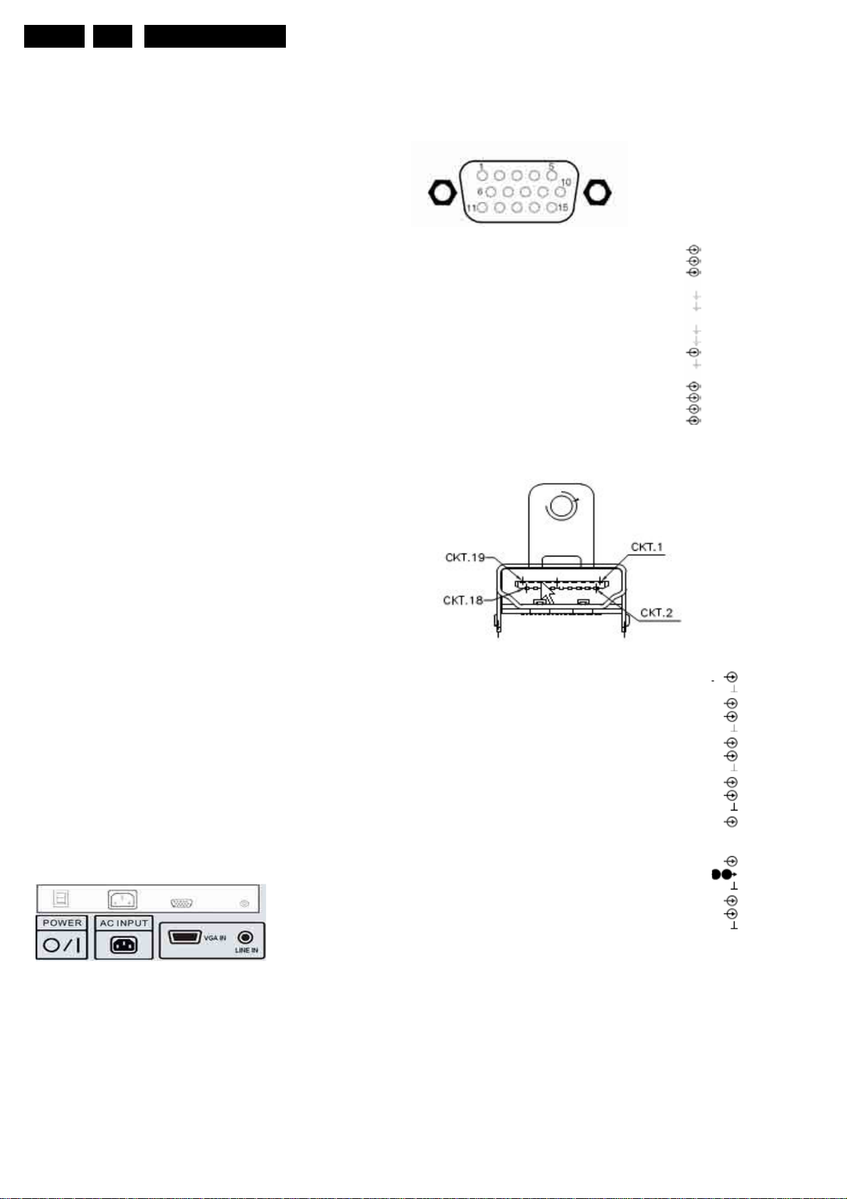
EN 1
1.1.3
1. Technical Specifications,Connections, and Chassi s Ove rv ie w
MQC3.0A LA
1. Technical Specifications, Connections, and Chassis Overview
Index of this chapter:
VGA:Video 2fh RGB In
1.1 Technical Specifications
1.2 Connections
1.3 Chassis Overview
Note: Figures below can deviate slightly from the actual
situation, due to the different set executions.
1.1 Technical Specifications
1.1.1 Vision
Display type
Screen size
Resolution
Contrast ratio
Light output (cd/m2)
Response time (ms)
Viewing angle
color systems
Video playback
Supported
:
: 32
:
inputs
:
:
:NTSC
:
:
:
:
LCD ( A UO )
inches (813.3 mm) diagonal
1366x768
1000:1
500 Cd/m²
12ms
88° (L) / 88° (R), 88° (U) / 88° (D) TV
NTSC, PAL, SECAM
480i
: 576i
: 480p
:576p
: 1080i
720p
:
Figure 1-2 VGAConnector
1 - Video Red 0.7 VPP / 75 ohm
2 - Video Green
3 - Video Blue 0.7 VPP / 75 ohm
4 – n.c
5 –Ground
6 -Ground Red Gnd
7 -Ground
Green
8 -Ground Blue Gnd
9 - +5V_DC +5VDC
10 -Gnd Sync Gnd
11 - n.c.
12 - DDC_SDA DDC data
13 - H-sync
14 - V-sync
15 - DDC_SCL DDC clock
HDMI Digital Video-In
Gnd
0 - 5V
0 - 5V
0.7 VPP / 75 ohm
Gnd
1.1.2 Sound
Sound systems
Internal speaker
volume adjustable
Miscellaneous
Power supply:
-AC Power voltage (VAC) : 90-264V
-AC Power frequency (Hz)
Ambient conditions:
-Temperature range
- Maximum humidity
Power consumption
- Normal operation
- Stand-by: < 2W
Dimensions(WxHxDcm)
Weight (kg)
:
:
:
: 235W
1.2 Connections
1.2.1 Rear I/O Connections
MTS (NTSC), FM-FM
: 10 W x 2 stereo,
0~35ĘC
10%~90%
: 47~63Hz
:17*29*3
:25.5kg
1-D2+
2
- Shield
3 - D24 - D1+
5 - Shield Gnd
6 - D17 - D0+
8 - Shield Gnd
9 - D010 - CLK+
11 - Shield Gnd
12 - CLK- Data channel
13 - n.c
14
15
6 - DDC_SDA
1
17 - Ground
18 - +5V
19 - HPD
20 - Ground
Gnd
Data channel
Data channel
Data channel
Data channel
Data channel
Data channel
-
n.c
- DDC_SCL
Gnd
Hot Plug D
Gnd
Data channel
DDC cloc
DDC data
k
etect
Figure 1-1 back
EN
Audio-In
Gn Stereo R/L Channels 500mVrms/22K ohm

A
A
A
A
d
1.2.2 Right I/O Connections
Technical Specifications, Con ne ction s,and Chassis Overview
EN2
1.
MQC3.0A LA
erial-In
-F-type 75ohm
V1-S1/AV2-S2: S-Video 1Fh Y/C-In
1-Ground Y Gnd
2-Ground C Gnd
3-Video Y 1Vpp/75 ohm
4-Video C 0.3Vpp/75 ohm
V1/AV2 Video In, Audio In
1-Audio R 0.5 Vrms/10Kohm
2-Gnd CVBS Gnd
3-Video CVBS 1Vpp/75 ohm
4-Audio L 0.5 Vrms/10Kohm
YPBPR1/YPBPR2
Wh….-Audio L 0.5 Vrms/10Kohm
Rd….-Audio R 0.5 Vrms/1 0 Ko hm
BuVideo Pb 0.7 Vpp/75 ohm
RdVideo Pr 0.7 Vpp/75 ohm
GnVideo Y 1Vpp/75 ohm
1.3 Chassis overview
udio Out
Level: 500 mVrms
Type: Stereo R/L Channels
Impedance: Low Impedance
Interface: RCA Jack, R: Red color, L: White color
Power board
Powerkey board
Main Board
AD6 CPU Board
Translation Board
Button boar

EN 3
y
r
A
A
A
A
2. Safet
MQC3.0A LA
Instructi o n s,Warnings, and Notes
2. Safety Instructions, Warnings, and Notes
2.1 Safety Instructions
Safety regulations require that during a repair:
•
Connect the set to the AC Power via an
isolation transformer (> 800 VA).
•
Replace safety components, indicated by the symbol ,
only by components identical to the original ones. Any
other component substitution (other than original type)
may increase risk of fire or
Safety regulations require that after a repair, the set must
be returned in its original condition. Pay in particula
attention to the following points:
•
Route the wire trees correctly and fix them with
the mounted cable clamps.
•
Check the insulation of the AC Power lead for
external damage.
•
Check the strain relief of the AC Power cord for
proper function.
•
Check the electrical DC resistance between the AC
Power plug and the secondary side (only for sets
have a AC Power isolated power supply):
1. Unplug the AC Power cord and connect a wire
between the two
2. Set the AC Power switch to the "on" position (keep the
AC Power cord unplugged!).
3. Measure the resistance value between the pins of the
AC Power plug and the metal shielding of the tuner or
the aerial connection on the set. The reading should
be between 4.5 Mohm and 12 Mohm.
4. Switch "off" the set, and remove the wire between the
two pins of the AC Power plug.
•
Check the cabinet for defects, to avoid touching of
any inner parts by the customer.
pins of the AC Power plug.
electrical shock hazard.
which
2.2 Warnings
• All ICs and many other semiconductors are susceptible to
electrostatic discharges (ESD ). Careless handling
during repair can reduce life drastically. Make sure
during repair,
as the mass of the set by a
Keep components and
Available ESD protection equipment:
– Complete kit ESD3 (small tablemat, wristband,
connection box,
4822
310 10671.
– Wristband tester 4822 344 13999.
•
Be careful during measurements in the high
voltage section.
•
Never replace modules or other components while the
unit is switched "on".
•
When you align the set, use plastic rather than metal
tools. This will prevent
of a circuit becoming unstable.
you are connected with the same potential
wristband with resistance.
tools also at this same potential.
extension cable and earth cable)
any short circuits and the danger
that,
2.3 Notes
2.3.1 General
• Measure the voltages and waveforms with regard to the
chassis (= tuner) ground
depending on the tested area of circuitry. The voltages and
waveforms
shown in the diagrams are indicative. Measure them in the
Service Default Mode (see chapter 5)
and stereo sound (L: 3 kHz, R: 1 kHz unless stated
otherwise) and
61.25 MHz for NTSC (channel 3).
(
), or hot ground (
with a color bar signal
picture carrier at 475.25 MHz for PAL, or
),
•
Where necessary, measure the waveforms and voltages
with
voltages in the power supply section both in normal
operation (
indicated by
• The semiconductors indicated in the circuit diagram and in the
parts lists, are interchangeable per position
semiconductors in the unit, irrespective of the type indication on
these semiconductors.
•
Manufactured under license from Dolby Laboratories.
“Dolby” and the “double-D symbol”, are trademarks of
Dolby Laboratories.
2.3.2 Schematic Not es
•
All resistor values are in ohms and the value multiplier is often
used to indicate the decimal point location (e.g. 2K2 indicates
2.2 Kohm).
•
Resistor values with no multiplier may be indicated with either
an "E"
•
All capacitor values are given in micro-farads (µ= x10-6),
nano-farads (n=
•
Capacitor values may also use the value multiplier as the
decimal point indication (e.g. 2p2 indicates 2.2 pF).
•
An "asterisk" (*) indicates component usage varies. Refer to
the diversity tables for the correct values.
•
The correct component values are listed in the Electrical
Replacement Parts List. Therefore, always check this list when
there is any doubt.
2.3.3 Rework on BGA (Ball Grid Array) ICs
General
lthough (LF)BGA assembly yields are very high, there may still be
a requirement for component rework. By
process of removing the component from the PWB and replacing it
with a new component. If an
solder balls of the component are deformed drastically so the
removed (LF)BGA has to be discarded.
Device Removal
s is the case with any component that, it is essential when
removing an (LF)BGA, the board,
surrounding components are not
(LF)BGA, the board must be uniformly heated to a temperature close
to the reflow soldering temperature. A uniform temperature reduces
the chance of warping the PWB.
To do this, we recommend that the board is heated until it is certain
that all the joints are molten. Then carefully
the board
profiles, see the IC data sheet.
rea Preparation
When the component has been removed, the vacant IC area
must be cleaned before replacing the (LF)BGA.
Removing an IC often leaves varying amounts of solder on the
mounting lands. This excessive
either a solder sucker or solder
removed
fter the board is properly cleaned and inspected, apply flux on
the solder lands and on the connection balls of the (LF)BGA.
Note: Do not apply solder paste, as this has shown to result in
problems during
(
) and without (
) and in stand-by ( ). These values are
means of the appropriate symbols.
or an "R" (e.g. 220E or 220R indicates 220 ohm).
with a vacuum nozzle. For the appropriate temperature
with a brush and cleaning agent.
re-soldering.
) aerial signal. Measure the
x10-9), or pico-farads (p= x10
(LF)BGA is removed from a PWB, the
tracks, solder lands, or
damaged. To remove an
solder can be removed with
wick. The remaining flux can be
with the
-12
).
rework, we mean the
pull the component off

Device Replacement
y
Y
p
The last step in the repair process is to solder the new
component on the board. Ideally, the (LF)BGA should be
aligned under a
possible, try to align the (LF)BGA
To reflow the solder, apply a temperature profile according to
the
IC data sheet. So as not to damage neighboring
components, it may be necessary
temperatures and times.
microscope or magnifying glass. If this is not
with any board markers.
to reduce some
More Information
For more information on how to handle BGA devices, visit this
URL:
www.atyourservice.ce.philips.com (needs subscription,
not available for all regions).
then go to “Workshop Information”. Here
Information on how
After login, select “Magazine”,
to deal with BGA-ICs.
you will find
2.3.4 Lead Free Solder
Philips CE is going to produce lead-free sets (PBF) from
1.1.2005 onwards.
Lead-free sets will be indicated by the PHILIPS-lead-free logo
on the Printed Wiring Boards (PWB):
Figure 2-1 Lead-fr ee logo
This sign normally has a diameter of 6 mm, but if there is less
space on a board also 3 mm is possible.
In case of doubt wether the board is lead-free or not (or with
mixed technologies),
• Always use the highest temperature to solder, when using
SAC305 (see also instructions below).
• De-solder thoroughly (clean solder joints to avoid mix of
two alloys).
Caution: For BGA-ICs, you must use the correct temperature
profile,which is coupled to the 12NC. For an overview of these
profiles, visit the website
You
will find this and more technical information within the
"Magazine", chapter "Workshop information".
For additional questions please contact your local repair-helpdesk.
you can use the following method:
http://www.atyourservice.ce.philips.com/
the workshop during a repair:
b
•
Use only lead-free soldering tin Philips SAC305 with order
code 0622 149 00106. If lead-free solder paste is required,
please contact the manufacturer of
equipment. In general, use of solder paste
workshops should be avoided because paste is not easy to
store and to handle.
•
Use only adequate solder tools applicable for
lead-free soldering tin. The solder tool must be able
– To reach at least a solder-tip temperature of 400°C.
– To stabilise the adjusted temperature at the solder-tip.
– To exchange solder-tips for different applications.
•
Adjust your solder tool so that a temperature around 360°C
-380°C is reached and stabilised
Heating time of the solder-joint should not exceed
Avoid temperatures above 400°C, otherwise
tips will rise drastically and flux-fluid will be destroyed. To
avoid wear-out
reduce heat.
•
Mix of lead-free soldering tin/parts with leaded soldering
tin/parts is possible but PHILIPS
avoid mixed regimes. If not to avoid, clean carefully the
solder-joint from
•
Use only original spare-parts listed in the
Service-Manuals. Not listed standard material
(commodities) has to be purchased at external companies.
Special information for lead-free BGA ICs: these ICs will
•
be delivered in so-called "dry-packaging" to protect the IC
against moisture. This packaging may only be opened
short before it is used (soldered). Otherwise the body of the
IC gets "wet" inside and during the heating time the
structure of the IC
)pressure inside the body. If the packaging was opened
before usage, the IC has to be heated up for some hours
(around 90°C) for drying (think of ESD-protection !).
Do not re-use BGAs at all!
•
For sets produced before 1.1.2005, containing leaded
soldering tin and components, all needed spare parts will
be available till the end of the
of such sets nothing changes.
of tips, switch “off” unused equipment or
old tin and re-solder with new tin.
will be destroyed due to high (steam-
2.3.5 Practical Service Precautions
•
It makes sense to avoid exposure to electrical shock.
While some sources are expected to have a possible
dangerous impact, others of quite
limited current and are sometimes held in less regard.
•
Always respect voltages
dangerous in themselves, they can cause unexpected
reactions - reactions that are best avoided. Before
into a powered TV set, it is best to test the high voltage
insulation. It is easy to do, and is a good service precaution.
MQC3.0A LA
Due to lead-free technology some rules
your soldering
within
at the solder joint.
recommends strongly to
service period. For the repair
high potential are of
. While some may not be
~ 4 sec.
wear-out of
reaching
EN4
3. Directions for Use
ou can download this information from the following websites:
htt
://www.philips.com/support
http://www.p4c.philips.com
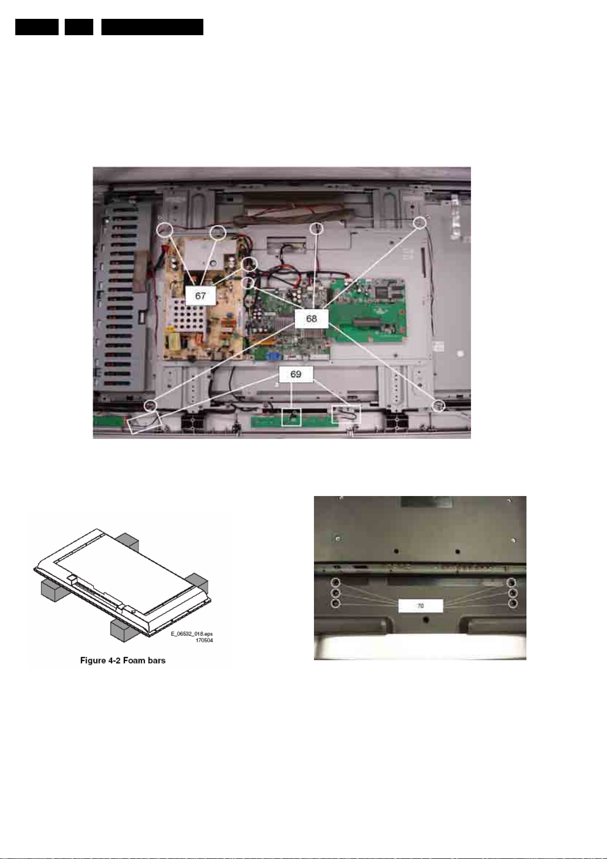
E EN5 4. MQC3.0A LA
m
Mechanical Instructions
4. Mechanical Instructions
Index of this chapter:
4.1 Cable Dressing
4.2 Service Positions
4.3 ASSY/PCBA Removal
4.1 Cable Dressing
4.2 Service Positions
4.2.1 Foa
The foam bars (order code 3122 785 90580 for two pieces) can
be used for all types and sizes of
face down on the (ESD protective) foam bars, a stable situation
is created to perform measurements and alignments.
By placing a mirror under the TV, you can monitor the screen.
Bars
Flat TVs. By laying the TV
4.2.2 Stands
Figure 4-3 Stands
The stands can be mounted with the back cover removed or still
left on. So, the stand can be used to store products or to do
measurements. It is also very suitable to perform duration tests
without taking much space, without having the risk of overheating
,or the risk of products falling. The stands can be mounted and
removed quick and easy
be tightened
figure above.
and loosened manually without the use of tools. See
with use of the delivered screws that can
Note: Only use the delivered screws to mount the monitor to
the stands

4.3 Assy/Panel removal
4.3.1 IO Box
Warning: Disconnect the AC Power cord before you open the
set.
1. Place the TV set upside down on a table top, using the foam
bars (see part "Foam Bars").
Caution: do not put pressure on the display, but let the monitor
lean on the speakers or the Front cover.
2. Remove M3*6(4 pieces) from IO Box and HDMI Box
4.3.2 R&L Speaker//Back cover
1. Remove T3*8 (8 pieces) screws from the R/L speaker
2. Remove all T4*12(12 pieces) screws from the Back cover.
3.Than, remove the M3.5*6(2 pieces) from the Back cover
4.Lift the back cover from the set. Make sure that wires and flat
foilsare not damaged during the back cover removal.
4.3.3 Wall mount
Mechanical Instructions
EN 6 4. MQC3.0A LA
4.3.4 Main Board
1. Disconnect all cable from Base unit
2. Remove the fixation screws
3. T a ke out M a in Board
4.3.5 IR Board
1. Remove the fixation screws
2. T a ke out M a in Board
4.3.6 Power Board
1. Remove the fixation screws
2. T a ke out M a in Board
4.3.7 Translation Board
1. Remove the fixation screws
2. T a ke out M a in Board
4.3.8 Power-Key Board
1. Remove the fixation screws
2. T a ke out M a in Board
4.3.9 Button Board
1. Remove the fixation screws
2. T a ke out M a in Board
1. Remove M3*4(14 pieces) screws from EMI shielding
2.
Remove Io Nut(2pieces) screw from
3. Lift the wall mount from chassis. Make sure wires are not
damaged during the back cover removal.
EMI shielding
4.3.11 LCD Panel
4.3.10 CPU Board
1. Remove the fixation screws
2. T a ke out M a in Board

m
bly
m
bly
m
bly
r
A
EN7 4. MQC3.0A LA
Instructions
Disasse
1. Place the TV set down on the foam bars. Place
the bars at the edges of the set, so they
support the front frame and not only the glass
plate!
2. Remove the inverter cable (1), Button cable (2), Power key cable (3)
from all
3. Remove the 4Pcs M4*12 screws ( 5) fr om
4. Remove the 8Pcs T4*6 scre ws (6) from panel BKT Lift the PCB tray
from the set.
during the PCB tray removal.
Asse
will
PCBA. Remove LVDS cable from LCD panel (4)
Make sure that wires and flat foils are not damaged
panel
Support BKT
T o re-assem b le the LCD panel, execute all
processes in reverse order.
Note:
.While re-assemble, make sure that all are placed
and
And connected in their original position. See figure
“Cable dressing”
.Pay special attention not to damage the EMC foams
at the SSB shielding. Check that EMC foams are put
4.3.12 HDMI Assy
Disasse
1. Remove the2 screws from HDMI box cover
4.3.13Tune
ssy
Disassembly
1. Remove the 3 screws from Tuner box cover
2. Remove the 3 screws form Tuner box
TOP
3. Removethe3 screws from shielding
2. Remove the 2 screws from
3. Remove the3 screws from shielding
4. Remove the3 screws from HDMI board
HDMI box TOP
3. Remove the 4 screws from Tuner board
 Loading...