

Page 1
Colour Television Chassis
19180_000_110818.eps19180_000_110818.eps
19180_000_110818.eps
110905
TPM6.1HE
LA
Contents Page
1. Revision List 2
2. Technical Specs, Diversity, and Connections 2
3. Precautions, Notes, and Abbreviation List 8
4. Mechanical Instructions 12
5. Service Modes, Error Codes, and Fault Finding 23
6. Alignments 32
7. Circuit Descriptions 34
8. IC Data Sheets 47
9. Block Diagrams
Wiring diagram PICO 22" 61
Wiring diagram PICO 26" 62
Wiring diagram Thriller HD 32" 63
Wiring diagram Thriller 42" 64
Block Diagram PICO 65
Block Diagram Thriller HD 66
Block Diagram Thriller 67
10. Circuit Diagrams and PWB Layouts Drawing PWB
A01 715G4635 PSU DLT, Pico 22"
A01 715G5148 PSU DLT, Pico 26" 71
A01 715G4973 PSU Thriller HD 32" 74
A01 715G4802 PSU Thriller 42" 77
B 715G4979 SSB Design Line Tilt, Pico 81
B 715G4722 SSB Berlinale 98
B 715G4609 SSB Thriller 116
J 715G3975 IR/LED board 134
J 715G4702 IR Thriller 136
11. Styling Sheets
PICO 22" 138
PICO 26" 139
Thriller HD 32" 140
Thriller 42" 141
68
69-70
72-73
75-76
79-80
96-97
114-115
132-133
135
137
©
Copyright 2012 Koninklijke Philips Electronics N.V.
All rights reserved. No part of this publication may be reproduced, stored in a
retrieval system or transmitted, in any form or by any means, electronic, mechanical,
photocopying, or otherwise without the prior permission of Philips.
Published by MB/ViW/SC 1262 BG TV Quality, the Netherlands Subject to modification EN 3122 785 19181
2012-Feb-17
Page 2
EN 2 TPM6.1HE LA1.
Revision List
1. Revision List
Manual xxxx xxx xxxx.0
• First release.
Manual xxxx xxx xxxx.1
• Chapter 2: Added the PSUs to table 2-1 Described Model
Numbers and Diversity.
• Chapter 4: Added section 4.6.1 Re-assembling PICO 26"
.
2. Technical Specs, Diversity, and Connections
Index of this chapter:
2.1 Technical Specifications
2.2 Directions for Use
2.3 Connections
2.4 Chassis Overview
2.1 Technical Specifications
For on-line product support please use the links in. Here is
product information available, as well as getting started, user
manuals, frequently asked questions and software & drivers.
Table 2-1 Described Model Numbers and Diversity
SSB 2 4 9 10 Schematics
CTN Styling
22PFL3233D/10 Pico
26PFL3233D/10 Pico
32PFL3233D/10 Thriller
42PFL3233D/10 Thriller
11.1
11.2
HD
11.3
11.4
Mechanics
715Gxxxx
Connection Overview
4979 2-34-1 4.3 4.3.7 9.1 10.1 10-5-1 10-5-2 10-5-3 10-5-4 10-5-5 10-5-6 10-5-7 10-5-8 10-5-9 10-5-10 10-5-11 10-5-12 10-5-13 10-5-14 10-5-15 - 10.8
4979 2-3 4-2 4.3 4.3.7 9.2 10.2 10-5-1 10-5-2 10-5-3 10-5-4 10-5-5 10-5-6 10-5-7 10-5-8 10-5-9 10-5-1010-5-11 10-5-12 10-5-13 10-5-14 10-5-15 - 10.8
4722 2-2 4-3 4.4 4.4.8 9.3 10.3 10-6-1 10-6-2 10-6-3 10-6-4 10-6-5 10-6-6 10-6-7 10-6-8 10-6-9 10-6-1010-6-11 10-6-12 10-6-13 10-6-14 10-6-15 10-6-16 10.9
4609 2-1 4-4 4.5 4.5.8 9.4 10.4 10-7-1 10-7-2 10-7-3 10-7-4 10-7-5 10-7-6 10-7-7 10-7-8 10-7-9 10-7-1010-7-11 10-7-12 10-7-13 10-7-14 10-7-15 10-7-16 10.9
Wire Dressing
PSU SSB IR
Wiring Diagram
Assembly Removal
LCD Removal
A01 (Adapter)
Notes:
• Figures can deviate due to the different set executions.
• Specifications are indicative (subject to change).
B01 (System Power 1)
B02 (System Power 2)
B03 (Peripheral)
B04 (Connector/USB)
B05 (Audio I/O)
B06 (Speaker)
B07 (Video I/O)
B08 (Scart)
B09 (VGA)
B10 (LVDS)
B11 (DRAM)
B12 (GPIO)
B13 (HDMI)
B14 (Demodulator)
B15 (Tuner)
B16 (T-con)
J (IR/LED)
Note: The given model numbers are subject to change.
2.2 Directions for Use
Directions for use can be downloaded from the following
websites:
http://www.philips.com/support
http://www.p4c.philips.com
2012-Feb-17
back to
div. table
Page 3
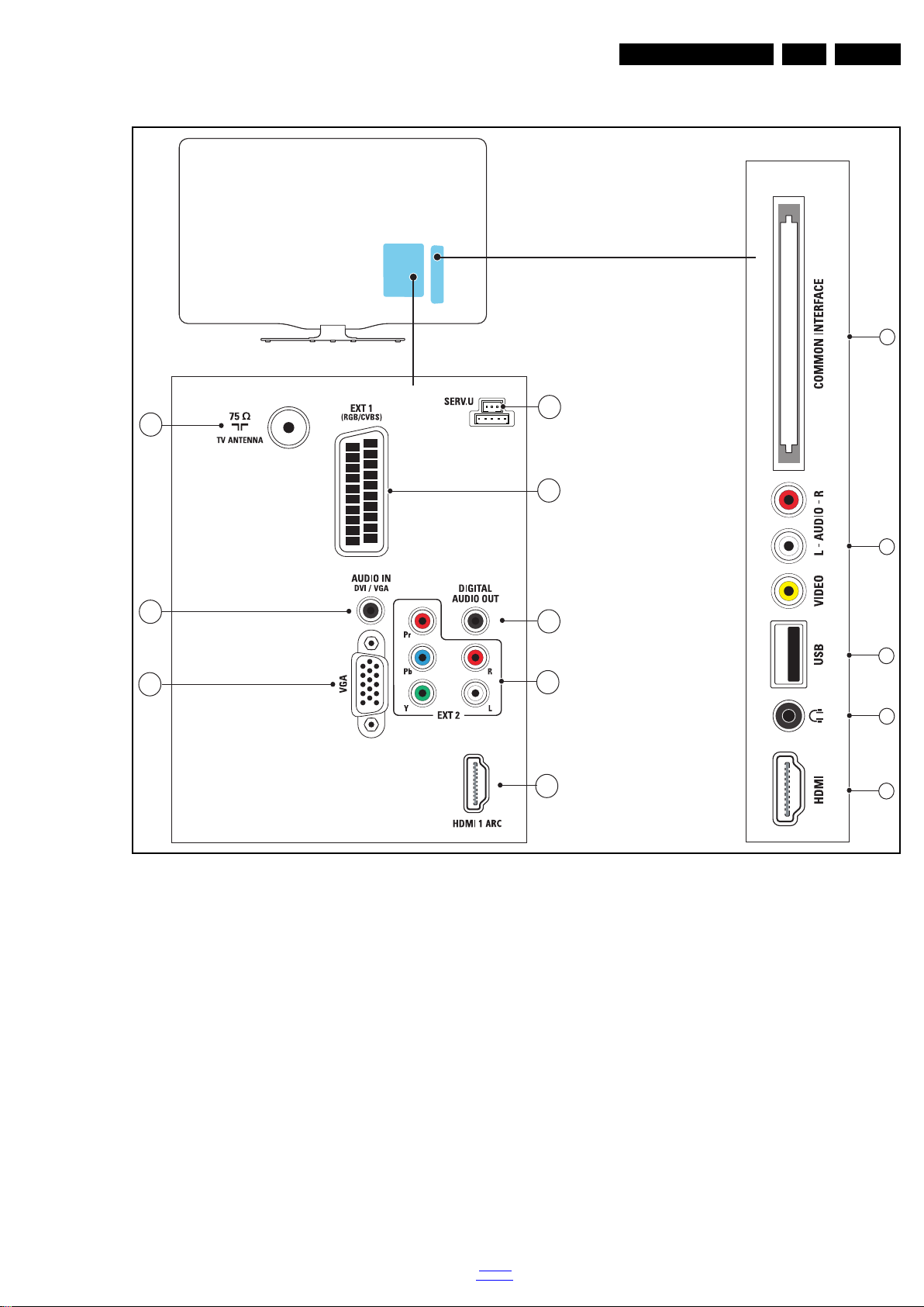
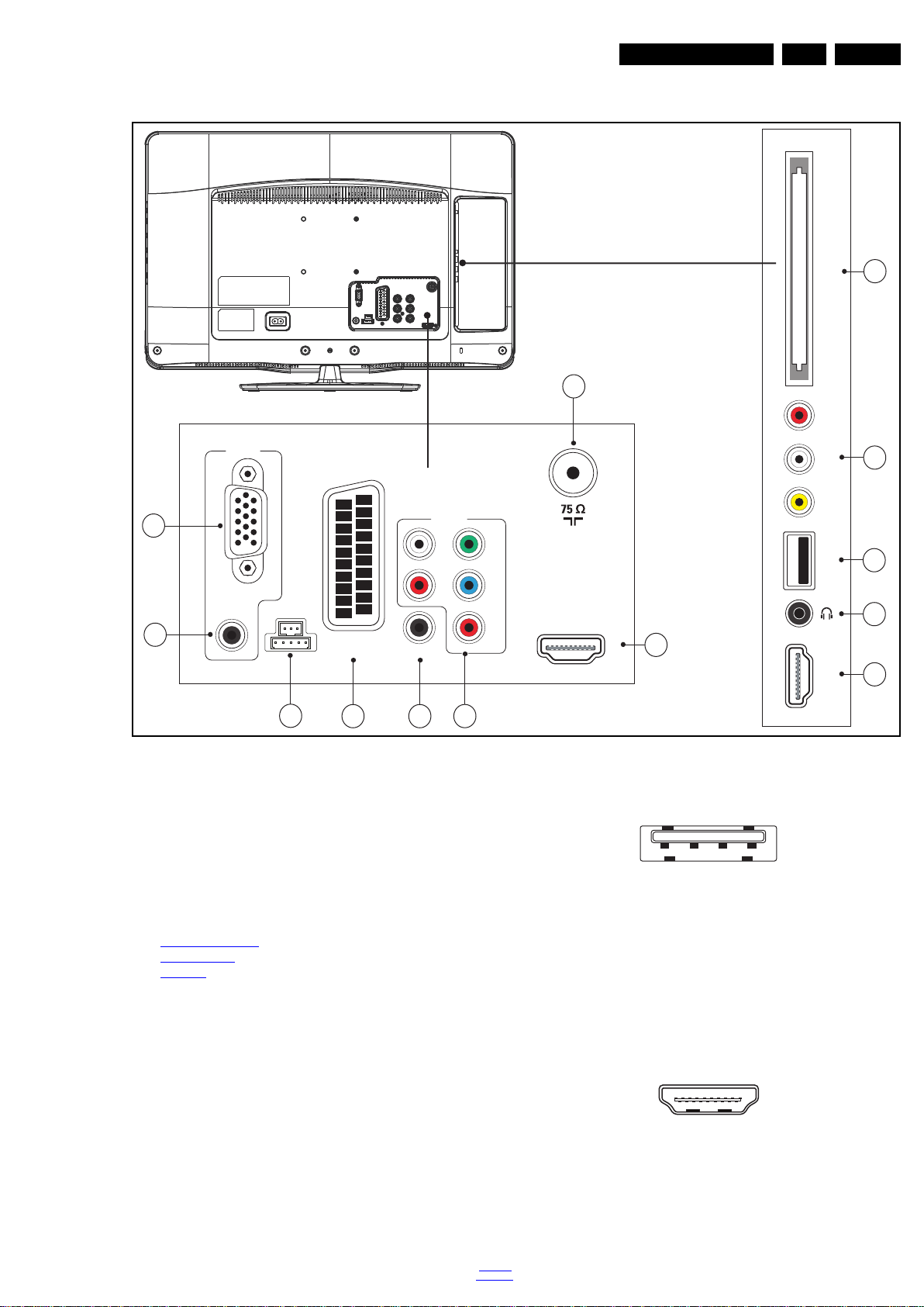
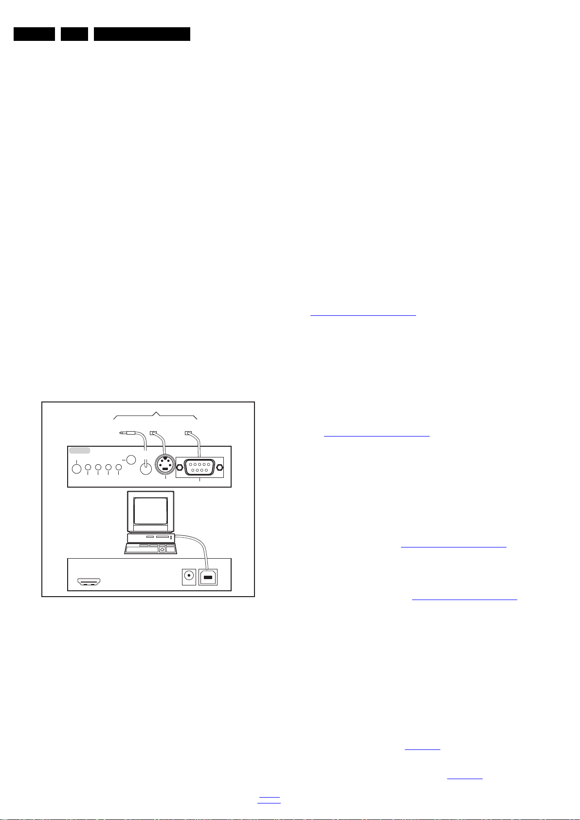
2.3 Connections
9
11
7
8
10
13
14
1
2
4
5
6
12
19080_001_110301.eps
110331
Technical Specs, Diversity, and Connections
EN 3TPM6.1HE LA 2.
Figure 2-1 Connection overview (Thriller styling)
back to
div. table
2012-Feb-17
Page 4
EN 4 TPM6.1HE LA2.
19082_002_110812.eps
110812
12
7
11109
13
8
1
3
4
5
6
Technical Specs, Diversity, and Connections
Figure 2-2 Connection overview (Thriller HD Styling)
2012-Feb-17
back to
div. table
Page 5
Technical Specs, Diversity, and Connections
AUDIO SERV.U
SPDIF
EXT 1
(RGB/CVBS)
HDMI 1
TV ANTENNA
EXT 2
Y L
Pb
Pr
R
VGA
PC IN
E C A F R E T N I N O M M O C O E D I V B S U I M D H O I D U A - L R -
19180_001_110818.eps
110905
12
1
2
8
4
5
6
10
13
6
14
11
15
1 2 3 4
10000_022_090121.eps
090121
10000_017_090121.eps
090428
19
1
18 2
EN 5TPM6.1HE LA 2.
2.3.1 Side Connections
Figure 2-3 Connection overview (PICO Styling)
Note: The following connector colour abbreviations are used
(according to DIN/IEC 757): Bk= Black, Bu= Blue, Gn= Green,
Gy= Grey, Rd= Red, Wh= White, Ye= Yellow.
1 - Common Interface
68p- See diagram
10-5-14 DVB T/C
Demodulator
MT5135. jk
2 - Cinch: Video CVBS - In, Audio - In
Ye -Video CVBS 1 V
Rd -Audio R 0.5 V
Wh -Audio L 0.5 V
3 - Service / UART
1 -Ground Gnd H
2 -UART_TX Transmit k
3 -UART_RX Receive j
/ 75 jq
PP
/ 10 k jq
RMS
/ 10 k jq
RMS
back to
div. table
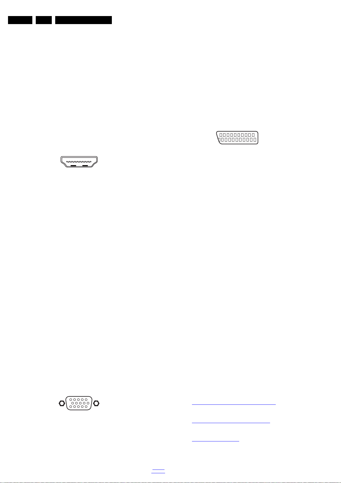
4 - USB2.0
Figure 2-4 USB (type A)
1-+5V k
2 -Data (-) jk
3 -Data (+) jk
4 -Ground Gnd H
5 - Head phone (Output)
Bk -Head phone 80 - 600 / 10 mW ot
6 - HDMI: Digital Video, Digital Audio - In
Figure 2-5 HDMI (type A) connector
1 -D2+ Data channel j
2 -Shield Gnd H
3 -D2- Data channel j
4 -D1+ Data channel j
2012-Feb-17
Page 6
EN 6 TPM6.1HE LA2.
10000_017_090121.eps
090428
19
1
18 2
1
6
10
11
5
15
10000_002_090121.eps
090127
Technical Specs, Diversity, and Connections
5-Shield Gnd H
6 -D1- Data channel j
7 -D0+ Data channel j
8-Shield Gnd H
9 -D0- Data channel j
10 - CLK+ Data channel j
11 - Shield Gnd H
12 - CLK- Data channel j
13 - Easylink/CEC Control channel jk
14 - n.c.
15 - DDC_SCL DDC clock j
16 - DDC_SDA DDC data jk
17 - Ground Gnd H
18 - +5V j
19 - HPD Hot Plug Detect j
20 - Ground Gnd H
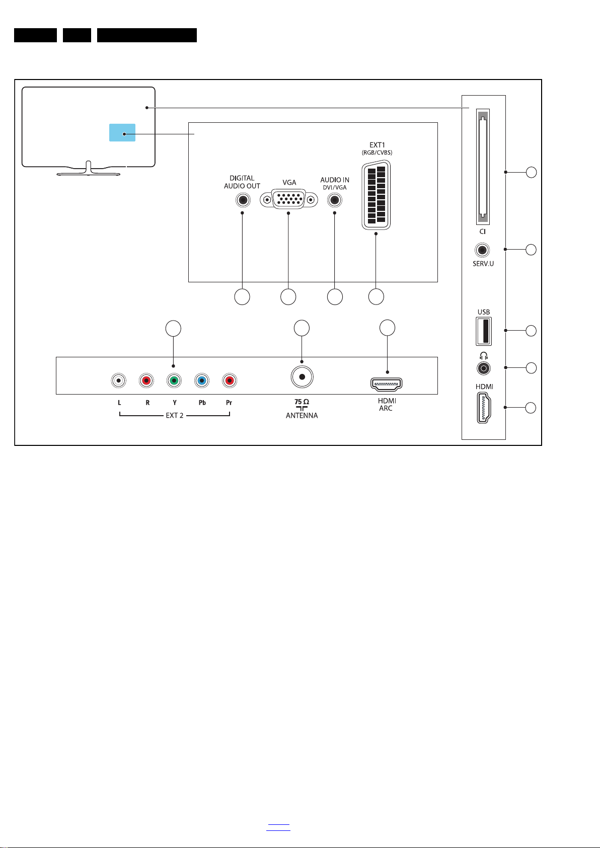
2.3.2 Rear Connections
7 - HDMI 1: Digital Video - In, Digital Audio with ARC - In/ Out
Figure 2-6 HDMI (type A) connector
1 -D2+ Data channel j
2-Shield Gnd H
3 -D2- Data channel j
4 -D1+ Data channel j
5-Shield Gnd H
6 -D1- Data channel j
7 -D0+ Data channel j
8-Shield Gnd H
9 -D0- Data channel j
10 - CLK+ Data channel j
11 - Shield Gnd H
12 - CLK- Data channel j
13 - Easylink/CEC Control channel jk
14 - ARC Audio Return Channel k
15 - DDC_SCL DDC clock j
16 - DDC_SDA DDC data jk
17 - Ground Gnd H
18 - +5V j
19 - HPD Hot Plug Detect j
20 - Ground Gnd H
5 -Ground Gnd H
6 -Ground Red Gnd H
7 -Ground Green Gnd H
8 -Ground Blue Gnd H
9-+5V
+5 V j
DC
10 - Ground Sync Gnd H
11 - Ground Red Gnd H
12 - DDC_SDA DDC data j
13 - H-sync 0 - 5 V j
14 - V-sync 0 - 5 V j
15 - DDC_SCL DDC clock j
11 - Audio - In: Left / Right, VGA
Gn - Audio L/R in 0.5 V
/ 10 k jq
RMS
12 - EXT1: Video RGB/YC - In, CVBS - In/Out, Audio - In/Out
20
21
10000_001_090121.eps
2
1
090121
Figure 2-8 SCART connector
1 -Audio R 0.5 V
2 -Audio R 0.5 V
3 -Audio L 0.5 V
/ 1 k k
RMS
/ 10 k j
RMS
/ 1 k k
RMS
4 -Ground Audio Gnd H
5 -Ground Blue Gnd H
6 -Audio L 0.5 V
7 -Video Blue/C-out 0.7 V
8 -Function Select 0 - 2 V: INT
/ 10 k j
RMS
/ 75 jk
PP
4.5 - 7 V: EXT 16:9
9.5 - 12 V: EXT 4:3 j
9 -Ground Green Gnd H
10 - n.c.
11 - Video Green 0.7 V
12 - n.c.
/ 75 j
PP
13 - Ground Red Gnd H
14 - Ground P50 Gnd H
15 - Video Red/C 0.7 V
16 - Status/FBL 0 - 0.4 V: INT
/ 75 j
PP
1 - 3 V: EXT / 75 j
17 - Ground Video Gnd H
18 - Ground FBL Gnd H
19 - Video CVBS 1 V
20 - Video CVBS/Y 1 V
21 - Shield Gnd H
/ 75 k
PP
/ 75 j
PP
8 - EXT2: Video YPbPr - In, Audio - In
Gn - Video - Y 1 V
Bu - Video - Pb 0.7 V
Rd -Video - Pr 0.7 V
Wh -Audio - L 0.5 V
Rd -Audio - R 0.5 V
9 - Cinch: Audio - Out
Rd -Audio R 0.5 V
Wh -Audio L 0.5 V
10 - PC IN:VGA
1 -Video Red 0.7 V
2 -Video Green 0.7 V
3 -Video Blue 0.7 V
4-n.c.
2012-Feb-17
/ 75 jq
PP
/ 75 jq
PP
/ 75 jq
PP
/ 10 k jq
RMS
/ 10 k jq
RMS
/ 10 k kq
RMS
/ 10 k kq
RMS
Figure 2-7 VGA connector
/ 75 j
PP
/ 75 j
PP
/ 75 j
PP
13 - TV ANTENNA - In
Signal input from an antenna, cable or satellite.
14 - Service / UART
1 -Ground Gnd H
2 -UART_TX Transmit k
3 -UART_RX Receive j
15 - Cinch: S/PDIF - Out
Bk -Coaxial 0.4 - 0.6V
2.3.3 Bottom Connections
7 - HDMI1: Digital Video, Digital Audio - In
See 6 - HDMI: Digital Video, Digital Audio - In
8 - EXT2: Video YPbPr - In, Audio - In
See 8 - EXT2: Video YPbPr - In, Audio - In
13 - TV ANTENNA - In
See 13 - TV ANTENNA - In
back to
div. table
/ 75 kq
PP
Page 7

Technical Specs, Diversity, and Connections
2.4 Chassis Overview
Refer to 9. Block Diagrams for PWB/CBA locations.
EN 7TPM6.1HE LA 2.
back to
div. table
2012-Feb-17
Page 8

EN 8 TPM6.1HE LA3.
Precautions, Notes, and Abbreviation List
3. Precautions, Notes, and Abbreviation List
Index of this chapter:
3.1 Safety Instructions
3.2 Warnings
3.3 Notes
3.4 Abbreviation List
3.1 Safety Instructions
Safety regulations require the following during a repair:
• Connect the set to the Mains/AC Power via an isolation
transformer (> 800 VA).
• Replace safety components, indicated by the symbol h,
only by components identical to the original ones. Any
other component substitution (other than original type) may
increase risk of fire or electrical shock hazard.
Safety regulations require that after a repair, the set must be
returned in its original condition. Pay in particular attention to
the following points:
• Route the wire trees correctly and fix them with the
mounted cable clamps.
• Check the insulation of the Mains/AC Power lead for
external damage.
• Check the strain relief of the Mains/AC Power cord for
proper function.
• Check the electrical DC resistance between the Mains/AC
Power plug and the secondary side (only for sets that have
a Mains/AC Power isolated power supply):
1. Unplug the Mains/AC Power cord and connect a wire
between the two pins of the Mains/AC Power plug.
2. Set the Mains/AC Power switch to the “on” position
(keep the Mains/AC Power cord unplugged!).
3. Measure the resistance value between the pins of the
Mains/AC Power plug and the metal shielding of the
tuner or the aerial connection on the set. The reading
should be between 4.5 M and 12 M.
4. Switch “off” the set, and remove the wire between the
two pins of the Mains/AC Power plug.
• Check the cabinet for defects, to prevent touching of any
inner parts by the customer.
3.2 Warnings
• All ICs and many other semiconductors are susceptible to
electrostatic discharges (ESD w). Careless handling
during repair can reduce life drastically. Make sure that,
during repair, you are connected with the same potential as
the mass of the set by a wristband with resistance. Keep
components and tools also at this same potential.
• Be careful during measurements in the high voltage
section.
• Never replace modules or other components while the unit
is switched “on”.
• When you align the set, use plastic rather than metal tools.
This will prevent any short circuits and the danger of a
circuit becoming unstable.
3.3 Notes
3.3.1 General
• Measure the voltages and waveforms with regard to the
chassis (= tuner) ground (H), or hot ground (I), depending
on the tested area of circuitry. The voltages and waveforms
shown in the diagrams are indicative. Measure them in the
Service Default Mode with a colour bar signal and stereo
sound (L: 3 kHz, R: 1 kHz unless stated otherwise) and
picture carrier at 475.25 MHz for PAL, or 61.25 MHz for
NTSC (channel 3).
• Where necessary, measure the waveforms and voltages
with (D) and without (E) aerial signal. Measure the
voltages in the power supply section both in normal
operation (G) and in stand-by (F). These values are
indicated by means of the appropriate symbols.
2012-Feb-17
3.3.2 Schematic Notes
• All resistor values are in ohms, and the value multiplier is
often used to indicate the decimal point location (e.g. 2K2
indicates 2.2 k).
• Resistor values with no multiplier may be indicated with
either an “E” or an “R” (e.g. 220E or 220R indicates 220 ).
• All capacitor values are given in micro-farads (10
nano-farads (n 10
• Capacitor values may also use the value multiplier as the
decimal point indication (e.g. 2p2 indicates 2.2 pF).
• An “asterisk” (*) indicates component usage varies. Refer
to the diversity tables for the correct values.
• The correct component values are listed on the Philips
Spare Parts Web Portal.
3.3.3 Spare Parts
For the latest spare part overview, consult your Philips Spare
Part web portal.
3.3.4 BGA (Ball Grid Array) ICs
Introduction
For more information on how to handle BGA devices, visit this
URL: http://www.atyourservice-magazine.com
“Magazine”, then go to “Repair downloads”. Here you will find
Information on how to deal with BGA-ICs.
BGA Temperature Profiles
For BGA-ICs, you must use the correct temperature-profile.
Where applicable and available, this profile is added to the IC
Data Sheet information section in this manual.
3.3.5 Lead-free Soldering
Due to lead-free technology some rules have to be respected
by the workshop during a repair:
• Use only lead-free soldering tin. If lead-free solder paste is
required, please contact the manufacturer of your soldering
equipment. In general, use of solder paste within
workshops should be avoided because paste is not easy to
store and to handle.
• Use only adequate solder tools applicable for lead-free
soldering tin. The solder tool must be able:
– To reach a solder-tip temperature of at least 400°C.
– To stabilize the adjusted temperature at the solder-tip.
– To exchange solder-tips for different applications.
• Adjust your solder tool so that a temperature of around
360°C - 380°C is reached and stabilized at the solder joint.
Heating time of the solder-joint should not exceed ~ 4 sec.
Avoid temperatures above 400°C, otherwise wear-out of
tips will increase drastically and flux-fluid will be destroyed.
To avoid wear-out of tips, switch “off” unused equipment or
reduce heat.
• Mix of lead-free soldering tin/parts with leaded soldering
tin/parts is possible but PHILIPS recommends strongly to
avoid mixed regimes. If this cannot be avoided, carefully
clear the solder-joint from old tin and re-solder with new tin.
3.3.6 Alternative BOM identification
It should be noted that on the European Service website,
“Alternative BOM” is referred to as “Design variant”.
The third digit in the serial number (example:
AG2B0335000001) indicates the number of the alternative
B.O.M. (Bill Of Materials) that has been used for producing the
specific TV set. In general, it is possible that the same TV
model on the market is produced with e.g. two different types
of displays, coming from two different suppliers. This will then
back to
div. table
-9
), or pico-farads (p 10
. Select
-12
-6
),
).
Page 9

Precautions, Notes, and Abbreviation List
10000_053_110228.eps
110228
EN 9TPM6.1HE LA 3.
result in sets which have the same CTN (Commercial Type
Number; e.g. 28PW9515/12) but which have a different B.O.M.
number.
By looking at the third digit of the serial number, one can
identify which B.O.M. is used for the TV set he is working with.
If the third digit of the serial number contains the number “1”
(example: AG1B033500001), then the TV set has been
manufactured according to B.O.M. number 1. If the third digit is
a “2” (example: AG2B0335000001), then the set has been
produced according to B.O.M. no. 2. This is important for
ordering the correct spare parts!
For the third digit, the numbers 1...9 and the characters A...Z
can be used, so in total: 9 plus 26= 35 different B.O.M.s can be
indicated by the third digit of the serial number.
Identification: The bottom line of a type plate gives a 14-digit
serial number. Digits 1 and 2 refer to the production centre (e.g.
SN is Lysomice, RJ is Kobierzyce), digit 3 refers to the B.O.M.
code, digit 4 refers to the Service version change code, digits 5
and 6 refer to the production year, and digits 7 and 8 refer to
production week (in example below it is 2010 week 10 / 2010
week 17). The 6 last digits contain the serial number.
Figure 3-1 Serial number (example)
3.3.7 Board Level Repair (BLR) or Component Level Repair (CLR)
If a board is defective, consult your repair procedure to decide
if the board has to be exchanged or if it should be repaired on
component level.
If your repair procedure says the board should be exchanged
completely, do not solder on the defective board. Otherwise, it
cannot be returned to the O.E.M. supplier for back charging!
3.3.8 Practical Service Precautions
• It makes sense to avoid exposure to electrical shock.
While some sources are expected to have a possible
dangerous impact, others of quite high potential are of
limited current and are sometimes held in less regard.
• Always respect voltages. While some may not be
dangerous in themselves, they can cause unexpected
reactions that are best avoided. Before reaching into a
powered TV set, it is best to test the high voltage insulation.
It is easy to do, and is a good service precaution.
3.4 Abbreviation List
0/6/12 SCART switch control signal on A/V
board. 0 = loop through (AUX to TV),
6 = play 16 : 9 format, 12 = play 4 : 3
format
AARA Automatic Aspect Ratio Adaptation:
algorithm that adapts aspect ratio to
remove horizontal black bars; keeps
the original aspect ratio
ACI Automatic Channel Installation:
algorithm that installs TV channels
directly from a cable network by
means of a predefined TXT page
ADC Analogue to Digital Converter
AFC Automatic Frequency Control: control
signal used to tune to the correct
frequency
AGC Automatic Gain Control: algorithm that
controls the video input of the feature
box
AM Amplitude Modulation
AP Asia Pacific
AR Aspect Ratio: 4 by 3 or 16 by 9
ASF Auto Screen Fit: algorithm that adapts
aspect ratio to remove horizontal black
bars without discarding video
information
ATSC Advanced Television Systems
Committee, the digital TV standard in
the USA
ATV See Auto TV
Auto TV A hardware and software control
system that measures picture content,
and adapts image parameters in a
dynamic way
AV External Audio Video
AVC Audio Video Controller
AVIP Audio Video Input Processor
B/G Monochrome TV system. Sound
carrier distance is 5.5 MHz
BDS Business Display Solutions (iTV)
BLR Board-Level Repair
BTSC Broadcast Television Standard
Committee. Multiplex FM stereo sound
system, originating from the USA and
used e.g. in LATAM and AP-NTSC
countries
B-TXT Blue TeleteXT
C Centre channel (audio)
CEC Consumer Electronics Control bus:
remote control bus on HDMI
connections
CL Constant Level: audio output to
connect with an external amplifier
CLR Component Level Repair
ComPair Computer aided rePair
CP Connected Planet / Copy Protection
CSM Customer Service Mode
CTI Color Transient Improvement:
manipulates steepness of chroma
transients
CVBS Composite Video Blanking and
Synchronization
DAC Digital to Analogue Converter
DBE Dynamic Bass Enhancement: extra
low frequency amplification
DCM Data Communication Module. Also
referred to as System Card or
Smartcard (for iTV).
DDC See “E-DDC”
D/K Monochrome TV system. Sound
carrier distance is 6.5 MHz
DFI Dynamic Frame Insertion
DFU Directions For Use: owner's ma nual
DMR Digital Media Reader: card reader
DMSD Digital Multi Standard Decoding
DNM Digital Natural Motion
back to
div. table
2012-Feb-17
Page 10

EN 10 TPM6.1HE LA3.
Precautions, Notes, and Abbreviation List
DNR Digital Noise Reduction: noise
reduction feature of the set
DRAM Dynamic RAM
DRM Digital Rights Management
DSP Digital Signal Processing
DST Dealer Service Tool: special remote
control designed for service
technicians
DTCP Digital Transmission Content
Protection; A protocol for protecting
digital audio/video content that is
traversing a high speed serial bus,
such as IEEE-1394
DVB-C Digital Video Broadcast - Cable
DVB-T Digital Video Broadcast - Terrestrial
DVD Digital Versatile Disc
DVI(-d) Digital Visual Interface (d= digital only)
E-DDC Enhanced Display Data Channel
(VESA standard for communication
channel and display). Using E-DDC,
the video source can read the EDID
information form the display.
EDID Extended Display Identification Data
(VESA standard)
EEPROM Electrically Erasable and
Programmable Read Only Memory
EMI Electro Magnetic Interference
EPG Electronic Program Guide
EPLD Erasable Programmable Logic Device
EU Europe
EXT EXTernal (source), entering the set by
SCART or by cinches (jacks)
FDS Full Dual Screen (same as FDW)
FDW Full Dual Window (same as FDS)
FLASH FLASH memory
FM Field Memory or Frequency
Modulation
FPGA Field-Programmable Gate Array
FTV Flat TeleVision
Gb/s Giga bits per second
G-TXT Green TeleteXT
H H_sync to the module
HD High Definition
HDD Hard Disk Drive
HDCP High-bandwidth Digital Content
Protection: A “key” encoded into the
HDMI/DVI signal that prevents video
data piracy. If a source is HDCP coded
and connected via HDMI/DVI without
the proper HDCP decoding, the
picture is put into a “snow vision” mode
or changed to a low resolution. For
normal content distribution the source
and the display device must be
enabled for HDCP “software key”
decoding.
HDMI High Definition Multimedia Interface
HP HeadPhone
I Monochrome TV system. Sound
2
C Inter IC bus
I
2
I
D Inter IC Data bus
2
S Inter IC Sound bus
I
carrier distance is 6.0 MHz
IF Intermediate Frequency
IR Infra Red
IRQ Interrupt Request
ITU-656 The ITU Radio communication Sector
(ITU-R) is a standards body
subcommittee of the International
Telecommunication Union relating to
radio communication. ITU-656 (a.k.a.
SDI), is a digitized video format used
for broadcast grade video.
Uncompressed digital component or
digital composite signals can be used.
2012-Feb-17
back to
div. table
The SDI signal is self-synchronizing,
uses 8 bit or 10 bit data words, and has
a maximum data rate of 270 Mbit/s,
with a minimum bandwidth of 135
MHz.
iTV Institutional TeleVision; TV sets for
hotels, hospitals etc.
LS Last Status; The settings last chosen
by the customer and read and stored
in RAM or in the NVM. They are called
at start-up of the set to configure it
according to the customer's
preferences
LATAM Latin America
LCD Liquid Crystal Display
LED Light Emitting Diode
L/L' Monochrome TV system. Sound
carrier distance is 6.5 MHz. L' is Band
I, L is all bands except for Band I
LPL LG.Philips LCD (supplier)
LS Loudspeaker
LVDS Low Voltage Differential Signalling
Mbps Mega bits per second
M/N Monochrome TV system. Sound
carrier distance is 4.5 MHz
MHEG Part of a set of international standards
related to the presentation of
multimedia information, standardised
by the Multimedia and Hypermedia
Experts Group. It is commonly used as
a language to describe interactive
television services
MIPS Microprocessor without Interlocked
Pipeline-Stages; A RISC-based
microprocessor
MOP Matrix Output Processor
MOSFET Metal Oxide Silicon Field Effect
Transistor, switching device
MPEG Motion Pictures Experts Group
MPIF Multi Platform InterFace
MUTE MUTE Line
MTV Mainstream TV: TV-mode with
Consumer TV features enabled (iTV)
NC Not Connected
NICAM Near Instantaneous Compounded
Audio Multiplexing. This is a digital
sound system, mainly used in Europe.
NTC Negative Temperature Coefficient,
non-linear resistor
NTSC National Television Standard
Committee. Color system mainly used
in North America and Japan. Color
carrier NTSC M/N= 3.579545 MHz,
NTSC 4.43= 4.433619 MHz (this is a
VCR norm, it is not transmitted off-air)
NVM Non-Volatile Memory: IC containing
TV related data such as alignments
O/C Open Circuit
OSD On Screen Display
OAD Over the Air Download. Method of
software upgrade via RF transmission.
Upgrade software is broadcasted in
TS with TV channels.
OTC On screen display Teletext and
Control; also called Artistic (SAA5800)
P50 Project 50: communication protocol
between TV and peripherals
PAL Phase Alternating Line. Color system
mainly used in West Europe (colour
carrier = 4.433619 MHz) and South
America (colour carrier
PAL M = 3.575612 MHz and
PAL N = 3.582056 MHz)
PCB Printed Circuit Board (same as “PWB”)
PCM Pulse Code Modulation
Page 11

Precautions, Notes, and Abbreviation List
EN 11TPM6.1HE LA 3.
PDP Plasma Display Panel
PFC Power Factor Corrector (or Pre-
conditioner)
PIP Picture In Picture
PLL Phase Locked Loop. Used for e.g.
FST tuning systems. The customer
can give directly the desired frequency
POD Point Of Deployment: a remova ble
CAM module, implementing the CA
system for a host (e.g. a TV-set)
POR Power On Reset, signal to reset the uP
PSDL Power Supply for Direct view LED
backlight with 2D-dimming
PSL Power Supply with integrated LED
drivers
PSLS Power Supply with integrated LED
drivers with added Scanning
functionality
PTC Positive Temperature Coefficient,
non-linear resistor
PWB Printed Wiring Board (same as “PCB”)
PWM Pulse Width Modulation
QRC Quasi Resonant Converter
QTNR Quality Temporal Noise Reduction
QVCP Quality Video Composition Processor
RAM Random Access Memory
RGB Red, Green, and Blue. The primary
color signals for TV. By mixing levels
of R, G, and B, all colors (Y/C) are
reproduced.
RC Remote Control
RC5 / RC6 Signal protocol from the remote
control receiver
RESET RESET signal
ROM Read Only Memory
RSDS Reduced Swing Differential Signalling
data interface
R-TXT Red TeleteXT
SAM Service Alignment Mode
S/C Short Circuit
SCART Syndicat des Constructeurs
d'Appareils Radiorécepteurs et
SCL Serial Clock I
Téléviseurs
SCL-F CLock Signal on Fast I
SD Standard Definition
SDA Serial Data I
SDA-F DAta Signal on Fast I
2
C
2
C bus
2
C
2
C bus
SDI Serial Digital Interface, see “ITU-656”
SDRAM Synchronous DRAM
SECAM SEequence Couleur Avec Mémoire.
Colour system mainly used in France
and East Europe. Colour
carriers = 4.406250 MHz and
4.250000 MHz
SIF Sound Intermediate Frequency
SMPS Switched Mode Power Supply
SoC System on Chip
SOG Sync On Green
SOPS Self Oscillating Power Supply
SPI Serial Peripheral Interface bus; a 4-
wire synchronous serial data link
standard
S/PDIF Sony Philips Digital InterFace
SRAM Static RAM
SRP Service Reference Protocol
SSB Small Signal Board
SSC Spread Spectrum Clocking, used to
reduce the effects of EMI
STB Set Top Box
STBY STand-BY
SVGA 800 × 600 (4:3)
SVHS Super Video Home System
SW Software
SWAN Spatial temporal Weighted Averaging
Noise reduction
SXGA 1280 × 1024
TFT Thin Film Transistor
THD Total Harmonic Distortion
TMDS Transmission Minimized Differential
Signalling
TS Transport Stream
TXT TeleteXT
TXT-DW Dual Window with TeleteXT
UI User Interface
uP Microprocessor
UXGA 1600 × 1200 (4:3)
V V-sync to the module
VESA Video Electronics Standards
Association
VGA 640 × 480 (4:3)
VL Variable Level out: processed audio
output toward external amplifier
VSB Vestigial Side Band; modulation
method
WYSIWYR What You See Is What You Record:
record selection that follows main
picture and sound
WXGA 1280 × 768 (15:9)
XTAL Quartz crystal
XGA 1024 × 768 (4:3)
Y Luminance signal
Y/C Luminance (Y) and Chrominance (C)
signal
YPbPr Component video. Luminance and
scaled color difference signals (B-Y
and R-Y)
YUV Component video
back to
div. table
2012-Feb-17
Page 12
EN 12 TPM6.1HE LA4.
19180_100_110823.eps
110823
Mechanical Instructions
4. Mechanical Instructions
Index of this chapter:
4.1 Cable Dressing
4.2 Service Positions
4.3 Assembly/Panel Removal (PICO styling)
4.4 Assembly/Panel Removal (Thriller HD styling)
4.5 Assembly/Panel Removal (Thriller styling)
4.1 Cable Dressing
4.6 Set Re-assembly
Notes:
• Figures below can deviate slightly from the actual situation,
due to the different set executions.
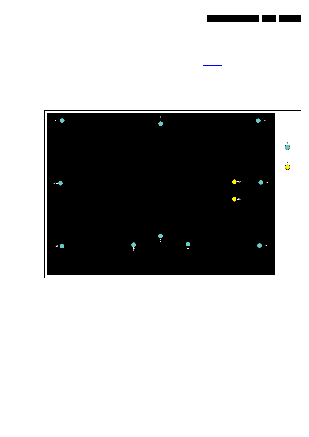
Figure 4-1 Cable dressing (22" PICO styling)
2012-Feb-17
back to
div. table
Page 13

Mechanical Instructions
19180_101_110823.eps
110823
19081_100_110609.eps
110803
EN 13TPM6.1HE LA 4.
Figure 4-2 Cable dressing (26" PICO styling)
Figure 4-3 Cable dressing (32" Thriller HD styling)
back to
div. table
2012-Feb-17
Page 14

EN 14 TPM6.1HE LA4.
19080_101_110302.eps
110302
Mechanical Instructions
Figure 4-4 Cable dressing (42" Thriller styling)
4.2 Se rvice Positions
For easy servicing of a TV set, the set should be put face down
on a soft flat surface, foam buffers or other specific workshop
tools. Ensure that a stable situation is created to perform
measurements and alignments. When using foam bars take
care that these always support the cabinet and never only the
display. Caution: Failure to follow these guidelines can
seriously damage the display!
Ensure that ESD safe measures are taken.
4.3 Assembly/Panel Removal (PICO styling)
Instructions below apply to the 22HFL3233D/10, but will be
similar for other models.
4.3.1 Rear Cover
Refer to Figure 4-5
Warning: Disconnect the mains power cord before removing
the rear cover.
1. Remove the fixation screw that secure the base.
2. Remove all plastite fixation screws [1] and metric fixation
screw [2] that secure the rear cover.
3. At the indicated areas [3] the cover is secured by clips. Be
very careful with releasing those.
4. Lift the rear cover from the TV. Make sure that wires and
flat foils are not damaged while lifting the rear cover from
the set.
for details.
2012-Feb-17
back to
div. table
Page 15

Mechanical Instructions
19180_104_110824.eps
110824
2
1
1
1
3
1
1
1
3
EN 15TPM6.1HE LA 4.
4.3.2 Small Signal Board (SSB)
Caution: it is mandatory to remount all different screws at their
original position during re-assembly. Failure to do so may result
in damaging the SSB.
1. Release the clips from both the LVDS Flat Foil connectors
that connect with the SSB.
Caution: be careful, as these are very fragile connectors!
Take the flat foils out of their connectors.
2. Unplug all other connectors.
3. Remove all fixation screws from the SSB.
4. Remove the screws between the side AV left and right
audio connectors.
5. Remove the SSB from the metal bracket.
4.3.3 Power Supply Unit (PSU)
Caution: it is mandatory to remount all different screws at their
original position during re-assembly. Failure to do so may result
in damaging the PSU.
1. Release the tape from the Power board cables.
2. Unplug power connectors from the SSB, as it is not unplugable at the PSU itself (soldered connector).
3. Unplug the other connectors from the PSU and the panel.
4. Remove all fixation screws from the PSU.
5. The PSU can be taken out of the set now.
When defective, replace the whole unit.
Figure 4-5 Rear cover removal
4.3.4 Speakers
1. Unplug the speaker connector from the SSB.
2. Release the cable from the clamp.
3. Take the left and right speakers out.
When defective, replace the both units.
4.3.5 IR/LED Board
1. Remove the screw.
2. Unplug the connectors from the IR/LED board and release
3. Take the IR/LED board out.
When defective, replace the whole unit.
4.3.6 Keyboard Control Panel
Refer to Figure 4-6
1. Unplug the connector [1] on the IR/LED board that leads to
2. Release the cable from its tape.
3. Put your thumbs against the front bezel while pulling the
When defective, replace the whole unit.
the clips that secure the IR/LED board.
.
the Local Control board, as it is not unplug-able at the Local
Control board itself (soldered connector).
Local Control board in the direction of the arrow.
back to
div. table
2012-Feb-17
Page 16

EN 16 TPM6.1HE LA4.
19180_105_110824.eps
110824
1
Mechanical Instructions
Figure 4-6 Keyboard Control Panel
2012-Feb-17
back to
div. table
Page 17
Mechanical Instructions
19081_101_110609.eps
110609
1
3 × 14
2 × 7
2
1
1
1
1
1
1
1
1
1
1
2
2
EN 17TPM6.1HE LA 4.
4.3.7 LCD Panel
1. Release the clamps from the IR/LED board cable.
2. Unplug the connector from the IR/LED board.
3. Release the clips from both the LVDS Flat Foil connectors.
Caution: be careful, as these are very fragile cables and
connectors! Take the flat foils out of their connectors.
4. Remove all fixation screws from the bezel.
5. Lift the LCD Panel with the metal frame from the bezel.
6. Remove all fixation screws from the metal frame.
7. Lift the metal frame from the LCD Panel.
When defective, replace the whole unit.
4.4 Assembly/Panel Removal (Thriller HD styling)
Instructions below apply to the 32HFL3233D/10, but will be
similar for other models.
4.4.1 Rear Cover
Refer to Figure 4-7
Warning: Disconnect the mains power cord before removing
the rear cover.
1. Remove all fixation screws [1] and [2] that secure the rear
cover.
2. Lift the rear cover from the TV. Make sure that wires are not
damaged while lifting the rear cover from the set.
for details.
4.4.2 Small Signal Board (SSB)
Caution: it is mandatory to remount all different screws at their
original position during re-assembly. Failure to do so may result
in damaging the SSB.
1. Release the clips from both the LVDS Flat Foil connectors
that connect with the SSB.
Caution: be careful, as these are very fragile connectors!
Take the flat foils out of their connectors.
2. Unplug all other connectors.
3. Remove all fixation screws from the SSB.
4. Take out the SSB together with bottom I/O bracket.
5. Remove the screws between the bottom Y-Pb and L-R
audio connectors.
6. Remove the bottom I/O bracket from the SSB.
4.4.3 Power Supply Unit (PSU)
Caution: it is mandatory to remount all different screws at their
original position during re-assembly. Failure to do so may result
in damaging the PSU.
Figure 4-7 Rear cover removal
1. Release the tape from the Power board cables.
2. Unplug power connectors from the PSU.
3. Unplug all other connectors from the PSU.
4. Remove all fixation screws from the PSU.
5. The PSU can be taken out of the set now.
When defective, replace the whole unit.
4.4.4 Stand removal
1. Remove the four fixation screws.
2. Take the stand out.
4.4.5 Speakers
1. Unplug the left and right speaker connectors from the SSB.
2. Remove the Stand as described earlier.
3. Release the cables from the clamp.
4. Release the tape from the cables.
5. Take the left and right speakers out.
When defective, replace the both units.
back to
div. table
2012-Feb-17
Page 18

EN 18 TPM6.1HE LA4.
4.4.6 IR/LED Board
1. Release the clips that secure the IR/LED board and take
the IR/LED board out.
2. Unplug both the connectors from the IR/LED board.
When defective, replace the whole unit.
4.4.7 Keyboard Control unit
1. Remove the speakers as described earlier.
2. Remove the stand as described earlier.
3. Remove the IR/LED board as described earlier.
4. Lift the LCD Panel from the bezel.
5. Gently release the clips that hold the board and take it out
from the bezel.
6. Unplug the connector from the keyboard control panel.
When defective, replace the whole unit.
Mechanical Instructions
2012-Feb-17
back to
div. table
Page 19
Mechanical Instructions
19180_102_110823.eps
110905
1
M4 × 9
3
3 × 11
2 × 12
2
1
1
1
1
2
2
2
2
3
2
2
2
2
2
2
2
2
EN 19TPM6.1HE LA 4.
4.4.8 LCD Panel
1. Remove the SSB as described earlier.
2. Remove the PSU as described earlier.
3. Remove the stand as described earlier.
4. Remove the speakers as described earlier.
5. Release the tapes from the cables of the IR/KEY board.
6. Release the clips from both the LVDS connectors.
Caution: be careful, as these are very fragile cables and
connectors! Take the flat foils out of their connectors.
7. Remove the screws at the bottom of the panel that secure
the panel with the bezel.
8. Lift the LCD Panel from the bezel.
When defective, replace the whole unit.
4.5 Assembly/Panel Removal (Thriller styling)
Instructions below apply to the 42HFL3233D/10, but will be
similar for other models.
4.5.1 Rear Cover
Refer to Figure 4-8
Warning: Disconnect the mains power cord before removing
the rear cover.
1. Remove fixation screws [1] that secure the base assembly,
pull out the base assembly from the set. Then remove the
fixation screws [2], [3] that secure the rear cover. Refer to
Figure 4-8
2. Lift the rear cover from the TV. Make sure that wires and
flat foils are not damaged while lifting the rear cover from
the set.
for details.
for details.
4.5.2 Small Signal Board (SSB)
Refer to Figure 4-9
Caution: it is mandatory to remount all different screws at their
original position during re-assembly. Failure to do so may result
in damaging the SSB.
1. Release the clips from both the LVDS Flat Foil connectors
that connect with the SSB [1].
Caution: be careful, as these are very fragile connectors!
Take the flat foils out of their connectors.
2. Release the clamps and unplug all other connectors [2].
3. Remove the fixation screw from the clamp near the bottom
of the SSB, and take the clamp out [3].
4. Release the tape near the bottom side of the set from the
LCD panel.
5. Remove all other fixation screws from the SSB [4].
6. Take out the SSB together with its shielding.
7. Remove the screw near the L/R audio connectors [5].
and Figure 4-10 for details.
Figure 4-8 Rear cover removal
8. The SSB can now be shifted from the side connector cover,
back to
div. table
then lifted and taken out of the shielding [6]. Refer to Figure
4-10 for details.
2012-Feb-17
Page 20
EN 20 TPM6.1HE LA4.
19080_103_110302.eps
110404
3
4
4
4
4
4
1
2
Mechanical Instructions
4.5.5 Speakers
1. Remove the SSB as described earlier.
2. Remove the stand as described earlier.
3. Release the tape from the cable.
4. Take the speakers out.
When defective, replace the both units.
Figure 4-9 SSB removal [1/2]
6
6
19080_104_110308.eps
Figure 4-10 SSB removal [2/2]
4.5.3 Power Supply Unit (PSU)
Caution: it is mandatory to remount all different screws at their
original position during re-assembly. Failure to do so may result
in damaging the PSU.
1. Release the Power board cables from their clamps.
2. Unplug power connectors from the SSB, as it is not unplugable at the PSU itself (soldered connector).
3. Unplug all other connectors from the PSU.
4. Remove all fixation screws from the PSU.
5. The PSU can be taken out of the set now.
4.5.4 Stand removal
5
110404
Caution: it is mandatory to remount all different screws at their
original position during re-assembly. Be sure to put the set in
the Service Position.
1. Remove the fixation screws.
2. Take the stand out.
2012-Feb-17
back to
div. table
Page 21
4.5.6 IR/LED Board
19180_103_110823.eps
110905
1
2
2
2
2
1
2
2
2
2
2
2
1
1
2
2
Mechanical Instructions
EN 21TPM6.1HE LA 4.
Refer to Figure 4-11
1. Remove the stand as described earlier.
2. Remove the speakers as described earlier.
3. Release the clamps that hold the boards cable.
4. Remove the fixation screws [1], [2] that secure the LCD
panel with the bezel.
5. Lift the LCD Panel from the bezel.
6. Gently release the clips that hold the board and take it out
from the bezel.
7. Unplug both the connectors from the IR/LED board.
When defective, replace the whole unit.
for details.
Figure 4-11 IR/LED removal
4.5.7 Keyboard Control unit
1. Remove the speakers as described earlier.
2. Remove the stand as described earlier.
3. Release the clamps that hold board cable.
4. Remove the fixation screws [1], [2] that secure the LCD
panel with the bezel. Refer to Figure 4-11
5. Lift the LCD Panel from the bezel.
6. Gently release the clips that hold the board and take it out
from the bezel.
7. Unplug the connector from the keyboard control panel.
When defective, replace the whole unit.
for details.
back to
div. table
2012-Feb-17
Page 22
EN 22 TPM6.1HE LA4.
19181_100_120208.eps
120208
1
4.5.8 LCD Panel
1. Remove the SSB as described earlier.
2. Remove the PSU as described earlier.
3. Remove the speakers as described earlier.
4. Remove the stand as described earlier.
5. Release the IR/LED board cable from its clamps and
unplug the IR/LED board cable.
6. Remove the fixation screws [1], [2] that secure the LCD
panel with the bezel. Refer to Figure 4-11
7. Lift the LCD Panel from the bezel.
8. Remove the fixation screws that secure the panel with the
metal subframe.
9. Release the clips from both the LVDS Flat Foil connectors
that connect with the LCD panel.
Caution: be careful, as these are very fragile connectors!
Take the flat foils out of their connectors.
When defective, replace the whole unit.
4.6 Set Re-assembly
To re-assemble the whole set, execute all processes in reverse
order.
4.6.1 Re-assembling PICO 26"
Mechanical Instructions
for details.
Refer to Figure 4-12
for details.
1. In case the LCD panel has been replaced take special care
of the cable dressing around the panel’s LVDS connector
[1]. Be sure the LVDS cable is not clamped below the metal
rim. See also Figure 4-2
.
Figure 4-12 Re-assembling PICO 26"
Notes:
• While re-assembling, make sure that all cables are placed
and connected in their original position. See Figure 4-1
Figure 4-4
.
to
• Pay special attention not to damage the EMC foams on the
SSB shields. Ensure that EMC foams are mounted
correctly.
2012-Feb-17
back to
div. table
Page 23

Service Modes, Error Codes, and Fault Finding
10000_038_090121.eps
090819
PHILIPS
MODEL:
32PF9968/10
PROD.SERIAL NO:
AG 1A0620 000001
040
39mm
27mm
(CTN Sticker)
Display Option
Code
5. Service Modes, Error Codes, and Fault Finding
Index of this chapter:
5.1 Test Points
5.2 Service Modes
5.3 Stepwise Start-up
5.4 Service Tools
5.5 Software Upgrading
5.6 Error Codes
5.7 The Blinking LED Procedure
5.8 Fault Finding and Repair Tips
5.1 Test Points
As most signals are digital, it will be difficult to measure
waveforms with a standard oscilloscope. However, several key
ICs are capable of generating test patterns, which can be
controlled via ComPair. In this way it is possible to determine
which part is defective.
Perform measurements under the following conditions:
• Service Default Mode.
• Video: Colour bar signal.
• Audio: 3 kHz left, 1 kHz right.
5.2 Service Modes
The Service Mode feature is split into four parts:
• Service Default Mode (SDM).
• Service Alignment Mode (SAM).
• Customer Service Mode (CSM).
• Computer Aided Repair Mode (ComPair).
SDM and SAM offer features, which can be used by the Service
engineer to repair/align a TV set. Some features are:
• A pre-defined situation to ensure measurements can be
made under uniform conditions (SDM).
• Activates the blinking LED procedure for error identification
when no picture is available (SDM).
• Make alignments (e.g. White Tone), reset the error buffer
(SAM).
• Display information (“SDM” or “SAM” indication in upper
right corner of screen, error buffer, software version,
operating hours, options and option codes, sub menus).
The CSM is a Service Mode that can be enabled by the
consumer. The CSM displays diagnosis information, which the
customer can forward to the dealer or call centre. In CSM
mode, “CSM”, is displayed in the top right corner of the screen.
The information provided in CSM and the purpose of CSM is to:
• Increase the home repair hit rate.
• Decrease the number of nuisance calls.
• Solved customers’ problem without home visit.
Life Timer
During the life time cycle of the TV set, a timer is kept (called
“Op. Hour”). It counts the normal operation hours (not the
Stand-by hours). The actual value of the timer is displayed in
SDM and SAM in a decimal value. Every two soft-resets
increase the hour by + 1. Stand-by hours are not counted.
Software Identification, Version, and Cluster
The software ID, version, and cluster will be shown in the main
menu display of SDM, SAM, and CSM.
The screen will show: “AAAAAB-XX.YY”, where:
• AAAAA is the chassis name: TPM61HE x.yy (Thriller),
TPM62HE x.yy (Thriller HD) and TPM63HE x.yy (PICO).
• B is the region indication: E = Europe, A = AP/China, U =
NAFTA, L = LATAM.
• XX is the main version number: this is updated with a major
change of specification (incompatible with the previous
software version). Numbering will go from 01 - 99 and
AA - ZZ.
- If the main version number changes, the new version
number is written in the NVM.
- If the main version number changes, the default settings
are loaded.
• YY is the sub version number: this is updated with a minor
change (backwards compatible with the previous
versions). Numbering will go from 00 - 99.
- If the sub version number changes, the new version
number is written in the NVM.
- If the NVM is fresh, the software identification, version,
and cluster will be written to NVM.
Display Option Code Selection
When after an SSB or display exchange, the display option
code is not set properly, it will result in a TV with “no display”.
Therefore, it is required to set this display option code after
such a repair.
To do so, press the following key sequence on a standard RC
transmitter: “062598” directly followed by MENU and “xxx”,
where “xxx” is a 3 digit decimal value of the panel type: see
column “Display Code” in Table 6-2
bottom of the cabinet. When the value is accepted and stored
in NVM, the set will switch to Stand-by, to indicate that the
process has been completed.
EN 23TPM6.1HE LA 5.
, or see sticker on the side/
5.2.1 General
ComPair Mode is used for communication between a computer
and a TV on I
2
C /UART level and can be used by a Service
engineer to quickly diagnose the TV set by reading out error
codes, read and write in NVMs, communicate with ICs and the
micro processor (PWM, registers, etc.), and by making use of
a fault finding database. It will also be possible to up and
download the software of the TV set via I
2
C with help of
ComPair. To do this, ComPair has to be connected to the TV
set via the ComPair connector, which will be accessible
through the rear of the set (without removing the rear cover).
Note: For the new model range, a new remote control (RC) is
used with some renamed buttons. This has an impact on the
activation of the Service modes. For instance the old “MENU”
button is now called “HOME” (or is indicated by a “house” icon).
Next items are applicable to all Service Modes or are general.
back to
div. table
Figure 5-1 Location of Display Option Code sticker
During this algorithm, the NVM-content must be filtered,
because several items in the NVM are TV-related and not SSB
related (e.g. Model and Prod. S/N). Therefore, “Model”
and “Prod. S/N” data is changed into “See Type Plate”. In case
a call centre or consumer reads “See Type Plate” in CSM
mode, he needs to look to the side/bottom sticker to identify the
set, for further actions.
2012-Feb-17
Page 24

EN 24 TPM6.1HE LA5.
19180_200_110818.eps
110818
191
80_201_110818.eps
110818
Service Modes, Error Codes, and Fault Finding
5.2.2 Service Default Mode (SDM)
Purpose
Set the TV in SDM mode in order to be able to create a
predefined setting for measurements to be made. In this
platform, a simplified SDM is introduced (without protection
override and without tuning to a predefined frequency).
Specifications
• Set linear video and audio settings to 50%, but volume to
25%. Stored user settings are not affected.
• All service-unfriendly modes (if present) are disabled, since
they interfere with diagnosing/repairing a set. These
service unfriendly modes are:
– (Sleep) timer.
– Blue mute/Wall paper.
– Auto switch “off” (when there is no “ident” signal).
– Hotel or hospital mode.
– Child lock or parental lock (manual or via V-chip).
– Skipping, blanking of “Not favourite”, “Skipped” or
“Locked” presets/channels.
– Automatic storing of Personal Preset or Last Status
settings.
– Automatic user menu time-out (menu switches back/
OFF automatically.
– Auto Volume levelling (AVL).
How to Activate SDM
To activate SDM, use the following methods:
• Press the following key sequence on the RC transmitter:
“062596”, directly followed by the “MENU” button.
Note: It is possible that, together with the SDM, the main
menu will appear. To switch it “off”, push the “MENU”
button again.
After activating this mode, “SDM” will appear in the upper left
corner of the screen (when a picture is available).
On Screen Menu
After activating SDM, the following items are displayed, with
“SDM” in the upper right corner of the screen to indicate that the
television is in Service Default Mode. Menu items and
explanation:
• xxxxx Operating hours (in decimal).
• AAAAAB-XX.YY See paragraph Software Identification,
Version, and Cluster for the SW name definition.
• ERR Shows all errors detected since the last time the
buffer was erased in format <xxx> <xxx> <xxx> <xxx>
<xxx> (five errors possible).
• OP Used to read-out the option bytes. Ten
codes (in two rows) are possible.
• Command MENU from the user remote will enter the
normal user menu (brightness, contrast, colour, etc...) with
“SDM” OSD remaining, and pressing MENU key again will
return to the last status of SDM again.
• To prevent the OSD from interfering with measurements in
SDM, command “OSD” or “i+” (“STATUS” or “INFO” for
NAFTA and LATAM) from the user remote will toggle the
OSD “on/off” with “SDM” OSD remaining always “on”.
• Press the following key sequence on the remote control
transmitter: “062596” directly followed by the OK button to
switch to SAM (do not allow the display to time out between
entries while keying the sequence). Remarks: new RC will
not have I+ button, but function still remains.
How to Exit SDM
• Switch the set to “standby” by pressing the standby button
on the remote control transmitter or on the television set.
• Via a standard customer RC-transmitter: key
in “00”-sequence.
Note: If the TV is switched “off” by a power interrupt while
in SDM, the TV will show up in the last status of SDM menu
as soon as the power is supplied again. The error buffer will
not be cleared.
5.2.3 Service Alignment Mode (SAM)
Purpose
• To modify the NVM.
• To display/clear the error code buffer.
• To perform alignments.
Specifications
• Operation hours counter (maximum five digits displayed).
• Software version, error codes, and option settings display.
• Error buffer clearing.
• Option settings.
• Software alignments (White Tone).
• NVM Editor.
• Set screen mode to full screen (all content is visible).
How to Activate SAM
To activate SAM, use one of the following methods:
• Press the following key sequence on the remote control
transmitter: “062596”, directly followed by the “OK” button.
Do not allow the display to time out between entries while
keying the sequence.
• Or via ComPair.
ntering SAM, the follo
After e
wing items are displayed,
with “SAM” in the upper right corner of the screen to indicate
that the television is in Service Alignment Mode.
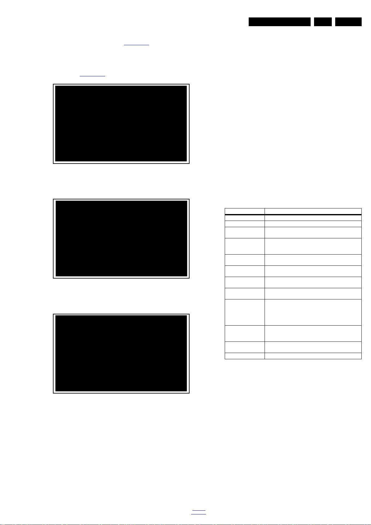
Figure 5-2 SDM menu
How to Navigate
As this mode is read only, there is not much to navigate. To
switch to other modes, use one of the following methods:
2012-Feb-17
back to
div. table
Figure 5-3 Example of SAM
Page 25
Service Modes, Error Codes, and Fault Finding
EN 25TPM6.1HE LA 5.
Table 5-1 SAM mode overview
Main Menu Sub-menu 1 S ub-menu 2 Description
System Information Op Hour This represents the life timer. The timer counts
Main SW ID e.g. “TPM62HE1.166B” See paragraph Software Identification, Version,
ERR e.g. “000 000 000 000 000” Shows all errors detected since the last time the
OP1 e.g. “012 004 192 002 184 032 007 030” Used to read-out the option bytes. See paragraph
OP2 e.g. “056 023 000 106 064 000 000 122”
Clear Press [OK] to clean the Error Codes immediately Erases the contents of the error buffer. Select this
RGB Align Warm R Gain To align the White Tone. See paragraph
G Gain
B Gain
Normal R Gain
G Gain
B Gain
Cool R Gain
G Gain
B Gain
Store Store the RGB value
NVM editor Address Select and fill the NVM address
Value Select and fill the NVM value
Store Store the value in the address
Upload to USB Copy Channel List to USB To upload several settings from the TV to an USB
Copy NVM to USB
Copy Readable Info to USB
Copy Edid to USB
Download from USB Copy Channel List from USB To download several settings from the USB stick to
Copy NVM from USB
Copy Readable Info from USB
Copy Edid from USB
Initialize NVM Press [OK] to Initialize NVM immediately To initialize a (corrupted) NVM. Be careful, this will
EDID Write Enable Press [OK] to enable EDID writable immediately Enable EDID writable
Service Data Type Number Press [OK] use key pad edit t ype number immediately Use Key pad to edit several ser vice data
Production Number Press [OK] use key pad edit production number immediately
12NC SSB Press [OK] use key pad edit SSB immediately
12NC PSU Press [OK] use key pad edit PSU immediately
12NC Display Press [OK] use key pad edit display immediately
Clear OAD Version Press [OK] to clean OAD Version immediately Clean OAD Version
normal operation hours, but does not count Standby hours.
and Cluster for the SW name definition.
buffer was erased. Five errors possible.
6.4 Option Settings
detailed description. Ten codes are possible.
menu item and press the MENU RIGHT key on the
remote control. The content of the error buffer is
cleared.
6.3 Software Alignments
for a detailed description
stick
the TV
erase all settings.
in the Alignments section for a
in chapter 6. Alignments
How to Navigate
• In the SAM menu, select menu items with the UP/DOWN
keys on the remote control transmitter. The selected item
will be indicated. When not all menu items fit on the screen,
use the UP/DOWN keys to display the next/previous menu
items.
• With the “LEFT/RIGHT” keys, it is possible to:
– (De) activate the selected menu item.
– (De) activate the selected sub menu.
– Change the value of the selected menu item.
• When you press the MENU button twice while in top level
SAM, the set will switch to the normal user menu (with the
SAM mode still active in the background). To return to the
SAM menu press the MENU button.
• The “INFO [i+]” key from the user remote will toggle the
OSD “on/off” with “SAM” OSD remaining always “on”.
• Press the following key sequence on the remote control
transmitter: ì062596î directly followed by the MENU button
to switch to SDM (do not allow the display to time out
between entries while keying the sequence). Remarks:
new RC will not have I+ button, but function still remain.
How to Store SAM Settings
To store the settings changed in SAM mode (except the
RGB ALIGN settings), leave the top level SAM menu by using
the POWER button on the remote control transmitter or the
television set. The mentioned exceptions must be stored
separately via the STORE button.
How to Exit SAM
Use one of the following methods:
• Switch the set to “standby” by pressing the mains button on
the remote control transmitter or the television set.
• Via a standard RC-transmitter, key in “00” sequence.
Note: When the TV is switched “off” by a power interrupt while
in SAM, the TV will show up in “normal operation mode” as
soon as the power is supplied again. The error buffer will not be
cleared.
5.2.4 Customer Service Mode (CSM)
Purpose
The Customer Service Mode shows error codes and
information on the TVs operation settings.The call centre can
instruct the customer (by telephone) to enter CSM in order to
identify the status of the set.This helps the call centre to
diagnose problems and failures in the TV set before making a
service call.
The CSM is a read-only mode; therefore, modifications are not
possible in this mode.
Specifications
• Ignore “Service unfriendly modes”.
• Line number for every
line (to make CSM language independent).
• Set the screen mode to full
screen (all contents on screen is visible).
back to
div. table
2012-Feb-17
Page 26

EN 26 TPM6.1HE LA5.
191
80_203_110818.eps
110818
191
80_204_110818.eps
110818
Service Modes, Error Codes, and Fault Finding
• After leaving the Customer Service Mode, the original
settings are restored.
• Possibility to use “CH+” or “CH-” for channel surfing, or
enter the specific channel number on the RC.
How to Activate CSM
To activate CSM, press the following key sequence on a
standard remote control transmitter: “123654”
(do not allow the display to time out between entries while
keying the sequence). After entering the Customer Service
Mode, the following items are displayed.
Note: Activation of the CSM is only possible if there is no (user)
menu on the screen!
19180_202_110818.eps
110818
Figure 5-4 CSM Menu [1/3]
replaced or is initialized after corruption, this production
code has to be re-written to NVM.
• 1.3 Installation date Indicates the date of the first
installation of the TV. This date is acquired via time
extraction.
• 1.4 Option Code 1 Gives the option codes of option group
1 as set in SAM.
• 1.5 Option Code 2 Gives the option codes of option group
2 as set in SAM.
• 1.6 SSB Gives an identification of the SSB as stored in
NVM. Note that if an NVM is replaced or is initialized after
corruption, this identification number has to be re-written to
NVM. This identification number is the 12NC number of the
SSB.
• 1.7 Display 12NC NVM read/write.
• 1.8 PSU 12NC NVM read/write.
• 2.1 Current Main SW Displays the built-in main software
version. In case of field problems related to software,
software can be upgraded. As this software is consumer
upgradeable, it will also be published on the Internet.
• 2.2 Standby SW Displays the built-in stand-by processor
software version. Upgrading this software will be possible
via USB.
• 2.3 Panel Code Displays the Display Code number.
• 2.4 NVM version Detects and displays NVM version.
• 2.5 Current CHTB Identifier Display current channel table
identifier.
• 2.6 Current SSB Identifier Display SSB identifier.
• 2.7 Room ID Display current Room ID.
• 3.1 Signal Quality/Present Analog/digital signal strength.
• 3.2 Child lock Not active / active. This is a combined item
for locks. If any lock (channel lock, parental lock) is active,
the item shall show “active”.
• 3.3 HDCP keys
are valid or no
Indicates if the HDMI keys (or HDCP keys)
t. In ca
se these keys are not valid and the
customer wants to make use of the HDMI functionality, the
SSB has to be replaced.
Figure 5-5 CSM Menu [2/3]
Figure 5-6 CSM Menu [3/3]
Contents of CSM
• 1.1 Set Type This information is very helpful for a
helpdesk/workshop as reference for further diagnosis. In
this way, it is not necessary for the customer to look at the
rear of the TV-set. Note that if an NVM is replaced or is
initialized after corruption, this set type has to be re-written
to NVM.
• 1.2 Production code Displays the production
code (the serial number) of the TV. Note that if an NVM is
How to Navigate
By means of the “CURSOR-DOWN/UP” knob (or the scroll
wheel) on the RC-transmitter, can be navigated through the
menus.
How to Exit CSM
To exit CSM, use one of the following methods.
• Press the MENU/HOME button on the remote control
transmitter.
• Press the POWER button on the remote control
transmitter.
• Press the POWER button on the television set.
2012-Feb-17
back to
div. table
Page 27

5.3 Stepwise Start-up
19080_206_110323.eps
110401
Power Off
Standby
Soft Mode
Power On
Semi-
Standby
Standby
Switch
Off(Mains
Power Plug)
Standby Soft Mode
Command Received,
previously in Standby
Soft Mode (Power tact
switch)
TV Wakeup
commands
Received
(TV Wakeup
keys)
Digital
background
tasks started
Digital
background
tasks completed
Swith On,
previously in
Standby/Semi-
Standby (Mains
Power Plug)
Standby
Soft Mode
Command
Received
(Power tact
switch)
Switch Off (Mains
Power Plug)
Switch Off
(Mains Power
Plug)
Swith On,
previously in
Standby Soft Mode
(Mains Power Plug)
Standby
commands
Received (RC
Standby key)
Standby Soft Mode
Command Received,
previously in Standby
Soft Mode (Power
tact switch)
TV Wakeup
commands
Received
(TV Wakeup
keys)
Switch On, previously
in Power On Mode
(Power tact switch)
Standby Soft Mode
Command Received,
(Power tact switch)
Switch Off (Mains
Power Plug)
Swith On,previously in
TV Operation Mode
(Mains Power Plug)
Service Modes, Error Codes, and Fault Finding
EN 27TPM6.1HE LA 5.
Figure 5-7 Stepwise Start-up
back to
div. table
2012-Feb-17
Page 28
EN 28 TPM6.1HE LA5.
Service Modes, Error Codes, and Fault Finding
5.4 Service Tools
5.4.1 ComPair
Introduction
ComPair (Computer Aided Repair) is a Service tool for Philips
Consumer Electronics products. and offers the following:
1. ComPair helps to quickly get an understanding on how to
repair the chassis in a short and effective way.
2. ComPair allows very detailed diagnostics and is therefore
capable of accurately indicating problem areas. No
knowledge on I
because ComPair takes care of this.
3. ComPair speeds up the repair time since it can
automatically communicate with the chassis (when the
microprocessor is working) and all repair information is
directly available.
4. ComPair features TV software up possibilities.
Specifications
ComPair consists of a Windows based fault finding program
and an interface box between PC and the (defective) product.
The ComPair II interface box is connected to the PC via an
USB cable. For the TV chassis, the ComPair interface box and
the TV communicate via a bi-directional cable via the service
connector(s).
The ComPair fault finding program is able to determine the
problem of the defective television, by a combination of
automatic diagnostics and an interactive question/answer
procedure.
How to Connect
This is described in the chassis fault finding database in
ComPair.
2
C or UART commands is necessary,
Note: When you encounter problems, contact your local
support desk.
Additional cables for VCOM Alignment
• ComPair/I2C interface cable: 3122 785 90004.
• ComPair/VGA adapter cable: 9965 100 09269.
Note: When you encounter problems, contact your local
support desk.
5.5 Software Upgrading
5.5.1 Description
It is possible for the user to upgrade the main software via the
USB port. This allows replacement of a software image in a
stand alone set. A description on how to upgrade the main
software can be found in the DFU or on the Philips website.
5.5.2 Introduction
Philips continuously tries to improve its products, and it’s
recommend that the TV software is updated when updates are
available. Software update files can be obtained from the
dealer or can be downloaded from the following websites:
http://www.philips.com/support
Preparing a portable memory for software upgrade
The following requirements have to be met:
1. A personal computer connected to the Internet.
2. An archive utility that supports the ZIP-format (e.g. WinZip
for Windows or Stufflt for Mac OS).
3. A USB flash drive (preferably empty).
TO TV
TO
TO
UART SERVICE
CONNECTOR
2
I
C
RS232 /UART
ComPair II Developed by Philips Brugge
Optional power
5V DC
10000_036_090121.eps
091118
ComPair II
RC in
Optional
Switch
Power ModeLink/
Activity
HDMI
2
I
C only
UART SERVICE
CONNECTOR
RC out
TO
I2C SERVICE
CONNECTOR
Multi
function
PC
Figure 5-8 ComPair II interface connection
Caution: It is compulsory to connect the TV to the PC as
shown in the picture above (with the ComPair interface in
between), as the ComPair interface acts as a level shifter. If
one connects the TV directly to the PC (via UART), ICs can be
blown!
Note:
1. Only FAT/DOS-formatted flash drives are supported.
2. Only use software update files that can be found on the
http://www.philips.com/support
web site.
5.5.3 Check the current TV software version
Before starting the software upgrade procedure, it is advised to
check that what the current TV software:
1. Press the “1 2 3 6 5 4” button on the remote control to enter
the CSM mode.
2. Use the up/down cursor keys to select “Current Main
Software”.
If the current software version of the TV is the same as the
latest update file found on http://www.philips.com/support
not necessary to update the TV software.
5.5.4 Download the latest software
1. Point the web browser to http://www.philips.com/support
2. Find information and software related to the TV.
3. Select the latest software update file and download it to the
PC.
4. Insert a USB flash drive into one of the USB ports of the
PC.
5. Decompress the downloaded ZIP file and copy the
“autorun.upg” to the root directory of the USB flash drive.
5.5.5 Update the TV software
, it is
.
How to Order
ComPair II order codes:
• ComPair II interface: 3122 785 91020.
• Software is available via the Philips Service web portal.
• ComPair UART interface cable for TPM6.1Hx xx.
(using DB9 to 2mm pitch JST connector): 3122 785 90630.
2012-Feb-17
back to
div. table
1. Insert mains power and wait for system to boot completely.
2. Insert the USB flash drive that contains the software
update files.
3. The TV will detect the USB flash drive automatically. Then
a window jumps out as Figure 5-9
.
Note: If the USB flash drive is not detected after power up,
disconnect it and re-insert it.
4. Select [Update] and press OK. See Figure 5-9
.
Page 29
Service Modes, Error Codes, and Fault Finding
19080_207_110324.eps
110324
19080_208_110324.eps
110324
19080_209_110324.eps
110324
EN 29TPM6.1HE LA 5.
5. To proceed, In next menu select [Start] and press OK to
start software updates. See Figure 5-10
.
6. Upgrading will now begins and the status of the updating
progress will be displayed.
7. When the TV software is updated. Remove your USB flash
drive, then select [Restart] and press OK to restart the
TV.See Figure 5-11
.
Figure 5-9 Update the TV software [1/3]
Figure 5-10 Update the TV software [2/3]
5.5.6 Content and Usage of the One-Zip Software File
Below you find a content explanation of the One-Zip file, and
instructions on how and when to use it. Only files that are
relevant for Service are mentioned here.
• EDID_clustername.zip: Contains the EDID content of the
different EDID NVMs. See ComPair for further instructions.
• FUS_clustername_version.zip: Contains the
“autorun.upg” which is needed to upgrade the TV main
software and the software download application.
• NVM_clustername_version.zip: Default NVM content.
Must be programmed via ComPair.
5.5.7 How to Copy NVM Data to/from USB
When copying data to and from a USB memory stick, the folder
“repair” is used. When inserting an empty USB memory stick,
and downloading data to the stick, the TV will create this folder.
When sending data from a USB memory stick to a TV, the
intended data must be available in the “repair” folder.
Note that when copying EDID data to the TV, all necessary
EDID files must be in this folder.
Service mode overview for your reference. Please adapt
accordingly:
Table 5-2 Service mode overview
Service Modes Description
SAM Service alignment mode
SDM Service defa ult Mode
CSM 3-page compact CSM pages. There will be CSM dump to
USB SW upgradeable SW-upgrading of flash m emories MTK-chips MT5366 can
NVM-Editor in SAM NVM-editor will function as in the past: Address and Value
Service Data New Service data in SAM for CTN, Prod. no., 12NC
USB copy/paste in
SAM
UART logging There will be printout available in UART. No specifications
Vcom flicker alignment “147852” + “OK” (for flickering adjustment).
Tcon NVM default &
Programmer default
loading
Blind SAM RC sequence “062598” + “Menu” +
Clear Buffer RC sequence “062599” + “OK” or via SAM
USB-stick upon entering CSM-mode
be done via USB. The main SW can be upgraded via
Autorun.upg
field is a decimal value via digit entry
programming with virtual key board
Channel list, NVM data, Readable info, EDID
of the printout, per MTK provision/definition.
TV to be put to external source other than TV, then ad just
with arrow up/down and Left right, the Vcom value in the
display will change with the arrow key, one adjusted,
press OK and then press menu to exit
“42662” + “OK”
“Panel code”
Figure 5-11 Update the TV software [3/3]
Note:
• Do not remove the USB flash drive during the software
update.
• If a power failure occurs during the update, do not remove
the USB flash drive from the TV. The TV will continue the
software update as soon as the power comes up again.
• If an error occurs during the update retry the procedure or
contact the dealer.
• We do not recommend downgrading to an older version.
• Once the upgrade is finished, use the PC to remove the TV
software from the USB portable memory.
5.6 Error Codes
5.6.1 Introduction
back to
div. table
Error codes are required to indicate failures in the TV set. In
principle a unique error code is available for every.
• Activated (SW) protection.
• Failing I
• General I
2
C device.
2
C error.
The last five errors, stored in the NVM, are shown in the
Service menu’s. This is called the error buffer.
The error code buffer contains all errors detected since the last
time the buffer was erased. The buffer is written from left to
right. When an error occurs that is not yet in the error code
buffer, it is displayed at the left side and all other errors shift one
position to the right.
An error will be added to the buffer if this error differs from any
error in the buffer. The last found error is displayed on the left.
An error with a designated error code never leads to a deadlock
situation. It must always be diagnosable
(e.g. error buffer via OSD or blinking LED or via ComPair).
2012-Feb-17
Page 30

EN 30 TPM6.1HE LA5.
Service Modes, Error Codes, and Fault Finding
In case a failure identified by an error code automatically
results in other error codes (cause and effect), only the error
code of the MAIN failure is displayed.
Errors code information:
• Error 000: No problem.
• Error 011: I
not start up due to the blocked bus.
• Error 012: Tuner error. There is no I
2
C bus error. When this error occurs, the TV will
2
C communication
towards the tuner after start-up.
• Error 013: Panel VCC error. This voltage is made in the
power supply and results in protection in case of absence.
5.6.2 How to Clear the Error Buffer
You can read the error buffer in three ways:
• On screen via the SAM/SDM/CSM (if you have a picture).
Example:
– ERROR: 0 0 0 0 0: No errors detected.
– ERROR: 6 0 0 0 0: Error code 6 is the last and only
detected error.
– ERROR: 9 6 0 0 0: Error code 6 was detected first and
error code 9 is the last detected (newest) error.
• Via the blinking LED procedure
(when you have no picture). See paragraph
5.7 The Blinking LED Procedure
.
•Via ComPair.
5.6.3 Error codes
Errors code information:
• Error 000: No problem.
• Error 011: I
not start up due to the blocked bus.
• Error 012: Tuner error. There is no I
2
C bus error. When this error occurs, the TV will
2
C communication
towards the tuner after start-up.
• Error 013: Panel VCC error. This voltage is made in the
power supply and results in protection in case of absence.
5.6.4 How to Clear the Error Buffer
The error code buffer is cleared in the following cases:
• By using the CLEAR command in the SAM menu.
• By using the following key sequence on the remote control
transmitter: “062599” directly followed by the OK button.
• If the contents of the error buffer have not changed for 50
hours, the error buffer resets automatically.
Note: If you exit SAM by disconnecting the mains from the
television set, the error buffer is not reset.
• 9 short blinks followed by a pause of 1.5 seconds.
• 6 short blinks followed by a pause of 1.5 seconds.
• 1 long blink of 1.5 seconds to finish the sequence.
• The sequence starts again with 12 short blinks.
5.7.2 Displaying the Entire Error Buffer
Additionally, the entire error buffer is displayed when Service
Mode “SDM” is entered.
5.8 Fault Finding and Repair Tips
Note:
• It is assumed that the components are mounted correctly
with correct values and no bad solder joints.
• Before any fault finding actions, check if the correct options
are set.
5.8.1 NVM Editor
In some cases, it can be convenient if one directly can change
the NVM contents. This can be done with the “NVM Editor” in
SAM mode. With this option, single bytes can be changed.
Caution:
• Do not change these, without understanding the function of
each setting, because incorrect NVM settings may
seriously hamper the correct functioning of the TV set!
• Always write down the existing NVM settings, before
changing the settings. This will enable you to return to the
original settings, if the new settings turn out to be incorrect.
5.8.2 Load Default NVM Values
It is possible to upload the default values to the NVM with
ComPair in case the SW is changed, the NVM is replaced with
a new (empty) one, or when the NVM content is corrupted.
After replacing an EEPROM (or with a defective/no EEPROM),
default settings should be used to enable the set to start-up and
allow the Service Default Mode and Service Alignment Mode to
be accessed.
5.8.3 No Picture
When you have no picture, first make sure you have entered
the correct display code. See paragraph 6.4 Option Settings
the instructions. See also Table 6-2
5.8.4 Unstable Picture via HDMI input
.
for
5.7 The Blinking LED Procedure
5.7.1 Introduction
The software is capable of identifying different kinds of errors.
Because it is possible that more than one error can occur over
time, an error buffer is available, which is capable of storing the
last five errors that occurred. This is useful if the OSD is not
working properly.
Errors can also be displayed by the blinking LED procedure.
The method is to repeatedly let the front LED pulse with as
many pulses as the error code number, followed by a period of
1.5 seconds in which the LED is “off”. Then this sequence is
repeated.
Example (1): error code 4 will result in four times the sequence
LED “on” for 0.25 seconds / LED “off” for 0.25 seconds. After
this sequence, the LED will be “off” for 1.5 seconds. Any RC
command terminates the sequence. Error code LED blinking is
in red colour.
Example (2): the content of the error buffer is “12 9 6 0 0” After
entering SDM, the following occurs.
• 1 long blink of 5 seconds to start the sequence.
• 12 short blinks followed by a pause of 1.5 seconds.
2012-Feb-17
Check (via ComPair) if HDMI EDID data is properly
programmed.
5.8.5 No Picture via HDMI input
Check if HDCP key is valid. This can be done in CSM.
5.8.6 TV Will Not Start-up from Stand-by
Possible Stand-by Controller failure. Reflash the SW.
5.8.7 Audio Amplifier
The Class D-IC U6006 has a powerpad for cooling. When the
IC is replaced it must be ensured that the powerpad is very well
pushed to the PWB while the solder is still liquid. This is needed
to insure that the cooling is guaranteed, otherwise the Class DIC could break down in short time.
back to
div. table
Page 31

Service Modes, Error Codes, and Fault Finding
5.8.8 CSM
When CSM is activated and there is a USB memory stick
connected to the TV, the software will dump the complete CSM
content to the USB memory stick. The file (Csm.txt) will be
saved in the root of the USB memory stick.
5.8.9 Loudspeakers
Make sure that the volume is set to minimum during
disconnecting the speakers in the ON-state of the TV. The
audio amplifier can be damaged by disconnecting the speakers
during ON-state of the set!
5.8.10 Display option code
Attention: In case the SSB is replaced, always check the Panel
Code in CSM, even when picture is available. Performance
with the incorrect display option code can lead to unwanted
side-effects for certain conditions.
EN 31TPM6.1HE LA 5.
back to
div. table
2012-Feb-17
Page 32

EN 32 TPM6.1HE LA6.
6. Alignments
Index of this chapter:
6.1 General Alignment Conditions
6.2 Hardware Alignments
6.3 Software Alignments
6.4 Option Settings
6.5 Reset of Repaired SSB
6.1 General Alignment Conditions
Perform all electrical adjustments under the following
conditions:
• Power supply voltage: 90 - 264 V
• Connect the set to the mains via an isolation transformer
with low internal resistance.
• Allow the set to warm up for approximately 15 minutes.
• Measure voltages and waveforms in relation to correct
ground (e.g. measure audio signals in relation to
AUDIO_GND).
Caution: It is not allowed to use heat sinks as ground.
• Test probe: R
> 10 M, Ci < 20 pF.
i
• Use an isolated trimmer/screwdriver to perform
alignments.
6.2 Hardware Alignments
Not applicable.
6.3 Software Alignments
Put the set in SAM mode (see Chapter 5. Service Modes, Error
Codes, and Fault Finding). The SAM menu will now appear on
the screen. Select RGB Align and go to one of the sub menus.
The alignments are explained below.
The following items can be aligned:
• White point
To store the data:
• Press OK on the RC before the cursor is moved to the
left.
• Select “Store” and press OK on the RC.
• Switch the set to stand-by mode.
For the next alignments, supply the following test signals via a
video generator to the RF input:
• EU/AP-PAL models: a PAL B/G TV-signal with a signal
strength of at least 1 mV and a frequency of 475.25 MHz
• US/AP-NTSC models: an NTSC M/N TV-signal with a
signal strength of at least 1 mV and a frequency of
61.25 MHz (channel 3).
• LATAM models: an NTSC M TV-signal with a signal
strength of at least 1 mV and a frequency of
61.25 MHz (channel 3).
6.3.1 Display adjustment
You can use the default values. The default values are average
values coming from production.
• Enter SAM mode.
• Select a colour temperature (e.g. COOL, NORMAL, or
WARM).
• Set the RED, GREEN and BLUE default values according
to the values in Table 6-1
• When finished press OK on the RC, then press STORE to
store the aligned values to the NVM.
• Restore the initial picture settings after the alignments.
Table 6-1 White tone default settings
Picture mode Styling
Normal (9000K) PICO 22" 128 111 112
PICO 26" 128 108 112
Thriller HD 32" 128 123 108
Thriller 42" 128 112 112
2012-Feb-17
.
Screen
size
, 50/ 60 3 Hz.
AC
Colour temperature
Red Green Blue
Alignments
Picture mode Styling
Cool (11000K) PICO 22" 128 104 120
Warm (6500K) PICO 22" 128 90 63
This group setting of colour temperature will be applied
automatically to the TV / VGA / HDMI / AV sources.
6.4 Option Settings
6.4.1 Introduction
The microprocessor communicates with a large number of I
ICs in the set. To ensure good communication and to make
digital diagnosis possible, the microprocessor has to know
which ICs to address. The presence / absence of these
MT5366 ICs (back-end advanced video picture improvement
IC which offers motion estimation and compensation features
(commercially called HDNM) plus integrated AmbiLight control)
is made known by the option codes.
Notes:
• After changing the option(s), save them by pressing the OK
button on the RC before the cursor is moved to the left,
select STORE and press OK on the RC.
• The new option setting is only active after the TV is
switched “off” / “stand-by” and “on” again with the mains
switch (the NVM is then read again).
6.4.2 Option Code Overview
Enter SAM mode to check the option codes. they could not be
edited in the NVM.
6.4.3 Display Code Overview
Press the following key sequence on a standard RC
transmitter: “062598” directly followed by MENU and “xxx”,
where “xxx” is a 3 digit decimal value of the panel type: see
column “Display Code” in Table 6-2
Code, restart the set immediately.
Table 6-2 Display code overview
CTN_ALT BOM# Panel Type Display Code
22HFL3233D/10 LGD LC216EXN-SDA1 135
26HFL3233D/10 LGD LC260EXN-SDA3 136
32HFL3233D/10 LGD LC320WXN-SCA1 134
42HFL3233D/10 LGD LC420WUY-SCB1 123
6.5 Reset of Repaired SSB
A very important issue towards a repaired SSB from a Service
repair shop (SSB repair on component level) implies the reset
of the NVM on the SSB.
A repaired SSB in Service should get the service Set type
“00PF0000000000” and Production code “00000000000000”.
Also the virgin bit is to be set. To set all this, you can use the
ComPair tool or use the “NVM editor” and “Dealer options”
items in SAM (do not forget to “store”).
After a repaired SSB has been mounted in the set (set repair
on board level), the type number (CTN) and production code of
the TV has to be set according to the type plate of the set. For
this, you can use the NVM editor in SAM. The loading of the
back to
div. table
Screen
size
PICO 26" 127 102 120
Thriller HD 32" 128 125 128
Thriller 42" 127 111 128
PICO 26" 128 89 65
Thriller HD 32" 128 111 62
Thriller 42" 128 103 71
Colour temperature
Red Green Blue
. After resetting the Display
2
C
Page 33

CTN and production code can also be done via ComPair
(Model number programming).
In case of a display replacement, reset the “Operation hours
display” to “0”, or to the operation hours of the replacement
display.
Alignments
EN 33TPM6.1HE LA 6.
back to
div. table
2012-Feb-17
Page 34

EN 34 TPM6.1HE LA7.
19080_210_110324.eps
110405
6635TM
11MRA UCM
oidua/oediv/GEPM
redoced
gnilacS
tnemecnahne oediV
bmoc D3
rettimsnarT SDVL
4.1 IMDH
CDA
462.H
CI noc-T
4x DIDE IMDH ni-dliuB
rettimsnarT SDVL nim
ni-dliub DTA sselwaS
IVC fo L/R oiduA
PMA oiduA
RTWB933ATS
-/+ FID
MVN
821C42
srekaepS
) tnemngila yrotcaF & PSI ( TRAU
tuO FIDPS
CR
TRACS fo L/R oiduA
SBVC fo L/R oiduA
C2I metsyS
dap yeK lacoL
1 × rPbPY
1 × SBVC ediS
FR
renuT
2 × IMDH
IVD /CP fo L/R oiduA
-erP oiduA
pmA
0854MJN
tuo R/L 1TRACS
1 × BSU
1 × TRACS lluF
hsalF DNAN
128 MB
zHG 33.1 3RDD
128 MB × 2
AGV CP
ST
tols drac IC
)MAC(
SDVLi niM
CD/CD lituM
75FP
moc-V /ammaG
8669XAM
V21
pmA enohpdaeH
W12316APT
enohpdaeH
S2I
tcetorP BSU
1× 0525G
SDVLi niM
WS 2 ×1 IMDH
152 SDMT
C/T-VBD
XUMED
rellortnoc +IC
5315TM
C2I renuT
+IC/IC
: stupni oiduA golanA
: stupni oediV golanA
C2I xuMeD
lenaP )zH05(
noc-T o/w
etaG/ ecruoS
draob
DIDE
20C42
DIDE
20C42
tfihs leveL
RDHR296156SPT
7. Circuit Descriptions
Index of this chapter:
7.1 Introduction
7.2 Power Supply
7.3 Power Management
7.4 Circuit Description
Notes:
•Only new circuits (circuits that are not published recently)
are described.
• Figures can deviate slightly from the actual situation, due
to different set executions.
• For a good understanding of the following circuit
descriptions, please use the wiring, block (see chapter
9. Block Diagrams
10. Circuit Diagrams and PWB Layouts
you will find a separate drawing for clarification.
) and circuit diagrams (see chapter
).Where necessary,
Circuit Descriptions
7.1 Introduction
The TPM6.1HE LA platform uses MT5366, it supports decoder
and a TV controller offers high integration for advanced
applications. It combines a transport de-multiplexer, a high
definition video decode, an AC3 decode, a dual-link LVDS/
mini-LVDS transmitter, and an NTSC/PAL/SECAM TV decoder
with a 3D comb filter (NTSC/PAL). The chips enables
consumer electronics manufactures to build high quality, low
cost and feature-rich DTV.
7.1.1 Implementation
Key components of this chassis are:
• MT5366CVGG System-On-Chip (SOC) TV Processor
• TDTK-G731D Tuner (DVB T/C, analogue)
• MT5135AE DVB T/C demodulator
• TMDS251PAGR HDMI Switch for 3000 Thriller series
• TMDS351PAG HDMI Switch for 5000 Berlinale series
• TPA6132A2RTER Earphone R/L output
• STA339BWTR Audio amplifier
• MAX17113ET Multi DC/DC
• MAX9668ETP GAMMA
• TPS65192RHDR Level shifter for 3000 Thriller series
• MAX17119ETI Level shifter for 5000 Berlinale series
2012-Feb-17
7.1.2 TPM6.1HE Architecture Overview
For details about the chassis block diagrams refer
to chapter 9. Block Diagrams
architecture can be found in Figure 7-1
. An overview of the TPM6.1HE
, Figure 7-2 and Figure
7-3.
back to
div. table
Figure 7-1 Architecture of Thriller
Page 35

Circuit Descriptions
19080_211_110324.eps
110401
I V C f o L / R o i d u A
P M A o i d u A
R T W B 9 3 3 A T S
- / + F I D
M V N
8 2 1 C 4 2
srekaepS
) tnemngila yrotcaF & PSI ( T R A U
t u O F I D P S
C R
1 T R A C S f o L / R o i d u A
C 2 I m e t s y S
d a p y e K h c u o T
1 × r P b P Y
F R
r e n u T
2 I M D H
I V D / C P f o L / R o i d u A
p m A - e r P o i d u A
0 8 5 4 M J N
t u o R / L 1 T R A C S
1 × B S U
1 × T R A C S l l u F
h s a l F D N A N
BM8 2 1
z H G 1 2 R D D
2 × B M 8 2 1
A G V C P
S T
t o l s d r a c I C
) M A C (
S D V L niiM
C D / C D l i t u M
8 6 1 5 6 S P T
m o c - V / a m m a G
0 3 6 8 0 F U B
V21
p m A e n o h p d a e H
2 3 1 6 A P T
e n o h p d a e H
S 2 I
I M D H
H C T I W S
1 5 3 S D M T
C / T - V B D
Demodulator
r e l l o r t n o c + I C
5 3 1 5 T M
C 2 I r e n u T
+ I C / I C
:s t u p n i o i d u A g o l a n A
: s t u p n i o e d i V g o l a n A
l e d o m C / T - B V D
I P S
)zH0 5 ( l e n a P
n o c - T o / w
d r a o b e t a G / e c r u o S
6 6 3 5 T M
1 1 M R A U C M
o i d u a / o e d i v / G E P M
r e d o c e d
g n i l a c S
t n e m e c n a h n e o e d i V
b m o c D 3
r e t t i m s n a r T S D V L
4 . 1 I M D H
C D A
4 6 2 . H
C I n o c - T
rettimsnarT SDVL niim
n i - d l i u b D T A s s e l w a S
DIDE
20C42
DIDE
20C42
t f i h S l e v e L
9 1 1 7 1 M I X A M
D I D E
2 0 C 4 2
DIDE
20C42
C 2 I o i d u A
C 2 I m e t s y S
3 I M D H
C R A 1 I M D H
r o s n e s t h g i L
19082_200_110808.eps
110811
) s s e l w a s ( r e n u T
)ssel was( renuT
B V D
BVD- -
C / T
C/T
g o l a n A
l a t i g i D
l e n a p D C L
z H 0 6 / z H 0 5 S D V L
T R A C S
t u p t u o
t u p t u o r o t i n o m S B V C
t u o o i d u a
2×W5 KPS
S 2 I
t u o F I D P S
A I C M C P
AICMCP
e d i S I M D H
ediS IMDH
1 I M D H
1 IMDH
A G V
AGV
t u p n i T R A C S
tupni TRACS
t u p n i S B V C / B G R
t u p n i S B V C
tupni SBVC
t u p n i S B V C
C R A
F I D P S
B S U
BSU
d a o l n w o d w / s g u b e d & M M
P H
y e K / R I
yeK/RI
S D M T
] 3 X R : 0 X R [
EN 35TPM6.1HE LA 7.
Figure 7-2 Architecture of Thriller HD
Figure 7-3 Architecture of PICO
div. table
back to
2012-Feb-17
Page 36

EN 36 TPM6.1HE LA7.
19080_213_110324.eps
110401
AUDIO CLA SS - D
DC/DC
TUNER
SERVICE
CONNECTOR
TCON
MT5366
DDR2
HDMI SWITCH
COMMON INTERFACE
DIGITAL I/O
ANALOG I/O
7.1.3 SSB Cell Layout Thriller
Circuit Descriptions
Figure 7-4 Thriller SSB layout cells (top view)
2012-Feb-17
back to
div. table
Page 37

7.1.4 SSB Cell Layout Thriller HD
19080_232_110407.eps
110407
AUDIO CLASS - D
DC/DC
TUNER
SERVICE
CONNECTOR
MT5366
DDR2
HDMI SWITCH
COMMON INTERFACE
DIGITAL I/O
DIGITAL I/O
ANALOG I/O
ANALOG I/O
Circuit Descriptions
EN 37TPM6.1HE LA 7.
Figure 7-5 Berlinale and Thriller HD SSB layout cells (top view)
back to
div. table
2012-Feb-17
Page 38

EN 38 TPM6.1HE LA7.
19082_201_110808.eps
110811
ANALOG I/O
TUNER
SERVICE
CONNECTOR
DC/DC
MT5366
AUDIO CLA SS
DIGITAL I/O
COMMON INTERFACE
7.1.5 SSB Cell Layout PICO
Circuit Descriptions
Figure 7-6 PICO SSB layout cells (top view)
2012-Feb-17
back to
div. table
Page 39

Circuit Descriptions
Bridge
Diode
PFC
Control
Inverter
Control
Inverter
Transformer
EMI
FILTER
AC Inlet
PWM
Control
Power
Transformer
Standby
Power
Standby
Transformer
Lamp R
Lamp L
24V
Audio power
12V
Panel power
5V SB
19080_234_110406.eps
110606
EN 39TPM6.1HE LA 7.
7.2 Power Supply
7.2.1 Power Supply Unit
Before checking other parts first check whether fuse on the
PSU is not broken. Always replace a defective fuse with one
with the correct specifications! This part is available in the
regular market.
Consult the Philips Service web portal for the order codes of the
boards.
In this manual, no detailed information is available because of
design protection issues.
The output voltages to the chassis are:
• +5V / +3V3 - STANDBY (Stand-by mode only)
• +12V (on-mode)
• +24V for audio circuit
Figure 7-7 Thriller power board management
7.2.2 Diversity
The diversity in power supply units is mainly determined by the
diversity in screen sizes.
back to
div. table
2012-Feb-17
Page 40

EN 40 TPM6.1HE LA7.
V5RWP_BTS
)BTS_V5+(
3007U
FU36T33-7111G
rotalugeR A1
1004U
6635TM
4007U
91345SPT
tuptuoA3
2007Q
CD14
451S
SOMC
4006U
2316APT
PMA PH
5007U
)TMG(4801G
rotalugeR A5
3005U
152SDMT
1 ot 3 WS IMDH
2007U
34T-7111G
rotalugeR A1
5001U
5315TM
.omeD C/T
3004/2004U
2RDD
4004U
FU34T7111G
rotalugeR A5
hsalF 5004U
3V3DDVD
3.3V SSB
BSRWPO
KCCV
KCCV
WS_V5+
)evreseR(6007U
FU34T33-7111G
rotalugeR A1
RWP_CADA
2V1DDVA
1001U
331PA
rotalugeR A3.0
01VD_5315
VRDD
V21.1
6006U
RTWB933ATS
PMA oiduA
RENUT
LENAP
1007U
1E-RTD5087SA
rotalugeR A1
4007Q
1244NOA
SOMC
FFO/NO_CCV_LENAP
3006U
0854MJN
tuO oiduA TCS
RENUT_V5+
)tnA_V5+/CCV_V5+(
CCV_LENAP
6001U
)TMG(0525G
lortnoc rewoP
7001NC
AICMCP
tolS
NE_RWP_IC
CCV_2IC
CD ot CD
oiduA
WS
pihC niaM
3V3DDVA
3V3DDVA
V42+
V21+
8007U
MTE31171XAM
19080_214_110324.eps
110401
7.3 Power Management
Circuit Descriptions
Figure 7-8 Thriller power management
The on-board DC/DC converters deliver the following voltages
(depending on set execution):
• +5V-STANDBY, permanent voltage for the Stand-by
controller, LED/IR receiver and controls; connector
CN7001 pin 10.
• +12V, input from the power supply for Thriller common
(active mode); connector CN7001 pins 3 and 4.
• +24V, input from the power supply for audio (in active
mode); connector CN7001 pins 8 and 9.
2012-Feb-17
back to
div. table
Page 41

Circuit Descriptions
STB_PWR3V3
(+3V3SB)
+24V
+12V
U4001
MT5366
U7004
G5795(GMT)
3A Buck
U6004
TPA6132
HP AMP
U7005
G1084(GMT)
5A Regulator
U5003
TMDS351
U7002
G1117-T43
1A Regulator
U1005
MT5135
T/C Demo.
U4002/U4003
DDR2
U4004
G1117
1A Regulator
U4005
NAND Flash
DVDD3V3
STB_PWR3V3
PWR_ON
VCCK
VCCK
+5V_SW
U7006(Reserve)
G1117-33T43UF
1A Regulator
ADAC_PWR
AVDD1V2
U1001
G9141
0.3A Regulator
DDRV
1.12V
U6006
STA339BWTR
Audio AMP
TUNER
PANEL
U7001
AS7805DTR-E1
1A Regulator
Q7004
SI5403DC-T1-GE3
CMOS
PANEL_VCC_ON/OFF
U6003
NJM4580OPA
SCT Audio Out
U7108
TPS65168
Multi DC/DC
+5V_TUNER
(+5V_VCC/+5V_ANT)
PANEL_VCC
U1006
G5250(GMT)
Power control
CN1007
PCMCIA
Slot
CI_PWR_EN
CI2_VCC
DC to DC Audio
SW
Main Chip
AVDD3V3
AVDD3V3
New add
U7007
G5795(GMT)
3A Buck
(For 32PFL5406H)
(For 32PFL5606H)
19080_233_110406.eps
110606
EN 41TPM6.1HE LA 7.
Figure 7-9 Thriller HD power management
The on-board DC/DC converters deliver the following voltages
(depending on set execution):
• +3V3 -STANDBY, permanent voltage for the Stand-by
controller, LED/IR receiver and controls; connector
CN7001 pin 1.
• +12V, input from the power supply for Berlinale common
(active mode); connector CN7001 pins 5 and 6.
• +24V, input from the power supply for audio (in active
mode); connector CN7001 pins 7.
back to
div. table
2012-Feb-17
Page 42

EN 42 TPM6.1HE LA7.
19082_202_110809.eps
110811
+12V
STB_PWR5V
PWR_24V
U6006
STA339BWTR
Audio- AMP
U7003
G903T63UF
U7004
TPS54319
BUCK
LC Circuit
DVDD3V3
AVDD3V3
DV18_DDR
Main Chip
DC to DC
Audio
PANEL
3v3SB
+5V_SW
PWR_ON
+5V_TUNER
STAND BY
Q7002
AON4421
CMOS
DV11
U7002
AP1117DL-13
Regulator
AVDD1V2
MT5366
CVGG
DV11
+5VSB
+5VSB
SW
Q705
AON4435
CMOS
STANDBY
Q
7
0
0
4
A
O
N
4
4
2
1
C M
O
S
PANEL_VCC_ON/OFF
+5VSB
PANEL_VCC
+5V_SW
U1006
G525DM1TU1
U4009
G5250M1T1U
DV11
U4004
AP1117DL-13
Regulator
DDRIIx2
MT5135 DEMO
C12_VCC_PCMCIA
CN4007 USB Port
U6003 SCT1 out
RC4580IPWR
+24V
U7005
TPS54319
BUCK
DVDD3V3
5135_DV10
DV11
AVDD1V2
U604
L78L12ABUTR
Regulator
U5003 HDMI PSW
TMDS 251
U6004 Headphone
TPA6132A2R
+5V_SW
OPAV120
U753
AP1117DL-13
U1001
G9141T11U
Regulator
U7001
GMTG965
Circuit Descriptions
The on-board DC/DC converters deliver the following voltages
(depending on set execution):
• +5VSB, for standby mode and provide 3.3V, 1V, 1.12V,
• +12V, input from the power supply for panel; connector
• +24V, input from the power supply for audio (in active
Figure 7-10 PICO power management
1.2V for all ICs; connector CN701 pin 11 and 12.
CN701 pins 3 and 4.
mode); connector CN701 pins 8 and 9.
2012-Feb-17
back to
div. table
Page 43

Circuit Descriptions
DC POWER INPUT
BRIGHT_ADJ
STB_PWR5V
INVERTER_ON_OFF
STANDBY
+12V
+24V
C7007
NC/22uF 10V
C7007
NC/22uF 10V
R7009
100OHM1/16W
R7009
100OHM1/16W
TP7004 TP7004
R7010
10KOHM +-5% 1/8W
R7010
10KOHM +-5% 1/8W
TP7006 TP7006
TP7007 TP7007
TP7001 TP7001
TP7002 TP7002
TP7005 TP7005
R7006
0R05 4A 1/4W
R7006
0R05 4A 1/4W
CN7001
CONN
CN7001
CONN
1
2
3
4
5
6
7
8
9
10
11
12
13
TP7011 TP7011
TP7003 TP7003
R7005 0R05 4A 1/4W R7005 0R05 4A 1/4W
19080_215_110325.eps
110325
DIGITAL/ANALOG POWER DVDD3V3/AVDD3V3 form +5V_SW
RA
RB
Vout
DVDD3V3
+5V_SW
AVDD3V3
R7020
130R 1%
R7020
130R 1%
+
C7027
100uF 16V
+
C7027
100uF 16V
+
C7022
100uF 16V
+
C7022
100uF 16V
FB7005
220R/2000mA
FB7005
220R/2000mA
1 2
C7028
100N 16V
C7028
100N 16V
FB7006
220R/2000mA
FB7006
220R/2000mA
1
2
C7023
10uF 10V
C7023
10uF 10V
C7029
100N 16V
C7029
100N 16V
R7013
0R05 4A 1/4W
R7013
0R05 4A 1/4W
R7021
220R 1%
R7021
220R 1%
U7005 G1084TU3UF U7005 G1084TU3UF
VIN
3
VOUT
2
ADJ/GND
1
19080_216_110325.eps
110401
TUNER POWER +5V_TUNER form +12V
+5V_TUNER
+12V
R7026
0R05 4A 1/4W
R7026
0R05 4A 1/4W
+
C7030
100uF 16V
+
C7030
100uF 16V
C7018
330NF 16V
C7018
330NF 16V
C7021
22uF 10V
C7021
22uF 10V
R7233
NC/18 OHM 2W
R7233
NC/18 OHM 2W
U7001 AS7805DTR-E1 U7001 AS7805DTR-E1
GND
2
OUT
3
IN
1
C7020
100N 16V
C7020
100N 16V
FB7001
220R/2000mA
FB7001
220R/2000mA
1
2
C7019
10uF 16V
C7019
10uF 16V
19080_217_110325.eps
110401
NAND Flash
NAND 128MB
PDD7
PDD6
PARB#
PACLE
PDD5
PAALE
PDD4
PDD3
PDD2
POOE#
PDD1
POCE1#
PDD0
VDD_NAND
VDD_NAND
POWE#
Flash_WP#
DVDD3V3
DVDD3V3
U4005
NAND01GW3B2CN6E
U4005
NAND01GW3B2CN6E
NC
1
NC
2
NC
3
NC
4
NC
5
NC
6
RB
7
R
8
E
9
NC
10
NC
11
VDD
12
VSS
13
NC
14
NC
15
CL
16
AL
17
W
18
WP
19
NC
20
NC
21
NC
22
NC
23
NC
24
NC
25
NC
26
NC
27
NC
28
I/O0
29
I/O1
30
I/O2
31
I/O3
32
NC
33
NC
34
NC
35
VSS
36
VDD
37
NC
38
NC
39
NC
40
I/O4
41
I/O5
42
I/O6
43
I/O7
44
NC
45
NC
46
NC
47
NC
48
C4040
100N 16V
C4040
100N 16V
R4027
4.7K1/16W
R4027
4.7K1/16W
C4042
1UF16V
C4042
1UF16V
R4025
330 OHM 1/16W
R4025
330 OHM 1/16W
C4041
100N 16V
C4041
100N 16V
19080_218_110325.eps
110401
SYSTEM EEPROM
LO = > Enable Write
HI = > Disable write
ǂǂ
Pin7 WP
OSCL0
OSDA0
SYS_EEPROM_WP
DVDD3V3
Q4003
BC847C
Q4003
BC847C
3
2
1
R4102
10K 1/16W 5%
R4102
10K 1/16W 5%
R4013
4K7 1/16W 1%
R4013
4K7 1/16W 1%
R4045
NC/0R05 1/10W
R4045
NC/0R05 1/10W
R4044
4K7 1/10W 5%
R4044
4K7 1/10W 5%
U4008
AT24C128BN-SH-T
U4008
AT24C128BN-SH-T
A0
1
A1
2
A2
3
VSS
4
SDA
5
SCL
6
WP
7
VCC
8
R4043
4K7 1/10W 5%
R4043
4K7 1/10W 5%
R4042
4K7 1/10W 5%
R4042
4K7 1/10W 5%
19080_219_110325.eps
110401
EN 43TPM6.1HE LA 7.
7.4 Circuit Description
7.4.1 System power
The main board power is received at connector CN7001 from
power board, to receive the power and signals from the PSU.
See Table 7-1
Figure 7-11
Table 7-1 Connector CN7001 overview
Item Pin Description
1 1 INVERTER_ON_OFF, Inverter board
2 2 BRIGHT_ADJ, Inverter bright PWM
3 3, 4 +12V Supply
4 5, 6, 7 Ground
5 8, 9 +24V Supply
6 10 STANDBY, Standby
7 11, 12 STB_PWR5V, +5VSB Supply
8 13 L ED ON, LED on power board need a signal to control it by
for the correct pining, The shown test points in
.
control (Low: ON, High: OFF)
control (Max.: 0 V, Min.: 3V3)
control (High: Normal, Low: Stand by)
panel turn on needed
7.4.3 Tuner power
The tuner power is derived from +12V by U7001 (AS7805), the
power should not drop below 4.75 V for the LG tuner, but it can
be 4.9V at least.
Figure 7-13 Tuner power
7.4.4 Peripheral
This chassis uses a 128 Mbyte NAND flash for it’s software
code. It stores the main software of the TV.
Figure 7-11 System power
7.4.2 Digital/Analog power
The DVDD3V3 and AVDD3V3 are from U7005 (G1084), it can
provide 5 A output current. R7013/FB7006 are for power
measurement. FB7006 also is for filtering.
Figure 7-12 Digital/Analog power
7.4.5 System EEPROM
The EEPROM is 128 Mb, it includes many important data for
this TV for example NVM and, adjustment data.
back to
div. table
Figure 7-14 Peripheral
Figure 7-15 System EEPROM
2012-Feb-17
Page 44

EN 44 TPM6.1HE LA7.
Reset IC
Reset-
ORESET#
+5VSB
3V3SB
U4007
MAX809STRG
U4007
MAX809STRG
GND
1
RESET
2
VCC
3
R4037
NC/39K 1/10W 1%
R4037
NC/39K 1/10W 1%
R4038
100K1/16W
R4038
100K1/16W
R4117
0 OHM +-5% 1/10W
R4117
0 OHM +-5% 1/10W
R4029
NC/10K 1/10W 1%
R4029
NC/10K 1/10W 1%
R4030
0 OHM +-5% 1/10W
R4030
0 OHM +-5% 1/10W
19080_220_110325.eps
110401
TO IR/KEY BOARD
ǂǂ
LIGHT_SENSOR
Key1
RC6
Green_Button
Key2
LED_G
3V3SB
+5V_SW
3V3SB
+5VSB
C4066
100N 50V
C4066
100N 50V
CN4003
CONN
CN4003
CONN
1
2
3
4
5
6
7
8
9
10
11
12
R4066 16K 1/10W 5% R4066 16K 1/10W 5%
R4065 100R 1/10W 5% R4065 100R 1/10W 5%
R4068
0R05 1/10W
R4068
0R05 1/10W
C4063
2U2 16V
C4063
2U2 16V
R4062
1K 1/10W
R4062
1K 1/10W
R4067
100R 1/10W 5%
R4067
100R 1/10W 5%
R4061
16K 1/10W 5%
R4061
16K 1/10W 5%
C4064
NC/10N 50V
C4064
NC/10N 50V
FB4002
600R/200mA
FB4002
600R/200mA
1 2
C4065
100N 50V
C4065
100N 50V
CN4004
NC/CONN
CN4004
NC/CONN
1
2
3
4
5
19080_221_110325.eps
110325
---><---|>
---><---|>
U0TX
U0RX
ǂǂ
ǂǂ
U0RX
U0TX
3V3SB
3V3SB
+5VSB
R4080
4.7K1/16W
R4080
4.7K1/16W
CN4001
NC/CONN
CN4001
NC/CONN
1
2
3
4
R4081
100 OHM 1/10W
R4081
100 OHM 1/10W
R4082
100 OHM 1/10W
R4082
100 OHM 1/10W
D4001
BAV99
D4001
BAV99
3
1
2
D4005
BAV99
D4005
BAV99
3
1
2
CN4008
CONN
CN4008
CONN
1
2
3
R4079
4.7K1/16W
R4079
4.7K1/16W
19080_223_110325.eps
110325
I2S AUDIO AMP
ǂǂ
OSCL1
OUT1B
PLL_GND
OUT1A
AUD_VCC
BICKI
PLL_FILTER
AUD_VCC
SDI
LRCLKI
VDD_PLL
XTI
A_ONSEL
OSDA1
A_GAIN
OUT2B
PWRDN
DDX3A
DDX3B
TW
EAPD
OUT2A
AMP_RESET
AUD_V33
AUD_V33
C6074
100N 16V
C6074
100N 16V
R6065
100R 1/16W 5%
R6065
100R 1/16W 5%
TP6010
TP
TP6010
TP
R6083 0R05 1/16W R6083 0R05 1/16W
U6006
STA339BWTR
U6006
STA339BWTR
GND_SUB
1
SA
2
TEST_MODE
3
VSS
4
VCC_REG
5
OUT2B
6
GND2
7
VCC2
8
OUT2A
9
OUT1B
10
VCC1
11
GND1
12
OUT1A
13
GND_REG
14
VDD
15
CONFIG
16
OUT3B
17
OUT3A
18
EAPD/OUT4B
19
TWARN/OUT4A
20
VDD_DIG
21
GND_DIG
22
PWRDN
23
VDD_PLL
24
FILTER_PLL
25
GND_PLL
26
XTI
27
BICKI
28
LRCKI
29
SDI
30
RESET
31
INT_LINE
32
SDA
33
SCL
34
GND_DIG
35
VDD_DIG
36
Thermal Pad
37
C6053
100N 16V
C6053
100N 16V
R6066
100R 1/16W 5%
R6066
100R 1/16W 5%
C6062
100N 50V
C6062
100N 50V
TP6011
TP
TP6011
TP
TP6012 TP TP6012 TP
TP6013 TP TP6013 TP
C6069
100N 50V
C6069
100N 50V
TP6007 TP6007
19080_224_110325.eps
110401
SMD/0402
SMD/0402
SMD/0402
SMD/0402
SMD/0402
Mute CKT
OFF_MUTE
AMP_MUTE
Mute_339
PWRDN
+12V +5VSB
3V3SB
DVDD3V3
R6073
NC/0R05 1/10W
R6073
NC/0R05 1/10W
D6001
BAS316
D6001
BAS316
A 1 K
2
R6074
0R05 1/10W
R6074
0R05 1/10W
R6071
4.7K1/16W
R6071
4.7K1/16W
R6069
10K1/16W
R6069
10K1/16W
R6076
1K1/16W
R6076
1K1/16W
D6005
BAS316
D6005
BAS316
A 1 K
2
Q6003
BC847BW
Q6003
BC847BW
+
C6085
220UF 16V
+
C6085
220UF 16V
Q6001
BC857BW
Q6001
BC857BW
1
2 3
R6077
100K1/16W
R6077
100K1/16W
D6004
BAS316
D6004
BAS316
A 1 K
2
R6068
10K1/16W
R6068
10K1/16W
D6003
BAS316
D6003
BAS316
A
1
K
2
R6075 4.7K1/16W R6075 4.7K1/16W
R6062
0R05 1/16W
R6062
0R05 1/16W
R6070
22K 1/16W 5%
R6070
22K 1/16W 5%
19080_225_110325.eps
110401
Circuit Descriptions
7.4.6 Reset IC
The set uses the power 3V3 to reset. When 3V3SB drops
below 2.93 V, IC U4007 will send a reset to the main processor
IC MT5366.
Figure 7-16 Reset IC
7.4.7 Connector to IR/Key board
7.4.9 Connector CN4008
CN4008 is the service connector, CN4001 is for iTV models.
Figure 7-19 Connector CN4008
7.4.10 Audio Amplifier
The platform uses I
2
S to link the audio amplifier IC, it is using
pins 27, 28, 29 and 30 of IC U6006.
The CN4003 is taking care of the control signals to the IR/LED/
keyboard board.
Figure 7-17 Connector to IR/Key board
7.4.8 Connectors CN4005 and CN4006
Both connectors CN4005/CN4006 are for iTV purposes only.
For LCD Clock
ǂǂ
LCD_Clock_SDA
LCD_Clock_SCL
ǂǂ
2012-Feb-17
iTV
Figure 7-18 Connectors CN4005 and CN4006
ǂǂ
RC6
BAV99
BAV99
D4002
D4002
R4072
R4072
100OHM1/16W
100OHM1/16W
100 OHM 1/10W
100 OHM 1/10W
3V3SB
1
2
3
R4073 NC/0 OHM +-5% 1/16W R4073 NC/0 OHM +-5% 1/16W
R4071
R4071
3V3SB
R4070
R4070
R4069 100 OHM 1/10W R4069 100 OHM 1/10W
+5VSB
NC/0 OHM +-5% 1/16W
NC/0 OHM +-5% 1/16W
3V3SB
19080_222_110325.eps
CN4005 CN4005
1
2
3
4
5
6 7
CN4006
CN4006
CONN
CONN
1
2
3
4
5
110401
7.4.11 Mute circuit
back to
div. table
Figure 7-20 Audio Amplifier
It is DC drop detect circuit. The +5VSB is monitored, when it
turned off or will be too low, the OFF_MUTE/Mute_339 will
send out a high pulse to turn on the related mute circuit.
Figure 7-21 Mute circuit
Page 45

Circuit Descriptions
Audio Reture Channel (ARC)
ǂǂ
ǂǂ
ARC_HDMI SPDIF_OUT
ARC_EN
AVDD3V3
AVDD3V3
R5059
100K 1/16W 5%
R5059
100K 1/16W 5%
R5061
4K7 1/16W 5%
R5061
4K7 1/16W 5%
R5063
0R05 1/16W
R5063
0R05 1/16W
R5062
NC/0R05 1/16W
R5062
NC/0R05 1/16W
R5060
82R 1/16W 5%
R5060
82R 1/16W 5%
R5058
180R 1/16W 5%
R5058
180R 1/16W 5%
U5015
74LVC1G125GV
U5015
74LVC1G125GV
2 4
5
1
3
C5017
1UF 10V
C5017
1UF 10V
------><-------
HDMI 1/Support ARC
ǂǂ
SCL_2
SDA_2
PWR5V_2
RX2_2+
RX2_2-
RX2_1+
RX2_1-
RX2_0+
RX2_0-
RX2_C+
RX2_CCEC_2
PWR5V_2 HPLUGP2_5V
HPD2
HDMI2_SCL
HDMI2_SDA
ARC_HDMI
HPLUGP2_5V R5019 100OHM1/16W R5019 100OHM1/16W
R5020 100OHM1/16W R5020 100OHM1/16W
C5013 100N 16V C5013 100N 16V
D5006 BAS316 D5006 BAS316
A
1
K
2
ZD5002 NC/PDZ24B ZD5002 NC/PDZ24B
1 2
R5029
4.7K1/16W
R5029
4.7K1/16W
D5005 BAS316 D5005 BAS316
A
1
K
2
R5021
NC/0R05 1/16W
R5021
NC/0R05 1/16W
CN5002
HDMI
CN5002
HDMI
TH1
20
TH2
21
D2+
1
D2 Shield
2
D2-
3
D1+
4
D1 Shield
5
D1-
6
D0+
7
D0 Shield
8
D0-
9
CK+
10
CK Shield
11
CK-
12
CE Remote
13
NC
14
DDC CLK
15
DDC DATA
16
GND
17
+5V
18
HP DET
19
TH3
22
TH4
23
TH5
24
R5025 470K 1/16W 5% R5025 470K 1/16W 5%
R5027
1K1/16W
R5027
1K1/16W
Q5002
BC847C
Q5002
BC847C
3
2
1
R5026 1K1/16W R5026 1K1/16W
19080_226_110325.eps
110401
GPIO
Demodulator
MT5135
ǂǂ
ǂǂ
DEMOD_RST
TN
TP
XTALI
XTALO
CI_CD2#
CI_D2
CI_D1
CI_D0
M_CI_OUTDATA2
M_CI_OUTDATA1
M_CI_OUTDATA0
CI_A0
M_CI_OUTSYNC
CI_A1
M_CI_OUTVALID
CI_A2
CI_REG#
CI_A3
CI_A4
CI_WAIT#
CI_A5
CI_RESET
CI_A6
CI_A7
M_CI_INDATA7
CI_A12
M_CI_INDATA6
M_CI_INCLK
M_CI_INDATA5
M_CI_INVALID
M_CI_INDATA4
CI_IREQ#
M_CI_INDATA3
CI_WE#
M_CI_INDATA2
CI_A14
M_CI_INDATA1
CI_A13
M_CI_INDATA0
CI_A8
M_CI_INSYNC
CI_A9
CI_A11
CI_OE#
CI_VS1#
CI_A10
CI_CE1#
M_CI_OUTDATA7
CI_D7
M_CI_OUTDATA6
CI_D6
M_CI_OUTDATA5
CI_D5
M_CI_OUTDATA4
CI_D4
M_CI_OUTDATA3
CI_D3
CI_CD1#
TUNER_CLK
TUNER_DATA
M_CI_OUTCLK
CI_IOWR#
CI_IORD#
CI_INT
PAD_CHIP_CTRL
CI_PWR_EN
RF_AGC_5135
RSSI
MT5135AD+
MT5135AD-
RF_AGC_T RSSI
RF_AGC_Control
DEMOD_TSCLK
DEMOD_TSVAL
DEMOD_TSSYNC
DEMOD_TSDATA0
SPI_DATA
SPI_CLK
SPI_CLE
LVDS_CTRL
HDMI_SW_CTRL1
HDMI_SW_CTRL2
ARC_EN
VGA_UR_EN
CI_OCP
DEMOD_RST
LNA_ON/OFF
5135_AV12
5135_DV10
5135_DV10
5135_DV33
AVDD33_4
5135_DV33
5135_DV33
5135_DV10
AVDD33_3
AVDD33_2
5135_DV33
5135_DV33
5135_DV33
AVDD33_3
AVDD33_1
5135_AV12
5135_DV10
5135_DV33
DVDD3V3
R1152
470K 1%
R1152
470K 1%
R1212
NC/4K7 1/16W 5%
R1212
NC/4K7 1/16W 5%
R1146
47R 1/16W 5%
R1146
47R 1/16W 5%
C1081
10pF 50V
C1081
10pF 50V
C1111
100N 50V
C1111
100N 50V
RP1002
47 OHM 1/16W 5%
RP1002
47 OHM 1/16W 5%
1 2 3
4
8 7 6
5
R1113
4K7 1/10W 5%
R1113
4K7 1/10W 5%
R1126
0R05 1/10W
R1126
0R05 1/10W
R1129
4K7 1/10W 5%
R1129
4K7 1/10W 5%
R1122
10K 1/16W 5%
R1122
10K 1/16W 5%
TP1003
TP
TP1003
TP
R1132
NC/4K7 1/10W 5%
R1132
NC/4K7 1/10W 5%
U1005
MT5135AE
U1005
MT5135AE
PAD_SPI_CLE 1 PAD_SPI_DATA 2 PAD_SPI_CLK 3 PAD_PVR_TS_DATA1 4 PAD_PVR_TS_DATA0(TS_ERR) 5 PAD_PVR_TS_SYNC(TS_DATA7) 6 PAD_PVR_TS_VAL(TS_DATA6) 7 PAD_PVR_TS_CLK(TS_DATA5) 8 PAD_CI_TS_DATA0(TS_DATA4) 9 PAD_CI_TS_SYNC(TS_DATA3)
10
PAD_CI_TS_VAL(TS_DATA2)
11
PAD_CI_TS_CLK(TS_DATA1)
12
DGND33
13
DVDD33
14
PAD_DEMOD_TS_DATA0(TS_DATA0)
15
PAD_DEMOD_TS_SYNC(TS_SYNC)
16
PAD_DEMOD_TS_VAL(TS_VAL)
17
PAD_DEMOD_TS_CLK(TS_CLK)
18
PAD_MT5135_RST
19
DVDD10
20
AVDD12_PLL
21
AVDD33_RSSI
22
PAD_ADIN0
23
AVSS33_RSSI
24
PAD_TN
25
PAD_TP
26
AVDD33_DEMOD_3
27
AVSS33_DEMOD_3
28
PAD_XTALI
29
AVSS33_XTAL
30
PAD_XTALO
31
AVDD33_XTAL
32
PAD_TUNER_DATA
41
PAD_TUNER_CLK
42
PAD_IF_AGC
43
PAD_RF_AGC
44
PAD_S2_TS_CLK
45
PPAD_S2_TS_SYNC
46
AD_S2_TS_VAL
47
PAD_S2_TS_DATA0
48
DGND33
49
DVDD33
50
PAD_S2_TS_DATA1
51
PAD_S2_TS_DATA2
52
PAD_S2_TS_DATA3
53
PAD_S2_TS_DATA4
54
PAD_S2_TS_DATA5
55
PAD_S2_TS_DATA6
56
PAD_S2_TS_DATA7
57
PAD_CHIP_CTRL
58
PAD_CD1_
59
PAD_D3
60
PAD_D11
61
PAD_D4
62
PAD_D12
63
PAD_D5
64
PAD_D13
65
PAD_D6
66
PAD_D14
67
PAD_D7
68
PAD_D15
69
PAD_CE1_
70
DVDD33
71
DGND33
72
PAD_A10
73
PAD_VS1_
74
PAD_OE_
75
PAD_IORD_
76
PAD_A11
77
PAD_IOWR_
78
PAD_A9
79
PAD_A17
80
PAD_A8
81
DGND10
82
DVDD10
83
PAD_A18
84
PAD_A13
85
PAD_A19
86
PAD_A14
87
PAD_A20
88
DVDD33
89
DGND33
90
PAD_WE_
91
PAD_A21
92
PAD_READY
93
PAD_A22
94
PAD_A16
95
PAD_A23
96
PAD_A15
97
PAD_A24
98
PAD_A12
99
PAD_A25
100
PAD_A7
101
PAD_VS2_
102
PAD_A6
103
PAD_PCMCIA_RESET
104
DVDD10
113
PAD_A2
114
PAD_BVD2
115
PAD_A1
116
PAD_BVD1
117
PAD_A0
118
PAD_D8
119
PAD_D0
120
PAD_D9
121
PAD_D1
122
PAD_D10
123
PAD_D2
124
PAD_CD2_
125
PAD_CI_INT
126
DGND33
127
DVDD33
128
PAD_EXT_CLKSEL
33
AVSS12_DEMOD_3
34
PAD_IFPGA_INN
35
PAD_IFPGA_INP
36
AVDD12_DEMOD
37
AVDD33_IFPGA
38
AVSS10_5
39
DVDD10
40
PAD_A5
105
PAD_WAIT_
106
PAD_A4
107
PAD_A3
108
DGND33
109
DVDD33
110
PAD_REG_
111
DGND10
112
R1153
330K 1%
R1153
330K 1%
TP1001
TP
TP1001
TP
R1151
0R05 1/16W
R1151
0R05 1/16W
19080_227_110325.eps
110407
Multi DC/DC
REF
EN1
REF
DPM
VGL_FB
VGH_FB
EN2
EN2
VGH_FB
EN1
VGL_FB
VCC_FB VCC_FB
TCON_PGOOD
EN2
EN2
PANEL_VCC_ON/OFF
TCON_VDD
Panel_12V
TCON_VCC
VGL
VGH
TCON_VDD
TCON_VCC
Panel_12V
TCON_VCC
R7080
NC/360R 1/10W 5%
R7080
NC/360R 1/10W 5%
R7041
9K1 1/8W 1%
R7041
9K1 1/8W 1%
C7096
10uF 10V
C7096
10uF 10V
R7075
0R05OHM1/16W
R7075
0R05OHM1/16W
C7076
2N2 50V
C7076
2N2 50V
R7086
NC/0R05OHM1/16W
R7086
NC/0R05OHM1/16W
C7085
0.47uF 50V
C7085
0.47uF 50V
+
C7088
100uF 16V
+
C7088
100uF 16V
C7068
1N 50V
C7068
1N 50V
R7055
10K1/16W
R7055
10K1/16W
C7070
1.5nF 50V
C7070
1.5nF 50V
D7005
BAV99
D7005
BAV99
3
1
2
C7093
0.1UF50V
C7093
0.1UF50V
C7098
NC/10uF 10V
C7098
NC/10uF 10V
R7077
0R05OHM1/16W
R7077
0R05OHM1/16W
R7084
0R05OHM1/16W
R7084
0R05OHM1/16W
C7099
10uF 10V
C7099
10uF 10V
R7065
0R05OHM1/16W
R7065
0R05OHM1/16W
C7055
10uF 25V
C7055
10uF 25V
R7069
1K1/16W
R7069
1K1/16W
R7072
0R05OHM1/16W
R7072
0R05OHM1/16W
TP7012
TP
TP7012
TP
R7039
150K 1/16W 1%
R7039
150K 1/16W 1%
R7076
5K1 1/16W 5%
R7076
5K1 1/16W 5%
C7078
0.1UF50V
C7078
0.1UF50V
C7103 1uF 25V C7103 1uF 25V
L7005
22uH
L7005
22uH
C7087
10uF 16V
C7087
10uF 16V
C7067
NC/27P50V
C7067
NC/27P50V
C7056
100N 25V
C7056
100N 25V
D7008
NC/BAV99
D7008
NC/BAV99
3
1
2
D7010
BAV99
D7010
BAV99
3
1
2
C7102
10uF 25V
C7102
10uF 25V
C7051
1uF 25V
C7051
1uF 25V
C7084
NC/1uF 50V
C7084
NC/1uF 50V
C7073
NC/10uF 16V
C7073
NC/10uF 16V
R7066
220K 1%
R7066
220K 1%
C7095
150pF 50V
C7095
150pF 50V
C7062
1uF 25V
C7062
1uF 25V
t
TH7001
47K
t
TH7001
47K
1 2
C7101
10uF 25V
C7101
10uF 25V
C7092
0.1UF50V
C7092
0.1UF50V
D7007
BAV99
D7007
BAV99
3
1
2
R7062
56K 1%
R7062
56K 1%
C7097
10uF 10V
C7097
10uF 10V
C7083
1uF 25V
C7083
1uF 25V
C7089
0.1UF50V
C7089
0.1UF50V
R7070
11K 1%
R7070
11K 1%
C7080
1uF 50V
C7080
1uF 50V
R7042
39K 1/16W 1%
R7042
39K 1/16W 1%
C7100
10uF 25V
C7100
10uF 25V
C7050
NC/100N 25V
C7050
NC/100N 25V
C7079
4.7uF 50V
C7079
4.7uF 50V
TP7015
TP
TP7015
TP
U7008
MAX17113ETM+
U7008
MAX17113ETM+
THR
1
DRVP
2
GND2
3
SRC
4
GON
5
DRN
6
MODE
7
DLP
8
FBP
9
CPGND
10
CTL
11
DRVN
12
AGND
13
FBN
14
REF
15
DEL1
16
FB2
17
BST
18
LX2
19
LX2
20
OUT
21
IN2
22
IN2
23
VIN
24
FSEL
25
EN1
26
DEL2
27
VL
28
EN2
29
PGND
30
PGND
31
LX1
32
LX1
33
SWI
34
SWO
35
FB1
36
COMP
37
PGOOD
38
CRST
39
AGND
40
Thermal Pad
41
C7081
NC/1uF 50V
C7081
NC/1uF 50V
R7064
0R05OHM1/16W
R7064
0R05OHM1/16W
R7056
10K1/16W
R7056
10K1/16W
R7071
0R05OHM1/16W
R7071
0R05OHM1/16W
R7040
NC/178K OHM 1% 1/16W
R7040
NC/178K OHM 1% 1/16W
C7072
NC/10uF 16V
C7072
NC/10uF 16V
C7091
0.47uF 16V
C7091
0.47uF 16V
C7074
1uF 25V
C7074
1uF 25V
C7106
10uF 16V
C7106
10uF 16V
D7011
SS3P4
D7011
SS3P4
1 2
C7090
NC/100N 25V
C7090
NC/100N 25V
C7065
1uF 25V
C7065
1uF 25V
R7061
10K 1/4W
R7061
10K 1/4W
R7087
3K6 1/16W 1%
R7087
3K6 1/16W 1%
R7083
150K 1/16W 1%
R7083
150K 1/16W 1%
R7068
NC/0R05OHM1/16W
R7068
NC/0R05OHM1/16W
C7075
150pF 50V
C7075
150pF 50V
TP7013
TP
TP7013
TP
R7059
10R 1/16W 5%
R7059
10R 1/16W 5%
R7067
0R05OHM1/16W
R7067
0R05OHM1/16W
R7081
1K 1/16W 5%
R7081
1K 1/16W 5%
C7063
10uF 25V
C7063
10uF 25V
R7044
18Kohm 1/16W +/-1%
R7044
18Kohm 1/16W +/-1%
R7082
27K 1/16W 1%
R7082
27K 1/16W 1%
R7073
NC/0R05OHM1/16W
R7073
NC/0R05OHM1/16W
L7004
22uH
L7004
22uH
D7009
BAV99
D7009
BAV99
3
1
2
C7064
10uF 25V
C7064
10uF 25V
C7086
10uF 16V
C7086
10uF 16V
R7054
2R2 1/16W 5%
R7054
2R2 1/16W 5%
D7006 D7006
1 2
C7105
220N 25V
C7105
220N 25V
C7060
NC/100N 25V
C7060
NC/100N 25V
R7078
NC/0R05OHM1/16W
R7078
NC/0R05OHM1/16W
TP7014
19080_229_110325.eps
110401
GAMMA
GMA16
GMA4
GMA13
VCOMRFB
GMA12
GMA15
GMA7
GMA6
VCOM
VCOM_FB
AVDD_GM
VCOMLFB
VCOMR
VCOML
VCOM_FB
VCOM
OSCL0
OSDA0
OSCL0
OSDA0
GMA3
AVDD_GM
TCON_VCC
TCON_VDD
C7115
100N 25V
C7115
100N 25V
R7085 100R 1/16W 5% R7085 100R 1/16W 5%
R7112
1K 1/16W 5%
R7112
1K 1/16W 5%
CN7000
NC/CONN
NC/CONN
1
2
3
4
R7096
20R 5% 1/16W
R7096
20R 5% 1/16W
R7111
1K 1/16W 5%
R7111
1K 1/16W 5%
R7099
1.6K 1/16W
R7099
1.6K 1/16W
R7097
20R 5% 1/16W
R7097
20R 5% 1/16W
R7030 100R 1/16W 5% R7030 100R 1/16W 5%
U7010
G1604QH1U
U7010
G1604QH1U
SDA
1
A0
2
DVDD
3
AGND_AMP
4
VCOM
5
VCOM_FB 6 AVDD_AMP 7 AVDD 8 NC 9 GMA1
10
GMA2
11
GMA3
12
GMA4
13
GMA5
14
GMA6
15
AVDD
16
NC
17
GMA7
18
GMA8
19
SCL
20
E-Pad
21
C7108
10uF 25V
C7108
10uF 25V
C7110
100N 16V
C7110
100N 16V
R7100
0R05OHM1/16W
R7100
0R05OHM1/16W
R7102
0R05OHM1/16W
R7102
0R05OHM1/16W
C7116
100N 25V
C7116
100N 25V
19080_230_110325.eps
110401
EN 45TPM6.1HE LA 7.
7.4.12 ARC (HDMI)
ARC (audio return channel) is supported on HDMI 1 only.
When an ARC command is received from CEC, then IC U5015
will be enabled and an SPDIF signal will be available on
HDMI 1, pin 14.
7.4.14 Tuner
The tuner covers all bands in VHF and UHF, it includes digital
terrestrial (DVB-C,DVB-C), I2C bus control of tuner, address
selection, broadcasting system selection.
7.4.15 TCON
IC U7008 provides VGH, VGL, TCON_VDD, TCON_VCC
signals for panel control. The enable pins are EN1 and EN2.
7.4.13 Demodulator
The MT5135AE provides a high performance DVB-T and DVBC demodulation function, the integrated CI+ controller and
interface also reduce the complexity of TS routing.
Overall Features:
• Integrated DVB-T and DVB-C demodulators.
• Integrated CI/CI+ controller and interface.
• On-chip integrated SAW filter function.
• 10-Bit ADC accepting IF or low-IF inputs.
• RSSI measurement.
• Independent RF and IF AGC controls.
• One parallel or serial TS interface accepting output.
Figure 7-22 ARC (HDMI)
Figure 7-23 Demodulator
Figure 7-24 TCON
7.4.16 GAMMA
IC U7010 saves gamma data and V-COM data, the data
depends on the panel. The gamma data can be auto written
3 times by code initially. It is written via special tooling in the
factory via CN7000. V-COM data will be adjusted to nominal
values before shipping.
back to
div. table
Figure 7-25 GAMMA
2012-Feb-17
Page 46

EN 46 TPM6.1HE LA7.
7.4.17 Level shift
IC U7011 supports the level shift function.
Circuit Descriptions
LEVEL SHIFTER
R7103
R7103
GVST
0R05OHM1/16W
0R05OHM1/16W
R7104
R7104
GVDD_ODD
0R05OHM1/16W
0R05OHM1/16W
R7105
R7105
GVDD_EVEN
0R05OHM1/16W
0R05OHM1/16W
R7108
R7108
GCLK6
0R05OHM1/16W
0R05OHM1/16W
R7109
R7109
GCLK5
0R05OHM1/16W
0R05OHM1/16W
R7110
R7110
GCLK4
R7113
R7113
GCLK3
R7114
R7114
GCLK2
R7115
R7115
GCLK1
0R05OHM1/16W
0R05OHM1/16W
10uF 16V
10uF 16V
C7111
GVST_I
GVDD_ODD_I
GVDD_EVEN_I
GCLK6_I
GCLK5_I
GCLK4_I
0R05OHM1/16W
0R05OHM1/16W
GCLK3_I
0R05OHM1/16W
0R05OHM1/16W
GCLK2_I
0R05OHM1/16W
0R05OHM1/16W
GCLK1_I
C7111
C7112
C7112
100N 16V
100N 16V
C7113
C7113
1uF Z 10V
1uF Z 10V
C7114
C7114
1uF Z 10V
1uF Z 10V
C7117
C7117
1uF 50V
1uF 50V
NC/10OHM1/16W
NC/10OHM1/16W
R7116
R7116
Figure 7-26 Level shift
GVDD_ODD_I
GVDD_EVEN_I
GVST_I
GCLK1_I
GCLK2_I
GCLK3_I
GCLK4_I
GCLK5_I
GCLK6_I
CLK6
CLK5
R7117
R7117
20R 5% 1/16W
20R 5% 1/16W
VGH
NC/B540C
NC/B540C
D7012
D7012
R7118
R7118
20R 5% 1/16W
20R 5% 1/16W
VGL
R7119
R7119
TPS65192RHDR
TPS65192RHDR
1
2
3
4
5
6
7
8
9
10
11
12
13
14
R7120
R7120
10OHM1/16W
10OHM1/16W
R7121
R7121
10OHM1/16W
10OHM1/16W
10OHM1/16W
10OHM1/16W
R7122
R7122
NC/10OHM1/16W
NC/10OHM1/16W
1 2
2
ZD7001
ZD7001
NC/UDZSNP9.1B
NC/UDZSNP9.1B
U7011
U7011
28
IN9
VSENSE
27
IN8
FLK1
26
IN7
FLK2
25
IN6
FLK3
24
IN5
RE
23
IN4
GND
22
IN3
DISCHARGE
21
IN2
OUT9
20
IN1
OUT8
19
OUT7
VGH1
18
VGL
OUT6
17
VGH2
OUT5
16
OUT1
OUT4
15
OUT2
OUT3
Thermal Pad
29
VGH
1uF 50V
1uF 50V
C7118
C7118
1
TCON_VDD
19080_231_110325.eps
TCON_VCC
R7098
R7098
R7101
R7101
FLK_IN
R7106
R7106
3K1/16W
3K1/16W
DISCHG
VDD_ODD
VDD_EVEN
VST
CLK1_TCON
CLK2
CLK3
CLK4
100OHM1/16W
100OHM1/16W
C7109
C7109
3K1/16W
3K1/16W
NC/100N 16V
NC/100N 16V
R7107
R7107
560R 1/16W 5%
560R 1/16W 5%
110401
2012-Feb-17
back to
div. table
Page 47

IC Data Sheets
19080_300_110316.eps
120102
Block diagram
VADC × 4
MT5366CV
8. IC Data Sheets
This chapter shows the internal block diagrams and pin
configurations of ICs that are drawn as “black boxes” in the
8.1 Diagram 10-5-3 Peripheral B03, MT5366CVGG BGA-479 (IC U4001)
electrical diagrams (with the exception of “memory” and “logic”
ICs).
EN 47TPM6.1HE LA 8.
Figure 8-1 Internal block diagram
back to
div. table
2012-Feb-17
Page 48

EN 48 TPM6.1HE LA8.
19080_301_110316.eps
120102
Pinning information MT5366CV [1/2]
479 123 4 5678 910 11 12
A
B
C
D
E
F
G
H
J
K
L
M
N
P
R
T
U
V
W
Y
AA
AB
AC
AD
AE
LB1 2 3 4 5 678 9101112
IC Data Sheets
2012-Feb-17
Figure 8-2 Pin configuration [1/2]
back to
div. table
Page 49

IC Data Sheets
19080_302_110316.eps
120102
Pinning information MT5366CV [2/2]
1 3 1 4 1 5 1 6 1 7 1 8 1 9 2 0 2 1 2 2 2 3 2 4 2 5 R T
A
B
C
D
E
F
G
H
J
K
L
M
N
P
R
T
U
V
W
Y
A A
A B
A C
A D
A E
1 3 1 4 1 5 1 6 1 7 1 8 1 9 2 0 2 1 2 2 2 3 2 4 2 5 R B
EN 49TPM6.1HE LA 8.
Figure 8-3 Pin configuration [2/2]
back to
div. table
2012-Feb-17
Page 50

EN 50 TPM6.1HE LA8.
19080_303_110317.eps
110330
Block diagram
Pinning information
A15 97
A24 98
A12 99
A25 100
A7 101
VS2_ 102
A6 103
CMCIA_RESET 104
A5 105
WAIT_ 106
A4 107
A3 108
DVSS 109
DVDD33 110
REG_ 111
DVSS 112
DVDD10 113
A2 114
BVD2 115
A1 116
BVD1 117
A0 118
D8 119
D0 120
D9 121
D1 122
D10 123
D2 124
CD2_ 125
96 95 94 93 92 91 90 89 88 87 86 85 84 83 82 81 80 79 78 77 76 75 74 73 72 71 70 69 68 67 66 65
CI interface
MT5135AE
64 D5
63 D12
62 D4
61 D11
60 D3
59 CD1_
58 CHIP_CTRL
57 S2_TS_DATA7
56 S2_TS_DATA6
55 S2_TS_DATA5
54 S2_TS_DATA4
53 S2_TS_DATA3
52 S2_TS_DATA2
51 S2_TS_DATA1
50 DVDD33
49 DVSS
48 S2_TS_DATA0
47 S2_TS_VAL
46 S2_TS_SYNC
45 S2_TS_CLK
44 RF_AGC
43 IF_AGC
42 TUNER_CLK
41 TUNER_DATA
40 DVDD10
39 DVSS
38 AVDD33
37 AVDD12
36 IFPGA_INP
CI_INT 126
DVSS 127
DVDD
33 128
Host chip and TS interface Analog interface 35 IFPGA_INN
34 AVSS12
33 EXT_CLKSEL
1 2 3 4 5 6 7 8 9 10 11 12 13 14 15 16 17 18 19 20 21 22 23 24 25 26 27 28 29 30 31 32
32A
61A
22A
YDAER
12A
EW
_
SSVD
33DDVD
02A
41A
91A
31A
81A
01DDVD
SSVD
8A
71A
9A
R WOI
_
11A
D
RO
I
_
EO
_
1SV
_
01A
SSVD
33DDVD
1EC
_
51D7D41D6D31D
IPS
_
ELC
IPS
_
ATAD
IPS
_
LC
RVP
_
ST
_
1ATAD
RVP
_
ST
_
0ATAD
S_ST_RVP
Y
CN
RVP
_
ST
_
LAV
LC_ST_RVP
IC
_
ST
_
0ATAD
ST_IC
_
CNYS
IC
_
ST
_
LAV
IC
_
ST
_
LC
SSVD
33DDVD
DOMED
_
ST
_
0A
T
AD
D
O
MED
_
ST
_
CN
Y
S
DO
ME
D
_
ST
_
LAV
DOMED
_
ST
_
LC
B_TSR_5315TM
01DDVD
21DDVA
3
3DDVA
0NIDA
33SSVA
NT
PT
33DDVA
33SSVA
ILATX
33SSVA
OLATX
33DDVA
e
cafret
n
i dom
e
d
l
anre
txE
ecaf
retni re
n
uT
RF
Tuner
RSSI
RF AGC
Differential
IF signal
Tuner SDA
Tuner SCL
Other
demodulators
CAM
PCMCIA interface
RSSI ADC
AGC
PGA
10-bit
ADC
Integrated SAW
filter function
DVB-C
demodulator
CI+ controller
SIF Master
Microcontroller
DVB-T
demodulator
Demod TS
output
TS
interface
PVR playback TS
PVR recording TS
Demod TS
MT5135AE
FEC decoder
SPI
transceiver
SPI interface
Main
decoder
chip
IC Data Sheets
8.2 Diagram 10-5-14 DVB T/C Demodulator MT5135 B14, MT5135AE/A L QFP-128 (IC U1005)
2012-Feb-17
K
Figure 8-4 Internal block diagram and pin configuration
K
K
back to
div. table
K
Page 51

8.3 Diagram 10-5-13 HDMI Switch/Connector B13, TMDS251PAGR TQFP64 (IC U5003)
19080_304_110317.eps
120102
Block diagram
TMDS251
EQ
A14
B14
A13
B13
A12
B12
A11
B11
IC Data Sheets
Vcc
R
R
INT
INT
TMDS
Rx
Vcc
R
R
INT
INT
TMDS
Rx
Vcc
R
R
INT
INT
TMDS
Rx
Vcc
R
R
INT
INT
TMDS
Rx
2-to-1
MUX
TMDS
Driver
TMDS
Driver
TMDS
Driver
EN 51TPM6.1HE LA 8.
Y4
Z4
Y3
Z3
Y2
Z2
A24
B24
A23
B23
A22
B22
A21
B21
HPD1
HPD2
SCL1
SDA1
SCL2
SDA2
Vcc
R
R
INT
INT
TMDS
Rx
Vcc
R
R
INT
INT
TMDS
Rx
Vcc
R
R
INT
INT
TMDS
Rx
Vcc
R
R
INT
INT
TMDS
Rx
TMDS
Driver
Y1
Z1
VSADJ
S1
Control
Logic
S2
HPD_SINK
SCL_SINK
SDA_SINK
HPD/DDC
V
DD
Figure 8-5 Internal block diagram
back to
div. table
2012-Feb-17
Page 52

EN 52 TPM6.1HE LA8.
19080_305_110317.eps
110317
Pinning information
64
C N
IC Data Sheets
4 2 B
4 2 A
Vcc
63
62
61
3 2 A
60
3 2 B
59
2 2 A
GND
58
57
56
2 2 B
55
Vcc
1 2 A
54
53
1 2 B
SCL2
52
51
SDA2
HPD2
50
VDD
49
NC
NC
GND
NC
NC
Vcc
NC
NC
GND
NC
NC
Vcc
NC
NC
GND
VSADJ
10
11
12
13
14
15
16
1
2
3
4
5
6
7
8
9
17
18
19
20
21
TMDS251
64-pin TQFP
22
23
24
25
26
27
28
29
30
48
47
46
45
44
43
42
41
40
39
38
37
36
35
34
33
31
32
A14
B14
Vcc
A13
B13
GND
A12
B12
Vcc
A11
B11
1
SCL
SDA1
HPD1
EQ
S2
2012-Feb-17
4 Y
Z4
3 Y
Vcc
Z3
Figure 8-6 Pin configuration
2 Y
GND
back to
div. table
Z2
Vcc
1 Y
Z1
GND
SCL_SINK
SDA_SINK
S1
HPD_SINK
Page 53

8.4 Diagram 10-5-5 Audio IO/Headphone B05, TPA6132A2RTER 25mW QFN-16 (IC U6004)
18850_304_100107.eps
120102
Block diagram
Pinning information
TPA6132A2RTER
INL-
INL+
Resistor
Array
IC Data Sheets
HPVDD
–
+
HPVSS
VDD
Supply
Control
Short-Circuit
Protection
EN 53TPM6.1HE LA 8.
HPVDD
2.2 F
PGND
OUTL
INR-
INR+
G0
G1
Resistor
Gain
Select
INL-
Array
1
SGND
L T U O
16
HPVDD
–
+
HPVSS
Click-and-Pop
Suppression
EN
D N G S
D D V
15
14
Protection
HPVSS
N E
13
12
Thermal
HPVDD
Charge
Pump
HPVDD
OUTR
CPP
1F
CPN
1F
INR-
2
3
4
7
6
5
R T U O
G0
G1
back to
div. table
INL+
INR+
Figure 8-7 Internal block diagram and pin configuration
8
S S V P H
11
10
9
CPP
PGND
CPN
2012-Feb-17
Page 54

EN 54 TPM6.1HE LA8.
19080_306_110317.eps
120102
Block diagram
Pinning information
STA339BWTR
1
2
3
4
5
6
7
8
9
10
11
12
13
14
15
16
17
18
36
35
34
33
32
31
30
29
28
27
26
25
24
23
22
21
20
19
VDD_DIG
GND_DIG
SCL
SDA
INT_LINE
RESET
SDI
LRCKI
BICKI
XTI
GND_PLL
FILTER_PLL
VDD_PLL
PWRDN
GND_DIG
VDD_DIG
TWARN / OUT4A
EAPD / OUT4B
GND_SUB
SA
TEST_MODE
VSS
VCC_REG
OUT2B
GND2
VCC2
OUT2A
OUT1B
VCC1
GND1
OUT1A
GND_REG
VDD
CONFIG
OUT3B / FFX3B
OUT3A / FFX3A
Protection
current/thermal
Logic
Regulators
Bias
Power
control
FFX
PLL
Volume
control
Channel
1A
Channel
1B
Channel
2A
Channel
2B
I 2 S
interface
Power Digital DSP
I 2 C
IC Data Sheets
8.5 Diagram 10-5-6 Speaker B06, STA339BWTR (IC U6006)
2012-Feb-17
Figure 8-8 Internal block diagram and pin configuration
back to
div. table
Page 55

IC Data Sheets
19080_310_110408.eps
120102
Block diagram
Pinning information
DGRWP
TOOB
PH
KLC/TR
NE
DNGA
VIN
ESNESV
PMOC
15 14 13
GND
12
11
10
9
8
765
16
GND
VIN
NIV
PH
PH
1
2
3
4
SS/TR
PowerPAD
(17)
QFN16
RTE PACKAGE
(TOP VIEW)
TPS54319
8.6 Diagram 10-5-1 System Power 1 B01, TPS54319 (IC U7004)
EN 55TPM6.1HE LA 8.
VSENSE
SS/TR
COMP
Shutdown
Overload
Recovery
93%
107%
Voltage
Reference
ERROR
AMPLIFIER
Logic
Logic
hutdown
S
PWRGD
Maximum
Clamp
EN
Minimum
COMP Clamp
i
1
Enable
Threshold
PWM
Comparator
Slope
Compensation
i
hys
Enable
Comparator
Frequency
Oscillator
with PLL
Thermal
Shutdown
Shutdown
Logic and PWM
Latch
Shift
Shutdown
Logic
Boot
UVLO
UVLO
Boot
Charge
VIN
Current
Sense
BOOT
PH
GND
AGND
POWERPAD
RT/CLK
Figure 8-9 Internal block diagram and pin configuration
back to
div. table
2012-Feb-17
Page 56

EN 56 TPM6.1HE LA8.
18770_312_100217.eps
100217
Block diagram
Pinning information
MAX17113
THIN QFN
TOP VIEW
35
36
34
33
12
11
13
DVRP
SRC
GON
DRN
MODE
14
THR
DEL2
FSEL
V
IN
VL
EN2
PGND
IN2
IN2
12
SWI
4567
27282930 26 24 23 22
SWO
FB1
BST
FB2
DEL1
REF
GND2
EN1
3
25
37
COMP
FBN
38
39
40
PGOOD
CRST
AGND
AGND
DRVN
CTL
LX1
32
15
LX2
LX1
31
16
17
18
19
20
LX2
DLP
FBP
CPGND
OUT
8910
21
PGND
STEP-DOWN OSC
VL
LX2
GND2
OUT
FB2
V
IN
REF
AGND
DEL1
VL
VL
V
IN
VIN (12V)
3.3V
2A
150mV
STEP-UP
POWER-UP
SEQUENCE
HV
SWITCH
BLOCK
NEGATIVE
REG
POSITIVE
REG
IN2
LX1
PGND
FB1
COMP
FSEL
AGND
SWI
SWO
PGOOD
PGOOD
3.3V
VL
BST
VGOFF
-6V
100mA
REF
VL
AV
DD
16V
1.5A
REF
DEL2
DLP
DRVN
FBN FBP
REF
V
IN
CPGND
50% OSC
EN1
STEP-DOWN, NEGATIVE
ON/OFF
EN2
STEP-UP, POSITIVE
CHARGE PUMP ON/OFF
P
VGON
35V
50mA
DRN
THR
MODE
CRST
CTL
GON
CONTROL
GON
AV
DD
SRC
SWO
SRC
DRVP
CPGND
RESET
IC Data Sheets
8.7 Diagram 10-7-16 T-con/Power bl oc k /G am m a B16, MAX17113ETL (IC U7008)
Figure 8-10 Internal block diagram and pin configuration
2012-Feb-17
back to
div. table
Page 57

8.8 Diagram 10-7-16 T-con/Power block/Gamma B16, MAX9668ETP (IC U7010)
18850_307_100107.eps
100223
Block diagram
Pinning information
MAX9668
'$&
REGISTERS
I
2
C
REGISTERS
I
2
C
INTERFACE
MTP
MEMORY
10-BIT
DAC
10
GMA1
AVDD
10
10-BIT
DAC
10
GMA2
10
10-BIT
DAC
10
GMA3
10
10-BIT
DAC
10
GMA4
10
10-BIT
DAC
10
GMA5
10
10-BIT
DAC
10
GMA6
10
10-BIT
DAC
10
GMA7
10
10-BIT
DAC
10
GMA8
10
DVDD
SDA
SCL
A0
10-BIT
DAC
10
AVDD_AMP
VCOM_FB
GND_AMP
VCOM
10
GND
19
20
18
17
7
6
8
A0
AGND_AMP
VCOM
9
SDA
GMA5
GMA3
GMA2
GMA6
12
GMA7
45
15 14 12 11
GMA8
SCL
N.C.
AVDD
AVDD_AMP
VCOM_FB
MAX9668
DVDD
GMA4
3
13
N.C.
16
10
GMA1
AVDD
EP*
+
IC Data Sheets
EN 57TPM6.1HE LA 8.
Figure 8-11 Internal block diagram and pin configuration
back to
div. table
2012-Feb-17
Page 58

EN 58 TPM6.1HE LA8.
18850_306_100107.eps
100223
Block diagram
Pinning information
IN7
1
IN6
2
IN5
3
IN4
4
5
IN9
6
IN8
2NI
8
1NI
9
10
11
12
1TUO
13
28
1KLF
27
LGV
26
DNG
25
ER
24
1HGV
23
OUT9
21
OUT820
OUT7
19
OUT6
18
OUT517
OUT4
16
Exposed
IN3
7
OUT3
15
2TUO
14
2HGV
22
EGRAHCSID
3KLF
ESNESV
2KLF
IC Data Sheets
8.9 Diagram 10-7-16 T-con/Power bl oc k /G am m a B16, TPS65192RHDR (IC U7011)
FLK1
FLK2
FLK3
RE
OUT1
OUT2
VGH1
IN1
IN2
VSENSE
GND
VGH2
IN3
IN4
IN5
IN6
IN7
IN8
IN9
OUT3
OUT4
OUT5
OUT6
OUT7
-
V
+
REF
DISCHARGE
VGL
OUT8
OUT9
2012-Feb-17
Figure 8-12 Internal block diagram and pin configuration
back to
div. table
Page 59

8.10 Diagram 10-7-16 T-con/Power block/Gamma B16, MAX17119ETI+T (IC U7109)
19080_308_110317.eps
110317
Pinning information
RE
A3
A9
13 12 11 10
9 8
28
27 26 25 24
23
22
1
3
4
2
6
5
7
15
14
A4
A7
A8
VSENSE
FLK2
A5
A6
FLK1
Y4
Y5
Y6
Y8
Y7
Y3
GON1
FLK3
A1
YDCHG
Y9
MAXIM
PF61
21
20
19
18
17
16
GOFF
GON2
Y1
Y2
GND
A2
Block diagram
IC Data Sheets
EN 59TPM6.1HE LA 8.
Figure 8-13 Internal block diagram and pin configuration
back to
div. table
2012-Feb-17
Page 60

EN 60 TPM6.1HE LA8.
19080_309_110317.eps
110330
Pinning information
Block diagram
SCL_SINK
SDA_SINK
HPD_SINK
S1
S2
. . .
.
. .
...
Control
Logic
Y4
Z4
VSADJ
TMDS
Driver
TMDS
Driver
TMDS
Driver
TMDS
Driver
EQ
V
DD
Vcc
R
INT
TMDS
Rx
R
INT
Vcc
R
INT
TMDS
Rx
R
INT
Vcc
R
INT
TMDS
Rx
R
INT
Vcc
R
INT
TMDS
Rx
R
INT
Vcc
R
INT
TMDS
Rx
R
INT
Vcc
R
INT
TMDS
Rx
R
INT
Vcc
R
INT
TMDS
Rx
R
INT
Vcc
R
INT
TMDS
Rx
R
INT
ccV
R
TNI
SDMT
xR
R
TNI
ccV
R
TNI
SDMT
xR
R
TNI
ccV
R
TNI
SDMT
xR
R
TNI
ccV
R
TNI
SDMT
xR
R
TNI
11B
1A1
21B
21A
31B
31A
41B
41A
A24
B24
A23
B23
A22
B22
A21
B21
A34
B34
A33
B33
A32
B32
A31
B31
HPD1
HPD2
HPD3
SCL1
SDA1
SCL2
SDA2
SCL3
SDA3
Y3
Z3
Y1
Z1
Y2
Z2
HPD/DDC
IC Data Sheets
8.11 Diagram 10-5-13 HDMI Switch/Connector B13, TMDS351PAG (IC U5003)
SDA3
SCL3
GND
B31
A31
Vcc
B32
A32
GND
B33
A33
Vcc
B34
A34
GND
VSADJ
Vcc
A24
B24
A23
B23
A22
B22
HPD3
1
2
3
4
5
6
7
8
9
10
11
12
13
14
15
16
GND
646362616059585756555453525150
TMDS351
64-pin TQFP
1718192021222324252627
Vcc
A21
B21
VDD
SCL2
SDA2
HPD2
29
28
49
48
A14
47
B14
46
Vcc
45
A13
44
B13
43
GND
42
A12
B12
41
Vcc
40
A11
39
B11
38
SCL1
37
SDA1
36
HPD1
35
EQ
34
S2
33
30
31
32
2012-Feb-17
Z4
Z3
Z2
Y4
Y3
Vcc
GND
Z1
Y2
Y1
Vcc
GND
SCL_SINK
SDA_SINK
HPD_SINK
S1
Figure 8-14 Internal block diagram and pin configuration
back to
div. table
Page 61

9. Block Diagrams
19180_400_110819.eps
110905
Board Level Repair
Component Level Repair
Only For Authorized W orkshop
WIRING DIAGRAM 22" (PICO)
IR/LED BOARD
(1056)
J
KEYBOARD CONTROL PANEL
(1057)
SSB
(1053 )
B
MAIN POWER SUPPLY
(1054)
LCD DISPLAY
(1050)
A
TO
BACKLIGHT
84003
E C A F R E T N I N O M M O C O E D I V B S U I M D H O I D U A - L R -
AUDIO SERV.U
SPDIF
EXT 1
(RGB/CVBS)
HDMI 1
TV ANTENNA
EXT 2
Y L
Pb
Pr
R
VGA
PC IN
RIGHT SPEAKER LEFT SPEAKER
89901
84009
CN9901
1. N
2. L
CN9103
1. +24V
2. +24V
3. +24V
4. +24V
5. +24V
6. GND
7. GND
8. GND
9. GND
10. GND
11. NC
12. ON/OFF
13. DIM
14. STATUS
CN9104
1. STATUS
2. NC
3. STB
4. +16V
5. +16V
6. GND
7. GND
8. GND
9. +5V2
10. +5V2
11. DIM
12. ON/OFF
CN701
1. INVERTER_ON_OFF
2. BRIGHT_ADJ
3. +12V
4. +12V
5. GND
6. GND
7. GND
8. PWR_24V
9. PWR_24V
10. PWR_ON
11. STB_PWR5V
12. STB_PWR5V
13. NC
CN4009
1. Panel_12V_5V
2. Panel_12V_5V
3. Panel_12V_5V
4. Panel_12V_5V
......
25. O0P
26. O0N
27. GND
28. NC
29. DVDD3V3
30. GND
CN4003
1. Green_Button
2. LED_G
3. RC6
4. GND
5. 3V3SB
6. 3V3SB
7. GND
8. Key1
9. Key2
10. GND
11. +5V_SW
12. LIGHT_SENSOR
13. GND
CN6004
1. LSPK+
2. LSPK-
3. RSPK+
4. RSPK-
CN301
7P
CN001
4P
9.1 Wiring diagram PICO 22"
Block Diagrams
EN 61TPM6.1HE LA 9.
2012-Feb-17
back to
div. table
Page 62

9.2 Wiring diagram PICO 26"
19180_401_110819.eps
110905
Board Level Repair
Component Level Repair
Only For Authorized W orkshop
WIRING DIAGRAM 26" (PICO)
IR/LED BOARD
(1056)
J
KEYBOARD CONTROL PANEL
(1057)
SSB
(1053 )
B
MAIN POWER SUPPLY
(1054)
LCD DISPLAY
(1050)
A
TO
BACKLIGHT
84003
ECAFRETNI NOMMOCOEDIVBSUIMDH OIDUA - LR -
AUDIO SERV.U
SPDIF
EXT 1
(RGB/CVBS)
HDMI 1
TV ANTENNA
EXT 2
YL
Pb
Pr
R
VGA
PC IN
RIGHT SPEAKER LEFT SPEAKER
89901
84010
CN9105
1. ON/OFF
2. DIM
3. +12V
4. +12V
5. GND
6. GND
7. GND
8. +24V_A
9. +24V_A
10. PS_ON
11. +5.2V
12. NC
13. +5.2V
CN4010
1. O0N
2. O0P
3. O1N
4. O1P
......
25. GND
26. GND
27. Panel_12V_5V
28. Panel_12V_5V
29. Panel_12V_5V
30. Panel_12V_5V
CN9901
1. N
2. L
CN9103
1. DIM
2. NC
3. ON/OFF
4. DET
5. GND
6. GND
7. GND
8. GND
9. GND
10. +24V_B
11. +24V_B
12. +24V_B
13. +24V_B
14. +24V_B
CN701
1. INVERTER_ON_OFF
2. BRIGHT_ADJ
3. +12V
4. +12V
5. GND
6. GND
7. GND
8. PWR_24V
9. PWR_24V
10. PWR_ON
11. STB_PWR5V
12. STB_PWR5V
13. NC
CN4003
1. Green_Button
2. LED_G
3. RC6
4. GND
5. 3V3SB
6. 3V3SB
7. GND
8. Key1
9. Key2
10. GND
11. +5V_SW
12. LIGHT_SENSOR
13. GND
CN6004
1. LSPK+
2. LSPK-
3. RSPK+
4. RSPK-
CN0014PCN301
7P
Block Diagrams
EN 62TPM6.1HE LA 9.
2012-Feb-17
back to
div. table
Page 63

9.3 Wiring diagram Thriller HD 32"
19081_400_110610.eps
110811
Board Level Repair
Component Level Repair
Only For Authorized W orkshop
WIRING DIAGRAM 32" (Thriller HD)
SSB
(1053 )
B
A
MAIN POWER SUPPLY
(1054)
LCD DISPLAY
(1050)
CN902
13. ON/OFF
12. DIM
11. +12V
10. +12V
9. GND
8. GND
7. GND
6. +24V
5. +24V
4. STB
3. +3.3V SB
2. +3.3V SB
1. -
LEFT SPEAKER
A
CN4010
1. PANEL_VCC
2. PANEL_VCC
3. PANEL_VCC
4. PANEL_VCC
......
46. -
47. -
48. -
49. TCON_SCL
50. TCON_SDA
51. GND
CN4003
1. LIGHT_SENSOR
2. GND
3. RC6
4. Green_Button
5. 3V3SB
6. LED_G
7. Key1
8. +5V_SW
CN7001
1. STB_PWR3V3
2. STANDBY
3. GND
4. GND
5. +12V
6. +12V
7. +24V
8. GND
9. INVERTER_ON_OFF
10. BRIGHT_ADJ
11. -
12. -
13. -
14. GND
CN6005
1. WSPK+
2. GND
3. WSPK-
CN6004
1. LSPK+
2. LSPK-
3. RSPK-
4. RSPK+
CN4004
3. 3V3_CLOCK
2. SDA_SM_STBY
1. SCL_SM_STBY
CN901
1. N
2. L
A
CN903
12. +24V
11. +24V
10. +24V
9. +24V
8. +24V
7. GND
6. GND
5. GND
4. GND
3. GND
2. ON/OFF
1. DIM
IR/LED BOARD
(1056)
CN0014PCN301
9P
J
KEYBOARD CONTROL PANEL
(1057)
LEFT SPEAKERRIGHT SPEAKER
TO PANEL INVERTER
84010
84003
8902
8903
Block Diagrams
EN 63TPM6.1HE LA 9.
2012-Feb-17
back to
div. table
Page 64

9.4 Wiring diagram Thriller 42"
19080_401_110317.eps
110405
WIRING DIAGRAM 42" (Thriller)
Board Level Repair
Component Level Repair
Only For Authorized W orkshop
KEYBOARD CONTROL PANEL
(1057)
CN901
1. N
2. L
CN7003
1. GND
2. Z_OUT
3. CLK1_TCON
4. CLK2
5. CLK3
6. CLK4
7. CLK5
8. CLK6
...
60. GND
SSB
(1053)
B
MAIN POWER SUPPLY
(1054)
IR/LED BOARD
(1056)
CN001
4P
CN301
9P
CN903
1. ENA
2. DIM
3. +12V
4. +12V
5. GND
6. GND
7. GND
8. +24V
9. +24V
10. S/B
11. +5V
12. +5V
13.
14. GND
TO
BACKLIGHT
CN6004
1. RSPK-
2. RSPK+
3. LSPK-
4. LSPK+
CN803
1. HV2
2. HV2
3. HV2
DANGEROUS
HIGH VOLTAGE
CN802
1. HV2
2. HV2
3. HV2
DANGEROUS
HIGH VOLTAGE
LCD DISPLAY
A
J
8001
CN4003
9. KEY2
8. KEY1
7. GND
6. DV33SB
5. DV33SB
4. GND
3. RC6
2. LED_G
1. LED_R
CN7001
13. LED_ON
12. STB_PWR5V
11. STB_PWR5V
10. STANDBY
9. +24V
8. +24V
7. GND
6. GND
5. GND
4. +12V
3. +12V
2. BRIGHT_ADJ
1. INVERTER_ON_OFF
CN7002
1. GND
2. GMA1
3. GMA3
4. GMA4
5. GMA6
6. GMA7
7. GMA9
8. GMA10
...
60. GND
87003
RIGHT SPEAKER
LEFT SPEAKER
84003
87002
(1050)
Block Diagrams
EN 64TPM6.1HE LA 9.
2012-Feb-17
back to
div. table
Page 65

9.5 Block Diagram PICO
19082_400_110809.eps
110811
) s s e l w a s ( r e n u T
)ssel was( renuT
B V D
BVD
- -C / T
C/T
g o l a n A
l a t i g i D
l e n a p D C L
z H 0 6 / z H 0 5 S D V L
T R A C S
t u p t u o
t u p t u o r o t i n o m S B V C
t u o o i d u a
2×W5 KPS
S 2 I
t u o F I D P S
A I C M C P
AICMCP
e d i S I M D H
ediS IMDH
1 I M D H
1 IMDH
A G V
AGV
t u p n i T R A C S
tupni TRACS
t u p n i S B V C / B G R
t u p n i S B V C
tupni SBVC
t u p n i S B V C
C R A
F I D P S
B S U
BSU
d a o l n w o d w / s g u b e d & M M
P H
y e K / R I
yeK/RI
S D M T
] 3 X R : 0 X R [
Block Diagrams
EN 65TPM6.1HE LA 9.
2012-Feb-17
back to
div. table
Page 66

9.6 Block Diagram Thriller HD
19080_403_110317.eps
120102
IVC fo L/R oiduA
PMA oiduA
RTWB933ATS
-/+ FID
MVN
821C42
srekaepS
) tnemngila yrotcaF & PSI ( TRAU
tuO FIDPS
CR
1TRACS fo L/R oiduA
C2I metsyS
dap yeK hcuoT
1 × rPbPY
FR
renuT
2 IMDH
IVD /CP fo L/R oiduA
pmA-erP oiduA
0854MJN
tuo R/L 1TRACS
1 × BSU
1 × TRACS lluF
hsalF DNAN
BM821
zHG1 2RDD
2 × B M 821
AGV CP
ST
tols drac IC
)MAC(
SDVL niiM
CD/CD lituM
86156SPT
moc-V /ammaG
03680FUB
V21
pmA enohpdaeH
2316APT
enohpdaeH
S2I
IMDH
HCTIWS
153 SDMT
C/T-VBD
Demodulator
rellortnoc +IC
5315TM
C2I renuT
+IC/IC
:stupni oiduA golanA
: stupni oediV golanA
ledom C/T-BVD
IPS
)zH05( lenaP
noc-T o/w
draob etaG / ecruoS
6635TM
11MRA UCM
oidua/oediv/GEPM
redoced
gnilacS
tnemecnahne oediV
bmoc D3
rettimsnarT SDVL
4.1 IMDH
CDA
462.H
CI noc-T
rettimsnarT SDVL niim
ni-dliub DTA sselwaS
DIDE
20C42
DIDE
20C42
tfihS leveL
91171MIXAM
DIDE
20C42
DIDE
20C42
C2I oiduA
C2I metsyS
3 IMDH
CRA 1 IMDH
rosnes thgiL
Block Diagrams
EN 66TPM6.1HE LA 9.
2012-Feb-17
back to
div. table
Page 67

9.7 Block Diagram Thriller
19080_402_110317.eps
110405
6635TM
11MRA UCM
oidua/oediv/GEPM
redoce
d
gnilacS
tn
e
mecnahne oediV
bmoc D3
rettimsnarT SDVL
4.1 IMDH
CDA
462.H
CI noc-T
4x DIDE IMDH ni-dliuB
rettimsnarT SDVL nim
ni-dliub DTA sselwaS
IVC fo L/R oiduA
PMA oiduA
RTWB933ATS
-/+ FID
MVN
821C42
srekaepS
) tnemngila yrotcaF & PSI ( TRAU
tuO FIDPS
CR
TRACS fo L/R oiduA
SBVC fo L/R oiduA
C2I metsyS
dap yeK lacoL
1 × rPbPY
1 × SBVC ediS
FR
renuT
2 × IMDH
IVD /CP fo L/R oiduA
-e
rP oid
uA
pmA
0854MJN
tuo R/L 1TRACS
1 × BSU
1 × TRACS lluF
hsalF DNAN
128 MB
zHG 33.1 3RDD
128 MB × 2
AGV CP
ST
tols drac IC
)MAC(
SDVLi niM
CD/CD lituM
75FP
moc-V /ammaG
8669XAM
V21
pmA enohpdaeH
W12316APT
enohpdaeH
S2I
tcetorP BSU
1× 0525G
SDVLi niM
WS 2 ×1 IMDH
152 SDMT
C/T-VBD
XUMED
rellortnoc +IC
5315TM
C2I renuT
+IC/IC
: stupni oiduA golanA
: stupni oediV golanA
C2I xuMeD
lenaP )zH05(
noc-T o/w
etaG/ ecruoS
draob
DIDE
20C42
DIDE
20C42
tfihs leveL
RDHR296156SPT
Block Diagrams
EN 67TPM6.1HE LA 9.
2012-Feb-17
back to
div. table
Page 68

Circuit Diagrams and PWB Layouts
19082_500_110803.eps
120209
Adapter
A01 A01
2011-03-16
1
715G4635
Adapter
!
!
!
!
!
!
!
!
!
!
!
!
HV
!
!
!
+24V
+5.2V
!
+16V
!
!
Status
LED-ON/OFF
DIM
HOT COLD
T3.15AH 250V
ǂ
ǂ
ǂ
ǂ
ǂ
ǂ
ǂ
IC9103
AS431AN-E1
IC9103
AS431AN-E1
R9129
68K 1/8W 1%-NC
R9129
68K 1/8W 1%-NC
+
C9114
220uF 25V
+
C9114
220uF 25V
ZD9104
GDZJ9.1B
ZD9104
GDZJ9.1B
1 2
-
+
BD9901
TS4B06G-09
-
+
BD9901
TS4B06G-09
2
1
3
4
FB9101
BEAD-NC
FB9101
BEAD-NC
1
2
ZD9103
RLZ6.2B
ZD9103
RLZ6.2B
1 2
R9115
2.2 OHM 1/4W
R9115
2.2 OHM 1/4W
C9901
0.001uF/250V
C9901
0.001uF/250V
R9106
100 OHM 1/8W
R9106
100 OHM 1/8W
Q9109
AOD482
Q9109
AOD482
C9900
0.001uF/250V
C9900
0.001uF/250V
R9109
200 OHM 1/4W
R9109
200 OHM 1/4W
+
C9107
47UF 450V
+
C9107
47UF 450V
R9107
3.3M 1/4W
R9107
3.3M 1/4W
D9106
SK56B
D9106
SK56B
1
2
+
C9128
22UF 50V-NC
+
C9128
22UF 50V-NC
R9130
22OHM +-5% 1/8W
R9130
22OHM +-5% 1/8W
D9105
SRF1060
D9105
SRF1060
1
2
3
C9108
47P 50V
C9108
47P 50V
R9102
4.3K OHM 1%
R9102
4.3K OHM 1%
C9906
1500pF / 250V
C9906
1500pF / 250V
+
C9124
220uF 25V
+
C9124
220uF 25V
ZD9106
P6KE150A
ZD9106
P6KE150A
12
R9131
1.5K 1/8W
R9131
1.5K 1/8W
C9140
100N 50V
C9140
100N 50V
F9901
FUSE
F9901
FUSE
J902
JUMPER(NC)
J902
JUMPER(NC)
1 2
Q9103
TK6A65D
Q9103
TK6A65D
C9151
10N 50V
C9151
10N 50V
L9902
12MH
L9902
12MH
1
2
4
3
+
C9120
22UF 50V
+
C9120
22UF 50V
R9913
820K 1/4W-NC
R9913
820K 1/4W-NC
R9134
47 OHM 1/4W
R9134
47 OHM 1/4W
Q9108
RK7002BM
Q9108
RK7002BM
RV9901
TVR14561KFAOZF
RV9901
TVR14561KFAOZF
L9103
3.5uH
L9103
3.5uH
ZD9101
RLZ18B-NC
ZD9101
RLZ18B-NC
1 2
C9908
470NF 305V
C9908
470NF 305V
FB9902
BEAD
FB9902
BEAD
12
Q9101
RK7002BM
Q9101
RK7002BM
R9110
20K
R9110
20K
t
TH9901
7R 4A
t
TH9901
7R 4A
12
+
C9103
1500UF 35V
+
C9103
1500UF 35V
C9132
100N 50V
C9132
100N 50V
R9118
100 OHM 1/4W
R9118
100 OHM 1/4W
C9104
1000pF 630V
C9104
1000pF 630V
R9117 100 OHM 1/4WR9117 100 OHM 1/4W
R9113
0R051/8W
R9113
0R051/8W
IC9104
PF7900S
IC9104
PF7900S
FB1GM2RT3CS
4
DIM
5
GND
6
OUT7VCC
8
R9108
430K 1/8W
R9108
430K 1/8W
D9102
MBRF10150CT
D9102
MBRF10150CT
1
2
3
Heatsink
HD9105
Heatsink
HD9105
1
L9107
47UH
L9107
47UH
C9106
47N 50V-NC
C9106
47N 50V-NC
C9133
100N 50V
C9133
100N 50V
L9105
33UH-NC
L9105
33UH-NC
1
4
+
C9118
22UF 50V
+
C9118
22UF 50V
HQ9103HQ9103
1
2
R9128
3K9 1/8W 1%
R9128
3K9 1/8W 1%
C9141
100N 50V
C9141
100N 50V
R9150
100KOHM +-5% 1/8W
R9150
100KOHM +-5% 1/8W
CN9901
CONN
CN9901
CONN
L1N
2
C9109
47P 50V-NC
C9109
47P 50V-NC
R9149
18K 1/8W 1%
R9149
18K 1/8W 1%
R9112
0 OHM +-5% 1/8W
R9112
0 OHM +-5% 1/8W
R9122
1MOHM +-5% 1/4W
R9122
1MOHM +-5% 1/4W
C9136
1000pF 630V
C9136
1000pF 630V
C9101
1N 50V
C9101
1N 50V
R9133
10K OHM +-5% 1/8W
R9133
10K OHM +-5% 1/8W
CN9104CN9104
1
2
3
4
5
6
7
8
9
10
11
12
R9139
20K +-5% 1/8W
R9139
20K +-5% 1/8W
FB9903
BEAD
FB9903
BEAD
1 2
C9112
220P 50V
C9112
220P 50V
R9114
1K 1/10W
R9114
1K 1/10W
R9119
10 OHM
R9119
10 OHM
L9104
3.5uH
L9104
3.5uH
R9137
100KOHM +-5% 2WS-NC
R9137
100KOHM +-5% 2WS-NC
R9120
22K 1/8W 5%
R9120
22K 1/8W 5%
+
C9137
47UF 450V
+
C9137
47UF 450V
R9151
1K 1/4W-NC
R9151
1K 1/4W-NC
R9900
2M2 5% 1/2W
R9900
2M2 5% 1/2W
R9143
2K2 1/8W 1%
R9143
2K2 1/8W 1%
R9116 100 OHM 1/4WR9116 100 OHM 1/4W
ZD9102
P6KE20A
ZD9102
P6KE20A
1 2
R9104 100 OHM 1/4WR9104 100 OHM 1/4W
R9103 100 OHM 1/4WR9103 100 OHM 1/4W
C9127
15N 50V
C9127
15N 50V
R9126
220 OHM 1/4W
R9126
220 OHM 1/4W
T9101
POWER X'FMR
T9101
POWER X'FMR
1
2
3
5
6
7
8
9
10
4
R9142
18K 1/8W 1%
R9142
18K 1/8W 1%
L9106
3.5uH
L9106
3.5uH
D9101
FR107
D9101
FR107
R9101
3.3M 1/4W
R9101
3.3M 1/4W
IC9101
LD7750RGR
IC9101
LD7750RGR
OTP
1
COMP
2
CS
3
GND4OUT
5
VCC
6
HV
8
D9107
SCS0520P
D9107
SCS0520P
12
R9924
820K 1/4W-NC
R9924
820K 1/4W-NC
R9138
270K +-1% 1/8W
R9138
270K +-1% 1/8W
D9104
SCS0520P
D9104
SCS0520P
1
2
C9119
100N 50V
C9119
100N 50V
R9927
820K 1/4W-NC
R9927
820K 1/4W-NC
SG9901
DSPL201M-A21F
SG9901
DSPL201M-A21F
R9145
1R 1/8W 5%-NC
R9145
1R 1/8W 5%-NC
C9102
2N2 50V
C9102
2N2 50V
C9115
2200PF
C9115
2200PF
C9123
100N 50V
C9123
100N 50V
+
C9122
220UF 16V
+
C9122
220UF 16V
C9111
2N2 50V
C9111
2N2 50V
C9905
470PF 250V-NC
C9905
470PF 250V-NC
R9121 100 OHM 1/4WR9121 100 OHM 1/4W
R9105 100 OHM 1/4WR9105 100 OHM 1/4W
IC9102
EL817M(X)
IC9102
EL817M(X)
1
2
3
4
R9148
1K2 1/8W +/-1%
R9148
1K2 1/8W +/-1%
R9123
3.3K +-5%1/8W
R9123
3.3K +-5%1/8W
FB9102
BEAD-NC
FB9102
BEAD-NC
1
2
C9129
330N 25V
C9129
330N 25V
R9147
100K 1/8W
R9147
100K 1/8W
C9125
150PF
C9125
150PF
C9105
1N 50V
C9105
1N 50V
C9126
100N 50V
C9126
100N 50V
C9116
220P 50V
C9116
220P 50V
CN9103CN9103
1
2
3
4
5
6
7
8
9
10
11
12
13
14
R9146
100R 1/8W 5%
R9146
100R 1/8W 5%
R9135
0R1 5% 2W
R9135
0R1 5% 2W
R9127
47OHM +-5% 1/8W
R9127
47OHM +-5% 1/8W
+
C9121
680uF 10V
+
C9121
680uF 10V
R9111
3.3M 1/4W
R9111
3.3M 1/4W
FB9105
BEAD-NC
FB9105
BEAD-NC
12
+
C9117
220UF 35V
+
C9117
220UF 35V
R9125
0R39 5% 1W
R9125
0R39 5% 1W
Q9102
PMBS3904
Q9102
PMBS3904
SG9902
DSPL201M-A21F
SG9902
DSPL201M-A21F
RV9902
TVR14561KFAOZF-NC
RV9902
TVR14561KFAOZF-NC
C9952
1500pF / 250V-NC
C9952
1500pF / 250V-NC
C9134
100N 50V
C9134
100N 50V
R9136
1K OHM +-5% 1/8W
R9136
1K OHM +-5% 1/8W
R9132
0 OHM +-5% 1/8W
R9132
0 OHM +-5% 1/8W
D9103
FR103
D9103
FR103
10. Circuit Diagrams and PWB Layouts
10.1 A01 715G4635 PSU DLT, Pico 22"
10-1-1 Adapter
EN 68TPM6.1HE LA 10.
2012-Feb-17
back to
div. table
Page 69

10-1-2 Power layout top
19082_501_110803.eps
110803
2011-06-29
1
715G4635
Power
layout top
J914
J8
J9
J10
J7
SL1
SL2
SL3
SL4
SL5
SL6
BD9901
C9900
C9901
C9107
C9908
C9121
C9125
C9137
D9101
FB9902
FB9903
J902
L9103
L9104
R9115
R9125
RV9901
RV9902
TH9901
ZD9106
J904
R9900
R9137
FB9105
D9103
L9902
T9101
J903
J913
J907
J906
C9905
C9952
C9115
C9122
F9901
SG9901
ZD9104
R9110
Q9103
C9120
GND1
GND2
GND4
GND3
J911
HQ9103
C9114
C9117
J908
J909
HD9105
ZD9102
SG9902
J901
L9106
FB9101
C9124
J905
L9107
J910
J915
L9105
FB9102
C9118
R9135
J912
C9906
C9103
J916
CN9901
CN9104CN9103
D9102
D9105
C9128
MH1
IC9102
Circuit Diagrams and PWB Layouts
EN 69TPM6.1HE LA 10.
2012-Feb-17
back to
div. table
Page 70

10-1-3 Power layout bottom
19082_502_110803.eps
110803
2011-06-29
1
715G4635
Power
layout bottom
J1
J6
J11
J12
J16
J17
J3
J4
J18
J19
C9133
C9134
C9123
C9102
C9111
C9112
C9116
C9119
C9126
C9132
C9129
C9140
C9151
D9104
R9147
R9101
R9103
R9104
R9105
R9106
R9107
R9108
R9111
R9112
R9913
R9114
R9116
R9117
R9118
R9119
R9121
R9122
R9123
R9924
R9927
R9131
R9132
R9134
R9146
R9138
R9149
JR901
IC9101
R9150
R9109
R9126
ZD9103
Q9102
IC9103
R9139
C9136
C9104
R9120
R9102
R9128
R9129
ZD9101
C9101
C9106
C9108
R9113
R9127
R9130
R9133
D9107
IC9104
D9106
R9148
R9143
C9109
R9145
C9105
R9151
C9141
R9136
R9142
Q9101
Q9108
C9127
Q9109
Circuit Diagrams and PWB Layouts
EN 70TPM6.1HE LA 10.
2012-Feb-17
back to
div. table
Page 71

Circuit Diagrams and PWB Layouts
19082_503_110803.eps
110811
Power
A01 A01
2011-05-23
A
715G5148
Power
+24V_B
+5.2V
+12V
PS_ON
+12V
ON/OFF
DIM
+24V
ON/OFF
DIM
DET
+24V_A
+5.2V
+24V_B
PS_ON
+24V_A
+24V
PS_ON
!
!
!
!
!
!
!
!!
!
!
!
!
!
HV
!
!
! !
!
!
HOT COLD
14P 2.0mm
13P 2.0mm
ǂ
ǂ
ǂ
ǂ
ǂ
ɝ
ǂ
ǂ
T3.15AH 250V
D9183
SR320
D9183
SR320
1 2
RV9901
TVR14561KFAOZF
RV9901
TVR14561KFAOZF
R9102
100 OHM 1/4W
R9102
100 OHM 1/4W
T9101
POWER X'FMR
T9101
POWER X'FMR
1
2
3
4
5
8
9
10
6
7
C9101
470PF
C9101
470PF
C9410
47P 50V
C9410
47P 50V
+
C9158
330UF 35V
+
C9158
330UF 35V
R9106
100R 1/8W 5%
R9106
100R 1/8W 5%
RV9902
TVR14511KFAOZF-NC
RV9902
TVR14511KFAOZF-NC
+
C9110
470uF 10V
+
C9110
470uF 10V
Q9105
TK6A65D
Q9105
TK6A65D
ZD9103
RLZ6.2B
ZD9103
RLZ6.2B
1 2
R9150
240 OHM +-1% 1/8W
R9150
240 OHM +-1% 1/8W
R9115
470OHM +-5% 1/8W
R9115
470OHM +-5% 1/8W
R9402
2K OHM
R9402
2K OHM
R9117
3.3M 1/4W
R9117
3.3M 1/4W
R9119
1K OHM +-5% 1/8W
R9119
1K OHM +-5% 1/8W
R9404
20KOHM +-1% 1/8W
R9404
20KOHM +-1% 1/8W
R9405
1.43KOHM +-1% 1/8W
R9405
1.43KOHM +-1% 1/8W
FB9401
BEAD
FB9401
BEAD
1 2
C9139
100N 50V
C9139
100N 50V
C9118
220P 50V
C9118
220P 50V
R9121
1K 1/8W
R9121
1K 1/8W
CN9103CN9103
1
2
3
4
5
6
7
8
9
10
11
12
13
14
C9133
330N 25V
C9133
330N 25V
+
C9104
47UF 450V
+
C9104
47UF 450V
R9401
10K 1/8W
R9401
10K 1/8W
R9409
8.2OHM 1%
R9409
8.2OHM 1%
D9102
FR107
D9102
FR107
C9142
100N 50V-NC
C9142
100N 50V-NC
R9127
2K4 +/-1% 1/8W
R9127
2K4 +/-1% 1/8W
C9145
2U2 25V-NC
C9145
2U2 25V-NC
R9406
330K 1/8W
R9406
330K 1/8W
C9146
100N 50V
C9146
100N 50V
+
C9156
470UF 50V
+
C9156
470UF 50V
+
C9102
47UF 450V
+
C9102
47UF 450V
Q9104
PMBS3904
Q9104
PMBS3904
IC9101
LD7750RGR
IC9101
LD7750RGR
OTP
1
COMP
2
CS
3
GND
4
OUT
5
VCC
6
HV
8
R9403
8.2OHM 1%
R9403
8.2OHM 1%
Q9107
AO4421-NC
Q9107
AO4421-NC
S
1
S
2
S
3
G
4
D
8
D
7
D
6
D
5
L9903
12MH
L9903
12MH
124
3
SG9904
DSPL201M-A21F
SG9904
DSPL201M-A21F
IC9103
AS431AZTR-E1
IC9103
AS431AZTR-E1
C9136
100PF
C9136
100PF
L9401
47UH
L9401
47UH
FB9902
BEAD
FB9902
BEAD
1 2
+
C9107
1000UF 50V
+
C9107
1000UF 50V
C9412
1uF 50V
C9412
1uF 50V
R9148
330K 1/8W 5%
R9148
330K 1/8W 5%
FB9904
BF-L25030W-768
FB9904
BF-L25030W-768
12
R9104
100KOHM +-5% 1/8W
R9104
100KOHM +-5% 1/8W
IC9102
EL817M(X)
IC9102
EL817M(X)
1
2
3
4
C9138
100N 50V
C9138
100N 50V
FB9901
BEAD
FB9901
BEAD
1 2
FB9105
BF-L25030W-768
FB9105
BF-L25030W-768
12
D9402
B360B
D9402
B360B
1 2
ZD9102
P6KE27A
ZD9102
P6KE27A
1 2
R9961 2M4 5% 1/2WR9961 2M4 5% 1/2W
R9133
10R
R9133
10R
ZD9104
RLZ6.2B
ZD9104
RLZ6.2B
1 2
R9103
100 OHM 1/4W
R9103
100 OHM 1/4W
R9114
100 OHM 1/4W
R9114
100 OHM 1/4W
C9403
100N 50V
C9403
100N 50V
ZD9106
P6KE150A
ZD9106
P6KE150A
12
R9938
330 OHM 1/4W-NC
R9938
330 OHM 1/4W-NC
R9140
2R2 +-5% 1/4W
R9140
2R2 +-5% 1/4W
ZD9107
P6KE27A
ZD9107
P6KE27A
1 2
R9177
10R
R9177
10R
L9102
3.5uH
L9102
3.5uH
C9405
1N5 50V
C9405
1N5 50V
R9116
3.3M 1/4W
R9116
3.3M 1/4W
R9145
1K OHM
R9145
1K OHM
CN9901
CONN
CN9901
CONN
L
1
N
2
R9110
20K
R9110
20K
R9408
4R7 +-5% 1/8W
R9408
4R7 +-5% 1/8W
R9153
0 OHM +-5% 1/8W
R9153
0 OHM +-5% 1/8W
C9141
0.1uF 50V
C9141
0.1uF 50V
R9147
47K OHM 1/4W-NC
R9147
47K OHM 1/4W-NC
L9101
3.5uH
L9101
3.5uH
C9937
220NF
C9937
220NF
C9144
100N 50V
C9144
100N 50V
C9402
0.47uF 50V
C9402
0.47uF 50V
Q9108
RK7002BM
Q9108
RK7002BM
C9115
2200PF
C9115
2200PF
R9137
100KOHM +-5% 2WS-NC
R9137
100KOHM +-5% 2WS-NC
C9109
100N 50V
C9109
100N 50V
D9403
SR515
D9403
SR515
R9960
820K-NC
R9960
820K-NC
C9134
220P 100V(NC)
C9134
220P 100V(NC)
FB9903
BEAD
FB9903
BEAD
12
+
C9143
4.7UF 50V-NC
+
C9143
4.7UF 50V-NC
D9104
1N4148W
D9104
1N4148W
+
C9407
270UF 25V
+
C9407
270UF 25V
C9408
100N 50V
C9408
100N 50V
HQ905HQ905
1
2
R9120
10 OHM 1/8W
R9120
10 OHM 1/8W
L9905
12MH
L9905
12MH
124
3
+
C9122
47UF 50V
+
C9122
47UF 50V
R9139
100 OHM 1/4W
R9139
100 OHM 1/4W
Q9106
RK7002BM-NC
Q9106
RK7002BM-NC
NR9901
NTCR
NR9901
NTCR
12
SG9901
DSPL201M-A21F
SG9901
DSPL201M-A21F
R9122
68K 1/8W 1%
R9122
68K 1/8W 1%
C9113
470PF
C9113
470PF
+
C9401
470UF 50V-NC
+
C9401
470UF 50V-NC
1U 25V(NC)
C9159
1U 25V(NC)
R9126
2K 1/8W
R9126
2K 1/8W
R9958
820K-NC
R9958
820K-NC
R9149
47K +-5% 1/8W-NC
R9149
47K +-5% 1/8W-NC
R9146
1K OHM
R9146
1K OHM
C9409
10N 50V
C9409
10N 50V
SG9903
SPARK GAP-NC
SG9903
SPARK GAP-NC
D9103
SRF1060
D9103
SRF1060
1
2
3
C9406NCC9406
NC
R9101
100 OHM 1/4W
R9101
100 OHM 1/4W
+
C9130
100uF 35V
+
C9130
100uF 35V
Q9101
RK7002BM
Q9101
RK7002BM
+
C9103
47UF 450V-NC
+
C9103
47UF 450V-NC
CN9105CN9105
1
2
3
4
5
6
7
8
9
10
11
12
13
R9128
1M 1/4W 5%
R9128
1M 1/4W 5%
C9119
100N 50V
C9119
100N 50V
R9109
470 OHM 1/4W
R9109
470 OHM 1/4W
D9101
MBRF10200CT
D9101
MBRF10200CT
1
2
3
R9151
330K 1/8W 5%-NC
R9151
330K 1/8W 5%-NC
R9143
47K +-5% 1/8W-NC
R9143
47K +-5% 1/8W-NC
IC9401
MP1584EN-C319
IC9401
MP1584EN-C319
SW
1
EN
2
COMP
3
FB4GND
5
FREQ
6
VIN
7
BST
8
E-Pad
9
-
+
BD9901
KBJ408G-F
-
+
BD9901
KBJ408G-F
2
1
3
4
C9900
470PF 250V
C9900
470PF 250V
R9141
22K OHM 1/4W
R9141
22K OHM 1/4W
+
C9108
1000UF 50V-NC
+
C9108
1000UF 50V-NC
R9144
0 OHM +-5% 1/8W-NC
R9144
0 OHM +-5% 1/8W-NC
+
C9111
470uF 16V
+
C9111
470uF 16V
SG9905
DSPL201M-A21F
SG9905
DSPL201M-A21F
D9105
FR103
D9105
FR103
R9118
3.3M 1/4W
R9118
3.3M 1/4W
R9136
0R36 5% 1W
R9136
0R36 5% 1W
C9920
470PF 250V
C9920
470PF 250V
C9151
10N 50V
C9151
10N 50V
R9108
430K 5%
R9108
430K 5%
R9407
30K +-5% 1/8W
R9407
30K +-5% 1/8W
D9401
SR215
D9401
SR215
1
2
F9902
FUSE
F9902
FUSE
R9113
100 OHM 1/4W
R9113
100 OHM 1/4W
C9411
1uF 50V
C9411
1uF 50V
C9123
220NF 50V
C9123
220NF 50V
FB9185
75R W6 RH 3.5X10X1.0
FB9185
75R W6 RH 3.5X10X1.0
1 2
R9142
100 OHM 1/4W
R9142
100 OHM 1/4W
RV9903
TVR14561KFAOZF-NC
RV9903
TVR14561KFAOZF-NC
FB9905
BF-L25030W-768-NC
FB9905
BF-L25030W-768-NC
12
C9906
1500pF / 250V
C9906
1500pF / 250V
HD903HD903
1
2
C9914
220NF
C9914
220NF
+
C9157
470UF 50V-NC
+
C9157
470UF 50V-NC
R9154
30K 1/8W 1%
R9154
30K 1/8W 1%
R9959
820K-NC
R9959
820K-NC
C9116
220P 50V
C9116
220P 50V
SG9902
DSPL201M-A21F
SG9902
DSPL201M-A21F
R9123
3K9 1/8W 1%
R9123
3K9 1/8W 1%
C9140
100N 50V-NC
C9140
100N 50V-NC
10.2 A01 715G5148 PSU DLT, Pico 26"
10-2-1 Power
EN 71TPM6.1HE LA 10.
2012-Feb-17
back to
div. table
Page 72

10-2-2 Power layout top
19082_504_110803.eps
110803
2011-05-23
A
715G5148
Power
layout top
H1
H2
H7
SG1
SL2
SL3
SL4
SL1
SL5
SL6
L9903
L9905
T9101
HQ905
HD903
CN9901
BD9901
C9136
C9101C9113
C9115
C9906
C9900
C9920
C9914
C9937
D9102
NR9901
RV9901
RV9902
RV9903
D9105
D9401
D9183
IC9102
C9110
C9111
C9130
C9143
C9122
C9407
FB9904
FB9905
FB9185
F9902
J9901
J9902
J9904
J9910
J9916
J9918
J9914
J9906
J9917
J9107
J9907
J9909
J9911
CN9105CN9103
C9156
C9157 C9401
C9107
C9108
C9102
C9103
C9104
L9101
L9102
L9401
R9141
R9147
R9402
R9110
R9128
R9145
R9146
R9961
R9133
R9136
R9177
R9137
M1
M2
M4
SG9903
SG9901
SG9902
SG9904
SG9905
IC9103
Q9105
ZD9102
ZD9107
ZD9106
FB9105
D9101
D9103
M3
J9103
J9104
H9
D9403
J9915
C9158
FB9401
FB9901
FB9902
FB9903
Circuit Diagrams and PWB Layouts
EN 72TPM6.1HE LA 10.
2012-Feb-17
back to
div. table
Page 73

10-2-3 Power layout bottom
19082_505_110803.eps
110803
2011-05-23
A
715G5148
Power
layout bottom
Q9107
ZD9103
ZD9104
C9109
C9116
C9118
C9119
C9123
C9133
C9134
C9138 C9139
C9140
C9141
C9142
C9144
C9145
C9151
C9159
C9402
C9403
C9405
C9406
C9408
C9409
C9410
C9411
C9412
R9104
R9106
R9108
R9115
R9119
R9120
R9121
R9122
R9123
R9126
R9127
R9143
R9144
R9148
R9149
R9150
R9151
R9153
R9154
R9401
R9404
R9405
R9406
R9407
R9408
R9101
R9102
R9103
R9109
R9113
R9114
R9116
R9117
R9118
R9139
R9140
R9142
R9403
R9409
R9938
R9958R9959
R9960
FD5
FD6
FD7
D9402
D9104
IC9101
IC9401
Q9104
JR9901
C9146
Q9101
Q9106
Q9108
Circuit Diagrams and PWB Layouts
EN 73TPM6.1HE LA 10.
2012-Feb-17
back to
div. table
Page 74

Circuit Diagrams and PWB Layouts
19081_500_110610.eps
110811
Adapter
A01 A01
2011-05-30
1
715G4973
Adapter
1
2
3
!
!
!
!
!
!
!
! !
To scaler
To panel
62g
30g
!
!
!
!
!
!
HOT
COLD
COLD
HOT
COLD HOT
!
!
!
(+5V SB)
(+5V SB)
(+5V SB)
!
!
STBY
RFmin
STBY
RFmin
VCC 1
VCC PI
VCC 1
VCC 1
+3.3V SB
+12V_F
+3.3V SB
+24V
+24V_F
+12V
+12V_F
+24V_F
+24V_B
DIM
+3.3V SB
+24V
ON/OFF
STB
STB
VCC PI
+24V_A
+24V_B
STB
+400V
+400V
+400V
Vac_in
Vac_in
+400V
R969
3.3K
R969
3.3K
R934
2M2
R934
2M2
R970
22K
R970
22K
R985
0 OHM
R985
0 OHM
C938
270pF
C938
270pF
IC951
L6599D
IC951
L6599D
Css
1
DELAY
2
CF
3
RFmin
4
STBY
5
ISEN
6
LINE
7
DIS 8 PFC_STOP
9
GND
10
LVG
11
Vcc
12
N.C.
13
OUT
14
HVG
15
VBOOT
16
C995
15P 50V_NC
C995
15P 50V_NC
RV903
TVR14511
RV903
TVR14511
Q932
BC857C
Q932
BC857C
1
2 3
C905
470pF/250V
C905
470pF/250V
+
C943
1000UF35V
+
C943
1000UF35V
R922
10KOHM
R922
10KOHM
R955
100K
R955
100K
R967
330R
R967
330R
C955
100PF 1KV
C955
100PF 1KV
D936
SRF1060
D936
SRF1060
1
3
2
R977
10K 1/4W
R977
10K 1/4W
R937 10K_NC R937 10K_NC
1 2
L980
3.5uH
L980
3.5uH
C960
470pF/1KV
C960
470pF/1KV
L931
3.5uH
L931
3.5uH
+
C918
100uF 50V
+
C918
100uF 50V
R913
18K_1%
R913
18K_1%
+
C947
470uF 25V
+
C947
470uF 25V
HD936
Heatsink
HD936
Heatsink
1
R917
330R
R917
330R
C983
0.1uF
C983
0.1uF
D981
PR1007
D981
PR1007
+
C962
10UF 50V
+
C962
10UF 50V
R907
24K
R907
24K
R981
43K_1%
R981
43K_1%
1 2
Q907
MMBT2907AK
Q907
MMBT2907AK
1
2 3
FB904 FB904
1
2
R909
680R_1%
R909
680R_1%
SG901
DSP201M-A21F
SG901
DSP201M-A21F
L932
3.5uH
L932
3.5uH
L906
450uH
L906
450uH
6
2
8
10
IC901
FAN6961SZ
IC901
FAN6961SZ
INV 1 COMP 2 MOT 3 CS
4
ZCD
5
GND
6
GATE
7
VCC
8
D955
SP20100
D955
SP20100
1
2
3
R996
10K 1/4W
R996
10K 1/4W
ZD909
RLZ 3.6B
ZD909
RLZ 3.6B
1 2
L901
12.8MH
L901
12.8MH
1 2 4
3
FB984
BF-L25030W-768
FB984
BF-L25030W-768
1 2
S902
metal plate
S902
metal plate
1
SG902
DSP201M-A21F
SG902
DSP201M-A21F
R959
1M
R959
1M
R988
470K
R988
470K
R979 4K7 R979 4K7
R933
2M2
R933
2M2
SG904
DSP201M-A21F
SG904
DSP201M-A21F
F901
T4AH/250V
F901
T4AH/250V
1 3
2 4
C914
2U2 16V
C914
2U2 16V
SG903
DSP201M-A21F
SG903
DSP201M-A21F
IC908
KIA2431AP
IC908
KIA2431AP
3
1
2
C916
2U2 16V_NC
C916
2U2 16V_NC
C997
10N 50V_NC
C997
10N 50V_NC
R975
1K8 1/8W
R975
1K8 1/8W
Q992
BC847C_NC
Q992
BC847C_NC
D902
FMN-1106S
D902
FMN-1106S
HBD901
Heatsink
HBD901
Heatsink
2 1
R921
10KOHM
R921
10KOHM
L902
12.8MH
L902
12.8MH
1 2 4
3
C906
0.001uF/250V
C906
0.001uF/250V
R930
4.7M
R930
4.7M
IC932
TNY274PN
IC932
TNY274PN
EN/UV
1
BP/M
2
D 4 S
5
S
6
S
7
S
8
D901 1N5408-11 D901 1N5408-11
+
C934
4U7 50V
+
C934
4U7 50V
D958
BAV103_NC
D958
BAV103_NC
R968
4K7
R968
4K7
R978
4.7K 1/4W
R978
4.7K 1/4W
D980
UF1007
D980
UF1007
R908
33K
R908
33K
R997
10K 1/4W
R997
10K 1/4W
T901
EF-20 (5V)
T901
EF-20 (5V)
1
2
3
5
7
8
9
10
4
ZD930
BZX79-C9V1
ZD930
BZX79-C9V1
1 2
C980
1500PF
C980
1500PF
R939
4K7
R939
4K7
Q901
STP20NM60FP
Q901
STP20NM60FP
2
1
3
ZD984
GDZJ20C_NC
ZD984
GDZJ20C_NC
1 2
R973
2.7K _1%
R973
2.7K _1%
R958
27K_1%
R958
27K_1%
C953
1500PF 1KV
C953
1500PF 1KV
Q988
BC857C
Q988
BC857C
1
2 3
IC953
TL431
IC953
TL431
C937
100N 50V
C937
100N 50V
C994
10N 50V
C994
10N 50V
R976
47 OHM 1/4W
R976
47 OHM 1/4W
C940
0.1 uF
C940
0.1 uF
Q931
BC857C
Q931
BC857C
1
2 3
R905
68K
R905
68K
C901 0.47uF C901 0.47uF
R931
120K
R931
120K
C933
270pF
C933
270pF
R994
10K 1/4W
R994
10K 1/4W
C936
100N 50V
C936
100N 50V
C931
0.33uF
C931
0.33uF
D903
BAV103
D903
BAV103
C954
100PF 1KV
C954
100PF 1KV
S901
metal plate
S901
metal plate
1
+
C996
220uF 50V
+
C996
220uF 50V
+
C961
10UF 50V
+
C961
10UF 50V
ZD926
GDZJ24B
ZD926
GDZJ24B
1 2
PRI
T902
ETD34
PRI
T902
ETD34
6
7
3
4
2
9
11
5
13
Q990
BC847C
Q990
BC847C
S903
metal plate
S903
metal plate
1
ZD931
BZX79-C5V1
ZD931
BZX79-C5V1
1 2
D935
SRF1060_NC
D935
SRF1060_NC
1
3
2
C935
0.1uF
C935
0.1uF
C927
2N2 50V
C927
2N2 50V
R971
22R
R971
22R
R999
100oHM 1% 1/8W
R999
100oHM 1% 1/8W
C941
22NF 630V
C941
22NF 630V
R960
100R
R960
100R
R915
0.15R
R915
0.15R
-
+
BD901
KBJ608G
-
+
BD901
KBJ608G
2
1
3
4
R911
1M_1%
R911
1M_1%
CN902
CONN
CN902
CONN
1
2
3
4
5
6
7
8
9
10
11
12
13
C902
470pF/250V
C902
470pF/250V
R910
1M_1%
R910
1M_1%
FB985
75R W6RH3.5X10X1.0
FB985
75R W6RH3.5X10X1.0
1 2
C910
1U5 450V
C910
1U5 450V
C915
1000P
C915
1000P
C950
2N2 50V
C950
2N2 50V
R962
100R
R962
100R
IC952
EL817MA
IC952
EL817MA
1 2
4 3
C911
0.1uF
C911
0.1uF
C904
0.47uF
C904
0.47uF
R990
4.7 OHM +-5% 1/4W
R990
4.7 OHM +-5% 1/4W
Q951
2SK4096
Q951
2SK4096
R956
33K
R956
33K
R993
10R 1/8W 5%
R993
10R 1/8W 5%
ZD932
GDZJ24B
ZD932
GDZJ24B
1 2
D952
BAV103
D952
BAV103
R966
2.2K
R966
2.2K
1 2
ZD980
P6KE160A
ZD980
P6KE160A
1 2
HD935
Heatsink_NC
HD935
Heatsink_NC
1
ZD983
RLZ27B_NC
ZD983
RLZ27B_NC
1
2
Q952
2SK4096
Q952
2SK4096
R961
47K
R961
47K
IC991
EL817MA
IC991
EL817MA
1 2
4 3
R957
3K3
R957
3K3
R964
300R 1/8W 5%
R964
300R 1/8W 5%
R918
100R
R918
100R
R991
3K6 1/8W 1%
R991
3K6 1/8W 1%
R982
47R
R982
47R
C942
2.2nF
C942
2.2nF
D951
BAV103
D951
BAV103
R941
47 OHM 1/4W
R941
47 OHM 1/4W
+
C919
22UF 50V
+
C919
22UF 50V
D985 SB260 D985 SB260
1 2
R916
47K
R916
47K
HD955
Heatsink
HD955
Heatsink
21
R998
10K
R998
10K
1 2
R938
100R
R938
100R
R972
22K_1%
R972
22K_1%
+
C992
220uF 50V
+
C992
220uF 50V
+
C946
1000uF/25V
+
C946
1000uF/25V
R984
12K
R984
12K
t
NR901
SCK101R55LSY
t
NR901
SCK101R55LSY
1 2
IC909
EL817MA
IC909
EL817MA
1 2
4 3
R986
330R
R986
330R
D953
BAV21
D953
BAV21
CN903
CONN
CN903
CONN
1
2
3
4
5
6
7
8
9
10
11
12
R901
1MOHM +-5% 1/2W
R901
1MOHM +-5% 1/2W
R989
10R
R989
10R
C949
0.1uF
C949
0.1uF
R992
100 OHM
R992
100 OHM
HQ901
HEAT SINK
HQ901
HEAT SINK
1
2
FB983
BF-L25030W-768
FB983
BF-L25030W-768
1 2
C903
470pF/250V
C903
470pF/250V
C932
0.22uF
C932
0.22uF
R963
47K
R963
47K
+
C907
100uF 450V
+
C907
100uF 450V
+
C985
470UF 16V
+
C985
470UF 16V
R987
6K8
R987
6K8
R947
330R_NC
R947
330R_NC
1 2
R974
27K_1%_NC
R974
27K_1%_NC
R920
330K 1/8W _NC
R920
330K 1/8W _NC
D984
SR210
D984
SR210
R935
2M2
R935
2M2
+
C957
100uF 50V
+
C957
100uF 50V
S904
metal plate
S904
metal plate
1
R980
330R
R980
330R
C939
0.1uF
C939
0.1uF
D954
BAV21
D954
BAV21
C913
0.33uF
C913
0.33uF
+
C986
470UF 16V
+
C986
470UF 16V
R940
4K7_NC
R940
4K7_NC
R983
2K2 1/8W 1%
R983
2K2 1/8W 1%
R919
47K_NC
R919
47K_NC
R936
10K
R936
10K
R912
1M_1%
R912
1M_1%
CN901
SOCKET
CN901
SOCKET
1
2
RV901
TVR14561
RV901
TVR14561
C925
10N 50V
C925
10N 50V
D983 SR210 D983 SR210
FB905
BEAD
FB905
BEAD
1 2
Q989
BC847C_NC
Q989
BC847C_NC
R995
3.3K
R995
3.3K
10.3 A01 715G4973 PSU Thriller HD 32"
10-3-1 Adapter
EN 74TPM6.1HE LA 10.
2012-Feb-17
back to
div. table
Page 75

10-3-2 Power layout top
19081_501_110610.eps
110610
2011-05-30
1
715G4973
Power
layout top
MH5
H5 H11
MH6 MH7 MH8 MH10 MH9
J914
MH25
MH26
H8
H9
H10
H12
H13
H14
H15
MH28
H17
H18
MH29
MH30
MH31 MH32
H19
BD901
C901
C902
C903
C904
C905
C906
C907
C910
C919
C934
C941
C943 C946
C947
C953
C954 C955
C957
C960
C961
C962
C980
C985
C986
C992
C996
CN901
D901
D902
D935
D936
D953
D954
D955
D980
D981
F901
FB905
FB983
FB985
HBD901
HD935
HD936
HD955
HQ901
IC908
IC909
IC952
IC953
IC991
L901
L902
L906
L931
L932
L980
NR901
Q901
Q951 Q952
R901
R915
R917
R930
R989
R992
RV901
MH2
MH4
MH1
MH3
SG901
SG902
SG903
SG904
T902
ZD930
ZD931
ZD980
J929
J927
J924
J922
J905
CN902
CN903
D985
J901
J904
J908
J902
J903
T901
FB904
J918
R955
R957
J928
J925
ZD984
J930
FB984
D984
J915
J907
J906
D983
RV903
IC932
C918
ZD932
ZD926
J920
J916
Circuit Diagrams and PWB Layouts
EN 75TPM6.1HE LA 10.
2012-Feb-17
back to
div. table
Page 76

10-3-3 Power layout bottom
19081_502_110610.eps
110610
2011-05-30
1
715G4973
Power
layout bottom
MH11
H1
H2 H3
H4
H6
H7
MH13 MH12
C911
C913
C914
C915
C927
C931
C932
C933
C935
C936
C938
C939
C940
C942
C949
C950
C983
C925
C994
C995
D903
D951 D952
D958
IC901
IC951
Q931
Q932
Q992
Q990
Q907
R905
R907 R908
R909
R910
R911
R912
R913
R916
R918
R931
R933 R934 R935
R936
R938
R939
R940
R941
R922
R947
R956
R958
R959
R960
R961
R962
R963
R964
R966
R967
R968
R969
R970
R971
R972
R973
R975
R976
R979
R980
R981
R982
R983
R984
R985
R986
R987
R988
R990
R991
R993
R995
R998
R999
ZD909
JR905
JR903
C997
R919
R920
R937
R974
Q989
ZD983
C916
Q988
C937
JR904
JR902
JR901
R977
R978
R994
R996
R997
R921
JR906
Circuit Diagrams and PWB Layouts
EN 76TPM6.1HE LA 10.
2012-Feb-17
back to
div. table
Page 77

Circuit Diagrams and PWB Layouts
19080_504_110316.eps
110330
Adapter
A01 A01
2011-03-16
A
715G4802
Adapter
HOT
COLD
42"
!
!!
!
!
!
!!
!
!
!
!
!
!
!
!
!
!
!
T5.0AH 250V
HOT
HOT COLD
COLD
!
! !
B+
395V
24V
12V
S/B
24V
ENA
12V
DIM
+5VSB
Vdd-S
S/B
S/B
+5VSB
+
C950
1000uF 16V
+
C950
1000uF 16V
C930
10N 50V
C930
10N 50V
+
C938
47UF 50V
+
C938
47UF 50V
C954
470P 50V
C954
470P 50V
R907
1M 1/4W 1%
R907
1M 1/4W 1%
Q918
PMBTA45
Q918
PMBTA45
C945
0.0022uF/500V
C945
0.0022uF/500V
D915
UF4007
D915
UF4007
R945
4K7 1/6W 5%
R945
4K7 1/6W 5%
Q907
BC857C
Q907
BC857C
R966
330K 1/8W 5%
R966
330K 1/8W 5%
D904
BAV21
D904
BAV21
R948
2K2 1/8W 5%
R948
2K2 1/8W 5%
Q920
RK7002
Q920
RK7002
IC902
FAN6961SZ
IC902
FAN6961SZ
INV
1
COMP
2
MOT
3
CS 4 ZCD
5
GND
6
GATE
7
VCC
8
CN901
SOCKET
CN901
SOCKET
1 2
C921
0.0022uF/500V
C921
0.0022uF/500V
C901
470pF/250V
C901
470pF/250V
ZD905
BZX79-B18
ZD905
BZX79-B18
1
2
D922
HER303G-18
D922
HER303G-18
+
C932
1000uF/16V
+
C932
1000uF/16V
IC901
NCP1271D65R2G
IC901
NCP1271D65R2G
Skip/latch
1
FB
2
CS
3
GND 4 DRV
5
VCC
6
HV
8
C903
0.001uF/250V
C903
0.001uF/250V
+
C958
10UF/50V
+
C958
10UF/50V
C929
330P 50V_NC
C929
330P 50V_NC
R961
100 OHM 1/4W
R961
100 OHM 1/4W
R909
1M 1/4W 1%
R909
1M 1/4W 1%
R944
1K 1/8W 5%
R944
1K 1/8W 5%
+
C933
470UF 35V
+
C933
470UF 35V
R920
4.7R
R920
4.7R
R937
1K OHM +-5% 1/8W
R937
1K OHM +-5% 1/8W
R965
2M2 1/6W 5%
R965
2M2 1/6W 5%
C912
1U 25V
C912
1U 25V
FB907
BF-L25030W-768
FB907
BF-L25030W-768
1 2
HD917 HD917
1
R970
390K +-5% 1/8W
R970
390K +-5% 1/8W
SG902
GS41-201MA
SG902
GS41-201MA
R935
100 OHM 1/4W
R935
100 OHM 1/4W
Q908
RK7002
Q908
RK7002
C904
470pF/250V
C904
470pF/250V
C939
1U 25V_NC
C939
1U 25V_NC
R940
15 OHM 1/4W
R940
15 OHM 1/4W
D927
BAV21P
D927
BAV21P
C918
220P 50V
C918
220P 50V
ZD907
BZX79-C9V1
ZD907
BZX79-C9V1
1 2
C925
10N 50V
C925
10N 50V
R911
18.7K 1/8W 1%
R911
18.7K 1/8W 1%
C920
1U 25V
C920
1U 25V
Q909
RK7002
Q909
RK7002
R959
22 OHM 1/4W
R959
22 OHM 1/4W
L907
0.8uH
L907
0.8uH
L921
0.8uH
L921
0.8uH
C936
150PF 1KV
C936
150PF 1KV
C948
100N 50V
C948
100N 50V
R926
22K 1/8W 5%
R926
22K 1/8W 5%
R957
13K 1/8W 1%
R957
13K 1/8W 1%
T902
350uH
T902
350uH
1
12 5
4
D917
SRF1060
D917
SRF1060
1
2
3
+
C922
2U2 50V
+
C922
2U2 50V
C940
100N 50V
C940
100N 50V
+
C919
10UF/50V
+
C919
10UF/50V
R919
0.33 OHM +-5% 3WS
R919
0.33 OHM +-5% 3WS
R921
3K3 1/8W 5%
R921
3K3 1/8W 5%
ZD914
P6KE160A
ZD914
P6KE160A
1 2
C910
1500pF / 250V
C910
1500pF / 250V
R952
1K 1/6W 5%
R952
1K 1/6W 5%
ZD925
MTZJ T-72
ZD925
MTZJ T-72
1 2
R914
39K +-5% 1/8W
R914
39K +-5% 1/8W
R974
220R 1/8W 5%
R974
220R 1/8W 5%
L901
16mH
L901
16mH
1
4
2
3
R954 56KOHM +-1% 1/8W R954 56KOHM +-1% 1/8W
R938
1K5 1/8W 5%
R938
1K5 1/8W 5%
Q915
BC857C
Q915
BC857C
C905
220pF +-10%
C905
220pF +-10%
ZD909
BZX79-C9V1
ZD909
BZX79-C9V1
1 2
R929
47K +-5% 1/8W
R929
47K +-5% 1/8W
R928
47K +-5% 1/8W
R928
47K +-5% 1/8W
IC908
KIA431A-AT/P
IC908
KIA431A-AT/P
D910
1N4148
D910
1N4148
R949
10K 1/8W 1%
R949
10K 1/8W 1%
C913
470P 50V
C913
470P 50V
CN903
CONN
CN903
CONN
1
2
3
4
5
6
7
8
9
10
11
12
13
14
L902
6mH
L902
6mH
1
4
2
3
R962
47R 1/4W 5%
R962
47R 1/4W 5%
C911
1UF450V
C911
1UF450V
F901 F901
3 4 1
2
Q905
BC857C
Q905
BC857C
D901
STTH5L06FP
D901
STTH5L06FP
R943
100 OHM 1/4W_NC
R943
100 OHM 1/4W_NC
+
C937
47UF 50V
+
C937
47UF 50V
C961
100N 50V
C961
100N 50V
R917
47OHM +-5% 1/8W
R917
47OHM +-5% 1/8W
FB902
BEAD
FB902
BEAD
1 2
R912
5K1 +-5% 1/8W
R912
5K1 +-5% 1/8W
R976
1M 1/8W 5%
R976
1M 1/8W 5%
ZD903
MTZJ T-72
ZD903
MTZJ T-72
1 2
C931
270PF
C931
270PF
SG905
GS41-201MA_NC
SG905
GS41-201MA_NC
IC903
EL817MA
IC903
EL817MA
1 2
4 3
+
C951
470uF/16V
+
C951
470uF/16V
R951
47OHM +-5% 1/8W
R951
47OHM +-5% 1/8W
C960
100N 50V
C960
100N 50V
R918
47K +-5% 1/8W
R918
47K +-5% 1/8W
D926
BAV21P
D926
BAV21P
Q903
TO-220F
Q903
TO-220F
R936
100 OHM 1/4W
R927
10R 1/8W 5%
R927
10R 1/8W 5%
R963
4K7 +-5% 1/8W
R963
4K7 +-5% 1/8W
D923
BAV21
D923
BAV21
R916
4R7 +-5% 1/8W
R916
4R7 +-5% 1/8W
R933
4K7 +-5% 1/8W
R933
4K7 +-5% 1/8W
C924
1500PF 1KV
C924
1500PF 1KV
L922
0.8uH
L922
0.8uH
R913
10K OHM +-5% 1/8W
R913
10K OHM +-5% 1/8W
R956
11.5K 1/8W 1%
R956
11.5K 1/8W 1%
D902
UF4007
D902
UF4007
R967
10K OHM +-5% 1/8W
R967
10K OHM +-5% 1/8W
HQ903 HQ903
1
R941
2K61 1/8W 1%
R941
2K61 1/8W 1%
C909
0.68uF
C909
0.68uF
R925
5K1 +-5% 1/8W
R925
5K1 +-5% 1/8W
C926
10nF
C926
10nF
R932
4K7 +-5% 1/8W
R932
4K7 +-5% 1/8W
D913
1N4148
D913
1N4148
HQ902 HQ902
2
R955
0 OHM +-5% 1/8W
R955
0 OHM +-5% 1/8W
R934
15K 5% 3W
R934
15K 5% 3W
t
TH903
150 OHM
t
TH903
150 OHM
1 2
+
C946
47UF 50V
+
C946
47UF 50V
C908
0.68uF
C908
0.68uF
+
C907
120uF/450V
+
C907
120uF/450V
C949
10N 100V
C949
10N 100V
+
C962
1000uF 16V
+
C962
1000uF 16V
LED901
LED
LED901
LED
1 2
ZD912
BZX79-C9V1
ZD912
BZX79-C9V1
1 2
IC907
EL817MA
IC907
EL817MA
1 2
4 3
Q902
FMV11N60ES
Q902
FMV11N60ES
IC921
KIA431A-AT/P
IC921
KIA431A-AT/P
-
+
BD901
KBJ608G
-
+
BD901
KBJ608G
2
1
3
4
C934
270PF
C934
270PF
ZD906
P6KE13A
ZD906
P6KE13A
1 2
C917
330N 50V
C917
330N 50V
R950
1K 1/4W
R950
1K 1/4W
C928
220PF 1KV_NC
C928
220PF 1KV_NC
R924
0R75
R924
0R75
C942
330N 25V
C942
330N 25V
SG901
GS41-201MA_NC
SG901
GS41-201MA_NC
FB901
BEAD
FB901
BEAD
1 2
R973
220R 1/8W 5%
R973
220R 1/8W 5%
R942
43R
R942
43R
C955
100P 50V
C955
100P 50V
NC
T901
POWER X'FMR
NC
T901
POWER X'FMR
1
2
3
5
6
7
8
9
10
11
12
FB906
BEAD
FB906
BEAD
1 2
D921
MBRF10100CT
D921
MBRF10100CT
1
2
3
C923
1N5 50V
C923
1N5 50V
R908
1M 1/4W 1%
R908
1M 1/4W 1%
C927
270PF_NC
C927
270PF_NC
FB904
BEAD
FB904
BEAD
1 2
T904
POWER X'FMR
T904
POWER X'FMR
2
1
4
5
7
8
10
9
3
R964
47K +-5% 1/8W
R964
47K +-5% 1/8W
R975
220R 1/8W 5%
R975
220R 1/8W 5%
R922
12K 1/8W 1%
R922
12K 1/8W 1%
t
TH902
NTCR
t
TH902
NTCR
1 2
C947
100P 50V
C947
100P 50V
FB903
BEAD
FB903
BEAD
1 2
R930
1K 1/4W
R930
1K 1/4W
C916
10N 50V
C916
10N 50V
D916
RGP10D-E3-23
D916
RGP10D-E3-23
HD921 HD921
1
R939
1.5K 1/4W
R939
1.5K 1/4W
IC904
EL817MA
IC904
EL817MA
1 2
4 3
C952
100N 50V
C952
100N 50V
R923
82K OHM 1W
R923
82K OHM 1W
IC905
TNY277PN-TL
IC905
TNY277PN-TL
EN/UV
1
BP/M
2
D
4
S
5
S
6
S
7
S
8
C902
470pF/250V
C902
470pF/250V
C935
22N 50V
C935
22N 50V
C915
1U 25V
C915
1U 25V
R946
1K OHM +-5% 1/8W
R946
1K OHM +-5% 1/8W
C914
10N 50V
C914
10N 50V
R953
100R 1/8W 5%
R953
100R 1/8W 5%
C906
220pF +-10%
C906
220pF +-10%
R915
130 OHM
R915
130 OHM
FB905 FB905
R958
240R 1/8W 5%
R958
240R 1/8W 5%
R901 1M3 R901 1M3
SG904
GS41-201MA
SG904
GS41-201MA
ZD908
MTZJ T-72 16B
ZD908
MTZJ T-72 16B
1 2
RV901
TVR14561KFC4FY
RV901
TVR14561KFC4FY
10.4 A01 715G4802 PSU Thriller 42"
10-4-1 Adapter
EN 77TPM6.1HE LA 10.
2012-Feb-17
back to
div. table
Page 78

10-4-2 Inverter
19080_505_110316.eps
110405
Inverter
A02 A02
2011-03-16
A
715G4802
Inverter
!
COLD HOT
HOT COLD
COLD HOT
!
!
!
!
!
HOT
COLD
Vdd
VS1
VS2
395V
C
C
12V
ENA
Arcing
Arcing
B
B
12V
12V
12V
12V
ENA
DIM
Vdd-S
Q801
AOTF10N60
Q801
AOTF10N60
2
1
3
C808
1.8NF 50V
C808
1.8NF 50V
C811
15N 50V
C811
15N 50V
CN803
CONN
CN803
CONN
1
2
3
4 5
R804
470OHM +-5% 1/8W
R804
470OHM +-5% 1/8W
C806
1.8NF 50V
C806
1.8NF 50V
IC801
UBA2071AT
IC801
UBA2071AT
IFB
1
CIFB
2
VFB
3
CVFB
4
CSWP
5
CT
6
CF
7
IREF
8
CPWM
9
N,FAULT
12
PWMd
13
PWMa
14
EN
15
VDD
16
PGND
17
NC
19
NC
20
GL
18
SGND
10
COMM
11
NC
21
SH
22
GH
24
FS
23
R823
270R 1%
R823
270R 1%
ZD801
RLZ13B
ZD801
RLZ13B
1 2
R826
330K 1/8W 1%_NC
R826
330K 1/8W 1%_NC
Q809
2N7002
Q809
2N7002
R812
470OHM +-5% 1/8W
R812
470OHM +-5% 1/8W
R815
3K 1/8W +/-1%
R815
3K 1/8W +/-1%
IC810
KIA431A-AT/P_NC
IC810
KIA431A-AT/P_NC
C807
15PF 6KV
C807
15PF 6KV
C810
1N 50V
C810
1N 50V
Q803
RK7002
Q803
RK7002
C815
56P 50V
C815
56P 50V
C826
330P 50V_NC
C826
330P 50V_NC
Q802
AOTF10N60
Q802
AOTF10N60
2
1
3
CN802
CONN
CN802
CONN
1
2
3
4 5
C809
15PF 6KV
C809
15PF 6KV
R833
22K 1/8W 5%
R833
22K 1/8W 5%
T802
POWER X'FMR
T802
POWER X'FMR
8
6
3
4
1
7
2
5
D808
BAV99
D808
BAV99
3
1
2
T801
1.2mH
T801
1.2mH
1
2
3
5
6
R806
33K 1/8W 1%
R806
33K 1/8W 1%
R831
100KOHM +-5% 1/8W
R831
100KOHM +-5% 1/8W
R841
7.5KOHM +-1% 1/8W
R841
7.5KOHM +-1% 1/8W
IC803
EL817MA
IC803
EL817MA
12
43
C834
1U 25V
C834
1U 25V
R809
39K 1/6W 5%
R809
39K 1/6W 5%
R820
30K 1/8W 1%_NC
R820
30K 1/8W 1%_NC
C803
10nF
C803
10nF
R825
11R 1%
R825
11R 1%
IC809
KIA431A-AT/P
IC809
KIA431A-AT/P
R813
470OHM +-5% 1/8W
R813
470OHM +-5% 1/8W
C821
1U 25V_NC
C821
1U 25V_NC
R829
0 OHM +-5% 1/8W
R829
0 OHM +-5% 1/8W
IC805
EL817MA
IC805
EL817MA
12
43
C833
2U2 25V
C833
2U2 25V
JR902
0R05 1/4W
JR902
0R05 1/4W
C820
1N 50V
C820
1N 50V
C824
10N 50V
C824
10N 50V
R819
390K 1/6W 5%
R819
390K 1/6W 5%
C802
0.33UF 500V
C802
0.33UF 500V
C801
100N 50V
C801
100N 50V
R837
20K 1/8W 1%
R837
20K 1/8W 1%
R824
10K 1/6W 5%
R824
10K 1/6W 5%
IC804
EL817MA
IC804
EL817MA
12
43
R828
1K 1/4W 5%
R828
1K 1/4W 5%
IC808
KIA431A-AT/P
IC808
KIA431A-AT/P
R835
1K 1/4W 5%
R835
1K 1/4W 5%
C816
68P 50V
C816
68P 50V
R821
47K +-5% 1/8W
R821
47K +-5% 1/8W
IC806
EL817MA
IC806
EL817MA
12
43
R810
0 OHM +-5% 1/8W
R810
0 OHM +-5% 1/8W
R827
1K OHM +-5% 1/8W
R827
1K OHM +-5% 1/8W
C804
1U 25V
C804
1U 25V
R839
10K 1/6W 5%
R839
10K 1/6W 5%
D806
BAV99
D806
BAV99
3
1
2
R830
330K 1/8W 1%
R830
330K 1/8W 1%
C805
1N 50V
C805
1N 50V
C812
220N 50V
C812
220N 50V
C818
47N 50V_NC
C818
47N 50V_NC
C819
100N 50V
C819
100N 50V
C835
2U2 25V_NC
C835
2U2 25V_NC
C829
10N 50V
C829
10N 50V
R807
100KOHM +-5% 1/8W
R807
100KOHM +-5% 1/8W
C813
4N7 50V
C813
4N7 50V
Q808
2N7002
Q808
2N7002
R816
47K 1/8W 1%
R816
47K 1/8W 1%
T803
POWER X'FMR
T803
POWER X'FMR
8
6
3
4
1
72
5
R840
10K 1/8W 1%
R840
10K 1/8W 1%
C831
10N 50V
C831
10N 50V
HQ801HQ801
2
R814
1K OHM +-5% 1/8W
R814
1K OHM +-5% 1/8W
C825
470P 50V_NC
C825
470P 50V_NC
R808
100KOHM +-5% 1/8W
R808
100KOHM +-5% 1/8W
C817
56P 50V
C817
56P 50V
D807
BAV99
D807
BAV99
3
1
2
C827
4N7 50V
C827
4N7 50V
R834
3.3K
R834
3.3K
R811
100KOHM +-5% 1/8W
R811
100KOHM +-5% 1/8W
R801
10R 1/8W 5%
R801
10R 1/8W 5%
Q806
BC848C
Q806
BC848C
R805
0 OHM +-5% 1/8W
R805
0 OHM +-5% 1/8W
R838
1MOHM +-1% 1/4W
R838
1MOHM +-1% 1/4W
R822
10K 1/8W 1%
R822
10K 1/8W 1%
R832
22K 1/8W 5%
R832
22K 1/8W 5%
C814
220N 50V
C814
220N 50V
C828
2N7 50V
C828
2N7 50V
Q804
RK7002
Q804
RK7002
C823
470P 50V
C823
470P 50V
R836
3.3K
R836
3.3K
R802
10R 1/8W 5%
R802
10R 1/8W 5%
R818
30K 1/8W 1%
R818
30K 1/8W 1%
JR901
0R05 1/4W
JR901
0R05 1/4W
C832
10N 50V
C832
10N 50V
D809 BAV99D809 BAV99
3
1
2
Circuit Diagrams and PWB Layouts
EN 78TPM6.1HE LA 10.
2012-Feb-17
back to
div. table
Page 79

10-4-3 Power layout top
19080_506_110316.eps
110316
2011-03-16
A
715G4802
Power
layout top
SL7
L902
T902
L901
C909
D922
IC803
IC804
IC805
IC806
IC903
C951
C932
C950
C962
M4
M6
M9
J938
J932
J934
J935
J937
J942
J943
J936
J941
J908
J933
D915
IC808
IC809
IC810
IC908
IC921
ZD906
ZD914
C906
C908
R920
R965
J902
J914
J912
J913
J925
J907
J926
J928
J916
J918
J903
R940
R809
R924
R919
R835
R945
R838
R923
R962
D917
D913
D902
C919
C931
C936
C922
C945
J901
J920
J919
J917
J929
J927
D910
C926
J906
J905
J921
IC907
IC904
C934
Q903
Q902
J931
R839
J924
J923
J922
R819
J909
J915
C933
M1
M2
M10
M7
M5
M3
SL20
SL19SL3
SL9
SL10
SL11SL12
SL18
SL1
SL2
T801
T904
T901
T802
T803
CN901
HD917
HD921
HQ903
CN802 CN803
F901
BD901
C927
C928
C921
C924
C803
C807
C809
C903
C901
C902
C904
C905
C910
C802
C911
TH903
D923
D904
D916
RV901
TH902
IC905
D901
C958
C937
C938
C946
FB907
FB901
FB902
FB903
FB904
FB906
FB905
HQ801
HQ902
C907
R828
R901
R915
R824
R952
R934
M8
SG901
SG902
SG904
SG905
D921
Q801Q802
ZD908
ZD903
ZD905
ZD907
ZD925
ZD909
ZD912
L907
L921
L922
CN903
C949
Circuit Diagrams and PWB Layouts
EN 79TPM6.1HE LA 10.
2012-Feb-17
back to
div. table
Page 80

10-4-4 Power layout bottom
19080_507_110316.eps
110316
2011-03-16
A
715G4802
Power
layout bottom
C804
C820
C824
C829
C831
C912
C920
C925
C930
C947
C954
C955
C960C961
R832
R840
R841
R916
R925
R927
R928
R929
R946
R953
R956
R967
R973
R974 R975
R976
JR901
JR902
R909
IC902
Q907
Q915
Q918
FD4
FD1
FD2
FD3
R930
R932
R933
R926
R912
R954
R955
R918
R964
R936
R801
R914
R941
R806
R802
R921
R908
R935
R938
R949
R922
R939
R917
R950
R820
R808
R811
R827
R821
R807
R942
R944
R937
R804
R913
R810
R814
R815
R816
R822
R823
R825
R826
R907
R831
R805
R834
R836
R911
R837
R812
R813
R970
R957
R958
R959
R961
R963
R948
C917
C939
C940
C915
C913
C935
C806
C812
C827
C808
C810
C914
C801
C813
C805
C811
C814
C821
C923
C916
C918
C815
C816
C819
C823
C825 C826
C828
C817
C832
C833
C834
C942
C948
C929
Q809
R966
Q909
Q806
Q905
R833
C835
R829
Q808
C818
R818
R830
R951
C952
R943
LED901
ZD801
IC901
IC801
D806
D807 D808
D809
Q803
Q804
Q908
Q920
D926
D927
Circuit Diagrams and PWB Layouts
EN 80TPM6.1HE LA 10.
2012-Feb-17
back to
div. table
Page 81

Circuit Diagrams and PWB Layouts
19082_506_110804.eps
110811
System Power 1
B01 B01
2011-06-09
1
715G4979
System Power 1
OPWRSB
PWR_ON
INVERTER_ON_OFF
BRIGHT_ADJ
BRIGHT_ADJ
INVERTER_ON_OFF
PWR_ON
STB_PWR5V
OPWRSB
PWR_ON
DV11
PWR_ON
+12V
PWR_24V
3V3SB
3V3SB+5VSB
STB_PWR5V +5VSB
+5VSB +5V_SW
DV11
+5VSB
VCCK
AVDD3V3DVDD3V3
+5V_SW
+5V_SW +5V_TUNER
DVDD3V3
AVDD1V2
3V3SB
+5VSB
OPWRSB4
GND 3,4,5,6,7,8,9,10,11,12,13,14,15,16,17
PWR_ON 13
BRIGHT_ADJ 11
INVERTER_ON_OFF 11
CORE POWER VCCK (1.12V/Max. 2.25A) form +5VSB by PWR_ON
DC POWER INPUT
SMD/0402
EC80-SMT
SMD/0402
SMD/0402
+5VSB to +5V_SW
SMD/0402
DIGITAL/ANALOG POWER DVDD3V3/AVDD3V3 form +5V_SW
+5V_SW to +5V_TUNER
DVDD3V3 to AVDD1V2
+5VSB to 3V3SB
R761
12K 1/10W 1%
R761
12K 1/10W 1%
C718
100N 16V
C718
100N 16V
TP702TP702
U7001
G965-25ADJPIUF
U7001
G965-25ADJPIUF
VEN
1
VIN
2
VO
3
ADJ4GND
5
GND
6
GND
7
GND
8
CN701
CONN
CN701
CONN
1
2
3
4
5
6
7
8
9
10
11
12
13
C7002
1UF16V
C7002
1UF16V
C7006
NC/10U 16V
C7006
NC/10U 16V
R7016
7K5 1/10W 5%
R7016
7K5 1/10W 5%
TP705TP705
Q7002
AON4421
Q7002
AON4421
D
1
D
2
D
3
G4S
5
D
6
D
7
D
8
+
C7009
22UF 16V
+
C7009
22UF 16V
Q701
BC847C
Q701
BC847C
3
2
1
TP707TP707
C7007
NC/22uF 16V
C7007
NC/22uF 16V
R759
3.9K 1%
R759
3.9K 1%
C7010
10N 50V
C7010
10N 50V
R7009 100R 1/16W 5%R7009 100R 1/16W 5%
C7027
100N 16V
C7027
100N 16V
TP706TP706
R7006
22K 1/16W 5%
R7006
22K 1/16W 5%
R7028
33K 1/10W 1%
R7028
33K 1/10W 1%
U7004
TPS54319RTE
U7004
TPS54319RTE
VIN
1
VIN
2
GND
3
GND
4
AGND
5
VSNS
6
COMP
7
RT/CLK
8
SS
9
PH
10
PH
11
PH
12
BOOT
13
PWRGD
14
EN
15
VIN
16
PwPd
17
C7028
10uF 10V
C7028
10uF 10V
R737
180K 1/10W 1%
R737
180K 1/10W 1%
C7011
10uF 10V
C7011
10uF 10V
R7008
1K 1/16W 5%
R7008
1K 1/16W 5%
FB7006
220R/2000mA
FB7006
220R/2000mA
1 2
C7012
1UF16V
C7012
1UF16V
+
C7030
100UF 16V
+
C7030
100UF 16V
R7234
NC/10K 1/16W 5%
R7234
NC/10K 1/16W 5%
FB7001
NC/220R/2000mA
FB7001
NC/220R/2000mA
1 2
C723
NC/22uF 10V
C723
NC/22uF 10V
R7007
NC/15K 1/16W 5%
R7007
NC/15K 1/16W 5%
U7003
G903T63UF
U7003
G903T63UF
VIN3VOUT
2
GND14
4
C713
22uF 10V
C713
22uF 10V
C7022
22uF 10V
C7022
22uF 10V
R7022
33K 1/16W 5%
R7022
33K 1/16W 5%
TP701TP701
R7018
300R 1/10W 1%
R7018
300R 1/10W 1%
R7026
10K 1/16W 5%
R7026
10K 1/16W 5%
R7020
300R 1/10W 1%
R7020
300R 1/10W 1%
C7023
100N 50V
C7023
100N 50V
R732
0R05 1/4W
R732
0R05 1/4W
L7001
1.5UH
L7001
1.5UH
C732
NC/22uF 10V
C732
NC/22uF 10V
C722
3300pF 50V
C722
3300pF 50V
C7029
22uF 10V
C7029
22uF 10V
C7026 1UF16VC7026 1UF16V
R7005
NC/10K 1/16W 5%
R7005
NC/10K 1/16W 5%
R7011
1K 1/16W 5%
R7011
1K 1/16W 5%
C7015
100N 16V
C7015
100N 16V
R760
33Kohm 1/16W +/-1%
R760
33Kohm 1/16W +/-1%
R729
33K 1/10W 1%
R729
33K 1/10W 1%
C733
10N 50V
C733
10N 50V
+
C7021
22UF 16V
+
C7021
22UF 16V
TP704TP704
+
C7003
22UF 16V
+
C7003
22UF 16V
R7019
12K 1/10W 1%
R7019
12K 1/10W 1%
C7017
22uF 10V
C7017
22uF 10V
R7003
750 +-1% 1/10W
R7003
750 +-1% 1/10W
R731
7K5 1/10W 5%
R731
7K5 1/10W 5%
R7001 1K 1/16W 5%R7001 1K 1/16W 5%
R7004
1R 1/10W 5%
R7004
1R 1/10W 5%
C7013
3300pF 50V
C7013
3300pF 50V
FB7002 120R/3000mAFB7002 120R/3000mA
1
2
C7008
1UF16V
C7008
1UF16V
C7025
100N 50V
C7025
100N 50V
U7002
G1117T43Uf
U7002
G1117T43Uf
VIN3VOUT
2
GND/ADJ
1
R7027
NC/10K 1/16W 5%
R7027
NC/10K 1/16W 5%
R7029
180K 1/10W 1%
R7029
180K 1/10W 1%
TP703TP703
R7015
1K 1/16W 5%
R7015
1K 1/16W 5%
L7002
1.5UH
L7002
1.5UH
FB7003 120R/3000mAFB7003 120R/3000mA
1
2
R7010
NC/10KOHM +-5% 1/8W
R7010
NC/10KOHM +-5% 1/8W
+
C7004
470uF 16V
+
C7004
470uF 16V
R7025
22K 1/16W 5%
R7025
22K 1/16W 5%
C7005
100N 16V
C7005
100N 16V
Q7003
BC847C
Q7003
BC847C
C7020
10U 16V
C7020
10U 16V
C7018
100N 16V
C7018
100N 16V
R7021
100K 1/10W 1%
R7021
100K 1/10W 1%
U7005
TPS54319RTE
U7005
TPS54319RTE
VIN
1
VIN
2
GND
3
GND
4
AGND
5
VSNS
6
COMP
7
RT/CLK
8
SS
9
PH
10
PH
11
PH
12
BOOT
13
PWRGD
14
EN
15
VIN
16
PwPd
17
FB7007
220R/2000mA
FB7007
220R/2000mA
1 2
C7001
100N 16V
C7001
100N 16V
C7024
10uF 10V
C7024
10uF 10V
FB7004
220R/2000mA
FB7004
220R/2000mA
1 2
FB7005
220R/2000mA
FB7005
220R/2000mA
1 2
10.5 B 715G4979 SSB Design Line Tilt, Pico
10-5-1 System Power 1
EN 81TPM6.1HE LA 10.
2012-Feb-17
back to
div. table
Page 82

10-5-2 System Power 2
19082_507_110804.eps
110811
System Power 2
B02 B02
2011-06-09
1
715G4979
System Power 2
PANEL_VCC_ON/OFF
GND
PANEL_VCC_ON/OFF
PWR_ON
PWR_ON
PANEL_VCC
+12V
+5VSB
ADAC_PWR
AVDD3V3
PWR_24V
DVDD3V3
+24V
PANEL_VCC_ON/OFF 13,17
GND 2,4,5,6,7,8,9,10,11,12,13,14,15,16,17
PWR_ON 2
PANEL_VCC
PWR to 24V or 16V for AUDIO
AVDD3V3 to ADAC_PWR
C657
4.7uF 50V
C657
4.7uF 50V
R754
NC/0R05 1/4W
R754
NC/0R05 1/4W
R723
10K 1/16W 5%
R723
10K 1/16W 5%
C7039 1UF16VC7039 1UF16V
C728
4.7uF 50V
C728
4.7uF 50V
R741
NC/1K 1/16W 5%
R741
NC/1K 1/16W 5%
R727
5K1 1/16W 5%
R727
5K1 1/16W 5%
C727
4U7 25V
C727
4U7 25V
R7031
0R051/8W
R7031
0R051/8W
R7038
15K 1/16W 5%
R7038
15K 1/16W 5%
R719
22K 1/16W 5%
R719
22K 1/16W 5%
Q7005
BC847C
Q7005
BC847C
R752
0R05 1/4W
R752
0R05 1/4W
C762
10uF 16V
C762
10uF 16V
Q704
BC847C
Q704
BC847C
3
2
1
R764
10K 1/16W 5%
R764
10K 1/16W 5%
R725
7K5 1/16W 5%
R725
7K5 1/16W 5%
C737
NC/4.7UF 50V
C737
NC/4.7UF 50V
R7035
33K 1/16W 5%
R7035
33K 1/16W 5%
R7037
0R05 1/16W
R7037
0R05 1/16W
C73122UF 6.3V C73122UF 6.3V
Q705
AO4435
Q705
AO4435
S
1
S
2
S
3
G
4
D
8
D
7
D
6
D
5
Q7004
AON4421
Q7004
AON4421
D
1
D
2
D
3
G
4
S
5
D
6
D
7
D
8
R7036 22K 1/16W 5%R7036 22K 1/16W 5%
R740
1K 1/16W 5%
R740
1K 1/16W 5%
C7040
4.7UF 10V
C7040
4.7UF 10V
R724
NC/0R05 1/4W
R724
NC/0R05 1/4W
R735
10K 1/16W 5%
R735
10K 1/16W 5%
Circuit Diagrams and PWB Layouts
EN 82TPM6.1HE LA 10.
2012-Feb-17
back to
div. table
Page 83

10-5-3 Peripheral
19082_508_110804.eps
110811
Peripheral
B03 B03
2011-06-09
1
715G4979
Peripheral
JTCK
JTDI
JTRST#
JTDO
JTMS
OSDA0
AVDD33_XTAL_STB
OSCL0
AVDD10_LDO
AVDD12_PLL
AVDD33_XTAL_STB
OSDA2
OSCL2
OXTALO
OXTALI
AVDD33_REG_STB
ORESET#
U0RX
U0TX
PACLE
PAALE
POCE1#
PARB#
POOE#
POWE#
PDD0
PDD2
PDD3
PDD4
PDD6
PDD7
PDD1
PDD5
POCE0#
OPWRSB
RC6
FSRC_WR
OPCTRL4
AOSDATA1
SYS_EEPROM_WP
AVDD12_PLLAVDD33_REG_STB
OXTALO
OPCTRL4
AOSDATA1
OPCTRL5
OSCL2
OSDA2
OSCL0
OSDA0
OSCL1
OSDA1
JTAG_DBGACK
JTDO
JTAG_DBGRQ
TVTREF#1
JTMS
JTCK
JTDI
JTRST#
RC6
U0RX
U0TX
OSCL1
PDD7
POOE#
PDD6
Flash_WP#
OSDA1
POCE0#
OPCTRL5
OPWRSB
OSCL1
OSDA1
SYS_EEPROM_WP
OSCL0
OSDA0
OXTALI
U1RX
U1TX
Reset-
Reset-
ORESET#
PDD7
PDD6
PDD5
PDD4
PDD3
PDD2
PDD0
POWE#
Flash_WP#
PACLE
PAALE
VDD_NAND
PDD1
POOE#
POCE1#
PARB#
VCCK
VCCK
DVDD3V3
AVDD1V23V3SB
DVDD3V3
3V3SB
DVDD3V3
DVDD3V3
DVDD3V3
3V3SB
DVDD3V3
DVDD3V3
DVDD3V3
DVDD3V3
DVDD3V3
+5VSB
3V3SB
DVDD3V3
DVDD3V3
DVDD3V3 DVDD3V3
3V3SB
DVDD3V3
+5VSB
+5VSB
3V3SB
DVDD3V3
DVDD3V3
DVDD3V3
OPWRSB2
OPCTRL4 13
OPCTRL5 13
AOSDATA1 6
SYS_EEPROM_WP 13
GND 2,3,5,6,7,8,9,10,11,12,13,14,15,16,17
RC6 5
U0RX 5,10
U0TX 5,10
OSCL1 7
OSDA1 7
OSCL0 17
OSDA0 17
Analog Power
Core Power
3.3V IO Power
MT5366
27MHz CRYSTAL
3rd I
2
C
Serial Flash
STRAPPING
SYSTEM EEPROM
2nd I
2
C
SMD/0402
SMD/0402
SMD/0402
DC Drop Detect Circuit
C4058
100N 16V
C4058
100N 16V
D4007
NC/BAS316
D4007
NC/BAS316
A
1
K
2
D4006
NC/BAS316
D4006
NC/BAS316
A1K
2
U4008
AT24C128BN-SH-T
U4008
AT24C128BN-SH-T
A0
1
A1
2
A2
3
VSS4SDA
5
SCL
6
WP
7
VCC
8
Q4006
NC/BC847BW
Q4006
NC/BC847BW
R4111
NC/4.7K1/16W
R4111
NC/4.7K1/16W
R4042
4K7 1/10W 5%
R4042
4K7 1/10W 5%
Q4007
NC/2N7002K
Q4007
NC/2N7002K
R4028
4K7 1/16W 5%
R4028
4K7 1/16W 5%
R4051
10K 1/10W 5%
R4051
10K 1/10W 5%
X4002 27MHzX4002 27MHz
1 2
R4110
NC/100K1/16W
R4110
NC/100K1/16W
R4030
0R05 OHM
R4030
0R05 OHM
C4056
100N 16V
C4056
100N 16V
+
C4053
NC/100uF 16V
+
C4053
NC/100uF 16V
C4043
4.7uF 10V
C4043
4.7uF 10V
R4058
4K7 1/10W 5%
R4058
4K7 1/10W 5%
U4007
MAX809STRG
U4007
MAX809STRG
GND
1
RESET
2
VCC
3
R4103
4.7K1/16W
R4103
4.7K1/16W
R4115
NC/4.7K1/16W
R4115
NC/4.7K1/16W
R4055 10K 1/10W 5%R4055 10K 1/10W 5%
R4053
0R05 1/10W
R4053
0R05 1/10W
R403510K R403510K
CN4002
NC/60947 20P 1.25MM
CN4002
NC/60947 20P 1.25MM
1
3
5
7
9
11
13
15
17
19
2
4
6
8
10
12
14
16
18
20
2122
R403210K R403210K
+
C4007
NC/100uF 16V
+
C4007
NC/100uF 16V
R4023
10K 1/10W 5%
R4023
10K 1/10W 5%
C4055
100N 16V
C4055
100N 16V
R4036
1K 1/16W 5%
R4036
1K 1/16W 5%
R4109
NC/1K1/16W
R4109
NC/1K1/16W
R4047
10K 1/10W 5%
R4047
10K 1/10W 5%
R4025
330 OHM 1/16W
R4025
330 OHM 1/16W
R4102
10K 1/16W 5%
R4102
10K 1/16W 5%
R4044
4K7 1/10W 5%
R4044
4K7 1/10W 5%
R4056
NC/10K 1/10W 5%
R4056
NC/10K 1/10W 5%
R4029
NC/10K 1/10W 1%
R4029
NC/10K 1/10W 1%
R4041
10K
R4041
10K
R4046 NC/10K 1/10W 5%R4046 NC/10K 1/10W 5%
C4057
100N 16V
C4057
100N 16V
R4026
4.7K1/16W
R4026
4.7K1/16W
R4052
0R05 1/10W
R4052
0R05 1/10W
R403310K R403310K
R4108
NC/0 OHM +-5% 1/10W
R4108
NC/0 OHM +-5% 1/10W
C4047
100N 16V
C4047
100N 16V
Q4003
BC847C
Q4003
BC847C
3
2
1
C4054
4.7uF 10V
C4054
4.7uF 10V
R4049
4K7 1/10W 5%
R4049
4K7 1/10W 5%
R4024
4.7K1/16W
R4024
4.7K1/16W
R4013
4K7 1/16W 1%
R4013
4K7 1/16W 1%
R4039
33 OHM 1/16W
R4039
33 OHM 1/16W
R403410K R403410K
R4050 NC/10K 1/10W 5%R4050 NC/10K 1/10W 5%
Q4005
NC/BSS84
Q4005
NC/BSS84
C4049
100N 16V
C4049
100N 16V
R4106
4K7 1/10W 5%
R4106
4K7 1/10W 5%
R4037
NC/39K 1/10W 1%
R4037
NC/39K 1/10W 1%
C4052
10U 16V
C4052
10U 16V
R4114
NC/1K1/16W
R4114
NC/1K1/16W
C4050
100N 16V
C4050
100N 16V
R4040
10K
R4040
10K
TP4025TP4025
R4104
1.3K 1%
R4104
1.3K 1%
TP4024TP4024
C4040
100N 16V
C4040
100N 16V
R4116
NC/4.7K1/16W
R4116
NC/4.7K1/16W
Q4008
NC/BSS84
Q4008
NC/BSS84
R4057
4K7 1/10W 5%
R4057
4K7 1/10W 5%
R4100
4.7K1/16W
R4100
4.7K1/16W
R4045
NC/0R05 1/10W
R4045
NC/0R05 1/10W
C4042
1UF16V
C4042
1UF16V
R4117
0R05 OHM
R4117
0R05 OHM
C4080
NC/10U 16V
C4080
NC/10U 16V
C4039
NC/100N 16V
C4039
NC/100N 16V
R4107
4K7 1/10W 5%
R4107
4K7 1/10W 5%
CLE
16
I/O0
29
WP
19
R/B
7
CE
9
RE
8
WE
18
VSS
13
VDD12VDD
37
VSS
36
ALE
17
I/O1
30
I/O2
31
I/O3
32
I/O4
41
I/O5
42
I/O6
43
I/O7
44
U4001A
MT5366CVGG
U4001A
MT5366CVGG
JTCK
R4
JTDI
T1
JTDO
R3
JTMS
T3
JTRST_
T2
OSDA1
U4
OSCL1
U3
XTALI
AE19
XTALO
AD19
AVDD33_XTAL_STB
AC18
AVSS33_XTAL_STB
AE18
AVDD12_PLL
AB15
AVSS12_PLL
AA17
OPWRSB
AB9
ORESET_
Y8
OIRI
AC8
DVSS
H6
DVSS
M9
DVSS
W19
DVSS
Y19
DVSS
W20
DVSS
Y20
DVSS
N9
DVSS
L12
DVSS
L13
DVSS
L14
DVSS
P9
DVSS
R10
DVSS
M11
DVSS
M12
DVSS
M13
DVSS
M14
DVSS
M15
DVSS
M16
DVSS
N11
DVSS
N12
DVSS
N13
DVSS
N14
DVSS
N15
DVSS
N16
DVSS
P11
DVSS
P12
DVSS
P13
DVSS
P14
DVSS
P15
DVSS
P16
DVSS
R11
DVSS
R12
DVSS
R13
DVSS
R14
DVSS
K12
DVSS
K13
DVSS
M10
DVSS
N10
DVSS
P10
U0TX
AB8
U0RX
AC7
U1RX
U2
U1TX
U1
POWE_
J19
POOE_
K21
POCE1_
K22
POCE0_
J21
PDD7
K23
PDD6
L23
PDD5
L24
PDD4
L25
PDD3
K20
PDD2
K19
PDD1
L22
PDD0
M23
PARB_
J20
PACLE
J24
PAALE
J25
VCCK
M1
VCCK
M2
VCCK
M3
VCCK
M4
VCCK
M5
VCCK
M6
VCCK
N1
VCCK
N2
VCCK
N3
VCCK
N4
VCCK
N5
VCCK
N6
VCCK
K10
VCCK
K11
VCCK
K9
VCCK
L9
VCCK
R9
VCCK
K15
VCCK
K16
VCCK
L10
VCCK
T9
VCCK
T10
VCCK
T11
VCCK
T12
VCCK
T13
VCCK
T14
VCCK
T15
VCCK
T16
VCC3IO
T8
VCC3IO
M18
VCC3IO
H19
VCC3IO
V8
VCC3IO
U8
VCC3IO
N18
AVDD10_LDO
AA12
FSRC_WR
E23
OSDA0
J22
OSCL0
J23
DVSS
A25
DVSS
B25
DVSS
AA20
DVSS
W21
DVSS
Y21
DVSS
Y22
DVSS
AB22
DVSS
AA23
DVSS
AB23
DVSS
AC23
DVSS
AB24
AVDD33_VGA_STB
AA7
AVSS33_VGA_STB
W8
DVSS
AC24
DVSS
AB25
OSCL2
T23
OSDA2
T22
VCCK
L11
VCCK
L15
VCCK
R15
VCCK
L16
VCCK
R16
VCCK
R17
DVSS
K14
DVSS
K17
DVSS
L17
DVSS
N17
DVSS
P17
VCCK
T17
DVSS
W17
DVSS
V19
R4038
100K1/16W
R4038
100K1/16W
C4045
27P 50V
C4045
27P 50V
R4054
0R05 1/10W
R4054
0R05 1/10W
R403110K R403110K
C4041
100N 16V
C4041
100N 16V
Q4009
NC/2N7002K
Q4009
NC/2N7002K
R4027
4.7K1/16W
R4027
4.7K1/16W
R4048
4K7 1/10W 5%
R4048
4K7 1/10W 5%
C4044
27P 50V
C4044
27P 50V
R4043
4K7 1/10W 5%
R4043
4K7 1/10W 5%
U4006
NC/MX25L4005AMI-12G
U4006
NC/MX25L4005AMI-12G
CS
1
SO
2
WP
3
GND
4
SI
5
SCK
6
HOLD
7
VCC
8
C4060
100N 16V
C4060
100N 16V
R4113
NC/1K1/16W
R4113
NC/1K1/16W
C4051
100N 16V
C4051
100N 16V
R4112
NC/0R05 1/10W
R4112
NC/0R05 1/10W
Q4004
NC/BC857BW
Q4004
NC/BC857BW
1
23
C4046
4.7uF 10V
C4046
4.7uF 10V
C4059
100N 16V
C4059
100N 16V
C4048
100N 16V
C4048
100N 16V
C4005
NC/1uF 16V
C4005
NC/1uF 16V
Circuit Diagrams and PWB Layouts
EN 83TPM6.1HE LA 10.
2012-Feb-17
back to
div. table
Page 84

10-5-4 Connector/USB/RS232
19082_509_110804.eps
110804
Connector/USB/RS232
B04 B04
2011-06-09
1
715G4979
Connector/USB/RS232
KEY_MENU_L_R_SOURCE
KEY_UP_DN_DCSW
Key2
Key1
LIGHT_SENSOR
Key1
RC6
Green_Button
Key2
LED_G
U0RX
RC6
LCD_Clock_SCL
LCD_Clock_SDA
KEY_MENU_L_R_SOURCE
LED_G
LED_R
RC6
LCD_clock_SDA
LCD_clock_SCL
USB_PWR_EN0
USB_DM0
USB_DP0
USB_OC_COM
U0RX
U0TX
USB_PWR_EN0
USB_DP0
USB_DM0
USB_OC_COM
KEY_UP_DN_DCSW
U0TX
LIGHT_SENSOR_IN
LIGHT_SENSOR
LIGHT_SENSOR_IN
Green_Button
Green_Button_PWM
LED_R
Green_Button_PWM
3V3SB
3V3SB
3V3SB
3V3SB
3V3SB
3V3SB
3V3SB
+5VSB
+5V_SW
DVDD3V3
+5VSB
3V3SB
+5VSB
DVDD3V3
+5V_SW
3V3SB
+5VSB
DVDD3V3
+5V_SW
+5V_SW
3V3SB
KEY_MENU_L_R_SOURCE 13
KEY_UP_DN_DCSW13
LED_G 13
LED_R 13
RC6 4
LCD_clock_SDA 13
LCD_clock_SCL 13
USB_OC_COM 13
USB_PWR_EN0 13
USB_DM0 11
USB_DP0 11
U0RX 4,10
U0TX 4,10
GND 2,3,4,6,7,8,9,10,11,12,13,14,15,16,17
LIGHT_SENSOR_IN 13
Green_Button_PWM 13
TO KEY PAD BOARD
---><---|>
---><---|>
iTV
For LCD Clock
USB PORT
LIGHT SENSOR
U0TX
U0RX
Green_Button
FB4002
600R/200mA
FB4002
600R/200mA
12
R7230
NC/1K 1/10W
R7230
NC/1K 1/10W
R4078
NC/4.7K1/16W
R4078
NC/4.7K1/16W
Q4151
BC847C
Q4151
BC847C
3
2
1
D4005
BAV99
D4005
BAV99
3
1
2
+
C7120
47U 25V
+
C7120
47U 25V
R4208
4K7 1/16W 5%
R4208
4K7 1/16W 5%
R4118
0R05 1/10W
R4118
0R05 1/10W
+
C4067
100UF 16V
+
C4067
100UF 16V
C4065
100N 50V
C4065
100N 50V
R4076
NC/10K 1/10W
R4076
NC/10K 1/10W
R4080
4.7K1/16W
R4080
4.7K1/16W
CN4008
CONN
CN4008
CONN
1
2
3
R4207
4K7 1/16W 5%
R4207
4K7 1/16W 5%
C4064
NC/10N 50V
C4064
NC/10N 50V
R4074 0R05 OHMR4074 0R05 OHM
R4065 100R 1/10W 5%R4065 100R 1/10W 5%
D4001
BAV99
D4001
BAV99
3
1
2
TH4001 PTCRTH4001 PTCR
1 2
R4060
3.9K1/16W
R4060
3.9K1/16W
Q4150 NC/BC847CQ4150 NC/BC847C
R4066 16K 1/10W 5%R4066 16K 1/10W 5%
R4077
NC/4.7K1/16W
R4077
NC/4.7K1/16W
C4061
100N 50V
C4061
100N 50V
C4062
100N 50V
C4062
100N 50V
R4069100 OHM R4069100 OHM
R4064
100R 1/10W 1%
R4064
100R 1/10W 1%
R4070
100 OHM
R4070
100 OHM
R4062
1K 1/10W
R4062
1K 1/10W
CN4005
NC/CONN
CN4005
NC/CONN
1
2
3
4
5
67
CN4004
NC/CONN
CN4004
NC/CONN
1
2
3
4
5
FB4003
220R/2000mA
FB4003
220R/2000mA
1 2
C4066
100N 50V
C4066
100N 50V
R4072
100OHM
R4072
100OHM
R4061
16K 1/10W 5%
R4061
16K 1/10W 5%
CN4003
CONN
CN4003
CONN
1
2
3
4
5
6
7
8
9
10
11
12
13
R4068
0R05 1/10W
R4068
0R05 1/10W
R4075 0R05 OHMR4075 0R05 OHM
R4082
100 OHM
R4082
100 OHM
R4063
100R 1/10W 1%
R4063
100R 1/10W 1%
D4004
NC/BAV99
D4004
NC/BAV99
3
1
2
R4079
4.7K1/16W
R4079
4.7K1/16W
R7229
100R
R7229
100R
R4206
4K7 1/16W 5%
R4206
4K7 1/16W 5%
CN4001
NC/CONN
CN4001
NC/CONN
1
2
3
4
R4119
NC/0R05 1/10W
R4119
NC/0R05 1/10W
C4069
NC/10U 10V
C4069
NC/10U 10V
R4067
100R 1/10W 5%
R4067
100R 1/10W 5%
C4070
NC/100N 16V
C4070
NC/100N 16V
U4009
NC/G5250M1T1U
U4009
NC/G5250M1T1U
OUT
1
GND
2
OC
3
EN
4
IN
5
C7119
10N 50V
C7119
10N 50V
CN4006
CONN
CN4006
CONN
1
2
3
4
5
C4068
10uF 10V
C4068
10uF 10V
D4002
BAV99
D4002
BAV99
3
1
2
R4059
3.9K1/16W
R4059
3.9K1/16W
D4003
NC/BAV99
D4003
NC/BAV99
3
1
2
R4071
NC/0 OHM +-5% 1/16W
R4071
NC/0 OHM +-5% 1/16W
R4073 NC/0 OHM +-5% 1/16WR4073 NC/0 OHM +-5% 1/16W
123 4
CN4007
USB CONN
123 4
CN4007
USB CONN
1
2
3
4
65
R4081
100 OHM
R4081
100 OHM
C4063
2.2UF 16V
C4063
2.2UF 16V
Q4152
2N7002
Q4152
2N7002
Circuit Diagrams and PWB Layouts
EN 84TPM6.1HE LA 10.
2012-Feb-17
back to
div. table
Page 85

10-5-5 Audio IO/Headphone
19082_510_110804.eps
110804
Audio IO/Headphone
B05 B05
2011-06-09
1
715G4979
Audio IO/Headphone
SCART1_R_In
SCART1_L_In
VGA_L_In
VGA_R_In
AV1_R_In
AV1_L_In
AVDD33_DAC
AVDD33_AADC
AR2O
AVDD33_DAC
AL2O
AR3O
AL3O
AVDD33_DAC1
AL0O
AR0O
AL1O
AR1O
AU_DIN
SPDIF_OUT
AOMCLK
AOLRCK
AOBCLK
AOSDATA4
AOSDATA3
AOSDATA2
AOSDATA1
AOSDATA0
VMID_AADC
AVDD33_DAC1
SCART1L_PA
AL2O
SCART1_R_In
SCART1_L_In
AV1_R_In
AV1_L_In
YPbPr_R_In1
YPbPr_L_In1
VGA_R_In
AOSDATA1
YPbPr_R_In1
YPbPr_L_In1
AVDD33_AADC
AOBCLK
AOSDATA0
G1
HPOUTR
Bathroom_PWR
Bathroom_MUTE
HPOUTL
G0
OFF_MUTE
AL0O
AR0O
OPAVREF_L
OPAVREF_R
AR2O
HP_SC_MUTE
SCART1R_PA
SPDIF_OUT
VGA_L_In
SCART1R_PA
SCART1L_PA
AOMCLK
AOLRCK
SP_AMP_MUTE
OFF_MUTE
SPDIF_OUT
HP_SC_MUTE
HP_SC_MUTE
Bath_L
Bath_R
AL3O
AR3O
G0
G1
SP_AMP_MUTE
HPOUTR
HPOUTL
OPAV120
OPAVREF_L
OPAVREF_R
ADAC_PWR
ADAC_PWR
AVDD3V3
+5V_SW
+5V_SW
+5V_SW
OPAV120
Bath_PWR
Bath_PWR
+12V
3V3SB
OPAV120
+24V
+24V
SCART1R_PA 9
SCART1L_PA 9
SCART1_R_In 9
SCART1_L_In 9
AV1_R_In 8
AV1_L_In 8
YPbPr_R_In1 8
YPbPr_L_In1 8
VGA_R_In 10
VGA_L_In 10
AOSDATA1 4
GND 2,3,4,5,7,8,9,10,11,12,13,14,15,16,17
AOMCLK 7
AOBCLK 7
AOLRCK 7
AOSDATA0 7
SP_AMP_MUTE 13
OFF_MUTE 7,9
HP_SC_MUTE 9
SPDIF_OUT 8,14
SPDIF_OUT 8,14
Analog Power
SCT Audio Out
MT5366
SMD/0402
SMD/0402
Earphone R/L output
2W Mono Speaker output for BUH
C6024
2N2 50V
C6024
2N2 50V
+
C6003
330UF 6.3V
+
C6003
330UF 6.3V
C601
100N 50V
C601
100N 50V
C6077
NC/2N2 50V
C6077
NC/2N2 50V
C6008
1UF 16V
C6008
1UF 16V
R6035
NC/1.2K 1/16W 1%
R6035
NC/1.2K 1/16W 1%
C6012
330PF 50V
C6012
330PF 50V
C6079
NC/2N2 50V
C6079
NC/2N2 50V
R6005
100K1/16W
R6005
100K1/16W
C6039
2.2uF 10V
C6039
2.2uF 10V
C6004
100N 16V
C6004
100N 16V
R6079
0R05 1/16W
R6079
0R05 1/16W
R6029
4.7K1/16W
R6029
4.7K1/16W
R6017
0R05 1/16W
R6017
0R05 1/16W
C6006
100N 16V
C6006
100N 16V
C6033
100N 50V
C6033
100N 50V
TP6003TP6003
R6047
NC/10K1/16W
R6047
NC/10K1/16W
R6080
0R05 1/16W
R6080
0R05 1/16W
TP6001TP6001
TP6002TP6002
TP6006TP6006
D6002
BAS32L
D6002
BAS32L
A1K
2
C6034
1UF16V
C6034
1UF16V
R6051 10OHM1/10WR6051 10OHM1/10W
U4001F
MT5366CVGG
U4001F
MT5366CVGG
AIN0_R_AADC
AE25
AIN0_L_AADC
AB21
AIN1_R_AADC
AD25
AIN1_L_AADC
AE22
AIN2_R_AADC
AC25
AIN2_L_AADC
AD22
AIN3_R_AADC
AD23
AIN3_L_AADC
AB20
AIN4_R_AADC
AE24
AIN4_L_AADC
AC21
AIN5_R_AADC
AE23
AIN5_L_AADC
AC20
AVDD33_AADC
AA19
AVSS33_AADC
AA21
VMID_AADC
AA18
AR0_ADAC
Y23
AL0_ADAC
AA25
AR1_ADAC
W23
AL1_ADAC
AA24
AR2_ADAC
V24
AL2_ADAC
Y25
AR3_ADAC
V25
AL3_ADAC
Y24
AVDD33_DAC1
V23
AVSS33_DAC1
W22
AVDD33_DAC
V22
AVSS33_DAC
AA22
ALIN
V21
ASPDIF
V20
AOBCK
T21
AOLRCK
U24
AOMCLK
U25
AOSDATA4
R21
AOSDATA3
R20
AOSDATA2
T19
AOSDATA1
U23
AOSDATA0
T20
AIN6_R_AADC
AD24
AIN6_L_AADC
AC22
R6040
1.2K 1/16W 1%
R6040
1.2K 1/16W 1%
R6002
47R 1/10W 5%
R6002
47R 1/10W 5%
R6072
10K
R6072
10K
R6016
100K 1/16W 5%
R6016
100K 1/16W 5%
C6016
10uF 16V
C6016
10uF 16V
C6007
100N 50V
C6007
100N 50V
CN6005
NC/CONN
CN6005
NC/CONN
1
2
3
4
56
C6023
1UF16V
C6023
1UF16V
C6076
NC/1uF 16V
C6076
NC/1uF 16V
R6019
16K 1%
R6019
16K 1%
R6023
4K7 1/16W 5%
R6023
4K7 1/16W 5%
R6048
10K
R6048
10K
U6003
NJM4580M-TE1
U6003
NJM4580M-TE1
1OUT
1
1IN-
2
1IN+
3
VCC-
4
2IN+52IN-62OUT7VCC+
8
R6021
47K 1/16W 5%
R6021
47K 1/16W 5%
C6035
100N 50V
C6035
100N 50V
FB6008
NC/120R/3000mA
FB6008
NC/120R/3000mA
12
+
C6005
330UF 6.3V
+
C6005
330UF 6.3V
R6024
NC/100K 1%
R6024
NC/100K 1%
CN6003
PHONE JACK
CN6003
PHONE JACK
1
2
3
C6078
NC/2N2 50V
C6078
NC/2N2 50V
R6050
NC/0R05OHM1/16W
R6050
NC/0R05OHM1/16W
TP6005TP6005
R6011
20K OHM 1/16W 1%
R6011
20K OHM 1/16W 1%
C6002
100N 16V
C6002
100N 16V
C6030
2N2 50V
C6030
2N2 50V
+
C6015
NC/220UF 16V
+
C6015
NC/220UF 16V
C6027
2N2 50V
C6027
2N2 50V
R6036
NC/1.2K 1/16W 1%
R6036
NC/1.2K 1/16W 1%
R6004
0R05 1/10W
R6004
0R05 1/10W
U604
L78L12ABUTR
U604
L78L12ABUTR
IN
3
OUT
1
GND
2
R6049
0R05 OHM
R6049
0R05 OHM
R6015
4K7 1/16W 5%
R6015
4K7 1/16W 5%
R6014
20K OHM 1/16W 1%
R6014
20K OHM 1/16W 1%
C6026
2.2uF 10V
C6026
2.2uF 10V
R6012
NC/100K 1%
R6012
NC/100K 1%
FB6003
120R/3000mA
FB6003
120R/3000mA
1
2
R6033
4.7K1/16W
R6033
4.7K1/16W
FB6007
NC/120R/3000mA
FB6007
NC/120R/3000mA
12
C6029
1UF16V
C6029
1UF16V
R6007
16K 1%
R6007
16K 1%
U6004
TPA6132A2RTER
U6004
TPA6132A2RTER
INL-
1
INR+
3
INL+
2
OUTL
16
HPVDD
12
HPVSS
8
G0
6
INR-
4
OUTR
5
CPP
11
CPN
9
EN
13
SGND
15
AVDD
14
PGND
10
G1
7
Thermal Pad
17
R6006
30K OHM +-1% 1/16W
R6006
30K OHM +-1% 1/16W
Q6002
BC847C
Q6002
BC847C
R6009
47K 1/16W 5%
R6009
47K 1/16W 5%
+
C606
22UF 35V
+
C606
22UF 35V
R6039
1.2K 1/16W 1%
R6039
1.2K 1/16W 1%
C6036
1UF16V
C6036
1UF16V
C6025
2N2 50V
C6025
2N2 50V
R6032
1.2K 1/16W 1%
R6032
1.2K 1/16W 1%
C6009
10uF 16V
C6009
10uF 16V
R6031
1.2K 1/16W 1%
R6031
1.2K 1/16W 1%
R6013
0R05 1/16W
R6013
0R05 1/16W
R6045
NC/1.2K 1/16W 1%
R6045
NC/1.2K 1/16W 1%
R6046
NC/1.2K 1/16W 1%
R6046
NC/1.2K 1/16W 1%
R6022
30K OHM +-1% 1/16W
R6022
30K OHM +-1% 1/16W
C6018
330PF 50V
C6018
330PF 50V
C603
4.7UF 16V
C603
4.7UF 16V
R6003
47R 1/10W 5%
R6003
47R 1/10W 5%
C6031
NC/2N2 50V
C6031
NC/2N2 50V
TP6004TP6004
R6030
4.7K1/16W
R6030
4.7K1/16W
C6082
NC/1uF 16V
C6082
NC/1uF 16V
C6021
10uF 10V
C6021
10uF 10V
C6017
33P 50V
C6017
33P 50V
C6028
1UF16V
C6028
1UF16V
+
C6013
100UF 16V
+
C6013
100UF 16V
R6028
10OHM1/10W
R6028
10OHM1/10W
C6010
33P 50V
C6010
33P 50V
Circuit Diagrams and PWB Layouts
EN 85TPM6.1HE LA 10.
2012-Feb-17
back to
div. table
Page 86

10-5-6 Speaker
19082_511_110804.eps
110811
Speaker
B06 B06
2011-06-09
1
715G4979
Speaker
AOBCLK
AOMCLK
OSCL1
OSDA1
AMP_MUTE
OSCL1
OUT1B
AOBCLK
XTI
RSPK+
PLL_GND
OUT1A
AOLRCK
RSPK-
BICKI
AOMCLK
LSPK+
AUD_VCC
BICKI
LRCLKI
PLL_FILTER
AUD_VCC
SDI
LRCLKI
VDD_PLL
LSPK-
XTI
A_ONSEL
OSDA1
AOSDATA0
A_GAIN
SDI
OUT2B
PWRDN
DDX3A
DDX3B
TW
EAPD
OUT2A
OFF_MUTE
AMP_MUTE
OFF_MUTE
AMP_RESET
I2SAMP_RESET
AOLRCK
AOSDATA0
AUD_VCC
AMP_RESET
Mute_339
Mute_339
PWRDN
I2SAMP_RESET
AMP_MUTE
AUD_V33
AUD_V33
AUD_V33
VDD_PLL
AUD_V33
DVDD3V3
+24V +5VSB
3V3SB
DVDD3V3
+24V
AUD_V33
AUD_VCC
3V3SB
GND 2,3,4,5,6,8,9,10,11,12,13,14,15,16,17
AOMCLK 6
AOBCLK 6
AOLRCK 6
AOSDATA0 6
OSDA1 4
OSCL1 4
AMP_MUTE 13
OFF_MUTE 6,9
I2SAMP_RESET 13
I2S AUDIO AMP
MAIN SPEAK
SMD/0402
SMD/0402
SMD/0402
SMD/0402
SMD/0402
Mute CKT
Main Speak CKT
Sound R/L CKT
D6005
BAS316
D6005
BAS316
A1K
2
R6070
NC/22K 1/16W 5%
R6070
NC/22K 1/16W 5%
C6070
330PF 50V
C6070
330PF 50V
D6004
BAS316
D6004
BAS316
A
1
K
2
C6047
1uF
C6047
1uF
C6060
680pF 50V
C6060
680pF 50V
C6065
330PF 50V
C6065
330PF 50V
C6059
4N7 25V
C6059
4N7 25V
L6004
47UH
L6004
47UH
TP6013TP TP6013TP
D6003
BAS316
D6003
BAS316
A
1
K
2
C6075
330PF 50V
C6075
330PF 50V
CN6004
CONN
CN6004
CONN
1
2
3
4
D6001
BAS316
D6001
BAS316
A
1
K
2
R6081
NC/4K7 1/10W 5%
R6081
NC/4K7 1/10W 5%
C6066
100N 50V
C6066
100N 50V
C6101
33P50V
C6101
33P50V
C6072
100N 50V
C6072
100N 50V
R6061
33R 1/16W 5%
R6061
33R 1/16W 5%
R6058
33R 1/16W 5%
R6058
33R 1/16W 5%
L6002L6002
C6051
0.22uF 50V
C6051
0.22uF 50V
R6083 0R05 1/16WR6083 0R05 1/16W
R6052
22 OHM 1/4W
R6052
22 OHM 1/4W
C6045
1uF
C6045
1uF
C6069
100N 50V
C6069
100N 50V
C6067
0.22uF 50V
C6067
0.22uF 50V
FB6005
120R/600mA
FB6005
120R/600mA
1
2
C6074
100N 16V
C6074
100N 16V
L6003
47UH
L6003
47UH
C6073
100N 50V
C6073
100N 50V
R6056
0R05 1/10W
R6056
0R05 1/10W
Q6003
BC847BW
Q6003
BC847BW
C6064
100N 50V
C6064
100N 50V
R6075 4.7K1/16WR6075 4.7K1/16W
Q6004
BC847BW
Q6004
BC847BW
C6057
100N 16V
C6057
100N 16V
R6060
33R 1/16W 5%
R6060
33R 1/16W 5%
TP6007TP6007
R6066
100R 1/16W 5%
R6066
100R 1/16W 5%
R6082
NC/22K 1/16W 5%
R6082
NC/22K 1/16W 5%
+
C7122
NC/330UF 6.3V
+
C7122
NC/330UF 6.3V
+
C6042
NC/330UF 35V
+
C6042
NC/330UF 35V
R6063
6.2 OHM 1/4W
R6063
6.2 OHM 1/4W
R6084
10K
R6084
10K
C6097
1N 50V
C6097
1N 50V
R6078
4K7 1/10W 5%
R6078
4K7 1/10W 5%
TP6011TPTP6011
TP
C6055
330PF 50V
C6055
330PF 50V
C6095
1N 50V
C6095
1N 50V
C6046
100N 50V
C6046
100N 50V
+
C6043
330UF 35V
+
C6043
330UF 35V
R6077
100K1/16W
R6077
100K1/16W
C6100
33P50V
C6100
33P50V
C6050
100N 50V
C6050
100N 50V
C6052
1N 50V
C6052
1N 50V
C6071
330PF 50V
C6071
330PF 50V
R6064
33R 1/16W 5%
R6064
33R 1/16W 5%
R6074
0R05 OHM
R6074
0R05 OHM
C6044
100N 50V
C6044
100N 50V
Q6001
BC857BW
Q6001
BC857BW
1
23
R6086
22R 1/16W 5%
R6086
22R 1/16W 5%
FB6006 220R/2000mAFB6006 220R/2000mA
1
2
C6041
4.7uF 10V
C6041
4.7uF 10V
R6062
0R05 1/16W
R6062
0R05 1/16W
C6068
1N 50V
C6068
1N 50V
C6063
100N 50V
C6063
100N 50V
C6001
NC/1uF 25V
C6001
NC/1uF 25V
C6096
1N 50V
C6096
1N 50V
C6054
330PF 50V
C6054
330PF 50V
U6006
STA339BWTR
U6006
STA339BWTR
GND_SUB
1
SA
2
TEST_MODE
3
VSS
4
VCC_REG
5
OUT2B
6
GND2
7
VCC2
8
OUT2A
9
OUT1B
10
VCC1
11
GND1
12
OUT1A
13
GND_REG
14
VDD
15
CONFIG
16
OUT3B
17
OUT3A
18
EAPD/OUT4B
19
TWARN/OUT4A
20
VDD_DIG
21
GND_DIG
22
PWRDN
23
VDD_PLL
24
FILTER_PLL
25
GND_PLL
26
XTI
27
BICKI
28
LRCKI
29
SDI
30
RESET
31
INT_LINE
32
SDA
33
SCL
34
GND_DIG
35
VDD_DIG
36
Thermal Pad
37
R6069
10K
R6069
10K
FB6004
220R/2000mA
FB6004
220R/2000mA
1
2
TP6010 TPTP6010 TP
R6085
10K 1/16W 5%
R6085
10K 1/16W 5%
C6061
100N 16V
C6061
100N 16V
R6071
4.7K1/16W
R6071
4.7K1/16W
C6053
100N 16V
C6053
100N 16V
R6055 2K2 1/16W 5%R6055 2K2 1/16W 5%
R6054
2.2OHM 1/10W
R6054
2.2OHM 1/10W
C6056
100N 50V
C6056
100N 50V
R6053
6.2 OHM 1/4W
R6053
6.2 OHM 1/4W
R6065
100R 1/16W 5%
R6065
100R 1/16W 5%
R6059
22 OHM 1/4W
R6059
22 OHM 1/4W
C6099
33P50V
C6099
33P50V
C6098
33P50V
C6098
33P50V
C6048
100N 50V
C6048
100N 50V
R60761KR6076
1K
C6062
100N 50V
C6062
100N 50V
R6067
6.2 OHM 1/4W
R6067
6.2 OHM 1/4W
C6058
1N 50V
C6058
1N 50V
L6005
47UH
L6005
47UH
R6057
6.2 OHM 1/4W
R6057
6.2 OHM 1/4W
TP6012TP TP6012TP
R6073
NC/0R05 1/10W
R6073
NC/0R05 1/10W
+
C6085
220UF 16V
+
C6085
220UF 16V
R6068
10K
R6068
10K
Circuit Diagrams and PWB Layouts
EN 86TPM6.1HE LA 10.
2012-Feb-17
back to
div. table
Page 87

10-5-7 Video IO/SPDIF
19082_512_110804.eps
110811
Video IO/SPDIF
B07 B07
2011-06-09
1
715G4979
Video IO/SPDIF
GP
SOG
VGACOM
BP
RP
VSYNC
HSYNC
CVBS2P
PB0P
PR0P
Y0P
COM0
TUNER_BYPASS_OUT
SOY0
TU_FAT_IN2+
TU_FAT_IN2-
AV1_R_In
AV1_L_In
YPbPr_R_In1
YPbPr_L_In1
AVDD33_DEMOD
AVDD33_IFPGA
AVDD12_RGB AVDD33_CVBS
VGASDA
VGASCL
AVDD12_RGB
SOY1
Y1P
COM1
PR1P
PB1P
VDAC_FS
AVDD33_VDAC
SOY0
PB0P
PR0P
Y0P
COM0
TUNER_BYPASS_OUT
AVDD12_DEMOD
CVBS_COM
CVBS0P
CVBS2P
AVDD33_CVBS
5135_REFCLKM
5135_REFCLKP
RF_AGC
GP
SOG
VGACOM
BP
RP
VSYNC
HSYNC
VGASDA
VGASCL
5135_REFCLKM
5135_REFCLKP
TU_FAT_IN2+
TU_FAT_IN2-
RF_AGC_HRF_AGC
AVDD33_VDAC
AVDD12_DEMOD
AVDD33_DEMOD
AVDD33_IFPGA
RF_AGC_H
PB_IN_1
YPbPrL_IN
YPbPrR_IN
PR_IN_1
Y_IN_1
PR_IN_1
Y_IN_1
PB_IN_1
PR1P
COM1
PB1P
Y1P
SOY1
YPbPrL_IN
YPbPrR_IN
YPbPr_R_In1
YPbPr_L_In1
CVBS0P
CVBS_COM
AV1R_IN
AV1_L_In
AV1_R_In
AV1L_IN
AV1L_IN
AV1R_IN
OFF_MUTE
HP_SC_MUTE
SPDIF_OUT
SPDIF
SPDIF_OUT
SPDIF
IF_AGC
IF_AGC
AVDD1V2
AVDD3V3
+5V_SW
AVDD3V3
AVDD3V3
AVDD1V2
+5V_SW
+5V_SW
+5V_SW
+5V_SW
+5V_SW
+5V_SW
+5V_SW
+5V_SW
+5V_SW
TUNER_BYPASS_OUT 9
AV1_R_In 6
AV1_L_In 6
YPbPr_R_In1 6
YPbPr_L_In1 6
HSYNC 10
VSYNC 10
RP 10
GP 10
BP 10
VGACOM 10
SOG 10
VGASDA 10
VGASCL 10
SOY0 9
Y0P 9
COM0 9
PB0P 9
PR0P 9
CVBS2P 9
GND 2,3,4,5,6,7,9,10,11,12,13,14,15,16,17
5135_REFCLKM 15
5135_REFCLKP 15
TU_FAT_IN2+ 16
TU_FAT_IN2- 16
RF_AGC_H 15,16
OFF_MUTE 6,7,9
HP_SC_MUTE 6,9
SPDIF_OUT 6,14
IF_AGC 16
Analog Power
MT5366
DVBT Only
YPbPr & Audio IN
SMD/0402
SMD/0402
SMD/0402
SMD/0402
SMD/0402
SMD/0402
SMD/0402 SMD/0402
SMD/0402
SMD/0402
SMD/0402
SMD/0402SMD/0402
SMD/0402
SMD/0402
SMD/0402
SMD/0402
SMD/0402
YPBPR IN
SMD/0402
-------><-------
SMD/0402
-------><------- -------><-------
AUDIO IN for YPbPr
---><---|>
---><---|>
Side AV
SPDIF OUT
C1037 10uF 10VC1037 10uF 10V
R1038
18R 1/16W 5%
R1038
18R 1/16W 5%
C1014 10N 50VC1014 10N 50V
R1008
NC/10K 1/10W 5%
R1008
NC/10K 1/10W 5%
D1006
NC/BAS316
D1006
NC/BAS316
A
1
K
2
D1003
NC/BAS316
D1003
NC/BAS316
A
1
K
2
FB1003
80 OHM
FB1003
80 OHM
1
2
R1021
56R 1/16W 1%
R1021
56R 1/16W 1%
R1042
100 OHM
R1042
100 OHM
R1001 0R05 1/16WR1001 0R05 1/16W
C1013
1UF16V
C1013
1UF16V
R1009
10K 1/10W 5%
R1009
10K 1/10W 5%
R1037
56R 1/16W 1%
R1037
56R 1/16W 1%
R1023 100OHMR1023 100OHM
C1005
100N 16V
C1005
100N 16V
D1012
NC/BAS316
D1012
NC/BAS316
A
1
K
2
C1156
NC/10N 50V
C1156
NC/10N 50V
D1002 NC/BAS316D1002 NC/BAS316
A1K
2
R1004
0R05 1/10W
R1004
0R05 1/10W
C1007
100N 16V
C1007
100N 16V
FB1004
80 OHM
FB1004
80 OHM
1 2
ZD1007
NC/UDZSNP5.6B
ZD1007
NC/UDZSNP5.6B
12
R1018
18R 1/16W 5%
R1018
18R 1/16W 5%
A
B
C
CN1003
RCA JACK
A
B
C
CN1003
RCA JACK
2
1
4
3
5
6
D1013
NC/BAS316
D1013
NC/BAS316
A1K
2
C1008
47N 50V
C1008
47N 50V
R1013
100OHM
R1013
100OHM
C1022
10N 50V
C1022
10N 50V
C1001 1.5nF 50VC1001 1.5nF 50V
A
B
C
CN1002
RCA JACK
A
B
C
CN1002
RCA JACK
2
1
4
3
5
6
C1155
NC/10N 50V
C1155
NC/10N 50V
R1011
30Kohm 1/16W +/-5%
R1011
30Kohm 1/16W +/-5%
R1003
0R05 1/10W
R1003
0R05 1/10W
C1010
47nF 16V
C1010
47nF 16V
R1012 0R05 OHMR1012 0R05 OHM
R1029 68OHM 1/16WR1029 68OHM 1/16W
R1019
68OHM 1/16W
R1019
68OHM 1/16W
C1011
47pF 50V
C1011
47pF 50V
R1051
30Kohm 1/16W +/-5%
R1051
30Kohm 1/16W +/-5%
C1028
15PF50V
C1028
15PF50V
C1018
15PF50V
C1018
15PF50V
R1043
240R 1/10W 5%
R1043
240R 1/10W 5%
R1050
30Kohm 1/16W +/-5%
R1050
30Kohm 1/16W +/-5%
C1019 10N 50VC1019 10N 50V
R1014
75 OHM 1/16W
R1014
75 OHM 1/16W
R1022
0R05 1/16W
R1022
0R05 1/16W
C1027
15PF50V
C1027
15PF50V
D1001
NC/BAS316
D1001
NC/BAS316
A
1
K
2
C1003
100N 16V
C1003
100N 16V
D1014
NC/BAS316
D1014
NC/BAS316
A
1
K
2
C1191
NC/10N 50V
C1191
NC/10N 50V
R1015
30Kohm 1/16W +/-5%
R1015
30Kohm 1/16W +/-5%
D1005
NC/BAS316
D1005
NC/BAS316
A
1
K
2
TP1002TP1002
R1005
0R05 1/10W
R1005
0R05 1/10W
C1012 10uF 10VC1012 10uF 10V
C1199
33P 50V
C1199
33P 50V
R1016
0R05 OHM
R1016
0R05 OHM
R1028
18R 1/16W 5%
R1028
18R 1/16W 5%
C1036 10uF 10VC1036 10uF 10V
R1007
0R05 1/10W
R1007
0R05 1/10W
C1190
NC/10N 50V
C1190
NC/10N 50V
C1004
100N 16V
C1004
100N 16V
C1009 10uF 10VC1009 10uF 10V
ZD1001
NC/UDZSNP5.6B
ZD1001
NC/UDZSNP5.6B
1 2
R1006
0R05 1/10W
R1006
0R05 1/10W
C1002
100N 16V
C1002
100N 16V
R1002
0R05 1/10W
R1002
0R05 1/10W
FB1002
80 OHM
FB1002
80 OHM
1
2
C1029 10N 50VC1029 10N 50V
D1007
NC/BAS316
D1007
NC/BAS316
A
1
K
2
A
B
C
CN1004
RCA JACK
A
B
C
CN1004
RCA JACK
2
1
4
3
5
6
R1034
56R 1/16W 1%
R1034
56R 1/16W 1%
ZD1004
NC/VPORT0603100KV05
ZD1004
NC/VPORT0603100KV05
1 2
ZD1003
NC/UDZSNP5.6B
ZD1003
NC/UDZSNP5.6B
1 2
C1006
100N 16V
C1006
100N 16V
ZD1006
NC/UDZSNP5.6B
ZD1006
NC/UDZSNP5.6B
1 2
C1198
100N 16V
C1198
100N 16V
U4001C
MT5366CVGG
U4001C
MT5366CVGG
FS_VDAC
AA15
VDAC_OUT1
W13
VDAC_OUT2
Y12
AVDD33_VDAC
AA14
AVSS33_VDAC
W15
ADCINP_DEMOD
AD17
ADCINN_DEMOD
AE17
AVDD33_DEMOD
AC19
AVDD33_IFPGA
AB19
AVSS33_DEMOD
Y18
AVDD12_DEMOD
AB18
AVSS12_DEMOD
Y16
IF_AGC
R19
RF_AGC
P23
SC0
AD15
SC1
AC15
SY0
AE15
SY1
AB16
CVBS2P
AC16
CVBS1P
AC17
CVBS0P
AB17
CVBS_COM
Y15
AVDD33_CVBS
W14
AVSS33_CVBS
W16
HSYNC
W12
VSYNC
W11
RP
AC10
GP
AC9
BP
AD9
COM
AB10
SOG
AE9
COM1
AE11
PB1P
AD12
PR1P
AE12
Y1P
AD11
SOY1
AB11
COM0
AC13
PB0P
AB14
PR0P
AC14
Y0P
AB13
SOY0
AC12
AVDD12_RGB
AD14
AVSS12_RGB
Y14
VGA_SDA
AC11
VGA_SCL
AB12
LOUTN
AD20
LOUTP
AE20
R1010
560R 1/10W 1%
R1010
560R 1/10W 1%
R1040 68OHM 1/16WR1040 68OHM 1/16W
Circuit Diagrams and PWB Layouts
EN 87TPM6.1HE LA 10.
2012-Feb-17
back to
div. table
Page 88

10-5-8 Scart
19082_513_110804.eps
110811
SCART
B08 B08
2011-06-09
1
715G4979
SCART
SCART1R_PA
SCART1L_PA
SCART1_L_In
SCART_FS0
CVBS2P
PB0P
PR0P
Y0P
COM0
SOY0
TUNER_BYPASS_OUT
OFF_MUTE
HP_SC_MUTE
SCT1_AV_IN CVBS2P
SCT1_R_IN
Y0P
PR0P
PB0P
COM0
SCT1_G_IN
SCT1_AV_OUT
SCT1_G_IN
SCT1_FB_IN
SCT1_R_IN
SCT1_AUL_IN
SCT1_AV_IN
SCT1_B_IN
SCT1_AUL_OUT
SCT1_FS_IN
SCT1_AVO_GND
SCT1_AUR_OUT
SCT1_AUR_IN
SCT1_AV1_GND
TUNER_BYPASS_OUT SCT1_AV_OUT
HP_SC_MUTE
OFF_MUTE
SCART1L_PA SCT1_AUL_OUT
HP_SC_MUTE
OFF_MUTE
SCART1R_PA
SCT1_AUR_OUT
SCT1_AUR_IN
SCT1_AUL_IN
SCART1_R_In
SCART1_L_In
SCART_FS0
SOY0SCT1_FB_IN
SCT1_B_IN
SCART1_R_In
SCT1_FS_IN
+5V_SW
+5V_SW
+5V_SW
+5V_SW
+5V_SW
+5V_SW
+5V_SW
+5V_SW
+5V_SW
SCART1_R_In 6
SCART1_L_In 6
CVBS2P 8
Y0P 8
COM0 8
PB0P 8
PR0P 8
SCART_FS013
SOY0 8
TUNER_BYPASS_OUT 8
SCART1R_PA 6
SCART1L_PA 6
OFF_MUTE 6,7
HP_SC_MUTE 6
GND 2,3,4,5,6,7,8,10,11,12,13,14,15,16,17
Function Select
RGB IN
CVBS OUT
Audio Output
Audio Input
CVBS IN
SCART (Full SCART) -- CVBS+SV+RGB+TV OUT
FAST BLANKING/SOY
SMD/0402 SMD/0402SMD/0402
SMD/0402
C1045
47pF 50V
C1045
47pF 50V
ZD1016
NC/RLZ13B
ZD1016
NC/RLZ13B
1 2
C1050
10NF 50V
C1050
10NF 50V
C1056
15PF50V
C1056
15PF50V
D1021
NC/BAS316
D1021
NC/BAS316
A1K
2
R1073
10K
R1073
10K
FB1005
80 OHM
FB1005
80 OHM
1 2
R1068
75R 1/10W 5%
R1068
75R 1/10W 5%
R1054
0R05 1/16W
R1054
0R05 1/16W
C1052
10NF 50V
C1052
10NF 50V
R1059
47K
R1059
47K
C1040
NC/10N 50V
C1040
NC/10N 50V
R1081
75 OHM 1/16W
R1081
75 OHM 1/16W
D1023 NC/BAS316D1023 NC/BAS316
A
1
K
2
ZD1014
NC/UDZSNP5.6B
ZD1014
NC/UDZSNP5.6B
1 2
C1048
NC/47pF 50V
C1048
NC/47pF 50V
C1054
10NF 50V
C1054
10NF 50V
C1055
15PF50V
C1055
15PF50V
R1072
30Kohm 1/16W +/-5%
R1072
30Kohm 1/16W +/-5%
R1
Q1006
DTC623TK
R1
Q1006
DTC623TK
2
31
ZD1019
NC/UDZSNP5.6B
ZD1019
NC/UDZSNP5.6B
1 2
R1070
0R05 1/16W
R1070
0R05 1/16W
C1051
15PF50V
C1051
15PF50V
C1049 10uF 10VC1049 10uF 10V
SCART CONN 21P
CN1005
SCART CONN 21P
CN1005
1
2
3
4
5
6
7
8
9
10
11
12
13
14
15
16
17
18
19
20
21
2223
R1074
75 OHM 1/16W
R1074
75 OHM 1/16W
C1053
10uF 10V
C1053
10uF 10V
C1047
47pF 50V
C1047
47pF 50V
R1078
0R05 1/16W
R1078
0R05 1/16W
ZD1012
NC/UDZSNP5.6B
ZD1012
NC/UDZSNP5.6B
1 2
R1079
68R 1/16W 5%
R1079
68R 1/16W 5%
R1082
0R05 1/16W
R1082
0R05 1/16W
R1075
0R05 1/16W
R1075
0R05 1/16W
ZD1013
NC/UDZSNP5.6B
ZD1013
NC/UDZSNP5.6B
1 2
D1019
NC/BAS316
D1019
NC/BAS316
A
1
K
2
D1018
NC/BAS316
D1018
NC/BAS316
A1K
2
R1083
68R 1/16W 5%
R1083
68R 1/16W 5%
D1010 NC/BAS316D1010 NC/BAS316
A1K
2
C1193
NC/10N 50V
C1193
NC/10N 50V
C1057
10NF 50V
C1057
10NF 50V
FB1007
80 OHM
FB1007
80 OHM
1
2
C1192
NC/10N 50V
C1192
NC/10N 50V
R1063
100OHM
R1063
100OHM
R1
Q1008
DTC623TK
R1
Q1008
DTC623TK
2
31
R1058
330R 1/16W 5%
R1058
330R 1/16W 5%
R1080
75 OHM 1/16W
R1080
75 OHM 1/16W
ZD1020
NC/UDZSNP5.6B
ZD1020
NC/UDZSNP5.6B
12
R1055
47K
R1055
47K
R1071
68R 1/16W 5%
R1071
68R 1/16W 5%
R1056
0R05 1/16W
R1056
0R05 1/16W
R1062
0R05 1/16W
R1062
0R05 1/16W
R1076
100OHM
R1076
100OHM
R1064
0R05 1/10W
R1064
0R05 1/10W
C1073
10uF 10V
C1073
10uF 10V
C1044
47nF 16V
C1044
47nF 16V
D1020
NC/BAS316
D1020
NC/BAS316
A
1
K
2
R1061
0R05 1/16W
R1061
0R05 1/16W
C1043
NC/10N 50V
C1043
NC/10N 50V
R1066
75 OHM 1/16W
R1066
75 OHM 1/16W
R1069
51K 1/16W 5%
R1069
51K 1/16W 5%
R1060
0R05 1/16W
R1060
0R05 1/16W
D1022 NC/BAS316D1022 NC/BAS316
A
1
K
2
R1053
330R 1/16W 5%
R1053
330R 1/16W 5%
L1003
1.8uH
L1003
1.8uH
ZD1017
NC/UDZSNP5.6B
ZD1017
NC/UDZSNP5.6B
1 2
D1024
NC/BAS316
D1024
NC/BAS316
A
1
K
2
C1110
10uF 10V
C1110
10uF 10V
D1011
NC/BAS316
D1011
NC/BAS316
A
1
K
2
R1067
75 OHM 1/16W
R1067
75 OHM 1/16W
R1077
30Kohm 1/16W +/-5%
R1077
30Kohm 1/16W +/-5%
FB1006
80 OHM
FB1006
80 OHM
1 2
Circuit Diagrams and PWB Layouts
EN 88TPM6.1HE LA 10.
2012-Feb-17
back to
div. table
Page 89

10-5-9 VGA Input
19082_514_110804.eps
110804
VGA Input
B09 B09
2011-06-09
1
715G4979
VGA Input
VGA_L_In
VGA_R_In
GP
SOG
VGACOM
BP
RP
VSYNC
HSYNC
VGASDA
VGASCL
EDID_WEN
VGASDA_24C02
VGA_PLUGPWR
VGASCL_24C02
EDID_WEN
BLU
RED_GND
VGA_PLUGPWR
GRN_GND
VGASCL_IN
VGASDA_IN
VSYNC#
HSYNC#
GRN
BLU_GND
RED
VGACOM
BP
RP
GP
SOG
GRN_GND
RED_GND
BLU_GND
VGASDA_IN
HSYNC
VSYNCVSYNC#
VGASCL_IN
VGA_R_In
VGA_L_InVGA_AudioLIN
HSYNC#
VGASCL_24C02
VGASDA_24C02
VGASCL
VGASDA
BLU
RED
VGA_AudioRIN
OSCL0
OSDA0
U0TX
U0RX
VGA_TX
VGA_RX
VGA_RX
VGA_TX
U0TX
U0RX
GRN
VGA_UR_EN
VGA_UR_EN
VGA_AudioLIN
VGA_AudioRIN
VGA_PLUGPWR
+5V_SW
VGA_PLUGPWR
VGA_PLUGPWR
DVDD3V3
+5V_SW
VGA_L_In 6
VGA_R_In 6
VSYNC 8
HSYNC 8
GP 8
RP 8
VGACOM 8
BP 8
VGASDA 8
SOG 8
VGASCL 8
GND 2,3,4,5,6,7,8,9,11,12,13,14,15,16,17
EDID_WEN 13,14
OSCL0 4,17
OSDA0 4,17
U0TX 4,5
U0RX 4,5
VGA_UR_EN 15
VGA SYNC SLICER
VGA Input
VGA Audio Input
VGA EDID
----------><---------|
SMD/0402
SMD/0402
SMD/0402
VGA IN
-------><--------------><------- -------><-------
SMD/0402
SMD/0402
SMD/0402
SMD/0402
SMD/0402
SMD/0402
SMD/0402
SMD/0402
SMD/0402
SMD/0402
SMD/0402
SMD/0402
SMD/0402
SMD/0402
SMD/0402
----------><---------|
SMD/0402
----------><---------|
SMD/0402
SMD/0402
SMD/0402
SMD/0402
VGA AUDIO
VGA I2C
R1209
NC/100R 1/10W 5%
R1209
NC/100R 1/10W 5%
R1229
NC/10K1/16W
R1229
NC/10K1/16W
R1088 100OHMR1088 100OHM
R1096
30Kohm 1/16W +/-5%
R1096
30Kohm 1/16W +/-5%
ZD1024
NC/UDZSNP5.6B
ZD1024
NC/UDZSNP5.6B
1 2
D1008
BAS32L
D1008
BAS32L
A
1
K
2
ZD1023
NC/UDZSNP5.6B
ZD1023
NC/UDZSNP5.6B
1 2
R1167
NC/100R 1/16W 5%
R1167
NC/100R 1/16W 5%
FB1012 80 OHMFB1012 80 OHM
1 2
C1068
10uF 10V
C1068
10uF 10V
C1059 10NF 50VC1059 10NF 50V
C1060
5PF 50V
C1060
5PF 50V
ZD1156
NC/VPORT0603100KV05
ZD1156
NC/VPORT0603100KV05
1 2
R1098
NC/2K 1/16W 5%
R1098
NC/2K 1/16W 5%
ZD1028
NC/UDZSNP5.6B
ZD1028
NC/UDZSNP5.6B
1 2
R1092
75 OHM 1/16W
R1092
75 OHM 1/16W
ZD1021
NC/UDZSNP5.6B
ZD1021
NC/UDZSNP5.6B
1 2
R1207
0R05 OHM
R1207
0R05 OHM
R1211
10K 1/10W
R1211
10K 1/10W
C1062 10NF 50VC1062 10NF 50V
ZD1026
NC/UDZSNP5.6B
ZD1026
NC/UDZSNP5.6B
1 2
Q1153
NC/BC847C
Q1153
NC/BC847C
3
2
1
C1069
NC/5PF 50V
C1069
NC/5PF 50V
U1004
M24C02-WDW6P
U1004
M24C02-WDW6P
E0
1
E1
2
E2
3
VSS4SDA
5
SCL
6
WC
7
VCC
8
R1210
NC/4K7 1/10W 5%
R1210
NC/4K7 1/10W 5%
C1064 10NF 50VC1064 10NF 50V
FB1009
80 OHM
FB1009
80 OHM
1 2
CN1006
PHONE JACK
CN1006
PHONE JACK
1
2
3
R1097
0R05 OHM
R1097
0R05 OHM
R1234
NC/0R05 1/16W
R1234
NC/0R05 1/16W
C1061 10NF 50VC1061 10NF 50V
C1058 1.5nF 50VC1058 1.5nF 50V
R1104
100OHM
R1104
100OHM
ZD1022
NC/UDZSNP5.6B
ZD1022
NC/UDZSNP5.6B
1 2
D1009
BAS32L
D1009
BAS32L
A1K
2
FB1008
80 OHM
FB1008
80 OHM
1
2
R1085 68R 1/16W 5%R1085 68R 1/16W 5%
C1066
10uF 10V
C1066
10uF 10V
C1065
5PF 50V
C1065
5PF 50V
R1089 68R 1/16W 5%R1089 68R 1/16W 5%
FB1011
600R/200mA
FB1011
600R/200mA
1
2
ZD1030
NC/UDZSNP5.6B
ZD1030
NC/UDZSNP5.6B
1 2
C1067
NC/5PF 50V
C1067
NC/5PF 50V
C1197
NC/10uF 16V
C1197
NC/10uF 16V
ZD1157
NC/VPORT0603100KV05
ZD1157
NC/VPORT0603100KV05
1 2
CN1001
088G353FFF1VCL HF
CN1001
088G353FFF1VCL HF
1
6
2
7
3
8
4
9
5
11
12
13
14
15
10
1716
18 19
R1087
0R05 OHM
R1087
0R05 OHM
R1086
75 OHM 1/16W
R1086
75 OHM 1/16W
R1206
0R05 OHM
R1206
0R05 OHM
C1063
5PF 50V
C1063
5PF 50V
C1070
100N 16V
C1070
100N 16V
R1091 68R 1/16W 5%R1091 68R 1/16W 5%
R1102
10K
R1102
10K
R1093
30Kohm 1/16W +/-5%
R1093
30Kohm 1/16W +/-5%
FB1014 80 OHMFB1014 80 OHM
1 2
R1084 0R05 OHMR1084 0R05 OHM
Q1009
BC847C
Q1009
BC847C
3
2
1
R1165
NC/100R 1/16W 5%
R1165
NC/100R 1/16W 5%
R1090
75 OHM 1/16W
R1090
75 OHM 1/16W
R1103
10K
R1103
10K
R1208
0R05 OHM
R1208
0R05 OHM
Q1013
NC/2N7002
Q1013
NC/2N7002
ZD1029
NC/UDZSNP5.6B
ZD1029
NC/UDZSNP5.6B
1 2
R1205
0R05 OHM
R1205
0R05 OHM
R1095
NC/2K 1/16W 5%
R1095
NC/2K 1/16W 5%
R1094
0R05 OHM
R1094
0R05 OHM
R1099
10K
R1099
10K
FB1013
600R/200mA
FB1013
600R/200mA
1
2
Q1012
NC/2N7002
Q1012
NC/2N7002
FB1010
80 OHM
FB1010
80 OHM
1
2
R1101
100OHM
R1101
100OHM
R1100
10K 1/10W
R1100
10K 1/10W
Circuit Diagrams and PWB Layouts
EN 89TPM6.1HE LA 10.
2012-Feb-17
back to
div. table
Page 90

10-5-10 LVDS
19082_515_110804.eps
110804
LVDS
B10 B10
2011-06-09
1
715G4979
LVDS
AVDD33_USB_2P
AVDD33_LVDSTX
E1P
E1N
E0P
O3P
O3N
OCKN
OCKP
O2P
O2N
O1P
O1N
O0P
O0N
E0N
E3P
E3N
ECKP
ECKN
E2P
E2N
VPLL_TP
AVDD12_VPLL
USB_OC_COM
USB_PWR_EN0
LVDS_CTRL
BL_DIMMING
BL_ON/OFF
USB_VRT
USB_DM0
USB_DP0
AVDD33_LVDSTX
AVDD12_VPLL
AVDD33_USB_2P
BL_DIMMING
INVERTER_ON_OFF
BRIGHT_ADJ
BL_ON/OFF
USB_DM0
USB_DP0
INVERTER_ON_OFF
BRIGHT_ADJ
E3P
E1P
E3N
ECKP
ECKN
E2N
E2P
E0P
E0N
E1N
O1N
Panel_12V_5V
O2P
O2N
OCKN
OCKP
O0N
O1N
O3N
O3P
O0P
O1P
OCKN
O0N
OCKP
O3P
O3N
O0P
O2N
LVDS_CTRL1
LVDS_CTRL1
O2P
O1P
LVDS_CTRL
AVDD3V3
AVDD3V3
AVDD1V2
DVDD3V3 3V3SB
+5V_SW
+5V_SW
DVDD3V3
DVDD3V3
DVDD3V3
DVDD3V3
LVDS_VDD
PANEL_VCC
DVDD3V3
USB_OC_COM 5,13
USB_PWR_EN0 5,13
LVDS_CTRL 15
BL_DIMMING 13
USB_DM0 5
USB_DP0 5
BRIGHT_ADJ 2
INVERTER_ON_OFF 2
GND 2,3,4,5,6,7,8,9,10,12,13,14,15,16,17
BL_ON/OFF 13
MT5366
Analog Pow e r
INVERTER ON/OFF
BRIGHT ADJUST
LVDS OUTPUT
R4083
5K1 1/16W 5%
R4083
5K1 1/16W 5%
TP4003 TPTP4003 TP
R4089
NC/2KOHM 1/10W
R4089
NC/2KOHM 1/10W
R4091
0R05 1/10W
R4091
0R05 1/10W
CN4010
NC/CONN
CN4010
NC/CONN
2
4
6
8
10
12
14
16
18
20
22
24
26
28
30
1
3
5
7
9
11
13
15
17
19
21
23
25
27
29
31 32
FB406120R/3000mA FB406120R/3000mA
1
2
C4077
100N 16V
C4077
100N 16V
C4072
NC/100N 16V
C4072
NC/100N 16V
R4096
0R05 1/10W
R4096
0R05 1/10W
C4074
NC/10U 10V
C4074
NC/10U 10V
FB405120R/3000mA FB405120R/3000mA
1
2
R420
0R05 1/16W
R420
0R05 1/16W
C409
10uF 16V
C409
10uF 16V
R4097
NC/10K 1/10W 5%
R4097
NC/10K 1/10W 5%
U4001D
MT5366CVGG
U4001D
MT5366CVGG
AE0P
D17
AE0N
C17
AE1P
C19
AE1N
D19
AE2P
D20
AE2N
C20
AECKP
C21
AECKN
D21
AE3P
D23
AE3N
C23
AE4P
C24
AE4N
D24
AE5P
D25
AE5N
C25
AO0P
A17
AO0N
B17
AO1P
A18
AO1N
B18
AO2P
A19
AO2N
B19
AOCKP
A20
AOCKN
B20
AO3P
A21
AO3N
B21
AO4P
A22
AO4N
B22
AO5P
A23
AO5N
B23
TP_VPLL
A24
AVDD33_LVDSA
E18
AVDD33_LVDSA
E19
AVDD12_VPLL
F19
USB_2P_DP0
AB2
USB_2P_DM0
AC1
USB_2P_DP1
AC2
USB_2P_DM1
AD1
AVDD33_USB_2P
AB1
AVSS33_USB_2P
V7
USB_2P_VRT
AC3
AVSS33_LVDSA
E16
AVSS33_LVDSA
E17
AVSS12_VPLL
G19
Q4002
MMBT3904
Q4002
MMBT3904
3
1
2
R4086
1K 1/10W
R4086
1K 1/10W
C4073
100N 16V
C4073
100N 16V
R4085
NC/4.7K1/16W
R4085
NC/4.7K1/16W
R421
NC/0R05OHM1/16W
R421
NC/0R05OHM1/16W
R418
NC/10K 1/10W 5%
R418
NC/10K 1/10W 5%
R411
NC/1K 1/16W 5%
R411
NC/1K 1/16W 5%
R4095
4.7K1/16W
R4095
4.7K1/16W
R4084
NC/4.7K1/16W
R4084
NC/4.7K1/16W
R4088
4.7K1/16W
R4088
4.7K1/16W
R412
NC/0R05 1/16W
R412
NC/0R05 1/16W
C4076
NC/100N 16V
C4076
NC/100N 16V
R419
NC/100R 1/16W 5%
R419
NC/100R 1/16W 5%
R4090
1K 1/10W
R4090
1K 1/10W
R4093
NC/4.7K1/16W
R4093
NC/4.7K1/16W
R4087
100 OHM
R4087
100 OHM
C4075
100N 16V
C4075
100N 16V
CN4009
CONN
CN4009
CONN
1
2
3
4
5
6
7
8
9
10
11
12
13
14
15
16
17
18
19
20
21
22
23
24
25
26
27
28
29
30
Q4001
MMBT3904
Q4001
MMBT3904
3
1
2
R4094
0R05 OHM
R4094
0R05 OHM
R4092
4.7K1/16W
R4092
4.7K1/16W
C4071
NC/10U 10V
C4071
NC/10U 10V
Circuit Diagrams and PWB Layouts
EN 90TPM6.1HE LA 10.
2012-Feb-17
back to
div. table
Page 91

10-5-11 DRAM Interface
19082_516_110804.eps
110811
DRAM Interface
B11 B11
2011-06-09
1
715G4979
DRAM Interface
RDQ16
RDQ17
RDQ31
RDQ19
RDQ30
RDQ18
RDQ21
RDQ20
RDQ28
RDQ23
RDQ22
RDQ29
RDQ27
RDQ24
RDQ25
RDQ26
RDQ1
RDQ2
RDQ3
RDQ7
RDQ6
RDQ5
RDQ0
RDQ4
RDQ15
RDQ14
RDQ9
RDQ13
RDQ8
RDQ12
RDQ11
RDQ10
A_A0
A_A1
A_A2
A_A3
A_A4
A_A5
A_A6
A_A7
A_A8
A_A9
A_A10
A_A11
CLK1#
CLK1
A_A12
A_A13
A_BA0
A_BA1
A_BA2
A_CS#
A_WE#
A_ODT
A_CAS#
A_RAS#
A_CKE
B_A1
B_A3
B_A2
B_A5
B_A7
B_A6
B_A4
B_A9
B_A11
B_A10
B_A8
B_A13
B_A12
B_A0
B_CAS#
B_ODT
B_RAS#
CLK0
CLK0#
B_WE#B_CKE
B_BA1
B_BA0
B_BA2
B_CS#
RDQS1#
RDQS0#
RDQS0
RDQS1
RDQM1
RDQM0
RDQM3
RDQM2
RDQS2#
RDQS2
RDQS3#
RDQS3
AVDD12_MEMPLL
RDQS3#
RDQS3
RDQS1#
RDQS0#
RDQS0
RDQS1
RDQS2#
RDQS2
RDQM1
RDQM0
RDQM3
RDQM2
RCLK0
RCLK0#
RCLK1#
RCLK1
MEMTP
MEMTN
1_A0
1_A1
1_A2
1_A3
1_A4
1_A5
1_A6
1_A7
1_A8
1_A9
1_A10
1_A11
1_A12
1_A13
1_BA2
1_BA0
1_BA1
1_CKE
1_RAS#
1_CAS#
1_ODT
1_CS#
1_WE#
RDQ1
RDQ2
RDQ3
RDQ7
RDQ6
RDQ5
RDQ0
RDQ4
RDQ15
RDQ14
RDQ9
RDQ13
RDQ8
RDQ12
RDQ11
RDQ10
RDQ16
RDQ17
RDQ19
RDQ18
RDQ21
RDQ20
RDQ23
RDQ22
RDQ31
RDQ30
RDQ28
RDQ29
RDQ27
RDQ24
RDQ25
RDQ26
1_A12
1_WE#
1_RAS#
1_A10
1_CKE
1_ODT
1_A7
1_CKE
1_ODT
1_A8
1_A3
1_BA1
1_A5
1_A13
1_A13
1_BA0
1_A0
1_BA0
1_A2
1_A0
1_BA1
1_A2
1_CAS#
1_A6
1_CAS#
1_A6
1_A4
1_BA2
1_A4
1_CS#
1_A9
1_CS#
1_A11
1_A1
1_A11
1_WE#
1_RAS#
A_A0
A_A1
A_A2
A_A3
A_A4
A_A5
A_A6
A_A7
A_A8
A_A9
A_A10
A_A11
A_A12
A_A13
A_BA0
A_BA1
A_BA2
A_CS#
A_WE#
A_ODT
A_CAS#
A_RAS#
A_CKE
B_A0
B_A2
B_CKE
B_A4
B_A6
B_A8
B_A11
B_A13
B_BA0
B_BA1
B_CS#
B_WE#
B_ODT
B_CAS#
B_RAS#
1_A1
1_A10
1_A3
1_BA2
B_A1
B_A10
B_A3
B_BA2
1_A12
1_A7
1_A5
1_A9
B_A5
B_A7
B_A9
B_A12
1_A8
CLK1#
CLK1
CLK0#
CLK0RCLK0
RCLK0#
RCLK1
RCLK1#
AVDD12_MEMPLL
RVREF5
RVREF1
RVREF3
RVREF1 RVREF3
DDRV
DDRV
DDRV
DDRV
DDRV
DDRV
DDRV
DDRV
DVDD3V3
DDRV
AVDD1V2
DDRV
DDRV
DDRV
GND 2,3,4,5,6,7,8,9,10,11,13,14,15,16,17
DDR2#2-64Mx16-1066MHzDDR2#1-64Mx16-1066MHz
Damping for DDR#2 ADDR/CMD
Damping for DDR#1 ADDR/CMD
MT5366
CAPs for DRAM IO Power ( Close to DDR#1 )
CAPs for DRAM IO Power ( Close to DDR#2 )
CAPs for DRAM IO Power ( Close to MT5366 )
DDR2_DDRV= 1.8V
1.25 x (1+51/110) = 1.8295V
Close to MT5366
Damping and Termination for CLK
Close to DRAM
Analog Power
( 4 mA )
G1117T43UF
C4020
100N 16V
C4020
100N 16V
RP4011
0OHM 1/16W
RP4011
0OHM 1/16W
1
2
3
4
8
7
6
5
C4006
100N 16V
C4006
100N 16V
R4014
1K 1/16W 1%
R4014
1K 1/16W 1%
C4008
100N 16V
C4008
100N 16V
+
C4013
330UF 6.3V
+
C4013
330UF 6.3V
C4024
100N 16V
C4024
100N 16V
C4023
10uF 16V
C4023
10uF 16V
U4003
H5PS1G63EFR-G7C
U4003
H5PS1G63EFR-G7C
VDD
A1
NC
A2
VSS
A3
VSSQ
A7
UDQS
A8
VDDQ
A9
DQ14
B1
VSSQ
B2
UDM
B3
UDQS
B7
VSSQ
B8
DQ15
B9
VDDQ
C1
DQ9
C2
VDDQ
C3
VDDQ
C7
DQ8
C8
VDDQ
C9
DQ12
D1
VSSQ
D2
DQ11
D3
DQ10
D7
VSSQ
D8
DQ13
D9
VDD
E1
NC
E2
VSS
E3
VSSQ
E7
LDQS
E8
VDDQ
E9
DQ6
F1
VSSQ
F2
LDM
F3
LDQS
F7
VSSQ
F8
DQ7
F9
VDDQ
G1
DQ1
G2
VDDQ
G7
DQ0
G8
VDDQ
G9
DQ4
H1
VSSQ
H2
DQ3
H3
DQ2
H7
VSSQ
H8
DQ5
H9
VDDL
J1
VREF
J2
VSS
J3
VSSDL
J7
CK
J8
VDD
J9
CKE
K2
WE
K3
RAS
K7
CK
K8
ODT
K9
BA2
L1
BA0
L2
BA1
L3
CAS
L7
CS
L8
A10/AP
M2
A1
M3
A2
M7
A0
M8
VDDM9VSS
N1
A3
N2
A5
N3
A6
N7
A4
N8
A7
P2
A9
P3
A11
P7
A8
P8
VSS
P9
VDD
R1
A12
R2
NC
R3
NC
R7
NC
R8
VDDQ
G3
C4003
100N 16V
C4003
100N 16V
RP4005 0OHM 1/16WRP4005 0OHM 1/16W
1
2
3
4
8
7
6
5
C4025
NC/10uF 16V
C4025
NC/10uF 16V
C4017
100N 16V
C4017
100N 16V
R4004
0R05 1/16W
R4004
0R05 1/16W
C4032
100N 16V
C4032
100N 16V
C4014
100N 16V
C4014
100N 16V
C4035
100N 16V
C4035
100N 16V
+
C4018
100UF 16V
+
C4018
100UF 16V
RP4006 0OHM 1/16WRP4006 0OHM 1/16W
1
2
3
4
8
7
6
5
C4028
NC/10uF 16V
C4028
NC/10uF 16V
R4003
100R 1/16W 1%
R4003
100R 1/16W 1%
R4001
1K 1/10W 1%
R4001
1K 1/10W 1%
R4022
51R 1%
R4022
51R 1%
R4005
0R05 1/16W
R4005
0R05 1/16W
C4004
100N 16V
C4004
100N 16V
C4029
100N 16V
C4029
100N 16V
C4031
100N 16V
C4031
100N 16V
R4012
1K 1/10W 1%
R4012
1K 1/10W 1%
RP4007
0OHM 1/16W
RP4007
0OHM 1/16W
1
2
3
4
8
7
6
5
U4002
H5PS1G63EFR-G7C
U4002
H5PS1G63EFR-G7C
VDD
A1
NC
A2
VSS
A3
VSSQ
A7
UDQS
A8
VDDQ
A9
DQ14
B1
VSSQ
B2
UDM
B3
UDQS
B7
VSSQ
B8
DQ15
B9
VDDQ
C1
DQ9
C2
VDDQ
C3
VDDQ
C7
DQ8
C8
VDDQ
C9
DQ12
D1
VSSQ
D2
DQ11
D3
DQ10
D7
VSSQ
D8
DQ13
D9
VDD
E1
NC
E2
VSS
E3
VSSQ
E7
LDQS
E8
VDDQ
E9
DQ6
F1
VSSQ
F2
LDM
F3
LDQS
F7
VSSQ
F8
DQ7
F9
VDDQ
G1
DQ1
G2
VDDQ
G7
DQ0
G8
VDDQ
G9
DQ4
H1
VSSQ
H2
DQ3
H3
DQ2
H7
VSSQ
H8
DQ5
H9
VDDL
J1
VREF
J2
VSS
J3
VSSDL
J7
CK
J8
VDD
J9
CKE
K2
WE
K3
RAS
K7
CK
K8
ODT
K9
BA2
L1
BA0
L2
BA1
L3
CAS
L7
CS
L8
A10/AP
M2
A1
M3
A2
M7
A0
M8
VDD
M9
VSS
N1
A3
N2
A5
N3
A6
N7
A4
N8
A7
P2
A9
P3
A11
P7
A8
P8
VSS
P9
VDD
R1
A12
R2
NC
R3
NC
R7
NC
R8
VDDQ
G3
C4022
100N 16V
C4022
100N 16V
C4027
10uF 16V
C4027
10uF 16V
C4079
NC/10uF 10V
C4079
NC/10uF 10V
U4001B
MT5366CVGG
U4001B
MT5366CVGG
RDQ6//RDQ0
D13
RDQ0//RDQ1
D12
RDQ1//RDQ2
E13
RDQ7//RDQ3
D11
RDQ4//RDQ4
D14
RDQ5//RDQ5
E12
RDQ3//RDQ6
E14
RDQ2//RDQ7
E11
RDQ13//RDQ8
B10
RDQ11//RDQ9
B15
RDQ10//RDQ10
A10
RDQ12//RDQ11
A15
RDQ15//RDQ12
C11
RDQ9//RDQ13
C15
RDQ8//RDQ14
C10
RDQ14//RDQ15
C14
RDQ22//RDQ16
G5
RDQ23//RDQ17
J5
RDQ17//RDQ18
H5
RDQ16//RDQ19
J4
RDQ20//RDQ20
H4
RDQ21//RDQ21
K4
RDQ19//RDQ22
G4
RDQ18//RDQ23
K3
RDQ26//RDQ24
J1
RDQ27//RDQ25
D2
RDQ29//RDQ26
J2
RDQ28//RDQ27
C1
RDQ31//RDQ28
H3
RDQ25//RDQ29
D1
RDQ24//RDQ30
J3
RDQ30//RDQ31
E2
RDQS0//RDQS0
B13
RDQS0_//RDQS0_
A13
RDQS1//RDQS1
A12
RDQS1_//RDQS1_
B12
RDQS2//RDQS2
F2
RDQS2_//RDQS2_
F1
RDQS3//RDQS3
G1
RDQS3_//RDQS3_
G2
RDQM0//RDQM0
C12
RDQM1//RDQM1
C13
RDQM2//RDQM2
G3
RDQM3//RDQM3
E1
RCLK0//RCLK0
A9
RCLK0_//RCLK0_
B9
RCLK1//RCLK1
K1
RCLK1_//RCLK1_
K2
RBA2//RRESET_
C6
AVDD12_MEMPLL
H9
AVSS12_MEMPLL
H10
MEMTP
D8
MEMTN
C8
RCAS_//RA0
C4
RA6//RA1
F9
RBA0//RA2
C5
RA5//RA3
A7
RA4//RA4
F8
RBA1//RA5
D5
RA13//RA6
D7
RA10//RA7
A6
NC//RA8
E6
RA3//RA9
B7
RA12//RA10
E8
RA11//RA11
F7
RA0//RA12
D6
RA1//RA13
B6
RCKE//RWE_
B4
RODT//RODT
A3
RRAS_//RCAS_
B3
RWE_//RCS_
A4
RCS_//RRAS_
A2
RA9//RCKE
D9
RA8//RBA0
E7
RA2//RBA1
E9
RA7//RBA2
C7
RVREF
E3
VCC2IO
C16
VCC2IO
B16
VCC2IO
A16
VCC2IO
F15
VCC2IO
E15
VCC2IO
D15
VCC2IO
H14
VCC2IO
H13
VCC2IO
K8
VCC2IO
J8
VCC2IO
H8
VCC2IO
B1
VCC2IO
F6
DVSS
L5
VCC2IO
E5
DVSS
L4
VCC2IO
D4
DVSS
L3
VCC2IO
C3
VCC2IO
B2
VCC2IO
A1
DVSS
L6
DVSS
K6
DVSS
C9
DVSS
F11
DVSS
F12
DVSS
E10
DVSS
J6
DVSS
F10
DVSS
H11
DVSS
K7
DVSS
H12
VCC2IO
C2
VCC2IO
D3
VCC2IO
E4
VCC2IO
F5
VCC2IO
G6
VCC2IO
F14
RP4002 0OHM 1/16WRP4002 0OHM 1/16W
1
2
3
4
8
7
6
5
C4026
100N 16V
C4026
100N 16V
R4008
0R05 1/16W
R4008
0R05 1/16W
R4018
1K 1/16W 1%
R4018
1K 1/16W 1%
R4007
100R 1/16W 1%
R4007
100R 1/16W 1%
C4010
100N 16V
C4010
100N 16V
TP4002TP4002
C4030
100N 16V
C4030
100N 16V
C4033
100N 16V
C4033
100N 16V
RP4001 0OHM 1/16WRP4001 0OHM 1/16W
1
2
3
4
8
7
6
5
RP4008 0OHM 1/16WRP4008 0OHM 1/16W
1
2
3
4
8
7
6
5
C4012
100N 16V
C4012
100N 16V
C4002
100N 16V
C4002
100N 16V
C4021
100N 16V
C4021
100N 16V
C4037
100N 50V
C4037
100N 50V
RP4009 0OHM 1/16WRP4009 0OHM 1/16W
1
2
3
4
8
7
6
5
RP4004 0OHM 1/16WRP4004 0OHM 1/16W
1
2
3
4
8
7
6
5
C4034
100N 16V
C4034
100N 16V
RP4003 0OHM 1/16WRP4003 0OHM 1/16W
1
2
3
4
8
7
6
5
C4036
100N 50V
C4036
100N 50V
C4019
100N 16V
C4019
100N 16V
C4001
100N 16V
C4001
100N 16V
RP4010 0OHM 1/16WRP4010 0OHM 1/16W
1
2
3
4
8
7
6
5
C4016
100N 16V
C4016
100N 16V
R4006
1K 1/16W 1%
R4006
1K 1/16W 1%
U4004U4004
VIN3VOUT
2
GND/ADJ
1
+
C4038
100UF 16V
+
C4038
100UF 16V
R4020
0R051/8W
R4020
0R051/8W
R4009
1K 1/16W 1%
R4009
1K 1/16W 1%
R4002
0R05 1/16W
R4002
0R05 1/16W
R4021
110R 1/10W 1%
R4021
110R 1/10W 1%
R4016
0R05 1/16W
R4016
0R05 1/16W
C4015
100N 16V
C4015
100N 16V
RP4012 0OHM 1/16WRP4012 0OHM 1/16W
1
2
3
4
8
7
6
5
TP4001TP4001
Circuit Diagrams and PWB Layouts
EN 91TPM6.1HE LA 10.
2012-Feb-17
back to
div. table
Page 92

10-5-12 GPIO
19082_517_110805.eps
110805
GPIO
B12 B12
2011-06-09
1
715G4979
GPIO
DEMOD_TSCLK
DEMOD_TSVAL
DEMOD_TSSYNC
DEMOD_TSDATA0
Green_Button_PWM
SPI_DATA
SPI_CLK
SPI_CLE
CI_INT
DEMOD_RST
SYS_EEPROM_WP
PWR5V_1
LED_G
USB_OC_COM
USB_PWR_EN0
BL_ON/OFF
SP_AMP_MUTE
LCD_Clock_SDA
LCD_Clock_SCL
AMP_MUTE
OPCTRL5
SEV_ADIN0SCART_FS0
SEV_ADIN1
SEV_ADIN2KEY_UP_DN_DCSW
SCART_FS0
BL_ON/OFF
PANEL_VCC_ON/OFF
SP_AMP_MUTE
DEMOD_TSCLK
DEMOD_TSVAL
DEMOD_TSSYNC
DEMOD_TSDATA0
SPI_DATA
SPI_CLK
SPI_CLE
CI_INT
DEMOD_RST
PANEL_VCC_ON/OFF
PWR_DETECT
KEY_MENU_L_R_SOURCE
KEY_UP_DN_DCSW
LED_G
LED_R
LCD_Clock_SCL
PWR5V_1
EDID_WEN
LED_R
I2SAMP_RESET
OPCTRL4
SEV_ADIN3
SEV_ADIN4KEY_MENU_L_R_SOURCE
SYS_EEPROM_WP
BL_DIMMING
OPCTRL4
SEV_ADIN5LIGHT_SENSOR_IN
LIGHT_SENSOR_IN
USB_PWR_EN0
USB_OC_COM
OPCTRL5
LCD_Clock_SDA
AMP_MUTE
EDID_WEN
I2SAMP_RESET
BL_DIMMING
Green_Button_PWM
+24V
SYS_EEPROM_WP 4
USB_PWR_EN0 5
SCART_FS09
USB_OC_COM 5
OPCTRL4 4
OPCTRL5 4
GND 2,3,4,5,6,7,8,9,10,11,12,14,15,16,17
BL_ON/OFF 11
BL_DIMMING 11
PANEL_VCC_ON/OFF 3,17
SP_AMP_MUTE 6
SPI_CLK 15
DEMOD_TSCLK 15
DEMOD_TSVAL 15
DEMOD_TSSYNC 15
DEMOD_TSDATA0 15
SPI_DATA 15
SPI_CLE 15
CI_INT 15
DEMOD_RST15
KEY_MENU_L_R_SOURCE 5
KEY_UP_DN_DCSW5
LED_G 5
LED_R 5
LCD_Clock_SCL 5
LCD_Clock_SDA 5
PWR5V_1 14
EDID_WEN 10,14
I2SAMP_RESET 7
LIGHT_SENSOR_IN 5
AMP_MUTE 7
Green_Button_PWM 5
MT5366
ATSC/DVBT Only
DVBT Only
R4011
0R05 1/16W
R4011
0R05 1/16W
R4015
10K 1/16W 5%
R4015
10K 1/16W 5%
R4105
4K7 1/16W 5%
R4105
4K7 1/16W 5%
R4209
100K 1/16W 5%
R4209
100K 1/16W 5%
TP4008
TP
TP4008
TP
TP4009
TP
TP4009
TP
R4210
15K 1/16W 5%
R4210
15K 1/16W 5%
TP4010
TP
TP4010
TP
TP4011
TP
TP4011
TP
U4001E
MT5366CVGG
U4001E
MT5366CVGG
GPIO2
F23
GPIO12
G20
GPIO13
H24
GPIO14
G25
GPIO15
G22
GPIO16
P6
GPIO17
R6
GPIO18
P5
GPIO19
P4
GPIO20
P3
GPIO21
P2
GPIO22
P1
GPIO23
R5
GPIO24
U5
GPIO25
U6
GPIO26
V6
OPCTRL0
AD8
OPCTRL1
AE8
OPCTRL2
AA8
OPCTRL3
AE6
OPCTRL4
AB7
OPCTRL5
Y7
ADIN0_SRV
AA9
ADIN1_SRV
AA11
ADIN2_SRV
Y10
ADIN3_SRV
W9
ADIN4_SRV
W10
ADIN5_SRV
Y11
OPWM0
R7
OPWM1
T5
OPWM2
T6
DEMOD_TSCLK
R25
DEMOD_TSVAL
R24
DEMOD_TSSYNC
R22
DEMOD_TSDATA0
N19
CI_TSCLK
P25
CI_TSVAL
N20
CI_TSSYNC
P21
CI_TSDATA0
P24
PVR_TSCLK
P22
PVR_TSVAL
M21
PVR_TSSYNC
M20
PVR_TSDATA0
M19
SPI_CLK
N21
SPI_DATA
M22
SPI_CLE
M25
CI_INT
M24
DEMOD_RST
R23
ETCOL
AA3
ETTXEN
W5
ETTXD3
Y5
ETTXD2
Y3
ETTXD1
Y2
ETTXD0
Y1
ETTXCLK
W2
ETRXDV
Y4
ETRXD3
W3
ETRXD2
W4
ETRXD1
V3
ETRXD0
V4
ETRXCLK
W1
ETPHYCLK
AA4
ETMDIO
V5
ETMDC
W6
GPIO1
G24
GPIO0
E25
GPIO3
H25
GPIO4
G23
GPIO5
E24
GPIO6
H20
GPIO7
G21
GPIO8
H21
GPIO9
E22
GPIO27
U7
GPIO11
F21
GPIO10
F22
PVR_TSDATA1
Circuit Diagrams and PWB Layouts
EN 92TPM6.1HE LA 10.
2012-Feb-17
back to
div. table
Page 93

10-5-13 HDMI Switch/Connector
19082_518_110805.eps
110812
HDMI Switch/Connector
B13 B13
2011-06-09
1
715G4979
HDMI Switch/Connector
AVDD33_HDMI
AVDD12_HDMI
M_RX1_1B
M_RX1_C
M_RX1_CB
M_RX1_2
M_RX1_2B
M_RX1_1
M_RX1_0
M_RX1_0B
HDMI_CEC
HDMI_SW_SCL
HDMI_SW_SDA
AVDD12_HDMI
AVDD33_HDMI
PWR5V_ 1
HDMI_SW_CTRL2
RX1_0+
HDMI1_SDA
DV33_TMDS
DV33_TMDS
HDMI1_SCL
RX1_1+
HPD1
RX1_C-
HDMI_CEC
CEC_1
CEC_2
RX1_2+
SCL_2
SDA_2
PWR5V_ 2
RX2_2+
RX2_2-
RX2_1+
RX2_1RX2_0+
RX2_0-
RX2_C+
RX2_C-
CEC_2
PWR5V_ 2
HPLUGP2_5V
HPD2
HPLUGP2_5V
HDMI2_SCL
HDMI2_SDA
RX1_C+
EDID_WEN
RX1_2-
HDMI2_SCL
DV33_TMDS
HDMI2_SDA
M_RX1_2B
DV33_TMDS
DV33_TMDS
M_RX1_C
M_RX1_1
M_RX1_CB
M_RX1_1B
HDMI_SW_SCL
M_RX1_0
HDMI_SW_SDA
M_RX1_0B
M_RX1_2
DV33_TMDS
DV33_TMDS
RX1_0-
HDMI_SW_HPD
CEC_2
SCL_2
SDA_2
PWR5V_ 2
RX2_1-
RX2_1+
RX2_2-
RX2_2+
CEC_2
SCL_2
RX2_0-
RX2_0+
RX2_1-
RX2_1+
RX2_2-
RX2_2+
RX2_C-
RX2_C+
SDA_2
RX2_0-
RX2_0+
RX2_C-
RX2_C+
PWR5V_ 2
PWR5V_ 1
CEC_1
SCL_1
SDA_1
PWR5V_ 1
RX1_2+
RX1_2-
RX1_1+
RX1_1-
CEC_1
SCL_1
SDA_1
RX1_2+
RX1_2-
RX1_1+
RX1_1-
RX1_0+
RX1_0-
RX1_C+
RX1_C-
RX1_0+
RX1_0-
RX1_C+
RX1_C-
HDMI_SW_HPD
PWR5V_ 2
HDMI_SW_CTRL1
HDMI_SW_CTRL2
M_RX1_2B
M_RX1_1B
M_RX1_0B
M_RX1_CB
M_RX1_2
M_RX1_1
M_RX1_0
M_RX1_C
ARC_HDMI
SPDIF_O UT
ARC_EN
ARC_EN
SPDIF_O UT
EDID_WEN
SCL_1
SDA_1
PWR5V_ 1
PWR5V_ 1
RX1_2+
RX1_2-
RX1_1+
RX1_1-
RX1_0+
RX1_0-
RX1_C+
RX1_CCEC_1
EDID_WEN
HPLUGP1_5V
HPLUGP1_5V
HDMI1_SCL
HPD1
HDMI1_SCL
HDMI1_SDA
HDMI1_SDA
RX1_1-
HDMI_SW_CTRL1
RX2_C+
RX2_1+
RX2_C-
RX2_1-
RX2_0+
RX2_2+
HDMI2_SCL
RX2_0-
HDMI2_SDA
RX2_2-
DV33_TMDS
HPD2
DV33_TMDS
RX1_C-
RX2_C-
OSDA0
OSCL0
OSCL0
OSDA0
ARC_HDMI
AVDD1V2
AVDD3V3
DVDD3V3
HPLUGP2_5V
+5V_SW
DV33_TMDS
3V3SB
DV33_TMDS
AVDD3V3
AVDD3V3
HPLUGP1_5V
+5V_SW
DV33_TMDS
+5V_SW
+5V_SW
GND 2,3,4,5,6,7,8,9,10,11,12,13,15,16,17
PWR5V_ 1 13
EDID_WEN 10,13
HDMI_SW_CTRL1 15
HDMI_SW_CTRL2 15
SPDIF_OUT 6,8
ARC_EN 15
OSCL0 17
OSDA0 17
MT5366
Analog Power
5V Input Detect
SMD/0402
SMD/0402
SMD/0402 SMD/0402SMD/0402
SMD/0402
SMD/0402
SMD/0402
SMD/0402
SMD/0402
SMD/0402
SMD/0402
SMD/0402
SMD/0402
------><-------
------><-------
SMD/0402
SMD/0402
SMD/0402
SMD/0402
SMD/0402
SIDE HDMI ESD PROTECTER
HDMI 1 ESD PROTECTER
SIDE HDMI
SMD/0402
Audio Return Channel (ARC)
------><-------
SMD/0402
SMD/0402
SMD/0402
SMD/0402
SMD/0402
SMD/0402
SMD/0402
SMD/0402
SMD/0402
SMD/0402
HDMI SWITCH
CLK pull down resistance
HDMI 1/Support ARC
R5072
NC/4.7K1/16W
R5072
NC/4.7K1/16W
R5016
27K 1/10W 5%
R5016
27K 1/10W 5%
R5043
NC/4.7K1/16W
R5043
NC/4.7K1/16W
R5004
NC/2.2K1/16W
R5004
NC/2.2K1/16W
C5013100N 16V C5013100N 16V
C5011
100N 16V
C5011
100N 16V
R5062
NC/0R05 1/ 1 6 W
R5062
NC/0R05 1/ 1 6 W
R5068
3.3K 1/16W
R5068
3.3K 1/16W
R5002
0R05 1/10W
R5002
0R05 1/10W
ZD5001
NC/BZX384-C5V6
ZD5001
NC/BZX384-C5V6
1 2
U5003
TMDS251PAGR
U5003
TMDS251PAGR
NC
1
NC
2
GND
3
NC
4
NC
5
Vcc
6
NC
7
NC
8
GND
9
NC
10
NC
11
Vcc
12
NC
13
NC
14
GND
15
VSADJ
16
TX217TX218Vcc19TX120TX121GND22TX023TX024Vcc25TXC26TXC27GND28SCL_SINK29SDA_SINK30HPD_SINK31S1
32
S2
33
EQ
34
HPD1
35
SDA1
36
SCL1
37
RX1C
38
RX1C
39
Vcc
40
RX10
41
RX10
42
GND
43
RX11
44
RX11
45
Vcc
46
RX12
47
RX12
48
VDD
49
HPD2
50
SDA2
51
SCL2
52
RX2C53RX2C
54
Vcc
55
RX2056RX20
57
GND
58
RX2159RX21
60
Vcc
61
RX2262RX22
63
NC
64
R5057 100R 1/16W 1%R5057 100R 1/ 16W 1%
R5023
47K 1/10W 5%
R5023
47K 1/10W 5%
R5024
47K 1/10W 5%
R5024
47K 1/10W 5%
R50261K R50261K
ZD5003NC/PDZ24B ZD5003NC/PDZ24B
12
FB5005 600R/500mAFB5005 600R/500mA
1 2
R5032 100OHMR5032 100OHM
R5071
NC/0R05 1/ 1 6 W
R5071
NC/0R05 1/ 1 6 W
R5019 100OHMR5019 100OHM
U5006 NC/ RClamp0524P.TCTU5006 NC/RClamp0524P.TCT
IN1
1
IN2
2
GND
3
IN3
4
IN4
5
OUT4
6
OUT3
7
GND
8
OUT2
9
OUT1
10
U5004 NC/ RClamp0524P.TCTU5004 NC/RCl amp0524P.TCT
IN1
1
IN2
2
GND
3
IN3
4
IN45OUT4
6
OUT3
7
GND
8
OUT2
9
OUT1
10
U5009 NC/RClamp0524P.TCTU5 009 NC/RClamp0524P.TCT
IN1
1
IN2
2
GND
3
IN3
4
IN45OUT4
6
OUT3
7
GND
8
OUT2
9
OUT1
10
R5042
4.7K1/16W
R5042
4.7K1/16W
U5007
M24C02-WDW6P
U5007
M24C02-WDW6P
E0
1
E1
2
E2
3
VSS4SDA
5
SCL
6
WC
7
VCC
8
D5004 BAS316D5004 BAS316
A
1
K
2
C5002
10uF 10V
C5002
10uF 10V
R5063
100R 1/16W 5%
R5063
100R 1/16W 5%
Q5004
BC847C
Q5004
BC847C
3
2
1
CN5003
HDMI
CN5003
HDMI
SHELL1
20
SHELL2
21
D2+
1
D2 Shield
2
D2-
3
D1+
4
D1 Shield
5
D1-
6
D0+
7
D0 Shield
8
D0-
9
CK+
10
CK Shield
11
CK-
12
CE Remote
13
NC
14
DDC CLK
15
DDC DATA
16
GND
17
+5V
18
HP DET
19
SHELL4
23
SHELL3
22
SHELL5
24
SHELL6
25
SHELL7
26
FB5003
120R/3000mA
FB5003
120R/3000mA
1 2
FB5002
120R/3000mA
FB5002
120R/3000mA
1
2
Q5002
BC847C
Q5002
BC847C
3
2
1
D5009BAS316 D5009BAS316
A
1
K
2
C5009
100N 16V
C5009
100N 16V
R5014
4.7K1/16W
R5014
4.7K1/16W
R5005
4.02K 1%
R5005
4.02K 1%
R5041
4K7 1/10W 5%
R5041
4K7 1/10W 5%
R5037470K 1/16W 5% R5037470K 1/16W 5%
D5006BAS316 D5006BAS316
A
1
K
2
R5066
0R05 1/16W
R5066
0R05 1/16W
C5008
100N 16V
C5008
100N 16V
C5004
100N 16V
C5004
100N 16V
R5040
33 OHM 1/16W
R5040
33 OHM 1/16W
U5008 NC/RClamp0524P.TCTU50 08 NC /RClamp0524P.TCT
IN1
1
IN2
2
GND
3
IN3
4
IN45OUT4
6
OUT3
7
GND
8
OUT2
9
OUT1
10
R5006 100OHMR5006 100OHM
R5009
NC/4.7K1/16W
R5009
NC/4.7K1/16W
U5005 NC/ RClamp0524P.TCTU5005 NC/RCl amp0524P.TCT
IN1
1
IN2
2
GND
3
IN3
4
IN45OUT4
6
OUT3
7
GND
8
OUT2
9
OUT1
10
D5005 BAS316D5005 BAS316
A1K
2
R5060
82R 1/16W 5%
R5060
82R 1/16W 5%
C5010
1UF16V
C5010
1UF16V
R5059
100K 1/16W 5%
R5059
100K 1/16W 5%
R50271KR5027
1K
R5029
4.7K1/16W
R5029
4.7K1/16W
C5005
100N 16V
C5005
100N 16V
R5034
10K 1/10W
R5034
10K 1/10W
R5015 0R05 1/10WR5015 0R05 1/10W
R5033
NC/0R05 1/ 1 6 W
R5033
NC/0R05 1/ 1 6 W
U4001G
MT5366CVGG
U4001G
MT5366CVGG
PWR5V
AD6
HDMI_CEC
AB6
HDMI_HPD
AC6
HDMI_SCL
AC5
HDMI_SDA
AB5
AVDD33_HDMI
AE1
AVDD12_HDMI
AA6
AVSS33_HDMI
AC4
RX_0
AE3
RX_0B
AD3
RX_1
AE4
RX_1B
AD4
RX_2
AE5
RX_2B
AD5
RX_C
AE2
RX_CB
AD2
Q5003
BC847C
Q5003
BC847C
3
2
1
R5025470K 1/16W 5% R5025470K 1/16W 5%
R5010
0R05 1/16W
R5010
0R05 1/16W
U5015
74LVC1G125GV
U5015
74LVC1G125GV
24
5
1
3
ZD5002NC/PDZ24B ZD5002NC/PDZ24B
12
R50391KR5039
1K
R5021
NC/0R05 1/ 1 6 W
R5021
NC/0R05 1/ 1 6 W
Q5005
BC847C
Q5005
BC847C
3
2
1
R5017
0R05 1/10W
R5017
0R05 1/10W
R5036
47K 1/10W 5%
R5036
47K 1/10W 5%
R5030
4.7K1/16W
R5030
4.7K1/16W
D5008 BAS316D5008 BAS316
A1K
2
R5003
0R05 1/10W
R5003
0R05 1/10W
C5014100N 16V C5014100N 16V
R5022
10K 1/10W
R5022
10K 1/10W
C5003
100N 16V
C5003
100N 16V
R5020 100OHMR5020 100OHM
R5035
47K 1/10W 5%
R5035
47K 1/10W 5%
R5031
100OHM
R5031
100OHM
R5007
NC/4.7K1/16W
R5007
NC/4.7K1/16W
R5067
3.3K 1/16W
R5067
3.3K 1/16W
C5007
100N 16V
C5007
100N 16V
R5055 100R 1/16W 1%R5055 100R 1/ 16W 1%
R5061
NC/4K7 1/16 W 5%
R5061
NC/4K7 1/16 W 5%
R5008
0R05 1/16W
R5008
0R05 1/16W
R50381K R50381K
R5054 100R 1/16W 1%R5054 100R 1/ 16W 1%
CN5002
HDMI
CN5002
HDMI
SHLD0
20
SHLD1
21
TMDSD2+
1
DSHLD0
2
TMDSD2-
3
TMDSD1+
4
DSHLD1
5
TMDSD1-
6
TMDSD0+
7
DSHLD2
8
TMDSD0-
9
TMDSC+
10
CSHLD0
11
TMDSC-
12
CEC
13
NC
14
SCL
15
SDA
16
DDC_GND
17
VCC5
18
HPD
19
SHLD2
22
SHLD3
23
R5070 NC/0R05 1 / 16WR5070 NC/0 R 05 1/16W
C5012
100N 16V
C5012
100N 16V
C5015100N 16V C5015100N 16V
R5011 100OHMR5011 100OHM
D5007 BAS316D5007 BAS316
A1K
2
R5056 100R 1/16W 1%R5056 100R 1/ 16W 1%
C5017
1UF 10V
C5017
1UF 10V
R5013
10K 1/16W 5%
R5013
10K 1/16W 5%
R5028
33 OHM 1/16W
R5028
33 OHM 1/16W
C5006
100N 16V
C5006
100N 16V
D5002
BAT54C
D5002
BAT54C
132
R5012 10K 1/16W 5%R5012 10K 1/16W 5%
FB5004 600R/500mAFB5004 600R/500mA
1
2
U5010
M24C02-WDW6P
U5010
M24C02-WDW6P
E0
1
E1
2
E2
3
VSS4SDA
5
SCL
6
WC
7
VCC
8
R5058
180R 1/16W 5%
R5058
180R 1/16W 5%
D5003
BAS316
D5003
BAS316
A
1
K
2
U5011 NC/RClamp0524P.TCTU5 011 NC/RClamp0524P.TCT
IN1
1
IN2
2
GND
3
IN3
4
IN45OUT4
6
OUT3
7
GND
8
OUT2
9
OUT1
10
Circuit Diagrams and PWB Layouts
EN 93TPM6.1HE LA 10.
2012-Feb-17
back to
div. table
Page 94

10-5-14 DVB T/C Demodulator MT5135
19082_519_110805.eps
110812
D VB T/C Demodulator MT5135
B14 B14
2011-06-09
1
715G4979
DVB T/C Demodulator
MT5135
DEMOD_RST
TN
TP
XTALI
XTALO
CI_INCLK
M_CI_OUTCLK
M_CI_OUTDATA2
M_CI_INDATA2
M_CI_INDATA1
M_CI_INDATA3
M_CI_INDATA4
M_CI_INDATA5
M_CI_INVALID
M_CI_INDATA6
M_CI_INDATA7
M_CI_OUTVALID
M_CI_OUTDATA0
M_CI_OUTSYNC
M_CI_OUTDATA1
CI_OUTSYNC
CI_OUTDATA2
CI_OUTDATA0
CI_OUTDATA1
CI_OUTVALID
CI_INDATA1
CI_INDATA2
CI_OUTDATA0
CI_D7
CI_A8
CI_IOWR#
CI_OUTDATA3
CI_INDATA2
CI_INDATA7
CI_INDATA6
CI_A13
CI_INDATA3
CI_CE1#
CI_INDATA5
CI_INVALID
CI_INDATA4
CI_OUTDATA6
CI_REG#
CI_OUTDATA2
CI_INDATA3
CI_INDATA0
CI_VS1#
CI_A14
CI_INDATA7
CI_OUTSYNC
CI_OUTCLK
CI_INVALID
CI_A10
CI_INDATA6
M_CI_INSYNC
M_CI_INCLK
CI_A6
CI_A7
CI_OUTDATA3
CI_A12
CI_A1
CI_A2
CI_D1
CI_D0
M_CI_OUTDATA3
CI_A3
CI_A4
M_CI_OUTDATA6
CI_A5
CI_A0
CI_D2
CI_INCLK
CI_D3
CI_INSYNC
CI_OUTDATA4
CI_D4
CI_OE#
CI_WE#
CI_OUTDATA1
CI_OUTDATA7
CI_IORD#
CI_IREQ#
CI_OUTDATA4
CI_D5
CI_A11
CI_OUTVALID
CI_INDATA1
CI_WAIT#
CI_CD1#
CI_OUTDATA5CI_D6
CI_A9
CI_CD2#
CI_RESET
CI_CE2#
M_CI_INDATA0
CI_OUTDATA6
CI_OUTDATA7
CI_OUTDATA5
M_CI_OUTDATA4
CI_INDATA0
CI_INSYNC
M_CI_OUTDATA7
M_CI_OUTDATA5
CI_INDATA4
CI_INDATA5
CI_OUTCLK
CI_CD1#
CI_VS1#
CI_IREQ#
CI_WAIT#
CI_CD2#
CI_OUTCLK
CI_CE2#
CI_CD2#
CI_D2
CI_D1
CI_D0
M_CI_OUTDATA2
M_CI_OUTDATA1
M_CI_OUTDATA0
CI_A0
M_CI_OUTSYNC
CI_A1
M_CI_OUTVALID
CI_A2
CI_REG#
CI_A3
CI_A4
CI_WAIT#
CI_A5
CI_RESET
CI_A6
CI_A7
M_CI_INDATA7
CI_A12
M_CI_INDATA6
M_CI_INCLK
M_CI_INDATA5
M_CI_INVALID
M_CI_INDATA4
CI_IREQ#
M_CI_INDATA3
CI_WE#
M_CI_INDATA2
CI_A14
M_CI_INDATA1
CI_A13
M_CI_INDATA0
CI_A8
M_CI_INSYNC
CI_A9
CI_A11
CI_OE#
CI_VS1#
CI_A10
CI_CE1#
M_CI_OUTDATA7
CI_D7
M_CI_OUTDATA6
CI_D6
M_CI_OUTDATA5
CI_D5
M_CI_OUTDATA4
CI_D4
M_CI_OUTDATA3
CI_D3
CI_CD1#
TUNER_CLK
TUNER_DATA
TUNER_CLK
M_CI_OUTCLK
CI_IOWR#
CI_IORD#
CI_INT
PAD_CHIP_CTRL
CI_PWR_EN
RF_AGC_5135
RSSI
MT5135AD+
MT5135AD-
5366_XTALO
XTALI5366_XTALI
XTALO
MT5135AD+
MT5135AD-
RF_AGC_H
RF_AGC_T
RF_AGC_T RSSI
RF_AGC_Control
RF_AGC_H
DEMOD_TSVAL
DEMOD_TSSYNC
DEMOD_TSDATA0
SPI_DATA
SPI_CLK
SPI_CLE
DEMOD_RST
DEMOD_TSCLK
DEMOD_TSVAL
DEMOD_TSSYNC
DEMOD_TSDATA0
SPI_DATA
SPI_CLK
SPI_CLE
5135_REFCLKP5366_XTALI
5135_REFCLKM5366_XTALO
CI_OCPCI_PWR_EN
LVDS_CTRL
LVDS_CTRL
HDMI_SW_CTRL1
HDMI_SW_CTRL2
HDMI_SW_CTRL1
HDMI_SW_CTRL2
ARC_EN
ARC_EN
VGA_UR_EN
VGA_UR_EN
CI_OCP
TUNER_DATA
RF_AGC_Control
DEMOD_TSCLK
CI_INT
DEMOD_RST
LNA_ON/OFF
LNA_ON/OFF
5135_DV33
CI2_VCC
CI2_VCCCI2_VCC
CI2_VCC
CI2_VCC
5135_DV33
5135_DV33 5135_DV33
5135_AV12
5135_DV10
5135_DV10
5135_DV33
AVDD33_4
5135_DV33
5135_DV33
5135_DV10
AVDD33_3
AVDD33_2
5135_DV33
5135_DV33
5135_DV33
DVDD3V3
AVDD1V2
AVDD33_3
AVDD33_1
5135_AV12
5135_DV10
DVDD3V3
5135_AV12
5135_DV10
AVDD33_4
AVDD33_1
AVDD33_2
AVDD33_3
+5V_SW
DVDD3V3
CI2_VCC
5135_DV33
VCCK
DVDD3V3
TUNER_CLK 16
TUNER_DATA 16
GND 2,3,4,5,6,7,8,9,10,11,12,13,14,16,17
MT5135AD- 16
MT5135AD+ 16
RF_AGC_T 16
RF_AGC_Control 16
RF_AGC_H 8,16
SPI_CLK 13
DEMOD_TSCLK 13
DEMOD_TSVAL 13
DEMOD_TSSYNC 1 3
DEMOD_TSDATA0 13
SPI_DATA 13
SPI_CLE 13
CI_INT 13
DEMOD_RST13
5135_REFCLKM 8
5135_REFCLKP 8
LVDS_CTRL 11
HDMI_SW_CTRL1 14
HDMI_SW_CTRL2 14
ARC_EN 14
VGA_UR_EN 10
LNA_ON/OFF 16
PCMCIA 5V Slot
Function 1 (Internal CI) CI Interface
CI Bus Power Control
GPIO
CI interface
SMD/0402
Should be 50ohm
Should be 50ohm
ANALOG POWER 5135_DV10 form DVDD3V3
Close to MT5366
Demodulator
MT5135
Demodulator 27 MHz Crystal
C1075
NC/10pF 50V
C1075
NC/10pF 50V
R1118 22R 1/16W 5%R1118 22R 1/16W 5%
R1140 22R 1/16W 5%R1140 22R 1/16W 5%
C1106
100N 50V
C1106
100N 50V
FB1019
120R/600mA
FB1019
120R/600mA
1
2
+
C1080
NC/100uF 16V
+
C1080
NC/100uF 16V
R1144
0R05 1/16W
R1144
0R05 1/16W
R1121 22R 1/16W 5%R1121 22R 1/16W 5%
FB1017
120R/600mA
FB1017
120R/600mA
1 2
R1151
0R05 1/16W
R1151
0R05 1/16W
R1152
10M
R1152
10M
R1130
0R05 1/16W
R1130
0R05 1/16W
R1138 22R 1/16W 5%R1138 22R 1/16W 5%
R1137 22R 1/16W 5%R1137 22R 1/16W 5%
C107910uF 10V C107910uF 10V
U1006
G5250M1T1U
U1006
G5250M1T1U
OUT
1
GND
2
OC3EN
4
IN
5
C1091
NC/10uF 6.3V
C1091
NC/10uF 6.3V
TP1003TPTP1003
TP
C1095
100N 16V
C1095
100N 16V
FB1015
220R/2000mA
FB1015
220R/2000mA
1 2
R1110 10K 1/16W 5%R1110 10K 1/16W 5%
C1096
NC/10uF 6.3V
C1096
NC/10uF 6.3V
C1093
100N 16V
C1093
100N 16V
C1108
100N 50V
C1108
100N 50V
C1085
100N 16V
C1085
100N 16V
R1142 22R 1/16W 5%R1142 22R 1/16W 5%
C1078100N 16V C1078100N 16V
C1101
10uF 16V
C1101
10uF 16V
X1001
NC/27MHz
X1001
NC/27MHz
1
2
3
4
PCMCIA
CN159
PCMICA CARD
PCMCIA
CN159
PCMICA CARD
A15
20
A16
19
CE1#
7
OE#
9
WE#
15
READY#:IREQ#
16
GND
1
GND
34
D0
30
D1
31
D2
32
D3
2
D4
3
D5
4
D6
5
D7
6
A0
29
A1
28
A2
27
A3
26
A4
25
A5
24
A6
23
A7
22
A8
12
A9
11
A10
8
A11
10
A12
21
A13
13
A14
14
WP#
33
VPP1
18
VCC
17
GND
68
CD2#
67
D10
66
D9
65
D8
64
BVD1#:STSCHG
63
BVD2#:SPKR
62
GND
35
CD1#
36
D11
37
D12
38
D13
39
D14
40
D15
41
CE2#
42
VS1#
43
IORD#
44
IOWR#
45
A17
46
A18
47
A19
48
A20
49
A21
50
VCC
51
VPP2
52
A22
53
A23
54
A24
55
A25
56
VS2#
57
RESET
58
WAIT#
59
INPACK
60
REG#
61
69697070717172
72
C1077
10uF 10V
C1077
10uF 10V
R1149
4.7K1/16W
R1149
4.7K1/16W
R1154
1K 1%
R1154
1K 1%
R1135 22R 1/16W 5%R1135 22R 1/16W 5%
FB1001
120R/600mA
FB1001
120R/600mA
1 2
C1104
100N 50V
C1104
100N 50V
C1074
NC/47N 50V
C1074
NC/47N 50V
C1111
100N 50V
C1111
100N 50V
R1122
10K 1/16W 5%
R1122
10K 1/16W 5%
U1001
G9141T11U
U1001
G9141T11U
IN
1
GND
2
SHDN3SET
4
OUT
5
R1156 NC/0R05 1/10WR1156 NC/0R05 1/10W
R1143 22R 1/16W 5%R1143 22R 1/16W 5%
C1090
100N 16V
C1090
100N 16V
R1212
NC/4K7 1/16W 5%
R1212
NC/4K7 1/16W 5%
R1150
10K 1/16W 5%
R1150
10K 1/16W 5%
R1105
10K 1/16W 5%
R1105
10K 1/16W 5%
R1139 22R 1/16W 5%R1139 22R 1/16W 5%
C1094
NC/10uF 6.3V
C1094
NC/10uF 6.3V
R1119 22R 1/16W 5%R1119 22R 1/16W 5%
R1153
7.5M
R1153
7.5M
C1097
100N 16V
C1097
100N 16V
C1088
100N 16V
C1088
100N 16V
FB1018
120R/600mA
FB1018
120R/600mA
1
2
RP1002
47 OHM 1/16W 5%
RP1002
47 OHM 1/16W 5%
123
4
876
5
U1005
MT5135AE
U1005
MT5135AE
PAD_SPI_CLE1PAD_SPI_DATA2PAD_SPI_CLK3PAD_PVR_TS_DATA14PAD_PVR_TS_DATA0(TS_ERR)5PAD_PVR_TS_SYNC(TS_DATA7)6PAD_PVR_TS_VAL(TS_DATA6)7PAD_PVR_TS_CLK(TS_DATA5)8PAD_CI_TS_DATA0(TS_DATA4)9PAD_CI_TS_SYNC(TS_DATA3)10PAD_CI_TS_VAL(TS_DATA2)11PAD_CI_TS_CLK(TS_DATA1)12DGND3313DVDD3314PAD_DEMOD_TS_DATA0(TS_DATA0)15PAD_DEMOD_TS_SYNC(TS_SYNC)16PAD_DEMOD_TS_VAL(TS_VAL)17PAD_DEMOD_TS_CLK(TS_CLK)18PAD_MT5135_RST19DVDD1020AVDD12_PLL21AVDD33_RSSI22PAD_ADIN023AVSS33_RSSI24PAD_TN25PAD_TP26AVDD33_DEMOD_327AVSS33_DEMOD_328PAD_XTALI29AVSS33_XTAL30PAD_XTALO31AVDD33_XTAL
32
PAD_TUNER_DATA
41
PAD_TUNER_CLK
42
PAD_IF_AGC
43
PAD_RF_AGC
44
PAD_S2_TS_CLK
45
PPAD_S2_TS_SYNC
46
AD_S2_TS_VAL
47
PAD_S2_TS_DATA0
48
DGND33
49
DVDD33
50
PAD_S2_TS_DATA1
51
PAD_S2_TS_DATA2
52
PAD_S2_TS_DATA3
53
PAD_S2_TS_DATA4
54
PAD_S2_TS_DATA5
55
PAD_S2_TS_DATA6
56
PAD_S2_TS_DATA7
57
PAD_CHIP_CTRL
58
PAD_CD1_
59
PAD_D3
60
PAD_D11
61
PAD_D4
62
PAD_D12
63
PAD_D5
64
PAD_D13
65
PAD_D6
66
PAD_D14
67
PAD_D7
68
PAD_D15
69
PAD_CE1_
70
DVDD33
71
DGND33
72
PAD_A10
73
PAD_VS1_
74
PAD_OE_
75
PAD_IORD_
76
PAD_A11
77
PAD_IOWR_
78
PAD_A9
79
PAD_A17
80
PAD_A8
81
DGND10
82
DVDD10
83
PAD_A1884PAD_A1385PAD_A1986PAD_A1487PAD_A20
88
DVDD33
89
DGND33
90
PAD_WE_
91
PAD_A21
92
PAD_READY
93
PAD_A2294PAD_A1695PAD_A23
96
PAD_A15
97
PAD_A24
98
PAD_A12
99
PAD_A25
100
PAD_A7
101
PAD_VS2_
102
PAD_A6
103
PAD_PCMCIA_RESET
104
DVDD10
113
PAD_A2
114
PAD_BVD2
115
PAD_A1
116
PAD_BVD1
117
PAD_A0
118
PAD_D8
119
PAD_D0
120
PAD_D9
121
PAD_D1
122
PAD_D10
123
PAD_D2
124
PAD_CD2_
125
PAD_CI_INT
126
DGND33
127
DVDD33
128
PAD_EXT_CLKSEL
33
AVSS12_DEMOD_3
34
PAD_IFPGA_INN
35
PAD_IFPGA_INP
36
AVDD12_DEMOD
37
AVDD33_IFPGA
38
AVSS10_5
39
DVDD10
40
PAD_A5
105
PAD_WAIT_
106
PAD_A4
107
PAD_A3
108
DGND33
109
DVDD33
110
PAD_REG_
111
DGND10
112
C1086
100N 16V
C1086
100N 16V
TP1001TPTP1001
TP
R1125
NC/10K 1%
R1125
NC/10K 1%
R1106
10K 1/16W 5%
R1106
10K 1/16W 5%
C1098
10uF 6.3V
C1098
10uF 6.3V
R1123 22R 1/16W 5%R1123 22R 1/16W 5%
C1107
100N 50V
C1107
100N 50V
R1113
4K7 1/10W 5%
R1113
4K7 1/10W 5%
R1109R1109
10K 1/16W 5%
R1107 10K 1/16W 5%R1107 10K 1/16W 5%
R1128
47R 1/16W 5%
R1128
47R 1/16W 5%
R1141
51R 1%
R1141
51R 1%
C1082
10uF 6.3V
C1082
10uF 6.3V
R1136 22R 1/16W 5%R1136 22R 1/16W 5%
C1076
NC/10pF 50V
C1076
NC/10pF 50V
C1083
100N 16V
C1083
100N 16V
C1103
100N 50V
C1103
100N 50V
R1120 22R 1/16W 5%R1120 22R 1/16W 5%
C1099
100N 16V
C1099
100N 16V
R1131 22R 1/16W 5%R1131 22R 1/16W 5%
R1148
4.7K1/16W
R1148
4.7K1/16W
R1146
47R 1/16W 5%
R1146
47R 1/16W 5%
R1145
47R 1/16W 5%
R1145
47R 1/16W 5%
R1116 22R 1/16W 5%R1116 22R 1/16W 5%
R1133
51R 1%
R1133
51R 1%
R1111
10K 1/16W 5%
R1111
10K 1/16W 5%
C1084
100N 16V
C1084
100N 16V
R1108
10K 1/16W 5%
R1108
10K 1/16W 5%
C1089
NC/10uF 6.3V
C1089
NC/10uF 6.3V
R1117
22R 1/16W 5%
R1117
22R 1/16W 5%
C1081
10P 50V
C1081
10P 50V
FB1016
120R/600mA
FB1016
120R/600mA
1 2
R1126
0R05 1/10W
R1126
0R05 1/10W
C1087
100N 16V
C1087
100N 16V
C1072
100N 50V
C1072
100N 50V
C1102
100N 50V
C1102
100N 50V
R1114
22R 1/16W 5%
R1114
22R 1/16W 5%
R1132
NC/4K7 1/10W 5%
R1132
NC/4K7 1/10W 5%
FB1020
120R/600mA
FB1020
120R/600mA
1 2
R1115 22R 1/16W 5%R1115 22R 1/16W 5%
R1124 22R 1/16W 5%R1124 22R 1/16W 5%
C1109
10uF 16V
C1109
10uF 16V
R1155
10K 1%
R1155
10K 1%
FB1022
120R/600mA
FB1022
120R/600mA
1
2
R1134 22R 1/16W 5%R1134 22R 1/16W 5%
FB1021
120R/600mA
FB1021
120R/600mA
1 2
C1071
100N 50V
C1071
100N 50V
C1092
100N 16V
C1092
100N 16V
C1105
100N 50V
C1105
100N 50V
R1129
4K7 1/10W 5%
R1129
4K7 1/10W 5%
C1100
10uF 16V
C1100
10uF 16V
Circuit Diagrams and PWB Layouts
EN 94TPM6.1HE LA 10.
2012-Feb-17
back to
div. table
Page 95

10-5-15 DVB T/C Tuner
19082_520_110805.eps
110812
D VB T/C Tuner
B15 B15
2011-06-09
1
715G4979
DVB T/C Tuner
TT_SCL
TT_SDA
RF_AGC_H
TUNER_CLK
TUNER_DATA
MT5135AD+
MT5135AD-
TUNER_CLK
TUNER_DATA
MT5135AD+
MT5135AD-
DIF1_OUT1
TU_FAT_IN2+
TU_FAT_IN2-
RF_AGC_T
RF_AGC_Control
RF_AGC_Control
TU_FAT_IN2+
TU_FAT_IN2-
+5V_ANT
LNA_ON/OFF
LNA_ON/OFF
RF_AGC_T
+5V_VCC
+5V_ANT
TT_SDA
TT_SCL
DIF1_OUT2
DIF1_OUT1
+5V_VCC
LNA_CONTROL
LNA_CONTROL
DIF1_OUT2
RF_AGC_T RF_AGC_S RF_AGC_H
IF_AGCT IF_AGC
IF_AGC
+5V_TUNER
+5V_TUNER
+5V_TUNER
TUNER_CLK 15
TUNER_DATA 15
RF_AGC_H 8,15
GND 2,3,4,5,6,7,8,9,10,11,12,13,14,15,17
MT5135AD- 15
MT5135AD+ 15
RF_AGC_T 15
RF_AGC_Control 15
TU_FAT_IN2+ 8
TU_FAT_IN2- 8
LNA_ON/OFF 15
IF_AGC 8
LG TDTK-G731D(7mm)
From MT5366
RF AGC
DIF
LNA(LG tuner)
I2C
Current Limit Switch
Tuner
GND
GPIO_34
GPIO_716
SMD/0402
SMD/0402
IF AGC (Panasion tuner)
C1203
56pF 50V
C1203
56pF 50V
C1164
5P6 50V
C1164
5P6 50V
C1168
220pF 50V
C1168
220pF 50V
L1006
0.12UH
L1006
0.12UH
C1186
NC/1N 50V
C1186
NC/1N 50V
R1192
180R 1/16W 1%
R1192
180R 1/16W 1%
C1166
10N 50V
C1166
10N 50V
C1165
220pF 50V
C1165
220pF 50V
R1181
4K7 1/10W 5%
R1181
4K7 1/10W 5%
C1175
10N 50V
C1175
10N 50V
R1183
100R 1/10W 5%
R1183
100R 1/10W 5%
C1159
100N 50V
C1159
100N 50V
R1188
NC/0R05 1/10W
R1188
NC/0R05 1/10W
R1191
0R05 1/16W
R1191
0R05 1/16W
L1007
NC/0.22uH 10%
L1007
NC/0.22uH 10%
C1170
10N 50V
C1170
10N 50V
C1188
NC/100N 16V
C1188
NC/100N 16V
R1202
49.9 OHM 1/16W 1%
R1202
49.9 OHM 1/16W 1%
C1167
10N 50V
C1167
10N 50V
C1174
10N 50V
C1174
10N 50V
C1187
NC/100N 16V
C1187
NC/100N 16V
U1000
NC/G552B1TA1U
U1000
NC/G552B1TA1U
VOUT
1
GND
2
FLAG
3
ON/ON
4
VIN
5
R1203
0R05 1/16W
R1203
0R05 1/16W
C1161
NC/47nF 16V
C1161
NC/47nF 16V
R1198
180R 1/16W 1%
R1198
180R 1/16W 1%
R1182
100R 1/10W 5%
R1182
100R 1/10W 5%
R1199
49.9 OHM 1/16W 1%
R1199
49.9 OHM 1/16W 1%
C1162
NC/47nF 16V
C1162
NC/47nF 16V
R1180
4K7 1/10W 5%
R1180
4K7 1/10W 5%
C1163
47N 50V
C1163
47N 50V
C1158
39P 50V
C1158
39P 50V
R1184
NC/10K1/16W
R1184
NC/10K1/16W
C1160
10uF 16V
C1160
10uF 16V
C1169
NC/220pF 50V
C1169
NC/220pF 50V
FB1034
120R/600mA
FB1034
120R/600mA
1
2
L1008
0.12UH
L1008
0.12UH
R1185
NC/10K1/16W
R1185
NC/10K1/16W
C1189NC/100N 16V C1189NC/100N 16V
R1215NC/4K7 1/16W 5% R1215NC/4K7 1/16W 5%
FB1037
NC/120R/3000mA
FB1037
NC/120R/3000mA
1 2
C1173 5P6 50VC1173 5P6 50V
R1200
0R05 1/16W
R1200
0R05 1/16W
R1187
10K 1/16W 5%
R1187
10K 1/16W 5%
C1157
39P 50V
C1157
39P 50V
C1171
10N 50V
C1171
10N 50V
C1202
56pF 50V
C1202
56pF 50V
L1001
0.22uH 10%
L1001
0.22uH 10%
R1201
75R 1%
R1201
75R 1%
R1186
100K 1/16W 5%
R1186
100K 1/16W 5%
C1172
220pF 50V
C1172
220pF 50V
TU1002TDTK-G731D TU1002TDTK-G731D
N/C
1
N/C(P3)
2
N/C
3
RF AGC
4
+B(5V)
5
SDA
6
SCL
7
N/C
8
N/C
9
DIF(+)
10
DIF(-)
11
TH1
12
TH2
13
TH3
14
TH4
15
R1197
0R05 1/16W
R1197
0R05 1/16W
Q1001
BC857C
Q1001
BC857C
1
2
3
R1194
NC/0R05 1/16W
R1194
NC/0R05 1/16W
Circuit Diagrams and PWB Layouts
EN 95TPM6.1HE LA 10.
2012-Feb-17
back to
div. table
Page 96

10-5-16 SSB layout top
19082_521_110805.eps
110805
2011-06-09
1
715G4979
SSB
layout top
C6039
C6050
C6034
C6023
C6063
C4037
C4018
C1104
C1105
C1106
C1011
C5010
C7039
C1049
C1053
C1012C1009
C4068
C4069
C5002
C7006
C762
C7029
C713
R7010
R754
TH4001
D5006
D5003
D5004
D5005
D5009
D5008
ZD5001
ZD5002
ZD5003
C1164
C1157
C1173
C1077
C1079
C409
FB1005
FB1006
FB1007
FB1002
FB1003
FB1004
FB1008
FB1009
FB1010
FB1012
FB1014
L1003
R4089
R7019
R1042
R7003
R7004
R1180
R1181
C4079
C4065
C7020
C6001
C1108
C1158
C723
C7012
C7028
ZD1013
ZD1012
ZD1017
ZD1019
ZD1014
ZD1022
ZD1001
ZD1006
ZD1021 ZD1023ZD1024
ZD1026
ZD1028
ZD1029
ZD1030
ZD1003
D1021
D1022
D1023
D1024
D1007
D1011
D1010
D1006
D1003
D1019 D1020
D1001
D1002
D1005
D1014
D1013
D1012
ZD1020
ZD1007
C1159
C1163
R1198
R4095
C6013
R1192
R1194
R4092
R6024
R1150
C6012
C6018
C6077
C6078
C7015
C4063
C7119
C1172
C1040
C1190
C1191
C1203
C6058
C7030
R1201
R5005
R759
R760
R1209
C6035
ZD1016
L7001
C4007
C722
C1068
C1066
C1165
C1166
C1168
C1169
C1170
C1174
C1175
C1202
C1188
R4064 R4063
R4082
R4065
R4081
R4068
R7016
D1008
D1009
U4001
R729
R761
R737
C1199
C606
C7013
C7025
C7011
C603
C7008
C7022
C732
R7018
R7020
R7021
R752
R6072
R7026
D5
TP4009
TP4024
TP4025
TP6002
TP6003
TP6007
TP6010 TP6011
TP6012 TP6013
D1
D3
D4
D2
U1
U2
C4045
R5006
R5007
C4075
C5005
C6004
C6096
FB6004
FB6006
FB7007
R6016
R6005
Q1009
C4044
C5009
C5007
R6032
C4051
C5003
C5004
C5006
C5008
C6002
CN4008
CN1005
C1051
C1055 C1056
C1047
C1192 C1193
C1018
C1067
C1155
C1069
C1027
C1070
C1028
C1060
C1063
C1065
C1045
C1186
C4070
C4064
C5013
C6031
C5015
C6053
C6057
C7005
ZD1004
FB1011
FB1013
FB4002
FB5004
FB5002
FB5003
FB4003
FB7004
FB7005
R1080
R1066
R1081
R1072
R1077
R1070
R1062
R1078 R1082
R1069
R1073
R1074
R1021
R1022
R1101
R1099
R1165
R1034
R1167
R1037
R1028
R1038
R1092
R1090
R1086
R1103
R1104
R1095
R1098
R1094
R1097
R1014
R1012
R4093
R4074
R4075
R4077
R4078
R4060 R4059
R4079
R4080
R1102
R5031
R5032
R5025
R5026
R5037
R5038
R5013
R5012
R5004
R5008
R5054
R5055
R5057
R5056
R7009
R7015
Q1006
Q1008
U5008U5009
U5006 U5004U5005
U5011
U7003
U4009
D4002
D4001
D4005
D5002
Q4001
Q5002
Q5004
U4007
Q1012
Q1013
CN159
C1078
C1161
FB1034
L1001
L1006
L1007
L1008
FB1015
R1148
R1234
R1154 R1155
R1184
R1187
U1006
U1001
R5019R5020
R1197
R1199R1200
R1202R1203
R1191
R4105
R1122
FB7001
U5003
FB405
FB406
Q1153
R4072
R4110
R4111
R4113
R1205
R1206
R1207
R1229
C1189
C7027
C4067
C1080
R1215
C1107
R5066
C1197
Q7004
C4038
C6042
D1018
R5029
R5068
R5067
U7004
U6004
CN5002
CN6003
CN4001
C6026
R1064
R1182
R1183
R4029
R5015
R5016
R5017
D4004
D4003
U4005
U1000
D6002
C1002
C1019
C1043
C1048
C1052
C1058
C1059
C1167
C1171
C1187
C1198
C6010
C6017
C6024
C6025
C6052
C6054
C6059
C6060
C6061
C6068
C6070
C6074
C6079
C6095
C6097
C6098
C6100
C1102
C1103
C1111
C4005
C4061C4062 C4066
C6028
C6029
C6033
C6036
C6048
C6056
C6064
C6066
C6072
C6073
C6076
C6082
C1036 C1037
C1073
C1110
C4074
C4080
C601
C6021
C6041
C6051
C6067
C1100
C1101
C1109
C1160
C6009
C6016
ZD1156
ZD1157
FB1001
FB1022
FB1037
FB6003
FB6005
FB6007
FB7002
FB7003
R1001
R1011
R1015
R1016
R1018
R1023
R1050
R1051
R1053
R1054
R1055
R1056
R1058
R1059
R1060
R1061
R1075
R1076
R1084
R1085
R1087
R1093
R1096
R1208
R4209
R4011
R4022
R4028
R4038
R4071
R4073
R4083
R4109
R4114
R4115
R4116
R5009
R5010
R5011
R5014
R5021
R5027
R5033
R5039
R5043
R6006
R6007
R6009
R6011
R6012
R6013
R6014
R6015
R6017
R6019
R6021
R6022
R6023
R6029
R6030
R6031
R6033
R6035
R6036
R6045
R6046
R6047
R6048
R6049
R6050
R6055
R6058
R6061
R6062
R6065
R6066
R6068
R6069R6070
R6071
R6075
R6076 R6077
R6079
R6082
R6083
R6084
R1002
R1043
R1068
R1100
R1156
R1210
R1211
R4021
R4030
R4037
R4046
R4047
R4048
R4049
R4050
R4051
R4053
R4054
R4057
R4058
R4061 R4062
R4066R4067
R4076
R4090
R4094
R4106
R4107
R4108
R4112
R4117
R5002
R5003
R5041
R6002
R6003
R6028
R6051
R6054
R6056
R6073
R6074
R6078
R6081
R7028
R7029
R7229
R7230
R4020
R6052
R6053
R6057
R6059
R6063
R6067
D4006
D4007
D6001 D6003
D6004
D6005
Q6002
Q4005
Q4007
Q4008
Q4009
Q4004
Q4006
Q6001
Q6003
Q6004
C1156
C1054
R1079
X4002
C1014
RP4011
RP4009
RP4007
RP4012
RP4010
RP4001
RP4008
RP4005
RP4003
R4002
R4003
R4004
R4005
R4007
R4008
R1019
C1050
C7010
C733
C7023
C6015
C6085C7120
R4210
R412
R1071
R420
CN4010
CN4003
CN701
U6003
CN1006
CN4007
CN1002
CN1004
C7017
C718
C7002
C7003
C7007
C7021
CN4009
CN4005
C7004
C7009
U7005
R418
R7027
U7002
U604
U6006
CN4006
CN1003
C1001
C1010
C1022
C1029
C1044
C1057
C1062
C1064
C7018
C6062
C6069
CN4004
CN6004
FB6008
FB7006
L7002
L6002
L6003
L6004
L6005
R1013
R1029
R1040
R1063
R1083
R1089
R1091
R411
R419
R421
R5070
R5071
R5072
R4069
R4070
R731
U7001
U4004
TP16
TP17
CN6005
C4053
C4013
C6003 C6005
C7122
C6043
U4002
U4003
U1004
R6085
CN5003
R4097
R1
CN1001
C6055
C6065
C6071
C6075
R6086
X6
X7
X8
X9
X10
X11
X12
X13
X14
TU1002
Circuit Diagrams and PWB Layouts
EN 96TPM6.1HE LA 10.
2012-Feb-17
back to
div. table
Page 97

10-5-17 SSB layout bottom
19082_522_110805.eps
110805
2011-06-09
1
715G4979
SSB
layout bottom
C4042
C4036
C6046
C4043
C6047
C6008
C7026
C4054
C7024
R732
D5007
R4087
X1001
R4088
C4046
R6080
C1093
R1105
C4071
C731
C1075
C1076
C4028
R1110
R1111
C6101
C1071
C1072
C6030
R4042
R1125
R1106
R1107
R1108
R1109
R1152
R741
R7022
R7025
R7035
R7036
R7037
C1082
C1089
C1091
C1094
C1096
C1098
TP701
TP702
TP703
TP705
TP706
TP707
TP1001
TP1003
TP4008
TP4011
TP1002
TP4003
TP6001
TP6004
TP6005
TP6006
TP4001
TP4002
TP4010
TP704
C4014
C4076
C4056
C4059
C4060
C4073
C4012
C6006
C4048
R4016
R4104
R4103
C4030
C4026
C4029
C4035
C4021
C4032
C4031
C4024
C4050
C4010
C4016
C4034
C4015
R6040
C4008
C4002
C4022
C4004
C4006
C4033
C4039
C4055
C4057
C4058
C4077
C5011
C4040
R5059
C4041
C4047
C5014
C5012
C7001
CN4002
FB5005
R4102
R4031
R4036
R4035
R4040
R4041
R4032
R4033
R4039
R4034
R4100
R4025
R4027
R5040
R5042
R5028
R7001
R7011
Q4002
Q4003
Q5003
Q5005
Q701
Q7003
Q704
Q7005
C4001
C1081
C1083
C1084
C1085
C1086
C1087
C1088
C1092
C1090
C1095
C1097
C1099
C1162
C4017
C4072
U1005
R1118
R1131
R1114
R1134
R1135
R1136
R1137
R1138
R1139
R1140
R1115
R1142
R1143
R1123
R1124
R1116
R1117
R1119
R1120
R1121
R1145
R1128
R1185
Q1001
FB1016
FB1019
FB1021
FB1018
R4013
R1151
U5015
R5061
R5062
C4019
C4020
C6099
R1212
R735
R7008
FB1020
FB1017
R7234
C657
U4008
R1126
R1129
R1188
R7031
R1009
R5034
R5035
R5036
R5024
R5023
R4045
U4006
C1003
C1004
C1005
C1006
C1007
C1061
C4003
C4049
C5017
C6027
C1008
C1013
C1074
C6007
C6044
C4052
C6045
C4023
C4025
C4027
RP1002
R1088
R1130
R1133
R1141
R1144
R1146
R1149
R1186
R4006
R4009
R4014
R4015
R4018
R4024 R4026
R4084
R4085
R4206
R4207
R4208
R5030
R5058 R5060
R5063
R6039
R6060
R6064
R7007
R7038
R1003
R1004
R1005
R1006
R1007
R1008
R1010
R1113
R1132
R4001
R4012
R4023
R4043
R4044
R4052
R4055 R4056
R4086
R4091
R4096
R4118
R4119
R5022
R6004
Q4150
Q4151
Q4152
R1067
RP4002
RP4006
RP4004
R764
R7005
C7040
C728
C737
R7006
Q7002
R724
C727
R719
R723
R725
R727
R740
Q705
U5007
U5010
X1
X2
X3
X4
X5
X15
X16
R1153
Circuit Diagrams and PWB Layouts
EN 97TPM6.1HE LA 10.
2012-Feb-17
back to
div. table
Page 98

10.6 B 715G4722 SSB Berlinale
19080_532_110319.eps
110405
System Power 1
B01 B01
2011-03-19
1B
715G4722
System Power 1
STANDBY POWER 3V3SB from STB_PWR3V3
TUNER POWER +5V_TUNER from +12V
ANALOG POWER AVDD1V2 from AVDD3V3
CORE POWER VCCK (1.12V/Max. 2.25A) from +12V by PWR_ON
DA
IC
DA
CB
RA
+12V to +5V_SW by VCCK
DC POWER INPUT
OPWRSB
INVERTER_ON_OFF
BRIGHT_ADJ
+12V_DET
VCCK
STB_PWR3V3
INVERTER_ON_OFF
BRIGHT_ADJ
STANDBY
+12V_DET
PWR_ON
OPWRSB
STANDBY
PWR_ON
POWER_DET
POWER_DET
STB_PWR3V3
3V3SB
+5V_TUNER
+12V
AVDD3V3
AVDD1V2
VCCK
+12V
+5V_SW
+12V
DVDD3V3
+5V_SW
AVDD3V3
3V3SB
+24V
+12V
+12V
3V3SB
+12V
+12V
OPWRSB4
GND 3,4,5,6,7,8,9,10,12,16
BRIGHT_ADJ 11
INVERTER_ON_OFF 11
+12V_DET 13
POWER_DET 13
U7004
G5795F11U
U7004
G5795F11U
BS
1
IN
2
LX
3
GND4FB
5
COMP
6
EN
7
SS
8
GND
9
C7006
NC/10U 10V
C7006
NC/10U 10V
R7014
0R05 4A 1/4W
R7014
0R05 4A 1/4W
R7047
22K 1/16W 5%
R7047
22K 1/16W 5%
FB7006
220R/2000mA
FB7006
220R/2000mA
1
2
R7003
120R 1% 1/10W
R7003
120R 1% 1/10W
+
C7057
100UF 16V
+
C7057
100UF 16V
R7034
0R05 4A 1/4W
R7034
0R05 4A 1/4W
R7043
47K 1/16W 5%
R7043
47K 1/16W 5%
C7042
10N 50V
C7042
10N 50V
C7048
100N16V
C7048
100N16V
R7039
NC/4.7K1/16W
R7039
NC/4.7K1/16W
R7008
10K 1/16W 5%
R7008
10K 1/16W 5%
FB7008 120R/3000mAFB7008 120R/3000mA
1
2
FB7001
220R/2000mA
FB7001
220R/2000mA
1 2
R7027
27K 1/10W 1%
R7027
27K 1/10W 1%
R7021
220R 1%
R7021
220R 1%
C7044
NC/10U 10V
C7044
NC/10U 10V
FB7009 120R/3000mAFB7009 120R/3000mA
1
2
C7028
100N16V
C7028
100N16V
R7006 0R05 4A 1/4WR7006 0R05 4A 1/4W
R7042
2KOHM 1/10W
R7042
2KOHM 1/10W
TP7006TP7006
R7019
18K
R7019
18K
+
C7027
100UF 16V
+
C7027
100UF 16V
C7014
10N 50V
C7014
10N 50V
C7046
100N16V
C7046
100N16V
C7019
10uF 16V
C7019
10uF 16V
C7045
100N16V
C7045
100N16V
R7016
2K 1/16W 5%
R7016
2K 1/16W 5%
TP7002TP7002
FB7007
220R/2000mA
FB7007
220R/2000mA
1 2
R7234
NC/10K 1/16W 5%
R7234
NC/10K 1/16W 5%
C7003
22uF 10V
C7003
22uF 10V
Q7006
MMBT3904
Q7006
MMBT3904
3
1
2
R7030
5K1 1/16W 5%
R7030
5K1 1/16W 5%
TP7007TP7007
R7013
0R05 4A 1/4W
R7013
0R05 4A 1/4W
FB7004
220R/2000mA
FB7004
220R/2000mA
1 2
R7026
120K 1/10W 1%
R7026
120K 1/10W 1%
TP7001TP7001
L7002
10uH
L7002
10uH
U7002
G1117T63Uf
U7002
G1117T63Uf
VIN
3
GND
1
VOUT
2
TH
4
R7045
100K1/16W
R7045
100K1/16W
R7018
4.7KOHM 1%
R7018
4.7KOHM 1%
C7034
100N16V
C7034
100N16V
+
C7022
100UF 16V
+
C7022
100UF 16V
TP7005TP7005
R7023
0R05 4A 1/4W
R7023
0R05 4A 1/4W
C7031
100N16V
C7031
100N16V
C7018
330NF 16V
C7018
330NF 16V
+
C7004
100UF 16V
+
C7004
100UF 16V
R7041
10K 1/16W 5%
R7041
10K 1/16W 5%
C7029
100N16V
C7029
100N16V
R7017
1.2K 1/16W 1%
R7017
1.2K 1/16W 1%
TP7003TP7003
L7001
4.7UH
L7001
4.7UH
CN7001
CONN
CN7001
CONN
1
2
3
4
5
6
7
8
9
10
11
12
13
14
C7043
10N 50V
C7043
10N 50V
U7007
G5795F11U
U7007
G5795F11U
BS
1
IN
2
LX
3
GND4FB
5
COMP
6
EN
7
SS
8
GND
9
R7022
10K 1/16W 5%
R7022
10K 1/16W 5%
C7002
10uF 10V
C7002
10uF 10V
R7046
NC/4.7K1/16W
R7046
NC/4.7K1/16W
C7035
1UF 16V
C7035
1UF 16V
D7002
NC/SS3P4
D7002
NC/SS3P4
1 2
R7020
130R 1%
R7020
130R 1%
C7025
100N16V
C7025
100N16V
C7010
10N 50V
C7010
10N 50V
C7032
NC/1.5nF 50V
C7032
NC/1.5nF 50V
C7008
22uF 10V
C7008
22uF 10V
R7002
0R05 4A 1/4W
R7002
0R05 4A 1/4W
R7048
27K 1/16W 5%
R7048
27K 1/16W 5%
C7005
100N16V
C7005
100N16V
U7005 G1084TU3UFU7005 G1084TU3UF
VIN3VOUT
2
ADJ/GND
1
TP7004TP7004
C7015
100N16V
C7015
100N16V
C7012
0.1uF 50V
C7012
0.1uF 50V
R7049
100K1/16W
R7049
100K1/16W
C7021
22uF 10V
C7021
22uF 10V
R7044
10K 1/10W
R7044
10K 1/10W
C7033
10uF 16V
C7033
10uF 16V
+
C7017
NC/470uF 10V
+
C7017
NC/470uF 10V
D7001
NC/SS3P4
D7001
NC/SS3P4
1 2
R7233
NC/18 OHM 2W
R7233
NC/18 OHM 2W
FB7002 120R/600mAFB7002 120R/600mA
1 2
C7041NC/180P 50V C7041NC/180P 50V
C7007
NC/22uF 10V
C7007
NC/22uF 10V
Q7003
BC847C
Q7003
BC847C
C7016
NC/1.5nF 50V
C7016
NC/1.5nF 50V
R7050
22K 1/16W 5%
R7050
22K 1/16W 5%
+
C7030
NC/470uF 10V
+
C7030
NC/470uF 10V
U7001 AS7805DTR-E1U7001 AS7805DTR-E1
GND
2
OUT
3
IN
1
R7028
4.7K1/16W
R7028
4.7K1/16W
R7010
10K
R7010
10K
FB7005
120R/3000mA
FB7005
120R/3000mA
1 2
C7026
22UF 6.3V
C7026
22UF 6.3V
R7012
47K 1/16W 5%
R7012
47K 1/16W 5%
R7004
1R 1%
R7004
1R 1%
C7011
10uF 16V
C7011
10uF 16V
C7020
100N16V
C7020
100N16V
Q7008
BC847C
Q7008
BC847C
R7011
10K 1/16W 5%
R7011
10K 1/16W 5%
Q7007
MMBT3904
Q7007
MMBT3904
3
1
2
R7015
0R05 1/16W
C7013NC/180P 50V C7013NC/180P 50V
C7023
10uF 10V
C7023
10uF 10V
R7009 100R 1/16W 5%R7009 100R 1/16W 5%
+
C7047
220UF 16V
+
C7047
220UF 16V
10-6-1 System Power 1
Circuit Diagrams and PWB Layouts
EN 98TPM6.1HE LA 10.
2012-Feb-17
back to
div. table
Page 99

10-6-2 System Power 2
19080_533_110319.eps
110405
System Power 2
B02 B02
2011-03-19
1B
715G4722
System Power 2
SMD/0402
PANEL POWER PANEL_VCC from +12 V
ANALOG POWER for PWMDAC 3.3 V
PANEL_VCC_ON/OFF
PANEL_VCC_ON/OFF
GND
PANEL_VCC
+12V
ADAC_PWR
+5V_SW
AVDD3V3
PANEL_VCC_ON/OFF 13
GND 2,4,5,6,7,8,9,10,12,16
U7006
NC/G1117-33T63Uf
U7006
NC/G1117-33T63Uf
VI
3
VO
2
GND14
4
+
C7036
NC/100UF 16V
+
C7036
NC/100UF 16V
+
C7038
100UF 16V
+
C7038
100UF 16V
R7037
5.1K
R7037
5.1K
+
C7037
NC/100UF 16V
+
C7037
NC/100UF 16V
R7038 10K 1/16W 5%R7038 10K 1/16W 5%
R7035
10K 1/10W
R7035
10K 1/10W
R7031
0R051/8W
R7031
0R051/8W
Q7004
Si5403DC-T1-GE3
Q7004
Si5403DC-T1-GE3
D
1
D
2
D
3
G
4
S
5
D
6
D
7
D
8
C7039 1UF 16VC7039 1UF 16V
C7040
4.7uF 10V
C7040
4.7uF 10V
Q7005
BC847C
Q7005
BC847C
R7032
NC/0R051/8W
R7032
NC/0R051/8W
R7036 7K5 1/10W 5%R7036 7K5 1/10W 5%
Circuit Diagrams and PWB Layouts
EN 99TPM6.1HE LA 10.
2012-Feb-17
back to
div. table
Page 100

10-6-3 Peripheral
19080_534_110319.eps
110408
Peripheral
B03 B03
2011-03-19
1B
715G4722
Periperal
Analog Power
Core Power
3.3V IO Power
MT5366
27 MHz CRYSTAL
3rd I2C
STRAPPING
2nd I2C
NAND Flash
NAND 128MB
ǂǂ
SYSTEM EEPROM
Serial Flash
Reset IC
TCON_I2C ON_OFF
KEY_I2C ON_OFF
JTCK
JTDI
JTRST#
JTDO
JTMS
OSDA0
AVDD33_XTAL_STB
OSCL0
AVDD10_LDO
AVDD12_PLL
AVDD33_XTAL_STB
OSDA2
OSCL2
OXTALO
OXTALI
AVDD33_REG_STB
ORESET#
U0RX
U0TX
PACLE
PAALE
POCE1#
PARB#
POOE#
POWE#
PDD0
PDD2
PDD3
PDD4
PDD6
PDD7
PDD1
PDD5
POCE0#
OPWRSB
RC6
FSRC_WR
OPCTRL4
AOSDATA1
SYS_EEPROM_WP
AVDD12_PLL AVDD33_REG_STB
OXTALI OXTALO
OPCTRL4
AOSDATA1
OPCTRL5
OSCL2
OSDA2
OSCL1
OSDA1
JTAG_DBGACK
JTDO
JTAG_DBGRQ
TVTREF#1
JTMS
JTCK
JTDI
JTRST#
RC6
U0RX
U0TX
OSCL1
OSDA1
OPCTRL5
OPWRSB
OSCL1
OSDA1
TCON_SCL
TCON_SDA
PDD7
PDD5
PACLE
PARB#
PDD6
PDD4
PAALE PDD3
POOE#
PDD2
PDD1
POCE1#
PDD0
POWE#
Flash_WP#
VDD_NAND VDD_NAND
SYS_EEPROM_WP
OSCL0
OSDA0
TCON_I2C_ON_OFF
KEY_I2C_ON_OFF
PDD7
POOE#
Flash_WP#
PDD6
POCE0#
OSDA0
TCON_I2C_ON_OFF
TCON_SCL
OSCL0
TCON_SDA
TCON_I2C_ON_OFF
OSCL0
OSDA0
OSDA0
KEY_I2C_ON_OFF
KEY_SCL OSCL0
KEY_SDA
KEY_I2C_ON_OFF
KEY_SDA
KEY_SCL
VCCK
VCCK
DVDD3V3
AVDD1V2 3V3SB
DVDD3V3
3V3SB
DVDD3V3
DVDD3V3
3V3SB
DVDD3V3
DVDD3V3
DVDD3V3
DVDD3V3
DVDD3V3
DVDD3V3
DVDD3V3
3V3SB
DVDD3V3
DVDD3V3
DVDD3V3
DVDD3V3
DVDD3V3
DVDD3V3
3V3SB
OPWRSB2
OPCTRL4 13
OPCTRL5 13
AOSDATA1 6
SYS_EEPROM_WP 13
GND 2,3,5,6,7,8,9,10,12,16
RC6 5
U0RX 5,10
U0TX 5,10
OSCL1 7
OSDA1 7
TCON_SCL 11,17
TCON_SDA 11,17
OSDA0 14
OSCL0 14
KEY_SDA 5
KEY_SCL 5
C4054
4.7uF 10V
C4054
4.7uF 10V
R4030
0R05 1/10W
R4030
0R05 1/10W
+
C4053
NC/100UF 25V
+
C4053
NC/100UF 25V
C4040
100N16V
C4040
100N16V
R4023
10K 1/10W
R4023
10K 1/10W
Q4159
2N7002
Q4159
2N7002
C4044
27P 50V
C4044
27P 50V
R4058
4K7 1/10W 5%
R4058
4K7 1/10W 5%
U4007
AZ809ANSTR-E1
U4007
AZ809ANSTR-E1
GND
1
RESET
2
Vcc
3
R4043
4K7 1/10W 5%
R4043
4K7 1/10W 5%
CN4002
NC/CONN
CN4002
NC/CONN
1
3
5
7
9
11
13
15
17
19
2
4
6
8
10
12
14
16
18
20
C4058
100N16V
C4058
100N16V
R4056
NC/10K 1/10W
R4056
NC/10K 1/10W
R4100
4.7K1/16W
R4100
4.7K1/16W
C4059
100N16V
C4059
100N16V
U4006
NC/MX25L4005AMI-12G
U4006
NC/MX25L4005AMI-12G
CS
1
SO
2
WP
3
GND 4 SI
5
SCK
6
HOLD
7
VCC
8
C4161
NC/10uF 10V
C4161
NC/10uF 10V
R4231
NC/100K 1/16W 5%
R4231
NC/100K 1/16W 5%
R4036
1K 1/16W 5%
R4036
1K 1/16W 5%
R4042
4K7 1/10W 5%
R4042
4K7 1/10W 5%
R4055 10K 1/10W 5% R4055 10K 1/10W 5%
R4027
4.7K1/16W
R4027
4.7K1/16W
R4046 NC/10K 1/10W 5% R4046 NC/10K 1/10W 5%
Q4158
2N7002
Q4158
2N7002
R4034 10K 1/16W 5% R4034 10K 1/16W 5%
R4026
4.7K1/16W
R4026
4.7K1/16W
TP4025
TP
TP4025
TP
U4001A
MT5366CHGG
U4001A
MT5366CHGG
JTCK
R4
JTDI
T1
JTDO
R3
JTMS
T3
JTRST_
T2
OSDA1
U4
OSCL1
U3
XTALI
AE19
XTALO
AD19
AVDD33_XTAL_STB
AC18
AVSS33_XTAL_STB
AE18
AVDD12_PLL
AB15
AVSS12_PLL
AA17
OPWRSB
AB9
ORESET_
Y8
OIRI
AC8
DVSS
H6
DVSS
M9
DVSS
W19
DVSS
Y19
DVSS
W20
DVSS
Y20
DVSS
N9
DVSS
L12
DVSS
L13
DVSS
L14
DVSS
P9
DVSS
R10
DVSS
M11
DVSS
M12
DVSS
M13
DVSS
M14
DVSS
M15
DVSS
M16
DVSS
N11
DVSS
N12
DVSS
N13
DVSS
N14
DVSS
N15
DVSS
N16
DVSS
P11
DVSS
P12
DVSS
P13
DVSS
P14
DVSS
P15
DVSS
P16
DVSS
R11
DVSS
R12
DVSS
R13
DVSS
R14
DVSS
K12
DVSS
K13
DVSS
M10
DVSS
N10
DVSS
P10
U0TX
AB8
U0RX
AC7
U1RX
U2
U1TX
U1
POWE_
J19
POOE_
K21
POCE1_
K22
POCE0_
J21
PDD7
K23
PDD6
L23
PDD5
L24
PDD4
L25
PDD3
K20
PDD2
K19
PDD1
L22
PDD0
M23
PARB_
J20
PACLE
J24
PAALE
J25
VCCK
M1
VCCK
M2
VCCK
M3
VCCK
M4
VCCK
M5
VCCK
M6
VCCK
N1
VCCK
N2
VCCK
N3
VCCK
N4
VCCK
N5
VCCK
N6
VCCK
K10
VCCK
K11
VCCK
K9
VCCK
L9
VCCK
R9
VCCK
K15
VCCK
K16
VCCK
L10
VCCK
T9
VCCK
T10
VCCK
T11
VCCK
T12
VCCK
T13
VCCK
T14
VCCK
T15
VCCK
T16
VCC3IO
T8
VCC3IO
M18
VCC3IO
H19
VCC3IO
V8
VCC3IO
U8
VCC3IO
N18
AVDD10_LDO
AA12
FSRC_WR
E23
OSDA0
J22
OSCL0
J23
DVSS
A25
DVSS
B25
DVSS
AA20
DVSS
W21
DVSS
Y21
DVSS
Y22
DVSS
AB22
DVSS
AA23
DVSS
AB23
DVSS
AC23
DVSS
AB24
AVDD33_VGA_STB
AA7
AVSS33_VGA_STB
W8
DVSS
AC24
DVSS
AB25
OSCL2
T23
OSDA2
T22
VCCK
L11
VCCK
L15
VCCK
R15
VCCK
L16
VCCK
R16
VCCK
R17
DVSS
K14
DVSS
K17
DVSS
L17
DVSS
N17
DVSS
P17
VCCK
T17
DVSS
W17
DVSS
V19
Q4161
2N7002
Q4161
2N7002
Q4156
2N7002
Q4156
2N7002
R4051
10K 1/10W
R4051
10K 1/10W
C4045
27P 50V
C4045
27P 50V
C4060
100N16V
C4060
100N16V
R4035 10K 1/16W 5% R4035 10K 1/16W 5%
R4044
4K7 1/10W 5%
R4044
4K7 1/10W 5%
C4049
100N16V
C4049
100N16V
R4057
4K7 1/10W 5%
R4057
4K7 1/10W 5%
C4042
1UF 16V
C4042
1UF 16V
Q4160
2N7002
Q4160
2N7002
R4041
10K 1/16W 5%
R4041
10K 1/16W 5%
R4024
4.7K1/16W
R4024
4.7K1/16W
R4025
330R 1/16W 5%
R4025
330R 1/16W 5%
R4048
4K7 1/10W 5%
R4048
4K7 1/10W 5%
C4043
4.7uF 10V
C4043
4.7uF 10V
R4040
10K 1/16W 5%
R4040
10K 1/16W 5%
C4046
4.7uF 10V
C4046
4.7uF 10V
X4002 27MHz X4002 27MHz
1 2
C4055
100N16V
C4055
100N16V
R4033 10K 1/16W 5% R4033 10K 1/16W 5%
U4008
AT24C128BN-SH-T
U4008
AT24C128BN-SH-T
A0
1
A1
2
A2
3
VSS 4 SDA
5
SCL
6
WP
7
VCC
8
R4104
1.3K 1%
R4104
1.3K 1%
R4230
NC/100K 1/16W 5%
R4230
NC/100K 1/16W 5%
U4005
NAND01GW3B2CN6E
U4005
NAND01GW3B2CN6E
NC
1
NC
2
NC
3
NC
4
NC
5
NC
6
RB
7
R
8
E
9
NC
10
NC
11
VDD
12
VSS
13
NC
14
NC
15
CL
16
AL
17
W
18
WP
19
NC
20
NC
21
NC
22
NC
23
NC
24
NC
25
NC
26
NC
27
NC
28
I/O0
29
I/O1
30
I/O2
31
I/O3
32
NC
33
NC
34
NC
35
VSS
36
VDD
37
NC
38
NC
39
NC
40
I/O4
41
I/O5
42
I/O6
43
I/O7
44
NC
45
NC
46
NC
47
NC
48
R4107
4K7 1/10W 5%
R4107
4K7 1/10W 5%
R4039
33 OHM 1/16W
R4039
33 OHM 1/16W
R4013
4K7 1/16W 1%
R4013
4K7 1/16W 1%
Q4157
2N7002
Q4157
2N7002
R4031 10K 1/16W 5% R4031 10K 1/16W 5%
R4038
100K1/16W
R4038
100K1/16W
C4056
100N16V
C4056
100N16V
Q4150
2N7002
Q4150
2N7002
R4047
10K 1/10W
R4047
10K 1/10W
R4049
4K7 1/10W 5%
R4049
4K7 1/10W 5%
C4050
100N16V
C4050
100N16V
C4051
100N16V
C4051
100N16V
R4108 4K7 1/10W 5% R4108 4K7 1/10W 5%
R4028
4.7K1/16W
R4028
4.7K1/16W
C4039
NC/100N 16V
C4039
NC/100N 16V
Q4003
BC847C
Q4003
BC847C
3
2
1
C4162
NC/10uF 10V
C4162
NC/10uF 10V
R4032 10K 1/16W 5% R4032 10K 1/16W 5%
R4052
0R05 1/10W
R4052
0R05 1/10W
Q4151
2N7002
Q4151
2N7002
R4102
10K 1/16W 5%
R4102
10K 1/16W 5%
R4053
0R05 1/10W
R4053
0R05 1/10W
C4057
100N16V
C4057
100N16V
R4050 NC/10K 1/10W 5% R4050 NC/10K 1/10W 5%
TP4024
TP
TP4024
TP
C4041
100N16V
C4041
100N16V
R4054
0R05 1/10W
R4054
0R05 1/10W
C4048
100N16V
C4048
100N16V
R4045
NC/0R05 1/10W
R4045
NC/0R05 1/10W
C4047
100N16V
C4047
100N16V
C4052
10uF 10V
C4052
10uF 10V
R4103
4.7K1/16W
R4103
4.7K1/16W
Circuit Diagrams and PWB Layouts
EN 100TPM6.1HE LA 10.
2012-Feb-17
back to
div. table
 Loading...