

Page 1
Service Manual
32” LCD TV
chassis PL12.6
Contents
32PFL2507/F8 PHILIPS (Serial No.: VM1)
This service manual contains information of different types of models.
Make sure to refer to the section describing your model.
© 2012 Funai Electric Co., Ltd.
All rights reserved. No part of this manual may be reproduced, copied, transmitted, disseminated, transcribed,
downloaded or stored in any storage medium, in any form or for any purpose without the express prior written
consent of Funai. Furthermore, any unauthorized commercial distribution of this manual or any revision hereto
is strictly prohibited.
Information in this document is subject to change without notice. Funai reserves the right to change the content
herein without the obligation to notify any person or organization of such changes.
with the design is a registered trademark of Funai Electric Co., Ltd and may not be used in any way
without the express written consent of Funai. All other trademarks used herein remain the exclusive property of
their respective owners. Nothing contained in this manual should be construed as granting, by implication or
otherwise, any license or right to use any of the trademarks displayed herein. Misuse of any trademarks or any
other content in this manual is strictly prohibited. Funai shall aggressively enforce its intellectual property rights
to the fullest extent of the law.
120818
Page 2

IMPORTANT SAFETY NOTICE
The LCD panel is manufactured to provide many years of useful life.
Occasionally a few non active pixels may appear as a tiny spec of color.
This is not to be considered a defect in the LCD screen.
Proper service and repair is important to the safe, reliable operation of all
P&F Equipment. The service procedures recommended by P&F and
described in this service manual are effective methods of performing
service operations. Some of these service special tools should be used
when and as recommended.
It is important to note that this service manual contains various CAUTIONS
and NOTICES which should be carefully read in order to minimize the risk
of personal injury to service personnel. The possibility exists that improper
service methods may damage the equipment. It also is important to
understand that these CAUTIONS and NOTICES ARE NOT EXHAUSTIVE.
P&F could not possibly know, evaluate and advice the service trade of all
conceivable ways in which service might be done or of the possible
hazardous consequences of each way. Consequently, P&F has not
undertaken any such broad evaluation. Accordingly, a servicer who uses a
service procedure or tool which is not recommended by P&F must first use
all precautions thoroughly so that neither his safety nor the safe operation
of the equipment will be jeopardized by the service method selected.
Page 3

TABLE OF CONTENTS
Specifications . . . . . . . . . . . . . . . . . . . . . . . . . . . . . . . . . . . . . . . . . . . . . . . . . . . . . . . . . . . . . . . . . . . . . . . . . . . 1-1
Important Safety Precautions . . . . . . . . . . . . . . . . . . . . . . . . . . . . . . . . . . . . . . . . . . . . . . . . . . . . . . . . . . . . . . . 2-1
Standard Notes for Servicing . . . . . . . . . . . . . . . . . . . . . . . . . . . . . . . . . . . . . . . . . . . . . . . . . . . . . . . . . . . . . . . 3-1
Cabinet Disassembly Instructions . . . . . . . . . . . . . . . . . . . . . . . . . . . . . . . . . . . . . . . . . . . . . . . . . . . . . . . . . . . . 4-1
Electrical Adjustment Instructions . . . . . . . . . . . . . . . . . . . . . . . . . . . . . . . . . . . . . . . . . . . . . . . . . . . . . . . . . . . . 5-1
How to Initialize the LCD TV . . . . . . . . . . . . . . . . . . . . . . . . . . . . . . . . . . . . . . . . . . . . . . . . . . . . . . . . . . . . . . . . 6-1
Firmware Renewal Mode . . . . . . . . . . . . . . . . . . . . . . . . . . . . . . . . . . . . . . . . . . . . . . . . . . . . . . . . . . . . . . . . . . 7-1
Troubleshooting. . . . . . . . . . . . . . . . . . . . . . . . . . . . . . . . . . . . . . . . . . . . . . . . . . . . . . . . . . . . . . . . . . . . . . . . . . 8-1
Block Diagrams. . . . . . . . . . . . . . . . . . . . . . . . . . . . . . . . . . . . . . . . . . . . . . . . . . . . . . . . . . . . . . . . . . . . . . . . . . 9-1
Schematic Diagrams / CBA and Test Points . . . . . . . . . . . . . . . . . . . . . . . . . . . . . . . . . . . . . . . . . . . . . . . . . . . 10-1
Wiring Diagram . . . . . . . . . . . . . . . . . . . . . . . . . . . . . . . . . . . . . . . . . . . . . . . . . . . . . . . . . . . . . . . . . . . . . . . . . 11-1
Exploded Views. . . . . . . . . . . . . . . . . . . . . . . . . . . . . . . . . . . . . . . . . . . . . . . . . . . . . . . . . . . . . . . . . . . . . . . . . 12-1
Parts List . . . . . . . . . . . . . . . . . . . . . . . . . . . . . . . . . . . . . . . . . . . . . . . . . . . . . . . . . . . . . . . . . . . . . . . . . . . . . . 13-1
Revision History . . . . . . . . . . . . . . . . . . . . . . . . . . . . . . . . . . . . . . . . . . . . . . . . . . . . . . . . . . . . . . . . . . . . . . . . 14-1
Comparison List of Model Names. . . . . . . . . . . . . . . . . . . . . . . . . . . . . . . . . . . . . . . . . . . . . . . . . . . . . . . . . . . 15-1
Page 4
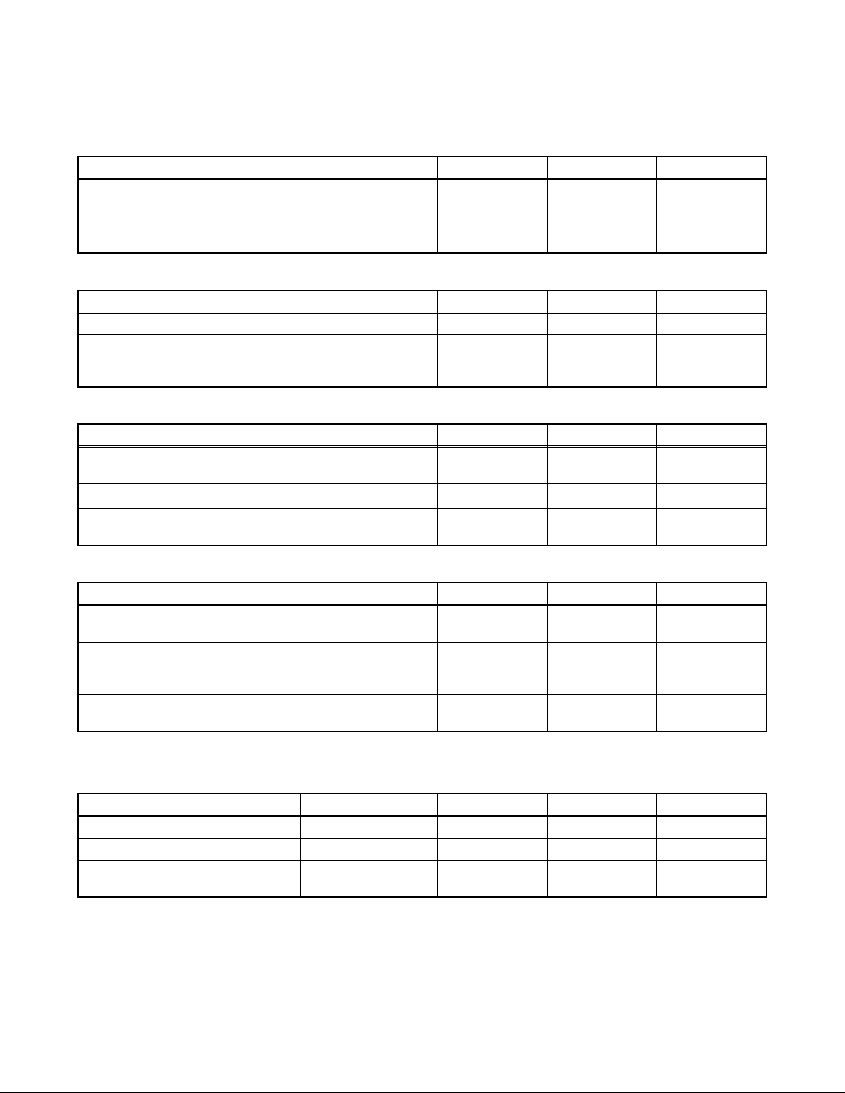
SPECIFICATIONS
< TUNER / NTSC >
ANT. Input ---------------------- 75 Ω Unbal., F type
Description Condition Unit Nominal Limit
1. AFT Pull-In Range --- MHz ±2.3 ±2.1
18
18
18
2. Synchronizing Sens.
TV.ch.4
CA.ch.31
CA.ch.87
dBμ
dBμ
dBμ
< TUNER / ATSC >
Description Condition Unit Nominal Limit
1. Received Freq. Range (-28dBm) --- kHz --- ±100
---
---
---
2. ATSC Dynamic Range (min / max)
ch.4
ch.10
ch.41
dBm
dBm
dBm
< LCD PANEL >
Description Condition Unit Nominal Limit
1. Native Pixel Resolution
2. Brightness (w / filter) ---
3. Viewing Angle
Horizontal
Vert ical
Horizontal
Vert ical
pixels
pixels
cd/m
°
°
1366
768
2
250 ---
-88 to 88
-88 to 88
20
20
23
-76/0
-76/0
-76/+4
---
---
---
---
< VIDEO >
Description Condition Unit Nominal Limit
1. Over Scan
2. Color Temperature
3. Resolution (composite video)
Horizontal
Vert ical
--x
y
Horizontal
Vert ical
%
%
°K 12000
line
line
5
5
0.272
0.278
400
350
5±5
5±5
--±3%
±3%
---
---
< AUDIO >
All items are measured across 8 Ω load at speaker output terminal with L.P.F.
Description Condition Unit Nominal Limit
1.
Audio MAX Output (ATSC 0dBfs)
2. Audio Distortion (NTSC) 500mW: Lch/Rch % 0.5/0.5 2.0/2.0
3. Audio Freq. Response (NTSC)
Lch/Rch W 8.0/8.0 7.0/7.0
-
6dB: Lch
-
6dB: Rch
Hz
Hz
70 to 10 k
70 to 10 k
100 to 8 k
100 to 8 k
1-1 PL12.6SP
Page 5
IMPORTANT SAFETY PRECAUTIONS
ALSO TEST WITH
PLUG REVERSED
USING AC
ADAPTER PLUG
AS REQUIRED
TEST ALL EXPOSED
METAL SURFACES
READING SHOULD
NOT BE ABOVE 0.5 mA
EARTH
GROUND
_
DEVICE
LEAKAGE
CURRENT
TESTER
+
BEING
TESTED
Prior to shipment from the factory, our products are strictly inspected for recognized product safety and electrical
codes of the countries in which they are to be sold. However, in order to maintain such compliance, it is equally
important to implement the following precautions when a set is being serviced.
Safety Precautions for LCD TV
Circuit
1. Before returning an instrument to the
customer, always make a safety check of the
entire instrument, including, but not limited to, the
following items:
a. Be sure that no built-in protective devices are
defective and have been defeated during
servicing. (1) Protective shields are provided
on this chassis to protect both the technician
and the customer. Correctly replace all missing
protective shields, including any removed for
servicing convenience. (2) When reinstalling
the chassis and/or other assembly in the
cabinet, be sure to put back in place all
protective devices, including but not limited to,
nonmetallic control knobs, insulating
fishpapers, adjustment and compartment
covers/shields, and isolation resistor/capacitor
networks. Do not operate this instrument or
permit it to be operated without all
protective devices correctly installed and
functioning. Servicers who defeat safety
features or fail to perform safety checks
may be liable for any resulting damage.
b. Be sure that there are no cabinet openings
through which an adult or child might be able to
insert their fingers and contact a hazardous
voltage. Such openings include, but are not
limited to, (1) spacing between the Liquid
Crystal Panel and the cabinet mask, (2)
excessively wide cabinet ventilation slots, and
(3) an improperly fitted and/or incorrectly
secured cabinet back cover.
c. Antenna Cold Check - With the instrument AC
plug removed from any AC source, connect an
electrical jumper across the two AC plug
prongs. Place the instrument AC switch in the
on position. Connect one lead of an ohmmeter
to the AC plug prongs tied together and touch
the other ohmmeter lead in turn to each tuner
antenna input exposed terminal screw and, if
applicable, to the coaxial connector. If the
measured resistance is less than 1.0 megohm
or greater than 5.2 megohm, an abnormality
exists that must be corrected before the
instrument is returned to the customer. Repeat
this test with the instrument AC switch in the off
position.
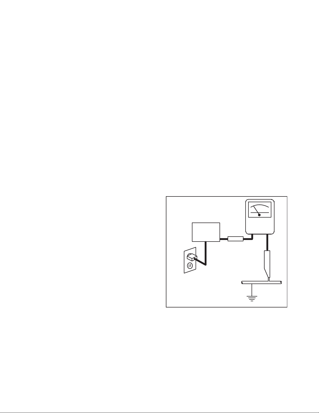
d. Leakage Current Hot Check - With the
instrument completely reassembled, plug the
AC line cord directly into a 120 V AC outlet. (Do
not use an isolation transformer during this
test.) Use a leakage current tester or a
metering system that complies with American
National Standards Institute (ANSI) C101.1
Leakage Current for Appliances and
Underwriters Laboratories (UL) 1410, (50.7).
With the instrument AC switch first in the on
position and then in the off position, measure
from a known earth ground (metal water pipe,
conduit, etc.) to all exposed metal parts of the
instrument (antennas, handle brackets, metal
cabinet, screw heads, metallic overlays, control
shafts, etc.), especially any exposed metal
parts that offer an electrical return path to the
chassis. Any current measured must not
exceed 0.5 milli-ampere. Reverse the
instrument power cord plug in the outlet and
repeat the test.
ANY MEASUREMENTS NOT WITHIN THE
LIMITS SPECIFIED HEREIN INDICATE A
POTENTIAL SHOCK HAZARD THAT MUST
BE ELIMINATED BEFORE RETURNING THE
2. Read and comply with all caution and safety-
2-1 LTVN_ISP
INSTRUMENT TO THE CUSTOMER OR
BEFORE CONNECTING THE ANTENNA OR
ACCESSORIES.
related notes on or inside the receiver cabinet, on
the receiver chassis, or on the Liquid Crystal
Panel.
Page 6

3. Design Alteration Warning - Do not alter or add
to the mechanical or electrical design of this TV
receiver. Design alterations and additions,
including, but not limited to circuit modifications
and the addition of items such as auxiliary audio
and/or video output connections, might alter the
safety characteristics of this receiver and create a
hazard to the user. Any design alterations or
additions will void the manufacturer's warranty and
may make you, the servicer, responsible for
personal injury or property damage resulting
therefrom.
4. Hot Chassis Warning a. Some TV receiver chassis are electrically
connected directly to one conductor of the AC
power cord and maybe safety-serviced without
an isolation transformer only if the AC power
plug is inserted so that the chassis is
connected to the ground side of the AC power
source. To confirm that the AC power plug is
inserted correctly, with an AC voltmeter,
measure between the chassis and a known
earth ground. If a voltage reading in excess of
1.0 V is obtained, remove and reinsert the AC
power plug in the opposite polarity and again
measure the voltage potential between the
chassis and a known earth ground.
b. Some TV receiver chassis normally have 85V
AC(RMS) between chassis and earth ground
regardless of the AC plug polarity. This chassis
can be safety-serviced only with an isolation
transformer inserted in the power line between
the receiver and the AC power source, for both
personnel and test equipment protection.
c. Some TV receiver chassis have a secondary
ground system in addition to the main chassis
ground. This secondary ground system is not
isolated from the AC power line. The two
ground systems are electrically separated by
insulation material that must not be defeated or
altered.
5. Observe original lead dress. Take extra care to
assure correct lead dress in the following areas: a.
near sharp edges, b. near thermally hot parts-be
sure that leads and components do not touch
thermally hot parts, c. the AC supply, d. high
voltage, and, e. antenna wiring. Always inspect in
all areas for pinched, out of place, or frayed wiring.
Check AC power cord for damage.
6. Components, parts, and/or wiring that appear to
have overheated or are otherwise damaged
should be replaced with components, parts, or
wiring that meet original specifications.
Additionally, determine the cause of overheating
and/or damage and, if necessary, take corrective
action to remove any potential safety hazard.
7. Product Safety Notice - Some electrical and
mechanical parts have special safety-related
characteristics which are often not evident from
visual inspection, nor can the protection they give
necessarily be obtained by replacing them with
components rated for higher voltage, wattage, etc.
Parts that have special safety characteristics are
identified by a # on schematics and in parts lists.
Use of a substitute replacement that does not
have the same safety characteristics as the
recommended replacement part might create
shock, fire, and/or other hazards. The product's
safety is under review continuously and new
instructions are issued whenever appropriate.
Prior to shipment from the factory, our products
are strictly inspected to confirm they comply with
the recognized product safety and electrical codes
of the countries in which they are to be sold.
However, in order to maintain such compliance, it
is equally important to implement the following
precautions when a set is being serviced.
2-2 LTVN_ISP
Page 7

Precautions during Servicing
A. Parts identified by the # symbol are critical for
safety.
Replace only with part number specified.
B. In addition to safety, other parts and assemblies
are specified for conformance with regulations
applying to spurious radiation. These must also be
replaced only with specified replacements.
Examples: RF converters, RF cables, noise
blocking capacitors, and noise blocking filters, etc.
C. Use specified internal wiring. Note especially:
1) Wires covered with PVC tubing
2) Double insulated wires
3) High voltage leads
D. Use specified insulating materials for hazardous
live parts. Note especially:
1) Insulation Tape
2) PVC tubing
3) Spacers
4) Insulators for transistors.
E. When replacing AC primary side components
(transformers, power cord, etc.), wrap ends of
wires securely about the terminals before
soldering.
F. Observe that the wires do not contact heat
producing parts (heat sinks, oxide metal film
resistors, fusible resistors, etc.)
G. Check that replaced wires do not contact sharp
edged or pointed parts.
H. When a power cord has been replaced, check that
11~13 lb (5~6 kg) of force in any direction will not
loosen it.
I. Also check areas surrounding repaired locations.
J. Use care that foreign objects (screws, solder
droplets, etc.) do not remain inside the set.
K. When connecting or disconnecting the internal
connectors, first, disconnect the AC plug from the
AC supply outlet.
L. When installing parts or assembling the cabinet
parts, be sure to use the proper screws and
tighten certainly.
2-3 LTVN_ISP
Page 8
Safety Check after Servicing
Examine the area surrounding the repaired location for damage or deterioration. Observe that screws, parts and
wires have been returned to original positions. Afterwards, perform the following tests and confirm the specified
values in order to verify compliance with safety standards.
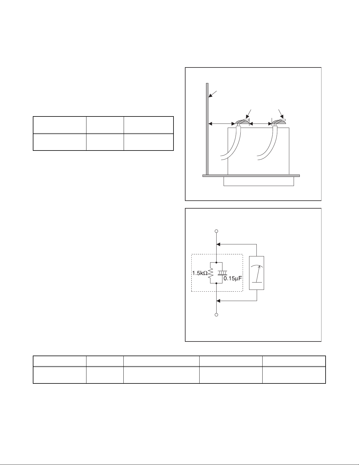
1. Clearance Distance
When replacing primary circuit components, confirm
specified clearance distance (d) and (d') between
soldered terminals, and between terminals and
surrounding metallic parts. (See Fig. 1)
Table 1: Ratings for selected area
Chassis or Secondary Conductor
Primary Circuit
AC Line Voltage Region
110 to 130 V
Note: This table is unofficial and for reference only. Be
sure to confirm the precise values.
U.S.A. or
Canada
Clearance
Distance (d), (d’)
≥ 3.2 mm
(0.126 inches)
2. Leakage Current Test
Confirm the specified (or lower) leakage current
between B (earth ground, power cord plug prongs) and
externally exposed accessible parts (RF terminals,
antenna terminals, video and audio input and output
terminals, microphone jacks, earphone jacks, etc.) is
lower than or equal to the specified value in the table
below.
Measuring Method: (Power ON)
Insert load Z between B (earth ground, power cord plug
prongs) and exposed accessible parts. Use an AC
voltmeter to measure across both terminals of load Z.
See Fig. 2 and following table.
d' d
Fig. 1
Exposed Accessible Part
Z
AC Voltmeter
(High Impedance)
Earth Ground
B
Power Cord Plug Prongs
Fig. 2
Table 2: Leakage current ratings for selected areas
AC Line Voltage Region Load Z Leakage Current (i) Earth Ground (B) to:
110 to 130 V
Note: This table is unofficial and for reference only. Be sure to confirm the precise values.
U.S.A. or
Canada
0.15 μF CAP. & 1.5 kΩ
RES. Connected in parallel
2-4 LTVN_ISP
i ≤ 0.5 mA rms
Exposed accessible
parts
Page 9
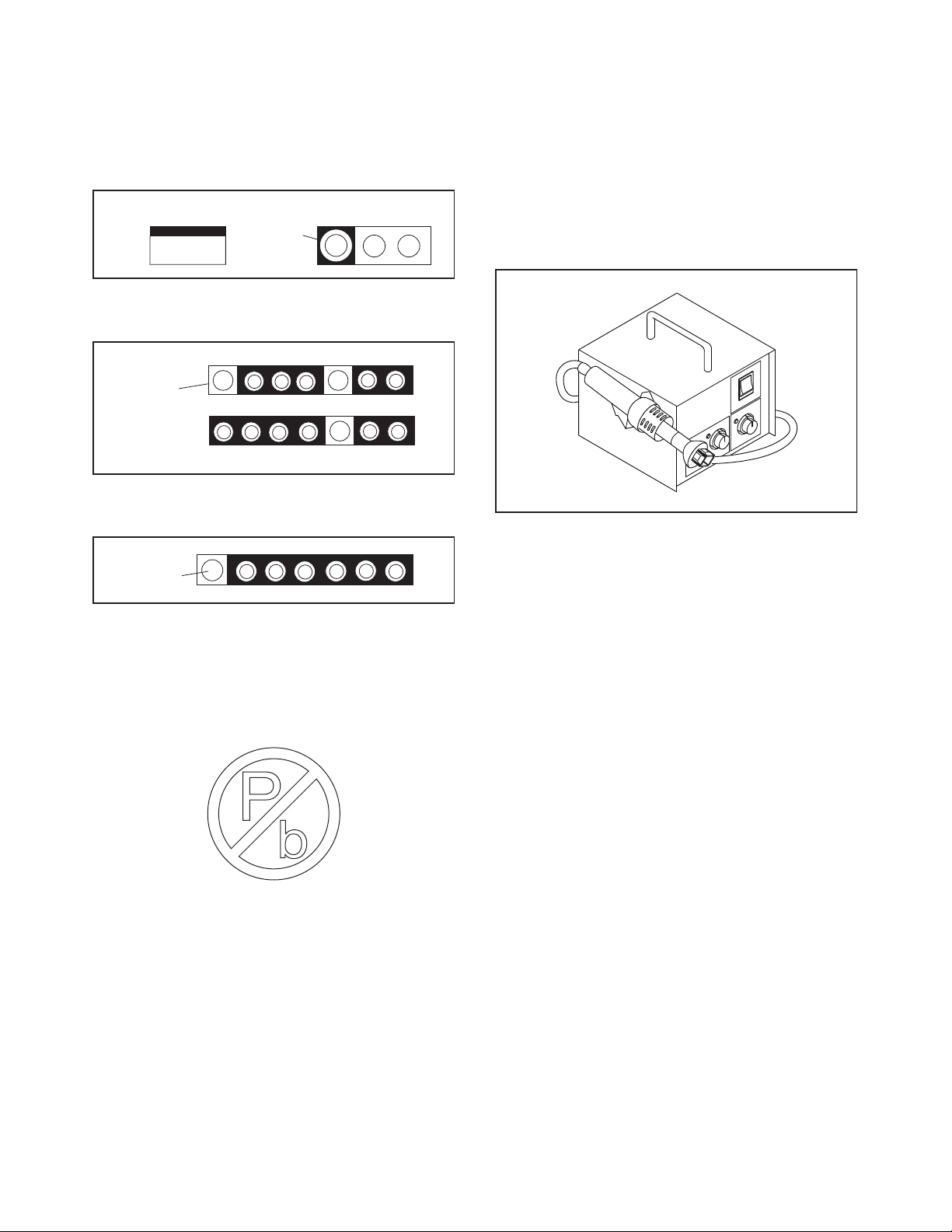
STANDARD NOTES FOR SERVICING
Top View
Out
In
Bottom View
Input
5
10
Pin 1
Pin 1
Fig. S-1-1
Circuit Board Indications
1. The output pin of the 3 pin Regulator ICs is
indicated as shown.
2. For other ICs, pin 1 and every fifth pin are
indicated as shown.
3. The 1st pin of every male connector is indicated as
shown.
Pb (Lead) Free Solder
Pb free mark will be found on PCBs which use Pb
free solder. (Refer to figure.) For PCBs with Pb free
mark, be sure to use Pb free solder. For PCBs
without Pb free mark, use standard solder.
Pb free mark
How to Remove / Install Flat Pack-IC
1. Removal
With Hot-Air Flat Pack-IC Desoldering Machine:
1. Prepare the hot-air flat pack-IC desoldering
machine, then apply hot air to the Flat Pack-IC
(about 5 to 6 seconds). (Fig. S-1-1)
2. Remove the flat pack-IC with tweezers while
applying the hot air.
3. Bottom of the flat pack-IC is fixed with glue to the
CBA; when removing entire flat pack-IC, first apply
soldering iron to center of the flat pack-IC and heat
up. Then remove (glue will be melted). (Fig. S-1-6)
4. Release the flat pack-IC from the CBA using
tweezers. (Fig. S-1-6)
CAUTION:
1. The Flat Pack-IC shape may differ by models. Use
an appropriate hot-air flat pack-IC desoldering
machine, whose shape matches that of the Flat
Pack-IC.
2. Do not supply hot air to the chip parts around the
flat pack-IC for over 6 seconds because damage
to the chip parts may occur. Put masking tape
around the flat pack-IC to protect other parts from
damage. (Fig. S-1-2)
3-1 TVN_SN
Page 10
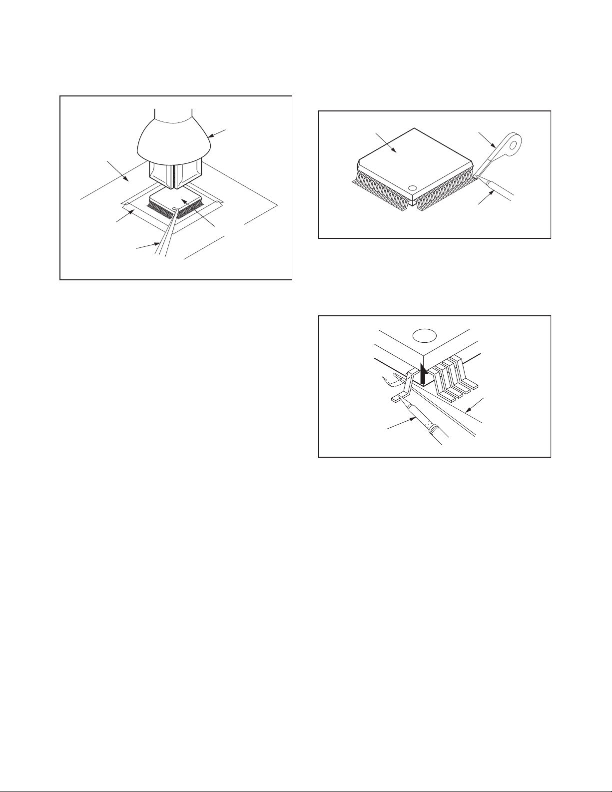
3. The flat pack-IC on the CBA is affixed with glue, so
Hot-air
Flat Pack-IC
Desoldering
Machine
CBA
Flat Pack-IC
Tweezers
Masking
Tape
Fig. S-1-2
Flat Pack-IC
Desoldering Braid
Soldering Iron
Fig. S-1-3
Fine Tip
Soldering Iron
Sharp
Pin
Fig. S-1-4
be careful not to break or damage the foil of each
pin or the solder lands under the IC when
removing it.
With Soldering Iron:
1. Using desoldering braid, remove the solder from
all pins of the flat pack-IC. When you use solder
flux which is applied to all pins of the flat pack-IC,
you can remove it easily. (Fig. S-1-3)
2. Lift each lead of the flat pack-IC upward one by
one, using a sharp pin or wire to which solder will
not adhere (iron wire). When heating the pins, use
a fine tip soldering iron or a hot air desoldering
machine. (Fig. S-1-4)
3. Bottom of the flat pack-IC is fixed with glue to the
CBA; when removing entire flat pack-IC, first apply
soldering iron to center of the flat pack-IC and heat
up. Then remove (glue will be melted). (Fig. S-1-6)
4. Release the flat pack-IC from the CBA using
tweezers. (Fig. S-1-6)
3-2 TVN_SN
Page 11
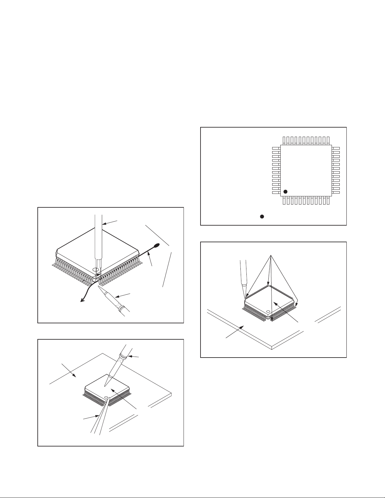
With Iron Wire:
To Solid
Mounting Point
Soldering Iron
Iron Wire
or
Hot Air Blower
Fig. S-1-5
Fine Tip
Soldering Iron
CBA
Flat Pack-IC
Tweezers
Fig. S-1-6
Example :
Pin 1 of the Flat Pack-IC
is indicated by a " " mark.
Fig. S-1-7
1. Using desoldering braid, remove the solder from
all pins of the flat pack-IC. When you use solder
flux which is applied to all pins of the flat pack-IC,
you can remove it easily. (Fig. S-1-3)
2. Affix the wire to a workbench or solid mounting
point, as shown in Fig. S-1-5.
3. While heating the pins using a fine tip soldering
iron or hot air blower, pull up the wire as the solder
melts so as to lift the IC leads from the CBA
contact pads as shown in Fig. S-1-5.
4. Bottom of the flat pack-IC is fixed with glue to the
CBA; when removing entire flat pack-IC, first apply
soldering iron to center of the flat pack-IC and heat
up. Then remove (glue will be melted). (Fig. S-1-6)
5. Release the flat pack-IC from the CBA using
tweezers. (Fig. S-1-6)
Note: When using a soldering iron, care must be
taken to ensure that the flat pack-IC is not
being held by glue. When the flat pack-IC is
removed from the CBA, handle it gently
because it may be damaged if force is applied.
2. Installation
1. Using desoldering braid, remove the solder from
the foil of each pin of the flat pack-IC on the CBA
so you can install a replacement flat pack-IC more
easily.
2. The “ I ” mark on the flat pack-IC indicates pin 1.
(See Fig. S-1-7.) Be sure this mark matches the
pin 1 on the PCB when positioning for installation.
Then presolder the four corners of the flat pack-IC.
(See Fig. S-1-8.)
3. Solder all pins of the flat pack-IC. Be sure that
none of the pins have solder bridges.
Presolder
Flat Pack-IC
CBA
Fig. S-1-8
3-3 TVN_SN
Page 12
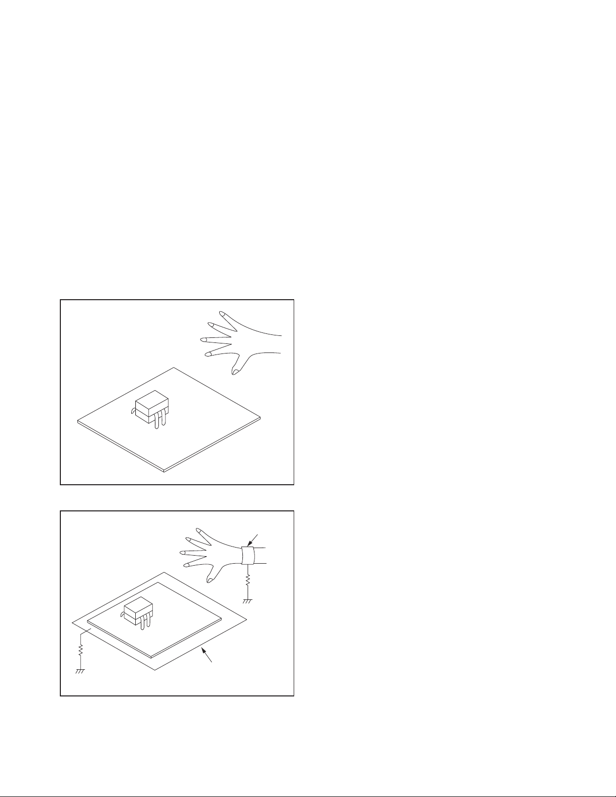
Instructions for Handling Semi-
<Incorrect>
CBA
Grounding Band
Conductive Sheet or
Copper Plate
1MΩ
1MΩ
<Correct>
CBA
conductors
Electrostatic breakdown of the semi-conductors may
occur due to a potential difference caused by
electrostatic charge during unpacking or repair work.
1. Ground for Human Body
Be sure to wear a grounding band (1 MΩ) that is
properly grounded to remove any static electricity that
may be charged on the body.
2. Ground for Workbench
Be sure to place a conductive sheet or copper plate
with proper grounding (1 MΩ) on the workbench or
other surface, where the semi-conductors are to be
placed. Because the static electricity charge on
clothing will not escape through the body grounding
band, be careful to avoid contacting semi-conductors
with your clothing.
3-4 TVN_SN
Page 13
CABINET DISASSEMBLY INSTRUCTIONS
[2] Stand
Assembly
[1] Rear Cover
[3] Power Supply
CBA
[5] Speaker
[6] Stand Holder
[9] Rear Frame
[4] Digital Main
CBA Unit
[7] Function
CBA
[10] LCD Module
[11] Front
Cabinet
[8] LCD Panel
Assembly
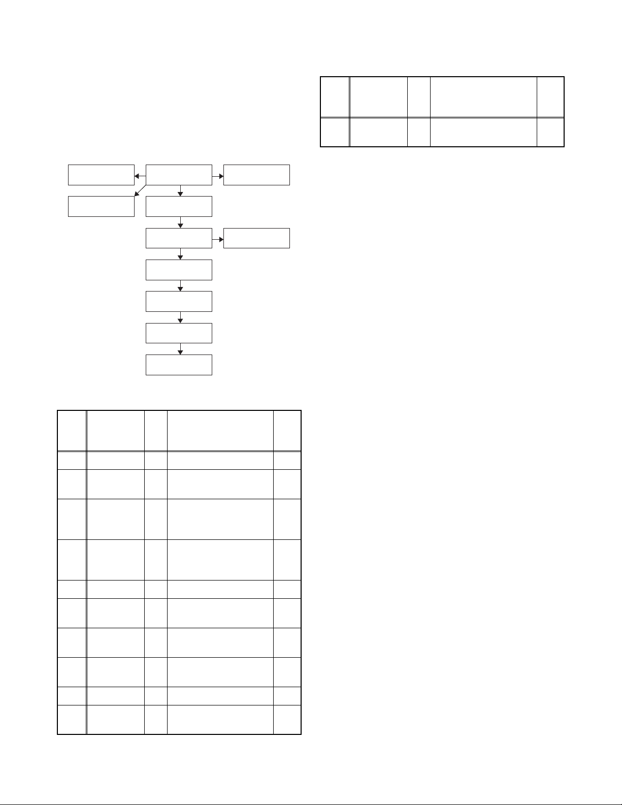
1. Disassembly Flowchart
This flowchart indicates the disassembly steps for the
cabinet parts and the CBA in order to gain access to
items to be serviced. When reassembling, follow the
steps in reverse order. Bend, route and dress the
cables as they were.
2. Disassembly Method
Step/
Loc.
No.
Part
Fig.
No.
Removal Note
[1] Rear Cover D1 6(S-1), 6(S-2) ---
Stand
[2]
Assembly
Power
[3]
Supply
CBA
Digital Main
[4]
CBA UnitD2D5
D1 3(S-3) ---
D2D55(S-4), CN601,
CN631, CN1001
4(S-5), CN3006,
CN3101, CN3801,
Jack Holder
[5] Speaker D3 --------------- ---
Stand
[6]
Holder
Function
[7]
CBA
LCD Panel
[8]
Assembly
[9] Rear Frame D4 12(S-7), 2(S-8) 1,3
LCD
[10]
Module
D3 2(S-6) ---
D3
Sensor Lens 2,3
D5
D3 --------------- 3
D4 --------------- 1,3
---
---
Step/
Loc.
No.
[11]
↓
(1)
Part
Front
Cabinet
↓
(2)
Fig.
No.
Removal Note
D4 --------------- 3
↓
(3)
↓
(4)
↓
(5)
Note:
(1) Order of steps in procedure. When reassembling,
follow the steps in reverse order. These numbers
are also used as the Identification (location) No. of
parts in figures.
(2) Parts to be removed or installed.
(3) Fig. No. showing procedure of part location
(4) Identification of parts to be removed, unhooked,
unlocked, released, unplugged, unclamped, or
desoldered.
P = Spring, L = Locking Tab, S = Screw,
H = Hex Screw, CN = Connector
e.g. 2(S-2) = two Screws of (S-2),
2(L-2) = two Locking Tabs of (L-2)
(5) Refer to the following "Reference Notes in the
Ta bl e ."
Precautions concerning the LCD Panel
Assembly:
1. When you disassemble the LCD Panel
Assembly
• Be careful not to scratch the Reflection Sheet with
the edge of Rear Frame when disassembling/
re-assembling it.
• Be careful not to drop any plastic chip on the
Reflection Sheet when/after you remove the Screws.
• Prohibit to put any external pressure on the
Reflection Sheet because the scratch on the back of
the Reflection Sheet have direct repercussion on the
display screen.
• Prohibit to put any external pressure on the Sheet
Holder or LED Heat Sink Assembly either because it
also has repercussion on the display screen via the
Reflection Sheet.
• You need to remove any visible dust from the
Reflection Sheet which creates the external
pressure between the Reflection Sheet and the
Sheet Holder/LED Heat Sink Assembly as a result.
• To prevent the Screw from being stripped, the screw
tightening torque should be 13.23 lbf·in(6 kgf·cm) for
the Rear Frame Screw and 5.512 lbf·in(2.5 kgf·cm)
for the LED Heat Sink Assembly Screw.
• Do not pull the FFC Cable and Board Cable
forcefully when you re-assemble.
4-1 PL12.6-A_DC
Page 14
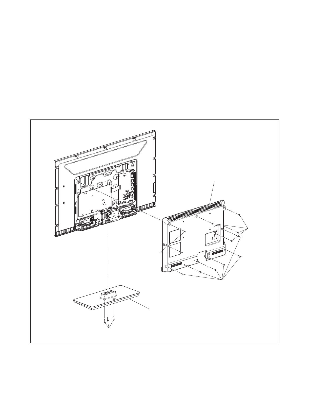
2. When you disassemble/re-assemble the
[1] Rear Cover
(S-3)
[2] Stand Assembly
(S-2)
(S-1)
(S-1)
Fig. D1
Function CBA on the Front Cabinet
• Detach the Function CBA, which is attached on the
Front Cabinet with double-sided tape, without
breaking it.
• When you put the Function CBA back on the New
Front Cabinet, you need to use specified new
double-sided tape and put the Function CBA onto
the New Front Cabinet with equal pressure to the
Board. (The gap more than 0.015 inch (0.4 mm)
between the Front Cabinet and Function CBA will
impair the sensor sensitivity.)
• Prepare for substitutional Function CBA in case you
break it when you detach it from the Front Cabinet.
3. Performance Test after reassembling the LCD
Panel Assembly
• After you swap any of the Front Cabinet, Rear Frame
or Function CBA, you need to make sure that there
is no Gomikami/Black Spot with foreign material or
Mura/White Spot on the display screen.
• Make sure there is no malfunction on the display
screen by checking the White Mode and White 20%
Mode in the Purity Check Mode.
• Check the operational sensitivity on Touch Sensor
Control Panel to make sure everything functions
normally.
4-2 PL12.6-A_DC
Page 15
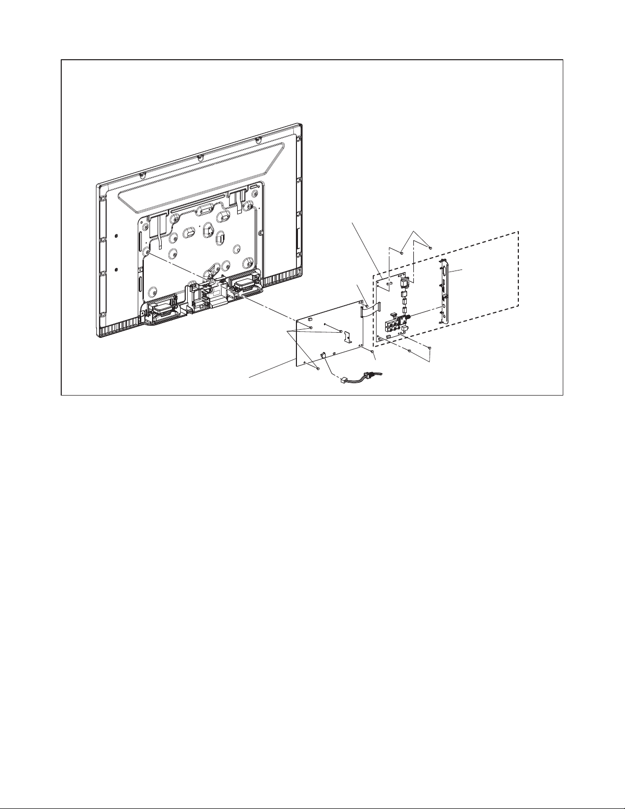
[3] Power Supply CBA
[4] Digital Main CBA Unit
(S-4)
(S-4)
(S-4)
(S-5)
(S-5)
Jack Holder
Fig. D2
4-3 PL12.6-A_DC
Page 16
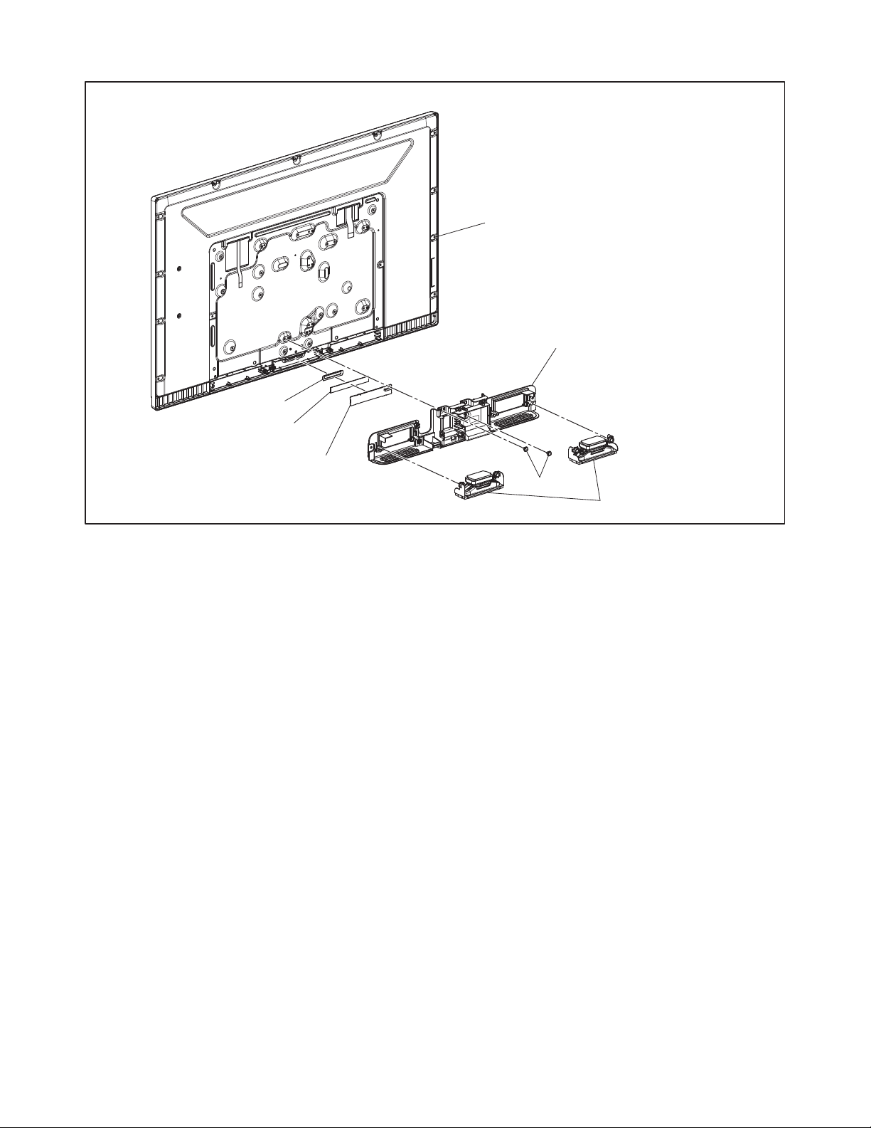
[6] Stand Holder
[7] Function CBA
*
1
[8] LCD Panel Assembly
*
1
[5] Speaker
(S-6)
Sensor Lens
Double-sided tape
Fig. D3
*1: Make sure to read all the precautions on page 4-1, 4-2 when you disassemble/re-assemble
the LCD Panel Assembly.
4-4 PL12.6-A_DC
Page 17

[9] Rear Frame
*
1
(S-7)
(S-7)
[10] LCD Module
*
1
(S-7)
(S-7)
(S-7)
(S-7)
(S-7)
(S-8)
Sheet Holder
Sheet Holder
LED Heat Sink Assembly
Reflection Sheet
FFC Cable
FFC Cable
[11] Front Cabinet
*
1
Fig. D4
*1: Make sure to read all the precautions on page 4-1, 4-2 when you disassemble/re-assemble
the LCD Panel Assembly.
4-5 PL12.6-A_DC
Page 18
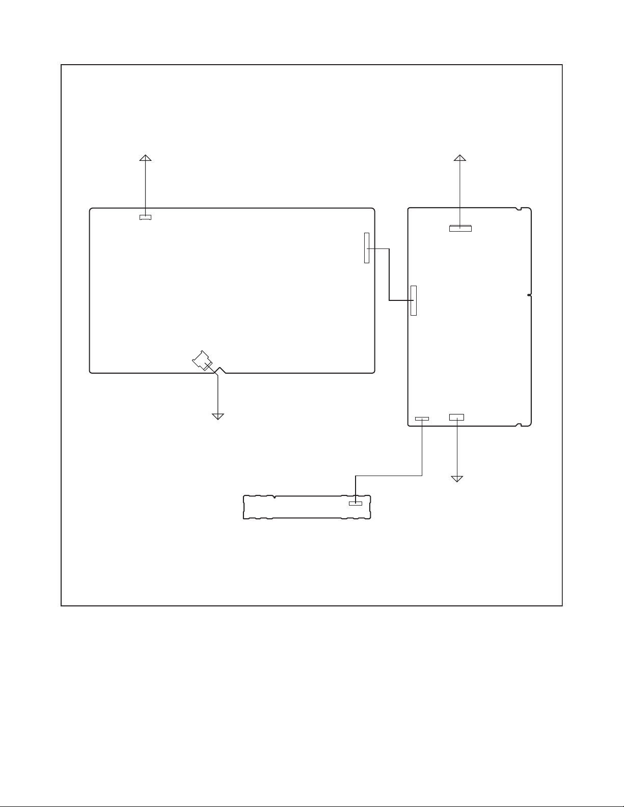
TV Cable Wiring Diagram
Power Supply CBA
Function CBA
To LCD Panel
Assembly
To LCD Panel
Assembly
To AC Cord
To Speaker
Digital Main
CBA Unit
CN3801
CN4001
CN1001
CN601
CN631
CN3006
CN3101
CN3701
Fig. D5
4-6 PL12.6-A_DC
Page 19

ELECTRICAL ADJUSTMENT INSTRUCTIONS
Code:
Pic code:
Panel-Option code:
MIPS:
Press "POWER" key to exit.
Safety:
HDMI EDID:
HDMI UART:
Touch Sensor Ver:
Safety_Non
**
OFF
-.-- / ---
Total Watch Time:
Lightsensor:
*****
**
"*" differs depending on the models.
*******-**-**-****-**
***-*****-***-***-*-**
**-***-***-***-***
Push 0 key
General Note: “CBA” is abbreviation for
“Circuit Board Assembly.”
Note: Electrical adjustments are required after
replacing circuit components and certain
mechanical parts. It is important to perform
these adjustments only after all repairs and
replacements have been completed.
Also, do not attempt these adjustments unless
the proper equipment is available.
Test Equipment Required
1. Remote control unit
2. Color Analyzer,
CA-310 (KONICA MINOLTA Luminance meter) or
measuring instrument as good as CA-310.
How to set up the service mode:
Service mode:
1. Turn the power on.
2. Press [MENU] button to display Setup menu.
3. Select “Features”.
4. Select “Software Upgrade”.
5. Select “Current Software Info”.
6. Press [0], [6], [2], [5], [9], [6] and [INFO] buttons on
the remote control unit in this order. The following
screen appears.
5-1 PL12.6(LC10)EA
Page 20
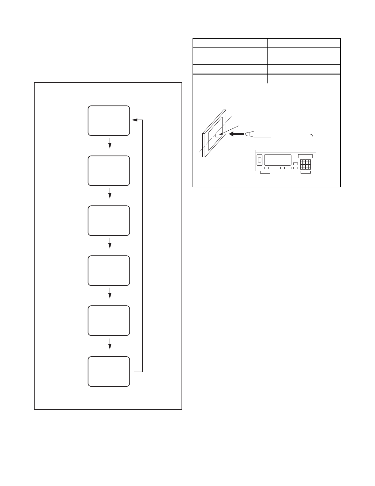
1. Purity Check Mode
[7] button
Note:
When entering this mode, the default setting is White mode.
Purity Check Mode
[7] button
White 50% mode
Red, Green, Blue mode
V-ramp mode
Black mode
[7] button
White mode
[7] button
[7] button
White 20% mode
[7] button
Color Analyzer
To avoid interference from ambient
light, this adjustment should be
performed in a dark room.
Perpendicularity
2. VCOM Adjustment
This mode cycles through full-screen displays of red,
green, blue, and white to check for non-active pixels.
1. Enter the service mode.
2. Each time the [7] button on the remote control unit
is pressed, the display changes as follows.
Test Point Adj. Point
Screen
[CHANNEL UP/DOWN]
buttons
M. EQ. Spec.
Color analyzer See below
Figure
1. Set the color analyzer at the zero point calibration
and bring the optical receptor pointing at the
center of the LCD-Panel.
Note: The optical receptor must be set
perpendicularly to the LCD Panel surface.
2. Enter the service mode.
3. Press [2] button on the remote control unit.
4. Press [CHANNEL UP/DOWN] buttons on the
remote control unit so that the color analyzer value
becomes minimum.
5. To cancel or to exit from the VCOM Adjustment,
press [CH RETURN] or [PREV CH] button.
3. To cancel or to exit from the Purity Check Mode,
press [CH RETURN] or [PREV CH] button.
Note:
Execute the VCOM adjustment within 2 minutes after
you turn the power on.
5-2 PL12.6(LC10)EA
Page 21
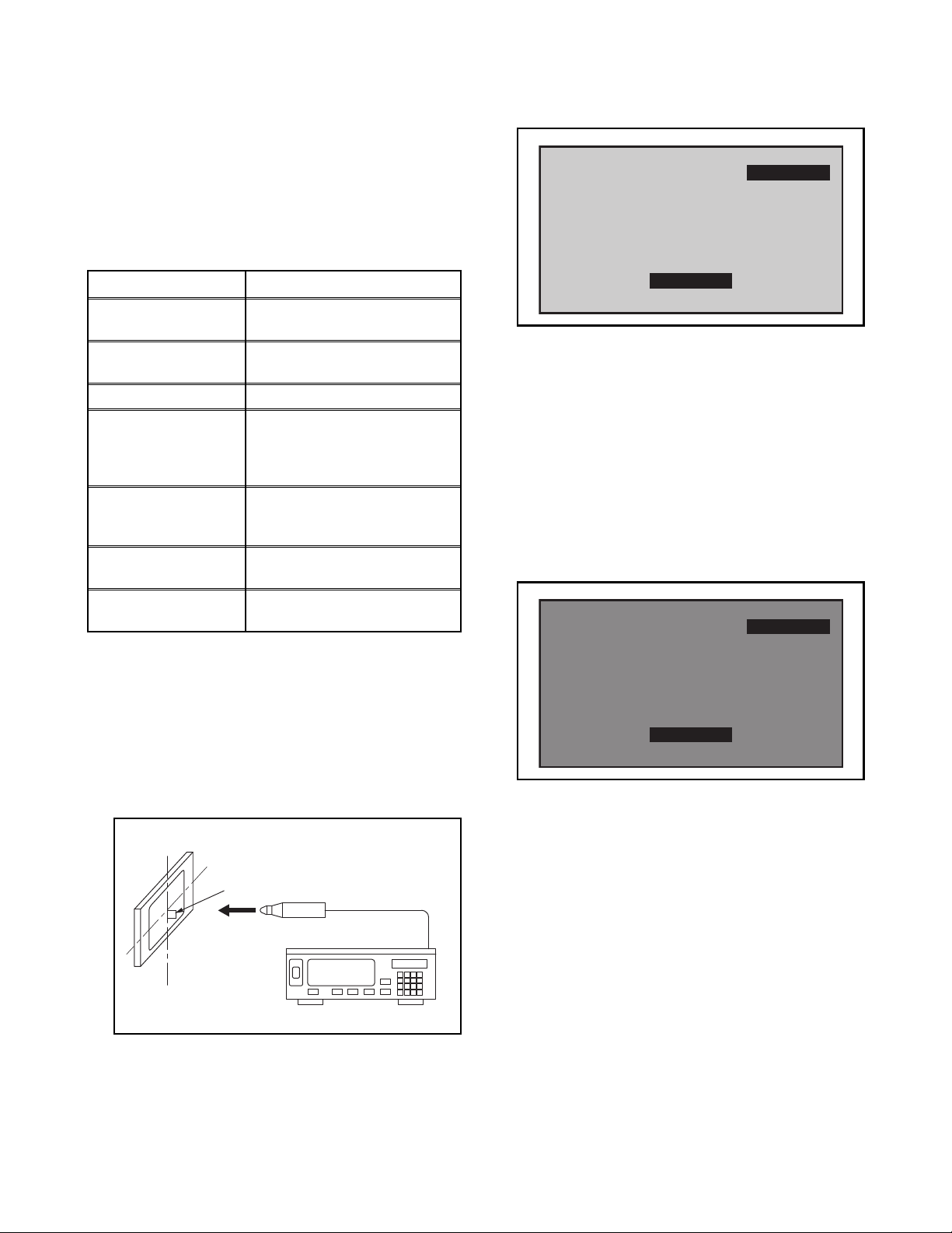
The White Balance Adjustment should be
Color Analyzer
Perpendicularity
To avoid interference from ambient
light, this adjustment should be
performed in a dark room.
Internal (Single)
HDB 0
Internal (Single)
LDB 0
performed when replacing the LCD Panel
or Digital Main CBA.
3. White Balance Adjustment
Purpose: To mix red and blue beams correctly for
pure white.
Symptom of Misadjustment: White becomes bluish
or reddish.
6. Press [MENU] button. The internal Raster signal
appears in the screen. (“Internal (Single)” appears
in the upper right of the screen as shown below.)
ITEM
Color temperature
Input Signal
SPECIFICATION
x= 0.272 ± 0.002
y= 0.278 ± 0.002
Internal pattern
(40/80% raster)
Measurement point Screen center
CA-310 (KONICA MINOLTA
M. EQ.
Luminance meter) or
measuring instrument as
good as CA-310.
60min.
Aging time
(Retail MODE/100IRE Raster
HDMI 1080i@60)
MODE setting of TV
Ambient
temperature
Shipment setting/
Retail MODE
25°C ± 5°C
1. Operate the unit for more than 60 minutes.
2. Enter the service mode.
3. Press [VOLUME DOWN] button three times on the
remote control unit to select “Drive setting” mode.
“Drive” appears in the screen.
4. Set the color analyzer at the CHROMA mode and
zero point calibration. Bring the optical receptor
pointing at the center of the LCD-Panel.
Note: The optical receptor must be set
perpendicularly to the LCD Panel surface.
5. Press [3] button to select the “HDB” for High Drive
Blue adjustment. (“HDB” appears in the screen.)
7. Press [CHANNEL UP/DOWN] buttons to adjust
the color temperature becomes 12000°K
=
0.272 / y= 0.278 ± 0.002).
(x
8. Press [1] button to select the “HDR” for High Drive
Red adjustment (“HDR” appears in the screen.)
and press [CHANNEL UP/DOWN] buttons to
adjust the color temperature.
9. If necessary, adjust the “HDB” or “HDR” again.
10. Press [6] button to select the “LDB” for Low Drive
Blue adjustment (“LDB” appears in the screen.)
and press [CHANNEL UP/DOWN] buttons to
adjust the color temperature.
11. Press [4] button to select the “LDR” for Low Drive
Red adjustment (“LDR” appears in the screen.)
and press [CHANNEL UP/DOWN] buttons to
adjust the color temperature.
12. If necessary, adjust the “LDB” or “LDR” again.
13. Press [VOLUME DOWN] button to shift to the
“Debugging Message” mode.
If there is no message under “[WB]” section, this
adjustment completes.
If “Drive settings are NG. Retry.” is displayed,
repeat above steps from 5. to 12. Then check
“Debugging Message” again. If “Drive settings are
NG. Retry.” is displayed, replace the LCD Panel or
Digital Main CBA.
14. To cancel or to exit from the White Balance
Adjustment, press [CH RETURN] or [PREV CH]
button.
5-3 PL12.6(LC10)EA
Page 22

HOW TO INITIALIZE THE LCD TV
The purpose of initialization is to place the set in a new out of box condition. The customer will be prompted to
select a language and program channels after the set has been initialized.
To put the program back at the factory-default, initialize the LCD TV using the following procedure.
NOTE: Disconnect any device from the USB Port
before you conduct on this procedure.
1. Turn the power on.
2. Enter the service mode.
- To cancel the service mode, press [POWER]
button on the remote control unit.
3. Press [BACK] button to enter the Panel Key
Confirmation Menu.
4. Press any button on the touch sensor panel.
5. Press [INFO] button to proceed with the self check
mode.
6. Make sure to confirm the “INITIALIZED FINISH”
appears in the green screen.
7. Unplug the AC Cord and plug it back on again.
6-1 PL12.6_INT
Page 23
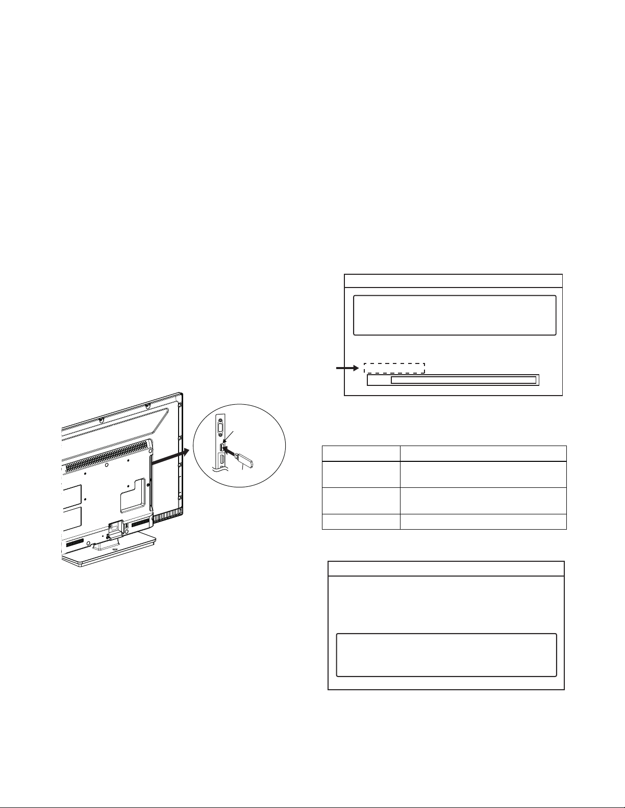
FIRMWARE RENEWAL MODE
USB port
USB storage
device
Rear Cabinet
Software upgrade in progress. Please wait.
Do not remove the USB storage device or
turn the TV off while upgrade is in progress.
Software Upgrade
Downloading...
Current Version:
New Version:
*******-***-*-***-****
*******-***-*-***-****
0%
*1
"*" differs depending on the models.
Software Upgrade
The software upgrade is completed.
Remove USB storage device, turn TV off then on again.
Equipment Required
a. USB storage device
b. Remote Control Unit
Firmware Update Procedure
User Upgrade (Filename example: TVNB012_00_UF_XX91_AA.ecc)
Upgrade the firmware only. The setting values will not be initialized.
The User Upgrade and the Firmware Upgrade (Factory Upgrade) will be done by the same file. If you want to
upgrade the firmware and initialize the setting values also, add “FACT_” at the beginning of the filename.
If you want to upgrade the firmware only and leave the setting values as they are, eliminate the “FACT_” from the
filename.
Update procedure
1. Turn the power on.
2. Press [MENU] button to display Menu.
3. Select “Features”.
4. Select “Software Upgrade”.
5. Select “Upgrade” to display Upgrade screen.
6. Press [OK] button to display Software Upgrade
screen.
7. Select “USB” and press [OK] button.
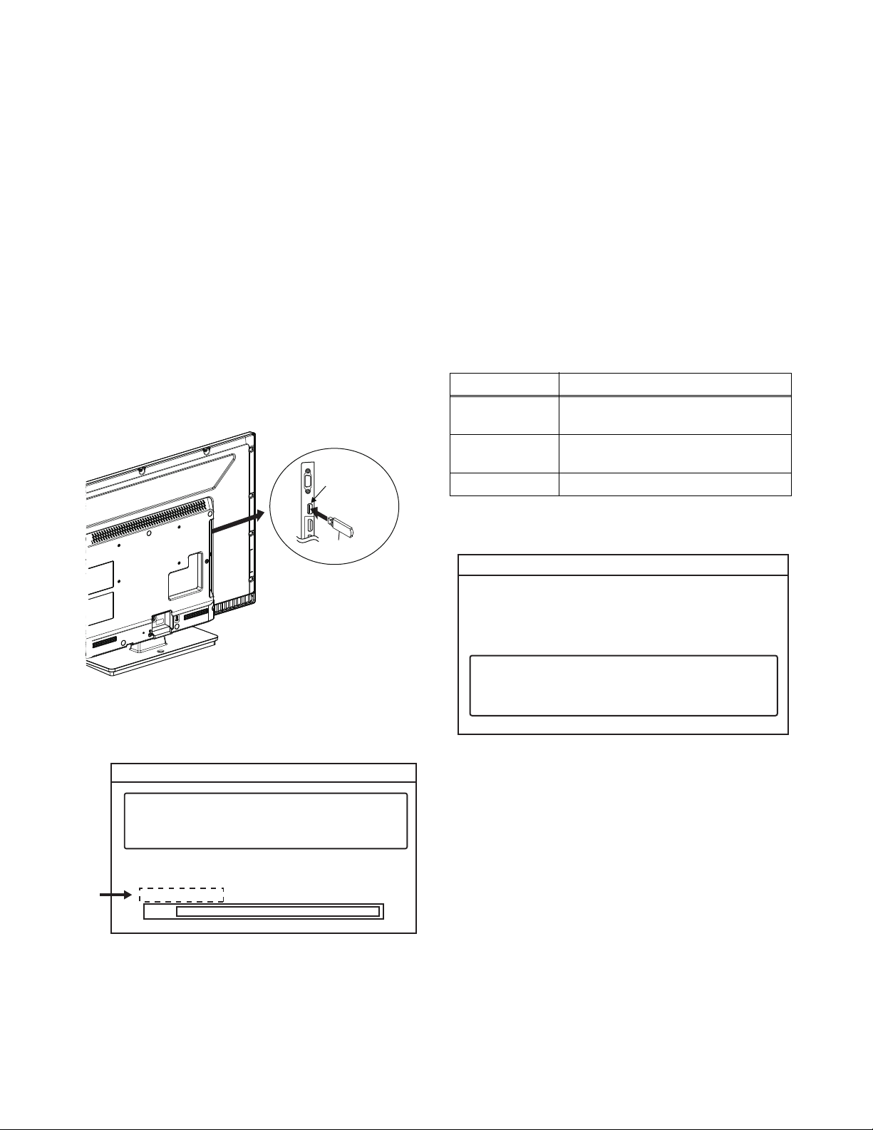
8. Insert the USB storage device to the USB port as
shown below.
11. The update will start and the following will appear
in the screen.
9. Select “Check” and press [OK] button.
10. Select “Upgrade” and press [OK] button to start
software upgrade.
Note: If the above screen isn’t displayed, repeat from
step 1.
The appearance shown in *1 is described as follows.
Appearance State
Downloading...
Writing...
Downloading the firmware from
the USB storage device.
Writing the downloaded firmware
in flash memory.
Checking... Checking the new firmware.
12. When the firmware update is completed, the
following will appear in the screen.
Remove the USB storage device from the USB
port.
Turn the power off and turn the power on again.
7-1 PL12.6FW
Page 24
Factory Upgrade (Firmware Upgrade/Flash Upgrade)
USB port
USB storage
device
Rear Cabinet
Software upgrade in progress. Please wait.
Do not remove the USB storage device or
turn the TV off while upgrade is in progress.
Software Upgrade
Downloading...
Current Version:
New Version:
*******-***-*-***-****
*******-***-*-***-****
0%
*1
"*" differs depending on the models.
Software Upgrade
The software upgrade is completed.
Remove USB storage device, turn TV off then on again.
Firmware Upgrade (Filename example: FACT_TVNB012_00_UF_XX91_AA.ecc)
Upgrade the firmware and initialize the setting values.
The User Upgrade and the Firmware Upgrade (Factory Upgrade) will be done by the same file. If you want to
upgrade the firmware and initialize the setting values also, add “FACT_” at the beginning of the filename.
If you want to upgrade the firmware only and leave the setting values as they are, eliminate the “FACT_” from the
filename.
Flash Upgrade (Filename example: ALL_TVNB012_00_UF_XX91_AA.ecc)
Upgrade the firmware and initialize the setting values along with the factory default such as White Balance, etc.
Before the upgrade, you will need to make a note of all the factory default so you will be able to set it back on the
TV after the initialization.
The Flash Upgrade will be done by it's unique file.
The User Upgrade/Firmware Upgrade (Factory Upgrade) file cannot be used for this upgrade.
Update procedure
1. Turn the power off.
2. Insert the USB storage device to the USB port as
shown below.
The appearance shown in *1 is described as follows.
Appearance State
Downloading...
Writing...
Downloading the firmware from
the USB storage device.
Writing the downloaded firmware
in flash memory.
Checking... Checking the new firmware.
3. Turn the power on.
4. The update will start and the following will appear
5. When the firmware update is completed, the
following will appear in the screen.
in the screen.
Remove the USB storage device from the USB
port.
Turn the power off and turn the power on again.
Service mode initial screen with a word
“INITIALIZED” will appear in the screen. The color
of the word “INITIALIZED” will change from red to
green when initialization is completed.
Note: If the above screen isn’t displayed, repeat from
step 1.
7-2 PL12.6FW
Page 25
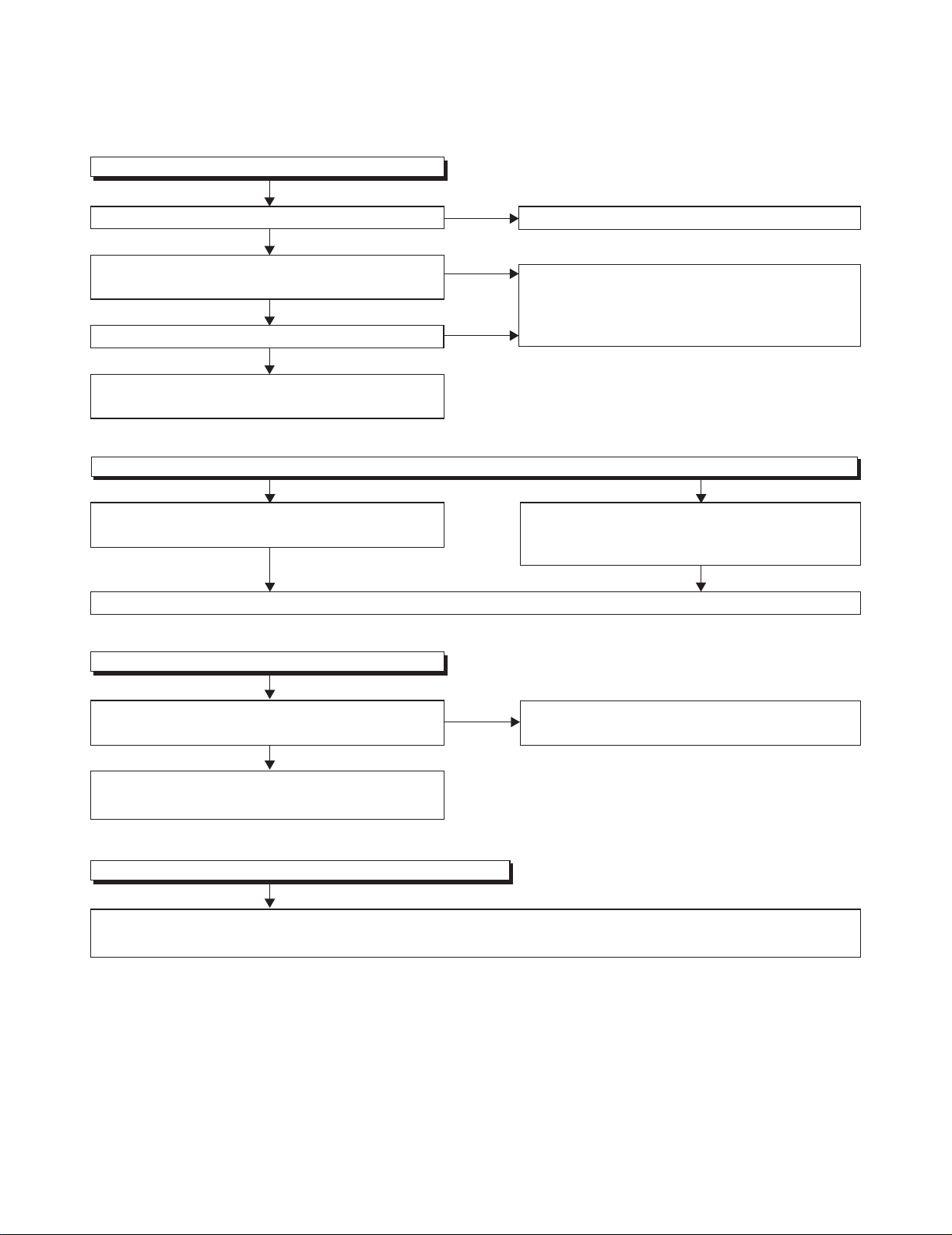
[Power Supply Section]
FLOW CHART NO.1
The power cannot be turned on.
TROUBLESHOOTING
Is the fuse (F601) normal?
Ye s
Is normal state restored when once unplugged
power cord is plugged again after several seconds?
Ye s
Is the P-ON+21V line voltage normal?
Ye s
Check each rectifying circuit of the secondary
circuit and repair it if defective.
FLOW CHART NO.2
The fuse blows out.
Check if there is any leak or short-circuit on the
primary circuit component and repair it if defective.
Make sure to repair the primary circuit component before replacing the fuse.
FLOW CHART NO.3
When the output voltage fluctuates.
No
No
No
See FLOW CHART No.2 <The fuse blows out.>
Check if there is any leak or short-circuit on the
primary circuit component and repair it if defective.
(D601, D602, D603, D604, Q601, Q602, T601)
Check if there is any leak or short-circuit on the
each rectifying circuit component of secondary side
and repair it if defective.
Does the photocoupler circuit on the secondary side
operate normally?
Ye s
Check IC601, D605, D607, D608, D609A, D610A, Q601,
Q602 and their periphery circuit. Repair it if defective.
FLOW CHART NO.4
When buzz sound can be heard in the periphery of power circuit.
Check if there is any short-circuit on the rectifying diode and the circuit in each rectifying circuit of the secondary side.
Repair it if defective. (D650, D651, D653, Q656)
No
Check IC601, D660, D661, Q652, Q653 and their
periphery circuit. Repair it if defective.
8-1 PL12.6ATR
Page 26
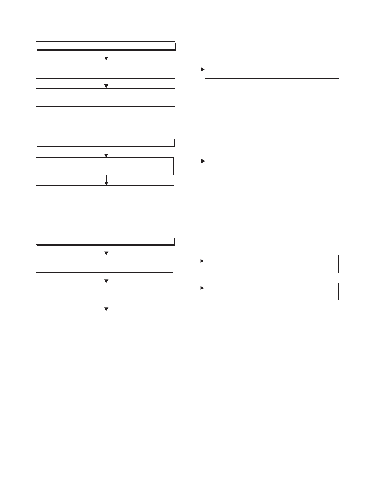
FLOW CHART NO.5
P-ON+21V is not output.
Is approximately +21V voltage supplied to the cathode
of D650(D651)?
Ye s
Check if there is any leak or short-circuit on the load
circuit. Repair it if defective.
FLOW CHART NO.6
AMP+24V is not output.
Is approximately +24V voltage supplied to the cathode
of D653?
Ye s
Check if there is any leak or short-circuit on the load
circuit. Repair it if defective.
FLOW CHART NO.7
AL+3.3V is not output.
No
No
Check D650, D651, C651, C652, C653 and their
periphery circuit. Repair it if defective.
Check D653, D654, C654, C655 and their periphery
circuit. Repair it if defective.
Is approximately +21V voltage supplied to the
collector of Q656?
Ye s
Is approximately +4V voltage supplied to the base of
Q656?
Ye s
Replace Q656.
No
No
Check D650, D651, C651, C652, C653 and their
periphery circuit. Repair it if defective.
Check D662 and their periphery circuit. Repair it if
defective.
8-2 PL12.6ATR
Page 27
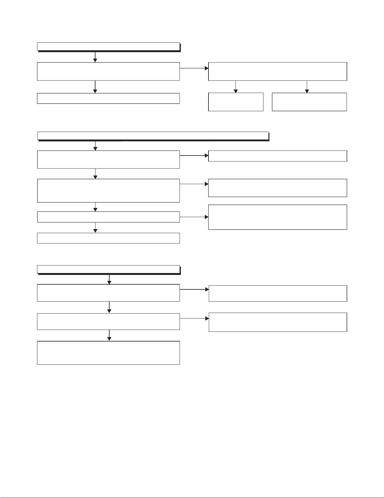
[Video Signal Section]
FLOW CHART NO.1
The key operation is not functioning.
When touching each buttons, does the Pin(6) voltage
of CN4001 decrease?
Ye s Ye s
Replace Digital Main CBA Unit. Replace IC4001
FLOW CHART NO.2
No operation is possible from the remote control unit. (Operation is possible from the unit.)
Is approximately +3.3V voltage supplied to Pin(3)
terminal of the remote control receiver (RS4051)?
Ye s
Is the "L" pulse supplied to Pin(1) terminal of remote
control receiver (RS4051) when the infrared remote
control is activated?
Ye s
Is the "L" pulse supplied to Pin(5) of CN4001?
Ye s
Replace Digital Main CBA Unit.
No
No
No
No
Is approximately +3.3V voltage supplied to Pin(1)
of CN4001?
or Function CBA.
Check AL+3.3V line and repair it if defective.
Replace the remote control receiver (RS4051)
or the remote control unit.
Check the line between Pin(1) of remote control
receiver (RS4051) and Pin(5) of CN4001.
Repair it if defective.
No
Check AL+3.3V line and
repair it if defective.
FLOW CHART NO.3
Picture does not appear normally.
Is approximately +21V voltage supplied to
Pin(16, 17, 22, 23) of CN631?
Ye s
Is
approximately +
CN631?
Digital Main CBA Unit or LCD Panel Assembly may
be defective.
Check and replace these parts.
3.3V voltage supplied to Pin(11) of
Ye s
No
No
See FLOW CHART NO.5 <P-ON+21V is not output.
[Power Supply Section]>
See FLOW CHART NO.7 <AL+3.3V is not output.
[Power Supply Section]>
8-3 PL12.6ATR
Page 28
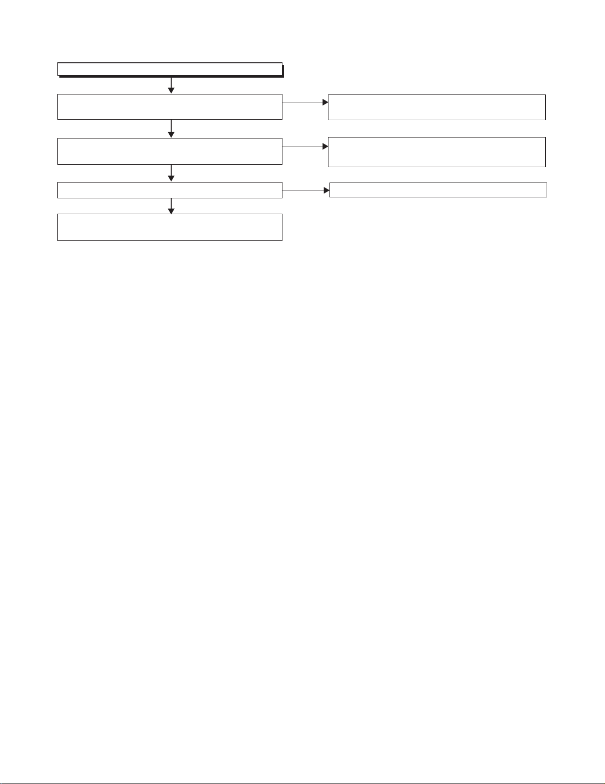
[Audio Signal Section]
FLOW CHART NO.1
Audio is not output normally.
Is approximately +24V voltage supplied to Pin(13, 14)
of CN631?
Ye s
approximately +
Is
CN631?
Are the audio signals output to Pin(1, 4) of CN3801?
SP3801, SP3802 or CL3801 may be defective.
Check and replace these parts.
3.3V voltage supplied to Pin(11) of
Ye s
Ye s
No
No
No
See FLOW CHART NO.6 <AMP+24V is not output.
[Power Supply Section]>
See FLOW CHART NO.7 <AL+3.3V is not output.
[Power Supply Section]>
Replace Digital Main CBA Unit.
8-4 PL12.6ATR
Page 29
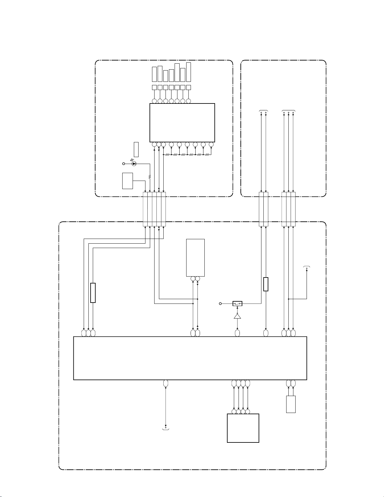
BLOCK DIAGRAMS
1. System Control Block Diagram
POWER
SOURCE
MENU
CH UP
CH DOWN
161718
19
212223
MENU
CH UP
POWER
SOURCE
CH DOWN
SCL
P-ON+5V
REMOTE
RS4051
D4051
POWER
SENSOR
SDA
IC4001
(TOUCH SENSOR)
4
5
POWER
1
MENU
SOURCE
3
2
VOL UP
VOL UP
VOL DOW N
VOL DOWN
CH UP
6
CH DOWN
11
TO
POWER SUPPLY
BLOCK DIAGRAM
RESET
P-ON-H2
FUNCTION CBA
VOL DOW N
VOL UP
13
12
CN631
TO
LED BACKLIGHT DRIVE
PROTECT3
BACKLIGHT-SW
CN631
BLOCK DIAGRAM
BACKLIGHT-ADJ
POWER SUPPLY CBA
IC3005
(MAIN MICRO CONTROLLER)
A15
KEY-IN1
LED DRIVE
D14
C14
LED1
REMOTE
Q3501, Q3502
KEY-IN146
SDA19
SCL28
REMOTE55
LED164
CN3101 CN4001
TU3901 (TUNER UNIT)
AUDIO-MUTE
C1
SCL
4
R12
SCL
SDA
3
T12
SDA
AL+3.3V
Q3006
B16
P-ON-H2
SCK
SIN
T11
P11
P-ON-H2
RESET
77
88
CN3701
IC3009
RESET
Q3005
RESET J15
SOUT
CS
P12
R11
PROTECT3
BACKLIGHT-SW
BACKLIGHT-ADJ
44
22
33
CN3701
TO
VIDEO/AUDIO
BLOCK DIAGRAM
BACKLIGHT-SW
F3BACKLIGHT-ADJ
B13
PROTECT3
BACKLIGHT-SW E2
DIGITAL MAIN CBA UNIT
XOUT25
XIN25
H15
H16
AUDIO-MUTE
TO
VIDEO/AUDIO
BLOCK DIAGRAM
9-1
25MHz
OSC
652
1
SI
CS
SO
SCK
IC3006 (MEMORY)
X3001
PL12.6ABLS
Page 30
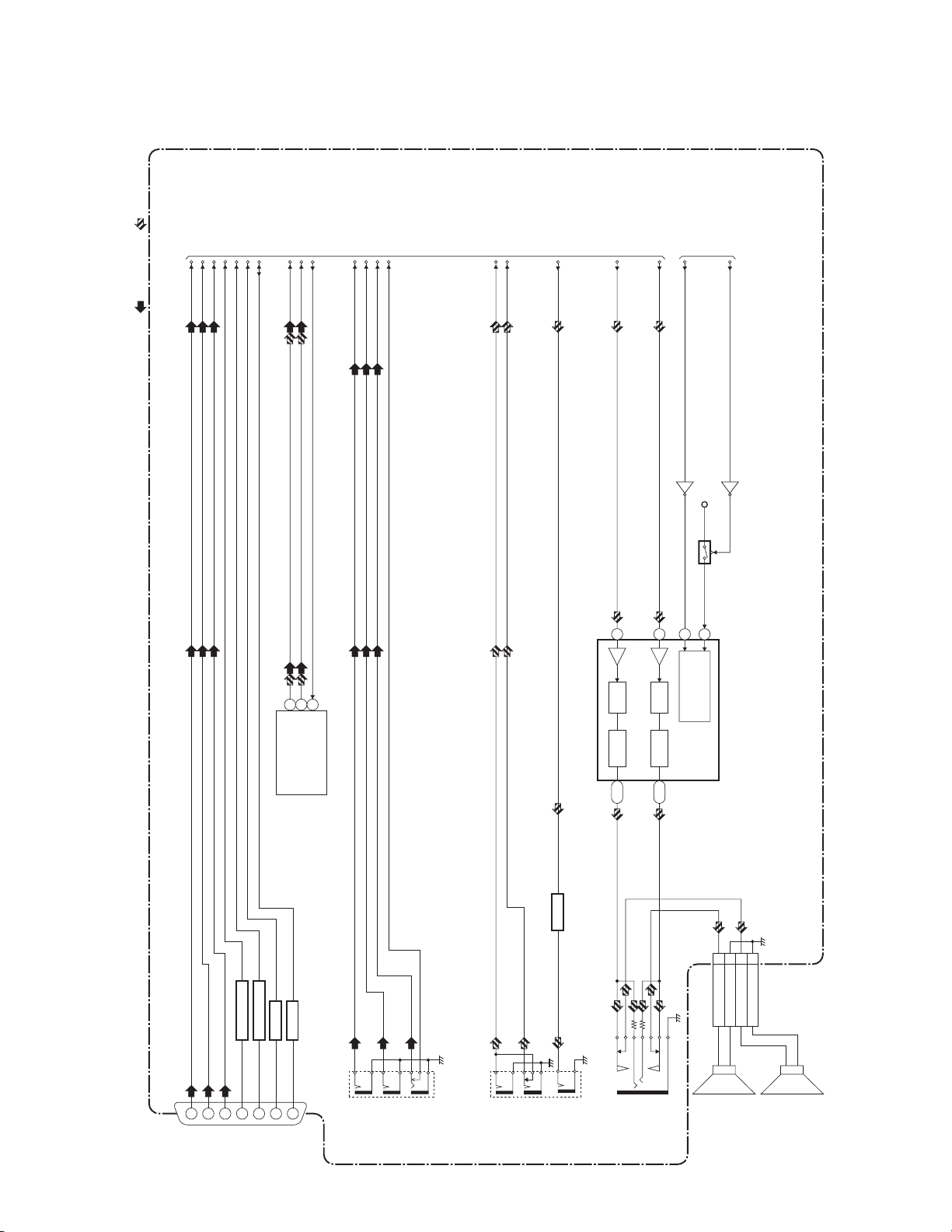
2. Video/Audio Block Diagram
AUDIO SIGNAL
TO DIGITAL
SIGNAL PROCESS
BLOCK DIAGRAM
TO SYSTEM CONTROL
BLOCK DIAGRAM
VIDEO SIGNAL
VGA-R-IN
VGA-G-IN
VGA-B-IN
VGA-HSYNC
VGA-SCL
VGA-VSYNC
VGA-SDA
(TUNER UNIT)
TU3901
IF-AGC
DIF-OUT1
DIF-OUT2
6
7
DIF-OUT2
DIF-OUT1
COM-VIDEO-Y/VIDEO-IN
5
IF-AGC
COMP-DET
COM-VIDEO-Pr-IN
COM-VIDEO-Pb-IN
AUDIO(L)-IN
AUDIO(R)-IN
SPDIF
AMP(R)-OUT
32
DRIVE PWM19DRIVE PWM
IC3801 (AUDIO AMP)
39,40
AMP(L)-OUT
AUDIO-MUTE
Q3801
34
11,12
BACKLIGHT-SW
Q3802
P-ON+5V
Q3803
DIGITAL MAIN CBA UNIT
17
CONTROL LOGIC
123
BUFFER GATE
IC3013
131415
JK3001
PC-RGB
IN
BUFFER GATE
IC3014
BUFFER
Q3301
BUFFER
Q3302
12
JK3702
COMPONENT
-Y/VIDEO-IN
COMPONENT
-Pb-IN
COMPONENT
-Pr-IN
9-2
JK3701
AUDIO(L)-IN
Q3701
AUDIO(R)-IN
BUFFER
DIGITAL
AUDIO-OUT
(COAXIAL)
JK3703
HEADPHONE
JACK
1
CN3801
SP(L)
SP3801
3
4
2
GND
GND
SP(R)
SPEAKER
L-CH
PL12.6ABLVA
SP3802
SPEAKER
R-CH
Page 31
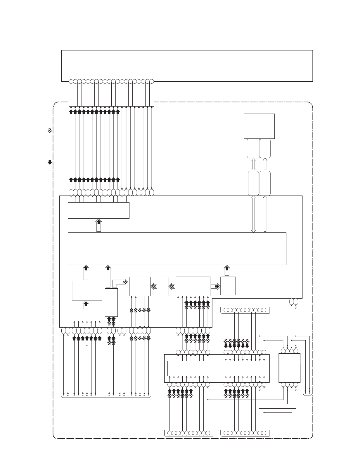
3. Digital Signal Process Block Diagram
LCD PANEL
ASSEMBLY
LLV0(+)23
LLV0(-)22
LLV1(+)21
LLV1(-)20
LLV2(+)19
LLV2(-)18
LLV3(+)13
LLV3(-)12
LLV4(+)11
LLV4(-)10
LLV5(+)9
LLV5(-)8
TP6
POL5
CPV4
OE3
STV1
M15
POL
L16
CPV
L15
OE
M14
STV
OE22
L14
OE2
CN3006
AUDIO SIGNAL
VIDEO SIGNAL
P14
P13
N16
N15
P16
P15
T16
T15
R14
T14
R13
T13
LLVCLK(+)16
R16
LLVCLK(-)15
R15
L13
TP
IC3002
(DDR2 SDRAM)
B1,B9,C2,C8,
D1,D3,D7,D9,
N4,N7,N8,P3,P4,
DATA(0-15)
ADDRESS(0-12)
H1,H3,H7,H9
F1,F9,G2,G8,
M2,M3,M7,M8,
N2,N3,N7,N8,
P2,P3,P7,P8,R2
P6-P8,R3,R4,R6,
R8,T2-T5
H1,H2,J1,J2,J4,K1,
K3,L1,L2,M1-M3,N1
HSYNC
IC3005 (DIGITAL SIGNAL PROCESS)
A14
VGA-HSYNC
VSYNC
B14
C11
VGA-R-IN
VGA-G-IN
VGA-VSYNC
LVDS TX
A/D
CONVERTER
SW
A9
C7
D8
C9
B11
C10
COM-VIDEO-Pr-IN
COM-VIDEO-Pb-IN
COM-VIDEO-Y/VIDEO-IN
VGA-B-IN
DEMODULATOR
/MPEG DECODER
IF-AGC
A12
A16
B12
DIF-OUT1
DIF-OUT2
IF-AGC
AUDIO I/F
COMP-DET
B7
A8
N12
N10
AMP(L)-OUT
SPDIF
COMP-DETB8AUDIO(R)-IN
AUDIO(L)-IN
A7
AMP(R)-OUT
DIGITAL
SIGNAL
PROCESS
AUDI O
DECODER
B4A4B3A3B2A2B1
26272324202117
IC3018 (HDMI SW)
414544484739383637
HDMI
DIGITAL MAIN CBA UNIT
I/F
A1
18
VIDEO
DECODER
79461
HDMI-IN3
JK3003
TMDS-D0(-)
TMDS-D0(+)
TMDS-D1(+)
575660596362545351
HDMI
SW
8
7
111014
3
TMDS-D1(-)
TMDS-D2(-)
TMDS-D2(+)
13
101216
15
HDMI-DATA
HDMI-CLOCK
TMDS-CLOCK(-)
TMDS-CLOCK(+)
52
541
2
IC3011
(HDMI SERIAL EEPROM)
15
SCL2
SCL1
2
HDMI-SCL
G14
7
14
SCL0
SDA2
SDA1
SCL3
3
10
HDMI-SDA
F14
6
SDA0
SDA3
11
VGA-SDA
VGA-SCL
TO
VIDEO/AUDIO
TO
VIDEO/AUDIO
BLOCK DIAGRAM
HDMI-IN1
JK3004
TMDS-D0(+)
TMDS-D0(-)
TMDS-D1(+)
7 42
94613
9-3
TMDS-D1(-)
TMDS-D2(+)
TMDS-D2(-)
TMDS-CLOCK(+)
TMDS-CLOCK(-)
HDMI-DATA
HDMI-CLOCK
101216
TMDS-D0(+)
TMDS-D0(-)
TMDS-D1(+)
TMDS-D1(-)
TMDS-D2(+)
TMDS-D2(-)
TMDS-CLOCK(+)
TMDS-CLOCK(-)
HDMI-DATA
JK3002
HDMI-IN2
79461
15
3
101216
HDMI-CLOCK
15
PL12.6ABLD
BLOCK DIAGRAM
Page 32
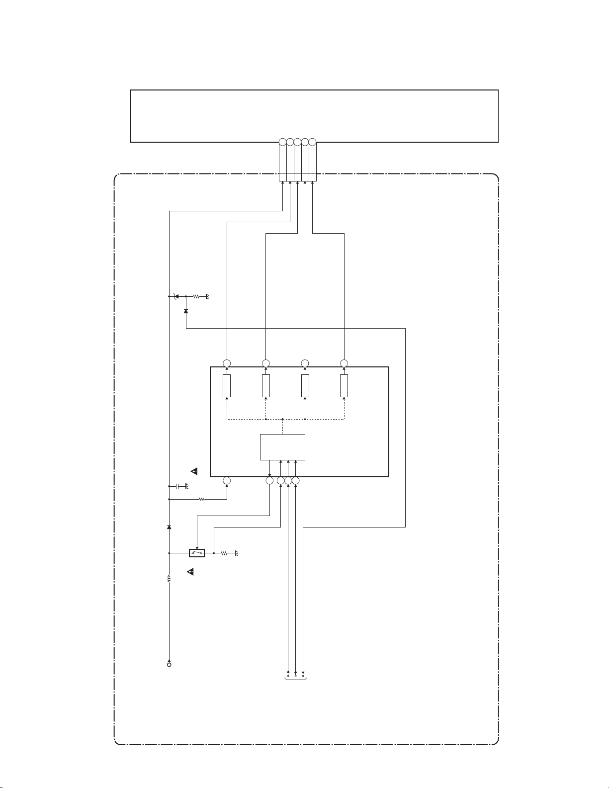
4. LED Backlight Drive Block Diagram
LCD PANEL
ASSEMBLY
ILED16
VLED4
ILED27
ILED32
ILED41
CN1001
2
DRIVE
OVP
IC1001
(LED BACKLIGHT DRIVER)
10
Q1001
DRIVE 3
161413
CONTROL
LOGIC
1
4
DRIVE 5
DRIVE
POWER SUPPLY CBA
P-ON+21V
BACKLIGHT-ADJ
BACKLIGHT-SW
PROTECT3
TO
SYSTEM CONTROL
BLOCK DIAGRAM
9-4
PL12.6BLBD
Page 33
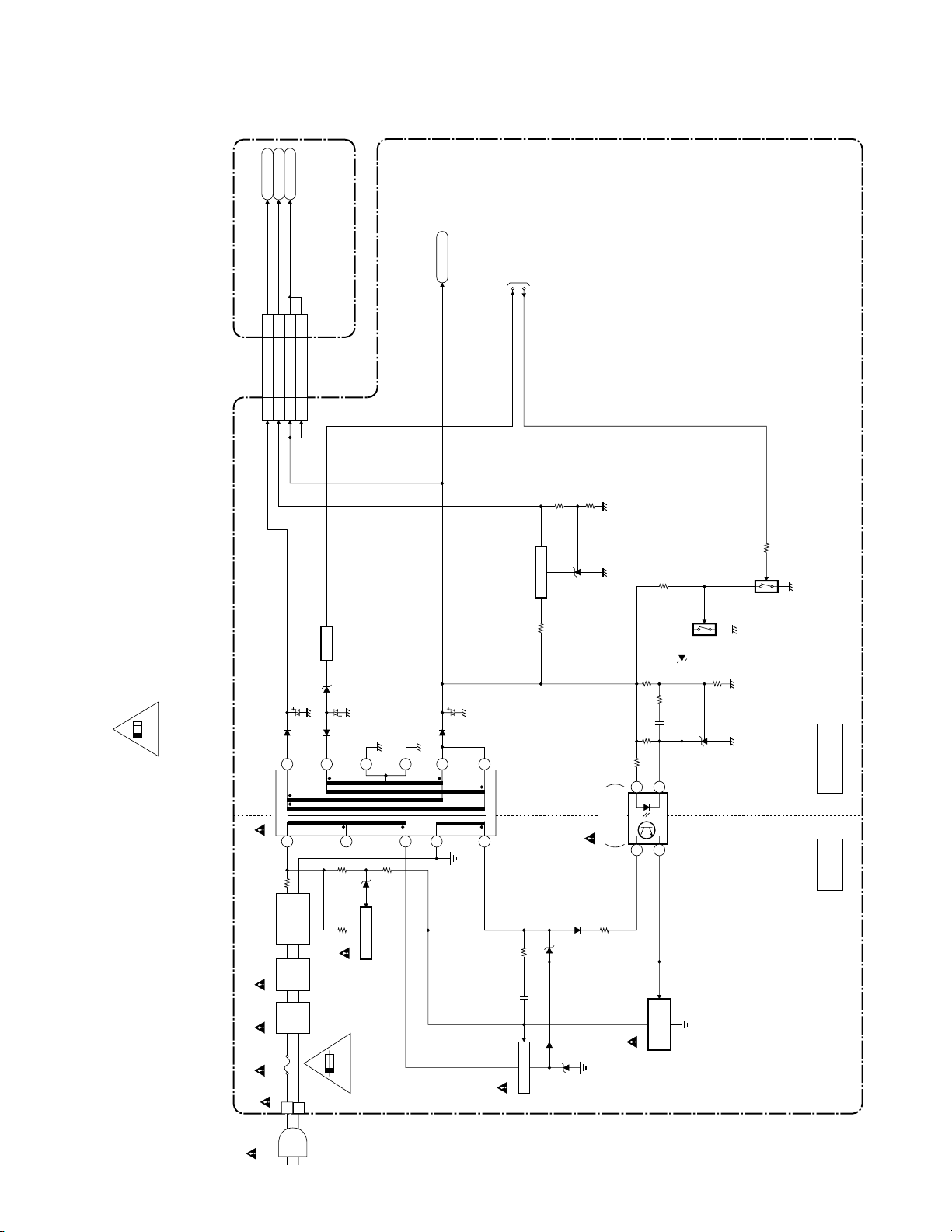
5. Power Supply Block Diagram
NOTE:
The voltage for parts in hot circuit is measured using
hot GND as a common terminal.
P-ON+21V
AL+3.3V
AMP+24V
DIGITAL MAIN CBA UNIT
11
CN3701
16,17
13,14
22,23
P-ON+21V16,17
AL+3.3V11
P-ON+21V22,23
AMP+24V13,14
CN631
P-ON+21V
TO
SYSTEM CONTROL
RESET
P-ON-H2
BLOCKDIAGRAM
POWER SUPPLY CBA
For continued protection against risk of fire,
replace only with same type 4A, 125V fuse.
RESET
Q650
CAUTION ! :
ATTENTION : Utiliser un fusible de rechange de même type de 4A, 125V.
4A 125V
8
7
T601
6
BRIDGE
RECTIFIER
D601- D604
LINE
FILTER
L602
5
Q501
9
SWITCHING
Q653
+3.3V REG.
Q656
Q652
12
11
10
1
2
4
2
1
IC601
ERROR
VOLTAGE DET
4
3
HOT COLD
CAUTION !
Fixed voltage (or Auto voltage selectable) power supply circuit is used in this unit.
If Main Fuse (F601) is blown , check to see that all components in the power supply
circuit are not defective before you connect the AC plug to the AC power supply.
Otherwise it may cause some components in the power supply circuit to fail.
LINE
FILTER
L601
F601
4A/125V
1
AC601
CN601
AC CORD
2
HOT CIRCUIT. BE CAREFUL.
4A 125V
9-5
SWITCHING
Q601
CONTROL
Q602
SWITCHING
PL12.6ABLP
Page 34

SCHEMATIC DIAGRAMS / CBA AND TEST POINTS
Standard Notes
WARNING
Many electrical and mechanical parts in this chassis
have special characteristics. These characteristics
often pass unnoticed and the protection afforded by
them cannot necessarily be obtained by using
replacement components rated for higher voltage,
wattage, etc. Replacement parts that have these
special safety characteristics are identified in this
manual and its supplements; electrical components
having such features are identified by the mark “#” in
the schematic diagram and the parts list. Before
replacing any of these components, read the parts list
in this manual carefully. The use of substitute
replacement parts that do not have the same safety
characteristics as specified in the parts list may create
shock, fire, or other hazards.
Notes:
1. Do not use the part number shown on these
drawings for ordering. The correct part number is
shown in the parts list, and may be slightly
different or amended since these drawings were
prepared.
2. All resistance values are indicated in ohms
(K = 10
3. Resistor wattages are 1/4W or 1/6W unless
otherwise specified.
4. All capacitance values are indicated in μF
(P = 10
5. All voltages are DC voltages unless otherwise
specified.
This schematic diagrams are masterized version
6.
that should cover the entire PL12.6 chassis models.
Thus some parts in detail illustrated on this
schematic diagrams may vary depend on the
model within the PL12.6 chassis.
Please refer to the parts lists for each models.
7. The Circuit Board layout illustrated on this service
manual is the latest version for this chassis at the
moment of making this service manual.
Depend on the mass production date of each
model, the actual layout of each Board may differ
slightly from this version.
3
, M = 106).
-6
μF).
10-1 PL12.6SC
Page 35
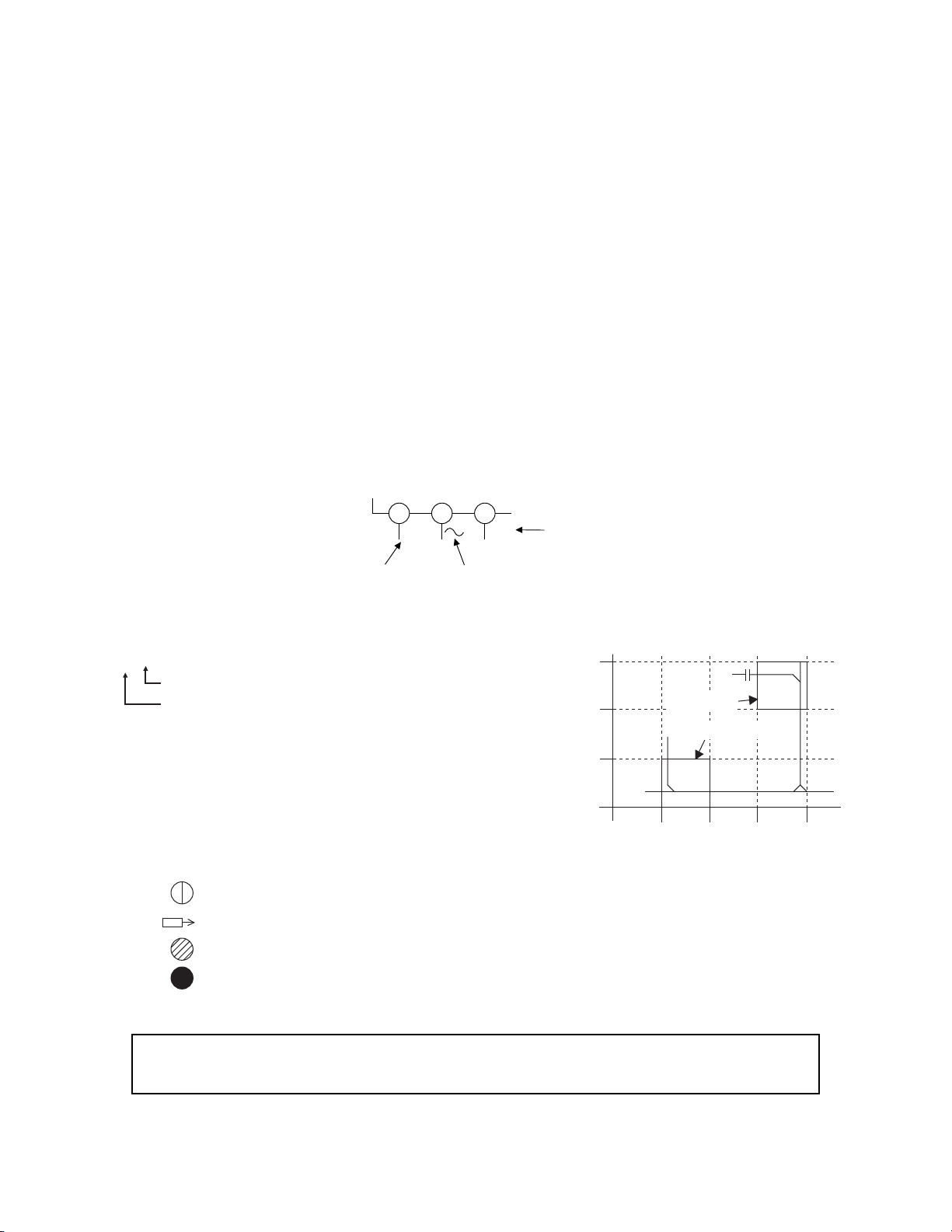
LIST OF CAUTION, NOTES, AND SYMBOLS USED IN THE SCHEMATIC DIAGRAMS ON
2
3
1
5.0 5.0
Voltage
Indicates that the voltage
is not consistent here.
Power on mode
(Unit: Volt)
1-D3
Distinction Area
Line Number
(1 to 3 digits)
Examples:
1. "1-D3" means that line number "1" goes to the line number
"1" of the area "D3".
2. "1-B1" means that line number "1" goes to the line number
"1" of the area "B1".
: Indicates a test point with a jumper wire across a hole in the PCB.
: Used to indicate a test point with a component lead on foil side.
: Used to indicate a test point with no test pin.
: Used to indicate a test point with a test pin.
THE FOLLOWING PAGES:
1. CAUTION:
CAUTION: FOR CONTINUED PROTECTION AGAINST RISK OF FIRE, REPLACE ONLY WITH SAME
TYPE_A,_V FUSE.
ATTENTION: UTILISER UN FUSIBLE DE RECHANGE DE MÊME TYPE DE_A,_V.
2. CAUTION:
Fixed Voltage (or Auto voltage selectable) power supply circuit is used in this unit.
If Main Fuse (F601) is blown, first check to see that all components in the power supply circuit are not
defective before you connect the AC plug to the AC power supply. Otherwise it may cause some components
in the power supply circuit to fail.
3. Note:
1. Do not use the part number shown on the drawings for ordering. The correct part number is shown in the
parts list, and may be slightly different or amended since the drawings were prepared.
2. To maintain original function and reliability of repaired units, use only original replacement parts which are
listed with their part numbers in the parts list section of the service manual.
4. Voltage indications on the schematics are as shown below:
Plug the TV power cord into a standard AC outlet.:
5. How to read converged lines
6. Test Point Information
The reference number of parts on Schematic Diagrams/CBA can be retrieved by
application search function.
3
AREA D3
2
1
ABCD
10-2 PL12.6SC
AREA B1
1-D3
1-B1
Page 36
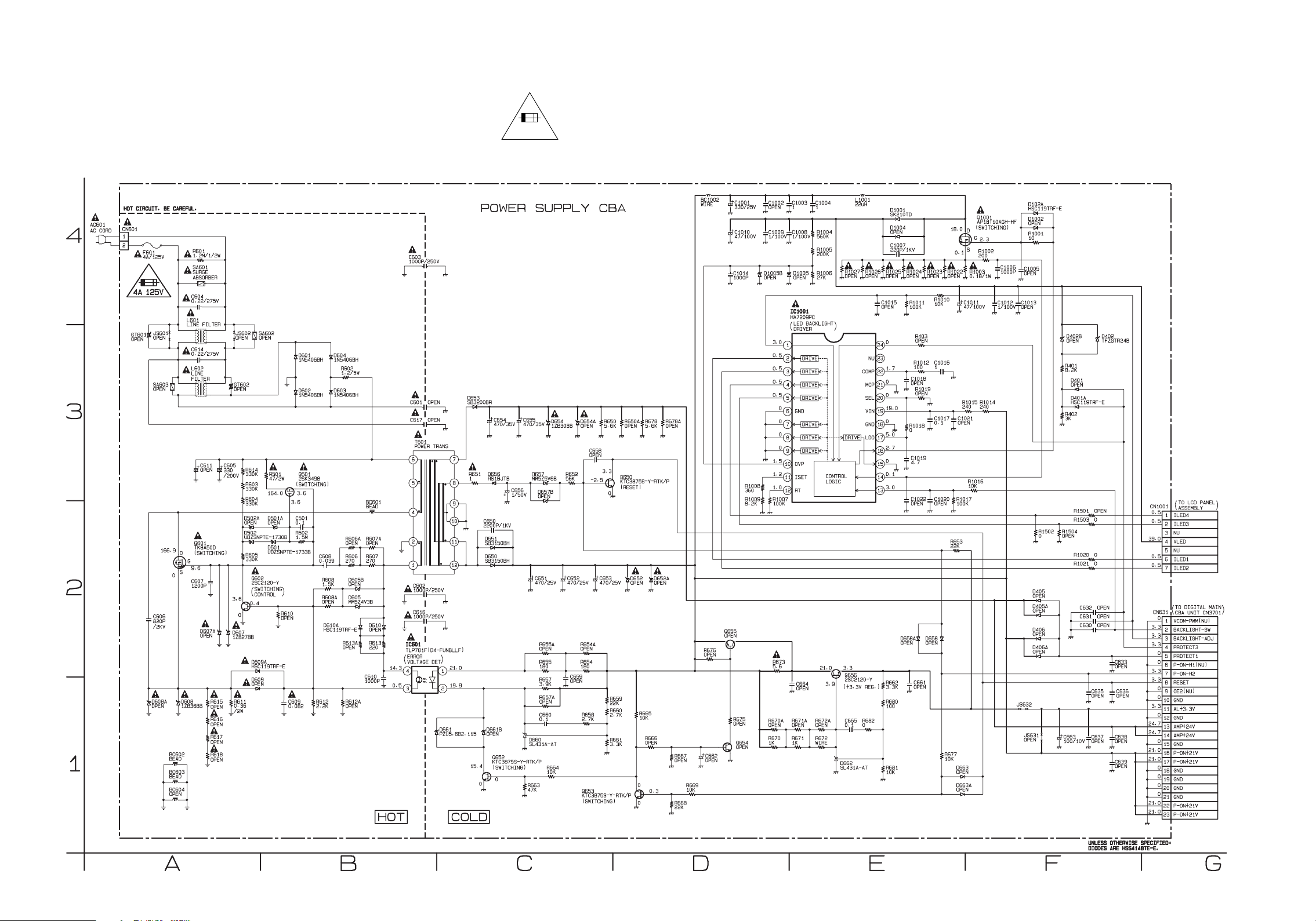
Power Supply Schematic Diagram
NOTE:
The voltage for parts in hot circuit is measured using
hot GND as a common terminal.
CAUTION !
Fixed voltage (or Auto voltage selectable) power supply circuit is used in this unit.
If Main Fuse (F601) is blown , check to see that all components in the power supply
circuit are not defective before you connect the AC plug to the AC power supply.
Otherwise it may cause some components in the power supply circuit to fail.
4A 125V
CAUTION ! :
For continued protection against risk of fire,
replace only with same type 4A, 125V fuse.
ATTENTION : Utiliser un fusible de rechange de même type de 4A, 125V.
4
3
2
1
HOT CIRCUIT. BE CAREFUL.
AC601
CN601
AC CORD
1
2
F601
4A/125V
4A 125V
GT601
OPEN
JS601
OPEN
SA603
OPEN
166.9
C606
820P
/2KV
D608A
OPEN
D
S
0
D608
1ZB36BB
BC602
BEAD
BC603
BEAD
BC604
OPEN
R601
1.2M/1/2W
SA601
SURGE
ABSORBER
C604
0.22/275V
L601
LINE FILTER
C614
0.22/275V
L602
LINE
FILTER
C605
C611
OPEN
330
/200V
Q601
TK8A50D
(SWITCHING)
G
9.6
C607
1200P
D607A
OPEN
R615
OPEN
R616
OPEN
R617
OPEN
R618
OPEN
JS602
SA602
OPEN OPEN
GT602
OPEN
R614
330K
R603
330K
R604
330K
D502A
D501A
OPEN
OPEN
D502
UDZSNPTE-1730B
D501
UDZSNPTE-1733B
R605
330K
Q602
2SC2120-Y
SWITCHING
CONTROL
3.6
0.4
0
D607
1ZB27BB
D609A
HSC119TRF-E
D609
OPEN
R611
0.36
/2W
R501
47/2W
D601
1N5406BH
D602
1N5406BH
Q501
2SK3498
(SWITCHING)
3.6164.0
3.6
C501
0.1
R502
1.5M
R610
OPEN
C609
0.082
D604
1N5406BH
R602
1.2/5W
D603
1N5406BH
C608
0.039
R608
1.5K
R608A
OPEN
D610A
HSC119TRF-E
R613A
OPEN
R612
2.2K
C603
1000P/250V
6
5
BC601
R606A
OPEN
R606
270
D605B
OPEN
D605
MM5Z4V3B
C610
1000P
R612A
OPEN
BEAD
R607A
OPEN
R607
270
D610
OPEN
R613
220
4
2
1
C602
1000P/250V
C616
1000P/250V
IC601
TLP781F(D4-FUNBLLF)
ERROR
VOLTAGE DET
14.3
4
0.5
32
HOT COLD
OPENC601
OPENC617
T601
POWER TRANS
21.0
1
19.9
D661
PZU5.6B2.115
POWER SUPPLY CBA
D653
SB3200BR
C654
C655
470/35V
D657
MM5Z5V6B
D657B
OPEN
C651
470/25V
R655A
OPEN
R655
180
R657
3.9K
R657A
OPEN
C660
0.1
D660
SL431A-AT
R663
47K
D654
1ZB30BB
R664
10K
7
8
9
10
11
12
470/35V
R651 D656
1
RS1BJTB
C650
2200P/1KV
D651
SB3150BH
D650
SB3150BH
D661B
OPEN
Q652
KTC3875S-Y-RTK/P
15.4
(SWITCHING)
0
0
C656
1/50V
R650
-2.5
C653
470/25V
5.6K
3.3
0
R659
22K
R660
2.7K
R661
3.3K
R650A
OPEN
Q650
KTC3875S-Y-RTK/P
(RESET)
D652
D654A
OPEN
C658
OPEN
R652
56K
C652
470/25V OPEN
R654A
OPEN
R654
180
C659
OPEN
R658
2.7K
Q653
KTC3875S-Y-RTK/P
(SWITCHING)
R665
10K
0
0
R678
5.6K
R666
OPEN
0.3
D652A
OPEN
R678A
OPEN
BC1002
WIRE
R676
OPEN
R667 C662
OPEN
OPEN
R669
10K
R668
22K
Q655
OPEN
C1014
1000P
R675
OPEN
C1001
330/25V
C1010
47/100V
R1008
360
R1009
8.2K
Q654
OPEN
C1002
OPEN
C1009
1/100V
D1005B
OPEN
3.0
1
0.5
2
0.5
3
0.5
4
0.5
5
0
6
0
7
0
8
0
9
1.5
10
1.2
11
1.0
12
R1007
100K
R673
5.6
R670A
OPEN
R6701KR671
1K
C10031C1004
1
C1008
R1004
1/100V
560K
R1005
200K
R1006
D1005
27K
OPEN
IC1001
HA7209PC
LED BACKLIGHT
DRIVER
DRIVE
DRIVE
DRIVE
DRIVE
GND
DRIVE
DRIVE
DRIVE
OVP
CONTROL
ISET
LOGIC
RT
21.0 3.3
3.9
C664
OPEN
R672A
R671A
OPEN
OPEN
R672
WIRE
L1001
22uH
R1027
R1026
OPEN
OPEN
24
NU
23
COMP
22
MCP
21
SEL
20
VIN
19
GND
18
17
LDO
DRIVE
16
15
14
13
Q656
2SC2120-Y
(+3.3V REG.)
R682
C665
0
0.1
D662
SL431A-AT
D1001
SK210TD
D1004
OPEN
C1007
220P/1KV
R1025
OPEN
C1015
OPEN
0
1.7
0
0
19.0
0
5.0
2.7
0
0.1
3.0
R662
3.3K
R680
100
R681
10K
R1024
OPEN
R1011
100K
C1018
OPEN
R1018
0
C1019
4.7
C1022
OPEN
D658A
OPEN
R403
OPEN
R1012
100
R1019
OPEN
C661
OPEN
R1023
OPEN
R1010
10K
C1016
1
C1017
0.1
C1020
OPEN
D658
OPEN
18.0
R1022
OPEN
R653
22K
R677
10K
0.1
R1017
100K
D663
OPEN
D663A
OPEN
Q1001
AP18T10AGH-HF
(SWITCHING)
D
G
2.3
S
R1002
200
R1003
0.18/1W
C1011
47/100V
R1015
R1014
240
240
C1021
OPEN
R1016
10K
C1006
1000P
C1012
1/100V
D102A
HSC119TRF-E
D1002
OPEN
R1001
10
C1005
OPEN
C1013
OPEN
R1502
0
D405
OPEN
D405A
OPEN
D406
OPEN
D406A
OPEN
JS632
JS631
OPEN
D402B
OPEN
R401
8.2K
D401
OPEN
D401A
HSC119TRF-E
R402
3K
R1504
OPEN
100/10V
D402
TFZGTR24B
OPENR1501
0R1503
0R1020
0R1021
OPENC632
OPENC631
OPENC630
C635
OPEN
C637C663
OPEN
C633
OPEN
C636
OPEN
C638
OPEN
C639
OPEN
TO LCD PANEL
CN1001
ASSEMBLY
0.5
1 ILED4
0.5
2 ILED3
3NU
39.0
4 VLED
5NU
0.5
6 ILED1
0.5
7 ILED2
TO DIGITAL MAIN
CBA UNIT CN3701
CN631
0
1 VCOM-PWM(NU)
3.3
2 BACKLIGHT-SW
3.3
3 BACKLIGHT-ADJ
3.3
4 PROTECT3
0
5 PROTECT1
0
6 P-ON-H1(NU)
3.3
7 P-ON-H2
3.3
8 RESET
0
9 OE2(NU)
0
10 GND
3.3
11 AL+3.3V
0
12 GND
24.7
13 AMP+24V
24.7
14 AMP+24V
0
15 GND
21.0
16 P-ON+21V
21.0
17 P-ON+21V
0
18 GND
0
19 GND
0
20 GND
0
21 GND
21.0
22 P-ON+21V
21.0
23 P-ON+21V
A FBCDE G
10-3
UNLESS OTHERWISE SPECIFIED:
DIODES ARE HSS4148TE-E.
PL12.6SCP
Page 37
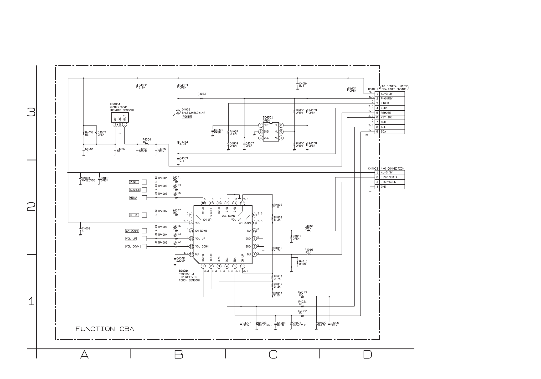
Function Schematic Diagram
3
2
1
R4051
56
C4051
10
MM5Z5V6B
C4001
1
RS4051
GP1USC32XP
(REMOTE SENSOR)
D4053
OPEN
C4003D4001
OPEN
VOUT
GND
VCC
231
C4056
10
CH DOWN
VOL UP
VOL DOWN
R4052
6.8K
C4052
1000P
POWER
SOURCE
MENU
CH UP
R4054
1K
C4055
OPEN
TP4001
TP4003
TP4005
TP4007
TP4006
TP4004
TP4002
R4063
OPEN
D4051
SMLE12WBC7W1HR
POWER
R4053
4.7K
C4053
0.1
R4001
560
R4003
560
R4005
560
R4007
560
0
19
3.3
R4006
560
R4004
560
R4002
560
20
0
21
0
22
0
23
1.0
24
C4002
2200P
IC4001
CY8C20324
-12LQXIT/CP
(TOUCH SENSOR)
R4062
0
C4058
OPEN
000003.3
MENU
SOURCE
CH UP
VDD
CH DOWN
VOL UP
VOL DOWN
NU
POWER
SOURCE
123456
3.3 3.3 3.3 3.3 3.3 3.3
R4057
OPEN
D4052
OPEN
GND
POWER
VOL DOWN
MENU
SCL
GND
VOL UP
CH DOWN
SDA
C4057
OPEN
1314151618 17
GND
GND
CH UP
IC4051
OPEN
1
OUT
2
GND
34
VCC NU
3.3
12
3.3
11
0
NU
10
0
9
0
8
0
NU
7
6
NU
5
NU
R4008
18K
R4009
8.2K
R4010
4.7K
R4011
2.7K
R4012
2.2K
R4014
2.2K
C4054
0.1
R4055
OPEN
R4058
OPEN
R4017
OPEN
R4015
OPEN
R4013
100
R4021
10
R4022
10
R4059
OPEN
R4056
OPEN
R4018
OPEN
R4016
OPEN
R4061
OPEN
TO DIGITAL MAIN
CN4001
CBA UNIT CN3101
3.3
1 AL+3.3V
5.0
2 P-ON+5V
0
3 LIGHT
3.5
4 LED1
3.3
5 REMOTE
3.3
6 KEY-IN1
0
7 GND
3.3
8 SCL
3.3
9 SDA
CN4003
(NO CONNECTION)
1 AL+3.3V
2 ISSP-SDATA
3 ISSP-SCLK
4 GND
FUNCTION CBA
C4007
OPEN
MM5Z5V6B
CBDA
10-4
C4008D4003
OPEN
D4004
MM5Z5V6B
OPEN
C4006D4002
OPEN
PL12.6SCF
Page 38
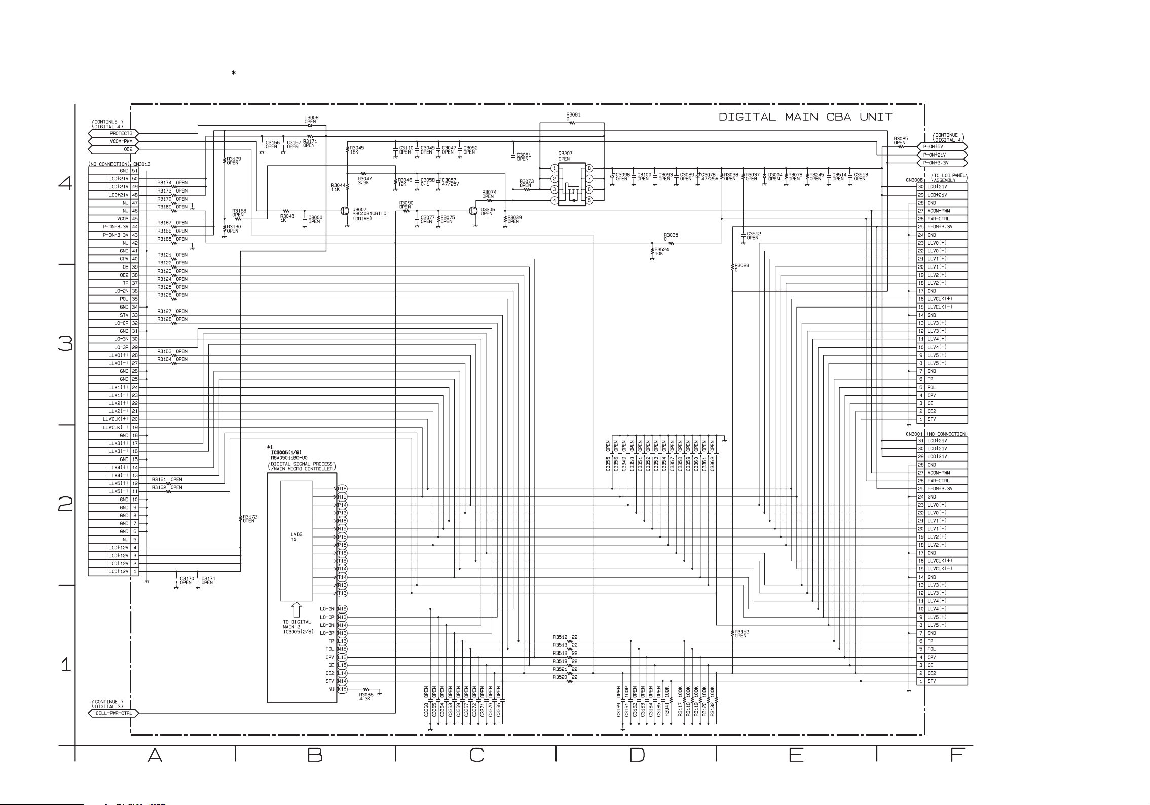
Digital Main 1 Schematic Diagram
1 NOTE:
The order of pins shown in this diagram is different from that of actual IC3005.
IC3005 is divided into six and shown as IC3005 (1/6) ~ IC3005 (6/6) in this Digital Main Schematic Diagram Section.
4
3
2
1
CONTINUE
DIGITAL 4
PROTECT3
VCOM-PWM
OE2
(NO CONNECTION)
CONTINUE
DIGITAL 3
CELL-PWR-CTRL
CN3013
51GND
50LCD+21V
49LCD+21V
48LCD+21V
47NU
46NU
45VCOM
44P-ON+3.3V
43P-ON+3.3V
42NU
41GND
40CPV
39OE
38OE2
37TP
36LO-2N
35POL
34GND
33STV
32LO-CP
31GND
30LO-3N
29LO-3P
28LLVO(+)
27LLVO(-)
26GND
25GND
24LLV1(+)
23LLV1(-)
22LLV2(+)
21LLV2(-)
20LLVCLK(+)
19LLVCLK(-)
18GND
17LLV3(+)
16LLV3(-)
15GND
14LLV4(+)
13LLV4(-)
12LLV5(+)
11LLV5(-)
10GND
9GND
8GND
7GND
6GND
5NU
4LCD+12V
3LCD+12V
2LCD+12V
1LCD+12V
OPENR3161
OPENR3162
OPENR3174
OPENR3173
OPENR3170
OPENR3169
OPENR3167
OPENR3166
OPENR3165
OPENR3121
OPENR3122
OPENR3123
OPENR3124
OPENR3125
OPENR3126
OPENR3127
OPENR3128
OPENR3163
OPENR3164
C3170
OPEN
C3171
OPEN
R3129
OPEN
R3168
OPEN
R3130
OPEN
C3166
C3167
OPEN
OPEN
R3048
1K
*1
IC3005(1/6)
R8A05011BG-U0
DIGITAL SIGNAL PROCESS
/MAIN MICRO CONTROLLER
R3172
OPEN
TO DIGITAL
MAIN 2
IC3005(2/6)
LVDS
TX
D3008
OPEN
R3171
OPEN
C3000
OPEN
R3044
11K
R16
R15
P14
P13
N16
N15
P16
P15
T16
T15
R14
T14
R13
T13
M16LO-2N
M13LO-CP
N14LO-3N
N13LO-3P
L13TP
M15POL
L16CPV
L15OE
L14OE2
M14STV
K15NU
R3045
18K
R3047
3.9K
Q3007
2SC4081UBTLQ
(DRIVE)
R3088
4.3K
C3110
OPEN
R3046
12K
R3090
OPEN
C3045
OPEN
C3058
0.1
C3077
OPEN
OPENC3368
C3047
OPEN
C3057
47/25V
R3075
OPEN
OPENC3364
OPENC3365
OPENC3363
OPENC3369
C3052
OPEN
OPENC3367
R3074
OPEN
Q3206
OPEN
OPENC3372
OPENC3371
OPENC3370
OPENC3366
C3061
OPEN
R3039
OPEN
R3073
OPEN
R3081
0
Q3207
OPEN
1
2
36
45
8
7
22R3512
22R3513
22R3518
22R3519
22R3521
22R3520
C3098
OPEN
OPENC3356
OPENC3355
OPENC3169
OPENC3349
OPENC3350
100PC3161
OPENC3162
C3100
OPEN
OPENC3352
OPENC3351
OPENC3164
OPENC3163
C3093
OPEN
R3035
0
R3524
10K
OPENC3353
OPENC3354
OPENC3165
OPENC3357
100KR3041
C3089
OPEN
OPENC3359
OPENC3358
100KR3117
100KR3118
DIGITAL MAIN CBA UNIT
C3078
47/25V
OPENC3361
OPENC3360
100KR3119
100KR3120
OPENC3362
100KR3132
R3038
OPEN
R3028
0
R3152
OPEN
R3037
OPEN
C3512
OPEN
D3004
OPEN
R3078
OPEN
R3245
OPEN
C3514
OPEN
C3513
OPEN
R3085
OPEN
P-ON+5V
P-ON+21V
P-ON+3.3V
TO LCD PANEL
ASSEMBLY
CN3006
30 LCD+21V
29 LCD+21V
28 GND
27 VCOM-PWM
26 PWR-CTRL
25 P-ON+3.3V
24 GND
23 LLV0(+)
22 LLV0(-)
21 LLV1(+)
20 LLV1(-)
19 LLV2(+)
18 LLV2(-)
17 GND
16 LLVCLK(+)
15 LLVCLK(-)
14 GND
13 LLV3(+)
12 LLV3(-)
11 LLV4(+)
10 LLV4(-)
9 LLV5(+)
8 LLV5(-)
7GND
6TP
5POL
4CPV
3OE
2OE2
1STV
CN3001
(NO CONNECTION)
31 LCD+21V
30 LCD+21V
29 LCD+21V
28 GND
27 VCOM-PWM
26 PWR-CTRL
25 P-ON+3.3V
24 GND
23 LLV0(+)
22 LLV0(-)
21 LLV1(+)
20 LLV1(-)
19 LLV2(+)
18 LLV2(-)
17 GND
16 LLVCLK(+)
15 LLVCLK(-)
14 GND
13 LLV3(+)
12 LLV3(-)
11 LLV4(+)
10 LLV4(-)
9 LLV5(+)
8 LLV5(-)
7GND
6TP
5POL
4CPV
3OE
2OE2
1STV
CONTINUE
DIGITAL 4
A
10-5
DCB
E
F
PL12.6SCAD1
Page 39
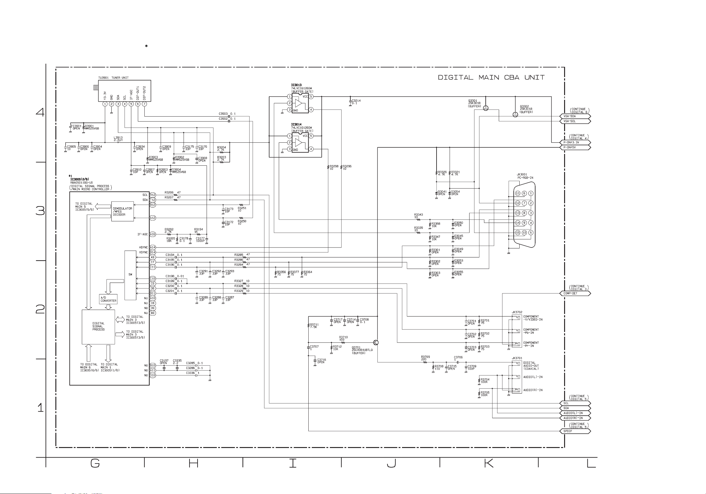
Digital Main 2 Schematic Diagram
1 NOTE:
The order of pins shown in this diagram is different from that of actual IC3005.
IC3005 is divided into six and shown as IC3005 (1/6) ~ IC3005 (6/6) in this Digital Main Schematic Diagram Section.
4
3
2
1
TU3901 TUNER UNIT
+3.3V2GND3SDA4SCL5IF-AGC6DIF-OUT17DIF-OUT2
1
C3901 D3901
OPEN
MM5Z5V6B
C3904
C3906
C3905
10
*1
IC3005(2/6)
R8A05011BG-U0
DIGITAL SIGNAL PROCESS
/MAIN MICRO CONTROLLER
OPEN
OPEN
TO DIGITAL
MAIN 5
IC3005(5/6)
DIGITAL
SIGNAL
PROCESS
TO DIGITAL
MAIN 6
IC3005(6/6)
A/D
CONVERTER
TO DIGITAL
MAIN 1
IC3005(1/6)
L3913
2.2uH
C3910
10P
DEMODULATOR
/MPEG
DECODER
SW
TO DIGITAL
MAIN 3
IC3005(3/6)
TO DIGITAL
MAIN 3
IC3005(3/6)
C3934
OPEN
MM5Z5V6B
C3907
OPEN
SCL R12
SDA T12
B12
A12
A16IF-AGC
A14HSYNC
B14VSYNC
A9
C7
C11
C10
C9
D8
B11
A10NU
C8NU
D9NU
B9NU
B10NU
A11NU
D10NU
C3909
OPEN
D3902
MM5Z5V6B
R3903 D3904
OPEN
MM5Z5V6B
47R3206
47R3207
R3202
2.7K
R3205
18K
0.1C3194
0.1C3195
0.1C3196
0.01C3198
0.1C3199
0.1C3200
0.1C3201
C3197
C3335
OPEN
C3175
33P
C3178
0.1
C3176
33P
C3908
OPEN
R3194
1K
C3177
1000P
C3291
33P
C3289
33P
0.1C32852.2
0.1C3286
1C3336
R3204
2.7K
R3203D3903
2.7K
C3292
33P
C3288
33P
0.1C3903
0.1C3902
C3173
33P
C3172
33P
C3293
33P
C3287
33P
R3251
10
R3250
10
R3285
R3286
R3284
DIGITAL MAIN CBA UNIT
IC3013
74LVC1G126GW
(BUFFER GATE)
1
VCC
5
2
34
GND
IC3014
74LVC1G126GW
(BUFFER GATE)
1
VCC
5
2
34
GND
R3298
10
47
47
47
R3364
R3377
R3356
75
10R3327
10R3328
10R3329
75
75
R3711
7.5K
C3716
OPEN
R3712
10K
C3707
1
C3717
OPEN
R3710
100
C3214
0.1
R3296
10
C3714
OPEN
Q3701
2SC4081UBTLQ
(BUFFER)
C3708
0.1
R3343
10
R3339
10
R3709
220
R3326
4.7K
D3041
OPEN
R3358
10K
R3347
10K
R3301
OPEN
R3302
OPEN
R3303
OPEN
R3708
110
C3715
OPEN
R3321
4.7K
D3054
OPEN
D3050
OPEN
D3045
OPEN
D3049
OPEN
D3053
OPEN
D3055
OPEN
C3706
1
Q3301
2SK3018
(BUFFER)
R3701
C3701
75
OPEN
R3702
C3702
75
OPEN
R3703
C3703
75
OPEN
C3709
100P
R3704
100K
R3705
100K
Q3302
2SK3018
JK3001
PC-RGB-IN
11156
12
13
14
JK3702
JK3701
DIGITAL
AUDIO-OUT
(COAXIAL)
1
2
7
3
8
4
9
5
10
COMPONENT
-Y/VIDEO-IN
COMPONENT
-Pb-IN
COMPONENT
-Pr-IN
AUDIO(L)-IN
AUDIO(R)-IN
CONTINUE
DIGITAL 6(BUFFER)
VGA-SDA
VGA-SCL
CONTINUE
DIGITAL 4
P-ON+3.3V
P-ON+5V
CONTINUE
DIGITAL 3
COMP-DET
CONTINUE
DIGITAL 5
SCL
SDA
AUDIO(L)-IN
AUDIO(R)-IN
CONTINUE
DIGITAL 5
SPDIF
GH K
JI
L
10-6
PL12.6SCAD2
Page 40
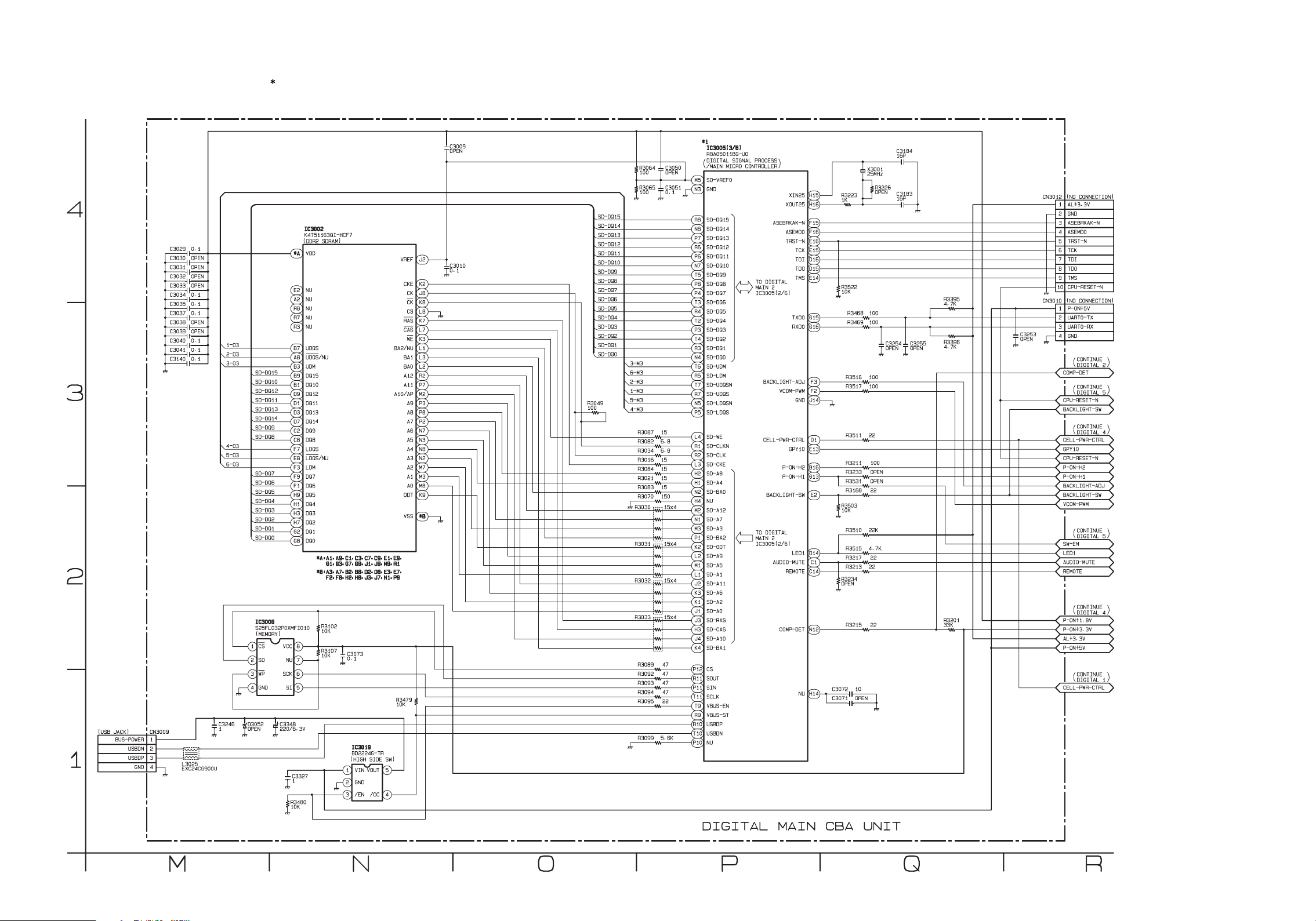
Digital Main 3 Schematic Diagram
1 NOTE:
The order of pins shown in this diagram is different from that of actual IC3005.
IC3005 is divided into six and shown as IC3005 (1/6) ~ IC3005 (6/6) in this Digital Main Schematic Diagram Section.
4
3
2
1
(USB JACK)
CN3009
1BUS-POWER
2USBDN
3USBDP
4GND
0.1C3029
OPENC3030
OPENC3031
OPENC3032
OPENC3033
0.1C3034
0.1C3035
0.1C3037
OPENC3038
OPENC3039
0.1C3040
0.1C3041
0.1C3140
C3246
1
L3025
EXC24CG900U
IC3002
K4T51163QI-HCF7
(DDR2 SDRAM)
*A VDD
E2 NU
A2 NU
R8 NU
R7 NU
R3 NU
1-O3
2-O3
3-O3
SD-DQ15
SD-DQ10
SD-DQ12
SD-DQ11
SD-DQ13
SD-DQ14
SD-DQ9
SD-DQ8
4-O3
5-O3
6-O3
SD-DQ7
SD-DQ6
SD-DQ5
SD-DQ4
SD-DQ3
SD-DQ2
SD-DQ1
SD-DQ0
IC3006
S25FL032P0XMFI010
(MEMORY)
1
CS
2
SO
3
WP
45
GND SI
D3052
OPEN
B7 UDQS
A8 UDQS/NU
B3 UDM
B9 DQ15
B1 DQ10
D9 DQ12
D1 DQ11
D3 DQ13
D7 DQ14
C2 DQ9
C8 DQ8
F7 LDQS
E8 LDQS/NU
F3 LDM
F9 DQ7
F1 DQ6
H9 DQ5
H1 DQ4
H3 DQ3
H7 DQ2
G2 DQ1
G8 DQ0
8
VCC
7
NU
6
SCK
C3348
220/6.3V
C3327
1
R3480
10K
*A:A1,A9,C1,C3,C7,C9,E1,E9,
G1,G3,G7,G9,J1,J9,M9,R1
*B:A3,A7,B2,B8,D2,D8,E3,E7,
F2,F8,H2,H8,J3,J7,N1,P9
R3102
10K
R3107
C3073
10K
0.1
IC3019
BD2224G-TR
(HIGH SIDE SW)
1
2
34
VIN
VOUT
GND
/EN /OC
5
R3479
10K
C3009
OPEN
C3050
R3064
OPEN
100
C3051
R3065
0.1
100
SD-DQ15
SD-DQ14
SD-DQ13
SD-DQ12
J2VREF
C3010
0.1
K2CKE
J8CK
K8CK
L8CS
K7RAS
L7CAS
K3WE
L1BA2/NU
L3BA1
L2BA0
R2A12
P7A11
M2A10/AP
P3A9
P8A8
P2A7
N7A6
N3A5
N8A4
N2A3
M7A2
M3A1
M8A0
K9ODT
*BVSS
SD-DQ11
SD-DQ10
SD-DQ9
SD-DQ8
SD-DQ7
SD-DQ6
SD-DQ5
SD-DQ4
SD-DQ3
SD-DQ2
SD-DQ1
SD-DQ0
R3049
100
3-M3
6-M3
2-M3
1-M3
5-M3
4-M3
15R3087
6.8R3082
6.8R3034
15R3016
15R3084
15R3021
15R3083
150R3070
R3030 15x4
R3031 15x4
R3032 15x4
R3033 15x4
5.6KR3099
47R3089
47R3092
47R3093
47R3094
22R3095
*1
IC3005(3/6)
R8A05011BG-U0
DIGITAL SIGNAL PROCESS
/MAIN MICRO CONTROLLER
M5 SD-VREF0
N3 GND
R8 SD-DQ15
N8 SD-DQ14
P7 SD-DQ13
R6 SD-DQ12
P6 SD-DQ11
N7 SD-DQ10
T5 SD-DQ9
P8 SD-DQ8
P4 SD-DQ7
T3 SD-DQ6
R4 SD-DQ5
T2 SD-DQ4
P3 SD-DQ3
T4 SD-DQ2
R3 SD-DQ1
N4 SD-DQ0
T6 SD-UDM
R5 SD-LDM
T7 SD-UDQSN
R7 SD-UDQS
N5 SD-LDQSN
P5 SD-LDQS
L4 SD-WE
R1 SD-CLKN
R2 SD-CLK
L3 SD-CKE
H2 SD-A8
H1 SD-A4
N2 SD-BA0
H4 NU
M2 SD-A12
N1 SD-A7
M3 SD-A3
P1 SD-BA2
K2 SD-ODT
L2 SD-A9
M1 SD-A5
L1 SD-A1
J2 SD-A11
K3 SD-A6
K1 SD-A2
J1 SD-A0
J3 SD-RAS
H3 SD-CAS
J4 SD-A10
K4 SD-BA1
P12 CS
R11 SOUT
P11 SIN
T11 SCLK
T9 VBUS-EN
R9 VBUS-ST
R10 USBDP
T10 USBDN
P10 NU
TO DIGITAL
MAIN 2
IC3005(2/6)
TO DIGITAL
MAIN 2
IC3005(2/6)
C3184
16P
X3001
25MHz
R3226
OPEN
H15XIN25
R3223
1K
H16XOUT25
F15ASEBRKAK-N
F16ASEMD0
E16TRST-N
E15TCK
D16TDI
D15TDO
E14TMS
R3522
10K
G15TXD0
G16RXD0
F3BACKLIGHT-ADJ
F2VCOM-PWM
J14GND
D1CELL-PWR-CTRL
E13GPY10
B16P-ON-H2
G13P-ON-H1
E2BACKLIGHT-SW
R3503
10K
D14LED1
C1AUDIO-MUTE
C14REMOTE
R3234
OPEN
N12COMP-DET
H14NU
10C3072
OPENC3071
C3183
16P
100R3468
100R3469
C3255
C3254
OPEN
OPEN
100R3516
100R3517
22R3511
100R3211
OPENR3233
OPENR3531
22R3188
22KR3510
4.7KR3515
22R3217
22R3213
22R3215 33K
R3395
4.7K
R3396
4.7K
R3201
C3253
OPEN
(NO CONNECTION)
CN3012
AL+3.3V1
2GND
3 ASEBRKAK-N
4 ASEMD0
5 TRST-N
6TCK
7TDI
8TDO
9TMS
10 CPU-RESET-N
(NO CONNECTION)
CN3010
1 P-ON+5V
2 UART0-TX
3 UART0-RX
4GND
CONTINUE
DIGITAL 2
COMP-DET
CONTINUE
DIGITAL 5
CPU-RESET-N
BACKLIGHT-SW
CONTINUE
DIGITAL 4
CELL-PWR-CTRL
GPY10
CPU-RESET-N
P-ON-H2
P-ON-H1
BACKLIGHT-ADJ
BACKLIGHT-SW
VCOM-PWM
CONTINUE
DIGITAL 5
SW-EN
LED1
AUDIO-MUTE
REMOTE
CONTINUE
DIGITAL 4
P-ON+1.8V
P-ON+3.3V
AL+3.3V
P-ON+5V
CONTINUE
DIGITAL 1
CELL-PWR-CTRL
DIGITAL MAIN CBA UNIT
MP
NO
10-7
QR
PL12.6SCAD3
Page 41
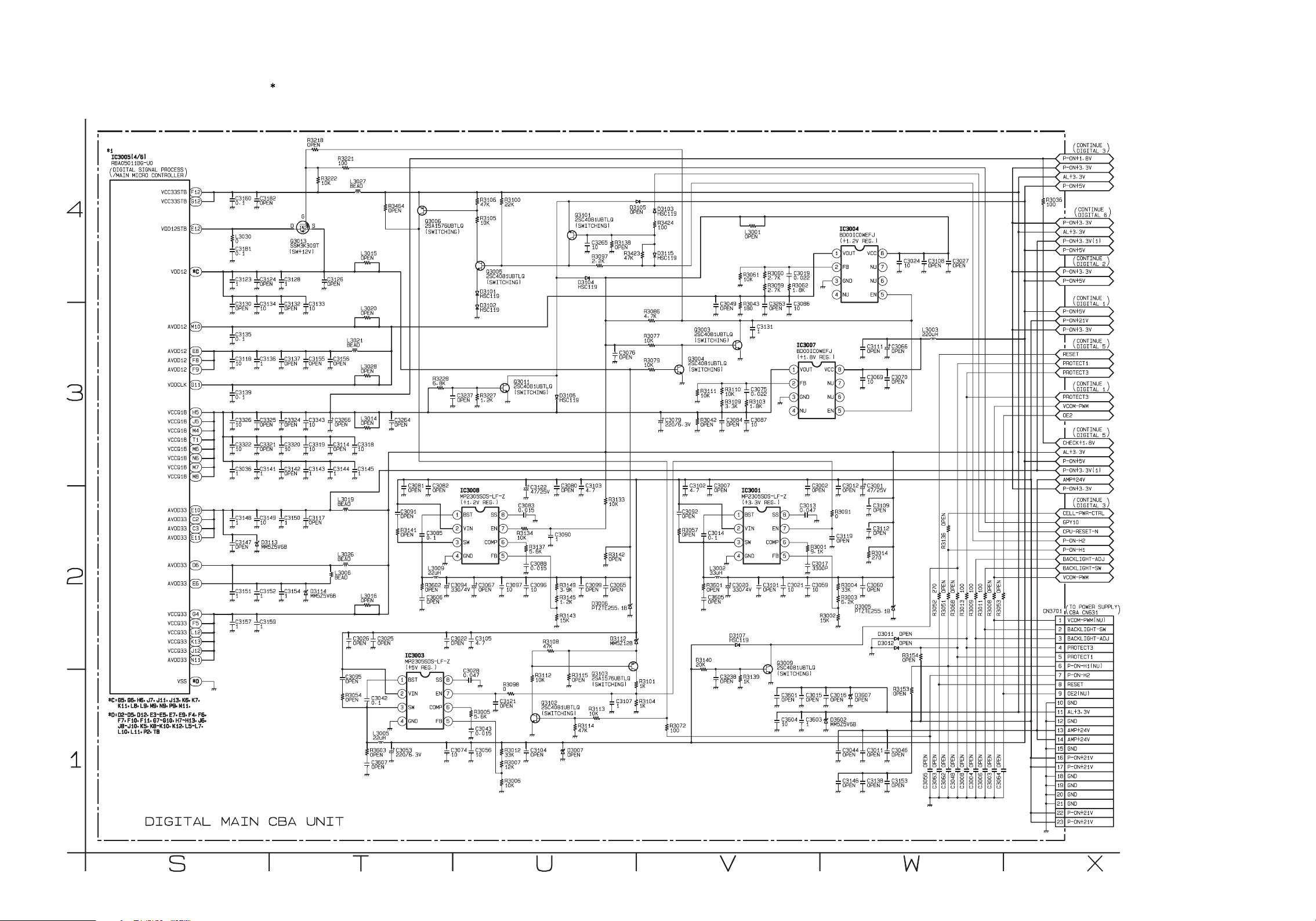
Digital Main 4 Schematic Diagram
1 NOTE:
The order of pins shown in this diagram is different from that of actual IC3005.
IC3005 is divided into six and shown as IC3005 (1/6) ~ IC3005 (6/6) in this Digital Main Schematic Diagram Section.
R3218
OPEN
R3222
10K
G
DS
Q3013
SSM3K309T
(SW+12V)
C3128
1
C313210C3133
OPEN
C3137
C3155
OPEN
OPEN
C3343
C3324
10
OPEN
C3320
C3319
10
10
C3142
C3143
OPEN
1
C3117
C3150
OPEN
1
C3154
D3114
1
MM5Z5V6B
4
3
2
*1
IC3005(4/6)
R8A05011BG-U0
DIGITAL SIGNAL PROCESS
/MAIN MICRO CONTROLLER
F12
VCC33STB
G12VCC33STB
E12VDD12STB
*CVDD12
M10AVDD12
E8AVDD12
F8AVDD12
F9AVDD12
G11VDDCLK
H5VCCQ18
J5VCCQ18
M4VCCQ18
T1VCCQ18
M6VCCQ18
N6VCCQ18
M7VCCQ18
M8VCCQ18
E10AVDD33
C2AVDD33
C3AVDD33
E11AVDD33
D6AVDD33
E6AVDD33
G4VCCQ33
F5VCCQ33
L12VCCQ33
K13VCCQ33
J12VCCQ33
N11AVDD33
*DVSS
*C:G5,G6,H6,J7,J11,J13,K6,K7,
K11,L8,L9,M9,N9,P9,M11.
*D:D2~D5,D12,E3~E5,E7,E9,F4,F6,
F7,F10,F11,G7~G10,H7~H13,J6,
J8~J10,K5,K8~K10,K12,L5~L7,
L10,L11,P2,T8
C3160
0.1
L3030
0
C3181
0.1
C3123
1
C3130
OPEN
C3135
0.1
C3118
10
C3139
0.1
C3326
10
C3322
10
C3036
1
C3148
1
C3147
OPEN
C3151
1
C3157
1
C3182
OPEN
C3124
OPEN
C3134
10
C3136
1
C3325
OPEN
C3321
OPEN
C3141
1
C3149
10
D3113
MM5Z5V6B
C3152
1
C3159
1
1
DIGITAL MAIN CBA UNIT
R3221
100
C3126
OPEN
C3156
OPEN
C3266
OPEN
C3114
OPEN
C3144
1
L3019
BEAD
L3026
BEAD
L3006
BEAD
L3027
BEAD
L3021
BEAD
C3318
10
C3145
1
C3026
OPEN
C3095
OPEN
R3054
OPEN
L3015
OPEN
L3020
OPEN
L3028
OPEN
L3014
OPEN
L3016
OPEN
C3042
0.1
R3603
OPEN
C3607
OPEN
R3464
C3025
OPEN
L3005
22uH
OPEN
Q3006
2SA1576UBTLQ
(SWITCHING)
R3228
6.8K
C3237
OPEN
C3264
OPEN
C3082
C3081
OPEN
OPEN
C3091
OPEN
R3141
OPEN
IC3003
MP2305SDS-LF-Z
(+5V REG.)
BST
1
VIN
2
SW
3
GND FB
45
C3053
220/6.3V
1
2
C3085
0.1
3
45
L3009
22uH
R3602
C3094
OPEN
330/4V 3.9K
C3606
OPEN
C3022
OPEN
SS
8
EN
7
COMP
6
C3074
10
R3106
R3100
47K
22K
R3105
10K
Q3005
2SC4081UBTLQ
(SWITCHING)
D3101
HSC119
D3102
HSC119
Q3011
2SC4081UBTLQ
(SWITCHING)
R3227
1.2K
8
7
6
C3097
10
R3098
0
C3121
OPEN
R3012
33K
R3007
12K
R3006
10K
C3083
0.015
R3134
10K
R3137
5.6K
C3122
47/25V
C3088
0.015
C3096
10
R3112
10K
C3104
OPEN
IC3008
MP2305SDS-LF-Z
(+1.2V REG.) (+3.3V REG.)
BST
SS
VIN
EN
SW
COMP
GND FB
C3067
OPEN
C3105
4.7
C3028
0.047
R3005
5.6K
C3043
0.015
C3056
10
Q3101
2SC4081UBTLQ
(SWITCHING)
D3104
HSC119
D3106
HSC119
C3080
OPEN
C3090
1
R3149
R3145
1.2K
R3143
15K
R3108
47K
R3115
OPEN
Q3102
2SC4081UBTLQ
(SWITCHING)
R3114
47K
D3007
OPEN
C3265
10
R3097
2.2K
C3103
4.7
C3099
OPEN
D3006
PTZTE255.1B
Q3103
2SA1576UBTLQ
(SWITCHING)
R3113
10K
R3138
OPEN
R3423
47K
C3076
OPEN
R3133
10K
R3142
OPEN
C3065
OPEN
D3112
MM5Z12B
C3107
1
D3105
OPEN
R3101
1K
R3104
1K
R3086
4.7K
R3077
10K
R3079
10K
D3103
HSC119
R3424
100
D3115
HSC119
C3079
220/6.3V
R3072
100
Q3003
2SC4081UBTLQ
(SWITCHING)
Q3004
2SC4081UBTLQ
(SWITCHING)
R3111
10K
R3042
OPEN
C3007
C3102
OPEN
4.7
C3092
OPEN
R3057
C3014
OPEN
0.1
L3002
33uH
R3601
OPEN
C3605
OPEN
R3140
20K
L3001
OPEN
R3060
R3061
2.7K
10K
R3059
2.7K
C3049
OPEN
R3110
10K
R3109
3.3K
C3084
OPEN
D3107
HSC119
C3238
OPEN
C3020
330/4V
C3263
R3043
OPEN
180
C3131
1
C3075
0.022
R3103
1.8K
C3087
10
IC3001
MP2305SDS-LF-Z
1
BST
2
VIN
3
SW
45
GND FB
R3139
1K
8
SS
7
EN
6
COMP
C3101
OPEN
Q3009
2SC4081UBTLQ
(SWITCHING)
C3601
OPEN
C3604
10
IC3004
BD00IC0WEFJ
(+1.2V REG.)
1
VOUT
2
C3019
0.022
R3062
1.8K
C3086
10
IC3007
BD00IC0WEFJ
(+1.8V REG.)
VOUT
1
FB
2
GND
3
NU EN
45
C3013
0.047
C3021
10
C3015
OPEN
C3603
1
FB
3
GND
45
NU EN
VCC
8
NU
7
NU
6
C3002
C3012
OPEN
OPEN
R3091
0
C3119
OPEN
R3001
9.1K
C3017
3300P
C3059
R3004
10
33K
R3003
6.2K
R3002
15K
C3016
OPEN
D3602
MM5Z5V6B
C3044
OPEN
C3146
OPEN
8
VCC
7
NU
6
NU
C3111 C3066
OPEN
OPEN
C3069
C3070
10
OPEN
C3001
47/25V
C3109
OPEN
C3112
OPEN
R3014
270
C3060
OPEN
D3005
PTZTE255.1B
D3011 OPEN
D3012 OPEN
R3153
C3011
OPEN
C3138
OPEN
OPEN
C3046
OPEN
C3153
OPEN
D3607
OPEN
C3024
10
R3154
OPEN
C3108
OPEN
L3003
220uH
OPENC3055
OPENR3136
270R3052
OPENR3051
OPENC3063
OPENC3062
C3027
OPEN
OPENR3068
100R3013
OPENC3048
OPENC3008
100R3009
100R3011
OPENC3004
OPENC3006
OPENR3008
OPENC3003
OPENC3064 OPENR3053
CONTINUE
DIGITAL 3
P-ON+1.8V
P-ON+3.3V
AL+3.3V
P-ON+5V
R3036
100
CONTINUE
DIGITAL 6
P-ON+3.3V
AL+3.3V
P-ON+3.3V(1)
P-ON+5V
CONTINUE
DIGITAL 2
P-ON+3.3V
P-ON+5V
CONTINUE
DIGITAL 1
P-ON+5V
P-ON+21V
P-ON+3.3V
CONTINUE
DIGITAL 5
RESET
PROTECT1
PROTECT3
CONTINUE
DIGITAL 1
PROTECT3
VCOM-PWM
OE2
CONTINUE
DIGITAL 5
CHECK+1.8V
AL+3.3V
P-ON+5V
P-ON+3.3V(1)
AMP+24V
P-ON+3.3V
CONTINUE
DIGITAL 3
CELL-PWR-CTRL
GPY10
CPU-RESET-N
P-ON-H2
P-ON-H1
BACKLIGHT-ADJ
BACKLIGHT-SW
VCOM-PWM
TO POWER SUPPLY
CN3701
CBA CN631
1 VCOM-PWM(NU)
2 BACKLIGHT-SW
3 BACKLIGHT-ADJ
4 PROTECT3
5 PROTECT1
6 P-ON-H1(NU)
7 P-ON-H2
8 RESET
9 OE2(NU)
10 GND
11 AL+3.3V
12 GND
13 AMP+24V
14 AMP+24V
15 GND
16 P-ON+21V
17 P-ON+21V
18 GND
19 GND
20 GND
21 GND
22 P-ON+21V
23 P-ON+21V
10-8
WSVT
XU
PL12.6SCAD4
Page 42
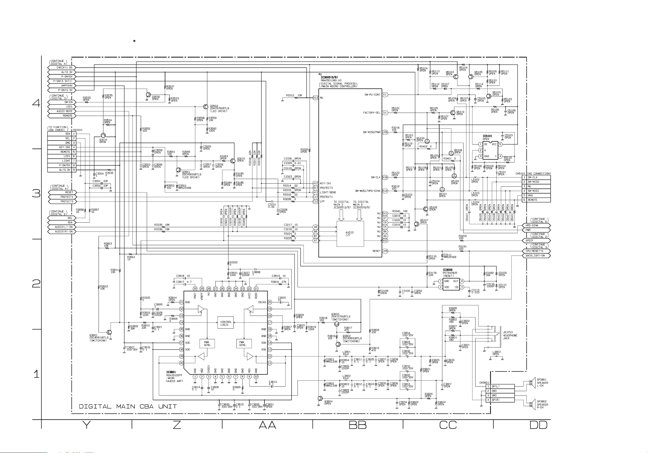
Digital Main 5 Schematic Diagram
1 NOTE:
The order of pins shown in this diagram is different from that of actual IC3005.
IC3005 is divided into six and shown as IC3005 (1/6) ~ IC3005 (6/6) in this Digital Main Schematic Diagram Section.
CONTINUE
DIGITAL 4
CHECK+1.8V
AL+3.3V
P-ON+5V
P-ON+3.3V(1)
AMP+24V
4
3
2
P-ON+3.3V
CONTINUE
DIGITAL 3
SW-EN
LED1
AUDIO-MUTE
REMOTE
TO FUNCTION
CBA CN4001
CONTINUE
DIGITAL 4
RESET
PROTECT1
PROTECT3
CONTINUE
DIGITAL 2
SCL
SDA
AUDIO(L)-IN
AUDIO(R)-IN
CN3101
1SDA
2SCL
3GND
4KEY-IN1
5REMOTE
6LED1
7LIGHT
8P-ON+5V
9AL+3.3V
R3556
10
R3532
OPEN
R3535
OPEN
R3534
OPEN
Q3531
OPEN
R3536
C3554
0
1
33PC3551
33PC3552
R3557
10
R3823
10K
R3811
10K
R3812
10K
Q3801
2SC4081UBTLQ
(SWITCHING)
R3561
10
R3806
39K
C3827
100/35V
R3552
100
C3553
OPEN
R3325
0
R3502
100K
R3813
33K
C3816
0.1
Q3530
OPEN
C3559
OPEN
C3556
OPEN
C3809
1
C3229
2200P
C3821
0.1
1
DIGITAL MAIN CBA UNIT
R3537
OPEN
R3533
OPEN
R3551
R3555
100
OPEN
Q3501
2SC4081UBTLQ
(LED DRIVE)
R3553
D3501
100
MM5Z5V6B
18KR3335
18KR3336
R3814
OPEN
31
32
33
R3808
0
34
35
36
37
38
39
40
IC3801
R2A15122FP
-W00R
(AUDIO AMP)
Q3502
2SA1576UBTLQ
(LED DRIVE)
R3558
R3559
OPEN
10K
R3560
100K
C3555
OPEN
R3183
OPEN
C3558
C3557
OPEN
OPEN
10C3818
4.7C3817
NU
VREFF
PWM
GENE.
HB2
DVDD1
C3828
10
GND
GND
PROT
GND
GND
GND
VDD
VDD
GND
12345678910
C3814
0.1
R3184
OPEN
OPENC3221
OPENC3222
R3322
0
R3501
100K
GND
CONTROL
LOGIC
GND GND
GND
C3829
100/35V
R3185
OPEN
R3186
OPEN
1000PC3233
OPENR3500
GND
GND
R3826
0
C3815
0.1
Q3010
OPEN
1000PC3232
C3227
2200P
PWM
GENE.
OPENR3499
GND
GND
22KR3318
10KR3317
C3808
1
21222324252627282930
ROSC
AVCC
CBIAS
HB1
GND
C3826
100/35V
10KR3319
GND
GND
VDD
VDD
C3831
OPEN
C3231
0.22
20
19
18
17
16
15
14
13
12
11
C3813
0.1
C3328
OPEN
10C3819
27KR3810
C3820
10
R3807
OPEN
10KR3312
OPENC3330
0.01C3329
OPEND3116
OPENC3323
22R3314
OPENR3315
22R3316
0R3208
10C3217
10C3218
0R3224
0R3225
R3809
OPEN
C3833
OPEN
R3320
OPEN
R3819
100K
*1
IC3005(5/6)
R8A05011BG-U0
DIGITAL SIGNAL PROCESS
/MAIN MICRO CONTROLLER
D13 NU
A15 KEY-IN1
B13 PROTECT3
A13 LIGHT-SENS
C13 PROTECT1
C12 LPF
A8
B8
B7
A7
R3818
10K
Q3804
OPEN
R3816
10K
D3801
MM5Z33B
D3802
MM5Z33B
TO DIGITAL
MAIN 2
IC3005(2/6)
AUDIO
I/F
Q3803
2SA1576UBTLQ
(SWITCHING)
R3817
47K
Q3802
2SC4081UBTLQ
(SWITCHING)
L3801
33uH
R3804
10
C3806
1000P
L3802
33uH
R3803
10
C3805
1000P
TO DIGITAL
MAIN 6
IC3005(6/6)
R3805
10K
R3815
47K
C3811
C3825
0.1
0.1
C3824
C3812
0.1
0.1
E1SW-PU-CONT
G1FACTORY-SEL
J16SM-MISO/PWR
K16SM-CLK
K14SM-MOSI/HPD-SINK
D11NU
D7NU
C6NU
C5NU
B6NU
A6NU
N10
J15RESET
D3108
OPEN
C3837
OPEN
C3835
OPEN
R5121
OPEN
R3216
100
R5122
OPEN
R3210
100
C3838
OPEN
C3836
OPEN
R5103
OPEN
R5119
OPEN
C5102
OPEN
10KR3340
10C3219
10C3220
10C3216
C3106
1
C3804
100/35V
C3823
100/35V
C3832
100/35V
C3810
100/35V
C3822
100/35V
C3803
100/35V
C3834
OPEN
R5117
OPEN
R3822
OPEN
R5124
OPEN
Q5109
OPEN
R5118
OPEN
Q5107
OPEN
C3252
OPEN
R5116
OPEN
R3178
220
R3821
OPEN
R3820
OPEN
R5104
Q5104
OPEN
R5109
OPEN
Q5110
OPEN
Q5108
OPEN
0R3401
R5105
OPEN
Q5102
OPEN
D3111
MM5Z5V6B
IC3009
PST8429UR
(RESET)
GND OUT
CDVDD
R3828
OPEN
R3802
180
R3827
OPEN
R3801
180
C3830
OPEN
C3807
OPEN
OPEN
R5107
OPEN
R3209
100
R3191
100
32
C3802
OPEN
C3801
OPEN
OPENC5101
R5113
OPEN
D5107
R5112
OPEN
OPEN
R5125
OPEN
R5127
OPEN
0R3402
R5120
OPEN
R5101
OPEN
C5104
OPEN
Q5101
OPEN
Q5106
OPEN
14
R3825
OPEN
R3824
OPEN
Q5105
OPEN
R5114
OPEN
R5108
OPEN
L5102
OPEN
L5103
OPEN
L5104
OPEN
C3113
0.033
C5105
OPEN
IC5101
OPEN
1OE
2A
3 GND 4Y
D5106
OPEN
OPEND5105
OPENC5109
R3182
56K
C3116
1000P
CN3801
1 SP(L)
2 GND
3 GND
4 SP(R)
R5106
OPEN
R5110
OPEN
Q5103
OPEN
R5126
OPEN
OPENC5108
OPEND5104
L3803
OPEN
R5111
OPEN
R5123
OPEN
C5103
OPEN
5VCC
R5115
OPEN
R5102
OPEN
L5101
OPEN
OPEND5102
OPEND5103
D3109
OPEN
D3110
OPEN
JK3703
HEADPHONE
JACK
C5106
OPEN
OPEND5101
OPENC5107
(NO CONNECTION)
CN5101
1 SM-CLK
2 SM-MISO
3NU
4 SM-MISI
5 GND
6 REMOTE
HPD-SINK
PWR
SPDIF
CPU-RESET-N
BACKLIGHT-SW
CONTINUE
DIGITAL 6
CONTINUE
DIGITAL 2
CONTINUE
DIGITAL 3
SP3801
SPEAKER
L-CH
SP3802
SPEAKER
R-CH
YCCBBAAZDD
10-9
PL12.6SCAD5
Page 43
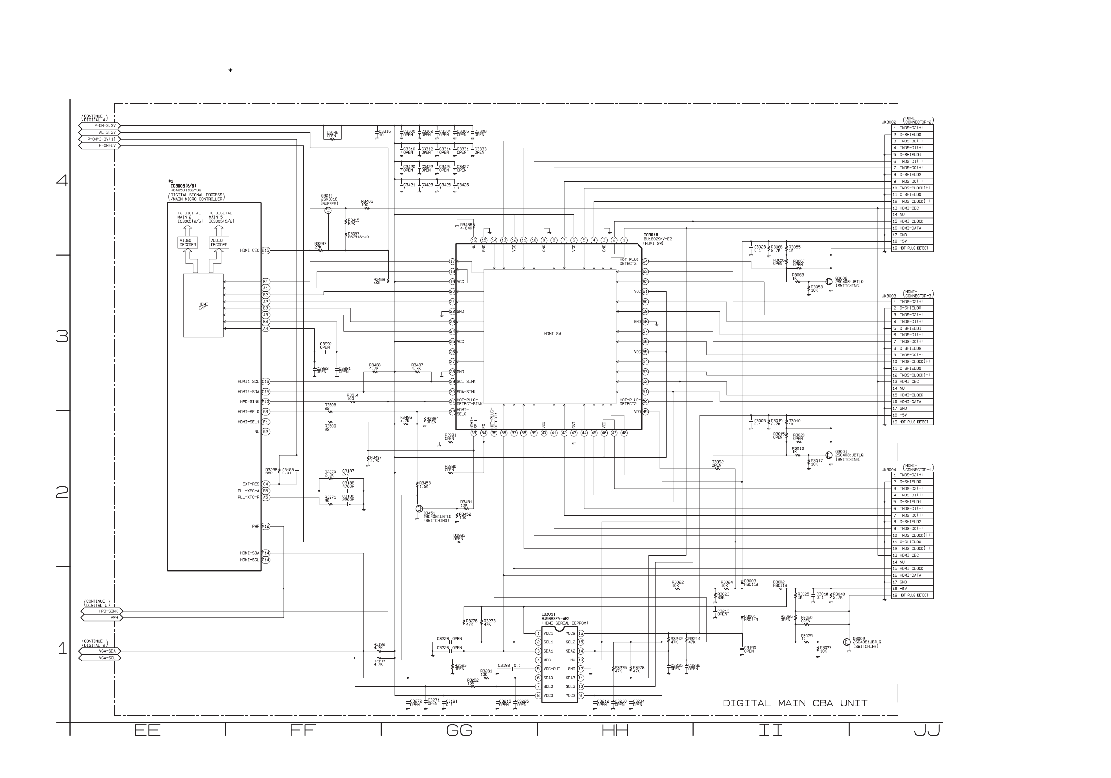
Digital Main 6 Schematic Diagram
1 NOTE:
The order of pins shown in this diagram is different from that of actual IC3005.
IC3005 is divided into six and shown as IC3005 (1/6) ~ IC3005 (6/6) in this Digital Main Schematic Diagram Section.
4
3
2
1
CONTINUE
DIGITAL 4
P-ON+3.3V
AL+3.3V
P-ON+3.3V(1)
P-ON+5V
CONTINUE
DIGITAL 5
HPD-SINK
CONTINUE
DIGITAL 2
VGA-SDA
VGA-SCL
PWR
*1
IC3005(6/6)
R8A05011BG-U0
DIGITAL SIGNAL PROCESS
/MAIN MICRO CONTROLLER
VIDEO
DECODER
TO DIGITAL
MAIN 5
IC3005(5/6)
AUDIO
DECODER
HDMI
I/F
TO DIGITAL
MAIN 2
IC3005(2/6)
HDMI-CEC B15
B1
A1
B2
A2
B3
A3
B4
A4
C16HDMI1-SCL
C15HDMI1-SDA
F13HPD-SINK
G3HDMI-SEL0
F1HDMI-SEL1
G2NU
C4EXT-RES
B5PLL-XFC-A
A5PLL-XFC-P
M12PWR
F14HDMI-SDA
G14HDMI-SCL
R3236
560
C3185
0.01
L3046
OPEN
Q3014
2SK3018
(BUFFER)
R3237
27K
C3990
OPEN
C3992
OPEN
R3508
22
R3509
22
R3270
2.2K
R3271
3K
R3415
82K
D3057
RB751S-40
C3991
OPEN
R3514
100
C3187
2.2
C3186
4700P
C3188
2200P
R3405
100
R3488
4.7K
R3489
10K
R3497
4.7K
R3192
4.7K
R3193
4.7K
C3316
10
C3300
OPEN
C3310
OPEN
C3420
OPEN
C3421
1
R3496
4.7K
C3302
OPEN
C3312
OPEN
C3422
OPEN
C3423
1
R3487
4.7K
R3994
OPEN
R3453
1.5K
Q3451
2SC4081UBTLQ
(SWITCHING)
C3272
OPEN
C3271
OPEN
C3304
OPEN
C3314
OPEN
C3424
OPEN
C3425
1
17
18
19 VCC
20
21
22 GND
23
24
25 VCC
26
27
28 GND
29 SCL-SINK
30 SDA-SINK
31
32
R3991
OPEN
R3990
OPEN
C3191
0.1
C3306
OPEN
C3331
OPEN
C3427
OPEN
C3426
1
R3486
4.64K
16
HOT-PLUGDETECT-SINK
HDMISEL0
HDMI-
33
R3451
10K
R3452
10K
D3993
OPEN
R3276
47K
OPENC3228
OPENC3226
R3523
OPEN
R3282
100
C3308
OPEN
C3333
OPEN
NU
SEL1
34EQ35
R3281
100
GND
HOT-PLUG-
R3273
47K
131415
DETECT1
36 37 38
C3215
OPEN
VCC2
SCL2
SDA2
NU
GND
SDA3
SCL3
VCC
GND
4
56
45 46
44
16
15
14
13
12
11
10
789
GND
HDMI SW
VCC
41 42 43
IC3011
BU9883FV-WE2
(HDMI SERIAL EEPROM)
VCC1
1
2
SCL1
3
SDA1
WPB
4
VCC-OUT
5
SDA0
6
SCL0
7
VCC0 VCC3
89
VCC
0.1C3192
C3225
OPEN
10
1112
39 40
GND
VCC
C3212
OPEN
123
HOT-PLUGDETECT3
HOT-PLUGDETECT2
47 48
R3275
47K
C3230
OPEN
IC3018
BU16029KV-E2
(HDMI SW)
64
63
62
61VCC
60
59
58GND
57
56
55VCC
54
53
52
51
50
49VDD
R3278
47K
C3234
OPEN
R3022
10K
R3212
47K
C3235
OPEN
R3214
47K
C3236
OPEN
R3066
2.7K
R3056
OPEN
R3019
2.7K
R3015
OPEN
D3002
HSC119
R3055
1K0.1
R3010
1K
R3026
OPEN
R3067
OPEN
R3063
1K
R3020
OPEN
R3018
1K
R3025
1K
R3050
OPEN
R3029
1K
R3058
10K
R3017
10K
C3018
R3027
10K
R3040
2.7K0.1
R3992
OPEN
R3023
33K
C3213
OPEN
R3024
10K
C3023
C3005
0.1
D3003
HSC119
D3001
HSC119
C3190
OPEN
DIGITAL MAIN CBA UNIT
Q3008
2SC4081UBTLQ
(SWITCHING)
Q3001
2SC4081UBTLQ
(SWITCHING)
Q3002
2SC4081UBTLQ
(SWITCHING)
HDMI-
JK3002
CONNECTOR-2
1 TMDS-D2(+)
2 D-SHIELD0
3 TMDS-D2(-)
4 TMDS-D1(+)
5 D-SHIELD1
6 TMDS-D1(-)
7 TMDS-D0(+)
8 D-SHIELD2
9 TMDS-D0(-)
10 TMDS-CLOCK(+)
11 C-SHIELD0
12 TMDS-CLOCK(-)
13 HDMI-CEC
14 NU
15 HDMI-CLOCK
16 HDMI-DATA
17 GND
18 +5V
19 HOT PLUG DETECT
HDMICONNECTOR-3
JK3003
1 TMDS-D2(+)
2 D-SHIELD0
3 TMDS-D2(-)
4 TMDS-D1(+)
5 D-SHIELD1
6 TMDS-D1(-)
7 TMDS-D0(+)
8 D-SHIELD2
9 TMDS-D0(-)
10 TMDS-CLOCK(+)
11 C-SHIELD0
12 TMDS-CLOCK(-)
13 HDMI-CEC
14 NU
15 HDMI-CLOCK
16 HDMI-DATA
17 GND
18 +5V
19 HOT PLUG DETECT
HDMI-
JK3004
CONNECTOR-1
1 TMDS-D2(+)
2 D-SHIELD0
3 TMDS-D2(-)
4 TMDS-D1(+)
5 D-SHIELD1
6 TMDS-D1(-)
7 TMDS-D0(+)
8 D-SHIELD2
9 TMDS-D0(-)
10 TMDS-CLOCK(+)
11 C-SHIELD0
12 TMDS-CLOCK(-)
13 HDMI-CEC
14 NU
15 HDMI-CLOCK
16 HDMI-DATA
17 GND
18 +5V
19 HOT PLUG DETECT
EE FF GG HH II JJ
10-10
PL12.6SCAD6
Page 44
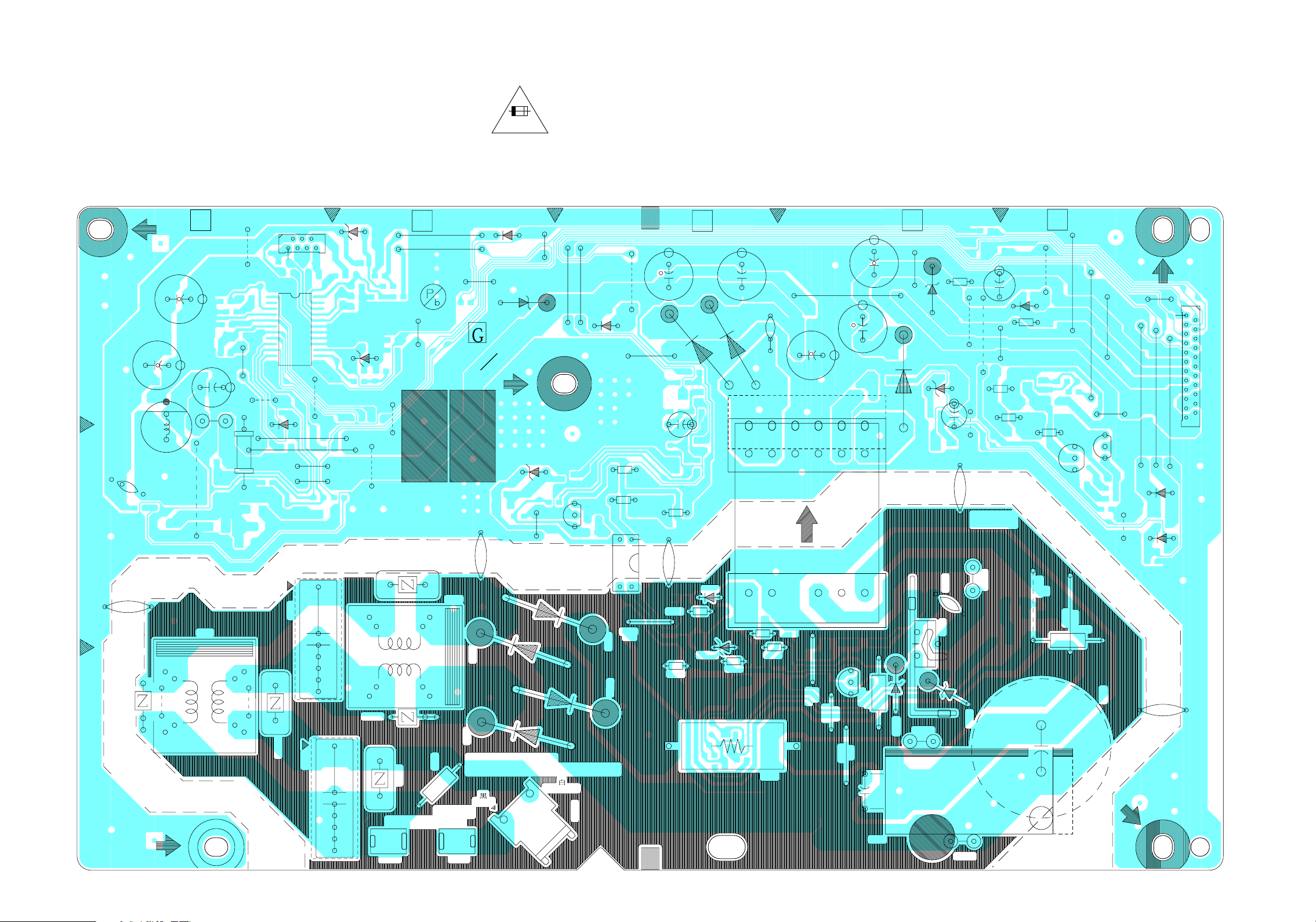
Power Supply CBA Top View
NOTE:
The voltage for parts in hot circuit is measured using
hot GND as a common terminal.
CAUTION !
Fixed voltage (or Auto voltage selectable) power supply circuit is used in this unit.
If Main Fuse (F601) is blown , check to see that all components in the power supply
circuit are not defective before you connect the AC plug to the AC power supply.
Otherwise it may cause some components in the power supply circuit to fail.
6
7
GND
J134
D1005B
D402B
J129
J128
P-ON+21V
P-ON+21V
GND
GND
GND
J124
BC
PROTECT3
GND
J123
C7A3 A3
J125
GND
C1010
C1007
C1011
L1001
A
GND
BC1002
J135
1.ILED4
2.ILED3
3.NC
4.VLED
5.NC
6.ILED1
7.ILED2
J131
C1001
R1003
VCC
J130
GND
J133
GND
CN1001
2
1
D1002
J127
J126
BA21F0F0102 5
SA603
C617
C614
L601
GT601
JS601
JS602
GT602
SA602
C604
SA601
4A/125V
FH602
CAUTION ! :
4A 125V
J122
GND
C601
D602
D601
LIVE
D401
J120
J121
BL-ADJ
L602
RISK OF FIRE-
R601
REPLACE FUSE AS MARKED
F601
FH601
ATTENTION : Utiliser un fusible de rechange de même type de 4A, 125V.
J119
PROTECT3
D652
D661B
J118
GND
J114
NEUTRAL
P-ON-H2+
CN601
For continued protection against risk of fire,
replace only with same type 4A, 125V fuse.
C653
D651
D610
R608
J117
ALL+5-CONT.
D406
J115
GND
R655
D660
IC601
D603
D604
J116
R657
J605
C651
PROTECT1
D650
C662
R654
C603
R613
GND
D605B
R612
R606
R602
C650
R607
C650
J113
P-ON+21V
GND
J606
J607
C652
GND
C655
J608
GND
C654
Q602
R611
C605
T601
Because a hot chassis ground is present in the power supply
circuit, an isolation transformer must be used when repairing.
Also, in order to have the ability to increase the input slowly,
when troubleshooting this type of power supply circuit,
a variable isolation transformer is required.
D405
R678
J110
R672
+B
JS501
E
J109
PROTECT1
Q656
J609
GND
GND
R501
J108
J106
GND
ALL+5V-CONT.
J107
P-ON+21V
D662
J101
C611
D608
D
GND
J111
D657B
BC603
D654
D653
R650
P-ON+21V
C656
C606
Q601
JS631
for Z-SoC
BC602
J132
ALL+3.3V forR-SoC
ALL+5.3V forP-SoC
JS632
R670
R671
GND
J112
COLD
C602
HOT
BC601
D607
C663
GND
GND
D658
J104
J105
GND
J103
RESET
D663
C616
1
P-ON-H2+
23
1.GND
J102
2.BL-SW
P-ON-H2
3.BL-ADJ
4.P3
5.P1
6.GND
7.P-ON-H2
8.RESET
9.GND
10.GND
11.ALL+3.3V
/ALL+5.3V
12.GND
13.AMP+24V
14.AMP+24V
15.GND
16.17.21V
18.19.20.21.GND
22.23.21V
CN631
2
10-11
BA21F0F01025
Page 45
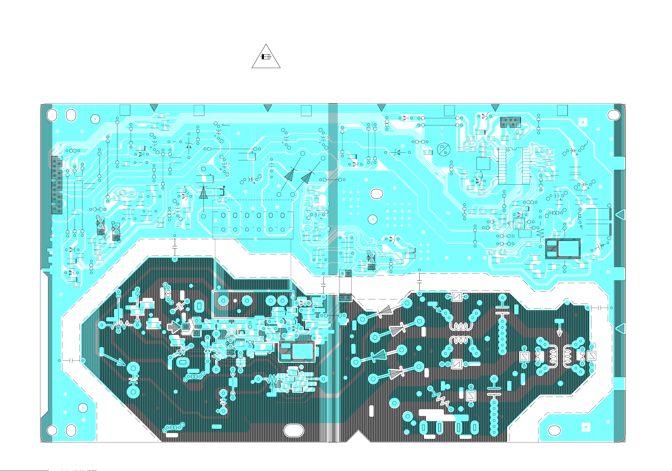
Power Supply CBA Bottom View
NOTE:
The voltage for parts in hot circuit is measured using
hot GND as a common terminal.
CAUTION !
Fixed voltage (or Auto voltage selectable) power supply circuit is used in this unit.
If Main Fuse (F601) is blown , check to see that all components in the power supply
circuit are not defective before you connect the AC plug to the AC power supply.
Otherwise it may cause some components in the power supply circuit to fail.
CN631
1
2
1.GND
2.BL-SW
3.BL-ADJ
4.P3
5.P1
6.GND
7.P-ON-H2
8.RESET
9.GND
10.GND
11.ALL+3.3V
/ALL+5.3V
12.GND
13.AMP+24V
14.AMP+24V
15.GND
16.17.21V
18.19.20.21.GND
22.23.21V
J105
GND
P-ON-H2+
23
P-ON-H2
J102
D663
C636
C616
C639
C635
J103
RESET
D663A
R677
D658
D658A
C637
R678A
J104
R682
GND
GND
J107
P-ON+21V
D662
R681
J101
GND
J106
ALL+5V-CONT.
J108
R672A
C665
R662
R680
C661
R501
C611
C664
GND
J109
R676
J609
E
PROTECT1
C638
R675
R672
Q656
R614
Q655
+B
J110
D405A
R678
JS501
D405
R673
R670A
R671A
R603
C633
C663
ALL+5.3V forP-SoC
J132
GND
R670
R671
R653
C658
BC601
R604
C632
C631
C630
R650
ALL+3.3V forR-SoC
R650A
for Z-SoC
JS631
JS632
D657
J112
GND
C602
R605
D607
P-ON+21V
D654A
D657B
C656
Q650
C606
Q601
BC603
D654
R652
D653
D
GND
J111
T601
R615
D608
D656
R651
R616
C607
Q602
R611
C654
C655
P-ON+21V
C652
R617
D609A
J608
GND
R610
GND
J113
D652A
J607
C608
GND
4A 125V
C609
R618
J606
D607A
CAUTION ! :
For continued protection against risk of fire,
replace only with same type 4A, 125V fuse.
ATTENTION : Utiliser un fusible de rechange de même type de 4A, 125V.
D661B
J114
GND
D401
D652
R661
C650
R606
R606A
R602
C650
R607A
D502A
R607
D502
D610A
D605
R608
C653
D501
D651
R666
Q653
R665
Q654
C662
R659
R654
D610
D605B
C659
R502
C501
D501A
R669
C651
R668
R663
R654A
C603
C610
R613
R613A
R612
Q501
D650
R667
R664
R608A
R612A
PROTECT1
J116
J115
GND
R657
R657A
R655A
J605
GND
D406A
D406
D604
R655
C660
IC601
D603
R658
PROTECT3
ALL+5-CONT.
J117
P-ON-H2+
J118
Q652
R660
D660
J119
Because a hot chassis ground is present in the power supply
circuit, an isolation transformer must be used when repairing.
Also, in order to have the ability to increase the input slowly,
when troubleshooting this type of power supply circuit,
a variable isolation transformer is required.
R1006
R1007
GND
SA601
R1011
J125
R403
J124
GND
GT602
D402B
D402
C1015
R1502
R1504
D1005
D1005B
R1008
R1018
J129
GND
J128
GND
P-ON+21V
P-ON+21V
R1005
R1020
C1014
C1019
C1020
R1016
R1025
J120
J121
BL-ADJ
J122
GND
D401A
BA21F0F0102 5
D661
D661A
C601
L602
D602
D601
BC
PROTECT3
J123
GND
R601
R402
R401
R1010
R1009
SA603
CN1001
6
7
12
J134
GND
R1017
J127
J126
R1021
IC1001
C1022
D1002
C1006
C604
R1026
C614
2
1
R1503
R1001
R1014
R1002
R1024
SA602
R1501
24
GND
J133
J130
GND
R1012
C1021
13
D102A
R1027
VCC
JS602
1.ILED4
2.ILED3
3.NC
4.VLED
5.NC
6.ILED1
7.ILED2
C1018
J131
C1001
BC1002
R1003
C1005
R1023
C1016
R1019
C1017
R1015
C1004
L601
A
J135
C1002C1003
GND
Q1001
C1011
L1001
R1022
JS601
C1013
C1008
C1010
C1012
C1009
D1004
D1001
C1007
R1004
C617
GT601
BC602
C605
10-12
CN601
F601
4A/125V
FH601
FH602
BA21F0F01025
Page 46
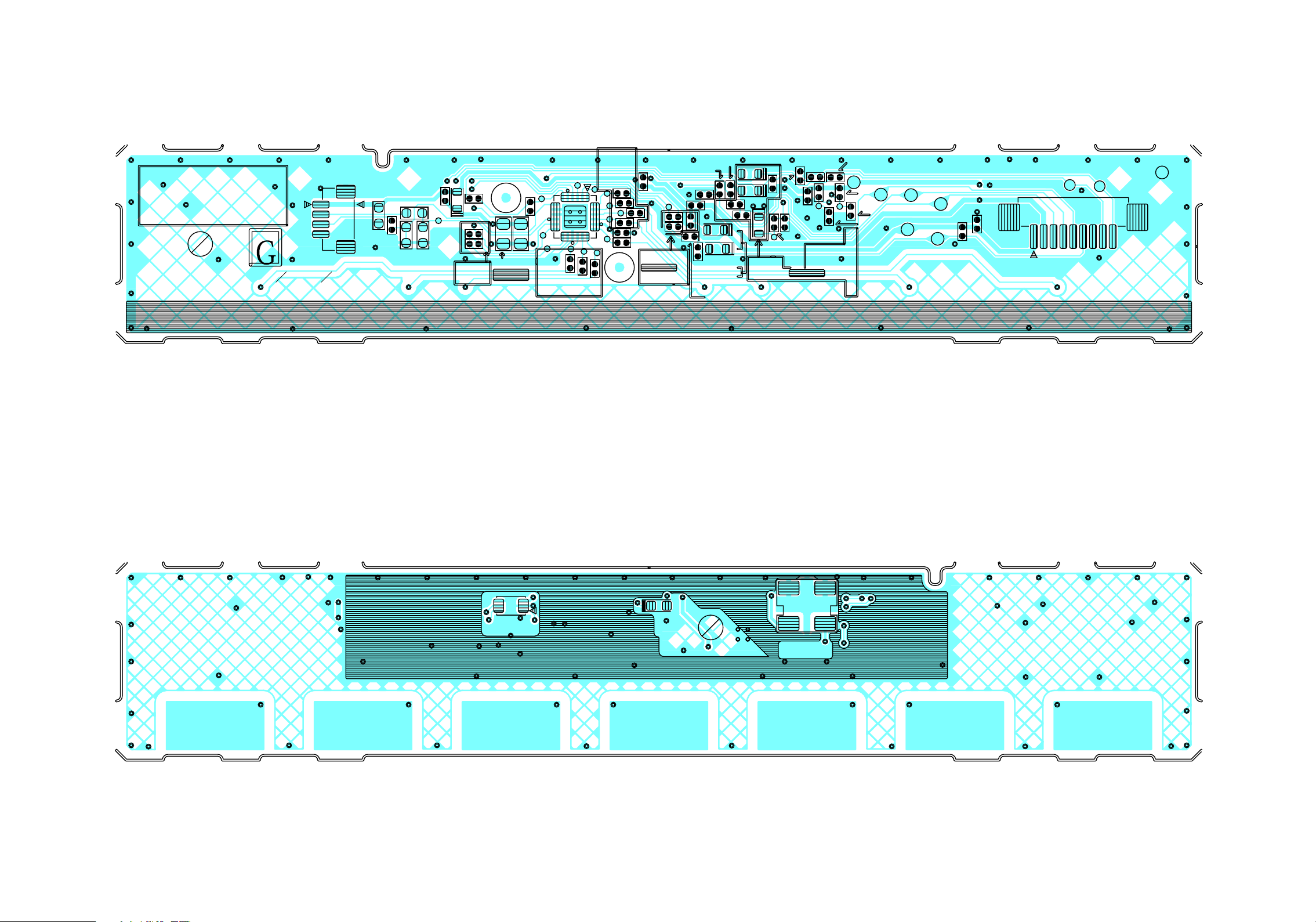
Function CBA Top View
P
b
NO.1
A30C5 C7A3
POWER
Function CBA Bottom View
CN4003
SOURCE
A3
C4003
R4018
R4016
R4015
R4051
R4017
D4053
R4011
4R4009
R4008
C4056
R4010
C4051
R4001
IC4001
R4003
R4005
C4002
R4002
R4004
R4006
R4052
R4062
C4001
R4007
R4012
R4014
R4053
C4053
R4063
C4006
C4052
D4001
D4002
R4013
R4054
C4055
CHDOWNCHUPMENU
C4008
C4057 C4058
R4057
R4022
R4059
D4004
D4003
R4021
TP4057
R4055
TP4058
TP4055
R4058
R4056
C4007
D4052
TP4059
TP4056
TP4060
BA21F0G0203 2
R4061
C4054
TP4061
CN4001
TP4062
TP4054
VOLDOWNVOLUP
IC4051
D4051
10-13
P
b
RS4051
BA21F0G02032
Page 47
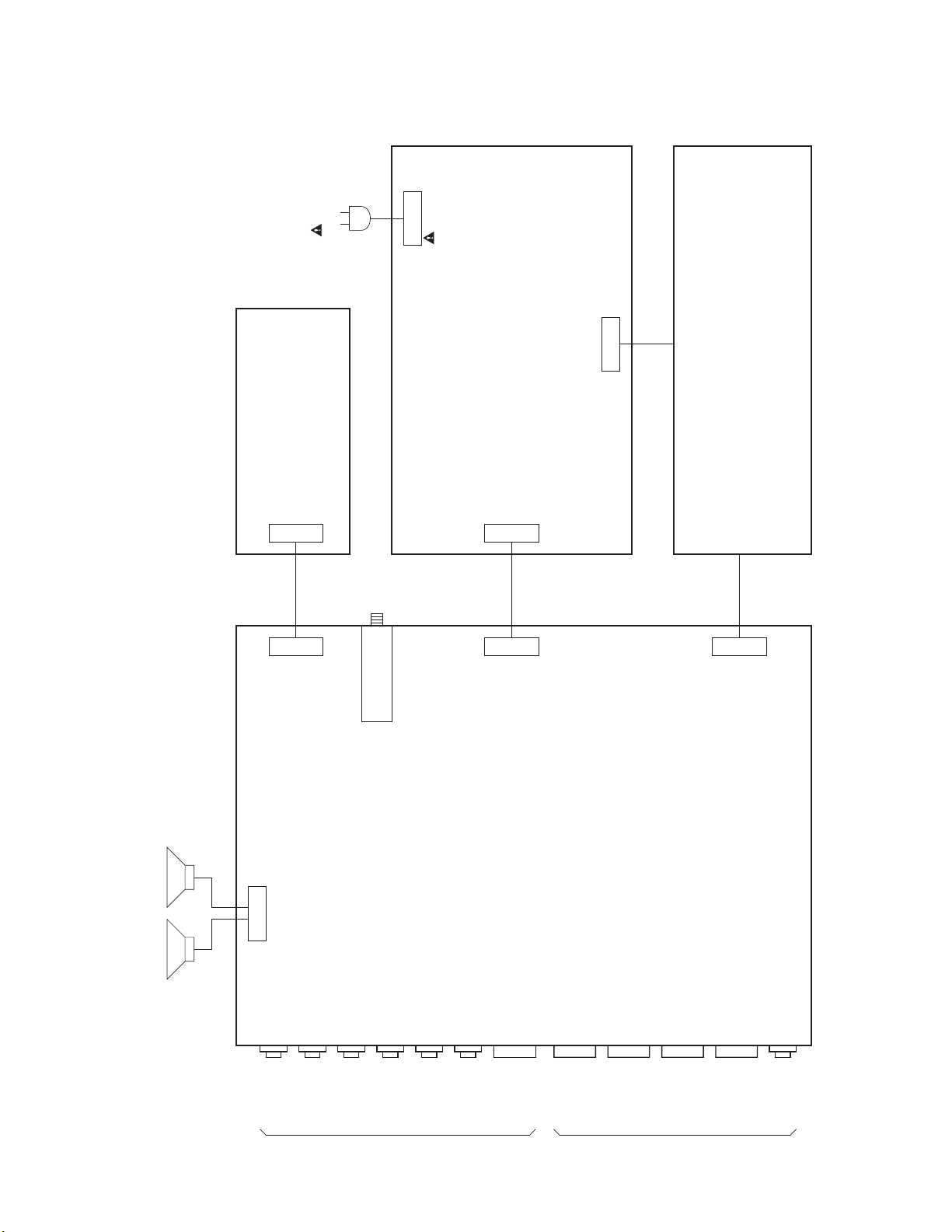
WIRING DIAGRAM
9
CN4001
1
CN3101
FUNCTION CBA
CL3101
1
9
AC CORD
CN601
12
1
CN631
1
CN3701
CL3701
CL1001
CN1001
17
LCD PANEL ASSEMBLY
23
CL3006
1
23
CN3006
30
SP3802
SPEAKER
SP3801
SPEAKER
R-CH
L-CH
CL3801
CN3801
14
COMPONENT
-Y/VIDEO-IN
COMPONENT
-Pb-IN
TUNER UNIT
COMPONENT
-Pr-IN
AUDIO(L)-IN
AUDIO(R)-IN
DIGITAL
AUDIO-OUT
(COAXIAL)
DIGITAL MAIN CBA UNIT POWER SUPPLY CBA
HDMI-
CONNECTOR-1
HDMI-
CONNECTOR-2
HDMI-
CONNECTOR-3
PC-RGB-IN
USB JACK
HEADPHONE
JACK
REAR
SIDE
PL12.6AWI11-1
Page 48
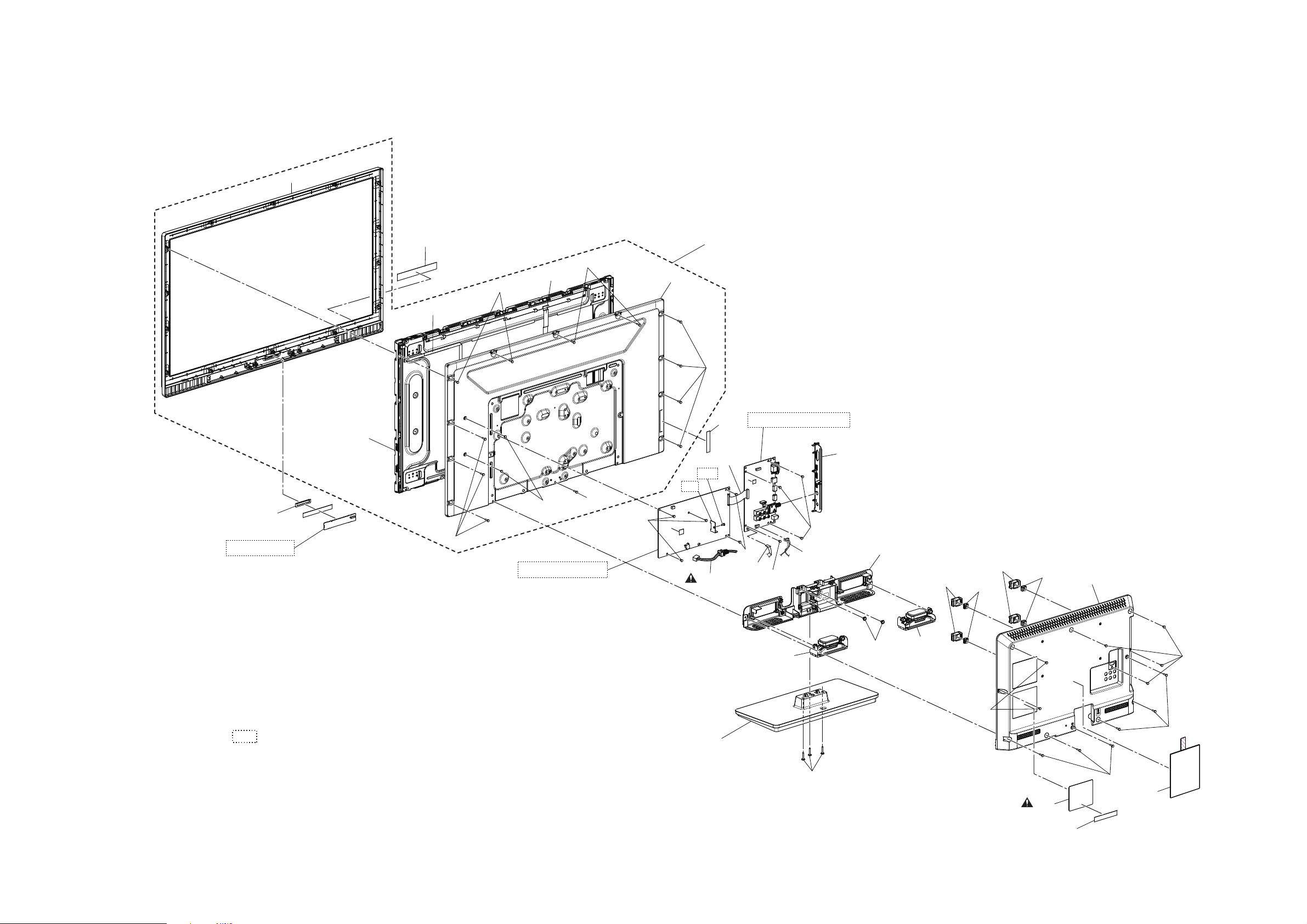
SSK1
A10
Stand Assembly
L14
L28
SP3801
SP3802
S7
L4
L4
L14
A3
B17
B17
B18
B18
B9
A14
L13
L13
L13
L13
CL3101
CL3701
CL3801
B3
S7
L23
L4
L4
L51
L4
A9
A20
L4
CL3006
CL1001
LCD Module
L4
A2
A18
See Electrical Parts List
for parts with this mark.
Digital Main CBA Unit
Power Supply CBA
Function CBA
AC601
LCD1
A1
X6
EXPLODED VIEWS
12-1 PL12.6-A_CEX
Page 49
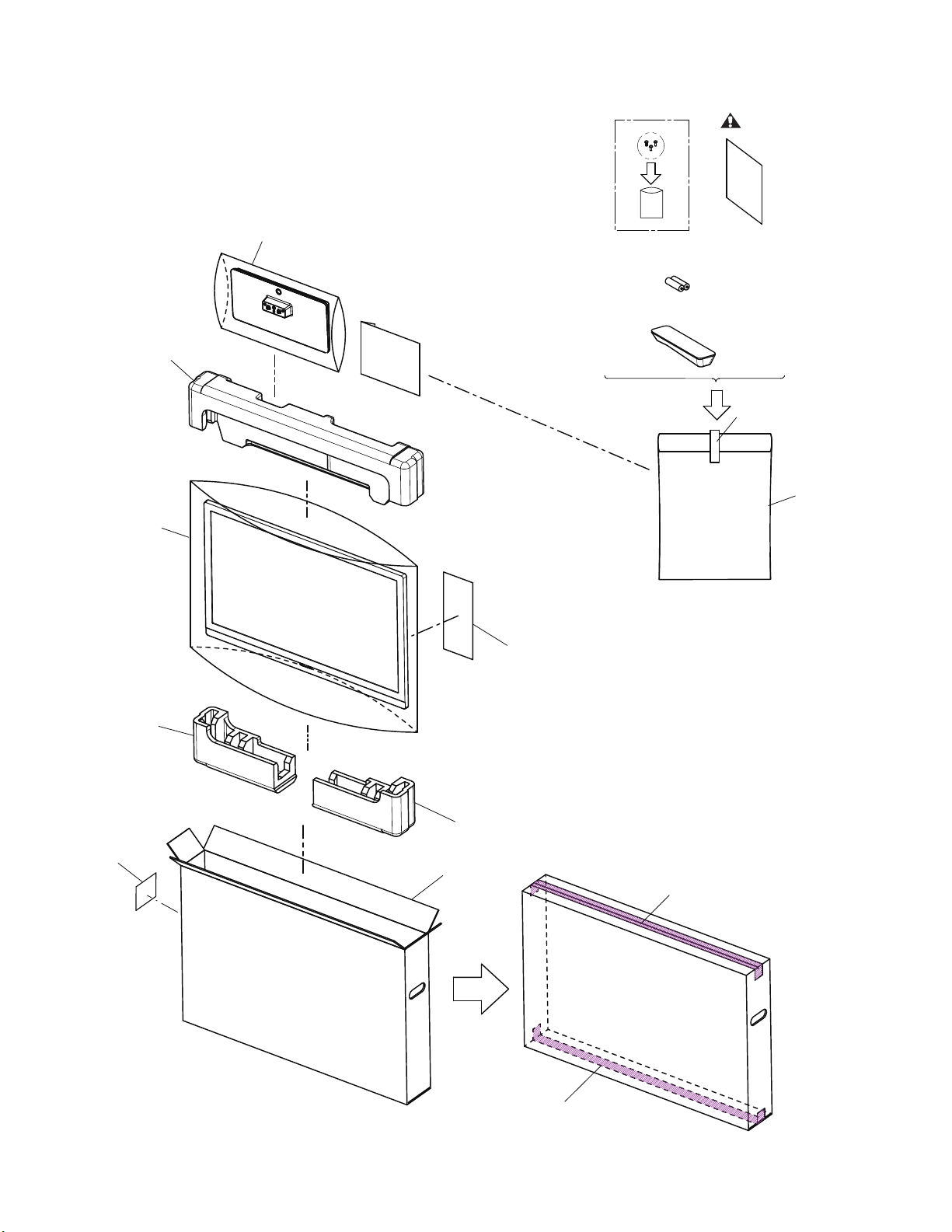
Packing
FRONT
FRONT
Packing Tape
Packing Tape
Packing Tape
Some Ref. Numbers are
not in sequence.
Tape
S13
S4
S4
S1
S6
S3
SSK1
X1
X4
X3
A10
X2
12-2 PL12.6-A_PEX
Page 50
PARTS LIST
Mechanical Parts
PRODUCT SAFETY NOTE: Products marked with a
# have special characteristics important to safety.
Before replacing any of these components, read
carefully the product safety notice in this service
manual. Don't degrade the safety of the product
through improper servicing.
NOTE: Parts that are not assigned part numbers
(---------) are not available.
Ref. No. Description Part No.
A3 REAR COVER A21FKZA 1EM127553
A9 SENSOR LENS A2170UT 1EM332157
A10 STAND ASSEMBLY A21F0UH 1EM029048
A14 JACK HOLDER A21F0UH 1EM226823
A18# RATING LABEL A21FLZA ---------A20 LOGO LABEL A21T7ZA ---------AC601# AC CORD W/O A GND WIRE UL/CSA/1700/NO/
B9 STAND HOLDER A21F0UH 1EM028669
B17 WALL MOUNT BRACKET A11N0UH 1EM434637
B18 WALL MOUNT COVER A2170UT 1EM332137
CL3101 FFC WIRE ASSEMBLY 9PIN 9PIN/WHITE/
CL3701 FFC WIRE ASSEMBLY 23PIN 23PIN/WHITE/
CL3801 WIRE ASSEMBLY 4PIN 4PIN/290MM&65MM WX1A21F0-309
L4 SCREW P-TIGHT 3X12 BIND HEAD+ BLK GBHP3120
L13 SCREW S-TIGHT M3X6 BIND HEAD+ GBJS3060
L14 S-TIGHT SCREW M3X6 BIND HEAD+BLACK GBHS3060
L28 DOUBLE SEMS SCREW M4X8+BLK M4X8
SP3801 SPEAKER MAGNETIC 8OHM/10W S0313F17 DS08100XQ001
SP3802 SPEAKER MAGNETIC 8OHM/10W S0313F17 DS08100XQ001
SSK1 STAND SCREW KIT A21F0UH
BLACK
143MM
80MM
BLACK
(SCREW P-TIGHT M4X14 BIND HEAD+BLK)
PAC K IN G
S1 CARTON A21FLZA 1EM439360
S3 STYROFOAM TOP A21F0UH 1EM029285
S4 STYROFOAM BOTTOM A21F0UH 1EM029286
S6 SET BAG A1AFDUH 1EM333990
S7 SERIAL NO. LABEL A01PBUH ---------S13 CARTON LABEL A21FLZA ----------
ACCESSORIES
X1 POLYETHYLENE BAG HDPE 180X340XT0.03 1EM435579
X2# OWNERS MANUAL A21FLZA 1EMN30060
X3 REMOTE CONTROL TRANSMITTER YKF259-
X4 BATTERY R03-B500/01S XB0M451CZB01
X6 QUICK START GUIDE A21FLZA 1EMN30059
001
WAC1720LW005
WX1A21F0-111
WX1A21F0-110
FPH34080
1ESA31009
URMT34JHG001
LCD PANEL ASSEMBLY
Ref. No. Description Part No.
LCD1 LCD PANEL ASSEMBLY
A1 FRONT CABINET A21FKZA 1EM227763
A2 REAR FRAME PAINT 1EM332238
CL1001 FFC 7PIN 7P/P1.0/470MM WX1U24F0-F03
CL3006 FFC 30PIN 30P/P0.5/210MM WX1U24F0-F01
L4 SCREW P-TIGHT 3X12 BIND HEAD+ BLK GBHP3120
L51 SCREW M3X4 M3X4 BIND+ (B-NI) SBH33040
Consists of the following
LCD MODULE ----------
U24F0P0
2011/12/19 13-1 A21FNZD.fm
Page 51
Electrical Parts
PRODUCT SAFETY NOTE: Products marked with a
# have special characteristics important to safety.
Before replacing any of these components, read
carefully the product safety notice in this service
manual. Don't degrade the safety of the product
through improper servicing.
NOTES:
1. Parts that are not assigned part numbers (---------)
are not available.
2. Tolerance of Capacitors and Resistors are noted
with the following symbols.
C.....±0.25% D.....±0.5% F.....±1%
G.....±2% J......±5% K.....±10%
M.....±20% N.....±30% Z.....+80/-20%
DIGITAL MAIN CBA UNIT
Ref. No. Description Part No.
DIGITAL MAIN CBA UNIT A21FLMMA-001
ICS
IC3001 IC DCDC CONVERTER MP2305SDS-LF-Z/
IC3002 IC DDR2-SDRAM K4T51163QI-HCF7 NSCA0R0SM022
IC3003 IC DCDC CONVERTER MP2305SDS-LF-Z/
IC3004 IC LDO REGULATOR BD00IC0WEFJ/HTSOP-J8QSCA0T0RM397
IC3005 IC DTV-C7V R8A05011BG-U0/256FHP QSAA0R0HT057
IC3006 32MBIT C-MOS SERIAL FLASH
IC3007 IC LDO REGULATOR BD00IC0WEFJ/HTSOP-J8QSCA0T0RM397
IC3008 IC DCDC CONVERTER MP2305SDS-LF-Z/
IC3009 IC RESET IC-PST8429UR QSCA0T0MM075
IC3011 IC EEPROM BU9883FV-WE2 QSCA0T0RM105
IC3013 IC SINGLE BUS BUFFER 74LVC1G126GW NSCA0TNXP004
IC3014 IC SINGLE BUS BUFFER 74LVC1G126GW NSCA0TNXP004
IC3018 IC HDMI SW BU16029KV-E2 QSCA0T0RM223
IC3019 HIGH-SIDE SWITCH IC BD2224G-TR/SSOP5/ 5PQSCA0T0RM011
IC3801 IC D-CLASS POWER AMPLIFER R2A15122FP-
SOIC8
SOIC8
S25FL032P0XMFI010 /S
SOIC8
W00R/HQFP
NSCA0T09M010
NSCA0T09M010
QSCA0R0FJ008
NSCA0T09M010
QSCA0T0HT005
TUNER
TU3901 TUNER UNIT U9001UH U9001UH
POWER SUPPLY CBA
Ref. No. Description Part No.
POWER SUPPLY CBA
Consists of the following
CAPACITORS
C501 CHIP CERAMIC CAP.(1608) F Z 0.1μF/50V CHD1JZ30F104
C602# SAFTY CAP. 1000pF/250V KX CA2E102MR101
C603# SAFTY CAP. 1000pF/250V KX CA2E102MR101
C604# CAP METALIZED FILM 0.22μF/275V/K CTA224PKR001
C605 CAP ELE 330μF/200V/M/87 CEB3310S6016
C606 CERAMIC CAP. 820pF/2KV CA3D821PAN04
A21F0MPW-003
Ref. No. Description Part No.
C607 CHIP CERAMIC CAP. B K 1200pF/50V CHD1JK30B122
C608 CHIP CERAMIC CAP. B K 0.039μF/50V CHD1JK30B393
C609# CHIP CER. BK 0.082μF/50V CHD1JK30B823
C610 CHIP CERAMIC CAP.(1608) B K 1000pF/50V CHD1JK30B102
C614# CAP METALIZED FILM 0.22μF/275V/K CTA224PKR001
C616# SAFTY CAP. 1000pF/250V KX CA2E102MR101
C650 CAP CERAMIC HV 2200pF/1KV B K CA3A222TE006
C651 CAP ELE 470μF/25V/M/85 CED4710V8006
C652 CAP ELE 470μF/25V/M/85 CED4710V8006
C653 CAP ELE 470μF/25V/M/85 CED4710V8006
C654 CAP ELE 470μF/35V/M/85 CEE4710V8006
C655 CAP ELE 470μF/35V/M/85 CEE4710V8006
C656 CAP ELE 1μF/50V/M/85 CEF1R00V8006
C660 CHIP CERAMIC CAP.(1608) B K 0.1μF/50V CHD1JK30B104
C663 CAP ELE 100μF/10V/M/85 CEB1010V8006
C665 CHIP CERAMIC CAP.(1608) B K 0.1μF/50V CHD1JK30B104
C1001 CAP ELE 330μF/25V/M/85 CED3310V8006
C1003 CHIP CERAMIC CAP.(1608) B K 1μF/25V CHD1EK30B105
C1004 CHIP CERAMIC CAP.(1608) B K 1μF/25V CHD1EK30B105
C1006 CHIP CERAMIC CAP.(1608) B K 1000pF/50V CHD1JK30B102
C1007 CERAMIC CAP. 220pF/1KV CCD3AKN0B221
C1008 CHIP CERAMIC CAP.(3216) X7R K 1.0μF/100V CA2A105MR080
C1009 CHIP CERAMIC CAP.(3216) X7R K 1.0μF/100V CA2A105MR080
C1010 CAP ELE 47μF/100V/M/85 CEH4700V8006
C1011 CAP ELE 47μF/100V/M/85 CEH4700V8006
C1012 CHIP CERAMIC CAP.(3216) X7R K 1.0μF/100V CA2A105MR080
C1014 CHIP CERAMIC CAP.(1608) B K 1000pF/50V CHD1JK30B102
C1016 CHIP CERAMIC CAP.(1608) B K 1μF/25V CHD1EK30B105
C1017 CHIP CERAMIC CAP.(1608) F Z 0.1μF/50V CHD1JZ30F104
C1019 CHIP CERAMIC CAP.(1608) B K 4.7μF/6.3V CHD0KK30B475
CONNECTORS
CN601# CONNECTOR S2P3-VH (LF)(SN) JCVHC02JG002
CN631 FFC CONNECTOR IMSA-9615S-23A-PP-A JC96J23ER007
CN1001 FPC/FFC CONNECTOR IMSA-9615S-07A-PP-AJC96J07ER007
DIODES
D102A DIODE SWITCHING HSC119 TRF -E QD1Z00HSC119
D401A DIODE SWITCHING HSC119 TRF -E QD1Z00HSC119
D402 ZENER DIODE SMD TFZGTR24B QD1B000TFZ24
D501 DIODE ZENER SMD UDZSNPTE-1733B QD1B0UDZNP33
D502 DIODE ZENER SMD UDZSNPTE-1730B QD1B0UDZNP30
D601 DIODE 1N5406BH NDL1001N5406
D602 DIODE 1N5406BH NDL1001N5406
D603 DIODE 1N5406BH NDL1001N5406
D604 DIODE 1N5406BH NDL1001N5406
D605 ZENER DIODE MM5Z4V3B ND1BMM5Z4V3B
D607# DIODE ZENER 1ZB27BB NDWZ0001ZB27
D608# DIODE ZENER 1ZB36BB NDWZ0001ZB36
D609A# DIODE SWITCHING HSC119 TRF -E QD1Z00HSC119
D610A DIODE SWITCHING HSC119 TRF -E QD1Z00HSC119
D650 DIODE SCHOTTKY SB3150BH NDWZ00SB3150
D651 DIODE SCHOTTKY SB3150BH NDWZ00SB3150
D653 DIODE SHOTTKY SB3200BR NDWZ3200D027
D654# DIODE ZENER 1ZB30BB NDWZ0001ZB30
D656 DIODE FAST RECOVERY RS1BJTB ND1Z0RS1BJTB
D657 ZENER DIODE MM5Z5V6B ND1BMM5Z5V6B
D660 IC SHUNT REGULATOR SL431A-AT NSZBA0TAUK01
D661 DIODE ZENER SMD PZU5.6B2.115 ND1200PZU5R6
D662 IC SHUNT REGULATOR SL431A-AT NSZBA0TAUK01
D1001 DIODE SCHOTTKY SMD SK210TD ND1Z0SK210TD
2012/09/12 13-2 A21FNEL.fm
Page 52
Ref. No. Description Part No.
ICS
IC601# IC PHOTOCOUPLER TLP781F(D4-FUNBLL F) QPEL781FBLLF
IC1001# IC LED BACKLIGHT CONTROLLER HA7209PC
/SOP /24PIN
NSCA0T00H003
COILS
L601# COIL LINE FILTER JLB20154/18MH LLEG0Z0XB022
L602# COIL LINE FILTER JLB20154/18MH LLEG0Z0XB022
L1001 POWER INDUCTORS CWKBNP-220K LLF2200KV002
TRANSISTORS
Q501# FET 2SK3498(T6L1FUNANQ QF1Z02SK3498
Q601# FET MOS TK8A50D(LS1FND3 QM QEE1TK8A50DM
Q602# TRANSISTOR 2SC2120-Y(TE2 F T) QQSY2SC2120F
Q650 CHIP TRANSISTOR KTC3875S-Y-RTK/P NQ1YKTC3875S
Q652 CHIP TRANSISTOR KTC3875S-Y-RTK/P NQ1YKTC3875S
Q653 CHIP TRANSISTOR KTC3875S-Y-RTK/P NQ1YKTC3875S
Q656 TRANSISTOR 2SC2120-Y(TE2 F T) QQSY2SC2120F
Q1001# FET MOS SMD AP18T10AGH-HF NF2Z18T10AGH
RESISTORS
R401 RES CHIP 1608 1/10W J 8.2k Ω RRXA822HH013
R402 RES CHIP 1608 1/10W J 3.0k Ω RRXA302HH013
R501# METAL OXIDE FILM RES. 2W J 47 Ω RN02470ZU001
R502 RES CHIP 1608 1/10W J 1.5M Ω RRXA155HH013
R601# RES. CARBON FILM J 1/2W J 1.2M Ω RCX2125T1003
R602 RES CEMENT 5W/J/1.2 Ω RWJ1R2PAK007
R603 RES CHIP 3216 1/4W J 330k Ω RRX4334HH034
R604 RES CHIP 3216 1/4W J 330k Ω RRX4334HH034
R605 RES CHIP 3216 1/4W J 330k Ω RRX4334HH034
R606 RES CARBON FILM T 1/4W J 270 Ω RCX4271T1001
R607 RES CARBON FILM T 1/4W J 270 Ω RCX4271T1001
R608 RES CARBON FILM T 1/4W J 1.5k Ω RCX4152T1001
R611# METAL OXIDE RES. 2W J 0.36 Ω RN02R36ZU001
R612 RES CARBON FILM T 1/4W J 2.2k Ω RCX4222T1001
R613 RES CARBON FILM T 1/4W J 220 Ω RCX4221T1001
R614 RES CHIP 3216 1/4W J 330k Ω RRX4334HH034
R650 RES CARBON FILM T 1/4W J 5.6k Ω RCX4562T1001
R651# RES CHIP 1608 1/10W J 1.0 Ω RRXA1R0HH013
R652 RES CHIP 1608 1/10W F 56.0k Ω RTW5602HH008
R653 RES CHIP 1608 1/10W F 22.0k Ω RTW2202HH008
R654 RES CARBON FILM T 1/4W J 180 Ω RCX4181T1001
R655 RES CARBON FILM T 1/4W J 180 Ω RCX4181T1001
R657 RES CARBON FILM T 1/4W J 3.9k Ω RCX4392T1001
R658 RES CHIP 1608 1/10W J 2.7k Ω RRXA272HH013
R659 RES CHIP 1608 1/10W F 22.0k Ω RTW2202HH008
R660 RES CHIP 1608 1/10W F 2.70k Ω RTW2701HH008
R661 RES CHIP 1608 1/10W F 3.30k Ω RTW3301HH008
R662 RES CHIP 1608 1/10W F 3.30k Ω RTW3301HH008
R663 RES CHIP 1608 1/10W J 47k Ω RRXA473HH013
R664 RES CHIP 1608 1/10W J 10k Ω RRXA103HH013
R665 RES CHIP 1608 1/10W J 10k Ω RRXA103HH013
R668 RES CHIP 1608 1/10W J 22k Ω R
R669 RES CHIP 1608 1/10W J 10k Ω RRXA103HH013
R670 RES CARBON FILM T 1/4W J 1.0k Ω RCX4102T1001
R671 RES CARBON FILM T 1/4W J 1.0k Ω RCX4102T1001
R672 WIRE CP STP-S-0.50 XZ40F0REN001
R673# RES CHIP 1608 1/10W J 5.6 Ω RRXA5R6HH013
R677 RES CHIP 1608 1/10W J 10k Ω RRXA103HH013
R678 RES CARBON FILM T 1/4W J 5.6k Ω RCX4562T1001
R680 RES CHIP 1608 1/10W J 100 Ω RRXA101HH013
R681 RES CHIP 1608 1/10W F 10.0k Ω RTW1002HH008
R682 RES CHIP 1608 1/10W 0 Ω RRXA000HH014
R1001 RES CHIP 1608 1/10W J 10 Ω RRXA100HH013
R1002 RES CHIP 1608 1/10W J 200 Ω RRXA201HH013
R1003# METAL OXIDE RES. 1W J 0.18 Ω RN01R18ZU001
RXA223HH013
Ref. No. Description Part No.
R1004 RES CHIP 1608 1/10W F 560k Ω RTW5603HH008
R1005 RES CHIP 1608 1/10W F 200k Ω RTW2003HH008
R1006 RES CHIP 1608 1/10W F 27.0k Ω RTW2702HH008
R1007 RES CHIP 1608 1/10W F 100k Ω RTW1003HH008
R1008 RES CHIP 1608 1/10W F 360 Ω RTW3600HH008
R1009 RES CHIP 1608 1/10W F 8.20k Ω RTW8201HH008
R1010 RES CHIP 1608 1/10W J 10k Ω RRXA103HH013
R1011 RES CHIP 1608 1/10W J 100k Ω RRXA104HH013
R1012 RES CHIP 1608 1/10W F 100 Ω RTW1000HH008
R1014 RES CHIP 1608 1/10W J 240 Ω RRXA241HH013
R1015 RES CHIP 1608 1/10W J 240 Ω RRXA241HH013
R1016 RES CHIP 1608 1/10W J 10k Ω RRXA103HH013
R1017 RES CHIP 1608 1/10W J 100k Ω RRXA104HH013
R1018 RES CHIP 1608 1/10W 0 Ω RRXA000HH014
R1020 RES CHIP 1608 1/10W 0 Ω RRXA000HH014
R1021 RES CHIP 1608 1/10W 0 Ω RRXA000HH014
R1502 RES CHIP 1608 1/10W 0 Ω RRXA000HH014
R1503 RES CHIP 1608 1/10W 0 Ω RRXA000HH014
MISCELLANEOUS
B3 HEAT SINK PNI A11N5UH 1EM435557
BC601 BEADS INDUCTOR FBR07HA121SB-00 LLBF00STU030
BC602 BEADS INDUCTOR FBR07HA121SB-00 LLBF00STU030
BC603 BEADS INDUCTOR FBR07HA121SB-00 LLBF00STU030
BC1002 WIRE CP STP-S-0.50 XZ40F0REN001
F601# FUSE STC4A125V U/CT PAGE20CW3402
FH601 FUSE HOLDER MSF-015-RS-SN (B110) XH001Z0LY001
FH602 FUSE HOLDER MSF-015-RS-SN (B110) XH001Z0LY001
JS632 WIRE CP STP-S-0.50 XZ40F0REN001
L23 SCREW B-TIGHT D3X8 BIND HEAD+ GBJB3080
SA601# SURGE ABSORBER 470V+-10PER NVQZ10D471KB
T601# TRANS POWER BCK-28DZ LTT2PCMEK036
FUNCTION CBA
Ref. No. Description Part No.
FUNCTION CBA
Consists of the following
CAPACITORS
C4001 CHIP CERAMIC CAP.(1005) B K 1μF/6.3V CHB0KK30B105
C4002 CHIP CERAMIC CAP.(1005) B K 2200pF/50V CHB1JK30B222
C4051 CHIP CERAMIC CAP.(2125) B K 10μF/6.3V CHE0KK30B106
C4052 CHIP CERAMIC CAP.(1005) B K 1000pF/50V CHB1JK30B102
C4053 CHIP CERAMIC CAP.(1005) F Z 0.1μF/16V CHB1CZ30F104
C4054 CHIP CERAMIC CAP.(1005) F Z 0.1μF/16V CHB1CZ30F104
C4056 CHIP CERAMIC CAP.(2125) B K 10μF/6.3V CHE0KK30B106
CONNECTOR
CN4001 FFC CONNECTOR 9P 9611S-09Y916 JC96D09ER014
DIODES
D4001 ZENER DIODE MM5Z5V6B ND1BMM5Z5V6B
D4003 ZENER DIODE MM5Z5V6B ND1BMM5Z5V6B
D4004 ZENER DIODE MM5Z5V6B ND1BMM5Z5V6B
D4051 LED WHITE SMD SMLE12WBC7W1HR QP1HWBC7W1HR
IC
IC4001 IC TOUCHSENSOR MICON NON-AUTOT
CY8C20324-12LQXIT/CP
RESISTORS
R4001 CHIP RES. 1/16W J 560 Ω RRXG561HH004
R4002 CHIP RES. 1/16W J 560 Ω RRXG561HH004
R4003 CHIP RES. 1/16W J 560 Ω RRXG561HH004
R4004 CHIP RES. 1/16W J 560 Ω RRXG561HH004
R4005 CHIP RES. 1/16W J 560 Ω RRXG561HH004
R4006 CHIP RES. 1/16W J 560 Ω RRXG561HH004
R4007 CHIP RES. 1/16W J 560 Ω RRXG561HH004
A21FLMSW-001
NSCA0T0TY080
2012/09/12 13-3 A21FNEL.fm
Page 53
Ref. No. Description Part No.
R4008 RES CHIP 1005 1/16W J 18k Ω RRXG183HH004
R4009 CHIP RES.(1005) 1/16W J 8.2k Ω RRXG822HH004
R4010 CHIP RES. 1/16W J 4.7k Ω RRXG472HH004
R4011 CHIP RES.(1005) 1/16W J 2.7k Ω RRXG272HH004
R4012 CHIP RES.(1005) 1/16W J 2.2k Ω RRXG222HH004
R4013 CHIP RES.(1005) 1/16W J 100 Ω RRXG101HH004
R4014 CHIP RES.(1005) 1/16W J 2.2k Ω RRXG222HH004
R4021 CHIP RES. 1/16W J 10 Ω RRXG100HH004
R4022 CHIP RES. 1/16W J 10 Ω RRXG100HH004
R4051 CHIP RES. 1/16W J 56 Ω RRXG560HH004
R4052 RES CHIP 1005 1/16W J 6.8k Ω RRXG682HH004
R4053 CHIP RES. 1/16W J 4.7k Ω RRXG472HH004
R4054 CHIP RES.(1005) 1/16W J 1k Ω RRXG102HH004
R4062 CHIP RES.(1005) 1/16W 0 Ω RRXG000HH005
MISCELLANEOUS
RS4051 SENSOR REMOTE RECEIVER GP1USC32XP USEJRS0SH004
2012/09/11 13-4 A21FNEL.fm
Page 54

REVISION HISTORY
Chassis PL12.6
• 2012/8/18 32PFL2507/F8 (Serial No.: VM1) added
14-1 PL12.6REV
Page 55

COMPARISON LIST OF MODEL NAMES
Chassis PL12.6
32PFL2507/F8 (VM1) A21FNZD
15-1 PL12.6COM
 Loading...