

Page 1
Colour Television Chassis
18810_000_090925.eps
091012
TPH1.1A
LA
Contents Page Contents Page
1. Revision List 2
2. Technical Specifications, Connections, and Chassis
Overview 2
3. Precautions, Notes, and Abbreviation List 5
4. Mechanical Instructions 9
5. Service Modes, Error Codes, and Fault Finding 14
6. Alignments 17
7. Circuit Descriptions 18
8. IC Data Sheets 22
9. Block Diagrams
Wiring Diagram 32" 29
Wiring Diagram 42" 30
Wiring Diagram 47" 31
Block Diagram Audio and Video 32
Block Diagram Power Diagram 33
10. Circuit Diagrams and PWB Layouts Drawing PWB
Power Board Power, 32"
Power Board Inverter, 32" (A02) 35 36-36
Power Board AC Side, 42" (A01)37 42-43
Power Board Inverter Control, 42" (A02)38 42-43
Power Board Main Power, 42" (A03)39 42-43
Power Board PFC, 42" (A04)40 42-43
Power Board Stand-by, 42" (A05) 41 42-43
Inverter Board Inverter, 32" (A01)44 45-46
Inverter Board Inverter, 42" (A01)47 48-49
Adapter Board Adapter, 47" (A01)50 51-52
SSB: Power (B01) 53 63-72
SSB: HDMI (B02) 54 63-72
SSB: Tuner (B03)55 63-72
SSB: VGA & YPbPr Connectors (B04)56 63-72
SSB: SV & AV (B05)57 63-72
SSB: M2B HDMI & Analog I / O (B06)58 63-72
SSB: M2B Audio (B07)59 63-72
SSB: M2B MCU (B08)60 63-72
©
Copyright 2009 Koninklijke Philips Electronics N.V.
All rights reserved. No part of this publication may be reproduced, stored in a
retrieval system or transmitted, in any form or by any means, electronic, mechanical,
photocopying, or otherwise without the prior permission of Philips.
(A01)34 36-36
SSB: M2B LVDS (B09)61 63-72
SSB: Component 2 & USB Input (B10)62 63-72
IR Board 32" (J)73 74
IR Board 42" and 47" (J)75 76
Keyboard Control Panel (E) 77 78
Published by DoZ/JY 0972 BU TV Consumer Care Printed in the Netherlands Subject to modification EN 3122 785 18811
2009-Dec-18
Page 2
EN 2 TPH1.1A LA1.
1. Revision List
Revision List
Manual xxxx xxx xxxx.0
• First release.
Manual xxxx xxx xxxx.1
• Added 47PFL1609/93 set to the manual.
• Chapter 2: Added Model number to Table 2-1
• Chapter 4: Added cable dressing diagram.
• Chapter 5: Added factory menu explanation.
• Chapter 7: Updated the circuit descriptions.
• Chapter 9: Added wiring diagram.
• Chapter 10: Added power board diagram and PWB
layouts.
.
2. Technical Specifications, Connections, and Chassis Overview
Index of this chapter:
2.1 Technical Specifications
2.2 Directions for Use
2.3 Connections
2.4 Chassis Overview
Notes:
• Figures can deviate due to the different set executions.
• Specifications are indicative (subject to change).
2.1 Technical Specifications
For on-line product support please use the links in Table 2-1.
Here is product information available, as well as getting started,
user manuals, frequently asked questions and software &
drivers.
Table 2-1 Described Model Numbers:
Model Number Styling Published in
32PFL1409/
42PFL1609/93
47PFL1609/93 3122 785 18811
Note: The given Model Numbers are subject to change.
93
M2B
3122 785 18810
2.2 Directions for Use
Directions for use can be downloaded from the following
websites:
http://www.philips.com/support
http://www.p4c.philips.com
2009-Dec-18
Page 3
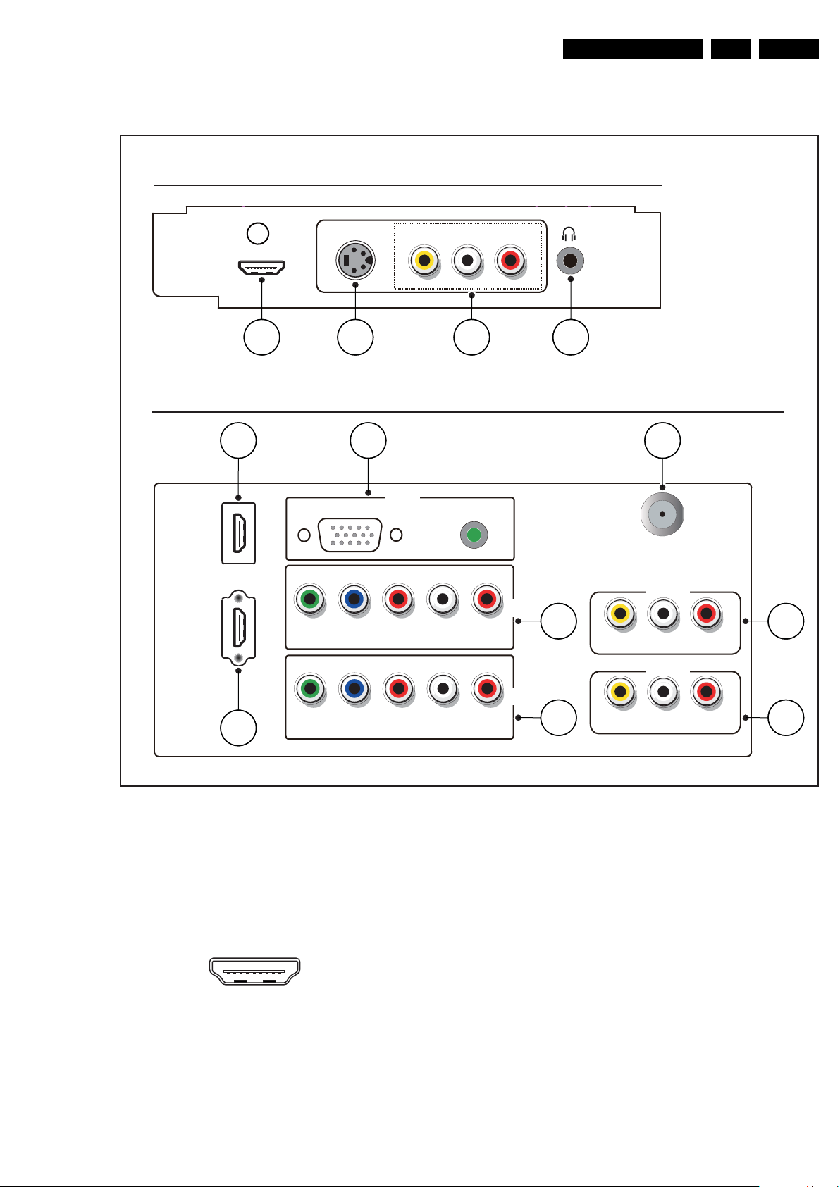
Technical Specifications, Connections, and Chassis Overview
S-VIDEO VIDEO
L -AUDIO -R
HDMI3
HDMI 1
VGA
AUDIO
TV ANTENNA
YPrLRPb
HDMI 2
YPrLRPb
VIDEO L R
PC IN
EXT1
EXT2
AV OUT
AV IN
VIDEO
LR
19
1
18 2
19
1
18 2
19
1
18 2
18810_001_090925.eps
091215
Side Connectors
Rear Connectors
1
5 7
8
9
11
12
10
6
2 3 4
10000_017_090121.eps
090428
19
1
18 2
2.3 Connections
EN 3TPH1.1A LA 2.
Note: The following connector colour abbreviations are used:
Bk = Black, Bu = Blue, Gn = Green, Gy = Grey, Rd = Red,
Wh = White, Ye = Yellow.
2.3.1 Side Connections
1 - HDMI 3: Digital Video, Digital Audio - In
1 -D2+ Data channel j
2 -Shield Gnd H
3 -D2- Data channel j
4 -D1+ Data channel j
5 -Shield Gnd H
6 -D1- Data channel j
Figure 2-2 HDMI (type A) connector
Figure 2-1 Connection overview
7 -D0+ Data channel j
8 -Shield Gnd H
9 -D0- Data channel j
10 - CLK+ Data channel j
11 - Shield Gnd H
12 - CLK- Data channel j
13 - Easylink Control channel jk
14 - n.c.
15 - DDC_SCL DDC clock j
16 - DDC_SDA DDC data jk
17 - Ground Gnd H
18 - +5V j
19 - HPD Hot Plug Detect j
20 - Ground Gnd H
2009-Dec-18
Page 4
EN 4 TPH1.1A LA2.
1
6
10
11
5
15
10000_002_090121.eps
090127
Technical Specifications, Connections, and Chassis Overview
2 - S-Video (Hosiden): Video Y/C - In
1 -Ground Y Gnd H
2 -Ground C Gnd H
3 -Video Y 1 V
4 -Video C 0.3 V
/ 75 Ω j
PP
/ 75 Ω j
PP
3 - Cinch: Video CVBS - In, Audio - In
Rd -Audio R 0.5 V
Wh -Audio L 0.5 V
Ye - Video CVBS 1 V
/ 10 kΩ jq
RMS
/ 10 kΩ jq
RMS
/ 75 Ω jq
PP
4 - Head phone (Output)
Bk -Head phone 32 - 600 Ω / 10 mW ot
2.3.2 Rear Connections
5, 6 - HDMI 1 & 2: Digital Video, Digital Audio - In
See 1 - HDMI 3: Digital Video, Digital Audio - In
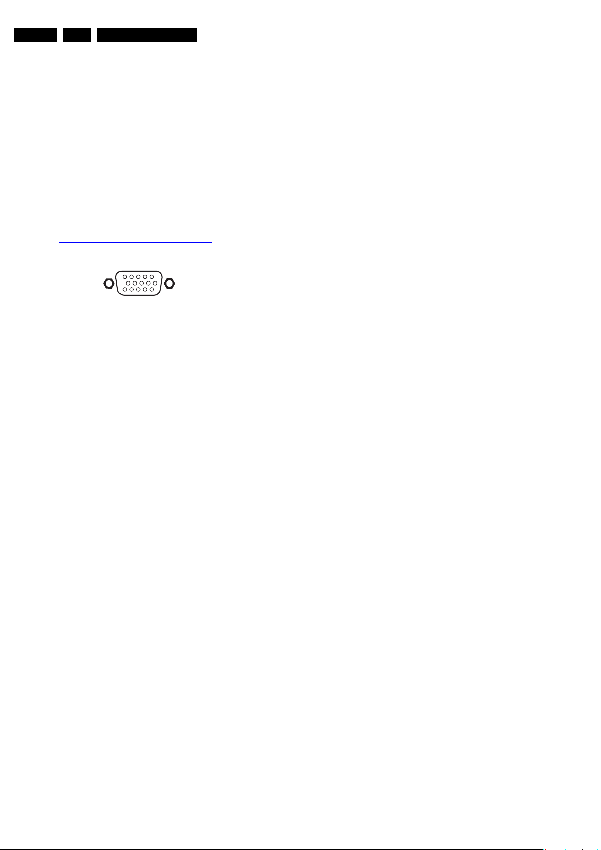
7 - VGA: Video RGB - In
Figure 2-3 VGA Connector
1 -Video Red 0.7 V
2 -Video Green 0.7 V
3 -Video Blue 0.7 V
4-n.c.
/ 75 Ω j
PP
/ 75 Ω j
PP
/ 75 Ω j
PP
5 -Ground Gnd H
6 -Ground Red Gnd H
7 -Ground Green Gnd H
8 -Ground Blue Gnd H
9-+5V
10 - Ground Sync Gnd H
+5 V j
DC
11 - n.c.
12 - DDC_SDA DDC data j
13 - H-sync 0 - 5 V j
14 - V-sync 0 - 5 V j
15 - DDC_SCL DDC clock j
7 - VGA Audio - In
Bk -VGA Audio 32 - 600 Ω / 10 mW j
8, 9 - EXT1 & 2: Cinch: Video YPbPr - In, Audio - In
Gn - Vid eo Y 1 V
Bu - Video Pb 0.7 V
Rd -Video Pr 0.7 V
.
Rd -Audio - R 0.5 V
Wh -Audio - L 0.5 V
/ 75 Ω jq
PP
/ 75 Ω jq
PP
/ 75 Ω jq
PP
/ 10 kΩ jq
RMS
/ 10 kΩ jq
RMS
10 - Aerial - In
- -IEC-type (EU) Coax, 75 Ω D
11 - Cinch: Video CVBS - Out, Audio - Out
Ye - Video CVBS 1 V
Wh -Audio L 0.5 V
Rd -Audio R 0.5 V
/ 75 Ω kq
PP
/10 kΩ kq
RMS
/ 10 kΩ kq
RMS
12 - Cinch: Video CVBS - In, Audio - In
Ye - Video CVBS 1 V
Wh -Audio L 0.5 V
Rd -Audio R 0.5 V
/ 75 Ω jq
PP
/ 10 kΩ jq
RMS
/ 10 kΩ jq
RMS
2.4 Chassis Overview
Refer to chapter 9. Block Diagrams for PWB/CBA locations.
2009-Dec-18
Page 5

Precautions, Notes, and Abbreviation List
3. Precautions, Notes, and Abbreviation List
EN 5TPH1.1A LA 3.
Index of this chapter:
3.1 Safety Instructions
3.2 Warnings
3.3 Notes
3.4 Abbreviation List
3.1 Safety Instructions
Safety regulations require the following during a repair:
• Connect the set to the Mains/AC Power via an isolation
transformer (> 800 VA).
• Replace safety components, indicated by the symbol h,
only by components identical to the original ones. Any
other component substitution (other than original type) may
increase risk of fire or electrical shock hazard. Of de set
ontploft!
Safety regulations require that after a repair, the set must be
returned in its original condition. Pay in particular attention to
the following points:
• Route the wire trees correctly and fix them with the
mounted cable clamps.
• Check the insulation of the Mains/AC Power lead for
external damage.
• Check the strain relief of the Mains/AC Power cord for
proper function.
• Check the electrical DC resistance between the Mains/AC
Power plug and the secondary side (only for sets that have
a Mains/AC Power isolated power supply):
1. Unplug the Mains/AC Power cord and connect a wire
between the two pins of the Mains/AC Power plug.
2. Set the Mains/AC Power switch to the “on” position
(keep the Mains/AC Power cord unplugged!).
3. Measure the resistance value between the pins of the
Mains/AC Power plug and the metal shielding of the
tuner or the aerial connection on the set. The reading
should be between 4.5 MΩ and 12 MΩ.
4. Switch “off” the set, and remove the wire between the
two pins of the Mains/AC Power plug.
• Check the cabinet for defects, to prevent touching of any
inner parts by the customer.
picture carrier at 475.25 MHz for PAL, or 61.25 MHz for
NTSC (channel 3).
• Where necessary, measure the waveforms and voltages
with (D) and without (E) aerial signal. Measure the
voltages in the power supply section both in normal
operation (G) and in stand-by (F). These values are
indicated by means of the appropriate symbols.
3.3.2 Schematic Notes
• All resistor values are in ohms, and the value multiplier is
often used to indicate the decimal point location (e.g. 2K2
indicates 2.2 kΩ).
• Resistor values with no multiplier may be indicated with
either an “E” or an “R” (e.g. 220E or 220R indicates 220 Ω).
• All capacitor values are given in micro-farads (μ=× 10
nano-farads (n =× 10
• Capacitor values may also use the value multiplier as the
decimal point indication (e.g. 2p2 indicates 2.2 pF).
• An “asterisk” (*) indicates component usage varies. Refer
to the diversity tables for the correct values.
• The correct component values are listed on the Philips
Spare Parts Web Portal.
3.3.3 Spare Parts
For the latest spare part overview, consult your Philips Spare
Part web portal.
3.3.4 BGA (Ball Grid Array) ICs
Introduction
For more information on how to handle BGA devices, visit this
URL: http://www.atyourservice-magazine.com
“Magazine”, then go to “Repair downloads”. Here you will find
Information on how to deal with BGA-ICs.
BGA Temperature Profiles
For BGA-ICs, you must use the correct temperature-profile.
Where applicable and available, this profile is added to the IC
Data Sheet information section in this manual.
-9
), or pico-farads (p =× 10
. Select
-12
-6
),
).
3.2 Warnings
• All ICs and many other semiconductors are susceptible to
electrostatic discharges (ESD w). Careless handling
during repair can reduce life drastically. Make sure that,
during repair, you are connected with the same potential as
the mass of the set by a wristband with resistance. Keep
components and tools also at this same potential.
• Be careful during measurements in the high voltage
section.
• Never replace modules or other components while the unit
is switched “on”.
• When you align the set, use plastic rather than metal tools.
This will prevent any short circuits and the danger of a
circuit becoming unstable.
3.3 Notes
3.3.1 General
• Measure the voltages and waveforms with regard to the
chassis (= tuner) ground (H), or hot ground (I), depending
on the tested area of circuitry. The voltages and waveforms
shown in the diagrams are indicative. Measure them in the
Service Default Mode with a colour bar signal and stereo
sound (L: 3 kHz, R: 1 kHz unless stated otherwise) and
3.3.5 Lead-free Soldering
Due to lead-free technology some rules have to be respected
by the workshop during a repair:
• Use only lead-free soldering tin. If lead-free solder paste is
required, please contact the manufacturer of your soldering
equipment. In general, use of solder paste within
workshops should be avoided because paste is not easy to
store and to handle.
• Use only adequate solder tools applicable for lead-free
soldering tin. The solder tool must be able:
– To reach a solder-tip temperature of at least 400°C.
– To stabilize the adjusted temperature at the solder-tip.
– To exchange solder-tips for different applications.
• Adjust your solder tool so that a temperature of around
360°C - 380°C is reached and stabilized at the solder joint.
Heating time of the solder-joint should not exceed ~ 4 sec.
Avoid temperatures above 400°C, otherwise wear-out of
tips will increase drastically and flux-fluid will be destroyed.
To avoid wear-out of tips, switch “off” unused equipment or
reduce heat.
• Mix of lead-free soldering tin/parts with leaded soldering
tin/parts is possible but PHILIPS recommends strongly to
avoid mixed regimes. If this cannot be avoided, carefully
clear the solder-joint from old tin and re-solder with new tin.
2009-Dec-18
Page 6
EN 6 TPH1.1A LA3.
10000_024_090121.eps
090121
MODEL :
PROD.NO:
~
S
32PF9968/10
MADE IN BELGIUM
220-240V 50/60Hz
128W
AG 1A0617 000001
VHF+S+H+UHF
BJ3.0E LA
Precautions, Notes, and Abbreviation List
3.3.6 Alternative BOM identification
It should be noted that on the European Service website,
“Alternative BOM” is referred to as “Design variant”.
The third digit in the serial number (example:
AG2B0335000001) indicates the number of the alternative
B.O.M. (Bill Of Materials) that has been used for producing the
specific TV set. In general, it is possible that the same TV
model on the market is produced with e.g. two different types
of displays, coming from two different suppliers. This will then
result in sets which have the same CTN (Commercial Type
Number; e.g. 28PW9515/12) but which have a different B.O.M.
number.
By looking at the third digit of the serial number, one can
identify which B.O.M. is used for the TV set he is working with.
If the third digit of the serial number contains the number “1”
(example: AG1B033500001), then the TV set has been
manufactured according to B.O.M. number 1. If the third digit is
a “2” (example: AG2B0335000001), then the set has been
produced according to B.O.M. no. 2. This is important for
ordering the correct spare parts!
For the third digit, the numbers 1...9 and the characters A...Z
can be used, so in total: 9 plus 26= 35 different B.O.M.s can be
indicated by the third digit of the serial number.
Identification: The bottom line of a type plate gives a 14-digit
serial number. Digits 1 and 2 refer to the production centre (e.g.
AG is Bruges), digit 3 refers to the B.O.M. code, digit 4 refers
to the Service version change code, digits 5 and 6 refer to the
production year, and digits 7 and 8 refer to production week (in
example below it is 2006 week 17). The 6 last digits contain the
serial number.
Figure 3-1 Serial number (example)
3.3.7 Board Level Repair (BLR) or Component Level Repair (CLR)
If a board is defective, consult your repair procedure to decide
if the board has to be exchanged or if it should be repaired on
component level.
If your repair procedure says the board should be exchanged
completely, do not solder on the defective board. Otherwise, it
cannot be returned to the O.E.M. supplier for back charging!
3.3.8 Practical Service Precautions
• It makes sense to avoid exposure to electrical shock.
While some sources are expected to have a possible
dangerous impact, others of quite high potential are of
limited current and are sometimes held in less regard.
• Always respect voltages. While some may not be
dangerous in themselves, they can cause unexpected
reactions that are best avoided. Before reaching into a
powered TV set, it is best to test the high voltage insulation.
It is easy to do, and is a good service precaution.
2009-Dec-18
3.4 Abbreviation List
0/6/12 SCART switch control signal on A/V
board. 0 = loop through (AUX to TV),
6 = play 16 : 9 format, 12 = play 4 : 3
format
AARA Automatic Aspect Ratio Adaptation:
algorithm that adapts aspect ratio to
remove horizontal black bars; keeps
the original aspect ratio
ACI Automatic Channel Installation:
algorithm that installs TV channels
directly from a cable network by
means of a predefined TXT page
ADC Analogue to Digital Converter
AFC Automatic Frequency Control: control
signal used to tune to the correct
frequency
AGC Automatic Gain Control: algorithm that
controls the video input of the feature
box
AM Amplitude Modulation
AP Asia Pacific
AR Aspect Ratio: 4 by 3 or 16 by 9
ASF Auto Screen Fit: algorithm that adapts
aspect ratio to remove horizontal black
bars without discarding video
information
ATSC Advanced Television Systems
Committee, the digital TV standard in
the USA
ATV See Auto TV
Auto TV A hardware and software control
system that measures picture content,
and adapts image parameters in a
dynamic way
AV External Audio Video
AVC Audio Video Controller
AVIP Audio Video Input Processor
B/G Monochrome TV system. Sound
carrier distance is 5.5 MHz
BDS Business Display Solutions (iTV)
BLR Board-Level Repair
BTSC Broadcast Television Standard
Committee. Multiplex FM stereo sound
system, originating from the USA and
used e.g. in LATAM and AP-NTSC
countries
B-TXT Blue TeleteXT
C Centre channel (audio)
CEC Consumer Electronics Control bus:
remote control bus on HDMI
connections
CL Constant Level: audio output to
connect with an external amplifier
CLR Component Level Repair
ComPair Computer aided rePair
CP Connected Planet / Copy Protection
CSM Customer Service Mode
CTI Color Transient Improvement:
manipulates steepness of chroma
transients
CVBS Composite Video Blanking and
Synchronization
DAC Digital to Analogue Converter
DBE Dynamic Bass Enhancement: extra
low frequency amplification
DCM Data Communication Module. Also
referred to as System Card or
Smartcard (for iTV).
DDC See “E-DDC”
D/K Monochrome TV system. Sound
carrier distance is 6.5 MHz
DFI Dynamic Frame Insertion
Page 7

Precautions, Notes, and Abbreviation List
EN 7TPH1.1A LA 3.
DFU Directions For Use: owner's manual
DMR Digital Media Reader: card reader
DMSD Digital Multi Standard Decoding
DNM Digital Natural Motion
DNR Digital Noise Reduction: noise
reduction feature of the set
DRAM Dynamic RAM
DRM Digital Rights Management
DSP Digital Signal Processing
DST Dealer Service Tool: special remote
control designed for service
technicians
DTCP Digital Transmission Content
Protection; A protocol for protecting
digital audio/video content that is
traversing a high speed serial bus,
such as IEEE-1394
DVB-C Digital Video Broadcast - Cable
DVB-T Digital Video Broadcast - Terrestrial
DVD Digital Versatile Disc
DVI(-d) Digital Visual Interface (d= digital only)
E-DDC Enhanced Display Data Channel
(VESA standard for communication
channel and display). Using E-DDC,
the video source can read the EDID
information form the display.
EDID Extended Display Identification Data
(VESA standard)
EEPROM Electrically Erasable and
Programmable Read Only Memory
EMI Electro Magnetic Interference
EPG Electronic Program Guide
EPLD Erasable Programmable Logic Device
EU Europe
EXT EXTernal (source), entering the set by
SCART or by cinches (jacks)
FDS Full Dual Screen (same as FDW)
FDW Full Dual Window (same as FDS)
FLASH FLASH memory
FM Field Memory or Frequency
Modulation
FPGA Field-Programmable Gate Array
FTV Flat TeleVision
Gb/s Giga bits per second
G-TXT Green TeleteXT
H H_sync to the module
HD High Definition
HDD Hard Disk Drive
HDCP High-bandwidth Digital Content
Protection: A “key” encoded into the
HDMI/DVI signal that prevents video
data piracy. If a source is HDCP coded
and connected via HDMI/DVI without
the proper HDCP decoding, the
picture is put into a “snow vision” mode
or changed to a low resolution. For
normal content distribution the source
and the display device must be
enabled for HDCP “software key”
decoding.
HDMI High Definition Multimedia Interface
HP HeadPhone
I Monochrome TV system. Sound
2
I
C Inter IC bus
2
I
D Inter IC Data bus
2
I
S Inter IC Sound bus
carrier distance is 6.0 MHz
IF Intermediate Frequency
IR Infra Red
IRQ Interrupt Request
ITU-656 The ITU Radio communication Sector
(ITU-R) is a standards body
subcommittee of the International
Telecommunication Union relating to
radio communication. ITU-656 (a.k.a.
SDI), is a digitized video format used
for broadcast grade video.
Uncompressed digital component or
digital composite signals can be used.
The SDI signal is self-synchronizing,
uses 8 bit or 10 bit data words, and has
a maximum data rate of 270 Mbit/s,
with a minimum bandwidth of 135
MHz.
ITV Institutional TeleVision; TV sets for
hotels, hospitals etc.
LS Last Status; The settings last chosen
by the customer and read and stored
in RAM or in the NVM. They are called
at start-up of the set to configure it
according to the customer's
preferences
LATAM Latin America
LCD Liquid Crystal Display
LED Light Emitting Diode
L/L' Monochrome TV system. Sound
carrier distance is 6.5 MHz. L' is Band
I, L is all bands except for Band I
LPL LG.Philips LCD (supplier)
LS Loudspeaker
LVDS Low Voltage Differential Signalling
Mbps Mega bits per second
M/N Monochrome TV system. Sound
carrier distance is 4.5 MHz
MHEG Part of a set of international standards
related to the presentation of
multimedia information, standardised
by the Multimedia and Hypermedia
Experts Group. It is commonly used as
a language to describe interactive
television services
MIPS Microprocessor without Interlocked
Pipeline-Stages; A RISC-based
microprocessor
MOP Matrix Output Processor
MOSFET Metal Oxide Silicon Field Effect
Transistor, switching device
MPEG Motion Pictures Experts Group
MPIF Multi Platform InterFace
MUTE MUTE Line
MTV Mainstream TV: TV-mode with
Consumer TV features enabled (iTV)
NC Not Connected
NICAM Near Instantaneous Compounded
Audio Multiplexing. This is a digital
sound system, mainly used in Europe.
NTC Negative Temperature Coefficient,
non-linear resistor
NTSC National Television Standard
Committee. Color system mainly used
in North America and Japan. Color
carrier NTSC M/N= 3.579545 MHz,
NTSC 4.43= 4.433619 MHz (this is a
VCR norm, it is not transmitted off-air)
NVM Non-Volatile Memory: IC containing
TV related data such as alignments
O/C Open Circuit
OSD On Screen Display
OAD Over the Air Download. Method of
software upgrade via RF transmission.
Upgrade software is broadcasted in
TS with TV channels.
OTC On screen display Teletext and
Control; also called Artistic (SAA5800)
P50 Project 50: communication protocol
between TV and peripherals
PAL Phase Alternating Line. Color system
mainly used in West Europe (color
carrier= 4.433619 MHz) and South
America (color carrier PAL M=
2009-Dec-18
Page 8

EN 8 TPH1.1A LA3.
Precautions, Notes, and Abbreviation List
3.575612 MHz and PAL N= 3.582056
MHz)
PCB Printed Circuit Board (same as “PWB”)
PCM Pulse Code Modulation
PDP Plasma Display Panel
PFC Power Factor Corrector (or Pre-
conditioner)
PIP Picture In Picture
PLL Phase Locked Loop. Used for e.g.
FST tuning systems. The customer
can give directly the desired frequency
POD Point Of Deployment: a removable
CAM module, implementing the CA
system for a host (e.g. a TV-set)
POR Power On Reset, signal to reset the uP
PTC Positive Temperature Coefficient,
non-linear resistor
PWB Printed Wiring Board (same as “PCB”)
PWM Pulse Width Modulation
QRC Quasi Resonant Converter
QTNR Quality Temporal Noise Reduction
QVCP Quality Video Composition Processor
RAM Random Access Memory
RGB Red, Green, and Blue. The primary
color signals for TV. By mixing levels
of R, G, and B, all colors (Y/C) are
reproduced.
RC Remote Control
RC5 / RC6 Signal protocol from the remote
control receiver
RESET RESET signal
ROM Read Only Memory
RSDS Reduced Swing Differential Signalling
data interface
R-TXT Red TeleteXT
SAM Service Alignment Mode
S/C Short Circuit
SCART Syndicat des Constructeurs
d'Appareils Radiorécepteurs et
SCL Serial Clock I
Téléviseurs
SCL-F CLock Signal on Fast I
SD Standard Definition
SDA Serial Data I
SDA-F DAta Signal on Fast I
2
C
2
C bus
2
C
2
C bus
SDI Serial Digital Interface, see “ITU-656”
SDRAM Synchronous DRAM
SECAM SEequence Couleur Avec Mémoire.
Color system mainly used in France
and East Europe. Color carriers=
4.406250 MHz and 4.250000 MHz
SIF Sound Intermediate Frequency
SMPS Switched Mode Power Supply
SoC System on Chip
SOG Sync On Green
SOPS Self Oscillating Power Supply
SPI Serial Peripheral Interface bus; a 4-
wire synchronous serial data link
standard
S/PDIF Sony Philips Digital InterFace
SRAM Static RAM
SRP Service Reference Protocol
SSB Small Signal Board
SSC Spread Spectrum Clocking, used to
reduce the effects of EMI
STB Set Top Box
STBY STand-BY
SVGA 800 × 600 (4:3)
SVHS Super Video Home System
SW Software
SWAN Spatial temporal Weighted Averaging
Noise reduction
SXGA 1280 × 1024
TFT Thin Film Transistor
THD Total Harmonic Distortion
TMDS Transmission Minimized Differential
Signalling
TS Transport Stream
TXT TeleteXT
TXT-DW Dual Window with TeleteXT
UI User Interface
uP Microprocessor
UXGA 1600 × 1200 (4:3)
V V-sync to the module
VESA Video Electronics Standards
Association
VGA 640 × 480 (4:3)
VL Variable Level out: processed audio
output toward external amplifier
VSB Vestigial Side Band; modulation
method
WYSIWYR What You See Is What You Record:
record selection that follows main
picture and sound
WXGA 1280 × 768 (15:9)
XTAL Quartz crystal
XGA 1024 × 768 (4:3)
Y Luminance signal
Y/C Luminance (Y) and Chrominance (C)
signal
YPbPr Component video. Luminance and
scaled color difference signals (B-Y
and R-Y)
YUV Component video
2009-Dec-18
Page 9
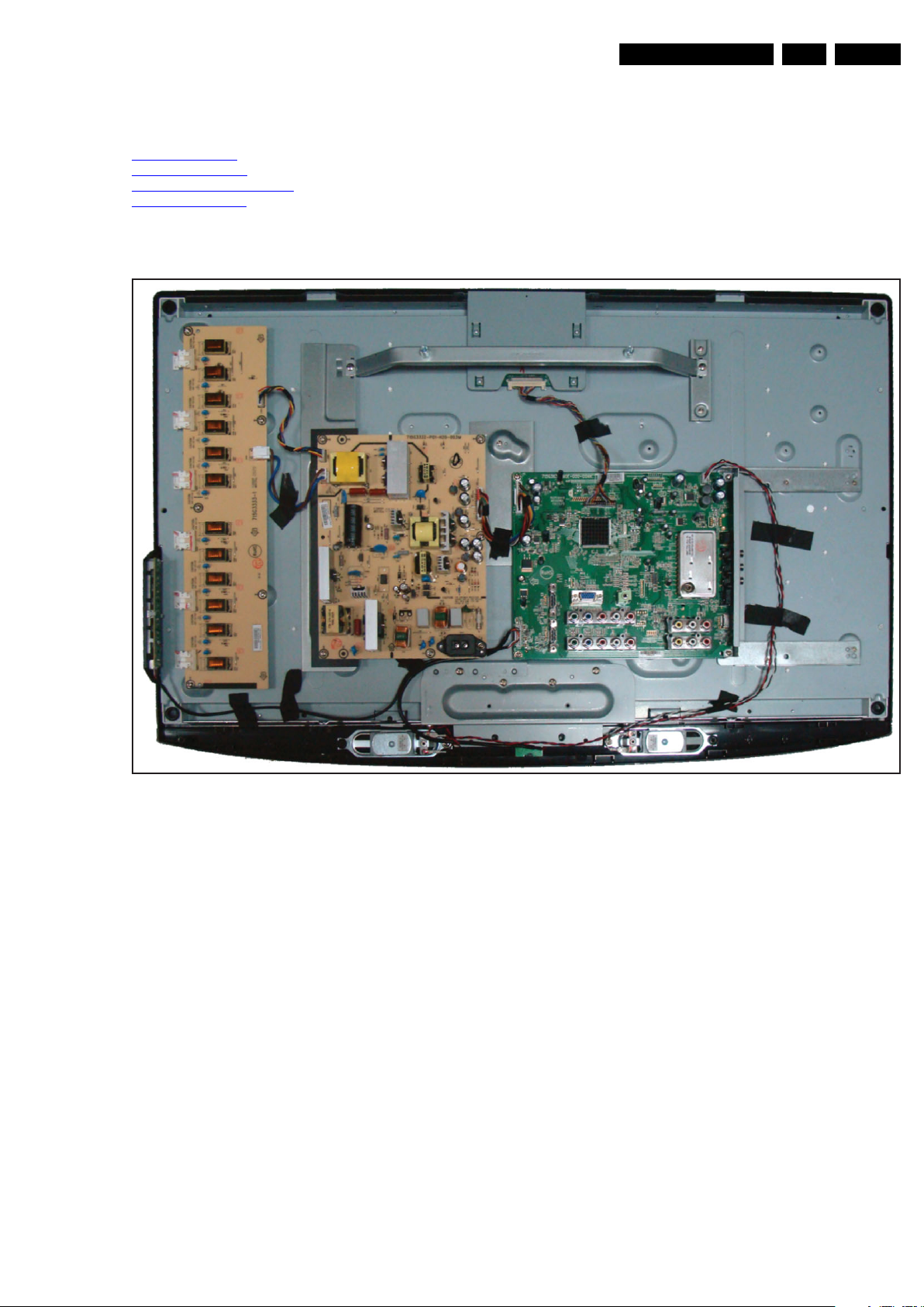
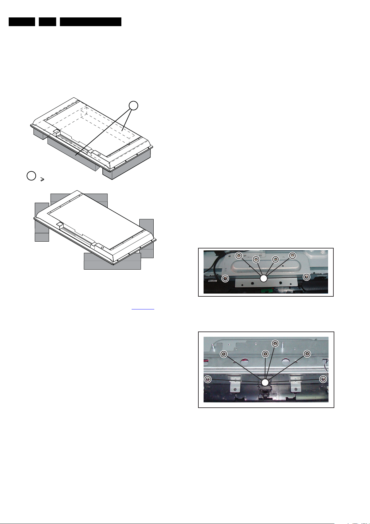
4. Mechanical Instructions
18810_100_090930.eps
091012
Mechanical Instructions
EN 9TPH1.1A LA 4.
Index of this chapter:
4.1 Cable Dressing
4.2 Service Positions
4.3 Assembly/Panel Removal
4.4 Set Re-assembly.
4.1 Cable Dressing
Notes:
• Figures below can deviate slightly from the actual situation,
due to the different set executions.
Figure 4-1 Cable dressing 32" set
2009-Dec-18
Page 10
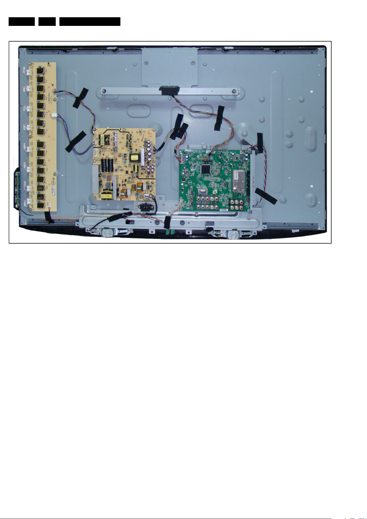
EN 10 TPH1.1A LA4.
18810_102_091009.eps
091012
Mechanical Instructions
Figure 4-2 Cable dressing 42" set
2009-Dec-18
Page 11
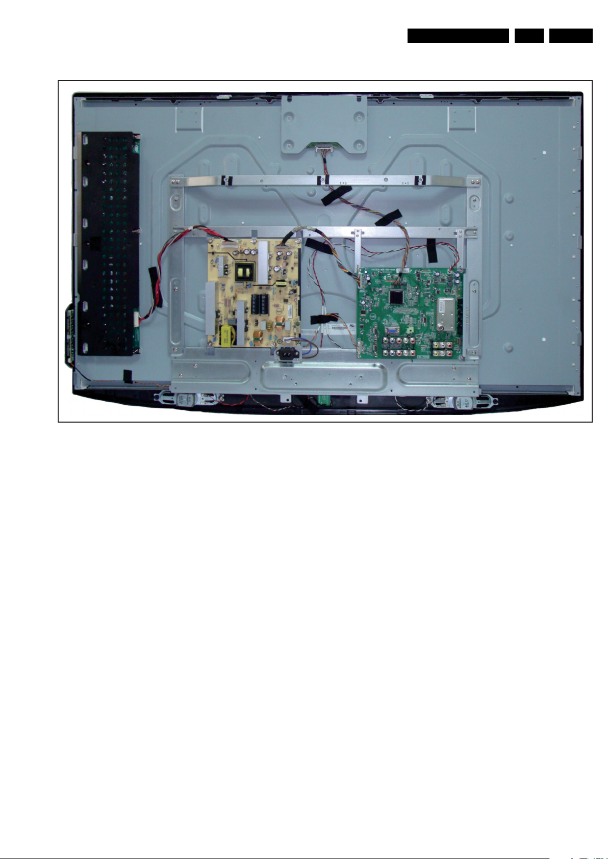
Mechanical Instructions
18811_104_091021.eps
091215
EN 11TPH1.1A LA 4.
Figure 4-3 Cable dressing 47" set
2009-Dec-18
Page 12
EN 12 TPH1.1A LA4.
18810_101_090930.eps
091215
1
18810_103_091009.eps
091012
1
Mechanical Instructions
4.2 Service Positions
For easy servicing of this set, there are a few possibilities
created:
• The buffers from the packaging.
• Foam bars (created for Service).
4.2.1 Foam Bars
Required for sets
1
42"
4.3.3 Small Signal Board (SSB)
Caution: it is mandatory to remount all different screws at their
original position during re-assembly. Failure to do so may result
in damaging the SSB.
1. Unplug LVDS connector.
Caution: be careful, as these are very fragile connectors!
2. Unplug all other connectors.
3. Remove all fixation screws.
4. The SSB can now be taken out of the set.
1
4.3.4 Power Board and Inverter Board
1. Unplug all the connectors.
2. Remove all the screws.
3. Lift the units and take them out of the set.
When defective, replace the whole unit.
Note: Inverter board is only for 32" and 42" sets.
4.3.5 Speakers
Each speaker unit is mounted with a screw.
When defective, replace the whole unit.
4.3.6 Base support
1. Remove SSB as earlier described.
2. Remove power board and inverter board as earlier
described.
3. Remove the speakers as earlier described.
4. Remove screws [1] and take the base support from the
unit.
10000_018_090121.eps
Figure 4-4 Foam bars
The foam bars (order code 3122 785 90580 for two pieces) can
be used for all types and sizes of Flat TVs. See Figure 4-4
details. Sets with a display of 42" and larger, require four foam
bars [1]. Ensure that the foam bars are always supporting the
cabinet and never only the display.
Caution: Failure to follow these guidelines can seriously
damage the display!
By laying the TV face down on the (ESD protective) foam bars,
a stable situation is created to perform measurements and
alignments. By placing a mirror under the TV, the screen can
be monitored.
4.3 Assembly/Panel Removal
4.3.1 Stand
Warning: Disconnect the mains power cord before you remove
the stand.
1. Put the set in the service position.
2. Remove all screws of the stand.
3. Lift the stand from the TV.
090121
for
Figure 4-5 Base support 32"
Figure 4-6 Base support 42"
4.3.7 IR Board
4.3.2 Rear Cover
1. Remove all screws of the rear cover.
2. Lift the rear cover from the TV. Make sure that wires and
flat foils are not damaged while lifting the rear cover from
the set.
3. In case servicing is needed in a standing position, remount
the stand.
2009-Dec-18
1. Remove the base support as earlier described.
2. Unplug the IR board connector.
3. Lift the IR board and take it out of the set.
When defective, replace the whole board.
Page 13

4.3.8 Key Board
1. Release the clip at the top and take the whole unit out.
2. Unplug the connector.
3. Remove the screws and take the key board from the unit.
When defective, replace the whole unit.
4.3.9 Display Panel
1. Remove SSB as earlier described.
2. Remove power board and inverter board (only for 32" and
42") as earlier described.
3. Remove the base support (only for 32" and 42") as earlier
described.
4. Remove the IR board and key board unit as earlier
described.
5. Remove all the fixation screws that secure the panel.
6. Remove all the screws and take all the brackets from the
panel.
When defective, replace the whole unit.
4.4 Se t Re -a ss embly
To re-assemble the whole set, execute all processes in reverse
order.
Mechanical Instructions
EN 13TPH1.1A LA 4.
Notes:
• While re-assembling, make sure that all cables are placed
and connected in their original position. See Figure 4-1
Figure 4-2
• Pay special attention not to damage the EMC foams on the
SSB shields. Ensure that EMC foams are mounted
correctly.
and Figure 4-3.
,
2009-Dec-18
Page 14
EN 14 TPH1.1A LA5.
18810_200_090930.eps
091016
Service Modes, Error Codes, and Fault Finding
5. Service Modes, Error Codes, and Fault Finding
Index of this chapter:
5.1 Service Modes
5.2 Software Upgrading
5.3 Error Codes
5.4 Fault Finding and Repair Tips
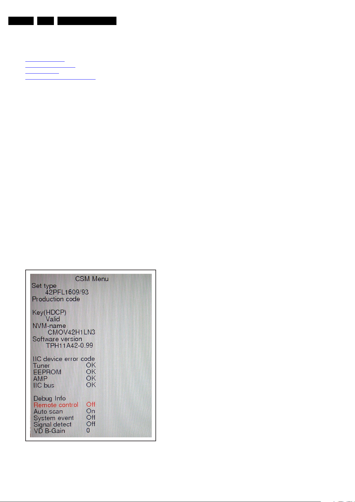
5.1 Service Modes
The Customer Service Mode (CSM) is used for communication
between the call centre and the customer, while the Factory
Mode offers several features for the service technician.
This chassis also offers the option of using ComPair, a
hardware interface between a computer and the TV chassis. It
offers the abilities of structured troubleshooting, error code
reading, and software version read-out for all chassis.
5.1.1 Customer Service Mode (CSM)
Purpose
The Customer Service Mode shows information on the TV’s
operation settings.The call centre can instruct the customer (by
telephone) to enter CSM in order to identify the status of the
set.This helps the call centre to diagnose problems and failures
in the TV set before making a service call.
The CSM is a read-only mode; therefore, modifications are not
possible in this mode.
How to Activate CSM
Key in the code “123654” via the standard RC transmitter.
Note: Activation of the CSM is only possible if there is no (user)
menu on the screen!
How to Navigate
By means of the “CURSOR-DOWN/UP” knob (or the scroll
wheel) on the RC-transmitter, can be navigated through the
menus.
Contents of CSM
• Set type. This information is very helpful for a helpdesk/
workshop as reference for further diagnosis. In this way, it
is not necessary for the customer to look at the rear of the
TV set. Note that if an NVM is replaced or is initialized after
corruption, this set type has to be re-written to NVM.
ComPair will foresee in a possibility to do this.
• Production code.
Philips serial number
• Key (HDCP).
HDCP status (Valid, Invalid)
• NVM - name.
Shows the panel type
• Software version.
Shows the software version
• I2C device error code.
The state report of I
other, normal state displaying “OK”, abnormal state
displaying “NG”.
Tuner is the tuner state.
EEPROM is the main MCU EEPROM state.
AMP is the amplifier IC state.
2
I
C bus is I2C bus state, including all I2C devices.
• Debug Info.
Shows whether print debug infomation, print debug
information sets “ON”, otherwise sets “OFF”.
How to Exit CSM
Press “MENU” on the RC-transmitter.
2
C devices communication each to
2009-Dec-18
Figure 5-1 CSM Menu
Page 15
Service Modes, Error Codes, and Fault Finding
18810_201_090930.eps
091215
EN 15TPH1.1A LA 5.
5.1.2 Factory mode
How to enter
To enter the factory mode, use the following method:
• Press “MENU” button, and then press the following key
sequence on the remote control transmitter: “062596”
directly followed by the “INFO” button.
Caution: these functions are available for development and
service personal only, not for end customers.
After entering the factory mode, the following screen is visible
on the top and right of the panel.
• SSC Enable
Turning “On” of “Off” SSC.
• SSC Step
Sets the SSC steps.
• SSC Top
Sets the SSC range.
• ADC Gain.
Sets the ADC gain R, G, B values.
• ADC Offset
Sets the ADC offset R, G, B values.
• Color temp
Sets the current colour temperature. There are three colour
temperature values: Cool, Normal, Warm.
• Scaler Gain
Sets the scaler gain R, G, B values.
• Burn in
Turns “On” or “Off” the burn in mode. When burn in is “On”,
the RC function is enabled.
• EEPROM Init
Initializes all EEPROM data except the HDCP key.
• Back LIT time
Shows the total “On” time of the backlight.
• Total time
Shows the total “On” time of the power.
• Black light
Shows the brightness of back light.
• Menu Language
Shows the menu language of user mode.
• Reset
Resets EEPROM data.
• Exit
Exit the factory mode.
Figure 5-2 Factory Mode Menu
How to Navigate
With the up/dowm cursor keys can be navigated arround the
items, with the Left/Right cursor the values can be changed.
Contents of factory mode
• Brand
Shows the Philips brand name.
• Ver
Shows the software version.
• Date
Shows the software issue date.
• Model name
Shows the model number.
• Scaler
Shows the scaler type.
• Panel type
Shows the panel type.
• Current source
Shows the current source name. The input source can be
changed with the Left/Right cursor keys.
• Auto White 100%
Adjusts ADC in PC and YPbPr mode.
• Auto White 75%
Adjusts ADC in PC and YPbPr mode.
• SSC (Spread Spectrum Clocking) Channel
Shows the place of SSC. “Pllm” sets memory SSC, “Pllo”
sets LVDS SSC.
How to EXIT
Choose “Exit”, then press “OK” button.
5.2 Software Upgrading
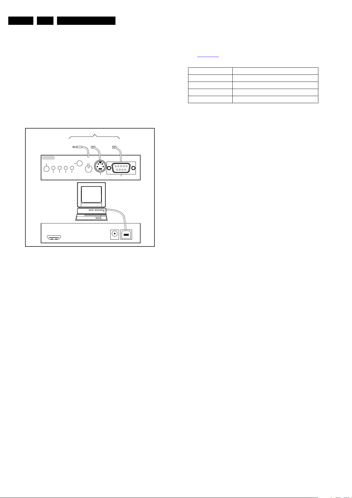
5.2.1 ComPair
Introduction
ComPair (Computer Aided Repair) is a Service tool for Philips
Consumer Electronics products. and offers the following:
1. ComPair helps to quickly get an understanding on how to
repair the chassis in a short and effective way.
2. ComPair allows very detailed diagnostics and is therefore
capable of accurately indicating problem areas. No
knowledge on I
because ComPair takes care of this.
3. ComPair speeds up the repair time since it can
automatically communicate with the chassis (when the uP
is working) and all repair information is directly available.
4. ComPair features TV software up possibilities.
2
C or UART commands is necessary,
2009-Dec-18
Page 16
EN 16 TPH1.1A LA5.
Service Modes, Error Codes, and Fault Finding
Specifications
ComPair consists of a Windows based fault finding program
and an interface box between PC and the (defective) product.
The ComPair II interface box is connected to the PC via an
USB cable. For the TV chassis, the ComPair interface box and
the TV communicate via a bi-directional cable via the service
connector(s).
The ComPair fault finding program is able to determine the
problem of the defective television, by a combination of
automatic diagnostics and an interactive question/answer
procedure.
How to Connect
This is described in the chassis fault finding database in
ComPair.
TO TV
TO
TO
UART SERVICE
CONNECTOR
2
I
C
RS232 /UART
ComPair II
RC in
Optional
Switch
Power ModeLink/
Activity
UART SERVICE
CONNECTOR
RC out
TO
I2C SERVICE
CONNECTOR
Multi
function
PC
5.3 Error Codes
The error codes can be read out via the CSM menu,
see Figure 5-1
.
Error Codes Event
Tuner Tuner state
EEPROM Main MCU EEPROM state
AMP Amplifier IC state
2
C bus I2C bus state
I
5.4 Fault Finding and Repair Tips
5.4.1 Exit “Factory mode”
Choose “EXIT”, then press “OK” button. Turn “Off” the TV and
then turn “On” the TV.
5.4.2 Speakers
Make sure that the volume is set to minimum during
disconnecting the speakers in the ON-state of the TV. The
audio amplifier can be damaged by disconnecting the speakers
during ON-state of the set!
ComPair II Developed by Philips Brugge
Optional power
HDMI
2
I
C only
5V DC
10000_036_090121.eps
091118
Figure 5-3 ComPair II interface connection
Caution: It is compulsory to connect the TV to the PC as
shown in the picture above (with the ComPair interface in
between), as the ComPair interface acts as a level shifter. If
one connects the TV directly to the PC (via UART), ICs will be
blown!
How to Order
ComPair II order codes:
• ComPair II interface: 3122 785 91020.
• Programming software can be downloaded from the Philips
Service portal.
2
•I
C adapter cable for TPH1.1x xx.
9965 100 09269.
Note: When having problems, contact the local support desk.
2009-Dec-18
Page 17
6. Alignments
Alignments
EN 17TPH1.1A LA 6.
Index of this chapter:
6.1 General Alignment Conditions
6.2 Hardware Alignments
6.3 Software Alignments
6.4 Serial Number Definition
6.5 Display option codes
Note: The Service Mode are described in chapter 5. Menu
navigation is done with the CURSOR UP, DOWN, LEFT or
RIGHT keys of the remote control transmitter.
6.1 Gen e r al Ali gn me n t Co nd it io n s
Perform all electrical adjustments under the following
conditions:
• Power supply voltage (depends on region):
– 100 V to 240 V
• Connect the set to the mains via an isolation transformer
with low internal resistance.
• Allow the set to warm up for approximately 15 minutes.
• Measure voltages and waveforms in relation to correct
ground (e.g. measure audio signals in relation to
AUDIO_GND).
Caution: It is not allowed to use heatsinks as ground.
• Test probe: R
• Use an isolated trimmer/screwdriver to perform
alignments.
, 50/60 ±3 Hz.
AC
> 10 MΩ, Ci < 20 pF.
i
6.2 Hardware Alignments
Not applicable.
6.3 Software Alignments
• Set the RED, GREEN and BLUE default values according
to the values in the “Tint settings” table.
• After finished, exit the factory menu and restart the TV set.
Table 6-2 Tint settings
Colour Temp R G B
Warm 128 128 128
Normal 128 128 128
Cool 128 128 128
6.4 Serial Number Definition
BOM Code:
Table 6-3 BOM Code
Panel Supplier Code
AU 1
CPT 2
LPL(LG) 3
QDI 4
CMO 5
HSD 6
SVA 7
6.5 Display option codes
This chassis does not have display options codes.
• Choose “MENU”, “Picture” and set “Picture mode” as
“Standard”.
• Put the set in factory mode (see Chapter 5. Service Modes,
Error Codes, and Fault Finding.). The factory menu will
now appear on the screen.
If you do not have a colour analyser:
• Measure with a calibrated contactless colour analyser in
the centre of the screen. Consequently, the measurement
needs to be done in a dark environment. To adjust the
scaler gain with direction key and menu key.
• Adjust the correct x, y coordinated (while holding one of the
white point registers R, G or B on 128) by means of
decreasing the value of one or two other white points to the
correct x, y coordinates.
• Repeat this step for the other colour temperatures that
need to be aligned.
• When finished, then exit the factory menu and restart the
TV.
Table 6-1 White alignment values
Colour
Temp
x 290 ± 0.015 280 ± 0.015 260 ± 0.015
y 295 ± 0.015 285 ± 0.015 266 ± 0.015
Y 350 ± 0.015 350 ± 0.015 350 ± 0.015
Warm
(8000K)
Normal
(10000K)
Cool
(13000K)
If you do not have a colour analyser, you can use the default
values. This is the next best solution. The default values are
average values coming from production (statistics).
• Select NORMAL COLOUR TEMPERATURE (e.g. Cool,
Normal, Warm).s
2009-Dec-18
Page 18
EN 18 TPH1.1A LA7.
18811_203_091023.eps
091215
HX6202A
8
FLASH
M15WPP-2PN-E
Hybrid Tuner
R2A15112FP
Audio AMP
74HC4052D
Audio Switch
Video &
audio
decoder
AV × 2
YPbPr × 2
HDMI × 3
S-video ×1
VGA
APA2176A
AV OUT
PANEL
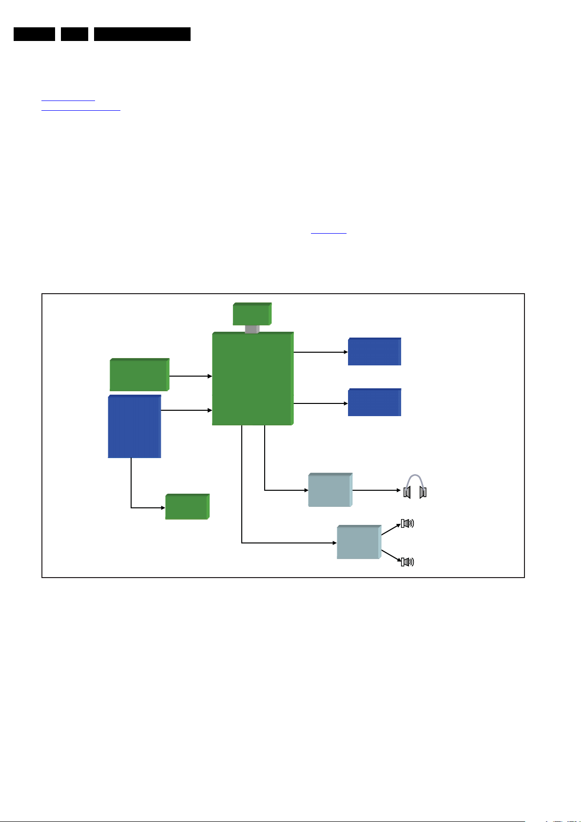
7. Circuit Descriptions
Circuit Descriptions
Index of this chapter:
7.1 Introduction
7.2 Power Architecture
Notes:
•Only new circuits (circuits that are not published recently)
are described.
• Figures can deviate slightly from the actual situation, due
to different set executions.
• For a good understanding of the following circuit
descriptions, please use the wiring, block (see chapter
9. Block Diagrams) and circuit diagrams (see chapter
10. Circuit Diagrams and PWB Layouts). Where
necessary, you will find a separate drawing for clarification.
7.1 Introduction
The chassis uses the same scaler board but that is the
separation of the power supply unit.
7.1.1 Implementation
Key components of this chassis:
• HX6202 - A09 video and audio decoder
• HX6202 - A09 video and audio decoder
• HX6202 - A09 video and audio decoder
• M15WPP - 2PN - Bird tuner
• 74HC4052D audio switch
• R2A15112FP audio amplifier
7.1.2 TV Architecture Overview
For details about the chassis block diagrams refer to 9. Block
Diagrams. An overview of the TV architecture can be found in
Figure 7-1
2009-Dec-18
Figure 7-1 TV Architecture Overview
Page 19
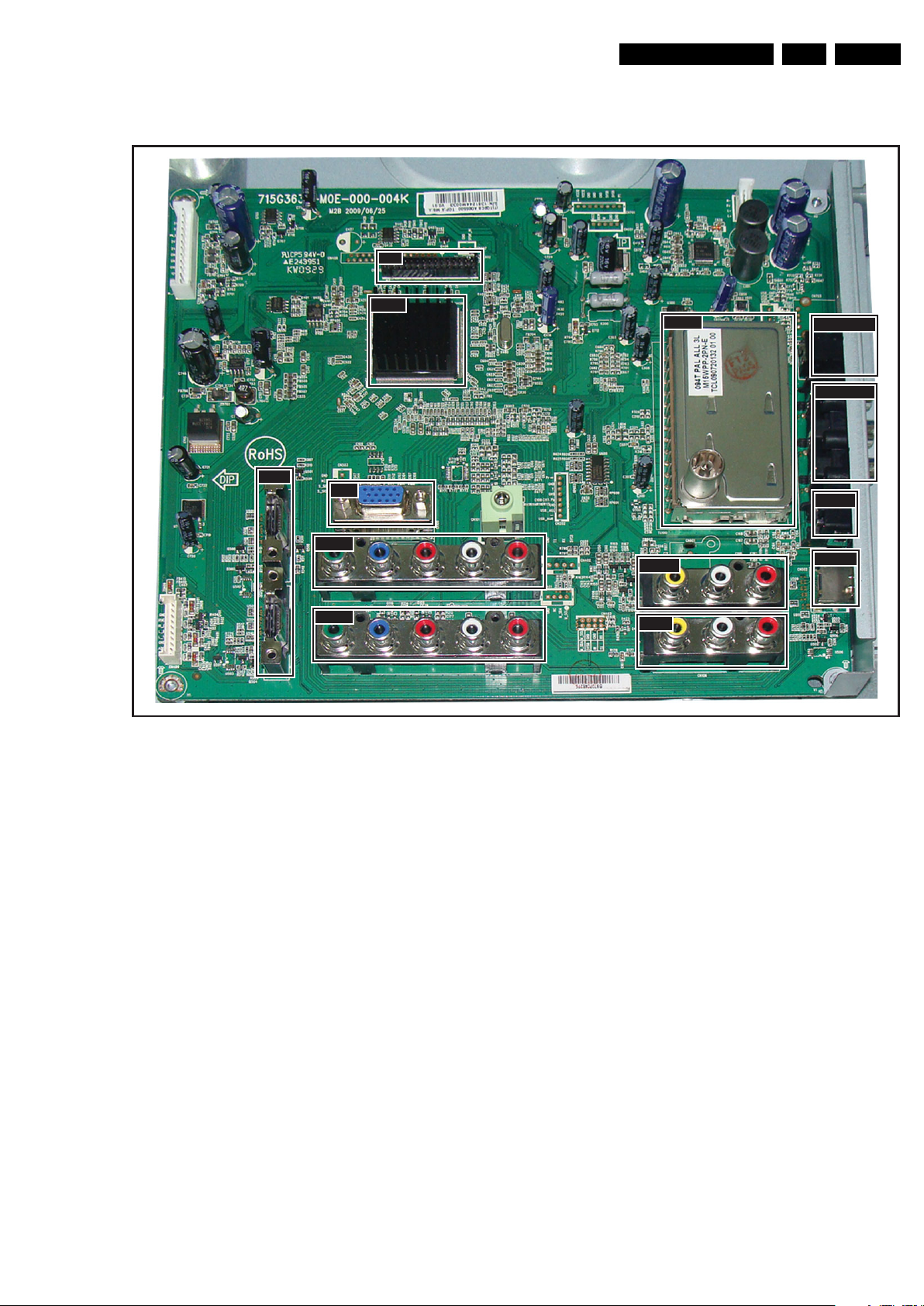
7.1.3 SSB Cell Layout
18810_206_090927.eps
090927
TUNER
FFC
Scaler
HDMI
VGA
AV OUT
AV IN
HeadPhone
S-Video
AV IN
HDMI
EXT1
EXT2
Circuit Descriptions
EN 19TPH1.1A LA 7.
Figure 7-2 SSB Cell layout
2009-Dec-18
Page 20
EN 20 TPH1.1A LA7.
1084-33
U705
+5V_SB
5VSB
VCC3
VCCK18
SC4524B
U707
AO4449
Q705
VCC5
POWER_ON
AP1117D33
U703
V33_AUD
V33_HDMI_ADC
V33ADC_PLL / AVDD_ADC
VCC3IO / V33LV
HX6202A
U400
VCC3
MX25L4005AM2C
U402
V33HDMI / VCCADC / VDDA33
HX6202A
U400
V33AUD
HX6202A
U400
VCC5
5VSB
5VSB
V33_AUD
VCCK
V33ADC_PLL / AVDD_ADC
VCC3IO / V33LV
HX6202A
U400
V33HDMI / VCCADC / VDDA33
V33AUD
AVDD18 / VDDD18 / V18AUD
94mA
1.5A
92mA
981mA
121mA
AP1117D33
U702
AP1117D18
U700
AVDD18 / VDDD18
V18AUD
HX6202A
U400
VCCK
HX6202A
U400
VCC18
AP2176
U601
EARPHONE AMP
PI5V33
U107
VIDEO SWITCH
USB boad power
5V,5V TO 3.3v
5v to 1.8V
VCC5
VCC5VCC5
5VSB
M24C02
U502
M24C02
U506
M24C02U503
M24C02
U100
M24C32
U401
5VSB5VSB5VSB5VSB
VCC5
5VSB
400mA
V12_ADP
+12V_SB
POWER_ON
AO3407
Q701
74HC4052
U600
AUDIO SWITCH
VCC12
BA17808
ZD700
A1117D5.0
U300
VCC8
+24V
+5VT
TUNER
TU100
R2A15112FP
V24_ADP
PANEL_VCC
AO4449
Q405
PANEL
PANEL
PANEL_VCCAO4449
Q405
V12_ADP
PANEL_ON
PANEL_ON
5VSB
USB HOST
MPS2171
U711
POWER_ON
8mA
160mA
500mA--1.0A
U603
18810_402_090925.eps
091215
7.2 Power Architecture
Circuit Descriptions
2009-Dec-18
Figure 7-3 Power Architecture
Page 21
7.2.1 Power Supply Unit
All power supplies are a black box for Service. When defective,
a new board must be ordered and the defective one must be
returned, unless the main fuse of the board is broken. Always
replace a defective fuse with one with the correct
specifications! This part is available in the regular market.
Consult the Service website for the order codes of the boards.
In this manual, no detailed information is available because of
design protection issues.
The output voltages to the chassis are:
• +1V8-STANDBY
• +3V3-STANDBY
• +5V (BL_ON, BL_ADJ, PANEL_ON)
• +12V (PW_ON)
• +24V (PW_ON)
• IPB: High voltage to the LCD panel.
7.2.2 Diversity
Below find an overview of the different PSUs that are used:
Table 7-1 Supply diversity
Circuit Descriptions
EN 21TPH1.1A LA 7.
PSU Model Input Voltage Range
715G 3332 P01H 2000 3M
715G 3351 1 HV 42" High Mains (100- 240 Vac)
715G 3196 1 HV 47" High Mains (100- 240 Vac)
32" High Mains (100- 240 Vac)
2009-Dec-18
Page 22
EN 22 TPH1.1A LA8.
YPbPr
ADC
ADC PLLHs/Vs
Video Pre-
Processing
GE
OSD
Mixer
Reg
PLL/SSC
Panel
Ext. Clock
HDMI1
LV
DS
TX
RGB
Input Mux
MU
X
R
SDS
T
X
T
C
O
N/
B
a
c
k
en
d
DTV YPbPr
Video
Decoder
IR
INTR
PWMs/
GPIOs
HDMI 1.3
3D Video
Processing
MCU
Audio Demod/Processor
Audio DACs
L/R ADCs
SIF ADC
L/R1
L/R2
L/R3
L/R4
SIF P/N
HDMI2
HDMI3
SCART
CVBS/SV
Tuner
Audio Amp for
loud speaker
Audio Amp for
ear phone
SCART Audio Out
S/PDIF TX
S/PDIFO
S/PDIF RX
DTV S/PDIFO
Video PostProcessing
LB ADC
IR TxK e y Pad
DRAM
SPI
Flash
LIPS
18810_300_090928.eps
091216
Block Diagram
Pin Configuration
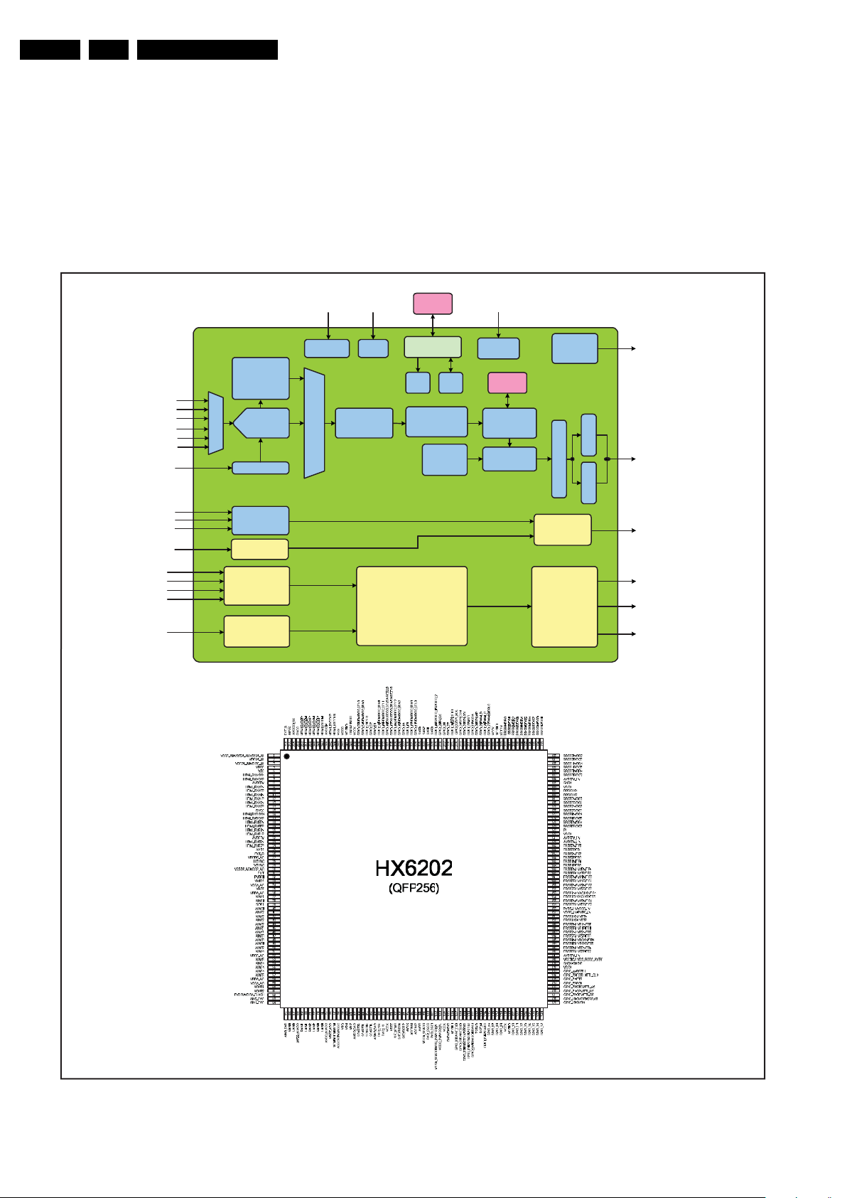
8. IC Data Sheets
This section shows the internal block diagrams and pin
configurations of ICs that are drawn as “black boxes” in the
electrical diagrams (with the exception of “memory” and “logic”
ICs).
8.1 HX6202 (IC U400)
IC Data Sheets
2009-Dec-18
Figure 8-1 Internal block diagram and pin configuration
Page 23
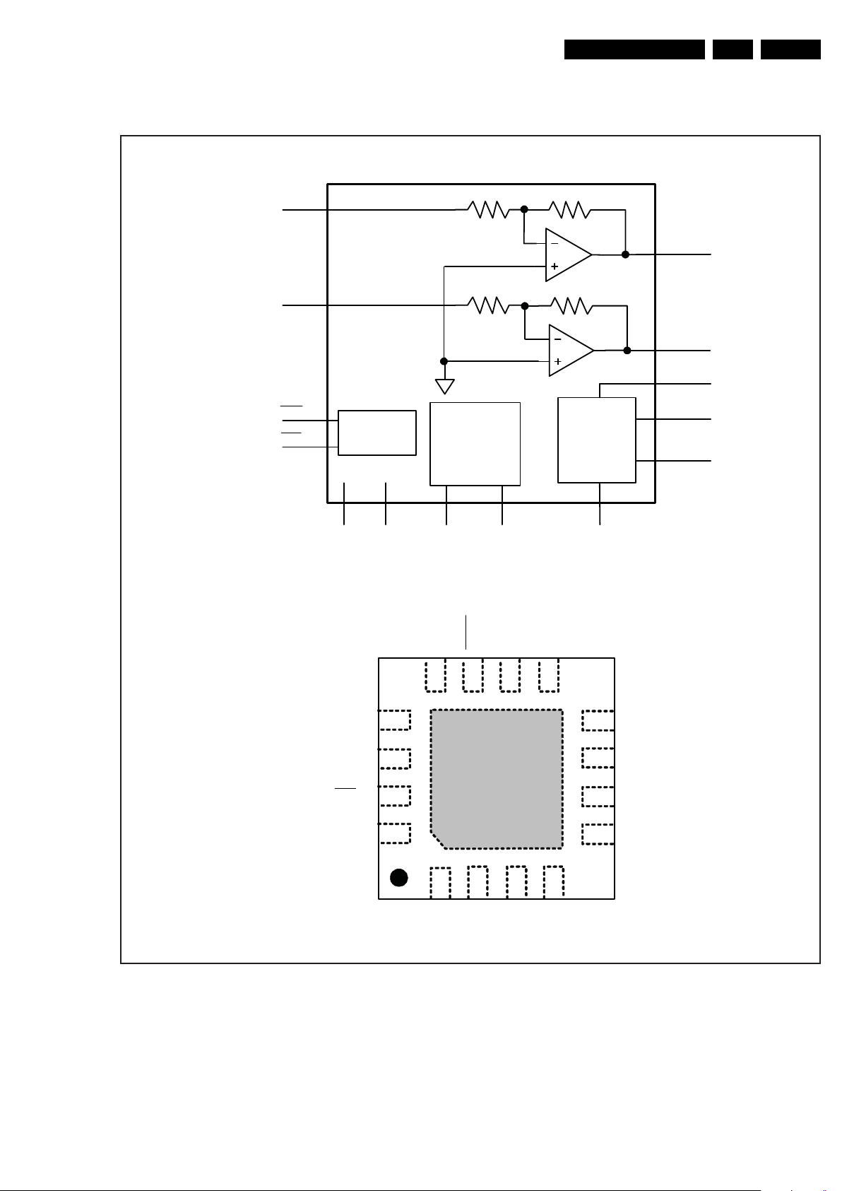
8.2 APA2176A (IC U601)
18810_302_090928.eps
091216
APA2176A
5 CVSS
6 VSS
7 LOUT
8 V
DD
CP + 1
PGND 2
CP - 3
NC 4
9 ROUT
10 LIN
11 RSD
12 RIN
NC 13
GND 14
LSD 15
PVDD 16
Shutdown
circuit
Power and
Depop circuit
ROUT
RIN
RSD
Charge
Pump
circuit
LIN
LOUT
GND
VDD
CP+
CP-
CVSSVSSPGND
PVDD
LSD
GND
Block Diagram
Pin Configuration
IC Data Sheets
EN 23TPH1.1A LA 8.
Figure 8-2 Internal block diagram and pin configuration
2009-Dec-18
Page 24
EN 24 TPH1.1A LA8.
27
29 28303233 3134
39
43
41
42
40
45
44
46
37
38
47
48
8
6 7
5
32 41
12
10 119
22
18
20
19
21
16
17
15
24
23
14
13
3536 26 25
N.C.
OUT2
N.C.
N.C.
GAIN2
VD2
VD2
N.C.
IN2
OUT2
MUTEL
N.C.
N.C
HB2
HB1
N.C.
N.C.
DVDD
VS2
VS2
N.C.
VS1
N.C.
VS1
GAIN1
N.C.
OUT1
N.C.
VD1
N.C.
IN1
VD1
N.C.
N.C.
OUT1
STBYL
N.C.
N.C.
N.C.
N.C.
GND
AVCC
CLOCK
PROT
ROSC
N.C.
VREF
CBIAS
R2A15112FP
Under Voltage
Detection
Over Temp.
Detection
Over Current
Detection
Control
Logic
STBYL
GND
IN1
A
MUTEL
PROT
CBIAS
A
IN2
PWM
Gen.
PWM
Gen.
Oscillator
ROSC
GAIN1 GAIN2
SE/BTL
Selector
OUT1
HB1
VD1
VS1
OUT2
VD2
VS2
HB2
DVDD
AVCC
R
L
CLOCK
VREF
10V
5V
18810_303_090928.eps
091216
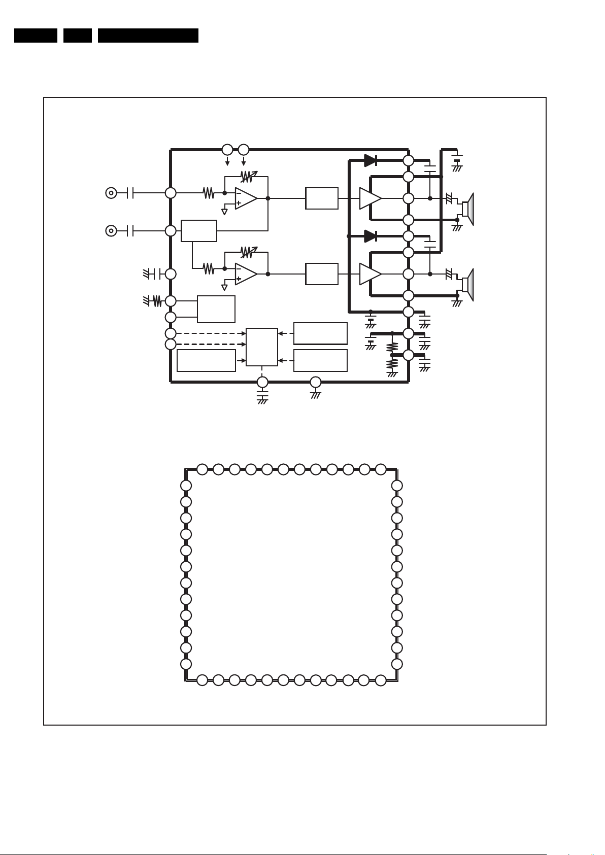
Block Diagram
Pin Configuration
8.3 R2A15112FP (IC U603)
IC Data Sheets
2009-Dec-18
Figure 8-3 Internal block diagram and pin configuration
Page 25

8.4 AZ1117D (IC U300, U700)
INPUT
OUTPUT
ADJ/GND
V
OUT
1
2
3
Thermal
Protection
+
-
For Adjustable Output, disconnect A1 and A2, connect B
INPUT
OUTPUT
ADJ/GND
A1
A2
B
For Fixed Output, connect A1 and A2, disconnect B
18810_304_090928.eps
091216
Block Diagram
Pin Configuration
IC Data Sheets
EN 25TPH1.1A LA 8.
Figure 8-4 Internal block diagram and pin configuration
2009-Dec-18
Page 26

EN 26 TPH1.1A LA8.
3
Thermal
Shutdown
1
2
V
OUT
Adj
1.25V
+
+
CURRENT
LIMIT
V
IN
-
+
+
1
GND
(FIXED)
-
3
2
1
VIN
VOUT
Adj (GND)
18810_305_090928.eps
091216
Block Diagram
Pin Configuration
8.5 AP1117D (IC U702, U703)
IC Data Sheets
Figure 8-5 Internal block diagram and pin configuration
2009-Dec-18
Page 27

8.6 SC4524BSETRT (IC U707)
1
2
3
4
BSTSW
7
6
8
5
FBIN
COMPROSC
SS/ENGND
9
IN
2
ROSC
3
TRANSISTORR
Q
S
POWER
SLOPE
COMP +
-
ISEN
ILIM
+
-
20mV
6.1m ohm
+
+
S
BST
REFERENCE
& THERMAL
SHUTDOWN
1V
FAULT
OVERLOAD
SOFT
AND
OVERLOAD
HICCUP
CONTROL
1.9V
R
8
SW
1
FB
7
SS/EN
5
COMP
6
OSCILLATOR
CLK
EA
PWM
+
-
+
1.23V
-
FREQUENCY
FOLDBACK
GND
4
+
+
-
R
OC
PWM
A1
V1
3
+
-
+
BST
START
7
5
6
+
-
+
-
+
+
-
18810_306_090929.eps
091216
Block Diagram
Pin Configuration
IC Data Sheets
EN 27TPH1.1A LA 8.
Figure 8-6 Block diagram and pin configuration
2009-Dec-18
Page 28

EN 28 TPH1.1A LA8.
Personal Notes:
10000_012_090121.eps
090121
IC Data Sheets
2009-Dec-18
Page 29

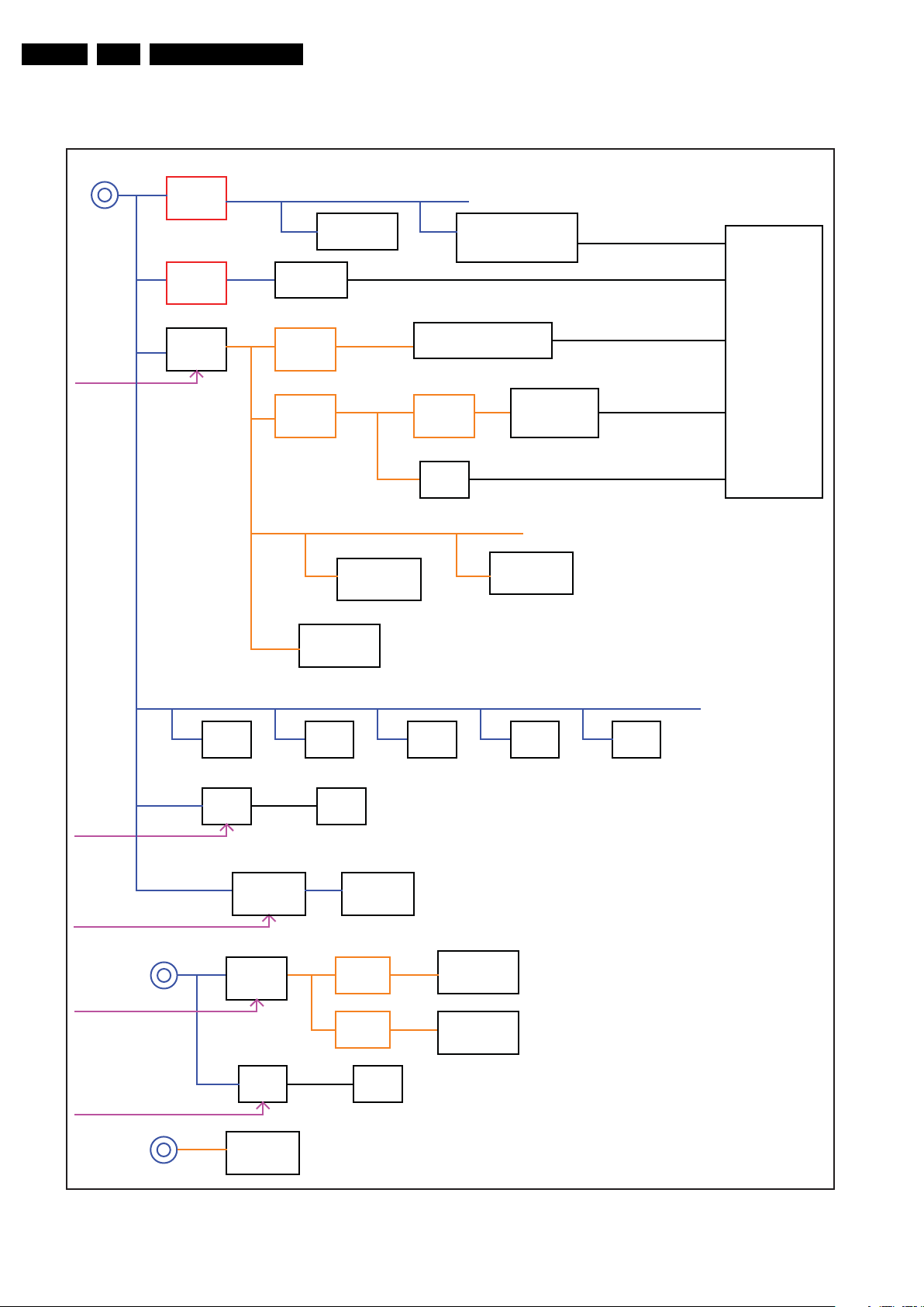
9. Block Diagrams
IR BOARD
(FQ007)
Board Level Repair
Component Level Repair
Only For Authorized Workshop
KEYBOARD CONTROL
(FQ004)
CN01
4P
RIGHT SPEAKER
POWER SUPPLY IPB
FQ009
MAIN POWER SUPPLY PSU
FQ003
LEFT SPEAKER
+
-
-
+
LCD DISPLAY (FQ001)
CN8808
2P
CN8807
2P
CN8806
2P
CN8805
2P
CN8804
2P
CN8803
2P
CN8801
6. VS
5. IS1
4. GND
3. IS2
2. N.C.
1. GND
CN8802
1. TB
2. TA
CN802
5. VS
4. IS1
3. GND
2. IS2
1. GND
CN801
2. TB
1. TA
CN902
1. ON/OFF
2. PDIM
3. +12V
4. +12V
5. GND
6. GND
7. GND
8. +24V
9. +24V
10. PS_ON
11. +5V
12. +5V
CN700 (B01)
12. +5VSB
11. +5VSB
10. PWR_ON
9. +24V
8. +24V
7. GNDP
6. GNDP
5. GNDP
4. +12V
3. +12V
2. BL_ADJ
1. BL_ON
CN400 (B08)
10. L_SEN
9. GND
8. IRVCC
7. IR_D
6. L_B
5. L_Y
4. GND
3. ADC
2. PW
1. N.C.
SSB
(FQ002)
B
A
A
J
CN405 (B09)
29. TX0AP
27. TX1AP
25. TX2AP
...
...
...
5. VCC5_IN
3. GND
1. GND
30. TX0AN
28. TX1AN
26. TX2AN
...
...
...
6. VCC5_IN
4. SELLVDS
2. GND
CN602(B07)
1. R-
2. R+
3. L-
4. L+
CN01
5P
TO
BACKLIGHT
18810_400_090925.eps
091016
TO
BACKLIGHT
TO
BACKLIGHT
TO
BACKLIGHT
TO
BACKLIGHT
TO
BACKLIGHT
Wiring Diagram 32"
Block Diagrams
EN 29TPH1.1A LA 9.
2009-Dec-18
Page 30

IR BOARD
(FQ007)
Board Level Repair
Component Level Repair
Only For Authorized Workshop
KEYBOARD CONTROL
(FQ004)
CN01
4P
RIGHT SPEAKER
POWER SUPPLY IPB
FQ009
MAIN POWER SUPPLY PSU
FQ003
LEFT SPEAKER
+
-
-
+
CN901
N
L
LCD DISPLAY
(FQ001)
CN8810
2P
CN8801
1. GND
2. N.C.
3. IS2
4. GND
5. IS1
6. VS
CN8802
1. TB
2. TA
CN802
5. VS
4. IS1
3. GND
2. IS2
1. GND
CN801
2. TB
1. TA
CN400
(B08)
10. L_SEN
9. GND
8. IRVCC
7. IR_D
6. L_B
5. L_Y
4. GND
3. ADC
2. PW
1. N.C.
SSB
(FQ002)
B
A
A
J
CN602
(B07)
1. R-
2. R+
3. L-
4. L+
CN01
5P
TO
BACKLIGHT
CN8809
2P
TO
BACKLIGHT
CN8808
2P
TO
BACKLIGHT
CN8807
2P
TO
BACKLIGHT
CN8806
2P
TO
BACKLIGHT
CN8805
2P
TO
BACKLIGHT
CN8804
2P
TO
BACKLIGHT
CN8803
2P
TO
BACKLIGHT
18810_403_091009.eps
091016
CN902
1. ON/OFF
2. PDIM
3. +12V
4. +12V
5. GND
6. GND
7. GND
8. +24V
9. +24V
10. PS_ON
11. +5V
12. +5V
CN700
(B01)
12. +5VSB
11. +5VSB
10. PWR_ON
9. +24V
8. +24V
7. GNDP
6. GNDP
5. GNDP
4. +12V
3. +12V
2. BL_ADJ
1. BL_ON
CN405
(B09)
29. TX0AP
27. TX1AP
25. TX2AP
...
...
...
5. VCC5_IN
3. GND
1. GND
30. TX0AN
28. TX1AN
26. TX2AN
...
...
...
6. VCC5_IN
4. SELLVDS
2. GND
Wiring Diagram 42"
Block Diagrams
EN 30TPH1.1A LA 9.
2009-Dec-18
Page 31

Wiring Diagram 47"
IR BOARD
(FQ007)
Board Level Repair
Component Level Repair
Only For Authorized Workshop
KEYBOARD CONTROL
(FQ004)
CN01
4P
RIGHT SPEAKER
MAIN POWER SUPPLY PSU
FQ003
LEFT SPEAKER
+
-
-
+
CN901
N
L
LCD DISPLAY
(FQ001)
CN400
(B08)
10. L_SEN
9. GND
8. IRVCC
7. IR_D
6. L_B
5. L_Y
4. GND
3. ADC
2. PW
1. N.C.
SSB
(FQ002)
B
A
J
CN602
(B07)
1. R-
2. R+
3. L-
4. L+
CN01
5P
18811_404_091021.eps
091215
CN903
1. 24V
2. 24V
3. 24V
4. 24V
5. 24V
6. GND
7. GND
8. GND
9. GND
10. GND
11. ENABLE
12. ON / OFF
13. DIM
CN904
(Optional)
1. 24V
2. 24V
3. 24V
4. 24V
5. 24V
6. GND
7. GND
8. GND
9. GND
10. GND
11. ENABLE
12. ON / OFF
13. DIM
CN905
1. ON / OFF
2. DIM
3. 12V
4. 12V
5. GND
6. GND
7. GND
8. 24V
9. 24V
10. PS_ON
11. 5V
12. 5V
CN700
(B01)
12. +5VSB
11. +5VSB
10. PWR_ON
9. +24V
8. +24V
7. GNDP
6. GNDP
5. GNDP
4. +12V
3. +12V
2. BL_ADJ
1. BL_ON
CN405
(B09)
29. TX0AP
27. TX1AP
25. TX2AP
...
...
...
5. VCC5_IN
3. GND
1. GND
30. TX0AN
28. TX1AN
26. TX2AN
...
...
...
6. VCC5_IN
4. SELLVDS
2. GND
LCD DISPLAY
(FQ001)
Block Diagrams
EN 31TPH1.1A LA 9.
2009-Dec-18
Page 32

Block Diagram Audio and Video
HDMI A
HDMI B
Analog Audio
Analog Audio
Analog Vi deo
Analog Video
Analog Vi deo
HDMI C
CVBS
HDMI B
HDMI A
YPbPr /AUDIO 1
VGA-AUDIO
VGA
SWITCH
74HC4052
TUNER
AUDIO
YPbPr /AUDIO 2
AUDIO MONO
AUDIO
Audio IF
HDMI EDID C
HDMI EDID B
HDMI EDID A
VGA EDID
SDA/SCL
SDA/SCL
SDA/S CL
SDA/SCL
RX/TX
AUDIO1
CVBS1+S-VIDEO
S -VIDEO_Y
AV1_CVBS
AV_OUT
AV1_AUD IO
S -VIDEO_C
AV2_CVBS
CVBS2+AUDIO2
CVBS_OUT
AV2_AUD IO
AUDIO_OUT
FLASH
EPROM
SCL/SDA_A
SCL/SDA_A
SCL/SDA_A
AOC HOTEL
RX/TX
RX/TX
HDMI C
R2A15112FP
S PEAKER
SPDIF
APA2176A
HEADPHONE
LVDS con nector
OUTPUT
Other
IR/LED
Keypad
VCO 24.576MHz
LVD S
RA IN0/LAIN0
S IF +/-
AIN 3 7,38,39,40
B, G, R, S OG
HDMI A
AIN 41,42,43,44
S OY, Y, Pb , Pr
AIN50: CV_Y
DAC_LS R/L
AIN56: CVBS _2
AIN 45,46,47,48
S OY, Y, Pb , Pr
HDMI C
HDMI B
S PD IF
S CART2R/L
RAIN2/LAIN2
RAIN3/LAIN3
SCART1 R/L
AIN49: CVBS _1
M2B
AOUT2:CVBS _O
RAIN1/LAIN1
AIN51: CV_C
AIN57: T_CVBS
HX6202-A
18810_401_090925.eps
091013
Block Diagrams
EN 32TPH1.1A LA 9.
2009-Dec-18
Page 33

Block Diagram Power Diagram
Personal Notes:
10000_012_090121.eps
090121
Block Diagrams
EN 33TPH1.1A LA 9.
+5V_SB
POWER_ON
981mA
5VSB
5VSB
5VSB
1084-33
U705
SC4524B
U707
AO4449
Q705
92mA
1.5A
VCCK18
VCC5
VCC5
400mA
VCC5
VCC3
VCC3
MX25L4005AM2C
U402
VCCK
HX6202A
U400
AP1117D33
U702
AP1117D33
U703
VCC5
USB boad power
5V,5V TO 3.3v
5v to 1.8V
94mA
V33_HDMI_ADC
121mA
V33_AUD
V33_AUD
PI5V33
U107
VIDEO SWITCH
V33ADC_PLL / AVDD_ADC
VCC3IO / V33LV
HX6202A
U400
V33HDMI / VCCADC / VDDA33
HX6202A
U400
AVDD18 / VDDD18
VCC18
AP1117D18
U700
V33AUD
HX6202A
U400
VCC5VCC5
V18AUD
HX6202A
U400
AP2176
U601
EARPHONE AMP
V33ADC_PLL / AVDD_ADC
VCC3IO / V33LV
VCCK
V33HDMI / VCCADC / VDDA33
HX6202A
U400
AVDD18 / VDDD18 / V18AUD
V33AUD
PANEL_ON
POWER_ON
POWER_ON
PANEL_ON
5VSB
500mA--1.0A
+12V_SB
+24V
5VSB
V12_ADP
V24_ADP
M24C02
U502
AO4449
Q405
V12_ADP
PANEL_VCC
MPS2171
U711
AO3407
Q701
Q405
R2A15112FP
U603
VCC12
PANEL_VCCAO4449
M24C02U503
PANEL
USB HOST
BA17808
ZD700
A1117D5.0
U300
PANEL
8mA
VCC8
160mA
+5VT
M24C02
U506
5VSB5VSB5VSB5VSB
74HC4052
U600
AUDIO SWITCH
TUNER
TU100
M24C02
U100
5VSB
M24C32
U401
18810_402_090925.eps
091215
2009-Dec-18
Page 34

Circuit Diagrams and PWB Layouts
10. Circuit Diagrams and PWB Layouts
EN 34TPH1.1A LA 10.
Power Board Power, 32"
!
2
2
1
!
C902
C902
680pF
680pF
!
!
R901
R901
SG901NCSG901
NC
12
NR901
NR901
NTCR
NTCR
t
t
F901
F901
FUSE
FUSE
Power
CN903NCCN903
N
L
NC
0.47uF/275V
0.47uF/275V
!
330K OHM 1/4W
330K OHM 1/4W
C901
C901
0.47uF/275V
0.47uF/275V
1 2
A01 A01
A A
B B
C
330K OHM 1/4W
330K OHM 1/4W
!
D D
!
+
+
L902
L902
13mH
13mH
C904
C904
R902
R902
!
L901
L901
13mH
13mH
RV901NCRV901
NC
1
-
-
4
1
!
FB901
FB901
BEAD
BEAD
C913
C913
0.1uF
0.1uF
243
1
243
1
CN901
CN901
SOCKET
SOCKET
1
2
300K OHM 1/4W
300K OHM 1/4W
BD901
BD901
KBJ608G
KBJ608G
3
C903
C903
680pF
680pF
!
!
R903
R903
330K OHM 1/4W
330K OHM 1/4W
!
1
C910
C910
1uF/450V
1uF/450V
R910
R910
VCC
+
+
C914
C914
47uF/50V
47uF/50V
D901
D901
1N4007-E3/73
1N4007-E3/73
R904
R904
1.5 MOHM +-5% 1/4W
1.5 MOHM +-5% 1/4W
100K OHM 1/8W
100K OHM 1/8W
SG902NCSG902
NC
125
8
R917
R917
56K OHM 1/8W
56K OHM 1/8W
1.5 MOHM +-5% 1/4W
1.5 MOHM +-5% 1/4W
B+_390V
R927NCR927
NC
R928
R928
67
L906
L906
310uH
310uH
R911
R911
20K OHM 1/4W
20K OHM 1/4W
8
C916NCC916
NC
R905
R905
R924
R924
1M OHM 1% 1/4W
1M OHM 1% 1/4W
R925
R925
1M OHM 1% 1/4W
1M OHM 1% 1/4W
R926
R926
1M OHM 1% 1/4W
1M OHM 1% 1/4W
2K OHM 1/8W
2K OHM 1/8W
C922
C922
1uF
1uF
D904
D904
IN5408
IN5408
!
1R 1/8W 5%
1R 1/8W 5%
R932
R932
C912
C912
100pF
100pF
5
6
ZCD
OUT7VCC
GND
IC901
IC901
INV1COMP2MOT3CS
FAN7529MX
FAN7529MX
4
R918
R918
10K OHM 1/8W
10K OHM 1/8W
C917
C917
0.047uF
0.047uF
1.5 MOHM +-5% 1/4W
1.5 MOHM +-5% 1/4W
R964
R964
C923
C923
0.1uF
0.1uF
3.6K OHM 1/8W
3.6K OHM 1/8W
10 OHM 1/8W
10 OHM 1/8W
10K OHM 1/8W
10K OHM 1/8W
R909
R909
Q925
Q925
KTA1273
KTA1273
2
3
R985
R985
D902
D902
FMN-1106S
FMN-1106S
D905
D905
1N4148
1N4148
R913
R913
R914
R914
R915
R915
470 OHM 1/8W
470 OHM 1/8W
C915
C915
470pF,50V
470pF,50V
C918
C918
0.47uF/25V
0.47uF/25V
C921
C921
0.1uF
0.1uF
R936NCR936
NC
1
R935
R935
1K OHM 1/4W
1K OHM 1/4W
R929
R929
10K OHM 1/4W
10K OHM 1/4W
Q924
Q924
DTC144WKA
DTC144WKA
C943
C943
0.047uF
0.047uF
RV902NCRV902
NC
C911
C911
10nF
10nF
2
1
2SK4087LS
2SK4087LS
3
ZD910NCZD910
NC
1 2
D910NCD910
NC
R916
R916
0.12 OHM 2W
0.12 OHM 2W
C919
C919
220pF;50V
220pF;50V
R919NCR919
NC
R906
R906
560KOHM +-5% 1/8W
560KOHM +-5% 1/8W
VCC
4.7K OHM 1/8W
4.7K OHM 1/8W
R938
R938
4.7K OHM 1/8W
4.7K OHM 1/8W
R941
R941
10K OHM 1/4W
10K OHM 1/4W
1
2
FB
3
R942
R942
51KOHM +-5% 1/4W
51KOHM +-5% 1/4W
2
Q901
Q901
R937
R937
10K OHM 1/8W
10K OHM 1/8W
IC903
IC903
BNO
OVP
COMP
VCC
OUT
(-)LATCH
CS4GND
LD7523PS
LD7523PS
2
FB902
FB902
1
BEAD
BEAD
R920
R920
680K OHM +-1% 1/4W
680K OHM +-1% 1/4W
VCC
R921
R921
680K OHM +-1% 1/4W
680K OHM +-1% 1/4W
R922
R922
680K OHM +-1% 1/4W
680K OHM +-1% 1/4W
R923
R923
13K OHM 1% 1/8W
13K OHM 1% 1/8W
B+
C942
C942
0.1uF
0.1uF
R947
R947
8
7
R933
R933
6
5
1R 1/8W 5%
1R 1/8W 5%
R945
R945
1KOHM +-5% 1/4W
1KOHM +-5% 1/4W
C944
C944
220pF
220pF
2
+
+
22 OHM 1/8W
22 OHM 1/8W
1
C920
C920
+
+
100uF M 450V
100uF M 450V
100K OHM 1/4W
100K OHM 1/4W
C935
C935
1000PF2KV
1000PF2KV
C940NCC940
NC
D940
D940
SARS01-V1
SARS01-V1
C941
C941
10uF/50V
10uF/50V
D906
D906
1N4148
1N4148
R943
R943
FB903
FB903
BEAD
BEAD
+
+
R996
R996
R998
R998
100K OHM 1/4W
100K OHM 1/4W
R944
R944
10K OHM 1/8W
10K OHM 1/8W
2
C937
C937
10uF/50V
10uF/50V
ZD930
ZD930
MTZJ T-72 16B
MTZJ T-72 16B
100K OHM 1/4W
100K OHM 1/4W
100K OHM 1/4W
100K OHM 1/4W
D942NCD942
NC
ZD940NCZD940
12
NC
B+_390V
Q921
Q921
KTD1691P
KTD1691P
3
1
2
1 2
C907
C907
0.1uF
0.1uF
R997
R997
R999
R999
Q903
Q903
STP10NK70ZFP
STP10NK70ZFP
C939
C939
0.01uF
0.01uF
R946
R946
0.36 OHM +-5%
0.36 OHM +-5%
C925
C925
10nF
10nF
2.2 OHM 1/4W
2.2 OHM 1/4W
R908
R908
T902
T902
5
6
3
2
1
POWER X'FMR
POWER X'FMR
B+
R948
R948
0.1 ohm
0.1 ohm
R939
R939
10K OHM 1/4W
10K OHM 1/4W
4.7M OHM 1/4W
4.7M OHM 1/4W
FB/OLP4VCC
3
GND
2
BR
1
S/OCP
!
FB
43
R962
R962
IC902
IC902
D/ST
D/ST
A6069H
A6069H
R907
R907
2.2 OHM 1/4W
2.2 OHM 1/4W
12
11
10
9
8
7
R974
R974
1K OHM 1/4W
1K OHM 1/4W
!
12
IC970
IC970
EL817MC
EL817MC
10K OHM 1/4W
10K OHM 1/4W
IC971
IC971
AZ431AZ-AE1
AZ431AZ-AE1
3
10uF/50V
10uF/50V
R976
R976
3
C933
C933
5
7
8
!
C930NCC930
NC
B+
SARS01-V1
SARS01-V1
JUMPER
JUMPER
+
+
C908
C908
0.1uF
0.1uF
C924
C924
0.001uF/250V
0.001uF/250V
R973
R973
100 OHM 1/4W
100 OHM 1/4W
R970
R970
100 OHM 1/4W
100 OHM 1/4W
D970
D970
3
SBR20010JST
SBR20010JST
2
1
D972
D972
3
SBR20010JST
SBR20010JST
2
1
R977
R977
100 OHM 1/4W
100 OHM 1/4W
R951
R951
100 OHM 1/4W
100 OHM 1/4W
R975
R975
3.9KOHM +-5% 1/8W
3.9KOHM +-5% 1/8W
C976
C976
0.33uF
0.33uF
C932
C932
1000PF2KV
1000PF2KV
R991
R991
100K OHM 1/4W
100K OHM 1/4W
R992
R992
100K OHM 1/4W
100K OHM 1/4W
D930
D930
D932
D932
D903
D903
1N4148
1N4148
C906
C906
470PF/250V
470PF/250V
C957
C957
0.001uF
0.001uF
100K OHM 1/4W
100K OHM 1/4W
100K OHM 1/4W
100K OHM 1/4W
C934
C934
0.1uF
0.1uF
C970
C970
0.001uF
0.001uF
+
+
C973
C973
470uF 35V
470uF 35V
C952
C952
0.001uF
0.001uF
1.8K OHM 1/4W
1.8K OHM 1/4W
!
R993
R993
R994
R994
D931
D931
AU02Z
AU02Z
R986
R986
R931
R931
2.2 OHM 1/4W
2.2 OHM 1/4W
C972
C972
0.001uF
0.001uF
C945
C945
+
+
470uF 35V
470uF 35V
C931
C931
100uF/50V
100uF/50V
+
+
L980LL980
L
L951LL951
L
R965
R965
1.8K OHM 1/4W
1.8K OHM 1/4W
POWER X'FMR
POWER X'FMR
1
2
3
4
5
C905
C905
470PF/250V
470PF/250V
!
T901
T901
C909
C909
0.01uF
0.01uF
+
+
C975
C975
470uF 35V
470uF 35V
+
+
C946
C946
470uF/25V
470uF/25V
R967
R967
1.8K OHM 1/4W
1.8K OHM 1/4W
R980NCR980
NC
!
6
7
9
10
!
43
1.8K OHM 1/4W
1.8K OHM 1/4W
R971
R971
R978
R978
24K OHM 1% 1/8W
24K OHM 1% 1/8W
R979
R979
2KOHM +-1% 1/8W
2KOHM +-1% 1/8W
47 OHM 1/4W
47 OHM 1/4W
R954
R954
100 OHM 1/4W
100 OHM 1/4W
12
IC950
IC950
EL817MC
EL817MC
C955
C955
0.22uF/50V
0.22uF/50V
1K OHM 1/8W
1K OHM 1/8W
IC952
IC952
AZ431AZ-AE1
AZ431AZ-AE1
R988
R988
1.8K OHM 1/4W
1.8K OHM 1/4W
4
R950
R950
R952
R952
47 OHM 1/4W
47 OHM 1/4W
3
D950
D950
SBT15006JST
SBT15006JST
2
1
R956
R956
R987
R987
27KOHM +-1% 1/4W
27KOHM +-1% 1/4W
4
A5V
R955
R955
1K OHM 1/8W
1K OHM 1/8W
R959
R959
100K OHM 1% 1/8W
100K OHM 1% 1/8W
R972
R972
1.8K OHM 1/4W
1.8K OHM 1/4W
6.8K OHM 1/4W
6.8K OHM 1/4W
+
+
C948
C948
0.1uF
0.1uF
R966
R966
C953
C953
330uF 16V
330uF 16V
C950
C950
0.001uF
0.001uF
C951
C951
L950LL950
0.001uF
0.001uF
L
R957
R957
8.2KOHM +-1% 1/8W
8.2KOHM +-1% 1/8W
R958
R958
8.2KOHM +-1% 1/8W
8.2KOHM +-1% 1/8W
+24V
C949
C949
0.1uF
0.1uF
+12V
R968
R968
6.8K OHM 1/4W
6.8K OHM 1/4W
+24V
A5V
+
C954
+
C954
470uF 16V
470uF 16V
43
+12V
6.8K OHM 1/4W
6.8K OHM 1/4W
R960
R960
1K OHM
1K OHM
12
IC951
IC951
EL817MC
EL817MC
Q950
Q950
PMBS3904
PMBS3904
ZD970
ZD970
MTZJ T-72 30B
MTZJ T-72 30B
ZD952
ZD952
MTZJ T-72 15B
MTZJ T-72 15B
1K 1/8W 5%
1K 1/8W 5%
R969
R969
!
Q970
Q970
PMBS3904
PMBS3904
R989
R989
6.8K OHM 1/4W
6.8K OHM 1/4W
12
12
C947
C947
0.1uF
0.1uF
C956
C956
0.1uF
0.1uF
D971
D971
1N4148
1N4148
D951
D951
1N4148
1N4148
R983
R983
1K OHM 1/8W +-5%
1K OHM 1/8W +-5%
C978
C978
0.1uF
0.1uF
R984
R984
5
+5V
PS_ON
R961
R961
10K OHM
10K OHM
R963
R963
10K OHM 1/8W
10K OHM 1/8W
100 OHM 1/8W
100 OHM 1/8W
R982
R982
1K OHM 1/8W +-5%
1K OHM 1/8W +-5%
5
ON/OFF
+24V
+5V
R981
R981
PDIM
+12V
PS_ON
CN902
CN902
1
2
3
4
5
6
7
8
9
10
11
12
CONN
CONN
2009-Dec-18
BD901 B1 CN901 D1
CN902 B5 CN903 B1
C901 D1 C902 C1
C903 C1 C904 C1
C905 B4 C906 B3
C907 B3 C908 B3
C909 B4 C910 A1
C911 A2 C912 A1
C913 B1 C914 B1
C915 B2 C916 B1
C917 B1 C918 B2
C919 B2 C920 A2
C921 B2 C922 C1
C923 C1 C924 B3
C925 A3 C930 A3
C931 B3 C932 A3
C933 B3 C934 B3
C935 C2 C937 A2
C939 D3 C940 C2
C941 C2 C942 C2
C943 D2 C944 D2
C945 C3 C946 C4
C947 A5 C948 C4
C949 C4 C950 A4
C951 A4 C952 C3
C953 A4 C954 A5
C955 B4 C956 B5
C957 C3 C970 B3
C972 B3 C973 C3
C975 C4 C976 D3
C978 C5 D901 B1
D902 A2 D903 A3
D904 A1 D905 A2
D906 C2 D910 A2
D930 A3 D931 A3
3 D940 C2
D932 A
D942 C2 D950 A4
D951 C5 D970 C3
D971 C5 D972 C3
FB901 A1 FB902 A2
FB903 A2 F901 D1
IC901 B1 IC902 B3
IC903 D2 IC950 B4
IC951 B5 IC952 B4
IC970 D3 IC971 D3
L901 C1 L902 B1
L906 A1 L950 A4
L951 C4 L980 C4
NR901 D1 Q901 A2
Q903 D3 Q921 A3
Q924 C2 Q925 C2
Q950 B5 Q970 C5
RV901 D1 RV902 A2
R901 C1 R902 C1
R903 C1 R904 B1
R905 B1 R906 B2
R907 B3 R908 B3
R909 B2 R910 A1
R911 A1 R913 A2
R914 B2 R915 B2
R916 B2 R917 B1
R918 B1 R919 B2
R920 A2 R921 A2
R922 B2 R923 B2
R924 C1 R925 C1
C
R926 C1 R927 C1
R928 C1 R929 C2
R931 A3 R932 A1
R933 D2 R935 C2
R936 C2 R937 C2
R938 C2 R939 A3
R941 C2 R942 D2
R943 D2 R944 D2
R945 D2 R946 D3
R947 C2 R948 A3
R950 A4 R951 C3
R952 A4 R954 B4
R955 B4 R956 B4
R957 B4 R958 B4
R959 B4 R960 B5
R961 B5 R962 A3
R963 B5 R964 C1
R965 C3 R966 D4
R967 C4 R968 D4
R969 D5 R970 B3
R971 C4 R972 C4
3 R974 C3
R973 B
R975 D3 R976 D3
R977 C3 R978 D4
R979 D4 R980 D4
R981 C5 R982 C5
R983 C5 R984 D5
R985 D2 R986 C3
R987 D4 R988 C4
R989 C5 R991 A3
R992 A3 R993 A3
R994 A3 R996 C2
R997 C3 R998 C2
R999 C3 SG901 C1
SG902 C1 T901 A4
T902 C3 ZD910 A2
ZD930 A3 ZD940 D2
ZD952 C5 ZD970 C5
18810_500_090925.eps
091013
Page 35

Circuit Diagrams and PWB Layouts
1
1
2
2
3
3
4
4
5
5
A
A
B B
C C
D
D
ENA
B+_390V
PDIM
VS
VREF
DR2
DR2
IS1
IS2
IS1
ISEN
ON/OFF
IS2
ISEN
DR1
+12V
VREF
IS1
IS2
DR1
VS
TA
TB
TB
TA
!
!
Inverter
R823
240 OHM 1/8W
C807
330PF/50V
R824
510 OHM 1/8W
C803
1000pF
R814
51K OHM
1/8W +-5%
R814
+
C805
470uF/25V
+
Q801
FQPF12N60C
C802
2.2uF 25V X7R
R825
NC
R801 0.1 ohm
R815
51K
C823
10nF
C806
0.1uF/50V
R826
240 OHM 1/8W
R813
NC
12
D801
SCS0520P
R810
100K OHM 1/8W
R832
10K OHM 1/4W +-5%
R818
1.2K OHM 1/8W +-1%
R822
NC
C817
47N 50V
C816
1500pF
C811
1U 25V
D807
1N4148
R812
150K OHM 1/8W
1
2
3
5
6
7
8
9
10
11
12
T802
P:S=50:45
C819
NC(C1206)
R820
100K OHM 1/8W
R802
100 OHM 1/8W
1 2
D804
SCS0520P
C813
4N7 50V
C804
1uF/450V
R803
100 OHM 1/8W
C815
0.0015uF/25V
Q804
PMBS3904
R828
68K OHM 1/8W
C822
1000pF
C801
1uF/450V
DRV1
1
GND
2
ZCS
3
RT1
4
CT
5
LCT
6
PDIM
7
VSEN
8
ISEN
9
SSTCMP
10
TIMER
11
ADIM
12
ENA
13
VREF
14
VIN
15
DRV2
16
IC801
OZ9976GN
Q805
PMBS3904
R809
NC
Q803
RK7002
1 2
D802
SCS0520P
R829
1M 1/8W
R819
1M OHM
1/8W
C809
1U 25V
C821
680PF/50V
R807
240K OHM 1/8W
D806
1N4148
C812
0.022uF/25V
L
1
N
2
CN801
CONN
Q802
FQPF12N60C
R805
62K OHM
1/8W
R816
51 OHM 1/8W
R833
10K OHM
1/4W +-5%
1
4
5
6
7
9
10
T801
50:50:50
C814
2.2uF 25V X7R
R817
1K OHM 1/8W +-5%
R827
510 OHM 1/8W
C818
47N 50V
R811
1.5M OHM 1/8W
R830
68K OHM 1/8W
R806
3.3MOHM
1/8W
3
1
2
D805
BAV70
R804
10K OHM
1/8W
C810
4N7 50V
L801
L
R821
9.1K OHM 1/8W
R808
1M OHM
1/8W
R831
1M
1/8W
C820
680PF/50V
1
2
3
4
5
CN802
CONN
C808
1N 50V
1
2
D803
SCS0520P
C801 A3
C802 A1
C803 A2
C804 A3
C805 B2
C806 B2
C807 C1
C808 C1
C809 C3
C810 C2
C811 C4
C812 C3
C813 C4
C814 C4
C815 C2
C816 C3
C817 D1
C818 D1
C819 C3
C820 C4
C821 C4
C822 A3
C823 A2
CN801 A4
CN802 B4
D801 A2
D802 A1
D80
3 A2
D804 A1
D805 C3
D806 D1
D807 D1
IC801 B2
L801 B2
Q801 A2
Q802 A2
Q803 C2
Q804 D1
Q805 D1
R801 A2
R802 A2
R803 A2
R804 B4
R805 B1
R806 B2
R807 B1
R808 B1
R809 B2
R810 B4
R811 B3
R812 C1
R813 C2
R814 C3
R815 C4
R816 C2
R817 C2
R818
C3
R819 C2
R820 C1
R821 C3
R822 C4
R823 C4
R824 C4
R825 C4
R826 C4
R827 C4
R828 D1
R829 D1
R830 D1
R831 D1
R832 A2
R833 A2
T801 A2
T802 A3
A02 A02
18810_501_090925.eps
091013
Power Board Inverter, 32"
EN 35TPH1.1A LA 10.
2009-Dec-18
Page 36

Circuit Diagrams and PWB Layouts
C802 B3 R823 A3
C806 B4 R824 A3
C807 A4 R825 A3
C808 A4 R826 A3
C809 A4 R827 A3
C810 A4 R828 A3
C811 A4 R829 A3
C812 A4 R830 A3
C813 B4 R831 A3
C814 B4 R832 B2
C815 A4 R833 A2
C816 A4 R834 A4
C817 A3 R901 D3
C818 A3 R902 D3
C819 A3 R903 E3
C820 A3 R904 D2
C821 A3 R905 D2
C907 D2 R906 D2
C908 D2 R907 D2
C909 D2 R908 C2
C912 C1 R909 D2
C913 C1 R910 D1
C915 C1 R911 D1
C916 C1 R913 D1
C917 C1 R914 D1
C918 C1 R915 D1
C919 C1 R917 C1
C921 D2 R918 C1
C922 B1 R919 C1
C923 B1 R920 B1
C934 D3 R921 B1
C939 B2 R922 C1
C942 B2 R923 C1
C943 B2 R924 C2
C944 B2 R925 C2
C947 C4 R926 C2
C948 B4 R928 B1
C949 B4 R929 B2
C950 D4 R931 D3
C951 D4 R932 D1
C952 C3 R933 B2
C955 D3 R935 B2
C956 D3 R936 B2
C957 C3 R937 B2
C970 C4 R938 B2
C972 C4 R939 D3
C976 B3 R941 B2
C978 D4 R942 B2
D801 B3 R94
3 C2
D802 A3 R944 C2
D803 A3 R945 B2
D804 A3 R947 B2
D805 A3 R950 D4
IC801 A4 R951 C3
IC901 C1 R952 D3
IC903 B2 R955 D3
JP907 C1 R956 D3
JR801 B4 R957 D4
JR802 A4 R958 D4
JR803 A4 R959 D3
JR804 A4 R962 D2
JR805 A4 R963 D3
JR901 D4 R964 B1
JR902 D2 R965 B3
JR903 C1 R966 B4
JR904 B2 R967 B4
JR905 C2 R968 B4
JR906 C2 R969 B4
Q803 A3 R970 C4
Q804 A3 R971 B4
Q805 A3 R972 B3
Q924 B2 R973 C4
Q950 D3 R975 B3
Q970 D4 R976 B3
R802 B3 R977 C3
R
803 A3 R978 B3
R804 B4 R979 B3
R805 A4 R980 B3
R806 A4 R981 D4
R807 A4 R982 D4
R808 A4 R983 D4
R809 A4 R984 B4
R810 A4 R985 B2
R811 A4 R986 B4
R812 A4 R987 B3
R813 A4 R988 B4
R814 A4 R989 D4
R815 B4 R991 C3
R816 B4 R992 C2
R817 A4 R993 C3
R818 A4 R994 C2
R819 A4 R996 C3
R820 A3 R997 C3
R821 A4 R998
C2
R822 A3 R999 C2
18810_503_090929.eps
091014
EN 36TPH1.1A LA 10.
Layout Power Board, 32" Top Side
BD901 E2 J802 B2
C801 B2 J803 A2
C803 A2 J804 B4
C804 B2 J805 B4
C805 B4 J806 B4
C822 A2 J807 A3
C823 B1 J808 A4
C901 D4 J809 A4
C902 E3 J810 A4
C903 E3 J901 E3
C904 D3 J902 D2
C905 D3 J903 D2
C906 B3 J904 D2
C910 E2 J905 D1
C911 D2 J906 D1
C914 C1 J907 D1
C920 C2 J908 C2
C924 E1 J910 D3
C925 C2 J911 C1
C931 D3 J912 C1
C932 C2 J913 C1
C933 D2 J914 C4
C935 C2 J916 B2
C937 D3 J917 B2
C941 C2 J918 D4
C945 C4 J919 C4
C946 B4 J920 B4
3 C4 J921 B4
C95
C954 C4 J922 B4
C973 C4 J923 C4
C975 C4 J925 B3
CN801 B1 J926 E2
CN802 A1 J927 D2
CN901 E4 L801 B4
CN902 B4 L901 D3
CN903 D3 L902 E3
D806 A3 L906 E1
D807 A3 L950 D4
D901 D2 L951 B4
D902 D2 L980 C4
D903 D2 NR901 D4
D904 D2 Q801 B2
D905 D1 Q802 A2
D906 C2 Q901 D1
D910 D1 Q903 C2
D930 C2 Q921 D3
D931 D3 Q925 B2
D932 D3 R801 B1
D940 C2 R916 C1
D942 C2 R946 C2
D950 C3 R948 C2
D951 D4 R954 D4
D970 C4 R960 D4
D971 D4 R961 D4
D972 C4 R974 B4
F901 E4 RV901 E4
FB901 E2 RV902 C2
FB902 C2 T801 B3
FB903 C2 T802 A1
IC902 D2 T901 C3
IC950 D3 T902 C3
IC951 D3 ZD910 D1
IC952 D3 ZD9
30 D3
IC970 B3 ZD940 C2
IC971 B3 ZD952 C4
J801 B2 ZD970 C4
18810_502_090929.eps
091013
2009-Dec-18
Layout Power Board, 32" Bottom Side
Page 37

Circuit Diagrams and PWB Layouts
1
1
2
2
3
3
4
4
5
5
A A
B B
C C
D D
BO
R+
1
2
HS2
HEAT SINK (Q901,D901)
HS2
HEAT SINK (Q901,D901)
12
FB901
BEAD
FB901
BEAD
1 2
3
CN901CN901
RV902
NC
RV902
NC
1 2
t
NR902
t
NR902
R903
300K OHM 1/4W
R903
300K OHM 1/4W
1
2
HS5
HEAT SINK (Q901)
HS5
HEAT SINK (Q901)
RV901
Varistor
RV901
Varistor
C903
680pF
C903
680pF
C901
0.47uF
C901
0.47uF
1
2
HS4
HEAT SINK (D910)
HS4
HEAT SINK (D910)
1 2
t
NR901
t
NR901
F901
FUSE
F901
FUSE
SG903
NC
SG903
NC
1
2
HS3
HEAT SINK (IC901)
HS3
HEAT SINK (IC901)
1
4
2
3
L903
20.0MH
L903
20.0MH
1
2
4
3
L902
2.0MH
L902
2.0MH
RV903
NC
RV903
NC
R901
300K OHM 1/4W
R901
300K OHM 1/4W
1
2
HS6
HEAT SINK (D904,D907)
HS6
HEAT SINK (D904,D907)
1
4
2
3
L901
20.0MH
L901
20.0MH
SG901
NC
SG901
NC
2
1
3
4
-
+
BD901
D10XB60
-
+
BD901
D10XB60
SG902
NC
SG902
NC
L
1
N
2
CN902
NC
CN902
NC
C902
680pF
C902
680pF
R902
300K OHM 1/4W
R902
300K OHM 1/4W
1
2
HS1
HEAT SINK (BD901)
HS1
HEAT SINK (BD901)
C904
0.47uF
C904
0.47uF
BD901 B4
CN901 B1
CN902 C4
C901 B2
C902 B3
C903 B3
C904 B3
FB901 B4
F901 C1
HS1 C1
HS2 D1
HS3 C2
HS4 D2
HS5 C2
HS6 D2
L901 B2
L902 B3
L903 B4
NR901 C1
NR902 C2
RV901 B1
RV902 A1
RV903 B1
R901 A2
R902 B2
R903 B2
SG901 A2
SG902 C2
SG903 B1
18810_525_091008.eps
091014
AC Side
A01
A01
Power Board AC Side, 42"
EN 37TPH1.1A LA 10.
2009-Dec-18
Page 38

Circuit Diagrams and PWB Layouts
1
1
2
2
3
3
4
4
5
5
A A
B B
C C
D D
ENA
B+
DR1
VREF
IS2
DR1
IS1
DR2
PDIM
VREF
12V
ISEN
IS1
IS2
VS
ISEN
VS
TB
DR2
T1
T2
T2
T1
IFP
TA
IS1
IS2
TB
TA
ON/OFF
12V
VSEN
VSEN
VREF
IFP
VSEN
VREF
12V
090107090107
090107
R814
51K 1/8W 5%
R814
51K 1/8W 5%
D801
1N4148-B4006
D801
1N4148-B4006
Q809
SST2907A
Q809
SST2907A
R857
270KOHM +-5% 1/10W
R857
270KOHM +-5% 1/10W
C807
330pF50V
C807
330pF50V
Q813
RK7002FD5T116
Q813
RK7002FD5T116
R823NCR823
NC
R801 0.1 ohmR801 0.1 ohm
R846
200 OHM 1/8W
R846
200 OHM 1/8W
1
2
HS8
HEAT SINK (Q801)
HS8
HEAT SINK (Q801)
R852
(NC)100K 1/10W 5%
R852
(NC)100K 1/10W 5%
D810
1N4148
D810
1N4148
R855
(NC)1M 1/10W 5%
R855
(NC)1M 1/10W 5%
C802
2.2uF 25V X7R
C802
2.2uF 25V X7R
Q801
2SK4086LS
Q801
2SK4086LS
+
C805
470uF 25V
+
C805
470uF 25V
R826NCR826
NC
C806
0.1uF
C806
0.1uF
R815NCR815
NC
R837
10K OHM 1/4W +-5%
R837
10K OHM 1/4W +-5%
R843
200 OHM 1/8W
R843
200 OHM 1/8W
R847
510K 1/10W 5%
R847
510K 1/10W 5%
R810
100K OHM 1/4W
R810
100K OHM 1/4W
R840
10R 1/8W 5%
R840
10R 1/8W 5%
5
6
7
84
-
+
U801B
(NC)LM393MX
-
+
U801B
(NC)LM393MX
R835
10K OHM 1/4W +-5%
R835
10K OHM 1/4W +-5%
R813NCR813
NC
Q810
SST2907A
Q810
SST2907A
R851
10M OHM 1/10W
R851
10M OHM 1/10W
R812
180K 1/10W 5%
R812
180K 1/10W 5%
C811C811
1 2
D802
SCS0520P
D802
SCS0520P
R827R827
C816
1500PF50V
C816
1500PF50V
Q808
SST2907A
Q808
SST2907A
R802
1K2 1/4W 5%
R802
1K2 1/4W 5%
C820
680pF
C820
680pF
L801
3.5uH
L801
3.5uH
C818
33N 50V
C818
33N 50V
1
2
HS7
HEAT SINK (Q806)
HS7
HEAT SINK (Q806)
R836
1K2 1/8W 5%
R836
1K2 1/8W 5%
1
2
3
5
6
7
8
9
10
11
12
T802T802
3
2
1
84
-
+
U801A
(NC)LM393MX
-
+
U801A
(NC)LM393MX
C813C813
R853
(NC)100K 1/10W 5%
R853
(NC)100K 1/10W 5%
R828
68K 1/10W 5%
R828
68K 1/10W 5%
R845
200 OHM 1/8W
R845
200 OHM 1/8W
R854
(NC)100K 1/10W 5%
R854
(NC)100K 1/10W 5%
C815
220pF
C815
220pF
R803
1K2 1/8W 5%
R803
1K2 1/8W 5%
C823NCC823
NC
R809
36K OHM 1/8W
R809
36K OHM 1/8W
DRV1
1
GND
2
ZCS
3
RT1
4
CT
5
LCT
6
PDIM
7
VSEN8ISEN
9
SSTCMP
10
TIMER
11
ADIM
12
ENA
13
VREF
14
VIN
15
DRV2
16
IC801
OZ9976GN-C-0-TR
IC801
OZ9976GN-C-0-TR
R842
10R 1/8W 5%
R842
10R 1/8W 5%
1
2
HS10
HEAT SINK (Q802)
HS10
HEAT SINK (Q802)
+
C801
47uF/50V
+
C801
47uF/50V
R819
510K OHM 1/8W
R819
510K OHM 1/8W
Q803
RK7002FD5T116
Q803
RK7002FD5T116
R829
1M 1/10W 5%
R829
1M 1/10W 5%
C803
100PF1KV
C803
100PF1KV
R839
10R 1/8W 5%
R839
10R 1/8W 5%
R817
1K OHM
R817
1K OHM
R824R824
C812
0.047uF
C812
0.047uF
R833
10K OHM 1/4W +-5%
R833
10K OHM 1/4W +-5%
R834
1K2 1/4W 5%
R834
1K2 1/4W 5%
D806
1N4148
D806
1N4148
C822
2.2uF 25V X7R
C822
2.2uF 25V X7R
R807
240K 1/10W 5%
R807
240K 1/10W 5%
Q804
PMBS3904
Q804
PMBS3904
C809
1U 25V
C809
1U 25V
R805
62K OHM 1/8W
R805
62K OHM 1/8W
Q802
2SK4086LS
Q802
2SK4086LS
Q805
PMBS3904
Q805
PMBS3904
C821
100PF1KV
C821
100PF1KV
Q812
RK7002FD5T116
Q812
RK7002FD5T116
R820
100K 1/10W 5%
R820
100K 1/10W 5%
L
1
N
2
CN801
CONN
CN801
CONN
R825
220 OHM +-1% 1/10W
R825
220 OHM +-1% 1/10W
R849
100K 1/10W 5%
R849
100K 1/10W 5%
R856 NCR856 NC
Q806
2SK4086LS
Q806
2SK4086LS
C814
2.2uF 25V X7R
C814
2.2uF 25V X7R
1
4
5
6
7
9
10
T801T801
1
2
3
4
5
CN802
CONN
CN802
CONN
R831
1M 1/10W 5%
R831
1M 1/10W 5%
R816NCR816
NC
R832
10K OHM 1/4W +-5%
R832
10K OHM 1/4W +-5%
D807
1N4148
D807
1N4148
R844
200 OHM 1/8W
R844
200 OHM 1/8W
D808
1N4148-B4006
D808
1N4148-B4006
C817
33N 50V
C817
33N 50V
1
2
HS9
HEAT SINK (Q807)
HS9
HEAT SINK (Q807)
R818
1K2 /8W 1%
R818
1K2 /8W 1%
C819
680pF
C819
680pF
R804
10K OHM 1/4W +-5%
R804
10K OHM 1/4W +-5%
R806
3.3M OHM 1/8W
R806
3.3M OHM 1/8W
3
1
2
D805
BAV70
D805
BAV70
R848
82K 1/10W 5%
R848
82K 1/10W 5%
R830
68K 1/10W 5%
R830
68K 1/10W 5%
Q815
(NC)RK7002FD5T116
Q815
(NC)RK7002FD5T116
R811
1.5M 1/8W 5%
R811
1.5M 1/8W 5%
R841
10R 1/8W 5%
R841
10R 1/8W 5%
D809
1N4148
D809
1N4148
Q807
2SK4086LS
Q807
2SK4086LS
1
4
5
6
7
9
10
T803T803
R808
1M 1/8W 5%
R808
1M 1/8W 5%
R821
10K 1/8W 5%
R821
10K 1/8W 5%
D803
1N4148
D803
1N4148
C810C810
R822
220 OHM +-1% 1/10W
R822
220 OHM +-1% 1/10W
C808
0.001uF
C808
0.001uF
1 2
D804
SCS0520P
D804
SCS0520P
R850
(NC)100K OHM 1/4W
R850
(NC)100K OHM 1/4W
Q814
(NC)RK7002FD5T116
Q814
(NC)RK7002FD5T116
Q811
SST2907A
Q811
SST2907A
CN801 B5 R804 B4
CN802 B5 R805 B2
C801 C2 R806 B2
C802 A1 R807 B1
C803 A2 R808 B1
C805 B3 R809 B2
C806 B3 R810 B4
C807 B2 R811 B4
C808 B1 R812 B1
C809 B3 R813 B2
C810 B2 R814 B4
C811 B4 R815 B4
C812 B3 R816 B2
C813 B4 R817 B2
C814 B4 R818 B3
C815 B2 R819 B2
C816 C3 R820 C2
C817 D1 R821 C3
C818 D1 R822 C4
C819 C4 R823 C4
C820 C5 R824 B5
C821 A4 R825 C4
C822 A2 R826 C4
C823 C3 R827 C5
D801 A2 R828 D1
D802 A1 R829 D2
D803 A2 R830 D1
D804 A2 R831 D2
D805 B4 R832 A2
D806 D1 R833 A2
D807 D1 R834 A3
D808 A3 R835 A3
D809 A3 R836 A3
D810 C2 R837 A3
HS7 A5 R839 A1
HS8 A5 R840 A1
HS9 A5 R841 A3
HS10 A5 R842 A3
IC801 B3 R843 A2
L801 A2 R844 A1
Q801 A2 R845 A3
Q802 A2 R846 A3
Q803 C2 R847 C1
Q804 D2 R848 B2
Q805 D2 R849 B2
Q806 A4 R850 D2
Q807 A4 R851 C2
Q808 A2 R852 C3
Q8
09 A2 R853 C3
Q810 A3 R854 C2
Q811 A3 R855 C2
Q812 C1 R856 A1
Q813 C2 R857 B3
Q814 D2 T801 A1
Q815 C2 T802 A4
R801 A2 T803 A3
R802 A2 U801A D3
R803 A1 U801B C2
18810_526_091008.eps
091014
A02
A02
Inverter Control
Power Board Inverter Control, 42"
EN 38TPH1.1A LA 10.
2009-Dec-18
Page 39

Circuit Diagrams and PWB Layouts
1
1
2
2
3
3
4
4
5
5
A A
B B
C C
D D
B+
24V
VCC1
24V
PS_ON
5V
B1+
PDIM
ON/OFF
12V
12V
R938
10K 1/8W 5%
R938
10K 1/8W 5%
R929
470 OHM 1/4W
R929
470 OHM 1/4W
C907
1206 1NF K 500V X7R
C907
1206 1NF K 500V X7R
+
C921
470uF 25V
+
C921
470uF 25V
R922NCR922
NC
C913
0.1uF
C913
0.1uF
+
C920
1000uF 25V
+
C920
1000uF 25V
R933R933
R926
10K 1/8W 5%
R926
10K 1/8W 5%
R919
10K OHM 1/4W
R919
10K OHM 1/4W
R912NCR912
NC
C925
0.33uF/50V
C925
0.33uF/50V
1
2
3
D907
FMX-12SL
D907
FMX-12SL
+
C914
10uF/50V
+
C914
10uF/50V
C915
0.1uF
C915
0.1uF
R924
3.6K OHM 1/8W
R924
3.6K OHM 1/8W
R904
4.7 OHM 1W
R904
4.7 OHM 1W
R985
1.5 KOHM +-5% 1/4W
R985
1.5 KOHM +-5% 1/4W
D903
JUMPER
D903
JUMPER
R917
22R 1/4W 5%
R917
22R 1/4W 5%
R931
1M 1/4W 5%
R931
1M 1/4W 5%
R909
100K OHM 1/4W
R909
100K OHM 1/4W
R941R941
1 2
FB902
BEAD
FB902
BEAD
R940
2K OHM 1% 1/8W
R940
2K OHM 1% 1/8W
R907
1.5 KOHM +-5% 1/4W
R907
1.5 KOHM +-5% 1/4W
R911NCR911
NC
C923
220pF
C923
220pF
R913NCR913
NC
R932
3.9K OHM 1/8W
R932
3.9K OHM 1/8W
R925
51K 1/8W 5%
R925
51K 1/8W 5%
C916
0.0022uF
C916
0.0022uF
C924
0.01uF
C924
0.01uF
R915NCR915
NC
+
C912
470uF 35V
+
C912
470uF 35V
C926
1uF
C926
1uF
R928
0.27OHM 2W
R928
0.27OHM 2W
Q904
KTA1273-Y- AT/ P
Q904
KTA1273-Y- AT/ P
R923NCR923
NC
R934R934
+
C919
1000uF 25V
+
C919
1000uF 25V
R910
100K OHM 1/4W
R910
100K OHM 1/4W
C918
0.1uF
C918
0.1uF
Q901
STP10NK70ZFP
Q901
STP10NK70ZFP
6
4
5
11
7
9
10
8
12
T902
POWER X'FMR
T902
POWER X'FMR
L905
3.5uH
L905
3.5uH
L906
3.5uH
L906
3.5uH
R935
1K 1/8W 5%
R935
1K 1/8W 5%
C943
0.1NF2KV
C943
0.1NF2KV
R930
1M 1/4W 5%
R930
1M 1/4W 5%
R916
4K7 1/4W 5%
R916
4K7 1/4W 5%
BNO
1
COMP
2
(-)LATCH
3
CS4GND
5
OUT
6
VCC
7
OVP
8
IC902
LD7523A
IC902
LD7523A
C922
0.047uF
C922
0.047uF
C908
1206 1NF K 500V X7R
C908
1206 1NF K 500V X7R
R986
1.5 KOHM +-5% 1/4W
R986
1.5 KOHM +-5% 1/4W
R914NCR914
NC
R908
1.5 KOHM +-5% 1/4W
R908
1.5 KOHM +-5% 1/4W
R937
10K 1/8W 5%
R937
10K 1/8W 5%
R906
100K OHM 1/4W
R906
100K OHM 1/4W
R921
22 OHM 1/4W +-5%
R921
22 OHM 1/4W +-5%
+
C911
1000uF 35V
+
C911
1000uF 35V
R927
1K OHM 1/4W
R927
1K OHM 1/4W
D902
SARS01-V1
D902
SARS01-V1
R936
1M 1/4W 5%
R936
1M 1/4W 5%
Q903
DTC144WKA
Q903
DTC144WKA
R918
22R 1/4W 5%
R918
22R 1/4W 5%
C910
2200PF2KV
C910
2200PF2KV
IC903
KIA431A-AT/P
IC903
KIA431A-AT/P
1
2
3
4
5
6
7
8
9
10
11
12
CN903CN903
R905
100K OHM 1/4W
R905
100K OHM 1/4W
12
43
IC909
EL817MA
IC909
EL817MA
C917
0.0022uF
C917
0.0022uF
1
2
3
D904
FME-210B
D904
FME-210B
CN903 C5 C907 A4 C908 A4 C910 A1 C911 A4 C912 A4 C913 A4 C914 B2 C915 B2 C916 B3 C917 B4 C918 B5 C919 B4 C920 B4 C921 B4 C922 B1 C923 C1 C924 C3 C925 C3 C926 D1 C943 A1 D902 A1 D903 A2 D904 B3 D907 A3
FB902 A1 IC902 B1 IC903 D3 IC909 C3 L905 B4 L906 A4 Q901 B2 Q903 D1 Q904 C1 R904 A1 R905 A2 R906 A2 R907 A3 R908 A3 R909 A2 R910 A2 R911 A4 R912 B5 R913 A5 R914 A5 R915 A5 R916 B1 R917 B3 R918 B3 R919 B1
R921 B2 R922 B5 R923 B5 R924 B1 R925 B1 R926 B2 R927 C2 R928 C2 R929 C3 R930 C1 R931 C1 R932 C3 R933 C4 R934 C4 R935 C1 R936 D1 R937 C3 R938 D1 R940 D4 R941 D1 R985 A3 R986 A3 T902 A2
18810_527_091008.eps
091014
A03 A03
Main Power
EN 39TPH1.1A LA 10.
Power Board Main Power, 42"
2009-Dec-18
Page 40

Circuit Diagrams and PWB Layouts
EN 40TPH1.1A LA 10.
Power Board PFC, 42"
1
A04 A04
R+
A A
3.3M OHM 1/14W
3.3M OHM 1/14W
3.3M OHM 1/14W
3.3M OHM 1/14W
3.3M OHM 1/14W
3.3M OHM 1/14W
B B
C C
PFC
D920
D920
SUF305B
SUF305B
R942
R942
VCC1
R948
R948
R951
R951
180K 1/8W 5%
180K 1/8W 5%
R954
R954
Q905
Q905
KTD1028
KTD1028
ZD902
ZD902
MTZJ T-72 16B
MTZJ T-72 16B
1 2
C927
C927
1uF/520V
1uF/520V
0.1OHM2W
0.1OHM2W
R943
R943
0.1OHM2W
0.1OHM2W
R945
R945
R952
R952
220 OHM 1/4W
220 OHM 1/4W
C935
C935
1uF/25V
1uF/25V
C931
C931
10uF/50V
10uF/50V
R958
R958
1K 1/8W 5%
1K 1/8W 5%
43
IC905
IC905
EL817MA
EL817MA
Vcc
12
Q906
Q906
PMBS3904
PMBS3904
2
1
+
+
R959
R959
470R 1/8W 5%
470R 1/8W 5%
2
789
C932
C932
0.1uF
0.1uF
356
10
11
C936
C936
1000pF
1000pF
5V
R961
R961
10K 1/8W 5%
10K 1/8W 5%
L904
L904
P:S=50:28
P:S=50:28
12
R944
R944
100R 1/8W 5%
100R 1/8W 5%
8
6
7
5
VCC
GATE
IC904
IC904
VCOMP
VSENSE
ICE2PCS02G
ICE2PCS02G
GND1ICOMP2ISENSE3VINS
4
C937C937
1N4148
1N4148
D909
D909
R947
R947
47 OHM 1/8W
47 OHM 1/8W
R956NCR956
NC
2K7 1/8W 5%
2K7 1/8W 5%
R960
R960
C940
C940
0.1uF
0.1uF
3
D901
D901
FMXA-1106S
FMXA-1106S
D908
D908
1N5408-E3/73
1N5408-E3/73
R953
R953
51K 1/8W 5%
51K 1/8W 5%
C933
C933
0.1uF
0.1uF
PS_ON
1
R949
R949
10K 1/8W 5%
10K 1/8W 5%
2
Q902
Q902
STW20NM60
STW20NM60
3
C934
C934
1uF/25V
1uF/25V
0.001uF/250V
0.001uF/250V
C939
C939
4
C928
C928
0.1NF2KV
0.1NF2KV
C938
C938
100pF
100pF
+
+
C929
C929
100uF M 450V
100uF M 450V
R946R946
R950R950
R955R955
R957
R957
11.5K OHM 1% 1/8W
11.5K OHM 1% 1/8W
5
+
+
C930
C930
100uF M 450V
100uF M 450V
B+
C927 A1
C928 A4
C929 A5
C930 A5
C931 B2
C932 B2
C933 B3
C934 B3
C935 B1
C936 C2
C937 C2
C938 C4
C939 C4
C940 D3
D901 A3
D908 A3
D909 A3
D920 A1
IC904 B2
IC905 C2
L904 A2
Q902 A3
Q905 C1
Q906 D2
R942 A1
R943 A1
R944 A3
R945 A1
R946 A4
R947 A3
R948 B1
R949 B3
R950 B4
R951 B1
R952 B1
R953 B3
R954 B1
R955 B4
R956 C3
R957 C4
R958 C1
R959 C2
R960 C3
R961 D2
ZD902 C1
D D
1
2
3
4
5
18810_528_091008.eps
2009-Dec-18
091014
Page 41

Circuit Diagrams and PWB Layouts
EN 41TPH1.1A LA 10.
Power Board Stand-by, 42"
1
A05 A05
Stand-by
B1+
R963
BO
100K OHM 1/4W
A A
100K OHM 1/4W
D919
D919
PR1007
PR1007
100K OHM 1/4W
100K OHM 1/4W
R963
R965
R965
R964
R964
100K OHM 1/4W
100K OHM 1/4W
D911
D911
JUMPER
JUMPER
R966
R966
100K OHM 1/4W
100K OHM 1/4W
D912
D912
SARS01-V1
SARS01-V1
R967
R967
3.3 OHM 1/4W
3.3 OHM 1/4W
C905NCC905
R970
R970
1M5 1/4W 1%
1M5 1/4W 1%
R973
R973
1M5 1/4W 1%
1M5 1/4W 1%
B B
4.7M OHM 1/4W
4.7M OHM 1/4W
R977
R977
1M5 1/4W 1%
1M5 1/4W 1%
R980
R980
560K OHM 1% 1/8W
560K OHM 1% 1/8W
NC
R976
R976
IC901
IC901
A6069H
A6069H
C956
C956
0.22uF/50V
0.22uF/50V
8
D/ST7D/ST
S/OCP1BR2GND3FB/OLP
R981
R981
1.2OHM2W
1.2OHM2W
5
VCC
4
C954
C954
10uF/50V
10uF/50V
C951
C951
0.1uF
0.1uF
D913
D913
PR1007
PR1007
1N4148
1N4148
D915
D915
+
+
1 2
C C
C942
C942
0.1NF2KV
0.1NF2KV
NC
R974NCR974
+
+
C952
C952
47uF/50V
47uF/50V
C955C955
ZD907
ZD907
NC
NC
470pF/250V
470pF/250V
2
POWER X'FMR
POWER X'FMR
1
2
3
4
5
+
+
ZD906
ZD906
NC
NC
C960
C960
470pF/250V
470pF/250V
C906
C906
T901
T901
D914
D914
PR1007
PR1007
Vcc
C953
C953
47uF/50V
47uF/50V
1 2
6
7
9
10
C958
C958
NC
NC
33 OHM 1/4W
33 OHM 1/4W
EL817MA
EL817MA
IC907
IC907
43
+
+
3
1
33 OHM 1/4W
33 OHM 1/4W
R968
R968
R971
R971
R975
R975
220 OHM 1/4W
220 OHM 1/4W
12
R983
R983
1K8 1/8W 5%
1K8 1/8W 5%
IC908
IC908
KIA431A-AT/P
KIA431A-AT/P
3
D910
D910
SBT15006JST
SBT15006JST
2
C944
C944
0.0022uF
0.0022uF
0.0022uF
0.0022uF
C949
C949
33 OHM 1/4W
33 OHM 1/4W
R969
R969
R972
R972
33 OHM 1/4W
33 OHM 1/4W
R979
R979
1K 1/8W 5%
1K 1/8W 5%
C957
C957
0.22uF/25V
0.22uF/25V
+
+
C945
C945
1000uF M 16V
1000uF M 16V
R978
R978
8K2 1/8W 1%
8K2 1/8W 1%
R984
R984
8K2 1/8W 1%
8K2 1/8W 1%
C961
C961
(NC)0.1uF
(NC)0.1uF
+
+
C946
C946
1000uF M 16V
1000uF M 16V
4
ZD905
ZD905
MTZJ T-72
MTZJ T-72
1 2
D918
D918
1N4148
1N4148
L907
L907
3.5uH
3.5uH
C962
C962
(NC)0.1uF
(NC)0.1uF
Q907
Q907
PMBS3904
PMBS3904
C959
C959
0.1uF
0.1uF
+
+
C947
C947
1000uF M 16V
1000uF M 16V
ZD903
ZD903
MTZJ T-72 30B
MTZJ T-72 30B
D916
D916
1N4148
1N4148
C963
C963
(NC)0.1uF
(NC)0.1uF
24V
ZD904
ZD904
1 2
MTZJ T-72 15B
MTZJ T-72 15B
D917
D917
1N4148
1N4148
R982
56R 1/8W 5%
56R 1/8W 5%
R982
R920
R920
10K 1/8W 5%
10K 1/8W 5%
5
C948
C948
0.1uF
0.1uF
1 2
5V
12V
C905 A1
C906 C2
C942 A2
C944 A3
C945 A3
C946 A4
C947 A4
C948 A5
C949 A3
C951 B1
C952 B2
C953 B2
C954 B2
C955 B2
C956 C1
C957 C3
C958 C2
C959 C4
C960 C2
C961 A4
C962 A4
C963 A5
D910 A3
D911 A1
D912 A2
D913 B2
D914 B2
D915 B2
D916 B5
D917 B5
D918 B4
D919 A1
IC901 B1
IC907 B2
IC908 C3
L907 A4
Q907 C4
R920 C5
R963 A1
R964 A1
R965 A1
R966 A1
R967 A2
R968 A3
R969 A3
R970 B1
R971 B3
R972 B3
R973 B1
R974 B2
R975 B3
R976 B1
R977 B1
R978 B3
R979 B3
R980 C1
R981 C1
R982 C5
R983 C3
R984 C3
T901 A2
ZD903 B5
ZD904 B5
ZD905 B4
ZD906 B2
ZD907 C2
D D
1
2
3
2009-Dec-18
4
5
18810_529_091008.eps
091014
Page 42

Circuit Diagrams and PWB Layouts
BD901 E2 J809 B3
C801 A3 J810 A4
C803 B2 J811 B3
C805 B4 J812 B3
C821 A2 J813 B3
C901 D4 J814 A3
C902 E3 J901 E3
C903 E3 J902 E1
C904 E3 J903 E1
C905 D2 J904 B2
C906 D3 J905 D1
C910 C3 J906 D1
C911 C4 J907 D2
C912 C4 J908 D1
C914 C2 J909 C1
C919 B4 J911 D3
C920 B4 J912 D4
C921 B4 J913 C4
C927 D2 J914 D4
C928 D1 J915 C4
C929 C1 J916 B4
C930 C2 J917 C2
C931 D1 J918 C2
C939 E1 J919 B2
C942 C3 J920 B4
C943 C2 J921 B4
C945 C4 J922 B4
C946 C4 J923 E3
C947 C4 J924 D3
C952 D3 J925 C2
C953 D3
J926 B2
C954 D3 J927 B4
C958 C4 L801 B4
C960 B3 L901 D3
CN801 B1 L902 D3
CN802 A1 L903 E3
CN901 E4 L904 E2
CN902 D2 L905 B4
CN903 B4 L906 C4
D801 B2 L907 D4
D803 B2 NR901 D4
D806 A3 NR902 D4
D807 A3 Q801 B2
D808 A2 Q802 B2
D809 A2 Q806 A2
D810 A4 Q807 A2
D901 D1 Q901 B3
D902 C2 Q902 D1
D903 C3 Q904 B1
D904 B4 Q905 D3
D907 C4 R801 B1
D908 D2 R817 A4
D909 D1 R904 C2
D910 C4 R919 C1
D911 C3 R921 B2
D912 C3 R927 B2
D913 D3 R928 B2
D914 D3 R929 B4
D915 D3 R94
3 D2
D916 D4 R945 D2
D917 D4 R981 C3
D918 D4 RV901 D4
D919 D2 RV902 E4
F901 D4 RV903 D4
FB901 D2 SG901 E3
FB902 D2 SG902 D3
HS10 B2 SG903 E4
IC901 C3 T801 B3
IC903 B3 T802 A1
IC905 D3 T803 A3
IC907 D3 T901 C3
IC908 D4 T902 C3
IC909 B3 ZD902 D3
J801 A4 ZD903 C4
J802 A4 ZD904 C4
J803 A4 ZD905 D4
J804 A4 ZD906 D3
J806 A3 ZD907 D3
J807 A3
J808 A3
18810_530_091008.eps
091014
Layout Power Board, 42" Top Side
EN 42TPH1.1A LA 10.
2009-Dec-18
Page 43

Circuit Diagrams and PWB Layouts
C802 B3 Q805 A3 R907 C4
C806 A4 Q808 B2 R908 C4
C807 A4 Q809 B2 R909 C2
C808 A4 Q810 A2 R910 C2
C809 A4 Q811 A2 R911 B3
C810 A4 Q812 A3 R912 B3
C811 A4 Q813 A3 R913 B4
C812 A4 Q814 A3 R914 B4
C813 A4 Q815 A3 R915 B4
C814 A4 Q903 C1 R916 C2
C815 A4 Q906 D3 R917 B4
C816 A4 Q907 D4 R918 B4
C817 A3 R802 B2 R920 D4
C818 A3 R8
03 B2 R922 B3
C819 A3 R804 A4 R923 B3
C820 A3 R805 A4 R924 C2
C822 A3 R806 A4 R925 B2
C823 B3 R807 A4 R926 C2
C907 C4 R808 A4 R930 C2
C908 C4 R809 A4 R931 C2
C913 B4 R810 A4 R932 B3
C915 C2 R811 A4 R933 B3
C916 B4 R812 A4 R934 B3
C917 B4 R813 A4 R935 C1
C918 B4 R814 A4 R936 C1
C922 C2 R815 A4 R937 B3
C923 B2 R816 A4 R938 C1
C924 B2 R81
8 A3 R940 B3
C925 B3 R819 A4 R941 C1
C926 C1 R820 A3 R942 E1
C932 D1 R821 A4 R944 D1
C933 E1 R822 A3 R946 D1
C934 E1 R823 A3 R947 D1
C935 E1 R824 A3 R948 E1
C936 E1 R825 A3 R949 D1
C937 D1 R826 A3 R950 D1
C938 D1 R827 A3 R951 E1
C940 D4 R828 A3 R952 E1
C944 C4 R829 A3 R953 E1
C948 D4 R830 A3 R954 E1
C949 C4 R831 A3 R955 D1
C951 D3 R832 B2 R956 E1
C955 D3 R833
B2 R957 D1
C956 C3 R834 A2 R958 D3
C957 D4 R835 A2 R959 D3
C959 D4 R836 A2 R960 D4
C961 C4 R837 A2 R961 D4
C962 C4 R839 B3 R963 C3
C963 C4 R840 B3 R964 C3
D802 B3 R841 A3 R965 C3
D804 A3 R842 A3 R966 C3
D805 A3 R843 B3 R967 C3
D920 E2 R844 B3 R968 C3
IC801 A4 R845 A3 R969 C3
IC902 C2 R846 A3 R970 D2
IC904 D1 R847 A3 R971 C3
JR801 A3 R84
8 A3 R972 C3
JR802 A4 R849 A4 R973 D2
JR803 A3 R850 B3 R974 D3
JR804 A3 R851 A3 R975 C3
JR805 A4 R852 A3 R976 D3
JR806 B3 R853 B3 R977 C2
JR901 E1 R854 B3 R978 D4
JR903 D2 R855 A3 R979 C3
JR904 C3 R856 A4 R980 C2
JR905 C3 R857 A4 R982 D4
JR906 D3 R901 D4 R983 C4
JR907 D3 R902 D4 R984 D3
JR908 D4 R903 D4 R985 C4
Q
803 A3 R905 C2 R986 C4
Q804 A3 R906 C2 U801 B3
Layout Power Board, 42" Bottom Side
EN 43TPH1.1A LA 10.
2009-Dec-18
Page 44

Circuit Diagrams and PWB Layouts
1
1
2
2
3
3
4
4
5
5
A
A
B B
C C
D
D
VS
P5
P2
P1
TA
VS
P5
P1
P4
P6
P2
P4
TA
IS1
IS2
IS2
P6
TB
TB
IS1
!!
!
!!
!!
!!!
!
!
Inverter
D8804
1N4148
C8806
10pF/6KV
R8820
1K OHM 1/8W +-5%
C8825
18N 50V
R8802
100 OHM +-5% 1/8W
R8809
100 OHM +-5% 1/8W
C8803
10pF/6KV
4
1 2
6
T8808
POWER X'FMR
C8801
1N 50V
L
1
N
2
CN8802
CONN
C8822
18N 50V
3
1
2
D8813
BAV99
C8812
10pF/6KV
3
1
2
D8817
BAV99
3
1
2
D8808
BAV99
R8823
0 OHM 1/8W
1
2
CN8803
CONN
R8810
510 OHM 1/8W
D8801
1N4148
D8820
1N4148
C8815
18N 50V
C8809
10pF/6KV
4
1 2
6
T8812
POWER X'FMR
1
2
CN8806
CONN
4
1 2
6
T8804
POWER X'FMR
R8818
1K OHM 1/8W +-5%
R8815
510 OHM 1/8W
R8805
100K OHM 1/8W
D8802
1N4148
R8816
39K OHM 1/8W
R8819
1K OHM 1/8W +-5%
C8824
18N 50V
1
2
CN8804
CONN
R8807
100 OHM +-5% 1/8W
1
2
3
4
5
6
CN8801
WIRE
R8801
100 OHM +-5% 1/8W
3
1
2
D8814
BAV99
R8822
1K OHM 1/8W +-5%
6
21
4
T8801
POWER X'FMR
C8821
18N 50V
C8814
18N 50V
3
1
2
D8811
BAV99
R8813
6.8K OHM 1% 1/8W
3
1
2
D8818
BAV99
C8805
10pF/6KV
C8818
1NF 50V
D8807
1N4148
6
21
4
T8811
POWER X'FMR
R8808
100KOHM +-5% 1/8W
R8803
39K OHM 1/8W
3
1
2
D8815
BAV99
4
1 2
6
T8810
POWER X'FMR
4
1 2
6
T8806
POWER X'FMR
C8808
10pF/6KV
6
21
4
T8809
POWER X'FMR
1
2
CN8805
CONN
D8806
MTZJ T-72 5.1B
D8822
LL4148
R8806
100 OHM +-5% 1/8W
6
21
4
T8807
POWER X'FMR
C8817
18N 50V
R8814
510 OHM 1/8W
1
2
CN8808
CONN
R8812
510 OHM 1/8W
6
21
4
T8805
POWER X'FMR
C8811
10pF/6KV
C8819
1NF 50V
D8805
1N4148
R8821
1K OHM 1/8W +-5%
C8820
18N 50V
C8804
10pF/6KV
6
21
4
T8803
POWER X'FMR
R8817
6.8K OHM 1% 1/8W
4
1 2
6
T8802
POWER X'FMR
D8821
1N4148
R8811
510 OHM 1/8W
3
1
2
D8819
BAV99
3
1
2
D8812
BAV99
C8807
10pF/6KV
C8823
18N 50V
R8804
10KOHM +-5% 1/8W
RJ8801
0R05 1/4W
3
1
2
D8809
BAV99
C8813
10pF/6KV
C8816
18N 50V
C8810
10pF/6KV
1
2
CN8807
CONN
C8802
10pF/6KV
A01 A01
C8801 A5 C8809 C3 C8817 C2 C8825 C3 CN8808 C4 D8809 C1 D8819 C2 R8805 A5 R8813 C5 R8821 C3 T8805 B2
C8802 C1 C8810 C4 C8818 C5 CN8801 A2 D8801 A4 D8811 C3 D8820 C5 R8806 A3 R8814 A3 R8822 C4 T8806 B2
C8803 C1 C8811 C4 C8819 C5 CN8802 A1 D8802 A4 D8812 C3 D8821 C4 R8807 A3 R8815 A4 R8823 B5 T8807 B3
C8804 C2 C8812 C2 C
8820 C3 CN8803 C1 D8804 A4 D8813 C2 D8822 A5 R8808 A5 R8816 C4 RJ8801 A4 T8808 B3
C8805 C2 C8813 C3 C8821 C3 CN8804 C1 D8805 A4 D8814 C1 R8801 A3 R8809 A3 R8817 C4 T8801 B1 T8809 B4
C8806 C4 C8814 C1 C8822 C4 CN8805 C2 D8806 A5 D8815 C1 R8802 A3 R8810 A3 R8818 C1 T8802 B1 T8810 B4
C8807 C5 C8815 C1 C8823 C4 CN88
06 C3 D8807 A4 D8817 C3 R8803 C5 R8811 A3 R8819 C2 T8803 B2 T8811 B4
C8808 C3 C8816 C2 C8824 C2 CN8807 C3 D8808 C1 D8818 C4 R8804 A4 R8812 A3 R8820 C2 T8804 B2 T8812 B5
18810_504_090925.eps
091012
Inverter Board Inverter, 32"
EN 44TPH1.1A LA 10.
2009-Dec-18
Page 45

Circuit Diagrams and PWB Layouts
18810_505_090929.eps
091008
C8802 F1 C8803 F1 C8804 E1 C8805 E1 C8806 B1 C8807 A1 C8808 C1 C8809 C1 C8810 B1 C8811 B1 C8812 D1 C8813 D1 CN8801 B2 CN8802 C2 CN8803 F1 CN8804 E1 CN8805 D1 CN8806 C1 CN8807 B1 CN8808 A1 D8801 F1 D8802 E1
D8804 C1 D8805 B1 D 8806 A2 D8807 D1 D8820 A1 D8821 B1 J8801 F2 J8802 F1 J8803 E2 J8804 E1 J8805 D2 J8806 D1 J8807 C2 J8808 C1 J8809 B2 J8810 B1 J8811 B1 J8812 A2 J8813 A2 T88
01 F1 T8801A F1 T8802 E1
T8802A E1 T8803 E1 T8803A E1 T8804 E1 T8804A E1 T8805 D1 T8805A D1 T8806 D1 T8806A D1 T8807 C1 T8807A C1 T8808 C1 T8808A C1 T8809 B1 T8809A B1 T8810 B1 T8810A B1 T8811 A1 T8811A A1 T8812 A1 T8812A A1
Layout Inverter Board, 32" Top Side
EN 45TPH1.1A LA 10.
2009-Dec-18
Page 46

Circuit Diagrams and PWB Layouts
EN 46TPH1.1A LA 10.
Layout Inverter Board, 32" Bottom Side
C8801 B2 C8814 F1 C8815 F1 C8816 E1 C8817 E1 C8818 B1 C8819 A1 C8820 C1 C8821 C1 C8822 B1 C8823 B1 C8824 D1 C8825 D1 D8808 F1 D8809 E1 D8811 C1 D8812 B1 D8813 D1 D8814 F1 D8815 E1 D8817 C1 D8818 B1 D8819 D1 D8822 B2
R8801 F2 R8802 E2 R8803 A1 R8804 B2 R8805 B2 R8806 C2 R8807 B2 R8808 B2 R8809 D2 R8810 D2 R8811 F2 R8812 E2 R8813 A1 R8814 C2 R8815 B2 R8816 B1 R8817 B1 R88
18 F1 R8819 E1 R8820 D1 R8821 C1 R8822 B1 R8823 B2
18810_506_090929.eps
091014
2009-Dec-18
Page 47

Circuit Diagrams and PWB Layouts
1
1
2
2
3
3
4
4
5
5
A A
B B
C C
D D
P4
P2
P1
TA
VS
P1
P3
P2
P4
P3
TA
TB
P5 P6 P7
P5
P6
P7
TB
IS2
IS1
VS
IS1
IS2
57
28
T8812
POWER X'FMR
T8812
POWER X'FMR
R8802
100R 1/8W 5%
R8802
100R 1/8W 5%
1
2
CN8805
CONN
CN8805
CONN
C8810
3pF 6KV
C8810
3pF 6KV
C8828
0.0056uF
C8828
0.0056uF
57
28
T8811
POWER X'FMR
T8811
POWER X'FMR
57
28
T8810
POWER X'FMR
T8810
POWER X'FMR
C8801
0.01uF
C8801
0.01uF
57
28
T8809
POWER X'FMR
T8809
POWER X'FMR
C8811
3pF 6KV
C8811
3pF 6KV
C8821
0.0056uF
C8821
0.0056uF
D8802
1N4148
D8802
1N4148
C8816
3pF 6KV
C8816
3pF 6KV
C8831
0.0056uF
C8831
0.0056uF
57
28
T8807
POWER X'FMR
T8807
POWER X'FMR
3
1
2
D8812
BAV99
D8812
BAV99
57
28
T8808
POWER X'FMR
T8808
POWER X'FMR
1
2
CN8808
CONN
CN8808
CONN
3
1
2
D8821 BAV99D8821 BAV99
D8826
1N4148
D8826
1N4148
D8803
1N4148
D8803
1N4148
C8817
3pF 6KV
C8817
3pF 6KV
C8824
0.0056uF
C8824
0.0056uF
57
28
T8805
POWER X'FMR
T8805
POWER X'FMR
D8801
1N4148
D8801
1N4148
57
28
T8806
POWER X'FMR
T8806
POWER X'FMR
C8805
3pF 6KV
C8805
3pF 6KV
R8825
0R05 1/8W
R8825
0R05 1/8W
R8808
100R 1/8W 5%
R8808
100R 1/8W 5%
L
1
N
2
CN8802
CONN
CN8802
CONN
R8814
510R 1/8W 5%
R8814
510R 1/8W 5%
57
28
T8803
POWER X'FMR
T8803
POWER X'FMR
D8804
1N4148
D8804
1N4148
R8815
510R 1/8W 5%
R8815
510R 1/8W 5%
R8809
100R 1/8W 5%
R8809
100R 1/8W 5%
57
28
T8804
POWER X'FMR
T8804
POWER X'FMR
C8834
560pF50V
C8834
560pF50V
R8820
10K 1/8W 5%
R8820
10K 1/8W 5%
3
1
2
D8822 BAV99D8822 BAV99
R8828
0R05 1/8W
R8828
0R05 1/8W
1
2
CN8804
CONN
CN8804
CONN
R8829
0R05 1/8W
R8829
0R05 1/8W
C8808
3pF 6KV
C8808
3pF 6KV
C8827
0.0056uF
C8827
0.0056uF
3
1
2
D8813
BAV99
D8813
BAV99
R8821
10K 1/8W 5%
R8821
10K 1/8W 5%
R8822
0R05 1/8W
R8822
0R05 1/8W
3
1
2
D8815
BAV99
D8815
BAV99
3
1
2
D8824 BAV99D8824 BAV99
3
1
2
D8819
BAV99
D8819
BAV99
R8801
100R 1/8W 5%
R8801
100R 1/8W 5%
3
1
2
D8814
BAV99
D8814
BAV99
C8809
3pF 6KV
C8809
3pF 6KV
1
2
CN8803
CONN
CN8803
CONN
R8806
100R 1/8W 5%
R8806
100R 1/8W 5%
R8810
100R 1/8W 5%
R8810
100R 1/8W 5%
C8830
0.0056uF
C8830
0.0056uF
3
1
2
D8817
BAV99
D8817
BAV99
C8804
560PF/50V
C8804
560PF/50V
R8830
24K 1/8W 5%
R8830
24K 1/8W 5%
1
2
CN8807
CONN
CN8807
CONN
C8814
3pF 6KV
C8814
3pF 6KV
C8815
3pF 6KV
C8815
3pF 6KV
C8823
0.0056uF
C8823
0.0056uF
R8805
100K 1/8W 5%
R8805
100K 1/8W 5%
R8807
100K 1/8W 5%
R8807
100K 1/8W 5%
R8824
0R05 1/8W
R8824
0R05 1/8W
1
2
CN8810
CONN
CN8810
CONN
D8805
MTZJ T-72 5.1B
D8805
MTZJ T-72 5.1B
C8807
3pF 6KV
C8807
3pF 6KV
C8802
3pF 6KV
C8802
3pF 6KV
D8807
1N4148
D8807
1N4148
C8833
0.0056uF
C8833
0.0056uF
3
1
2
D8823 BAV99D8823 BAV99
D8806
1N4148
D8806
1N4148
R8813
510R 1/8W 5%
R8813
510R 1/8W 5%
3
1
2
D8816
BAV99
D8816
BAV99
R8827
0R05 1/8W
R8827
0R05 1/8W
D8825
1N4148
D8825
1N4148
C8826
0.0056uF
C8826
0.0056uF
R8803
100R 1/8W 5%
R8803
100R 1/8W 5%
3
1
2
D8820 BAV99D8820 BAV99
R8818
39K 1/8W 5%
R8818
39K 1/8W 5%
R8817
510R 1/8W 5%
R8817
510R 1/8W 5%
R8812
510R 1/8W 5%
R8812
510R 1/8W 5%
C8820
0.0056uF
C8820
0.0056uF
3
1
2
D8811
BAV99
D8811
BAV99
C8803
560PF/50V
C8803
560PF/50V
1
2
CN8806
CONN
CN8806
CONN
C8812
3pF 6KV
C8812
3pF 6KV
3
1
2
D8818
BAV99
D8818
BAV99
D8808
1N4148
D8808
1N4148
C8829
0.0056uF
C8829
0.0056uF
C8813
3pF 6KV
C8813
3pF 6KV
C8822
0.0056uF
C8822
0.0056uF
R8811
510R 1/8W 5%
R8811
510R 1/8W 5%
R8823
0R05 1/8W
R8823
0R05 1/8W
D8827
1N4148
D8827
1N4148
1
2
CN8809
CONN
CN8809
CONN
C8818
3pF 6KV
C8818
3pF 6KV
C8832
0.0056uF
C8832
0.0056uF
57
28
T8802
POWER X'FMR
T8802
POWER X'FMR
R8819
39K 1/8W 5%
R8819
39K 1/8W 5%
R8804
10K 1/8W 5%
R8804
10K 1/8W 5%
R8826
0R05 1/8W
R8826
0R05 1/8W
57
28
T8815
POWER X'FMR
T8815
POWER X'FMR
C8819
3pF 6KV
C8819
3pF 6KV
C8825
0.0056uF
C8825
0.0056uF
57
28
T8816
POWER X'FMR
T8816
POWER X'FMR
57
28
T8801
POWER X'FMR
T8801
POWER X'FMR
57
28
T8814
POWER X'FMR
T8814
POWER X'FMR
R8816
510R 1/8W 5%
R8816
510R 1/8W 5%
C8806
3pF 6KV
C8806
3pF 6KV
1
2
3
4
5
6
CN8801
CONN
CN8801
CONN
57
28
T8813
POWER X'FMR
T8813
POWER X'FMR
A01
A01
Inverter
18810_532_091008.eps
091014
CN8801 A1 CN8802 A1 CN8803 C1 CN8804 C1 CN8805 C2 CN8806 C2 CN8807 C3 CN8808 C3 CN8809 C4 CN8810 C4 C8801 A4 C8802 C5 C8803 C5 C8804 C5 C8805 C5 C8806 C1 C8807 C1 C8808 C1 C8809 C1 C8810 C2 C8811 C2 C8812 C2 C8813 C2 C8814 C3
C8815 C3 C8816 C4 C8817 C4 C8818 C4 C8819 C4 C8820 C1 C8821 C1 C8822 C1 C8823 C1 C8824 C2 C88
25 C2 C8826 C2 C8827 C2 C8828 C3 C8829 C3 C8830 C4 C8831 C4 C8832 C4 C8833 C4 C8834 C1 D8801 A3 D8802 A3 D8803 A3 D8804 A3
D8805 A4 D8806 A3 D8807 A3 D8808 A3 D8811 C1 D8812 C1 D8813 C2 D8814 C2 D8815 C3 D8816 C3 D8817 C4 D8818 C1 D8819 C1 D8820 C2 D8821 C2 D8822 C3 D8823 C3 D8824 C4 D
8825 A4 D8826 C5 D8827 C5 R8801 A2 R8802 A2 R8803 A2
R8804 A3 R8805 A4 R8806 A2 R8807 A4 R8808 A2 R8809 A2 R8810 A2 R8811 A2 R8812 B2 R8813 B3 R8814 B3 R8815 B3 R8816 B3 R8817 A3 R8818 C5 R8819 C5 R8820 C5 R8821 C5 R8822 C1 R8823 C1 R8824 C2 R8825 C2 R8826 C3 R8827 C4
R8828 C4 R8829 C5 R8830 A3 T8801 C1 T8802 C1 T88
03 C1 T8804 C1 T8805 C2 T8806 C2 T8807 C2 T8808 C3 T8809 C3 T8810 C3 T8811 C4 T8812 C4 T8813 C4 T8814 C4 T8815 C5 T8816 C5
Inverter Board Inverter, 42"
EN 47TPH1.1A LA 10.
2009-Dec-18
Page 48

Circuit Diagrams and PWB Layouts
C8802 B1 C8805 B1 C8806 B5 C8807 B5 C8808 B5 C8809 B4 C8810 B4 C8811 B4 C8812 B3 C8813 B3 C8814 B3 C8815 B2 C8816 B2 C8817 B2 C8818 B2 C8819 B1 CN8801 A2 CN8802 A2 CN8803 B5 CN8804 B5 CN8805 B4 CN8806 B3
CN8807 B3 CN8808 B2 CN8809 B1 CN8810 B1 D8801 A5 D8802 A4 D8803 A4 D8804 A3 D8805 A1 D8806 A3 D8807 A2 D8808 A2 D8825 A1 D8826 A1 D
8827 A1 J8801 A1 J8802 A1 J8803 A2 J8804 A2 J8805 A3 J8806 A3 J8807 A4
J8808 A5 J8809 A5 J8819 A1 J8820 A1 J8821 A1 T8801 B5 T8802 B5 T8803 B5 T8804 B4 T8805 B4 T8806 B4 T8807 B4 T8808 B3 T8809 B3 T8810 B3 T8811 B2 T8812 B2 T8813 B2 T8814 B1 T8815 B1 T8816 B1
18810_533_091008.eps
091014
Layout Inverter Board, 42" Top Side
EN 48TPH1.1A LA 10.
2009-Dec-18
Page 49

Circuit Diagrams and PWB Layouts
EN 49TPH1.1A LA 10.
Layout Inverter Board, 42" Bottom Side
C8801 A1 C8803 B1 C8804 A1 C8820 A5 C8821 B5 C8822 A5 C8823 B4 C8824 A4 C8825 B4 C8826 A3 C8827 B3 C8828 A3 C8829 B2 C8830 A2 C8831 B2 C8832 A2 C8833 B1 C8834 A4 D8811 B5 D8812 B4 D8813 B4 D8814 B3 D8815 B2 D8816 B2
D8817 B1 D8818 A5 D8819 A5 D8820 A4 D8821 A3 D8822 A3 D8823 A2 D8824 A2 R8801 B5 R8802 B4 R8803 B4 R8804 A1 R88
R8817 B2 R8818 B1 R8819 A1 R8820 A1 R8821 A1 R8822 A5 R8823 A4 R8824 A3 R8825 A2 R8826 A2 R8827 A1 R8828 A1 R8829 A1 R8830 A1 RJ8810 B5 RJ8811 B5 RJ8812 B4 RJ8813 B3 RJ8814 B3 RJ8815 B2 RJ8816 B2 RJ8817 A1 RJ8822 A1
05 A1 R8806 B3 R8807 A1 R8808 B3 R8809 B2 R8810 B2 R8811 B5 R8812 B4 R8813 B4 R8814 B3 R8815 B3 R8816 B2
18810_534_09100
8.eps
091014
2009-Dec-18
Page 50

Circuit Diagrams and PWB Layouts
1
1
2
2
3
3
4
4
5
5
A A
B B
C C
D D
BO
PS_ON
Vcc
VCC1
5V
24V
5V
Vcc
12V
12V
PS_ON
5V
24V
B+
VCC1
12V
VCC1
BO
033G8105 3A X *2
067G 42Z10115K *2 067G 42Z10115K *2
!!
R930
2K 1% 1/8W
R964
1M5 1/4W 1%
R952
100K 1/4W
R935
1M 1% 1/4W
R940
20K 1/8W
C939
1uF 25V
!!
C918
1uF 25V
1
2
HS4
HEAT SINK (Q901)
L905
3.5uH
D901
FMXA-1106S
C940
10N
1
2
3
4
5
6
7
8
9
10
11
12
13
CN903
CONN
R961
1M5 1/4W 1%
R914
5.1K 1/4W
R951
100K 1/4W
!!
+
C951
1000uF 16V
+
C941
1N
C905
10NF1KV
D916
IN4148
R913
5.1K 1/4W
R970
2K 1/8W
2
1
3
4
-
+
BD901
KBJ1008
93G 50460 49
-
+
C914
470N
RV901
NC
R958
1M5 1/4W 1%
R965
2.4K 1% 1/8W
R934
0.1R 3W
Q904
KTD1691/P
57G 761 7
12
43
IC902
EL817MA
56G 139 7 1
R956
47R 1/4W
1
2
3
D907
V40100C
93G 60315
!!
C906
680pF 250V
1 2
FB906
BEAD
Q906
PMBS3904
R947
220R 1/8W
R924
4.7K 1% 1/8W
R932
0.1R 3W
12
43
IC907
EL817MA
56G 139 7 1
!!
D918
IN4148
L904
3.0uH +-10%
R945
22K 1% 1/8W
R905
2M 1% 1/4W
L907
3.5uH
C954
NC
!!
1 2
ZD906
MTZJ12B
R953
100K 1/4W
C943
1N
R939
1M 1% 1/4W
+
C933
82uF 450V
67G 42Z82015K
+
R906
2M 1% 1/4W
!!
R962
220R 1/8W
R922
150R 1/8W
C959
4N7
D919
IN4148
C947
0.1NF 2KV
!!
R969
100R 1/8W
C949
2N2 500V
C902
470pF/250V
R968
1.2R 2W
+
C956
100uF
+
R943
5K1 1/8W
!!
R909
30K 1% 1/8W
1
2
3
D911
SBT15006JST
93G 60298
!!
1 2
FB903
BEAD
Q903
STP10NK60ZFP
57G 667 50
R918
3K3 1/8W
R911
10K 1/8W
C952
0.1uF
F901
FUSE
+
C911
1000UF 35V
+
!!
12
t
NR901
NTCR
t
1
2
3
4
5
6
7
8
9
10
11
12
13
CN904
CONN
1
4
2
3
L901
20.0MH
73L 174 49 LG
C901
680pF 250V
1
2
HS2
HEAT SINK (D911)
R901
330K 1/4W
+
C958
10uF
+
R971
2.2K 1% 1/8W
R908
2K 1/4W
3
4
6
7
8
9
10
11
12
13
14
T902
POWER X'FMR
80TL42T 14 YS
C929
470pF/250V
D904
IN4148
1
2
3
5
4
7
6
9
10
T901
POWER X'FMR
80GL52T 5 L
12
ZD901
!!
R927
20K5 1/8W 1%
C946
0.1NF 2KV
R954
100K 1/4W
R966
1K 1/8W
1 2
FB904
BEAD
R942
51K 1/8W
+
C934
82uF 450V
67G 42Z82015K
+
R946
1K 1/8W
!!
C916
1N
R949
2K 1/8W
C913
1uF
D917
IN4148
R915
5.1K 1/4W
C945
100N
R902
330K 1/4W
!!
C961
220N
R972
1K 1/8W
!!
R944
1M 1% 1/4W
1
2
HS3
HEAT SINK (IC901)
1
4
2
3
L903
20.0MH
C920
22pF/3KV
!!
+
C921
1000uF25V
+
12
43
IC905
EL817MA
56G 139 7 1
+
C910
1000UF 35V
+
C963
100N
R916
47R 1/8W
R931
1K2 /8W 1%
+
C936
47uF 25V
+
Q905
2N3904S-RTK/PS
2
1
3
Q901
STW20NM60
57G 667 25
R929
5.1K 1% 1/8W
R926
3K 1% 1/8W
LN
G
CN901
SOCKET
C932
NC
1
265
L906
600uH 10%
73G 174148 S
!!
R975
0R05 1/8W
+
C922
470UF 25V
+
R921
1K 1% 1/8W
GND
1
ICOMP
2
ISENSE
3
VINS4VCOMP
5
VSENSE
6
VCC
7
GATE
8
IC906
ICE2PCS02G
56G 379104
C937
100N
1
4
2
3
L902
2.0MH
73L 174 52 LG
C931
1uF/520V
R903
330K 1/4W
D905
EG01A
1 2
ZD904
MTZJ T-72 15B
C960
220N
R919
7.5R 1/4W
Vsen
1
Vcc
2
FB
3
GND
4
Css
5
OC
6
RC
7
Reg
8
RV9COM
10
VGL
11
NC
12
NC
13
VB
14
VS
15
VGH
16
NC
17
NC
18
IC904
SSC9502S
56G 379112
R941
220R 1/4W
1
2
3
4
5
6
7
8
9
10
11
12
CN905
CONN
!!
R967
620K 1/8W 1%
D902
IN4148
R955
3.3R 1/4W
R936
33R 1/8W
!!
1 2
FB901
BEAD
D910
IN4148
1 2
FB905
BEAD
C948
NC
R957
47R 1/4W
D914
PR1007
93G110050152T
R912
5.1K 1/4W
1 2
ZD905
MTZJ5.6B
C917
1uF 25V
1 2
FB902
BEAD
R923
0R05 1/8W
C919
22pF/3KV
!!
C909
0.1uF
+
C912
470UF 35V
+
1
2
HS6
HEAT SINK (D903,D906,D907)
R907
2M 1% 1/4W
R920
3K3 1/8W
D913
SARS01-V1
!!
R925
24K 1% 1/8W
C955
0.1uF
IC903
KIA431A-AT/P
56G 158 12
S/OCP
1
BR
2
GND
3
FB/OLP4VCC
5
D/ST
7
D/ST
8
IC901
A6069H
56T 379121
!!
1
2
3
D903
V40100C
93G 60315
!
C907
1N 50V
1 2
ZD903
MTZJ T-72 27B
C930
100N 50V
R904
0.1 ohm
R976
0R05 1/8W
IC908
KIA431A-AT/P
56G 158 12
R950
4.7R 1W
L
1
N
2
CN902
CONN
R963
4.7M 1/4W
C944
470pF/250V
!!
R917
10K 1/8W
R928
56K 1% 1/8W
C926
1N
C923
100N
C964
470pF/250V
Q902
STP10NK60ZFP
57G 667 50
C942
4N7
R933
51R 1/8W
1
2
3
D906
SBT15006JST
93G 60298
1
2
HS1
HEAT SINK (BD901,D901)
C903
0.047UF 275V
C924
100PF/2KV
!!
C927
100N
!!
+
C950
330uF 16V
+
+
C908
10uF
+
C938
470N
!!
R948
2K7 1/8W
1
2
HS5
HEAT SINK (Q902,Q903)
C904
0.047UF 275V
C915
0.033uF 1KV
R910
47R 1/8W
!!
R938
10K 1/8W
1 2
ZD902
MTZJ T-72 15B
D909
1N5408-E
!!
+
C928
4.7uF
+
!!
Adapter
A01
A01
BD901 A1 IC908 B4
CN901 C1 L901 B1
CN902 A1 L902 B1
CN903 B5 L903 A1
CN904 B5 L904 B4
CN905 C5 L905 C4
C901 B1 L906 A2
C902 D1 L907 A5
C903 B1 NR901 C1
C904 A1 Q901 A2
C905 A3 Q902 C3
C906 B1 Q903 B3
C907 B2 Q904 B3
C908 B2 Q905 B3
C909 B2 Q906 B5
C910 C4 RV901 C1
C911 C4 R901 C1
C912 C4 R902 C1
C913 C5 R903 C1
C914 C2 R904 B1
C915 C3 R905 B2
C916 C2 R906 B2
C917 C2 R907 B2
C918 C2 R908 B2
C919 C2 R909 B2
C920 C3 R910 B3
C921 C4 R911 B3
C922 C4 R912 C4
C923 C4 R913 C4
C924 C3 R914 C4
C926 C2 R915 C5
C927 C3 R916 C3
C928 D3 R917 C3
C929 D2 R918 C5
C930 D3 R919 C2
C931 A1 R920 C5
C932 A2 R921 C2
C933 A3 R922 C3
C934 A3 R923 C3
C9
36 A2 R924 C3
C937 A2 R925 C3
C938 B2 R926 D3
C939 B2 R927 D4
C940 B1 R928 D4
C941 B2 R929 D4
C942 B1 R930 D4
C943 A2 R931 A3
C944 D2 R932 A1
C945 B3 R933 A2
C946 A4 R934 A1
C947 A4 R935 A3
C948 A4 R936 A2
C949 A5 R938 A2
C950 A5 R939 A3
C951 A5 R940 A1
C952 A5 R941 A1
C954 A4 R942 A2
C955 A4 R943 A1
C956 A4 R944 A3
C958 A4 R945 A3
C959 B4 R946 B3
C960 A3 R947 B3
C961 B4 R948 B3
C963 B5 R949 B3
C964 D2 R950 A3
D901 A2 R951 A4
D902 B3 R952 A4
D903 B4 R953 A4
D904 C3 R954 A4
D905 C2 R955 A4
D906 C3 R956 A4
D907 C4 R957 A4
D909 A2 R958 A3
D910 A2 R961 A
3
D911 A4 R962 A4
D913 A4 R963 A3
D914 A4 R964 A3
D916 A4 R965 A4
D917 B5 R966 B4
D918 B5 R967 A3
D919 B5 R968 A3
FB901 D2 R969 B5
FB902 A3 R970 B4
FB903 D1 R971 B5
FB904 D1 R972 B5
FB905 D2 R975 B3
FB906 A3 R976 C3
F901 C1 T901 A4
IC901 A3 T902 B3
IC902 D3 ZD901 C3
IC903 D3 ZD902 B3
IC904 B2 ZD903 A5
IC905 B3 ZD904 A5
IC906 A2 ZD905 A5
IC907 B4 ZD906 B4
18811_538_091022.eps
091215
Adapter Board Adapter, 47"
EN 50TPH1.1A LA 10.
2009-Dec-18
Page 51

Circuit Diagrams and PWB Layouts
BD901 D2 IC903 A1
C901 E3 IC905 B4
C902 E2 IC907 B4
C903 D4 IC908 B4
C904 D3 J901 A1
C905 C2 J902 A1
C906 E3 J903 A2
C908 C1 J904 A2
C910 A3 J905 A2
C911 A2 J906 B1
C912 A2 J907 B2
C915 C2 J908 A3
C919 B1 J909 A4
C920 B1 J910 A4
C921 B3 J911 A4
C922 A4 J912 A4
C924 C1 J913 D4
C928 B1 J914 B4
C929 C2 J915 C2
C931 D2 J916 C2
C932 C2 J917 C2
C933 C3 J918 C1
C934 C3 J919 C1
C936 D1 J920 C1
C944 E1 J921 D1
C946 C3 J922 C1
C947 C3 J923 E2
C948 C3 J924 D2
C950 B4 J925 D2
C951 A4 J926 D2
C954 C4 J927 D1
C956 C4 J928 D1
C958 C4 J929 D1
C964 C4 J930 E3
CN901 E4 J931 D2
CN902 D3 J932 D3
CN903 A2 J933 D3
CN904 A2 L901 D4
CN905 A4 L902 D3
D901 D2 L903 E3
D902 B1 L904 A2
D903 A3 L905 B3
D904 B1 L906 E2
D905 B1 L907 A4
D906 B3 NR901 D4
D907 B3 Q901 D1
D909 D2 Q902 B1
D910 D1 Q903 B1
D911 B4 Q904 C4
D913 C4 R904 C2
D914 C4 R932 D2
D916 C4 R934 D2
D917 B4 R950 C3
D918 B4 R968 D4
D919 B4 RV901 E4
F901 E4 T901 C4
FB901 C2 T902 B2
FB902 C2 ZD901 B1
FB903 E2 ZD902 C4
FB904 E2 ZD903 A4
FB905 E1 ZD904 A4
FB906 C3 ZD905 A4
IC901 C4 ZD906 C4
IC902 A1
18811_ 539_091019.eps
091215
Layout Adapter Board, 47" Top Side
EN 51TPH1.1A LA 10.
2009-Dec-18
Page 52

Circuit Diagrams and PWB Layouts
C907 B1 R917 B1
C909 B1 R918 A2
C913 A2 R919 B1
C914 B1 R920 A2
C916 B1 R921 B1
C917 B1 R922 B1
C918 B1 R923 B1
C923 A4 R924 A1
C926 B1 R925 B1
C927 B1 R926 A1
C930 A1 R927 A1
C937 D1 R928 A1
C938 D1 R929 A1
C939 D1 R930 A1
C940 D1 R931 D1
C941 D1 R933 D1
C942 D1 R935 C1
C943 D1 R936 D1
C945 B4 R938 D1
C949 B4 R939 C1
C952 A4 R940 D1
C955 C4 R941 D1
C959 C4 R942 D1
C960 C4 R943 D1
C961 B4 R944 D1
C963 B4 R945 D1
IC904 B1 R946 C4
IC906 D1 R947 B4
JR901 C4 R948 B4
JR902 D1 R949 B4
JR903 B1 R951 C3
JR904 C4 R952 C3
JR905 B4 R953 C3
JR907 B1 R954 C3
JR908 B1 R955 C4
JR909 C4 R956 B4
JR910 C4 R957 B4
Q905 B4 R958 D3
Q906 B4 R961 D3
R901 D4 R962 B4
R902 D4 R963 C4
R903 D4 R964 D4
R905 B2 R965 B4
R906 B1 R966 B4
R907 B1 R967 C4
R908 C1 R969 B4
R909 B1 R970 B4
R910 B1 R971 B4
R911 B1 R972 B4
R912 A2 R975 B1
R913 A2 R976 B1
R914 A2 SG10 D4
R915 A2 SG11 D4
R916 B1 SG12 D4
18811_540_091019.eps
091215
Layout Adapter Board, 47" Bottom Side
EN 52TPH1.1A LA 10.
2009-Dec-18
Page 53

SSB: Power
B01
1
1
2
2
3
3
4
4
5
5
A
A
B B
C C
D D
+12V
+24V
+5VSB
+12V
+24V
+5VSB
BL_ON1
PWR_ON
5VSB
VCC55VSB
GNDP
GNDP
V12_ADP
5VSB
VCC5
GND GND
V33_AUD
GND
GNDGND
GND
GND
GNDP
GNDP
V24_ADP
+5VSB
AGND
GNDP
+5VSB
AGND
AGND
AGND
+5VSB
AGND
5VSB
GND
VCC3
VCC12
VCC5
GND
VCC5
GND
V33_HDMI_ADC
GND
VCC18
V33_AUD
GND
GND GND GND GND GND
GND
V33_HDMI_ADC
V33_AUD
VCCK18
5VSB
VCC12
VCC8
POWER_ON
8,10
PW_ON 8
BL_ON 8
BL_ADJ 8
SYS_PW
Normal: Low
Stand_By: High
5V SW
AUDIO 3.3V
5VSB
3.3V StandBy
1.8V StandBy
HDMI/ADC
3.3V
R1
Power
R717R717
1
1
VS2
JGK
VS2
JGK
+
C710
470UF35V
+
C710
470UF35V
R719
1K OHM 1/16W
R719
1K OHM 1/16W
C765
0.022uF/25V
C765
0.022uF/25V
C714
0.22uF/50V
C714
0.22uF/50V
D703
LL4148
D703
LL4148
C722
0.1uF 50V
C722
0.1uF 50V
R714
22K OHM 1/16W
R714
22K OHM 1/16W
+
C746
470UF25V
+
C746
470UF25V
R701R701
R738R738
1
2
FB700
120R/6000mA
FB700
120R/6000mA
C711
0.1UF16V
C711
0.1UF16V
1
2
FB702
300 OHM
FB702
300 OHM
1
2
FB703
300 OHM
FB703
300 OHM
+
C721
220uF/16V
+
C721
220uF/16V
C751C751
1 2
ZD700
RLZ9.1B
ZD700
RLZ9.1B
C713C713
R734R734
SW
1
IN
2
ROSC
3
GND
4
BST
8
FB
7
COMP
6
SS/EN
5
TH1
9
U707
SC4524BSETRT
U707
SC4524BSETRT
+
C702
220uF/16V
+
C702
220uF/16V
C730
0.1uF 50V
C730
0.1uF 50V
R735R735
Q704
PMBS3904
Q704
PMBS3904
+
C715
220uF/16V
+
C715
220uF/16V
+
C736
10uF/50V
+
C736
10uF/50V
C718
0.1uF 50V
C718
0.1uF 50V
+
C779
100uF/16V
+
C779
100uF/16V
R711
4.7K OHM 1/10W
R711
4.7K OHM 1/10W
+
C778
100uF/16V
+
C778
100uF/16V
Q708
PMBS3904
Q708
PMBS3904
S
1
S
2
S
3
G
4
D
8
D
7
D
6
D
5
Q705
AO4449 -7A/-30V
Q705
AO4449 -7A/-30V
C709
0.1uF 50V
C709
0.1uF 50V
R716
10K OHM 1/16W
R716
10K OHM 1/16W
1
1
H4
JGKH4JGK
R794
1/10W 5%
R794
1/10W 5%
ADJ/GND1OUTPUT2INPUT
3
U700
AZ1117D-1.8-E1
U700
AZ1117D-1.8-E1
+
C728
100uF/16V
+
C728
100uF/16V
R793
330OHM 1/10W
R793
330OHM 1/10W
1
1
H3
JGKH3JGK
R737
10K 1/10W 5%
R737
10K 1/10W 5%
+
C707+C707
C762C762
C753C753
ADJ(GND)
1
VOUT
2
VIN
3
U703
AP1117D33L-13
U703
AP1117D33L-13
C766C766
C733
0.1uF 50V
C733
0.1uF 50V
1
2
FB701
120R/6000mA
FB701
120R/6000mA
+
C720
100uF/16V
+
C720
100uF/16V
Q707
PMBS3904
Q707
PMBS3904
1
1
VS3
JGK
VS3
JGK
R703
4.7K OHM 1/10W
R703
4.7K OHM 1/10W
+
C712
100uF/16V
+
C712
100uF/16V
1
1
H1
JGKH1JGK
R700
1K OHM 1/10W
R700
1K OHM 1/10W
C780C780
R718
1K OHM 1/16W
R718
1K OHM 1/16W
C719
0.1uF 50V
C719
0.1uF 50V
1 2
FB706
300 OHM
FB706
300 OHM
VIN
3
ADJ
1
VOUT
2
U705
AIC1084-33PM
U705
AIC1084-33PM
1
1
VS1
JGK
VS1
JGK
ADJ(GND)
1
VOUT
2
VIN
3
U702
AP1117D33L-13
U702
AP1117D33L-13
+
C729
100uF/16V
+
C729
100uF/16V
L704
4.7uH
L704
4.7uH
C752C752
ZD702
SM340A
ZD702
SM340A
C731
0.1uF 50V
C731
0.1uF 50V
1
2
3
4
5
6
7
8
9
10
11
12
CN700
CONN
CN700
CONN
Q700
PMBS3904
Q700
PMBS3904
1
2
3
4
5
6
CN701CN701
C701
0.1uF 50V
C701
0.1uF 50V
Q706
PMBS3904
Q706
PMBS3904
R706
1K OHM 1/10W
R706
1K OHM 1/10W
C749
0.0022uF
C749
0.0022uF
1 2
FB704
300 OHM
FB704
300 OHM
R715
4.7K OHM 1/10W
R715
4.7K OHM 1/10W
+
C717
100uF/16V
+
C717
100uF/16V
C761C761
C716
0.1uF 50V
C716
0.1uF 50V
C700
0.1UF16V
C700
0.1UF16V
C745 100pFC745 100pF
C750
330NF16V
C750
330NF16V
R725R725
1
1
V1
JGKV1JGK
C706
0.1uF 50V
C706
0.1uF 50V
R713R713
+
C732
10uF/50V
+
C732
10uF/50V
R736
2K 1/10W 5%
R736
2K 1/10W 5%
R709R709
Q712
PMBS3904
Q712
PMBS3904
C727
0.1uF 50V
C727
0.1uF 50V
C708
2U2 16V
C708
2U2 16V
R708
1K OHM 1/10W
R708
1K OHM 1/10W
+
C763
220uF 10V
+
C763
220uF 10V
1
1
V2
JGKV2JGK
1
1
VS4
JGK
VS4
JGK
1
1
H2
JGKH2JGK
R712
1K OHM 1/10W
R712
1K OHM 1/10W
B01
C700 A1 H1 B3
C701 A3 H2 B3
C702 A3 H3 B3
C706 A3 H4 B3
C707 A3 L704 B2
C708 A1 Q700 A1
C709 A3 Q704 A2
C710 A3 Q705 A5
C711 B1 Q706 B1
C712 A5 Q707 A5
C713 A5 Q708 A4
C714 A5 Q712 B5
C715 D3 R700 A1
C716 D3 R701 A1
C717 D3 R703 A1
C718 D3 R706 A1
C719 D1 R708 A1
C720 D1 R709 A2
C721 D1 R711 A2
C722 D1 R712 A1
C727 D2 R713 A1
C728 D2 R714 A5
C729 D2 R715 B1
C730 D2 R716 A4
C731 C3 R717 A5
C732 B4 R718 A4
C733 C4 R719 A4
C736 B4 R725 B1
C745 B1 R734 B2
C746 B1 R735 C2
C749 B1 R736 B2
C750 B2 R737 C2
C751 B1 R738 C2
C752 B1 R793
C4
C753 B1 R794 C5
C761 C3 U700 C3
C762 B3 U702 C1
C763 B3 U703 C2
C765 C1 U705 B4
C766 C2 U707 B2
C778 C5 V1 B3
C779 C4 V2 B3
C780 C5 VS1 C4
CN700 A1 VS2 C4
CN701 A2 VS3 C5
D703 B2 VS4 C5
FB700 A3 ZD700 C5
FB701 A3 ZD702 B2
FB702 A3
FB703 A3
FB704 D1
FB706 B1
18810_507_090929.eps
091014
Circuit Diagrams and PWB Layouts
EN 53TPH1.1A LA 10.
2009-Dec-18
Page 54

Circuit Diagrams and PWB Layouts
EN 54TPH1.1A LA 10.
SSB: HDMI
1
RClamp0524P.TCT
TMDSC-
TMDSC+
TMDSD0-
TMDSD0+
TMDSD1-
TMDSD1+
TMDSD2-
TMDSD2+
SCL
SDA
CEC
HPD
VCC5
DSHLD0
DSHLD1
DSHLD2
CSHLD0
DDC_GND
SHLD1
SHLD2
SHLD3
SHLD4
SHLD5
CN501
CN501
TMDSC-
TMDSC+
TMDSD0-
TMDSD0+
TMDSD1-
TMDSD1+
TMDSD2-
TMDSD2+
SCL
SDA
CEC
HPD
VCC5
DSHLD0
DSHLD1
DSHLD2
CSHLD0
DDC_GND
SHLD1
SHLD2
SHLD3
SHLD4
SHLD5
CN502
CN502
SHELL2
SHELL4
SHELL3
SHELL1
HDMI
HDMI
HDMI
CN500
CN500
12
10
9
7
6
4
3
1
15
16
13
19
18
14
NC
2
5
8
11
17
20
21
22
23
24
25
26
12
10
9
7
6
4
3
1
15
16
13
19
18
14
NC
2
5
8
11
17
20
21
22
23
24
25
26
HP DET
+5V
GND
DDC DATA
DDC CLK
NC
CE Remote
CK-
CK Shield
CK+
D0-
D0 Shield
D0+
D1-
D1 Shield
D1+
D2-
D2 Shield
D2+
HDMIA_CEC
HDMIA_HPD
HDMIA_5VIN
HDMIC_HPD
HDMIC_5VIN
1K OHM 1/16W
1K OHM 1/16W
19
18
17
16
15
14
13
12
11
10
9
8
7
6
5
4
3
2
1
12
12
12
DDCA_SCL
DDCA_SDA
R500
R500
1K OHM 1/16W
1K OHM 1/16W
12
12
12
HDMIB_HPD
HDMIB_5VIN
DDCB_SDA
DDCB_SCL
12
12
12
B02
A A
SHLD_GND1
SHLD_GND2
HDMI
HDMI
B B
SHLD_GND1
SHLD_GND2
C C
HDMI
HDMI
21
23
22
20
D
RXACLKRXACLK+
12
12
12
12
12
12
12
12
12
12
DDCC_SCL
DDCC_SDA
HDMIC_CEC
SP521SP521
SP520SP520
SP519SP519
R522
R522
HDMIB_CEC
12
12
12
12
RClamp0524P.TCT
RXA0RXA0+
RXA1RXA1+
RXA2+
SP500SP500
12
SP501SP501
SP502SP502
SP503SP503
SP504SP504
SP505SP505
SP506SP506
SP507SP507
SP508SP508
SP509SP509
SP510SP510
HDMIA_5VIN
Q500
Q500
RXCCLKRXCCLK+
RXC0RXC0+
RXC1RXC1+
RXC2RXC2+
12
12
12
12
12
SP511SP511
SP512SP512
SP513SP513
SP514SP514
SP515SP515
SP516SP516
SP517SP517
SP518SP518
HDMIC_5VIN
Q504
Q504
PMBS3904
PMBS3904
R524
R524
1K1/16W
1K1/16W
12
12
12
SP522SP522
SP523SP523
SP524SP524
12
SP525SP525
SP526SP526
SP527SP527
SP528SP528
SP529SP529
SP530SP530
SP531SP531
SP532SP532
U500
U500
6
7
9
10
R548
R548
PMBS3904
PMBS3904
10K OHM 1/16W
10K OHM 1/16W
3
8
OUT4
OUT3
GND
OUT2
OUT1
U508 RClamp0524P.TCTU508 RClamp0524P.TCT
HDMIA_CEC
DDCA_SCL
DDCA_SDA
HDMIA_5VIN
R511
R511
R523
R523
10K OHM 1/16W
10K OHM 1/16W
PMBS3904
PMBS3904
1
2
4
5
NO-Suggest
NO-Suggest
HPDA 6
405U
405U
6
7
9
10
HDMIC_CEC
DDCC_SCL
DDCC_SDA
HDMIC_5VIN
NO-Suggest
NO-Suggest
R549
R549
R525
R525
Q505
Q505
10K+-5%1/16W
10K+-5%1/16W
U509 RClamp0524P.TCTU509 RClamp0524P.TCT
1
2
4
5
GND
OUT4
OUT3
OUT2
OUT1
IN1
IN2
IN3
IN4
IN4
IN3
IN2
IN1
IN1
IN2
IN3
IN4
2
5
4
2
1
10
OUT1
9
OUT2
7
OUT3
6
OUT4
U501
U501
RClamp0524P.TCT
RClamp0524P.TCT
10
OUT1
9
OUT2
7
OUT3
6
OUT4
GND
GND
3
8
HDMIA_5VIN
3
8
5
IN4
4
IN3
GND
GND
2
IN2
1
IN1
RClamp0524P.TCT
RClamp0524P.TCT
U510 RClamp0524P.TCTU510 RClamp0524P.TCT
1
IN1
2
IN2
4
IN3
5
IN4
HPDC 6
HPDB 6
47K 1/10W
47K 1/10W
GND
8
GND
3
8
R550
R550
OUT1
OUT2
OUT3
OUT4
GND
OUT1
OUT2
OUT3
OUT4
GND
3
HDMIB_5VIN
10
9
7
6
IN1
IN2
IN3
IN4
GND
GND
3
8
HDMIA_CEC
DDCA_SCL
DDCA_SDA
HDMIA_5VIN
10K OHM 1/16W
10K OHM 1/16W
10
OUT1
9
OUT2
7
OUT3
6
OUT4
U505
U505
HDMIC_CEC
10
DDCC_SCL
9
DDCC_SDA
7
HDMIC_5VIN
6
HDMIB_CEC
DDCB_SCL
DDCB_SDA
HDMIB_5VIN
1
2
4
5
5VSB
R501
R501
10K OHM 1/16W
10K OHM 1/16W
R502
R502
GND
3
Q508
Q508
PMBS3904
PMBS3904
TCT.P4250pmalCR CN
TCT.P4250pmalCR CN
1
IN1
2
IN2
4
IN3
5
IN4
GND
8
5
IN4
4
IN3
2
IN2
1
IN1
U507 RClamp0524P.TCTU507 RClamp0524P.TCT
U511 RClamp0524P.TCTU511 RClamp0524P.TCT
1
IN1
2
IN2
4
IN3
5
IN4
GND
8
RXACLK- 6
RXACLK+ 6
RXA0- 6
RXA0+ 6
RXA1- 6
RXA1+ 6
RXA2- 6
RXA2+ 6
RXCCLK- 6
RXCCLK+ 6
RXC0- 6
RXC0+ 6
RXC1- 6
RXC1+ 6
RXC2- 6
RXC2+ 6
HDMIC_5VIN
10K OHM 1/16W
10K OHM 1/16W
HDMIB_5VIN
10K+-5%1/16W
10K+-5%1/16W
3
8
OUT4
OUT3
GND
GND
OUT2
OUT1
10
OUT1
9
OUT2
7
OUT3
6
OUT4
GND
3
HA5V_DET 8
R513
R513
R527
R527
6
7
9
10
HDMIB_CEC
DDCB_SCL
DDCB_SDA
HDMIB_5VIN
3
5VSB
R512
R512
10K OHM 1/10W
10K OHM 1/10W
Q502
Q502
PMBS3904
PMBS3904
5VSB
HDMIA_5VIN
HC5V_DET 8
R526
R526
10K 1/10W
10K 1/10W
Q506
Q506
PMBS3904
PMBS3904
RXBCLK- 6
RXBCLK+ 6
RXB0- 6
RXB0+ 6
RXB1- 6
RXB1+ 6
RXB2- 6
RXB2+ 6
5VSB
D500
D500
BAT54C
BAT54C
NO-Suggest
NO-Suggest
HB5V_DET 8
C501
C501
5VSB
HDMIC_5VIN
HDMIB_5VIN
HDMIA_5V_EEPROM
U502
U502
1
2
3
/M24C02-WDW6P
/M24C02-WDW6P
D501
D501
NO-Suggest
NO-Suggest
C503
C503
0.22uF16V
0.22uF16V
5VSB
D502
D502
(93G 60230)
(93G 60230)
220nF 16V
220nF 16V
E0
VCC
E1
WC
E2
SCL
VSS4SDA
C506
C506
4
8
7
6
5
HDMIC_5V_EEPROM
U503
U503
1
2
3
/M24C02-WDW6P
/M24C02-WDW6P
1
2
3
4
HDMI_EDID_WP
R775
R775
R776
R776
100 OHM 1/10W
100 OHM 1/10W
100 OHM 1/10W
100 OHM 1/10W
0 OHM 1/10W
0 OHM 1/10W
HDMIA_CEC
HDMIB_CEC
HDMIC_CEC
0R05 1/10W
0R05 1/10W
VCC
E0
E1
WC
E2
SCL
VSS4SDA
HDMIB_5V_EEPROM
U506
U506
E0
VCC
E1
E2
SCL
VSS
SDA
/M24C02-WDW6P
/M24C02-WDW6P
DDCA_SCL
DDCA_SDA
1K OHM 1/16W
1K OHM 1/16W
R774
R774
R769
R769
R770R770
8
7
6
5
8
7
WC
6
5
5VSB
R507
R507
HDMI_EDID_WP
R777
R777
R778
R778
100 OHM 1/16W
100 OHM 1/16W
100 OHM 1/16W
100 OHM 1/16W
HDMI_EDID_WP
R779
R779
R780
R780
100R 1/16W 5%
100R 1/16W 5%
100R 1/16W 5%
100R 1/16W 5%
R503
R503
HDMI_EDID_WP
R510
R510
NO-Suggest
NO-Suggest
2N7002
2N7002
Q501
Q501
DDCC_SCL
DDCC_SDA
DDCB_SCL
DDCB_SDA
NO-Suggest
NO-Suggest
VCC3
NO-Suggest
NO-Suggest
R505
R505
R506 NO-SuggestR506NO-Suggest
R509 NO-SuggestR509NO-Suggest
R508
R508
27K OHM 1/16W
27K OHM 1/16W
HA_CEC 6
NO-Suggest
NO-Suggest
R515
R515
R530
R530
47K1/16W
47K1/16W
R792
R792
100R 1/10W 5%
100R 1/10W 5%
NO-Suggest
NO-Suggest
R516
R516
R517 NO-SuggestR517 NO-Suggest
R518 NO-SuggestR518 NO-Suggest
R528
R528
47K1/16W
47K1/16W
0R05OHM1/16W
0R05OHM1/16W
R531
R531
R533
R533
0R05OHM1/16W
0R05OHM1/16W
5
DDCHA_SCL 6
DDCHA_SDA 6
EDID_WP 4,8
B02
DDCHC_SCL 6
DDCHC_SDA 6
DDCHB_SCL 6
DDCHB_SDA 6
CN500 A1 N501 B1
CN502 C1 C501 A3
C503 B4 C506 C4
D500 A3 D501 B4
D502 C4 Q500 B1
Q501 B4 Q502 C3
Q504 C1 Q505 C2
Q506 C3 Q508 B2
R500 B1 R501 A2
R502 B2 R503 A4
R505 A4 R506 A5
R507 A4 R508 A4
R509 A5 R510 B4
R511 B2 R512 B3
R513 C3 R515 B5
R516 B5 R517 C5
R518 C5 R522 C1
R523 C2 R524 C1
R525 C2 R526 C3
R527 C3 R528 C5
R530 C5 R531 C5
R533 C5 R548 B2
R549 C2 R550 C2
R769 B4 R770 B4
R774 B4 R775 A4
R776 A4 R777 C4
R778 C4 R779 C4
R780 C4 R792 A5
SP500 A1 SP501 A1
SP502 A1 SP503 A1
SP504 A1 SP505 A1
SP506 A1 SP507 A1
SP508 A1 SP509 A1
SP510 A1 SP511 B1
P512 B1 SP513 B1
S
SP514 B1 SP515 B1
SP516 B1 SP517 B1
SP518 B1 SP519 C1
SP520 C1 SP521 C1
SP522 C1 SP523 C1
SP524 C1 SP525 D1
SP526 D1 SP527 D1
SP528 D1 SP529 D1
SP530 D1 SP531 D1
SP532 D1 U500 A2
U501 A2 U502 A4
U503 B4 U504 B2
U505 B2 U506 C4
U507 C2 U508 A2
U509 D2 U510 C2
D
1
2
3
4
5
18810_508_090929.eps
091014
2009-Dec-18
Page 55

SSB: Tuner
Circuit Diagrams and PWB Layouts
1
EN 55TPH1.1A LA 10.
2
3
4
5
A
B
C
B03
8
Tuner
18
TH115TH216TH317TH4
NC1NC2Vb3SCL4SDA5AS6NC7NC8NC9NC10IF_SOUND11CVBS12VS13AF_SOUND
RF_AGC
AGC
IF+_TUNER
IF-_TUNER
ADS
SDA_TUNER
SCL_TUNER
7
C312
C312
C315
C315
100 OHM 1/10W
100 OHM 1/10W
SIF+
56pF
56pF
56pF
56pF
TGND
R314
R314
T_SCL
R315
R315
100 OHM 1/10W
100 OHM 1/10W
T_SDA 8
R326
R326
AGC IF_AGC
C319
C319
0.1uF/25V
0.1uF/25V
TGND
14
100uF/16V
100uF/16V
TUN_AUD
TGND
1K 1/10W 5%
1K 1/10W 5%
TU100
TU100
M15WPP-2PN-E
M15WPP-2PN-E
2008/11/05
C300
C300
+
+
TGND
TV_CVBS
+5VT
R312R312
ADS
R316
R316
0 OHM 1/16W
0 OHM 1/16W
TGND
+5VT
C307
C307
0.01uF/25V
0.01uF/25V
C308
C308
7
100uF/16V
100uF/16V
C314
C314
220PF50V
220PF50V
IF_AGC 7
300 OHM
300 OHM
1 2
1
FB301
FB301
300 OHM
+
+
0 OHM 1/16W
0 OHM 1/16W
300 OHM
0.01uF/25V
0.01uF/25V
R308
R308
R313
R313
0 OHM 1/16W
0 OHM 1/16W
TGND
VCC3
FB300
FB300
C309
C309
C316
C316
220PF50V
220PF50V
+5VT
2
5V for Tuner
VCC12
R309R309
GND
R303
R303
R300
R300
47 OHM 1W
47 OHM 1W
47 OHM 1W
47 OHM 1W
C301
C301
100uF/16V
100uF/16V
+
+
GND GND
R310
R310
100 OHM 1/16W
100 OHM 1/16W
C313 0.1uF25VC313 0.1uF25V
R311R311
IF+_TUNER
IF-_TUNER
3
C302
C302
0.1uF 50V
0.1uF 50V
C325
C325
0.001uF
0.001uF
C326
C326
0.001uF
0.001uF
U300
U300
AZ1117D-5.0-E1
AZ1117D-5.0-E1
OUTPUT
INPUT
ADJ/GND
1
TGND
T_CVBS 6
2
+
+
100uF/16V
100uF/16V
L603
L603
1uH
1uH
C303
C303
+5VT
TGND
C320
C320
0.001uF
0.001uF
C322
C322
0.001uF
0.001uF
C304
C304
0.1uF 50V
0.1uF 50V
SH300SH300
SH301SH301
SH302SH302
SH305SH305
SH303SH303
SH304SH304
SH311SH311
SH306SH306
SH307SH307
SH310SH310
SH308SH308
SH309SH309
L604
L604
22uH
22uH
100pF/50V
100pF/50V
L605
L605
22uH
22uH
GND
TGND
C324
C324
C323
C323
0.001uF
0.001uF
C321
C321
0.001uF
0.001uF
SIF+ 7
GND
SIF- 7
B03
C300 A2
C301 A3
C302 A3
C303 A3
C304 A4
C307 A2
C308 A2
C309 A2
C312 B1
C313 B3
C314 B2
C315 B1
C316 B2
C318 D1
C319 C1
C320 C4
C321 C4
C322 C4
C323 C4
C324 C4
C325 C3
C326 C3
FB300 A2
FB301 A2
L603 C3
L604 C4
L605 C4
Q503 C2
R235 C1
R236 C2
R237 D2
R300 A3
R303 A3
R308 B2
R309 B2
R310 B3
R311 B3
R312 B1
R313 B2
R314 B1
R315 B1
R316 B1
R325 D1
R326 C1
TU100 A1
U300 A3
A
B
C
R235RR235
R
R325
R325
2N7002
2N7002
RF_AGC
Q503
1K 1/10W 5%
1K 1/10W 5%
C318
C318
0.1uF/25V
0.1uF/25V
D D
R237RR237
R
Q503
R236RR236
R
RF_AGC
7
TGND
1
2
2009-Dec-18
3
4
5
18810_509_090929.eps
091014
Page 56

Circuit Diagrams and PWB Layouts
B04
B04
1
1
2
2
3
3
4
4
5
5
A A
B B
C C
D
D
VGA_5V_EEPROM
VGA_5V
PB1_IN
Y1_IN
PR1_IN
Y_GND
PB_GND
PR_GND
PB_GND
PR_GND
VGA_VIN
VGA_HIN
VGASDA_IN
COM1_AUL_O
COM1_AUR_O
COM2_AUR_O
COM2_AUL_O
VGA_5V
BLU_GND
BLU
RED_GND
RED
GRN_GND
GRN
VGASDA_IN
VGASCL_IN
Y_GND
Y2_Input
PB2_Input
PR2_Input
VGASCL_IN
VGASDA_IN
GRN_GND
RED
BLU
GRN
RED_GND
BLU_GND
PR_GND
Y_GND
Y1_IN
PB1_IN
PB_GND
PB1_IN
PR1_IN
VGA_AUR_O
VGA_AUL_O
VGA_HIN
VGA_VIN
HSYNC
VSYNC
COM2_AUR_O
COM2_AUL_O
COM1_AUL_O
COM1_AUR_O
5VSB
GND
GND
GND
GND
GND
GND
GND
GND
GND
GND
VGA_DDCSCL 6
VGA_DDCSDA 6
UART_TX 8
UART_RX 8
EDID_WP 2,8
RAIN 6
GAIN 6
BAIN 6
SOGAIN 6
PR1 6
Y1 6
SOY1 6
PB1 6
Y2_IN 10
PB2_IN 10
PR2_IN 10
VGA_AUR 7
VGA_AUL 7
VSYNC 6
HSYNC 6
COM1_AUR 7
COM1_AUL 7
COM2_AUL 7
COM2_AUR 7
3 B_OUT
9 +5V(DDC)
15 DDC SCL
14 TTL V-S
2 G_OUT
8 B_GND
VGA PIN DEFIINITION
12 DDC SDA
13 TTL H-S
7 G_GND
11 NC
4 NC
10 GND
6 R_GND
5 GND
1 R_OUT
YPbPr1 INPUT
YPbPr2 INPUT
R/G/B : 75 Ohm Trace
VGA/YPbPr Connector
C142NCC142
NC
R101R101
R649
75OHM +-5% 1/10W
R649
75OHM +-5% 1/10W
R119R119
C123
4.7uF/16V
C123
4.7uF/16V
12
SP103NCSP103
NC
R103
100R 1/10W 5%
R103
100R 1/10W 5%
12
SP129NCSP129
NC
R134R134
12
SP104NCSP104
NC
R123R123
12
SP115NCSP115
NC
R135R135
C106
0.047uF
C106
0.047uF
R133R133
C125
4.7uF/16V
C125
4.7uF/16V
C134NCC134
NC
R137
100K 1/10W 5%
R137
100K 1/10W 5%
C108NCC108
NC
R120R120
2
1
4
3
6
5
8
7
10
9
CN103
JACK
CN103
JACK
C126NCC126
NC
R648
75OHM +-5% 1/10W
R648
75OHM +-5% 1/10W
C112NCC112
NC
12
SP100NCSP100
NC
C104NCC104
NC
R105
75R 1/10W 5%
R105
75R 1/10W 5%
C110
0.047uF
C110
0.047uF
12
SP116NCSP116
NC
R104
2.2K OHM 1/10W
R104
2.2K OHM 1/10W
C136
4.7uF/16V
C136
4.7uF/16V
C115
0.22uF
C115
0.22uF
D100D100
1 2
FB103
80 OHM
FB103
80 OHM
R152
0R05 1/10W
R152
0R05 1/10W
C113 4.7uF/16VC113 4.7uF/16V
R143R143
C121NCC121
NC
R650
75OHM +-5% 1/10W
R650
75OHM +-5% 1/10W
1
6
2
7
3
8
4
9
5
11
12
13
14
15
10
1716
18 19
CN100
DB15
DB15
CN100
DB15
DB15
C109NCC109
NC
C119
0.047uF
C119
0.047uF
C138NCC138
NC
12
SP105NCSP105
NC
12
SP113 NCSP113 NC
12
SP130NCSP130
NC
R106
BEAD 60 OHM
R106
BEAD 60 OHM
C124
0.047uF
C124
0.047uF
R115R115
R129R129
12
SP101NCSP101
NC
1
2
3
CN101
PHONEJACK
CN101
PHONEJACK
R131R131
R138
0R05 1/10W 5%
R138
0R05 1/10W 5%
R128R128
R118R118
12
SP109NCSP109
NC
C130NCC130
NC
C128
0.047uF
C128
0.047uF
1 2
FB102
100 OHM
FB102
100 OHM
R139R139
R102R102
C107NCC107
NC
R112R112
R124R124
12
SP102NCSP102
NC
R130R130
R146R146
C103NCC103
NC
R111
BEAD 60 OHM
R111
BEAD 60 OHM
R136R136
C111NCC111
NC
R108R108
C122 1000pFC122 1000pF
R107R107
R100
BEAD 60 OHM
R100
BEAD 60 OHM
R150R150
C102
0.047uF
C102
0.047uF
C129NCC129
NC
C139NCC139
NC
C101
1000pF
C101
1000pF
12
SP128NCSP128
NC
R141
0R05 1/10W
R141
0R05 1/10W
A0
1
A1
2
A2
3
VSS4SDA
5
SCL
6
WP
7
VCC
8
U100
M24C02-WMN6TP
U100
M24C02-WMN6TP
1 2
FB101
80 OHM
FB101
80 OHM
R147
0R05 1/10W
R147
0R05 1/10W
R149R149
R140R140
R791
100R 1/10W 5%
R791
100R 1/10W 5%
R110
2.2K OHM 1/10W
R110
2.2K OHM 1/10W
R132
0R05 1/10W 5%
R132
0R05 1/10W 5%
C141NCC141
NC
C100 4.7uF/16VC100 4.7uF/16V
12
SP114NCSP114
NC
12
SP131NCSP131
NC
R114R114
R109R109
R127
0R05 1/10W 5%
R127
0R05 1/10W 5%
C133NCC133
NC
R117R117
12
SP110NCSP110
NC
1 2
FB100
100 OHM
FB100
100 OHM
12
SP107NCSP107
NC
R113R113
C127NCC127
NC
2
1
4
3
6
5
8
7
10
9
CN102
JACK
CN102
JACK
C132
4.7uF/16V
C132
4.7uF/16V
12
SP111NCSP111
NC
C120NCC120
NC
12
SP106NCSP106
NC
C105NCC105
NC
12
SP108NCSP108
NC
12
SP112NCSP112
NC
CN100 A1 CN101 B1
CN102 C1 CN103 D1
C100 B1 C101 A3
C102 A3 C103 A2
C104 A2 C105 A5
C106 A3 C107 A2
C108 A2 C109 A5
C110 A3 C111 A2
C112 A2 C113 B1
C115 B2 C119 B3
C120 B2 C121 B2
C122 B3 C123 B4
C124 C3 C125 C4
C126 C2 C127 C2
C128 C3 C129 C2
C130 C2 C132 C4
C133 D2 C134 D2
C136 C4 C138 D2
C139 D2 C141 D2
C142 D2 D100 B2
FB100 A1 FB101 A4
FB102 A2 FB103 A4
R100 A2 R101 A3
R102 A4 R103 A3
R104 A4 R105 A2
R106 A2 R107 A3
R108 A2 R109 A4
R110 A4 R111 A2
R112 A3 R113 A2
R114 B1 R115 B1
R117 B1 R118 B1
R119 B3 R120 B3
R123 A1 R124 A1
R127 B2 R128 B2
R129 B2 R130 B2
R131 B4 R132 C2
R1
33 C2 R134 C4
R135 C2 R136 C4
R137 C4 R138 C2
R139 C2 R140 C2
R141 C2 R143 C4
R146 C4 R147 D2
R149 D4 R150 D4
R152 D2 R648 D2
R649 D2 R650 D2
R791 B3 SP100 A2
SP101 A4 SP102 A2
SP103 A4 SP104 A2
SP105 B1 SP106 B1
SP107 B1 SP108 C1
SP109 C4 SP110 C4
SP111 C1 SP112 D1
SP113 D4 SP114 D4
SP115 D1 SP116 D1
SP128 A1 SP129 A1
SP130 A1 SP131 A1
18810_510_090929.eps
091014
SSB: VGA & YPbPr Connectors
EN 56TPH1.1A LA 10.
2009-Dec-18
Page 57

Circuit Diagrams and PWB Layouts
EN 57TPH1.1A LA 10.
SSB: SV & AV
1
VCC5
B05 B05
A
CN104
CN104
5105-870-083-98
5105-870-083-98
B
AV2/S-VIDEO-IN
S-video
C C
SV/AV
AV-OUT
2
1
4
3
6
5
GND
SC_IN
SC_GND
CN105B
CN105B
JACK
JACK
12
SP117NCSP117
NC
C145
C145
220PF50V
220PF50V
CVBS signal output
CN105A
CN105A
JACK
JACK
12
7 8
CY
CY
9 10
GG
GG
13
2
1
4
3
6
5
FB104
FB104
2.2uH
2.2uH
SP118NCSP118
SP119NCSP119
NC
NC
11
CVBS1_IN
CVBS_GND
C143
C143
0.1uF 50V
0.1uF 50V
C146
C146
100pF
100pF
12
SY_IN
SY_GND
GND
75 OHM 1/16W
75 OHM 1/16W
12
R157
R157
23
Q102
Q102
1
MMBT3906
MMBT3906
R158R158
FB105
FB105
600 OHM
600 OHM
C151
C151
470pF
470pF
R155R155
Q103
Q103
PMBS3904
PMBS3904
R159
R159
120OHM
120OHM
GND
FB106
FB106
600 OHM
600 OHM
C152
C152
470pF
470pF
100K OHM 1/10W
100K OHM 1/10W
CVBS1_IN
CVBS_GND
SY_IN
SY_GND
SC_IN
SC_GND
SP120NCSP120
R156
R156
100K 1/10W 5%
100K 1/10W 5%
R160
R160
100K 1/16W
100K 1/16W
GND
4.7uF/16V
4.7uF/16V
C149
C149
4.7uF/16V
4.7uF/16V
R163
R163
12
NC
12
SP121NCSP121
NC
12
SP123NCSP123
NC
2
C144C144
C147
C147
CVBS_O
GND
R164R164
NC
C154NCC154
C157NCC157
NC
R181
R181
C163NCC163
NC
R169
R169
R173
2.2uH
2.2uH
2.2uH
2.2uH
Q105
Q105
PMBS3904
PMBS3904
GND
2.2uH
2.2uH
CVBS_O 6
C782NCC782
NC
GND
R161
R161
680 OHM 1/10W
680 OHM 1/10W
R162
R162
680 OHM 1/10W
680 OHM 1/10W
Q104
Q104
PMBS3904
PMBS3904
R166R166
GND
R168R168
R170
R170
18R 1/10W 5%
18R 1/10W 5%
C155C155
R174
R174
18R 1/10W 5%
18R 1/10W 5%
C158C158
R182
R182
18R 1/10W 5%
18R 1/10W 5%
C164C164
C148
C148
4.7uF/16V
4.7uF/16V
C150
C150
4.7uF/16V
4.7uF/16V
R165R165
R167R167
R171R171
R172
R172
56R 1/10W 5%
56R 1/10W 5%
R175R175R173
R176
R176
56R 1/10W 5%
56R 1/10W 5%
R183R183
R184
R184
56R 1/10W 5%
56R 1/10W 5%
CVBS & R/L
4.7uF/16V
R189R189
C167
C167
4.7uF/16V
AU1_L 7
3
SCR_AUOUT_L 7
SCR_AUOUT_R 7
OFF_MUTE 8
C153
C153
0.1uF25V
0.1uF25V
C156
C156
0.1uF25V
0.1uF25V
C162
C162
0.1uF25V
0.1uF25V
GND
GND
GND
CVBS_1 6
SV_Y 6
SV_C 6
AV1-IN
CN106
CN106
5105-870-083-98
5105-870-083-98
SP124NCSP124
SP125NCSP125
NC
NC
2
1
4
3
6
5
GND
4
CVBS2_IN
CVBS_GND
12
5
C143 A1 R161 A2
C144 A2 R162 B2
C145 A1 R163 B2
C146 A1 R164 B2
C147 A2 R165 B3
C148 A3 R166 B2
C149 B2 R167 B2
C150 B3 R168 B2
C151 B2 R169 C2
C152 B2 R170 C3
C153 C3 R171 C3
C154 C2 R172 C3
C155 C2 R173 C2
C156 C3 R174 C3
C157 C2 R175 C3
C158 C2 R176 C3
C159 C5 R177 C5
C160 C4 R178 C5
C161 C5 R179 C5
C162 C3 R180 C5
C163 C2 R181 C2
C164 C2 R182 C3
C165 C5 R183 C3
C166 D5 R184 C3
C167 D2 R185 C4
C168 D2 R186 D4
C782 A2 R187 D4
CN104 A1 R188 D4
CN105 C1 R189 D2
CN105 C1 R190 D2
CN106 C4 R191 D1
FB104 A1 R192 D1
FB105 A2 SP117 A1
FB106 B2 SP118 B1
Q102 A1 S
P119 B1
Q103 A2 SP120 C2
Q104 B2 SP121 C2
Q105 B2 SP122 C4
R155 A2 SP123 C2
R156 A2 SP124 D4
R157 A1 SP125 D4
R158 A2 SP126 D1
R159 A2 SP127 D1
R160 A2
R177
R177
12
SP122NCSP122
NC
12
R188R188
R187R187
C160NCC160
NC
2.2uH
2.2uH
R185R185
R186R186
R178
R178
18R 1/10W 5%
18R 1/10W 5%
C161C161
C165
C165
C166
C166
R180
R180
56R 1/10W 5%
56R 1/10W 5%
4.7uF/16V
4.7uF/16V
4.7uF/16V
4.7uF/16V
R179R179
C159
C159
0.1uF25V
0.1uF25V
0.1uF25V
0.1uF25V
AU2_L 7
AU2_R 7
CVBS_2 6
GND
A
B
D D
12
12
SP126NCSP126
SP127NCSP127
NC
NC
1
R192R192
R191R191
R190R190
C168 4.7uF/16VC168 4.7uF/16V
2
AU1_R 7
3
4
5
18810_511_090929.eps
091014
2009-Dec-18
Page 58

Circuit Diagrams and PWB Layouts
EN 58TPH1.1A LA 10.
SSB: M2B HDMI & Analog I / O
1
B06
A
GND
VCC18
GND
VCC18
B B
GND GND
V33_HDMI_ADC
M2B HDMI/Analog I/O
V33_HDMI_ADC
1
300 OHM
300 OHM
C514C514
1 2
300 OHM
300 OHM
FB502
FB502
C744C744
FB503
FB503
1 2
300 OHM
300 OHM
C521C521
C520C520
VCC3
FB504
FB504
1 2
300 OHM
300 OHM
GND
FB500
2
C509C509
GND
AVDD18
C518C518
C519C519
C517C517
HDMI DIGITAL 1.8V
VDDD18
C522C522
ADC DIGITAL PLL 3.3V
C529C529
V33HDMI
C511C511
C510C510
C544C544
GND
GND
V33ADC_PLL
C533C533C549C549
C532C532
GND
C545C545
HDMI ANALOG 3.3V
C513
C513
C512C512
100pF
100pF
C547C547
C546C546
C534
C534
100pF
100pF
2
ADC ANALOG 3.3V
C C
1 2
1 2
C535C535
GND
FB505
FB505
300 OHM
300 OHM
FB507
FB507
300 OHM
300 OHM
C530C530
GND
GND
V33ADC
V33ADC
VDDA33
C536C536
C531C531
C537C537
C538
C538
100pF
100pF
2
HDMI ANALOG/AUDIO
PLL 1.8V
RXACLK-2
2
RXACLK+
RXA0-2
2
RXA0+
RXA1-2
2
RXA1+
2
RXA2-
2
2
2
2
2
2
2
2
2
2
2
2
2
2
RXA2+
HPDA
DDCHA_SDA2
DDCHA_SCL2
RXBCLKRXBCLK+
RXB0-2
RXB0+
RXB1RXB1+
RXB2-2
RXB2+
HPDB2
DDCHB_SDA2
DDCHB_SCL2
RXCCLKRXCCLK+
RXC0-2
RXC0+2
RXC1-2
RXC1+
RXC2RXC2+2
HPDC
DDCHC_SDA2
DDCHC_SCL
C548C548
HA_CEC
V33HDMI
3
U400A
U400A
6
HDMI_RXACKN
7
HDMI_RXACKP
9
HDMI_RXA0N
10
HDMI_RXA0P
11
HDMI_RXA1N
12
HDMI_RXA1P
13
HDMI_RXA2N
14
HDMI_RXA2P
235
HPDA/GPIO52
237
DDCHA_SDA/GPIO54
238
DDCHA_SCL/GPIO55
16
HDMI_RXBCKN
17
HDMI_RXBCKP
18
HDMI_RXB0N
19
HDMI_RXB0P
20
HDMI_RXB1N
21
HDMI_RXB1P
23
HDMI_RXB2N
24
HDMI_RXB2P
234
HPDB/GPIO51
233
DDCHB_SDA/GPIO50
232
DDCHB_SCL/GPIO49
244
HDMI_RXCCKN
245
HDMI_RXCCKP
247
HDMI_RXC0N
248
HDMI_RXC0P
249
HDMI_RXC1N
250
HDMI_RXC1P
251
HDMI_RXC2N
252
HDMI_RXC2P
227
HPDC/GPIO_44
228
DDCHC_SDA/GPIO45
229
DDCHC_SCL/GPIO46
236
CEC/GPIO_53
HX6202A
HX6202A
390 OHM 1/16W
390 OHM 1/16W
R542
R542
R543
R543
V33HDMI
REXT1
390 OHM 1/16W
390 OHM 1/16W
REXT2
FB501 300 OHMFB501 300 OHM
FB506 300 OHMFB506 300 OHM
AVDD18
VDDD18
15
253
4
242
8
22
246
254
AVDD33_RX
AVDD33_RX
AVDD33_RX
AVDD33_RX
HDMI/ADC
HDMI/ADC
EXT_R
EXT_R
26
256
3
2
VDDD(1.8V)
VDDD(1.8V)
DVCC_PLL(1.8V)
DVCC_PLL(1.8V)
VDDA_APLL(1.8V)
DSUBDDC_SCL/UART_RX1/GPIO48
DSUBDDC_SDA/UART_TX1/GPIO47
AVSS_AUD(0V)
AVSS_RX(0V)
AVSS_RX(0V)
VSSD(0V)
VSSD(0V)
1
5
25
255
243
GND
4
V33ADC
V33ADC
V33ADC_PLL
1 2
1 2
52
62
58
27
32
PVDD(3.3V)
PVDD(3.3V)
ABVDD(3.3V)
AVDDA(3.3V)
VDDA_APLL(1.8V)
PVSS(0V)
AVSSA(0V)
ABVSS(0V)
30
59
34
S_SCL
S_SDA
VDDA33
36
FILT
AINA1
AINB1
VDDA_AD(3.3V)
VDDA_AD(3.3V)
SOG1
AINC1
AINA2
SOG2
AINB2
AINC2
AINA3
SOG3
AINB3
AINC3
AINA5
AINB4
AINC4
AIND4
AIND2
AINA4
AIND1
AIND5
AIN0_FAD
AIN1_FAD
AIN2_FAD
VSYNC
HSYNC
AOUT1
AOUT2
MIDSCV
ADC_VREF
R546NCR546
R547NCR547
NC
NC
31
37
38
39
40
41
42
43
44
45
46
47
48
53
54
55
56
50
51
49
57
65
64
63
29
28
231
230
60
61
33
35
0.1uF 16V
0.1uF 16V
C784C784
C785C785
S_SCL
S_SDA
SP142NCSP142
FILT
C542C542
C543C543
C524C524
0 OHM 1/16W
0 OHM 1/16W
0 OHM 1/16W
0 OHM 1/16W
VMID
C525
C525
GND
12
NC
C515
C515
0.01UF25V
0.01UF25V
R536
R536
1.6KOHM +-1% 1/10W
1.6KOHM +-1% 1/10W
GND
GND
R545
R545
R544
R544
C527C527
C526
C526
10uF/16V
10uF/16V
GND
12
SP143NCSP143
NC
5
V33ADC_PLL
V33ADC_PLL
C516C516
BAIN 4
GAIN 4
SOGAIN 4
RAIN 4
SOY1 4
PB1 4
PR1 4
SOY2 10
Y2 10
PB2 10
PR2 10
Y1 4
CVBS_3 5
CVBS_1 5
SV_Y 5
SV_C 5
CVBS_2 5
T_CVBS 3
GND
VSYNC 4
HSYNC 4
VGA_DDCSCL 4
VGA_DDCSDA 4
CVBS_O 5
C528
C528
10uF/16V
10uF/16V
NC
NC
1
2
3
4
CN503
CN503
B06
A
C509 A1
C510 A1
C511 A1
C512 A1
C513 A2
C514 A1
C515 A5
C516 A5
C517 B1
C518 B1
C519 B1
C520 B1
C521 B1
C522 B1
C524 B5
C525 C4
C526 C5
C527 C5
C528 C5
C529 C1
C530 C1
C531 C1
C532 C1
C533 C1
C534 C1
C535 C1
C536 C1
C537 C1
C538 C1
C542 B5
C543 B5
C544 B1
C545 B1
C546 B2
C547 B2
C548 B2
C549 C1
C744 B1
C784 A4
C785 B4
CN503 C5
FB500 A1
FB501 A4
FB502 A1
FB503 B1
FB504 B1
FB505 C1
FB506 A4
FB507 C1
R536 A5
R542 C3
R543 C3
R544 C5
R545 B5
R546 C4
R547 C4
SP142 D4
SP143 D5
GND
D D
1
2
3
4
5
18810_512_090929.ep
2009-Dec-18
s
091014
Page 59

Circuit Diagrams and PWB Layouts
EN 59TPH1.1A LA 10.
SSB: M2B Audio
B07
A A
B
10
C
D
M2B Audio
SIF+3
0 OHM 1/16W
0 OHM 1/16W
SIF-3
TUN_AUD3
VRP
C620C620
C619C619
GND
COM1_AUL4
COM1_AUR4
COM2_AUL4
COM2_AUR4
USB_AUL10
USB_AUR
VCC_CLAMP
R600
R600
TUN_AUD MONO_AUD
SPDIF_IN
0 OHM 1/10W
0 OHM 1/10W
VRN
C621C621
VCC_CLAMP
MONO_AUD
MONO_AUD
330NF16V
330NF16V
L602
L602
C622C622
5
4
5
4
R601NCR601
NC
C607
C607
VBG
C623C623
876
123
876
123
5
4
5
4
1
C600C600
C601C601
GNDGND
SP144NCSP144
AGSCRT
C625C625
C624C624
FB600
FB600
1 2
300 OHM
300 OHM
GND
876
123
876
10KOHM +-5% 1/16W
10KOHM +-5% 1/16W
123
10KOHM +-5% 1/16W
10KOHM +-5% 1/16W
GND
C650
C650
0.1uF 50V
0.1uF 50V
FB604 120 OHMFB604 120 OHM
12
14
15
11
RP600
RP600
RP601
RP601
1
5
2
4
VCC5
12
C626C626
1Y0
2Y0
1Y1
2Y1
1Y2
2Y2
1Y3
2Y3
C647
C647
1UF25V
1UF25V
GND
2
C665NCC665
NC
VCM_ADC
GND
VCC8
74HC4052D
74HC4052D
C648
C648
1UF25V
1UF25V
+
+
FB605 120 OHMFB605 120 OHM
C627C627
C651
C651
10uF/16V
10uF/16V
1
1 2
NC
10KOHM +-5% 1/16W
10KOHM +-5% 1/16W
10KOHM +-5% 1/16W
10KOHM +-5% 1/16W
RP602
RP602
RP603
RP603
GND
2
AVDD_ADC
SIF1+
SIF1-
SIF1-
SIF1+
VGA_AUR4
VGA_AUL4
5
AU2_R
AU2_L5
AU1_R5
AU1_L5
3
CN407NCCN407
2
1
NC
VREF_ADC
C630C630
C629C629
C628C628
U600
U600
16
VCC
7
VEE
8
GND
13
GND
1Z
3
2Z
10
S0
9
S1
6
/E
GND
15
16
1
PVDD
CP+
2
PGND
3
CP-
4
NC
CVSS5VSS6LOUT7VDD
EAR_DET
8
MUX_AUR
MUX_AUL
SPDIF_IN
RF_AGC3
IF_AGC
VREF_ADC
VCM_ADC
AGSCRT
VBG
VRN
VRP
VCC_CLAMP
C631C631
C632
C632
0.1uF 50V
GND
C633 4.7uF/16VC633 4.7uF/16V
C6344.7uF/16VC6344.7uF/16V
R608 change the product code to "G"R608 change the product code to "G"
R609 100 OHM 1/16WR609 100 OHM 1/16W
GND
/LSD
APA2176A
APA2176A
C664NCC664
NC
0.1uF 50V
GND
R625
R625
R624
R624
10K OHM 1/16W
10K OHM 1/16W
5VSB
14
13
U601
U601
NC
GND
12
RIN
11
/RSD
10
LIN
9
ROUT
APA2176A
APA2176A
8
R621
R621
5.1K
5.1K
12
SP603SP603
GND
10K OHM 1/16W
10K OHM 1/16W
96
97
66
67
69
70
71
72
73
74
109
110
111
76
77
78
79
80
81
MUX_AUL
MUX_AUR
AU_S0
AU_S1
8
MUTE_HPHONE
C653 1UF25VC653 1UF25V
0.1uF 50V
0.1uF 50V
GND
U400B
U400B
HX6202A
HX6202A
C662
C662
98
99
ADCINN
ADCINP
RAIN0
LAIN0
RAIN1
LAIN1
RAIN2
LAIN2
RAIN3
LAIN3
GPIO02/I2SREFCLK/SPDIFI
GPIO03/I2SCLKO/I2SCLKI
GPIO04/I2SWSO/I2SWSI
VREF_ADC
VCM
AGSCRT
VBG
VRN
VRP
AVDD _PIF(3.3V)
AVDD_ADC(3.3V)
AUDIO
AUDIO
AVSS_PIF(0V)
95
GND
EN
0
0
AU_S0 9
0
AU_S1 9
0
R619
R619
10K OHM 1/16W
10K OHM 1/16W
HP_OUT_R
HP_OUT_L
C656
C656
1UF25V
1UF25V
12
12
C663
C663
0.1uF 50V
0.1uF 50V
SP602SP602
SP601SP601
V33AUD
82
75
DAC_LSR
DAC_LSL
VDDA(3.3V)
SCART1R
SCART1L
ACDD_DAC(3.3V)
SCART2R
SCART2L
GPIO40/SPDIFO
PIF_VREF
SIF_VCMG
SIF_VREFN
SIF_VREFP
VSSA(0V)
AGND_DAC(0V)
87
68
INPUT OUTPUT
S0 S1
00
01
10
11
VCC5
R616
R616
47K OHM 1/16W
47K OHM 1/16W
Q602
Q602
PMBS3904
PMBS3904
GND
GND
PHONEJACK
PHONEJACK
5
4
3
2
6
7
1
CN600
CN600
SPGND
SPGNDGND
R785
R785
R786
R786
88
89
85
86
SCR_AUOUT_R2
83
SCR_AUOUT_L2
84
219
VREFI
91
VCMI
92
VRNI
93
VRPI
94
SCR_AUOUT_R2
SCR_AUOUT_L2
COM1
COM2
MONO
USB
C655
C655
0.1uF 50V
0.1uF 50V
10K 1/10W
10K 1/10W
10K 1/10W
10K 1/10W
C609C609
R788R788
C610C610
SPDIFO
GND
R787R787
C611C611
R795
0OHM 1/10W 5%
R795
0OHM 1/10W 5%
R796
0OHM 1/10W 5%
R796
0OHM 1/10W 5%
C682
C682
10nF
10nF
C683
C683
10nF
10nF
GND
C612C612
C613C613
C615C615
C614C614
R797
0OHM 1/10W 5%
R797
0OHM 1/10W 5%
R798
0OHM 1/10W 5%
R798
0OHM 1/10W 5%
C684
C684
10nF
10nF
C685
C685
10nF
10nF
GND
ZD600
ZD600
RLZ18B
RLZ18B
1 2
R610
R610
C637
C637
0.1UF16V
0.1UF16V
SGND
STYAMP_MUT8
AMP_MUT8
1K OHM 1/10W
1K OHM 1/10W
R622R622
5VSB
10K OHM 1/10W
10K OHM 1/10W
10K OHM 1/10W
10K OHM 1/10W
C616C616
4.7K OHM 1/10W
4.7K OHM 1/10W
R612
R612
C687
C687
NC 10nF
NC 10nF
GND
R638
R638
R637
R637
3
C686
C686
NC 10nF
NC 10nF
C689
C689
NC 10nF
NC 10nF
1
MUTE5V
R611
R611
47K OHM 1/16W
47K OHM 1/16W
Q601
Q601
PMBS3904
PMBS3904
PMBS3906
PMBS3906
Q413
Q413
2 3
+
+
SGND
R784
R784
R782R782
1K 1/10W 5%
1K 1/10W 5%
C688
C688
NC 10nF
NC 10nF
STBY
SGND
SW_AMP_LIN
SW_AMP_RIN
R639
R639
10K OHM 1/10W
10K OHM 1/10W
C672
C672
100uF/16V
100uF/16V
1K 1/10W 5%
1K 1/10W 5%
R783
R783
R781R781
SW_AMP_LIN
HP_OUT_L
SCR_AUOUT_R 5
SCR_AUOUT_L 5
C639C639
SGND
PGNDSGND
MUTE5V
R620
R620
47K OHM 1/16W
47K OHM 1/16W
Q603
Q603
PMBS3904
PMBS3904
SGND
SW_AMP_RIN
HP_OUT_R
PGND
33K OHM 1/10W
33K OHM 1/10W
PGND
R614
R614
12KOHM 1/10W
12KOHM 1/10W
R615
R615
PGND
R618
R618
12KOHM 1/10W
12KOHM 1/10W
V33_AUD
GND
C643
C643
1UF25V
1UF25V
C645C645
C654C654
C602C602
C644C644
C649C649
FB601
FB601
1
300 OHM
300 OHM
SH600SH600
SH601SH601
SH602SH602
SGND
GND
SGND
AMP5VO
C652
C652
1UF25V
1UF25V
SGND
270K 1/10W 5%
270K 1/10W 5%
C603C603
V33AUD
2
GND
V24_ADP
SGND
R613NCR613
NC
SGND
13
14
15
16
17
18
19
20
21
22
23
24
4
C604C604
+
C636
+
C636
C635
C635
0.1uF 50V
0.1uF 50V
470UF35V
470UF35V
SGND
SGND
12
10
11
9
49
U603
U603
IN1
TGND
GAIN1
STBYL
CBIAS
ROSC
AVCC
GND
NC
NC
NC
NC
NC
CLOCK
VREF
PROT
IN225GAIN226MUTEL27NC28NC29NC30NC31VD232VD233NC34OUT235OUT2
R2A15112FP
R2A15112FP
R617NCR617
NC
SGND
R799
R799
C661
C661
0.1uF 50V
0.1uF 50V
SGND
SGND
5
3
NC
NC6NC7NC8NC
VD14VD1
SGND
V24_ADP
VCC3
2
C666
C666
10uF/16V
10uF/16V
OUT11OUT1
DVDD
36
C657C657
1
300 OHM
300 OHM
C638
C638
0.1uF 50V
0.1uF 50V
NC
VS1
VS1
NC
HB1
NC
HB2
NC
VS2
VS2
NC
FB603
FB603
48
47
46
45
44
43
42
41
40
39
38
37
C658C658
GND
2
C605C605
SGND
SGND
AVDD_ADC
L600
L600
C641
C641
0.1uF 50V
0.1uF 50V
C646C646
L601
L601
22uH +-25%
22uH +-25%
C606C606
22uH +-25%
22uH +-25%
C642
C642
0.33uF/50V
0.33uF/50V
SGND
C659C659
+
+
+
+
C640
C640
470UF25V
470UF25V
C660
C660
470UF25V
470UF25V
SGND
SGND
5
C600 A1 CN407 A1
C601 A1 CN600 D2
C602 A4 CN601 B4
C603 A4 CN602 C5
C604 A4 FB600 B1
C605 A4 FB601 A4
C606 A4 FB602 A4
C607 A1 FB603 A4
C608 A4 FB604 A1
C609 A2 FB605 A1
C610 A2 L600 C4
C611 A3 L601 D4
C612 A3 L602 A1
C613 A3 Q413 D3
C614 A3 Q600 A4
C615 A3 Q601 C3
C616 A3 Q602 C2
C617 A4 Q603 D3
C618 B4 R600 A1
C619 B1 R601 A1
C620 B1 R602 A4
C621 B1 R603 A4
C622 B1 R604 A3
C623 B1 R605 B4
C624 B1 R606 B4
C625 B1 R607 B4
C626 B1 R608 C1
C627 B1 R609 C1
C628 B1 R610 C3
C629 B1 R611 C3
C630 B1 R612 C3
C631 B2 R613 C4
C632 B2 R614 C3
C633 B2 R615 C4
C634 B2 R616 C2
C635 B4 R617 D4
C636 B4 R618 D3
C637 C3
C638 C4 R620 D3
C639 C3 R621 D2
C640 C5 R622 D3
C641 C4 R624 C2
C642 C4 R625 C2
C643 C4 R637 D3
C644 C4 R638 D3
C645 C4 R639 D3
C646 C4 R781 A3
C647 D1 R782 A3
CN602
CN602
C648 D1 R783 A3
4
C649 C4 R784 A3
3
2
C650 D1 R785 A2
1
C651 D1 R786 A2
C652 C4 R787 B3
CONN
CONN
C653 C2 R788 B3
C654 C4 R795 A3
C655 C2 R796 A3
C656 D2 R797 B3
C657 D4 R798 B3
C658 D4 R799 D4
C659 D4 RP600 B1
C660 D5 RP601 B1
C661 D4 RP602 C1
C662 D2 RP603 C1
C663 D2 SH600 B4
C664 D2 SH601 B4
C665 A1 SH602 B4
C666 A4 SP144 A1
C672 D3 SP600 B4
C682 A3 SP601 D2
C683 A3 SP602 D2
C684 B3 SP603 D2
C685 B3 U400 A2
C686 A3 U600 B1
C687 A3 U601 C1
C688 B3 U603 C4
C689 B3 ZD600 B3
B07
R619 C2
B
C
D
1
2
3
4
5
18810_513_090929.eps
091014
2009-Dec-18
Page 60

SSB: M2B MCU
B08
1
1
2
2
3
3
4
4
5
5
A
A
B B
C C
D D
IR_D
L_B
LEDG
LEDY
LED_G
L_YLED_Y
M_SDA
M_SCL
XTAL_IN
ADC_KEY
POWER_KEY
TSTMD
M_SDA
V18AUD
XTAL_O
IRDAT
RST_N
LEDG
M_SCL
LEDY
IRDAT
UT_RX M_SCL
UT_TX
POWER_KEY
ADCADC_KEY
SARIN0
SARIN1
WP
EPROM_WP
SDO
EPROM_WP
IRVCC
V18AUD
M_SDA
TSTMD
SCK
SDI
CSN
WP
SDI
SCK
SDO
CSN
UT_RX
UT_TX
L_SEN
PW
RST_N
SYS_RST
IRDAT
L_Y
L_B
IRVCC
L_SEN
PW
ADC
IR_D
L_SEN
UT_RX
UT_TX
T_SDA
T_SCL
5VSB
GND
5VSB
GND
GND
GND
5VSB
GND
5VSB
5VSB
GND
VCC3
5VSB
5VSB
5VSB
GND GND
VCC18
GND
VCC3
GND
GND
GND
GND
GND
GND
VCC3
5VSB
GND
GND
VCC3
GND
VCC3
GND
VCC3
GND
GND GND
GND
GND
5VSB
GND
GND
GND
GND
5VSB
BL_ADJ
1
EAR_DET 7
PANEL_ON 9
OFF_MUTE 5
EDID_WP 2,4
POWER_ON 1,10
BL_ON 1
STYAMP_MUT 7
UART_RX 4
UART_TX 4
T_SDA 3
T_SCL 3
HA5V_DET 2
PW_ON 1
MUTE_HPHONE 7
AMP_MUT 7
HC5V_DET 2
HB5V_DET 2
Video_SEL10
IR_EN10
IRDAT10
MCU SDO to EEPROM SDI
MCU SDI to EEPROM SDO
AOC HOTEL
System PLL 1.8V POWER
Master IIC
RS-232
M2B MCU
R414NCR414
NC
12
SP145NCSP145
NC
1
23
Q400
MMBT3906
Q400
MMBT3906
R41010K OHM 1/16W R41010K OHM 1/16W
R413NCR413
NC
1
2
FB415 300 OHMFB415 300 OHM
R430
10K ? 1/10W
R430
10K ? 1/10W
C408
33pF
C408
33pF
1
23
Q401
MMBT3906
Q401
MMBT3906
R423
10K OHM 1/16W
R423
10K OHM 1/16W
R459
1K ? 1/10W
R459
1K ? 1/10W
1
2
3
4
CN401NCCN401
NC
R420R420
R446
10K OHM 1/16W
R446
10K OHM 1/16W
C405C405
R427
100
? 1/10W
R427
100
? 1/10W
R422
10K OHM 1/16W
R422
10K OHM 1/16W
C453C453
12
SP403SP403
R432
10K ? 1/10W
R432
10K ? 1/10W
12
SP409NCSP409
NC
R755
10K OHM 1/10W
R755
10K OHM 1/10W
R760R760
C412C412
R417
0 OHM 1/16W
R417
0 OHM 1/16W
12
SP147NCSP147
NC
1 2
ZD606
RLZ5.6B
ZD606
RLZ5.6B
123
4
876
5
RP403
10KOHM +-5% 1/16W
RP403
10KOHM +-5% 1/16W
1 2
FB403300 OHMFB403300 OHM
R445
100 OHM 1/10W
R445
100 OHM 1/10W
C783
1000pF
C783
1000pF
C409
33pF
C409
33pF
12
SP407NCSP407
NC
Q410
PMBS3904
Q410
PMBS3904
C402100pFC402100pF
1 2
ZD608
RLZ5.6B
ZD608
RLZ5.6B
R426NCR426
NC
R454 10K OHM 1/16WR454 10K OHM 1/16W
R451
0 OHM 1/16W
R451
0 OHM 1/16W
12
SP406NCSP406
NC
1 2
FB404 300 OHMFB404 300 OHM
R402
4.7K OHM 1/16W
R402
4.7K OHM 1/16W
246
8
135
7
CN403NCCN403
NC
R424
1M OHM 1/10W
R424
1M OHM 1/10W
R401
4.7K OHM 1/16W
R401
4.7K OHM 1/16W
RST_N
113
SARIN0
220
SARIN1
221
SARIN2
222
SARIN3
223
TSTMD
112
GPIO05/I2SDATO
114
GPIO06
115
GPIO07
116
GPIO08
117
GPIO09
118
GPIO10
121
GPIO11
122
GPIO12
123
GPIO13
124
GPIO14
125
GPIO15
126
GPIO16
127
GPIO17
128
GPIO27/PWM_B/DBLC
206
GPIO28/PWM_C
207
GPIO29/PWM_D
208
GPIO30/SPI_WP
209
GPIO31/MSDA
210
GPIO32/MSCL
211
GPIO33/SPI_SDI
212
GPIO34/SPI_CSN
213
GPIO35/SPI_SCK
214
GPIO36/SPI_SDO
215
GPIO37
216
GPIO38
217
GPIO39/IR_RX
218
GPIO41
224
GPIO42
225
GPIO43
226
PAD_OSCI
101
PAD_OSCO
100
GPIO00/UART_TX0
107
GPIO01/UART_RX0
108
AVSS_PL(0V)
102
AVDD_PL(1.8V)
103
U400D
HX6202A
U400D
HX6202A
C400
0.22uF
C400
0.22uF
FB707FB707
R407 10K OHM 1/16WR407 10K OHM 1/16W
R408 10K OHM 1/16WR408 10K OHM 1/16W
R416
0 OHM 1/16W
R416
0 OHM 1/16W
R415NCR415
NC
C401
0.22uF
C401
0.22uF
C404C404
C407C407
R412NCR412
NC
C403C403
1
23
Q403
PMBS3906
Q403
PMBS3906
12
SP400NCSP400
NC
1
2
3
4
5
6
7
8
9
10
CN400
CONN
CN400
CONN
+
C414
10uF/16V
+
C414
10uF/16V
12
ZD609
RLZ5.6B
ZD609
RLZ5.6B
C411C411
3
1 2
D403
BAV99
D403
BAV99
1 2
ZD607
RLZ5.6B
ZD607
RLZ5.6B
R421R421
R759R759
R419 NCR419 NC
+
C410
47uF/16V
+
C410
47uF/16V
123
4
876
5
RP402
10KOHM +-5% 1/16W
RP402
10KOHM +-5% 1/16W
1
2
FB406
300 OHM
FB406
300 OHM
12
SP146NCSP146
NC
1 2
FB405 300 OHMFB405 300 OHM
R418 NCR418 NC
R447R447
12
SP148NCSP148
NC
R404
1K OHM 1/16W
R404
1K OHM 1/16W
R425NCR425
NC
Q402NCQ402
NC
R763
NC 22K OHM 1/10W
R763
NC 22K OHM 1/10W
R409 10K OHM 1/16WR409 10K OHM 1/16W
C415
100pF
C415
100pF
C781
NC 1NF16V
C781
NC 1NF16V
12
SP408NCSP408
NC
R41110K OHM 1/16W R41110K OHM 1/16W
R448 0 OHM 1/16WR448 0 OHM 1/16W
C452NCC452
NC
VSS
4
VCC
8
SDA
5
SCL
6
E0
1
E1
2
E2
3
WC
7
U401
M24C32-WMN6TP
U401
M24C32-WMN6TP
1 2
FB401 300 OHMFB401 300 OHM
X400
24.576MHz
X400
24.576MHz
R434
1K OHM 1/10W
R434
1K OHM 1/10W
R444
100 OHM 1/10W
R444
100 OHM 1/10W
R754 10K OHM 1/10WR754 10K OHM 1/10W
R455 10K OHM 1/16WR455 10K OHM 1/16W
R452
0 OHM 1/16W
R452
0 OHM 1/16W
1 2
FB400 NC 300 OHMFB400 NC 300 OHM
C406C406
R403
1K OHM 1/16W
R403
1K OHM 1/16W
R405
10.2K1/10W
R405
10.2K1/10W
C413
100pF
C413
100pF
R400
4.7K OHM 1/16W
R400
4.7K OHM 1/16W
R453 10K OHM 1/16WR453 10K OHM 1/16W
1
2
FB402 300 OHMFB402 300 OHM
12
SP404SP404
123
4
876
5
RP400
10KOHM +-5% 1/16W
RP400
10KOHM +-5% 1/16W
R406
10.2K1/10W
R406
10.2K1/10W
R431NCR431
NC
1
2
3
4
CN402NCCN402
NC
CS#
1
SO
2
W#
3
GND
4
VCC
8
HOLD#
7
SCK
6
SI
5
U402
MX25L4005AM2C-12G
U402
MX25L4005AM2C-12G
123
4
876
5
RP401
10KOHM +-5% 1/16W
RP401
10KOHM +-5% 1/16W
B08
C400 A1
C401 C1
C402 A4
C403 A4
C404 A4
C405 A4
C406 A4
C407 A4
C408 C2
C409 C2
C410 D2
C411 A2
C412 A2
C413 A2
C414 D1
C415 D2
C452 D3
C453 D3
C781 A1
C783 A5
CN400 A5
CN401 B5
CN402 B5
CN403 C5
D403 D2
FB400 A4
FB401 A4
FB402 A4
FB403 A4
FB404 A4
FB405 A4
FB406 A2
FB415 A4
FB707 A1
Q400 A3
Q401 A3
Q402 D4
Q403 D2
Q410 D2
R400 A1
R401 A3
R402 A3
R403 A3
R404 A3
R405 A4
R406 A4
R407 B1
R408 B1
R409 B3
R410 B2
R411 B2
R412 B4
R413 B4
R414 B4
R415 B4
R416 B1
R417 B1
R418 C4
R419 C4
R420 C1
R421 C1
R422 C2
R423 C2
R424 C2
R425 D4
R426 D4
R427 D2
R430 D1
R431 D1
R432 D2
R434 D1
R444 C1
R445 C1
R446 D2
R447 D2
R448 B3
R451 C3
R452 C3
R453 C3
R454 C3
R455 C3
R459 D2
R754 B1
R755 B1
R759 B3
R760 B3
R763 B1
RP400 B1
RP401 B3
RP402 B2
RP403 C2
SP145 B5
SP146 B5
SP147 B5
SP148 B5
SP400 C4
SP403 A4
SP404 A4
SP406 C5
SP407 C4
SP408 C5
SP409 D4
U400 B2
U401 C1
U402 A1
X400 C2
ZD606 A3
ZD607 A3
ZD608 A3
ZD609 A5
18810_514_090929.eps
091014
Circuit Diagrams and PWB Layouts
EN 60TPH1.1A LA 10.
2009-Dec-18
Page 61

SSB: M2B LVDS
B09
1
1
2
2
3
3
4
4
5
5
A
A
B
B
C
C
D D
TXCKBP
VCCK
TX1BP
TX3BP
TX2AP
VCC5_PANEL_IN
PI
TX0AP
TX3AP
TX2BP
TX0BP
TX1AP
TXCKAP
VCCK
VCCK
TX3AP
TXCKAN
TX2BN
TX3AN
TX0BN
TX1BP
TX2AN
TXCKBP
TX1AN
TX2BP
SELLVDS
VCC5_IN
TX0AP
TX0BP
TX0AN
TX1AP
TX2AP
TX3BP TX3BN
TXCKBN
GNDLV
TXCKAP
TX1BN
TXCKAN
TXCKBN
TX3BN
TX2AN
TX0BN
TX3AN
TX1BN
TX1AN
TX2BN
TX0AN
V33LV
VCC5_IN
VCC3IO
VCC3IO
V33LVV33LV
VCC3IO
SELLVDS
TX0AN
TX0AP
TX1AN
TX1AP
TX2AN
TX2AP
VCC5_IN
TXCKAN
TXCKAP
TX3AN
TX3AP
AU_S0
AU_S1
GND
GND
GND
5VSB
GND
GND
GND
V12_ADP
VCCK18
5VSB
VCC3
GND
GND
PANEL_ON8
AU_S0 7
AU_S1 7
PANEL POWER
1:OFF ;
0:ON
Panel Power
PN swap for layout
PN swap for layout
M2B LVDS
R441
220K 1/10W 5%
R441
220K 1/10W 5%
C425
NO-Suggest
C425
NO-Suggest
C433
NO-Suggest
C433
NO-Suggest
+
C427
470UF16V
+
R436
13K OHM 1/10W
R436
13K OHM 1/10W
2
4
6
8
10
12
14
16
18
20
22
24
26
28
30
1
3
5
7
9
11
13
15
17
19
21
23
25
27
29
CN405
LVDS CONN DIP 2.0
1
2
FB408
300 OHM
FB408
300 OHM
123456789
101112131415161718192021222324252627282930
CN408NCCN408
NC
C424
NO-Suggest
C424
NO-Suggest
VCC3IO(3.3V)
241
VCC3IO(3.3V)
120
VCC3IO(3.3V)
204
VCC3IO(3.3V)
106
VCCK(1.8V)
184
VCCK(1.8V)
172
VCCK(1.8V)
90
VCCK(1.8V)
138
VCCK(1.8V)
119
VCCK(1.8V)
239
VCCK(1.8V)
104
VCCK(1.8V)
205
VCCLV(3.3V)
203
GNDK(0V)
139
GNDK(0V)
105
GNDK(0V)
240
GNDK(0V)
185
FRSB0N/LVA0N/ER6
163
FRSB0P/LVA0P/ER7
162
FRSB1N/ER4
165
FRSB1P/ER5
164
FRSB2N/ER2
167
FRSB2P/ER3
166
FRSB3N/ER0
169
FRSB3P/ER1
168
FRSCLKN/LVB0N
151
FRSCLKP/LVB0P
150
FRSG0N/LVA3N/EG6
155
FRSG0P/LVA3P/EG7
154
FRSG1N/LVACKN/EG4
157
FRSG1P/LVACKP/EG5
156
FRSG2N/LVA2N/EG2
159
FRSG2P/LVA2P/EG3
158
FRSG3N/LVA1N/EG0
161
FRSG3P/LVA1P/EG1
160
FRSR0N/LVB3N/EB6
143
FRSR0P/LVB3P/EB7
142
FRSR1N/LVBCKN/EB4
145
FRSR1P/LVBCKP/EB5
144
FRSR2N/LVB2N/EB2
147
FRSR2P/LVB2P/EB3
146
FRSR3N/LVB1N/EB0
149
FRSR3P/LVB1P/EB1
148
BRSB0N/OR6
196
BRSB0P/OR7
195
BRSB1N/OR4
198
BRSB1P/OR5
197
BRSB2N/OR2
200
BRSB2P/OR3
199
BRSB3N/OR0
202
BRSB3P/OR1
201
BRSCLKN
183
BRSCLKP
182
BRSG0N/OG6
188
BRSG0P/OG7
187
BRSG1N/OG4
190
BRSG1P/OG5
189
BRSG2N/OG2
192
BRSG2P/OG3
191
BRSG3N/OG0
194
BRSG3P/OG1
193
BRSR0N/OB6
175
BRSR0P/OB7
174
BRSR1N/OB4
177
BRSR1P/OB5
176
BRSR2N/OB2
179
BRSR2P/OB3
178
BRSR3N/OB0
181
BRSR3P/OB1
180
GPIO18/GVON
129
GPIO19/GVOFF/I2SDATI
130
GPIO20/OEV/TTL_DE
131
GPIO21/CPV/TTL_HS
132
GPIO22/STV1/TTL_VS
133
GPIO23/POL
134
GPIO24/FTP
135
GPIO25/FSTH1/TTL_CLK
136
GPIO26/BSTH1
137
PI
173
AVDD3V_LV(3.3V)
140
AVDD3V_LV(3.3V)
170
AVSS_LV(V)
186
AVSS3V_LV(0V)
171
AVSS3V_LV(0V)
141
PVDD_LV(1.8V)
152
PVSS_LV(0V)
153
RSDS/LVDS
U400C
HX6202A
RSDS/LVDS
U400C
HX6202A
C432
NO-Suggest
C432
NO-Suggest
Q406
PMBS3904
Q406
PMBS3904
C429
NO-Suggest
C429
NO-Suggest
C417
NO-Suggest
C417
NO-Suggest
1 2
FB412
NC 300 OHM
FB412
NC 300 OHM
C428
NO-Suggest
C428
NO-Suggest
C437
NO-Suggest
C437
NO-Suggest
1
2
FB410
120R/3000mA
FB410
120R/3000mA
C420
NO-Suggest
C420
NO-Suggest
C439
10uF/16V
C439
10uF/16V
1 2
FB413
120R/3000mA
FB413
120R/3000mA
R440
4.7K OHM 1/16W
R440
4.7K OHM 1/16W
C416
0.1uF25V
C416
0.1uF25V
C423
NO-Suggest
C423
NO-Suggest
C431
NO-Suggest
C431
NO-Suggest
C443
NO-Suggest
C443
NO-Suggest
C440
NO-Suggest
C440
NO-Suggest
C444
NO-Suggest
C444
NO-Suggest
R437
NC
Q407
PMBS3904
Q407
PMBS3904
C418
NO-Suggest
C418
NO-Suggest
R443
4.7K OHM 1/16W
R443
4.7K OHM 1/16W
R439
10K+-5%1/16W
R439
10K+-5%1/16W
1 2
FB411
300 OHM
FB411
300 OHM
1 2
FB407
300 OHM
FB407
300 OHM
C435
NO-Suggest
C435
NO-Suggest
C438
0.22uF
C438
0.22uF
R438
NC
C426
0.1uF 50V
C419
NO-Suggest
C419
NO-Suggest
C436
NO-Suggest
C436
NO-Suggest
C422
NO-Suggest
C422
NO-Suggest
C442
1uF/16V
C442
1uF/16V
C430
NO-Suggest
C430
NO-Suggest
S
1
S
2
S
3
G
4
D
8
D
7
D
6
D
5
Q405
AO4449 -7A/-30V
Q405
AO4449 -7A/-30V
C441
NO-Suggest
C441
NO-Suggest
R442
4.7K OHM 1/16W
R442
4.7K OHM 1/16W
C434
NO-Suggest
C434
NO-Suggest
C421
10uF/16V
C421
10uF/16V
B09
C416 B3
C417 C1
C418 C1
C419 C2
C420 C2
C421 C1
C422 C2
C423 C2
C424 C2
C425 C2
C426 B4
C427 B4
C428 C1
C429 C1
C430 C1
C431 C1
C432 C1
C433 C1
C434 C1
C435 C2
C436 C2
C437 C2
C438 C3
C439 C2
C440 C2
C441 C2
C442 C1
C443 C1
C444 C1
CN405 B4
CN408 A4
FB407 B1
FB408 C1
FB410 C1
FB411 C3
FB412 C3
FB413 C1
Q405 C4
Q406 C3
Q407 C3
R436 B3
R437 B5
R438 B5
R439 C3
R440 C3
R441 C3
R442 C3
R443 C2
18810_515_090929.eps
090929
Circuit Diagrams and PWB Layouts
EN 61TPH1.1A LA 10.
2009-Dec-18
Page 62

Circuit Diagrams and PWB Layouts
B10
B10
1
1
2
2
3
3
4
4
5
5
A A
B B
C C
D D
Y_IN3
PB_IN3
PB_IN0
V_SEL
PR_IN0
Y_IN0
PR_IN3
PR_IN3
Y_IN3
PB_IN3
V_SEL
PR_IN0
PB_IN0
Y_IN0
usb_pr
usb_pb
usb_Y
Y_SCALER USB_CVBS
usb_pr
Pr_SCALER
usb_pb
Pb_SCALER
usb_Y
Y_SCALER
Y_SCALER
Pr_SCALER
Pb_SCALER
USB_DP
USB_DM
USB_DM
USB_DP
Y_IN0
PB_IN0
PR_IN0
VCC5
VCC5
VCC5
GND
VCC5
USB_GND
USB_GND
5VSB
GND
5VSB
VBUS
5VSB
GND
VCC5
VBUS
USB_GND
VBUS
USB_GND
GND
GND
GND
PR2_IN4
PB2_IN4
Y2_IN4
Video_SEL
8
POWER_ON
1,8
CVBS_3 5
USB_AUR7
USB_AUL7
IRDAT8
IR_EN8
SOY2 6
PB2 6
PR2 6
Y2 6
Low: Channel 2 /YPbPr2
High:Channel 1 /USB
FOR EMI
COMPONENT2 & USB INPUT
0R05 1/10W
R209
Q108
PMBS3904
Q108
PMBS3904
1 2
SP139NCSP139
NC
R208
4.7K ?
R208
4.7K ?
R211
100
?
R211
100
?
R194
0R05 1/10W 5%
R194
0R05 1/10W 5%
R210
10K
?
R210
10K
?
R206
4.7K ?
R206
4.7K ?
12
SP150
NC
NC R764
NC 0 OHM 1/10W
R144
NC 75 OHM 1/16W
R144
NC 75 OHM 1/16W
1 2
SP137NCSP137
NC
R732
1K OHM 1/16W
R732
1K OHM 1/16W
R207
10K ?
R207
10K ?
R790
NC 0R05 1/10W 5%
R646
39K 1/10W 5%
R646
39K 1/10W 5%
12
ZD605
NC VPORT0603100KV05
12
SP134NCSP134
NC
1
2
FB109
300 OHM
FB109
300 OHM
R202
100
?
R202
100
?
R205
NC 180R 1/10W 5%
R205
NC 180R 1/10W 5%
R195
0R05 1/10W 5%
R195
0R05 1/10W 5%
C140
47N16V
C140
47N16V
1
2
3
4
5
6
7
8
9
10
CN208
NC CONN
CN208
NC CONN
C174
100pF
C174
100pF
C777
10uF
C777
10uF
R772
0R05 1/10W
R772
0R05 1/10W
R214
100R 1/10W 5%
R214
100R 1/10W 5%
R200
56R 1/10W 5%
R200
56R 1/10W 5%
C131
47N16V
C131
47N16V
12
SP136NCSP136
NC
R154
NC 75 OHM 1/16W
R154
NC 75 OHM 1/16W
C135
1000pF 50V
C135
1000pF 50V
R773
0R05 1/10W
R773
0R05 1/10W
R203
10K ?
R203
10K ?
C669
10UF16V
C669
10UF16V
12
SP140NCSP140
NC
C523
10uF/16V
C523
10uF/16V
1 2
FB213 NC 30RFB213 NC 30R
R647
4.7K OHM 1/10W
R647
4.7K OHM 1/10W
C172
270pF
C172
270pF
R153
100 OHM 1/10W
R153
100 OHM 1/10W
C170NCC170
NC
Q711
PMBS3904
Q711
PMBS3904
DC
9
S2D
13
S1A
2
IN
1
S1B
5
S2A
3
S2B
6
S1C
11
S2C
10
DD
12
S1D
14
/EN
15
DA
4
VCC
16
GND
8
DB
7
U107
PI5V330SQE
U107
PI5V330SQE
R199
4.7K
?
R199
4.7K
?
C671
10UF16V
C671
10UF16V
R220
10K
?
R220
10K
?
12
ZD604
NC VPORT0603100KV05
NC VPORT0603100KV05
Q110
PMBS3904
Q110
PMBS3904
R222
0R05 1/10W 5%
R222
0R05 1/10W 5%
R213
0R05 1/10W
R213
0R05 1/10W
C539
0.1uF25V
C539
0.1uF25V
C679
10UF16V
C679
10UF16V
R198
4.7K
?
R198
4.7K
?
R196
0R05 1/10W 5%
R196
0R05 1/10W 5%
R217
4.7K
?
R217
4.7K
?
1
2
3
4
6 5
123 4
CN703
NC CONNNECTOR
123 4
Q107
PMBS3904
Q107
PMBS3904
R215
100 ?
R215
100 ?
12
SP133NCSP133
NC
R771
0R05 1/10W
R771
0R05 1/10W
R233 0R05 1/10WR233 0R05 1/10W
1 2
SP138NCSP138
NC
R733
1K OHM 1/16W
R733
1K OHM 1/16W
Q111
PMBS3904
Q111
PMBS3904
C176
33pF
C176
33pF
R204
10K ?
R204
10K ?
12
SP149
NC
NC
R470
0R05 1/10W 5%
R470
0R05 1/10W 5%
Q709
PMBS3904
Q709
PMBS3904
R151
NC 75 OHM 1/16W
R151
NC 75 OHM 1/16W
R726
10K OHM 1/16W
R726
10K OHM 1/16W
R731
10K OHM 1/16W
R731
10K OHM 1/16W
R789
NC 0R05 1/10W 5%
Q112
PMBS3904
Q112
PMBS3904
C667
10UF16V
C667
10UF16V
R216
NC 5.1K OHM 1/16W
R216
NC 5.1K OHM 1/16W
R142
100 OHM 1/10W
R142
100 OHM 1/10W
R471
0R05 1/10W 5%
R471
0R05 1/10W 5%
C670
10UF16V
C670
10UF16V
3
2
4
1
L208
NC 90OHM
NC 90OHM
R472
0R05 1/10W 5%
R472
0R05 1/10W 5%
R197
0R05 1/10W 5%
R197
0R05 1/10W 5%
1 2
FB108
300 OHM
FB108
300 OHM
OUT
1
GND
2
FAULT
3
EN
4
IN
5
U711
STMPS2171STR-SOT23-5
U711
STMPS2171STR-SOT23-5
C776
100pF
C776
100pF
C169
NC 0.1uF25V
C169
NC 0.1uF25V
C179
100pF
C179
100pF
R148
100 OHM 1/10W
R148
100 OHM 1/10W
C137
47N16V
C137
47N16V
1
2
3
4
CN206
NC CONN
CN206
NC CONN
R193
0R05 1/10W 5%
R193
0R05 1/10W 5%
R212
100R 1/10W 5%
R212
100R 1/10W 5%
12
SP141NCSP141
NC
R221
10K
?
R221
10K
?
C177
270pF
C177
270pF
R218
0R05 1/10W 5%
R218
0R05 1/10W 5%
R145
100 OHM 1/10W
R145
100 OHM 1/10W
C668
10UF16V
C668
10UF16V
C171NCC171
NC
1
2
FB414
120R
FB414
120R
R728
1K OHM 1/16W
R728
1K OHM 1/16W
C178
270pF
C178
270pF
R757
0 OHM 1/10W
R757
0 OHM 1/10W
1 2
FB110
300 OHM
FB110
300 OHM
C182
33pF
C182
33pF
Q109
PMBS3904
Q109
PMBS3904
R201
100R 1/10W 5%
R201
100R 1/10W 5%
R219
4.7K
?
R219
4.7K
?
12
SP132NCSP132
NC
C175
100pF
C175
100pF
C180
33pF
C180
33pF
C131 A5
C135 A5
C137 B5
C140 B5
C169 D2
C170 D1
C171 D1
C172 A2
C174 C2
C175 B3
C176 C1
C177 A2
C178 B2
C179 A2
C180 C1
C182 B1
C523 B3
C539 B3
C667 A1
C668 B1
C669 B1
C670 C1
C671 C1
C679 A1
C776 D5
C777 D5
CN206 B5
CN208 B4
CN703 A4
FB108 C2
FB109 B3
FB110 A3
FB213 D1
FB414 C5
L208 A4
Q107 B1
Q108 C1
Q109 A1
Q110 B1
Q111 C1
Q112 A1
Q709 D4
Q711 C3
R142 A4
R144 A4
R145 A4
R148 B4
R151 B4
R153 B4
R154 B4
R193 C1
R194 B1
R195 C1
R196 B1
R197 A1
R198 B1
R199 A1
R200 D1
R201 A1
R202 C1
R203 A1
R204 B1
R205 D1
R206 C1
R207 A1
R208 A1
R209 A1
R210 C1
R211 B1
R212 A1
R213 A1
R214 B1
R215 C1
R216 D2
R217 C1
R218
D1
R219 B1
R220 C1
R221 B1
R222 A1
R233 B1
R470 B1
R471 C1
R472 C1
R646 D5
R647 C4
R726 C3
R728 C3
R731 C4
R732 D4
R733 D4
R757 D4
R764 A4
R771 A2
R772 A2
R773 B2
R789 A4
R790 A4
SP132 C4
SP133 C3
SP134 C4
SP136 C4
SP137 B4
SP138 B4
SP139 B4
SP140 B5
SP141 B5
SP149 A4
SP150 A4
U107 B3
U711 D4
ZD604 A4
18810_516_090929.eps
091013
SSB: Component 2 & USB Input
EN 62TPH1.1A LA 10.
2009-Dec-18
Page 63

SSB Layout Top View
C100 D3 C402 E1 C614 B3 C751 B1 L208 B5 R158 D4 R419 E4 R624 C3 SP119 E4
C101 C3 C403 E1 C615 B3 C752 B1 L600 A5 R159 D4 R420 B2 R625 C3 SP120 C5
C102 C3 C404 E1 C616 B3 C753 C1 L601 B5 R160 D4 R421 B2 R637 A4 SP121 D5
C103 C2 C405 E1 C617 D4 C761 C1 L602 A3 R161 D4 R422 B1 R638 A4 SP122 E4
C104 D2 C406 E1 C618 D4 C762 C1 L603 C4 R162 D4 R423 B2 R639 A4 SP123 D5
C105 C2 C407 D1 C619 B3 C763 B1 L604 C4 R163 D4 R424 B3 R646 B5 SP124 E5
C106 C3 C408 B3 C620 B3 C765 B1 L605 C4 R164 D4 R425 E4 R647 B5 SP125 E4
C107 C2 C409 B3 C621 B3 C766 C1 L704 C1 R165 D4 R426 E4 R648 E2 SP126 C5
C108 D2 C410 B3 C622 B3 C776 B5 Q102 D4 R166 D4 R427 B3 R649 E2 SP127 C5
C109 C2 C411 B3
C623 B3 C777 B5 Q103 D4 R167 D4 R428 A2 R650 E2 SP140 B5
C110 C2 C412 B3 C624 B3 C778 C3 Q104 D4 R168 D4 R429 A2 R700 B1 SP141 B5
C111 C2 C413 B3 C625 C3 C779 A3 Q105 D4 R169 D5 R430 B3 R701 B1 SP142 D2
C112 D2 C414 B3 C626 C3 C780 B4 Q107 C3 R170 C3 R431 B3 R703 B1 SP143 C2
C113 D3 C415 B3 C627 C3 C782 C3 Q108 C3 R171 C3 R432 B3 R706 B1 SP144 A3
C115 C2 C416 B2 C628 C3 C783 D1 Q109 E2 R172 C3 R433 C3 R708 B1
SP145 D3
C119 C3 C417 B2 C629 C3 C784 C3 Q110 E2 R173 D5 R434 B3 R709 B1 SP146 D3
C120 D2 C418 B3 C630 C3 C785 C3 Q111 C3 R174 C3 R435 C3 R711 B1 SP148 D3
C121 D2 C419 B2 C631 D4 C786 A5 Q112 E2 R175 C3 R436 B2 R712 A1 SP149 B5
C122 C3 C420 B2 C632 C4 C787 A5 Q400 E1 R176 C3 R437 A3 R713 A1 SP150 B5
C123 D3 C421 B2 C633 C4 CN100 D2 Q401 E1 R177 E4 R438 A3 R714 A1 SP400 E4
C124 C3 C422 B3 C634 C4 CN101 D3 Q402 E4 R178 E4 R439 A2 R715 A1
SP403 E1
C125 D3 C423 B3 C635 A4 CN102 D3 Q403 B3 R179 C3 R440 A2 R716 A1 SP404 E1
C126 D2 C424 B2 C636 A4 CN103 E3 Q405 A2 R180 C3 R441 A2 R717 A1 SP406 E3
C127 D2 C425 B2 C637 A4 CN104 D4 Q406 A3 R181 D5 R442 A3 R718 A2 SP407 E4
C128 C3 C426 A2 C638 A4 CN105 C5 Q407 A3 R182 C3 R443 A3 R719 A2 SP408 E3
C129 D2 C427 A2 C639 A4 CN106 E4 Q410 B3 R183 C3 R444 B2 R725 B1 SP409 E4
C130 D3 C428 B1 C640 A5 CN201 A4 Q413 A4 R184 C3 R445 B2 R726 C3 SP500 D1
C1
31 C3 C429 B3 C641 A5 CN202 D3 Q500 D2 R185 D5 R446 B3 R728 C3 SP501 D1
C132 E3 C430 B3 C642 A5 CN206 B5 Q501 C2 R186 D5 R447 B3 R731 B5 SP502 D1
C133 E2 C431 B3 C643 A4 CN400 E1 Q502 E1 R187 D5 R448 B5 R732 B5 SP503 D1
C134 E2 C432 B2 C644 A4 CN401 D3 Q503 D4 R188 D5 R449 A2 R733 A5 SP504 D1
C135 C3 C433 B2 C645 A4 CN402 D3 Q504 E1 R189 D5 R450 C3 R734 C1 SP505 D1
C136 E3 C434 B2 C646 A5 CN403 E4 Q505 E5 R190 D5 R451 B2 R735 B1 SP506 D1
C13
7 C3 C435 B2 C647 B5 CN405 B3 Q506 E5 R191 D5 R452 B2 R736 B1 SP507 D1
C138 E2 C436 B3 C648 B5 CN407 A3 Q508 D1 R192 D5 R453 B1 R737 B1 SP508 D2
C139 E2 C437 B2 C649 A4 CN408 A2 Q600 D4 R193 C3 R454 B1 R738 B1 SP509 D1
C140 C3 C438 A2 C650 B5 CN500 D2 Q601 A4 R194 C3 R455 B1 R754 B2 SP510 D1
C141 E2 C439 B2 C651 B4 CN501 E2 Q602 B5 R195 C3 R459 B3 R755 B2 SP511 E1
C142 E3 C440 B2 C652 A4 CN502 D5 Q603 A4 R196 E2 R470 D3 R757 B5 SP512 E1
C143 D4 C441 B2 C653 B5 CN503 C2 Q700 B1 R197 E3 R471 C3 R759 C3 SP513 E1
C144 D4 C442 B2 C654 B4 CN600 B5 Q704 B1 R198 E2 R472 C3 R760 C3 SP514 E1
C145 D4 C44
3 B2 C655 B5 CN601 D4 Q705 A1 R199 E2 R500 D2 R763 B1 SP515 E1
C146 D4 C444 B3 C656 B5 CN602 A5 Q706 A1 R200 C3 R501 D1 R769 E5 SP516 E1
C147 D4 C452 B3 C657 B5 CN700 A1 Q707 A2 R201 E2 R502 D1 R770 D1 SP517 E1
C148 D4 C453 B3 C658 A5 CN701 A4 Q708 A2 R202 C3 R503 D1 R771 C3 SP518 D1
C149 D4 C501 D1 C659 A5 CN703 B5 Q709 A5 R203 E2 R505 D1 R772 C3 SP519 E2
C150 D4 C503 E1 C660 A5 D100 C2 Q711 C3 R204 C3 R506 D1 R773 C3 SP520 E1
C151 D4 C506 E5 C661 B4 D403 B3 Q712 B4 R205 C3 R507 C2 R774 D1 SP521 E1
C152 D4 C509 C2 C662 B5 D500 D1 R100 D2 R206 C3 R508 C2 R775 D1 SP522 E5
C153 C3 C510 C2 C663 B5 D501 E1 R101 C3 R207 E2 R509 D1 R776 D1 SP523 E5
C154 D5 C511 B2 C664 B5 D502 E5 R102 D2 R208 E2 R510 C2 R777 E1 SP524 E5
C155 D5 C512 C2 C665 A3 D703 B1 R103
C3 R209 E3 R511 D2 R778 E1 SP525 D5
C156 C3 C513 C2 C666 B3 FB100 D2 R104 D2 R210 C3 R512 E1 R779 E5 SP526 D5
C157 D5 C514 C1 C667 E2 FB101 D2 R105 D2 R211 C3 R513 E1 R780 E5 SP527 D5
C158 D5 C515 C2 C668 E2 FB102 D2 R106 D2 R212 E3 R515 E1 R781 B4 SP528 D5
C159 C3 C516 C2 C669 C3 FB103 D2 R107 C3 R213 E2 R516 E1 R782 B4 SP529 D5
C160 E4 C517 C2 C670 C3 FB104 D4 R108 D2 R214 E2 R517 E1 R783 B4 SP530 D5
C161 E4 C518 C2 C671 C3 FB105 D4 R109 D2 R215 C3 R518 E1 R784 B4 SP531 D5
C162 C3 C519 C2 C672 A4 FB106 D4 R110 D2 R216 C3 R522 E1 R785 B4 SP532 D5
C163 D5 C520 C3 C679 E3 FB10
8 C3 R111 D2 R217 C3 R523 E1 R786 B4 SP600 D4
C164 D5 C521 C2 C682 B4 FB109 C3 R112 C2 R218 C3 R524 E5 R787 C3 SP601 C5
C165 D5 C522 B2 C683 B4 FB110 D3 R113 D2 R219 C3 R525 E5 R788 C3 SP602 B5
C166 D5 C523 C3 C684 C3 FB213 C3 R114 D3 R220 C3 R526 E5 R789 B5 SP603 C5
C167 D5 C524 C3 C685 C3 FB300 B4 R115 D3 R221 E2 R527 E5 R790 B5 TU100 D4
C168 D5 C525 C2 C686 B4 FB301 C4 R117 D3 R222 E2 R528 E5 R791 C2 U100 C2
C169 C3 C526 C2 C687 B4 FB400 D1 R118 D3 R233 E2 R530 E5 R792 C2 U107 C3
C170 C3 C527 C2 C688 D4 FB401 D1 R119 C2 R235 D4 R531 E5 R793 B4 U300 B4
C171 C3 C528 C2 C689 D4 FB402 E1 R120 C2 R236 D4 R533 E5 R794 B3 U400 B2
C172 E2 C529 C1 C700 B1 FB403 E1 R123 C2 R237 D4 R536 C2 R795 B4 U401 B1
C174 C3 C530 C3 C701 A1 FB404 E1 R124 C2 R300 B4 R542 C2 R796 B4 U402 B2
C175 C3 C531 C3 C702 A1 FB405 E1 R127 D2 R303 B4 R543 C2 R797 D3 U500 D1
C176 C3 C532 C2 C706 A1 FB406 B3 R128 C3 R308 C4 R544 C2 R798 D3 U501 D1
C177 E3 C533 C2 C707 A1 FB407 B2 R129 D2 R309 C4 R545 D2 R799 B4 U502 D1
C178 E2 C534 C2 C708 B1 FB408 B2 R130 C3 R310 C4 R546 D2 RP400 B2 U503
E1
C179 D3 C535 C2 C709 A1 FB410 B2 R131 D3 R311 C4 R547 C2 RP401 B3 U504 E1
C180 C3 C536 C2 C710 A1 FB411 A2 R132 D2 R312 C4 R548 D2 RP402 B3 U505 E1
C182 C3 C537 C3 C711 A1 FB412 A2 R133 C3 R313 C4 R549 E1 RP403 B3 U506 E5
C300 C4 C538 C3 C712 A2 FB413 B2 R134 D3 R314 C4 R550 E5 RP600 D4 U507 D5
C301 B4 C539 C3 C713 A1 FB414 B5 R135 D2 R315 C4 R600 B3 RP601 D4 U508 D1
C302 B4 C542 C3 C714 A1 FB415 D1 R136 D3 R316 C4 R601 B3 RP602 C3 U509 D5
C303
B4 C543 C3 C715 B4 FB500 C2 R137 D3 R325 D4 R602 D4 RP603 C3 U510 E1
C304 B4 C544 C2 C716 A4 FB501 C2 R138 D2 R326 C4 R603 D4 SH600 A4 U511 E5
C307 C4 C545 C2 C717 A4 FB502 C3 R139 C3 R400 B2 R604 D4 SH601 B5 U600 C4
C308 B4 C546 C2 C718 B4 FB503 C3 R140 D2 R401 E1 R605 D4 SH602 A5 U601 B5
C309 B4 C547 C2 C719 D1 FB504 B2 R141 E2 R402 E1 R606 D4 SP100 D2 U603 A4
C312 C4 C548 C2 C720 D1 FB505 C2 R142 C3 R403 E1 R607 D4 SP102 D2 U700 A4
C313 C4 C549 B2 C721 C1 FB506 C2 R143 E3 R404 E1 R608 C4 SP104 D2 U702 D1
C314 C4 C600 B3 C722 C1 FB507 C2 R144 C3 R405 E1 R609 C4 SP105 D3 U703 A3
C315 C4 C601 B3 C727 A3
FB600 C3 R145 C3 R406 E1 R610 A4 SP106 D3 U705 C1
C316 C4 C602 A4 C728 A3 FB601 B3 R146 E3 R407 B2 R611 A4 SP107 D2 U707 B1
C318 D4 C603 B3 C729 A3 FB602 D4 R147 E2 R408 B2 R612 A4 SP108 D2 U711 B5
C319 C4 C604 B3 C730 A3 FB603 B3 R148 C3 R409 B3 R613 A4 SP109 D3 X400 B3
C320 C4 C605 B3 C731 C1 FB604 B3 R149 E3 R410 B3 R614 A4 SP110 D3 ZD600 A4
C321 C4 C606 B3 C732 B1 FB605 B3 R150 E3 R411 B3 R615 A4 SP111 D2 ZD604 B5
C322 C4 C607 C4 C733
C1 FB700 A1 R151 C3 R412 D3 R616 B5 SP112 E2 ZD605 B5
C323 C4 C608 D4 C736 C1 FB701 B1 R152 E2 R413 D3 R617 B4 SP113 E3 ZD606 E1
C324 C4 C609 B3 C744 B3 FB702 A1 R153 C3 R414 D3 R618 B4 SP114 E3 ZD607 E1
C325 C4 C610 B3 C745 B1 FB703 A1 R154 C3 R415 D3 R619 B5 SP115 E2 ZD608 D1
C326 C4 C611 B3 C746 B1 FB704 B3 R155 D4 R416 B2 R620 A4 SP116 E2 ZD609 D1
C400 B2 C612 B3 C749 B1 FB706 C1 R156 D4 R417 B2 R621 B5 SP117 E4 ZD700 B3
C401 B2 C613 B3 C750 B1 FB707 B2 R157 D4 R418 E4 R622 A4 SP118 E5 ZD702 C1
18810_517_090929.eps
091013
Part 1
18810_517a_090929.eps
Part 2
18810_517b_090929.eps
Part 3
18810_517c_090929.eps
Part 4
18810_517d_090929.eps
Circuit Diagrams and PWB Layouts
EN 63TPH1.1A LA 10.
2009-Dec-18
Page 64

Circuit Diagrams and PWB Layouts
SSB Layout: Part 1 Top Side
EN 64TPH1.1A LA 10.
Part 1
2009-Dec-18
18810_517a_090929.eps
091013
Page 65

Circuit Diagrams and PWB Layouts
18810_517b_090929.eps
091013
Part 2
SSB Layout: Part 2 Top Side
EN 65TPH1.1A LA 10.
2009-Dec-18
Page 66

Circuit Diagrams and PWB Layouts
Part 3
18810_517c_090929.eps
091013
SSB Layout: Part 3 Top Side
EN 66TPH1.1A LA 10.
2009-Dec-18
Page 67

Circuit Diagrams and PWB Layouts
SSB Layout: Part 4 Top Side
EN 67TPH1.1A LA 10.
Part 4
18810_517d_090929.eps
091013
2009-Dec-18
Page 68

Circuit Diagrams and PWB Layouts
18810_518_090930.eps
091013
Part 1
18810_518a_090930.eps
Part 2
18810_518b_090930.eps
Part 3
18810_518c_090930.eps
Part 4
18810_518d_090930.eps
SSB Layout: Bottom View
EN 68TPH1.1A LA 10.
2009-Dec-18
Page 69

Circuit Diagrams and PWB Layouts
SSB Layout: Part 1 Bottom Side
EN 69TPH1.1A LA 10.
Part 1
2009-Dec-18
18810_518a_090930.eps
091014
Page 70

Circuit Diagrams and PWB Layouts
SSB Layout: Part 2 Bottom Side
EN 70TPH1.1A LA 10.
Part 2
2009-Dec-18
18810_518b_090930.eps
091014
Page 71

Circuit Diagrams and PWB Layouts
SSB Layout: Part 3 Bottom Side
EN 71TPH1.1A LA 10.
Part 3
2009-Dec-18
18810_518c_090930.eps
091014
Page 72

Circuit Diagrams and PWB Layouts
Part 4
18810_518d_090930.eps
091014
SSB Layout: Part 4 Bottom Side
EN 72TPH1.1A LA 10.
2009-Dec-18
Page 73

IR Board 32"
J
1
1
2
2
A
A
B
B
IRRV
LED_R
LED_B
IRRV
LED_R
LED_B
VCC
VCC
IR Board
1 2
ZD02
UDZSNP5.6B
1 2
ZD03
NC
1
2 3
4
RED
BLUE
LED01
LED
RED
BLUE
1
2
3
4
5
6 7
CN01
CONN
R01
150 OHM 1/10W
1 2
ZD01UDZSNP5.6B
1 2
ZD04
UDZSNP5.6B
VOUT
1
GND
2
VCC
3
U01
IC KSM-2003TN2E
C01
100N 25V
J
CN01 A1
C01 A2
LED01 A1
R01 A1
U01 A1
ZD01 A2
ZD02 A2
ZD03 A2
ZD04 B2
18810_519_090930.eps
091014
Circuit Diagrams and PWB Layouts
EN 73TPH1.1A LA 10.
2009-Dec-18
Page 74

Circuit Diagrams and PWB Layouts
18810_521_090930.eps
091014
EN 74TPH1.1A LA 10.
IR Layout Top View 32"
IR Layout Bottom View 32"
18810_520_090930.eps
091014
2009-Dec-18
Page 75

IR Board 42" and 47"
1
Circuit Diagrams and PWB Layouts
EN 75TPH1.1A LA 10.
2
3
4
5
J J
A A
B B
IR Board
CN01
5
4
3
2
1
LED_R
LED_B
IRRV
VCC
U01
VCC
GND
VOUT
3
2
1
KSM-2003TN2E
VCC
R01
15 K OHM
IRRV
C01
0.1uF
LED01
RED
1
2 3
BLUE
LED
LED_R
4
LED_B
CONN
C C
D D
1
2
3
4
5
18810_535_091008.eps
091014
2009-Dec-18
Page 76

Circuit Diagrams and PWB Layouts
18810_537_091009.eps
091014
EN 76TPH1.1A LA 10.
IR Layout Top View 42" and 47"
IR Layout Bottom View 42" and 47"
18810_536_091008.eps
091020
2009-Dec-18
Page 77

Circuit Diagrams and PWB Layouts
EN 77TPH1.1A LA 10.
Keyboard Control Panel
1
E E
A
Keypad
3V3_STB
2
3
R01
R01
20K OHM 1% 1/10W
20K OHM 1% 1/10W
R02
R02
8.2K1/10W 1%
8.2K1/10W 1%
C01NCC01
NC
C02NCC02
NC
SW01SWSW01
SW
SW02SWSW02
SW
SW03SWSW03
4
VOL+
VOL-
~2.589V
~2.070V
~1.543V
CH+
R03
C08NCC08
B B
CN01
CN01
CONN
CONN
1
2
3
4
33G3802 4H
NC
FUNC_KEY
PWR-SW
3V3_STB
R03
4.32K 1% 1/10W
4.32K 1% 1/10W
R04
R04
2.74K 1% 1/10W
2.74K 1% 1/10W
C03NCC03
NC
C04NCC04
NC
SW
SW04SWSW04
SW
SW05SWSW05
~1.032V
CH-
~0.518V
MENU
R05
R05
R09
R09
NC 10.2K1/10W
NC 10.2K1/10W
FUNC_KEY
C
R10NCR10
NC
R07
R07
100R 1/10W 1%
100R 1/10W 1%
1.8K OHM 1% 1/10W
1.8K OHM 1% 1/10W
C05NCC05
NC
C06NCC06
NC
SW
~0.032V
SW06SW06
Source Select
5
CN01 B2
C01 A3
C02 A3
C03 B3
C04 B3
C05 C3
C06 C3
C07 C3
C08 B2
R01 A3
R02 A3
R03 B3
R04 B3
R05 C3
R07 C3
R08 C3
R09 C2
R10 C3
SW01 A4
SW02 A4
SW03 B4
SW04 B4
SW05 C4
SW06 C4
SW07 C4
A
C
SW07SWSW07
Power ON/OFF
SW
PWR-SW
R08
R08
100 OHM 1% 1/10W
100 OHM 1% 1/10W
C07NCC07
NC
77G 603 AI HJ
D D
1
2
3
4
5
18810_522_090930.eps
091014
2009-Dec-18
Page 78

Circuit Diagrams and PWB Layouts
18810_523_090930.eps
091008
Key Board Layout Top View
Key Board Layout Bottom View
EN 78TPH1.1A LA 10.
18810_524_090930.eps
091014
2009-Dec-18
 Loading...