

Page 1
Published by JH 0664 TV Service Printed in the Netherlands Subject to modification EN 3122 785 16140
©
Copyright 2006 Philips Consumer Electronics B.V. Eindhoven, The Netherlands.
Al
l rights reserved. No part of this publication may be reproduced, stored in a
retr
ieval system or transmitted, in any form or by any means, electronic,
mechan
ical, photocopying, or otherwise without the prior permission of Philips.
Colour Television Chassis
MQC1.0A
LA
Contents
1. Technical Specifications, Connections, and Chassis Overview
2. Safety Instructions, Warnings, and Notes
3. Directions for Use
4. Mechanical Instructions
5. Service Modes, Faultfinding
6. Block Diagrams
7. Circuit Diagrams, PCB Layouts
Alignments
8.
9. IC data sheet
10. Space Parts list
. Revision List
11
Page
1
3
4
5
8
15
19
53
54
55
56
Page 2
EN 1
Technical Specifications, Connections, and Chassis Overview
1.
MQC1.OA LA
1. Technical Specifications, Connections, and Chassis Overview
Index of this chapter:
1.1 Technical Specifications
1.2 Connections
1.3 Chassis Overview
Note: Figures below can deviate slightly from the actual
situation, due to the different set executions.
1.1 Technical Specifications
1.1.1 Vision
Display type : LCD (CMO)
Screen size : 32 inches (813.3 mm) diagonal
Resolution : 1366x768
Contrast ratio : 1000:1
Light output (cd/m2) : 550 Cd/m²
Response time (ms) : 12ms
Viewing angle : 85° (L) / 85° (R), 85° (U) / 85° (D)
TV color systems : NTSC
Video playback : NTSC, PAL, SECAM
Supported inputs : 480i
: 576i
: 480p
: 576p
: 1080i
: 720p
1.1.2 Sound
Sound systems : MTS (NTSC), FM-FM
Internal speaker : 10 W x 2 stereo, volume adjustable
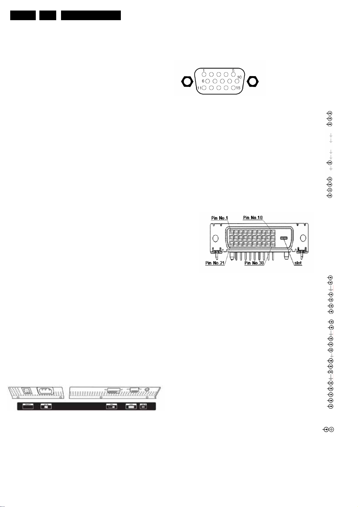
VGA:Video 2fh RGB In
Figure 1-2 VGA Connector
1 - Video Red 0.7 VPP / 75 ohm
2 - Video Green 0.7 V
3 - Video Blue 0.7 V
4 – n.c
5 –Ground Gnd
6 -Ground Red Gnd
7 -Ground
Green Gnd
8 -Ground Blue Gnd
9 - +5V_DC +5V
10 -Gnd Sync Gnd
11 - n.c.
12 - DDC_SDA DDC data
13 - H-sync 0 - 5V
14 - V-sync 0 - 5V
15 - DDC_SCL DDC clock
DVI Digital Video-In
PP / 75 ohm
PP / 75 ohm
DC
1.1.3 Miscellaneous
Power supply:
-AC Power voltage (VAC) : 90-264V
-AC Power frequency (Hz) : 47~63Hz
Ambient conditions:
-Temperature range : 0~35°C
- Maximum humidity : 10%~90%
Power consumption
- Normal operation : 210 W
- Stand-by: < 5 W
Dimensions (WxHxD mm) :617.7*1017.4*210.0
Weight (kg) :20.5Kg
1.2 Connections
1.2.1 Rear I/O Connections
Figure 1-1 back connections
1 TMDS Data 2- Data channel
2 TMDS Data 2+ Data channel
3 TMDS Data 2/4 shield GND
4 TMDS Data 4- Data channel
5 TMDS Data 4+ Data channel
6 DDC Clock DDC Clock
7 DDC Data DDC Data
8 N.C
9 TMDS Data 1- Data channel
10 TMDS Data 1+ Data channel
11 TMDS Data 1/3 shield
12 TMDS Data 3- Data channel
13 TMDS Data 3+ Data channel
14 +5V
15 Ground ( For +5V) GND
16 Hot Plug Detect Hot Plug Detect
17 TMDS Data 0- Data channel
18 TMDS Data 0+ Data channel
19 TMDS Data 0/5 shield GND
20 TMDS Data 5- Data channel
21 TMDS Data 5+ Data Channel
22 TMDS Clock shield Data channel
23 TMDS Clock+ Data channel
24 TMDS Clock Data channel
Audio-In
Gn Stereo R/L Channels 500mVrms/22K ohm
Page 3
Technical Specifications, Connections, and Chassis Overview
EN 2
1.
MQC1.OA LA
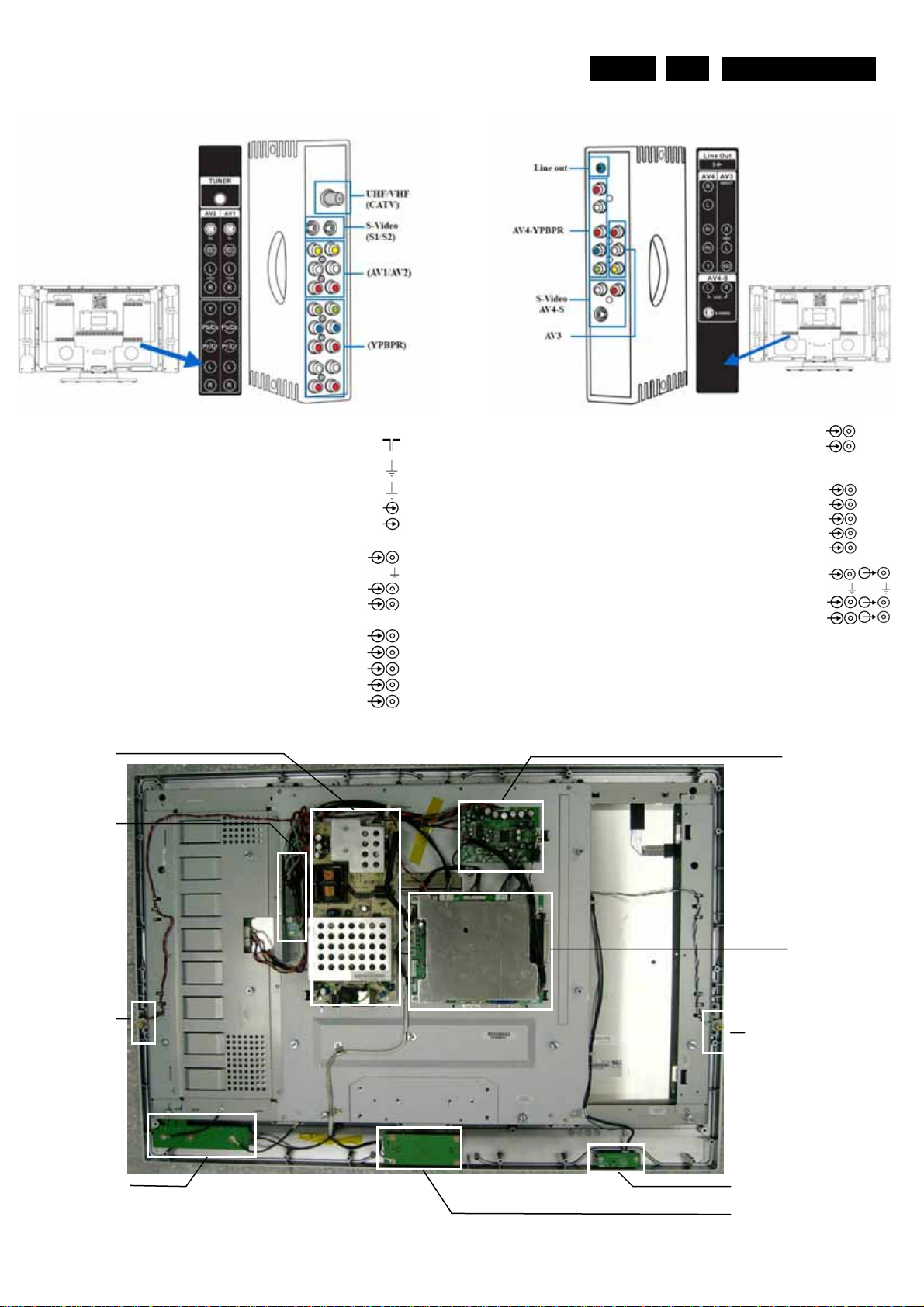
1.2.2 Right I/O Connections
Aerial-In
-F-type 75ohm
AV1-S1/AV2-S2: S-Video 1Fh Y/C-In
1 -Ground Y Gnd
2 -Ground C Gnd
3 -Video Y 1Vpp/75 ohm
4 -Video C 0.3Vpp/75 ohm
AV1/AV2 Video In, Audio In
1 -Audio R 0.5 Vrms/10Kohm
2 -Gnd CVBS Gnd
3 -Video CVBS 1Vpp/75 ohm
4 -Audio L 0.5 Vrms/10Kohm
YPBPR1/YPBPR2
Wh….-Audio L 0.5 Vrms/10Kohm
Rd….-Audio R 0.5 Vrms/10Kohm
Bu Video Pb 0.7 Vpp/75 ohm
Rd Video Pr 0.7 Vpp/75 ohm
Gn Video Y 1Vpp/75 ohm
1.3 Chassis overview
1.2.3 Left I/O Connections
Line-out
1 Audio R 0.5 Vrms/10Kohm
2 Audio L 0.5 Vrms/10Kohm
AV4-YPBPR
AV4-YPBPR
Wh….-Audio R 0.5 Vrms/10Kohm
Rd….-Audio R 0.5 Vrms/10Kohm
Bu Video Pb 0.7 Vpp/75 ohm
Rd Video Pr 0.7 Vpp/75 ohm
Gn Video Y 1Vpp/75 ohm
AV3 Video In/out /Audio in/out
1 -Audio R 0.5 Vrms/10Kohm
2 -Gnd CVBS Gnd
3 -Video CVBS 1Vpp/75 ohm
4 -Audio L 0.5 Vrms/10Kohm
AV4 S-Video In/Audio In
1 -Ground Y Gnd
2 -Ground C Gnd
3 -Video Y 1Vpp/75 ohm
4 -Video C 0.3Vpp/75 ohm
Rd….-Audio R 0.5 Vrms/10Kohm
Wh….-Audio L 0.5 Vrms/10Kohm
Power Board
Interface Board
Speaker Board
Button Board
Audio Board
Main Board
Speaker Board
Earphone Board
Power Key Board
Page 4
EN 3
Safety Instructions, Warnings, and Notes
2.
MQC1.OA LA
2. Safety Instructions, Warnings, and Notes
2.1 Safety Instructions
Safety regulations require that during a repair:
• Connect the set to the AC Power via an isolation
transformer (> 800 VA).
• Replace safety components, indicated by the symbol
only by components identical to the original ones. Any
other component substitution (other than original type) may
increase risk of fire or electrical shock hazard.
Safety regulations require that after a repair, the set must be
returned in its original condition. Pay in particular attention to
the following points:
• Route the wire trees correctly and fix them with the
mounted cable clamps.
• Check the insulation of the AC Power lead for external
damage.
• Check the strain relief of the AC Power cord for proper
function.
• Check the electrical DC resistance between the AC Power
plug and the secondary side (only for sets which have a AC
Power isolated power supply):
1. Unplug the AC Power cord and connect a wire
between the two pins of the AC Power plug.
2. Set the AC Power switch to the "on" position (keep the
AC Power cord unplugged!).
3. Measure the resistance value between the pins of the
AC Power plug and the metal shielding of the tuner or
the aerial connection on the set. The reading should be
between 4.5 Mohm and 12 Mohm.
4. Switch "off" the set, and remove the wire between the
two pins of the AC Power plug.
• Check the cabinet for defects, to avoid touching of any
inner parts by the customer.
,
2.2 Warnings
• All ICs and many other semiconductors are susceptible to
electrostatic discharges (ESD
during repair can reduce life drastically. Make sure that,
during repair, you are connected with the same potential as
the mass of the set by a wristband with resistance. Keep
components and tools also at this same potential. Available
ESD protection equipment:
– Complete kit ESD3 (small tablemat, wristband,
connection box, extension cable and earth cable) 4822
310 10671.
– Wristband tester 4822 344 13999.
• Be careful during measurements in the high voltage
section.
• Never replace modules or other components while the unit
is switched "on".
• When you align the set, use plastic rather than metal tools.
This will prevent any short circuits and the danger of a
circuit becoming unstable.
). Careless handling
2.3 Notes
2.3.1 General
• Measure the voltages and waveforms with regard to the
chassis (= tuner) ground ( ), or hot ground ( ), depending
on the tested area of circuitry. The voltages and waveforms
shown in the diagrams are indicative. Measure them in the
Service Default Mode (see chapter 5) with a color bar
signal and stereo sound (L: 3 kHz, R: 1 kHz unless stated
otherwise) and picture carrier at 475.25 MHz for PAL, or
61.25 MHz for NTSC (channel 3).
• Where necessary, measure the waveforms and voltages
with ( ) and without ( ) aerial signal. Measure the
voltages in the power supply section both in normal
operation ( ) and in stand-by ( ). These values are
indicated by means of the appropriate symbols.
• The semiconductors indicated in the circuit diagram and in
the parts lists, are interchangeable per position with the
semiconductors in the unit, irrespective of the type
indication on these semiconductors.
• Manufactured under license from Dolby Laboratories.
“Dolby” and the “double-D symbol”, are trademarks of
Dolby Laboratories.
2.3.2 Schematic Notes
• All resistor values are in ohms and the value multiplier is
often used to indicate the decimal point location (e.g. 2K2
indicates 2.2 Kohm).
• Resistor values with no multiplier may be indicated with
either an "E" or an "R" (e.g. 220E or 220R indicates 220
ohm).
• All capacitor values are given in micro-farads (µ= x10
nano-farads (n= x10
• Capacitor values may also use the value multiplier as the
decimal point indication (e.g. 2p2 indicates 2.2 pF).
• An "asterisk" (*) indicates component usage varies. Refer
to the diversity tables for the correct values.
• The correct component values are listed in the Electrical
Replacement Parts List. Therefore, always check this list
when there is any doubt.
2.3.3 Rework on BGA (Ball Grid Array) ICs
General
Although (LF)BGA assembly yields are very high, there may
still be a requirement for component rework. By rework, we
mean the process of removing the component from the PWB
and replacing it with a new component. If an (LF)BGA is
removed from a PWB, the solder balls of the component are
deformed drastically so the removed (LF)BGA has to be
discarded.
Device Removal
As is the case with any component that, it is essential when
removing an (LF)BGA, the board, tracks, solder lands, or
surrounding components are not damaged. To remove an
(LF)BGA, the board must be uniformly heated to a temperature
close to the reflow soldering temperature. A uniform
temperature reduces the chance of warping the PWB.
To do this, we recommend that the board is heated until it is
certain that all the joints are molten. Then carefully pull the
component off the board with a vacuum nozzle. For the
appropriate temperature profiles, see the IC data sheet.
Area Preparation
When the component has been removed, the vacant IC area
must be cleaned before replacing the (LF)BGA.
Removing an IC often leaves varying amounts of solder on the
mounting lands. This excessive solder can be removed with
either a solder sucker or solder wick. The remaining flux can be
removed with a brush and cleaning agent.
After the board is properly cleaned and inspected, apply flux on
the solder lands and on the connection balls of the (LF)BGA.
Note: Do not apply solder paste, as this has shown to result in
problems during re-soldering.
-9
), or pico-farads (p= x10
-6
-12
),
).
Page 5
Device Replacement
The last step in the repair process is to solder the new
component on the board. Ideally, the (LF)BGA should be
aligned under a microscope or magnifying glass. If this is not
possible, try to align the (LF)BGA with any board markers.
To reflow the solder, apply a temperature profile according to
the IC data sheet. So as not to damage neighboring
components, it may be necessary to reduce some
temperatures and times.
More Information
For more information on how to handle BGA devices, visit this
www.atyourservice.ce.philips.com (needs subscription,
URL:
not available for all regions). After login, select “Magazine”,
then go to “Workshop Information”. Here you will find
Information on how to deal with BGA-ICs.
2.3.4 Lead Free Solder
Philips CE is going to produce lead-free sets (PBF) from
1.1.2005 onwards.
Lead-free sets will be indicated by the PHILIPS-lead-free logo
on the Printed Wiring Boards (PWB):
Figure 2-1 Lead-free logo
This sign normally has a diameter of 6 mm, but if there is less
space on a board also 3 mm is possible.
In case of doubt wether the board is lead-free or not (or with
mixed technologies), you can use the following method:
• Always use the highest temperature to solder, when using
SAC305 (see also instructions below).
• De-solder thoroughly (clean solder joints to avoid mix of
two alloys).
Caution: For BGA-ICs, you must use the correct temperature
profile,which is coupled to the 12NC. For an overview of these
profiles, visit the website
You will find this and more technical information within the
"Magazine", chapter "Workshop information".
For additional questions please contact your local repair-helpdesk.
http://www.atyourservice.ce.philips.com/
EN 4 Directions for Use MQC1.OA LA
3.
Due to lead-free technology some rules have to be respected
by the workshop during a repair:
• Use only lead-free soldering tin Philips SAC305 with order
code 0622 149 00106. If lead-free solder paste is required,
please contact the manufacturer of your soldering
equipment. In general, use of solder paste within
workshops should be avoided because paste is not easy to
store and to handle.
• Use only adequate solder tools applicable for lead-free
soldering tin. The solder tool must be able
– To reach at least a solder-tip temperature of 400°C.
– To stabilise the adjusted temperature at the solder-tip.
– To exchange solder-tips for different applications.
• Adjust your solder tool so that a temperature around 360°C
-380°C is reached and stabilised at the solder joint.
Heating time of the solder-joint should not exceed ~ 4 sec.
Avoid temperatures above 400°C, otherwise wear-out of
tips will rise drastically and flux-fluid will be destroyed. To
avoid wear-out of tips, switch “off” unused equipment or
reduce heat.
• Mix of lead-free soldering tin/parts with leaded soldering
tin/parts is possible but PHILIPS recommends strongly to
avoid mixed regimes. If not to avoid, clean carefully the
solder-joint from old tin and re-solder with new tin.
• Use only original spare-parts listed in the Service-Manuals.
Not listed standard material (commodities) has to be
purchased at external companies.
• Special information for lead-free BGA ICs: these ICs will be
delivered in so-called "dry-packaging" to protect the IC
against moisture. This packaging may only be opened
short before it is used (soldered). Otherwise the body of the
IC gets "wet" inside and during the heating time the
structure of the IC will be destroyed due to high (steam)pressure inside the body. If the packaging was opened
before usage, the IC has to be heated up for some hours
(around 90°C) for drying (think of ESD-protection !).
Do not re-use BGAs at all!
• For sets produced before 1.1.2005, containing leaded
soldering tin and components, all needed spare parts will
be available till the end of the service period. For the repair
of such sets nothing changes.
2.3.5 Practical Service Precautions
• It makes sense to avoid exposure to electrical shock.
While some sources are expected to have a possible
dangerous impact, others of quite high potential are of
limited current and are sometimes held in less regard.
• Always respect voltages. While some may not be
dangerous in themselves, they can cause unexpected
reactions - reactions that are best avoided. Before reaching
into a powered TV set, it is best to test the high voltage
insulation. It is easy to do, and is a good service precaution.
3. Directions for Use
You can download this information from the following websites:
http://www.philips.com/support
http://www.p4c.philips.com
Page 6
Mechanical Instructions
EN 5
4.
MQC1.OA LA
4. Mechanical Instructions
Index of this chapter:
4.1 Cable Dressing
Service Positions
4.2
4.3 ASSY/PCBA Removal
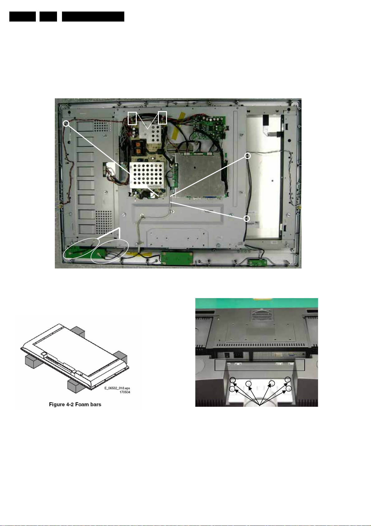
4.1 Cable Dressing
4.2 Service Positions
4.2.1 Foam Bars
67
68
69
4.2.2 Stands
The foam bars (order code 3122 785 90580 for two pieces) can
be used for all types and sizes of Flat TVs. By laying the TV
face down on the (ESD protective) foam bars, a stable situation
is created to perform measurements and alignments.
By placing a mirror under the TV, you can monitor the screen.
70
Figure 4-3 Stands
The stands can be mounted with the back cover removed or
still left on. So, the stand can be used to store products or to do
measurements. It is also very suitable to perform duration tests
without taking much space, without having the risk of overheating
,or the risk of products falling. The stands can be mounted and
removed quick and easy with use of the delivered screws that
can be tightened and loosened manually without the use of tools.
See figure above.
Note: Only use the delivered screws to mount the monitor to
the stands
Page 7
Mechanical Instructions
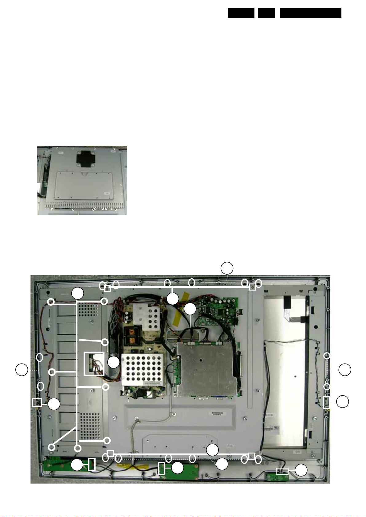
4.3 Assy/Panel removal
4.3.1 IO/Sub IO
Warning: Disconnect the AC Power cord before you open the
set.
1. Place the TV set upside down on a table top, using the
foam bars (see part "Foam Bars").
Caution: do not put pressure on the display, but let the
monitor lean on the speakers or the Front cover.
2. Remove M3*12(4 pieces) from IO Box and Sub-IO Box
4.3.2 R&L Speaker/Fan cover/Back cover
1. Remove T3*8 (4 pieces) screws from the Fan cover
2. Remove all T4*12(16 pieces) screws from the Back cover.
3. Than, remove the T4*24(6 pieces) from R/L speaker
4. Lift the back cover from the set. Make sure that wires and
flat foils are not damaged during the back cover removal.
4.3.3 Wall mount
1. Remove T3*5(4 pieces) screws from down of wall mount
2. Remove M3*4(4 pieces) screw from top of wall mount
3. Remove Io Nut(4 pieces) screw from down of wall mount
4. Remove 4-40(2 pieces) screw from right side of wall mount
5. Lift the wall mount from chassis. Make sure wires are not
damaged during the back cover removal.
4.3.11 LCD Panel
7
4.3.4 Main Board
1. Disconnect all cable from Base unit
2. Remove the fixation screws
3. Take out Main Board
4.3.5 Audio Board
1. Remove the fixation screws
2. Take out Main Board
4.3.6 Power Board
1. Remove the fixation screws
2. Take out Main Board
4.3.7 Interface Board
1. Remove the fixation screws
2. Take out Main Board
4.3.8 Power-Key Board
1. Remove the fixation screws
2. Take out Main Board
4.3.9 Earphone Board
1. Remove the fixation screws
2. Take out Main Board
4.3.10 Button Board
1. Remove the fixation screws
2. Take out Main Board and Bracket
10
6
11
EN 6
4.
MQC1.OA LA
8
4
9
2
3
11
1
1111
5
Page 8
EN 7
Mechanical Instructions
4.
MQC1.OA LA
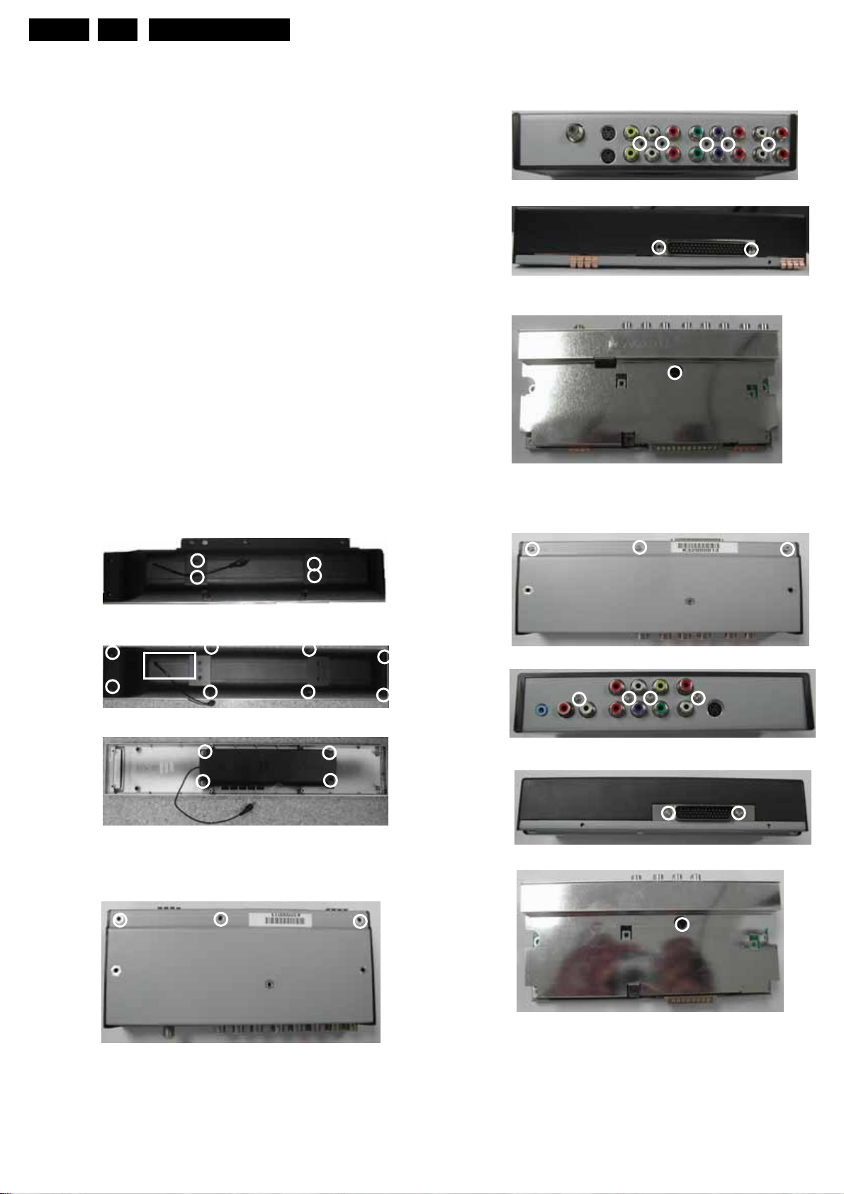
Disassembly
1. Place the TV set down on the foam bars. Place the
bars at the edges of the set, so they will support the
front frame and not only the glass plate!
2. Remove the Earphone cable (1), Button cable (2), Power key cable (3)
Speak L Cable (4), Speaker R cable (5) from all PCBA. Remove
LVDS cable from LCD panel (6)
3. Remove the eight M3*5 screws (7) from Inverter shielding
Lift the shielding and remove inverter cable (8)
4. Remove the two M3*5 screws (9) and two M3*4 screws (10)
Lift the PCB tray from the set. Make sure that wires and
flat foils are not damaged during the PCB tray removal.
5. Remove the sixteen T4*12 screws (11) from front cover
Lift the LCD panel from front cover.
6. Remove the ten M4*10 screws from Chassis-U, Chassis-R
Chassis-D, Chassis-L. Lift the LCD from Chassis.
2. Remove the 5 screws from shielding
3. Remove the 5 screws from shielding
4. Remove the screw from shielding
Assembly
To re-assemble the LCD panel, execute all processes
in reverse order.
Note:
.While re-assemble, make sure that all are placed and
And connected in their original position. See figure
“Cable dressing”
.Pay special attention not to damage the EMC foams at the
SSB shielding. Check that EMC foams are put correctly on
their places.
4.3.12 R,L speaker
Disassembly
1. Remove the four screws from speaker shielding
and lift the shielding
.
4.3.13 IO Assy
Disassembly
1. Remove the three screws form shielding.
2. Remove the eight screws from speaker back cover
and open the mylar then lift the speaker back cover.
2. Remove the 4 screws from shielding
3. Remove the four screws
3. Remove the 2 screws from shielding
4.3.13 Tune r Assy
Disassembly
1. Remove the three screws from shielding
4. Remove the screw from shielding
Page 9
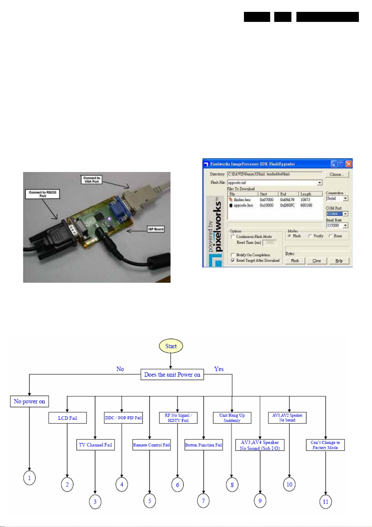
5 Service mode and Fault Finding
Service mode, Fault Finding
EN 8
5
MQC1.OA LA
Index if this chapter:
5.1Service Modes
5.1Fault Finding
5.1 Service Mode (update BIOS)
Purpose
. To update new version BIOS
Tools
. ISP Board
. RS232 cable
. VGA cable
. Software (Pixlworks)
5.2 Fault Finding
Purpose
.To find the fault
How to find fault
Setup
1. Off TV Pow e r
2. Process Pixlworks program
3. Choose appcode.inf
4. Check connection. Should be in serial
5. Check COM Port of R232
6. Check Baud Rate
7. Click Flash
8. Turn on the TV .The program will automatic
9. After few seconds, then screen will showing flash
completed. TV will power on itself
Page 10
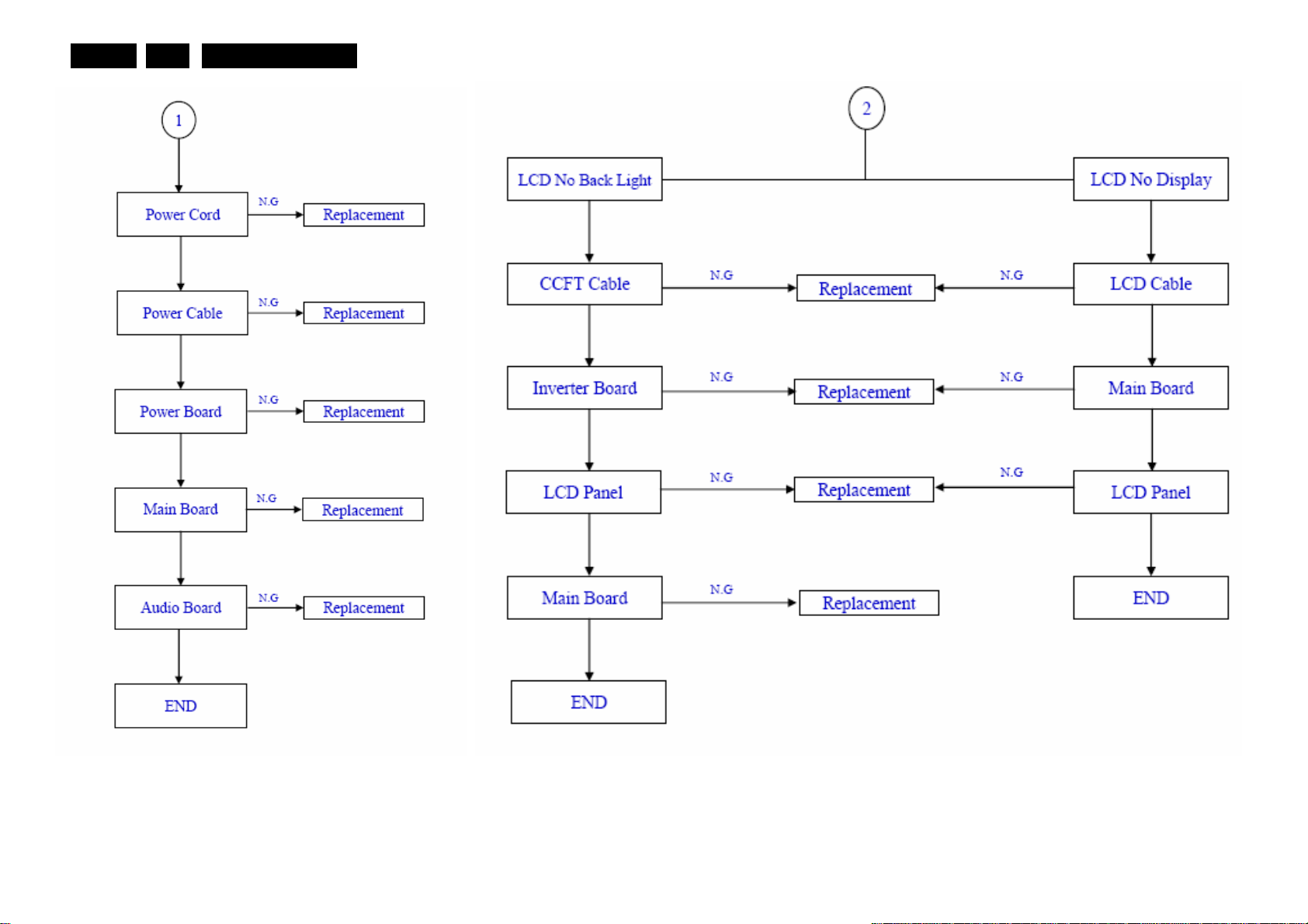
Service mode, Fault Finding
EN 9
5
MQC1.OA LA
Page 11
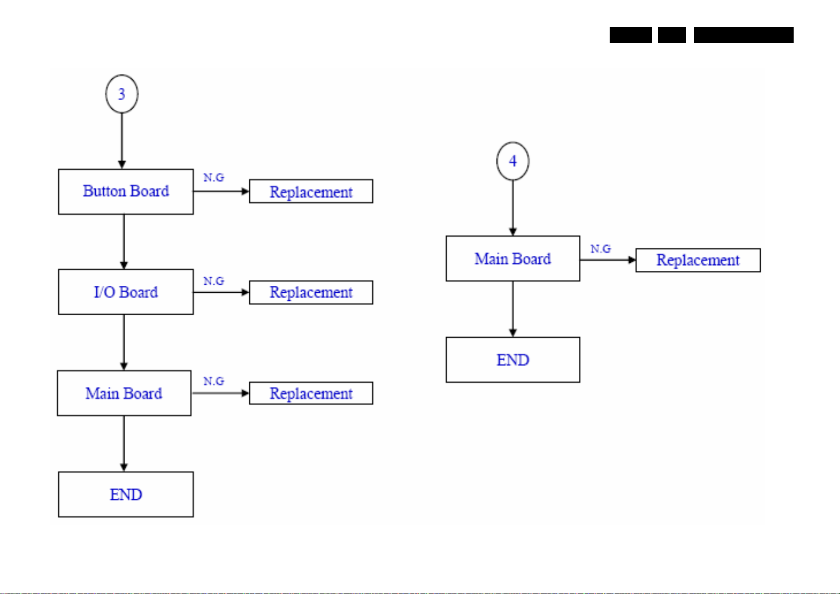
Service mode, Fault Finding
EN 10
5
MQC1.OA LA
Page 12
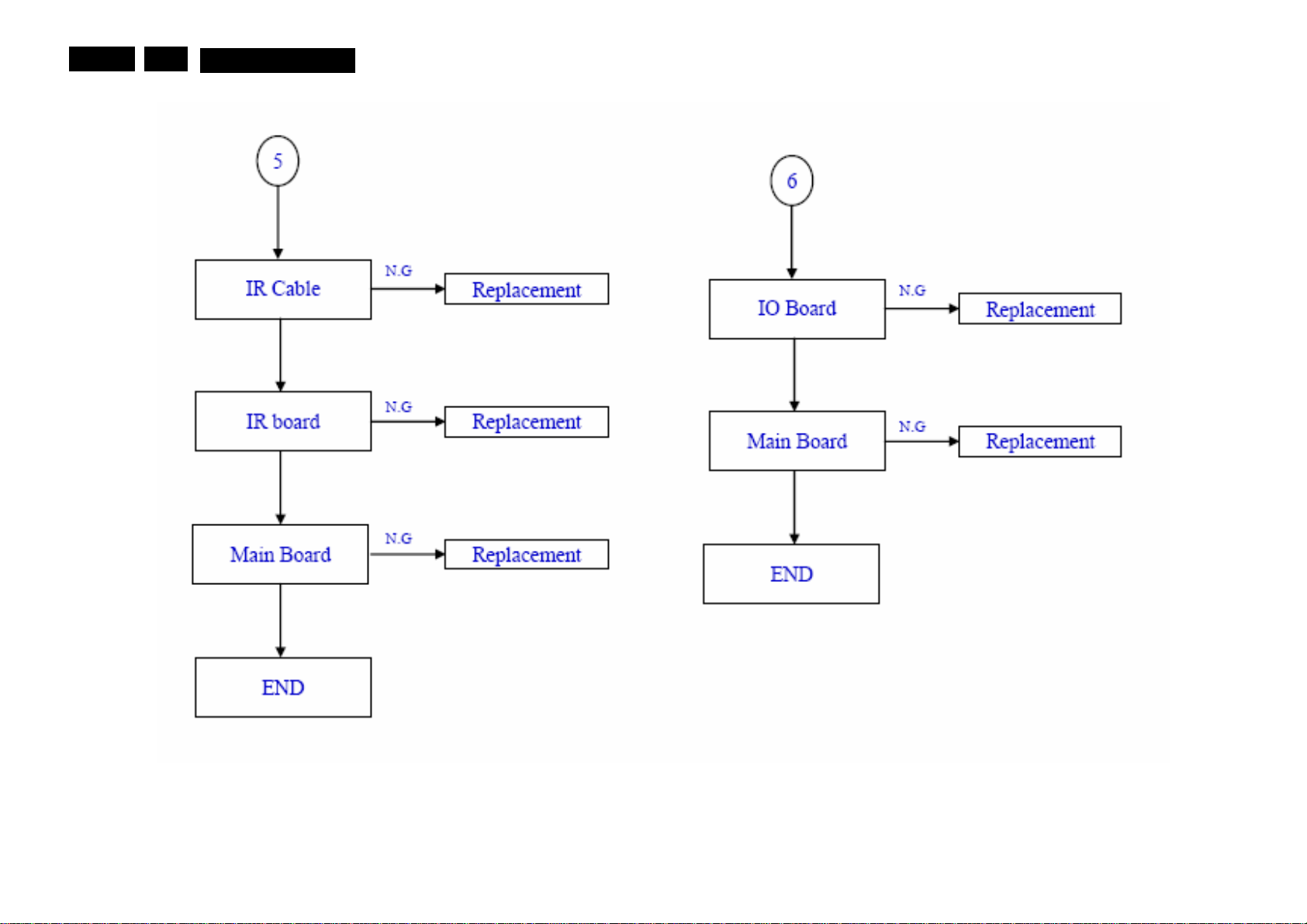
Service mode, Fault Finding
EN 11
5
MQC1.OA LA
Page 13
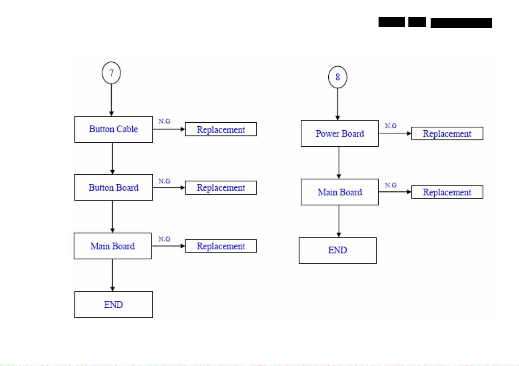
MQC1.OA LA Service mode, Fault Finding 5EN 12
Page 14
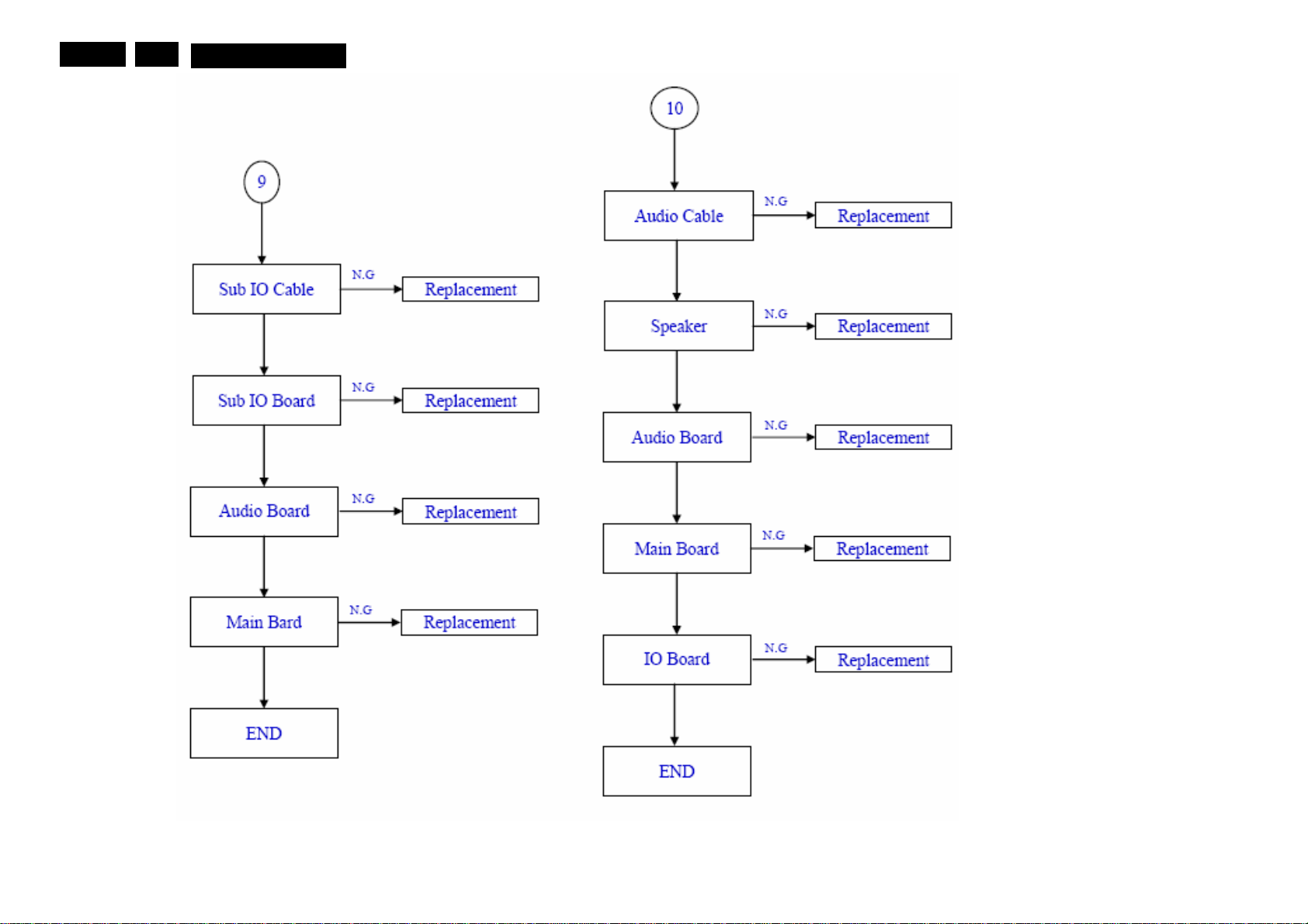
EN 13
5
MQC1.OA LA
Service mode, Fault Finding
Page 15
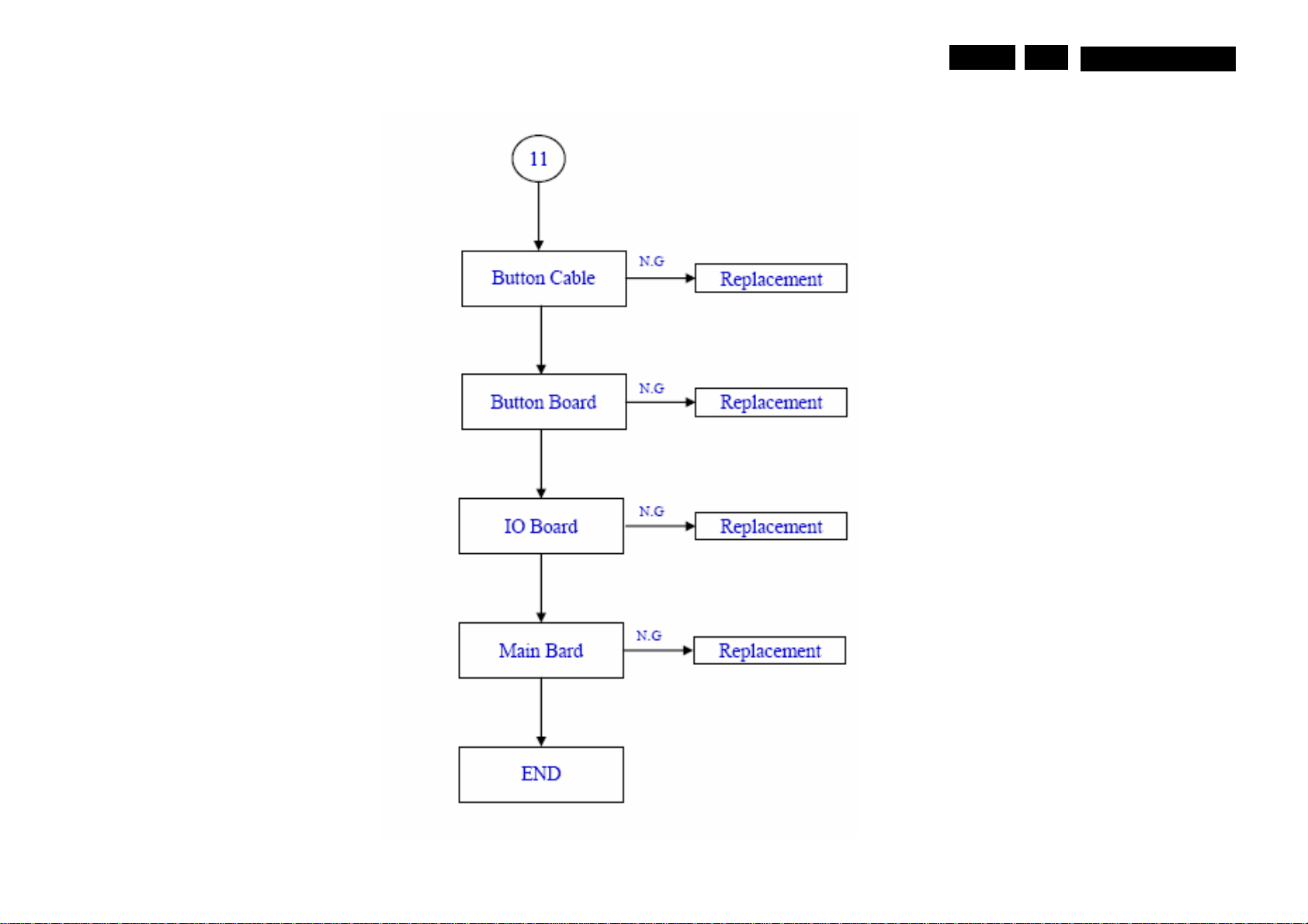
Service mode, Fault Finding
EN 14
5
MQC1.OA LA
Page 16
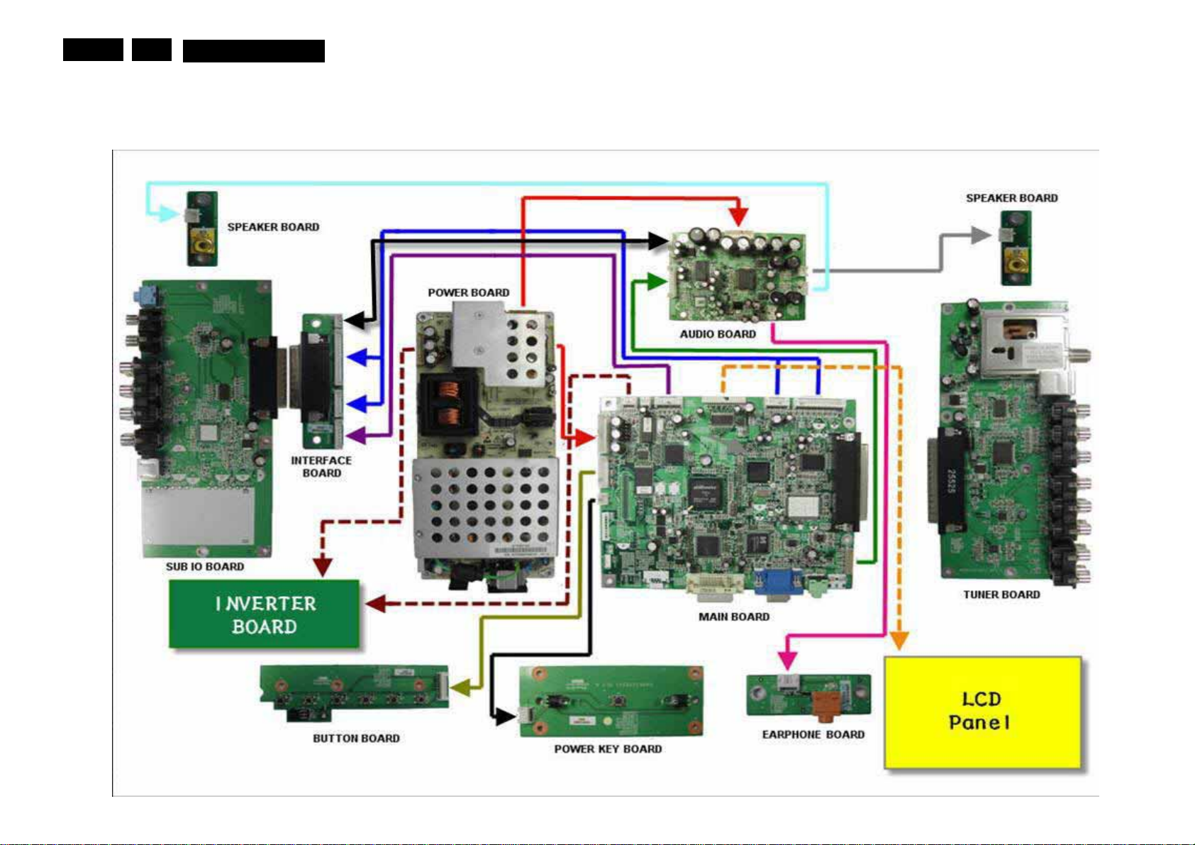
EN 15
6
MQC1.OA LA
6. Block Diagrams
Wiring Diagram
Block Diagrams
Page 17
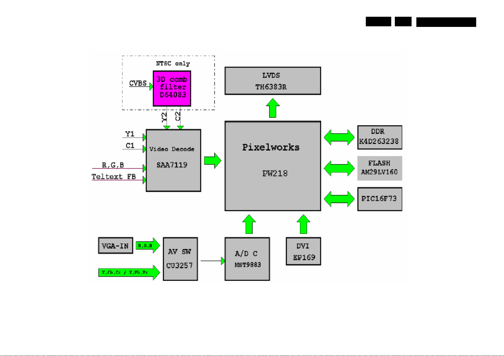
Main Board Block diagrams
MQC1.OA LA Block Diagrams 6EN 16
Page 18
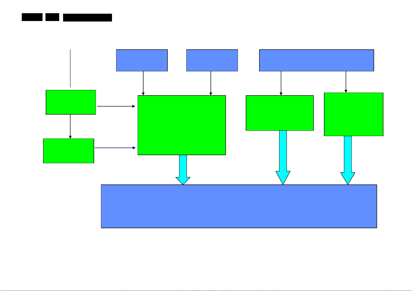
EN 17
Io Board Block diagrams
6
TV
MQC1.OA LA
signal
Block Diagrams
TV Tune r
TMQH6-011A
Audio Decoder
AN5832SA
TV Video
Audio
AV1 /AV2
Video& Audio Video
Video & Audio SW
Video & Audio SW
CVBS & YC
TA1218
TA1218
S1/S2
YUV Video
IO PORT
CU3257
YUV
YUV1/YUV2
SoundVideo
YUV Sound
74HCT4052_0
Page 19
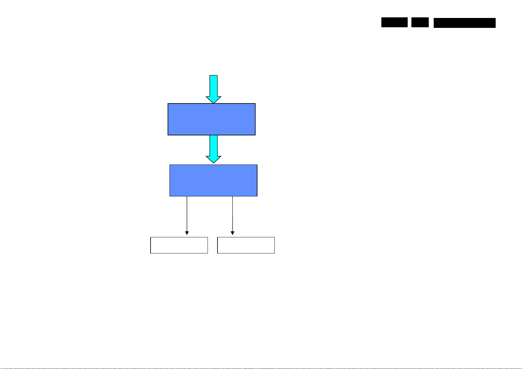
Audio board Block Diagrams
MQC1.OA LA Block Diagrams 6EN 18
Audio Processor
Audio Amplifier
SPEAKER-L SPEAKER-R
Page 20
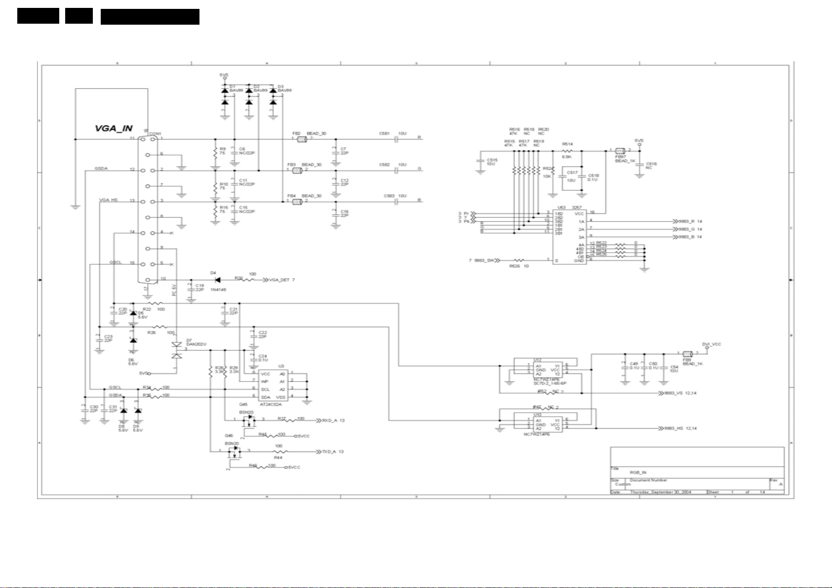
EN 19
7. Circuit Diagrams ,PCBA Layouts
MB
7
MQC1.OA LA
Circuit Diagrams, PCB Layouts
Page 21
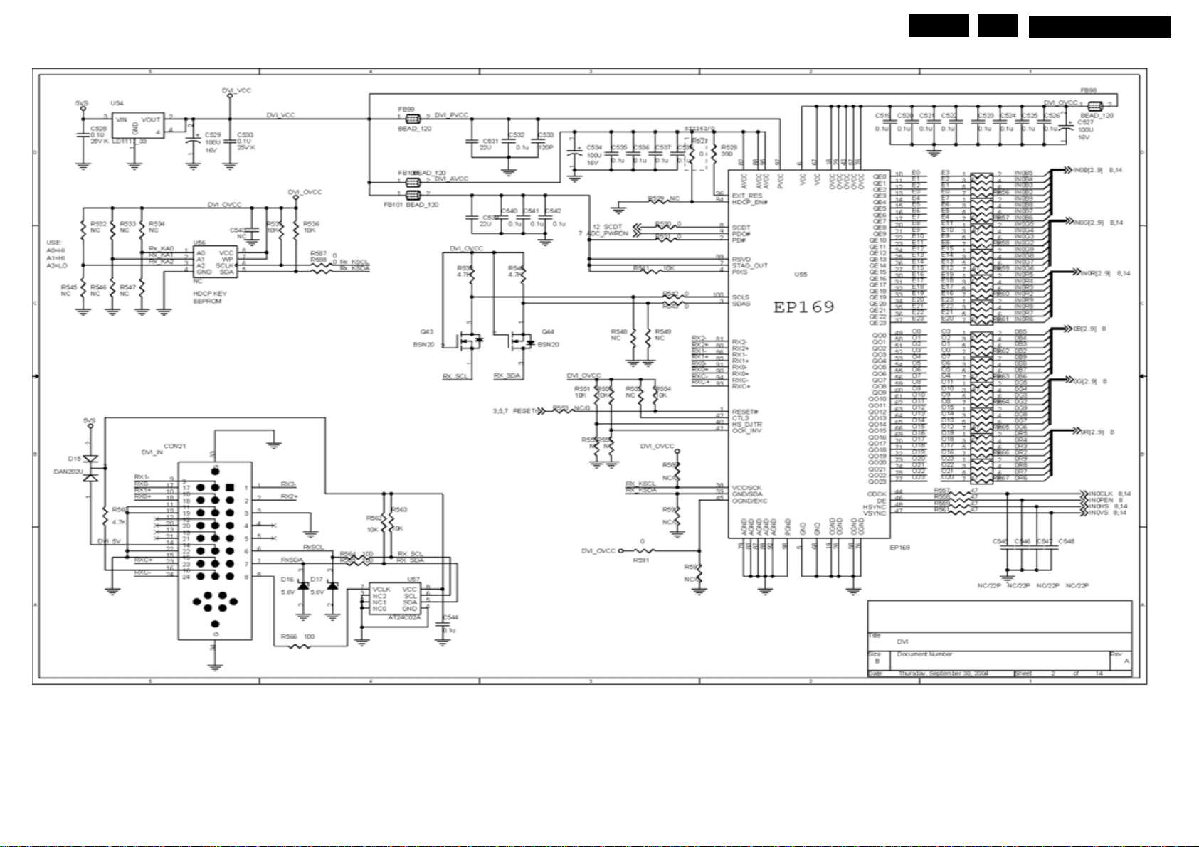
MQC1.OA LA Circuit Diagrams PCB Layout 7EN 20
Page 22
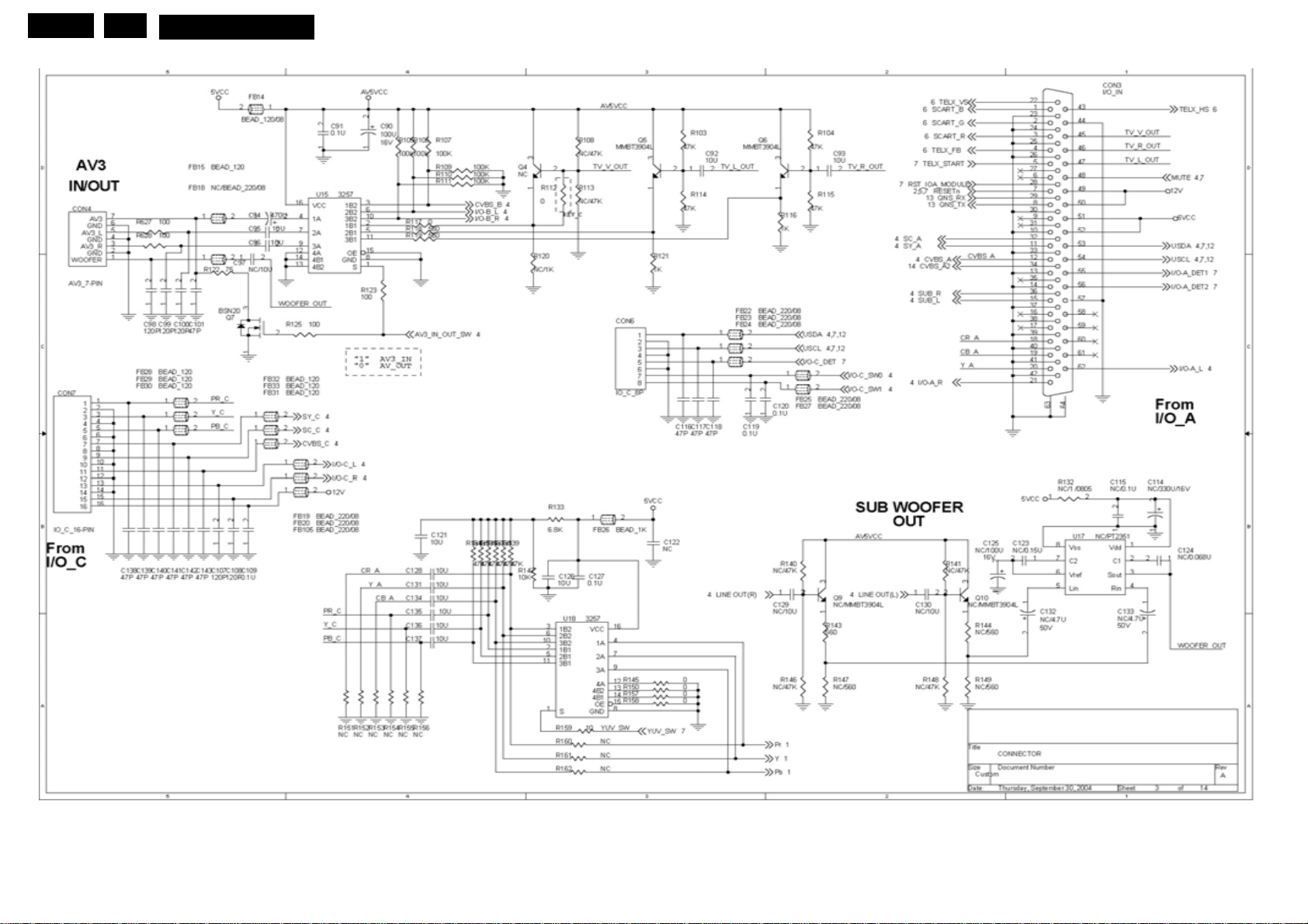
EN 21
7
MQC1.OA LA
Circuit Diagrams PCB Layouts
Page 23
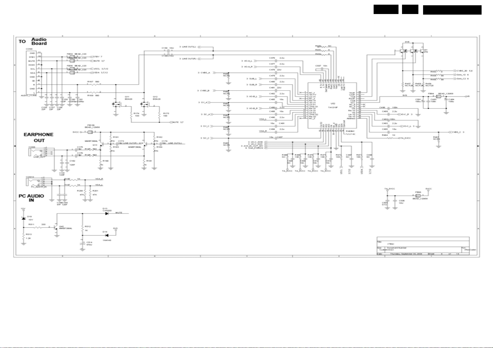
Circuit Diagrams PCB Layouts
EN 22
7
MQC1.OA LA
Page 24
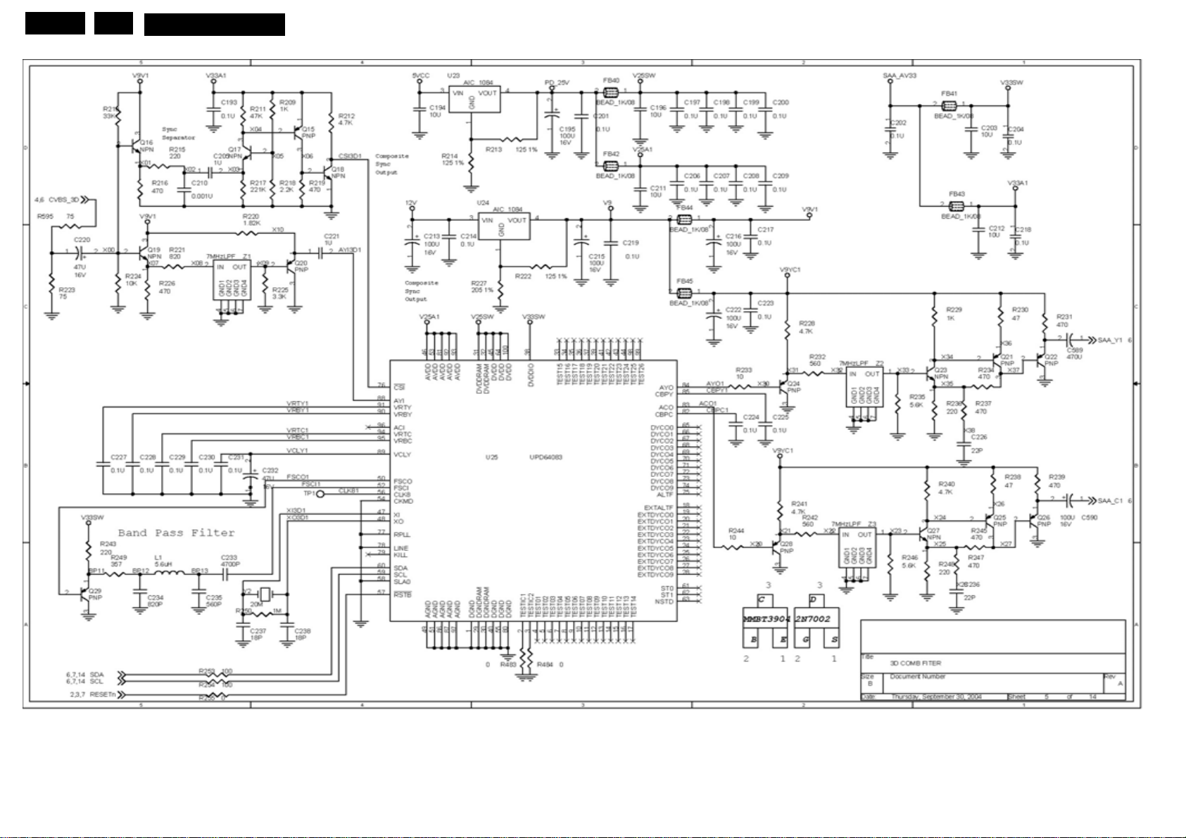
EN 23
7
MQC1.OA LA
Circuit Diagrams PCB Layouts
Page 25
EN 24
7
MQC1.OA LA Circuit Diagrams PCB Layouts
Page 26
EN 25
7
MQC1.OA LA
Circuit Diagrams PCB Layouts
Page 27
EN 26
7
MQC1.OA LA Circuit Diagrams PCB Layouts
Page 28
EN 27
7
MQC1.OA LA
Circuit Diagrams PCB Layouts
Page 29
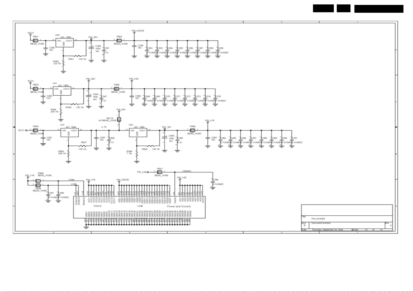
Circuit Diagrams PCB Layouts
EN 28
7
MQC1.OA LA
Page 30
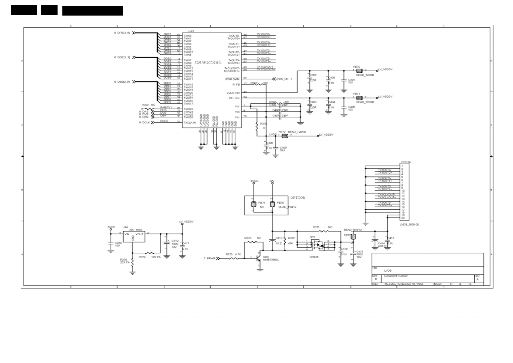
EN 29
7
MQC1.OA LA
Circuit Diagrams PCB Layouts
Page 31
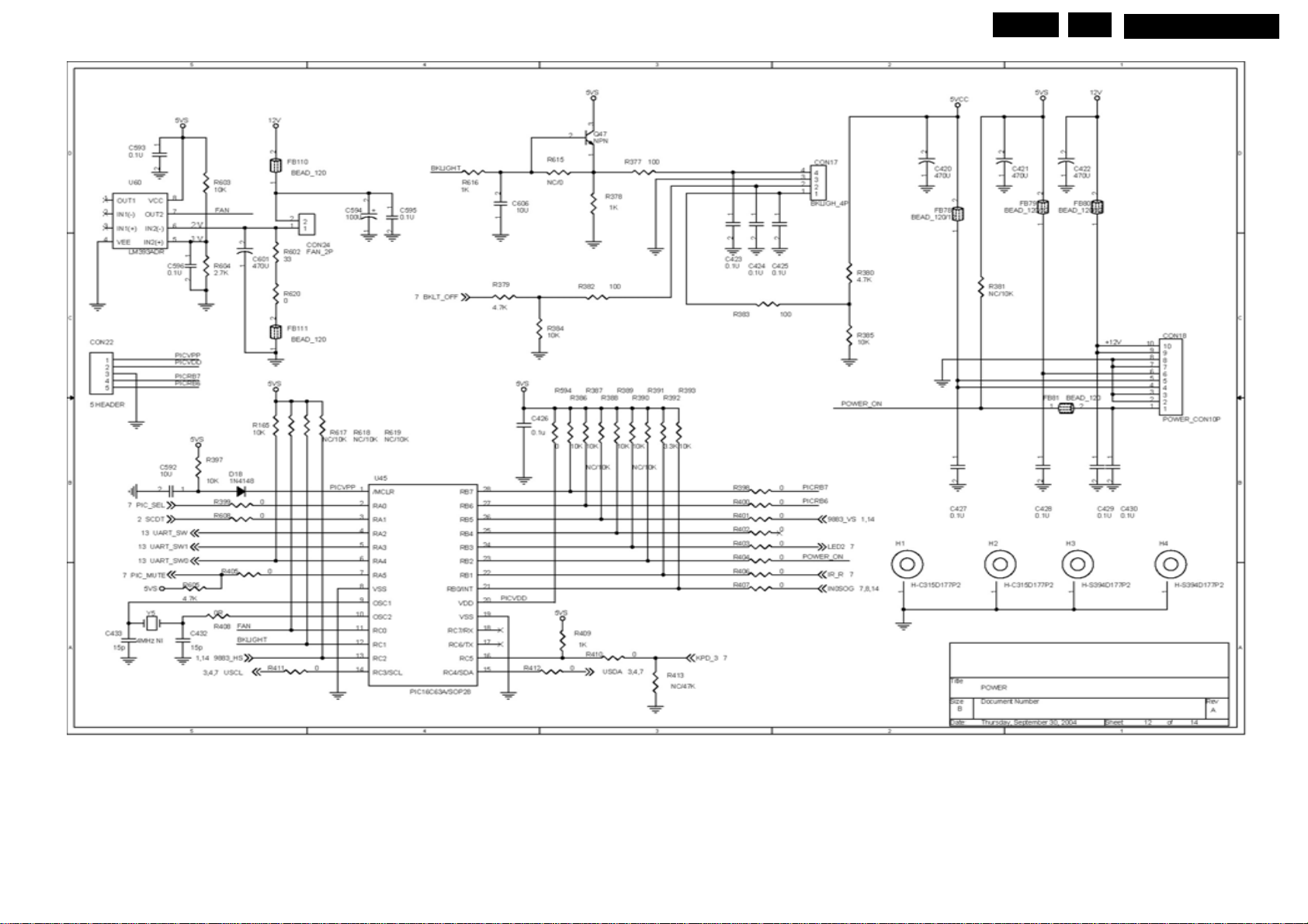
Circuit Diagrams PCB Layouts
EN 30
7
MQC1.OA LA
Page 32
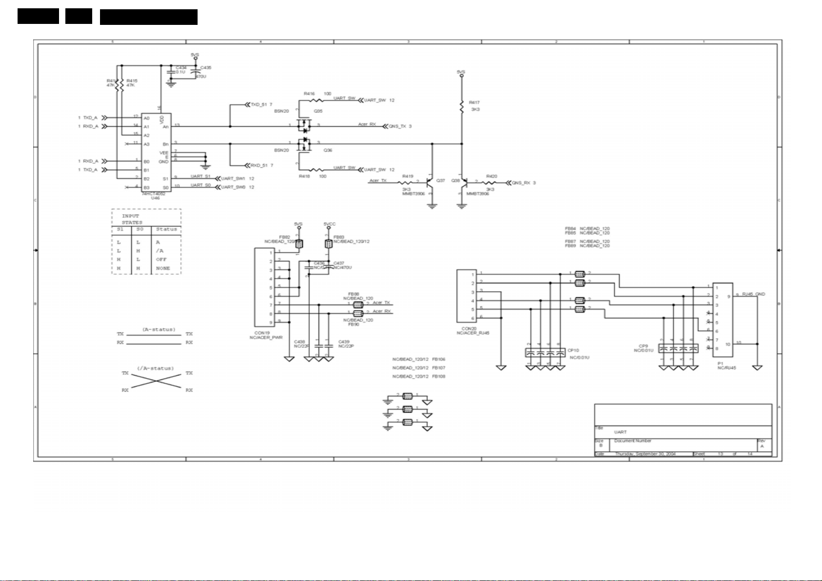
EN 31
7
MQC1.OA LA
Circuit Diagrams PCB Layouts
Page 33
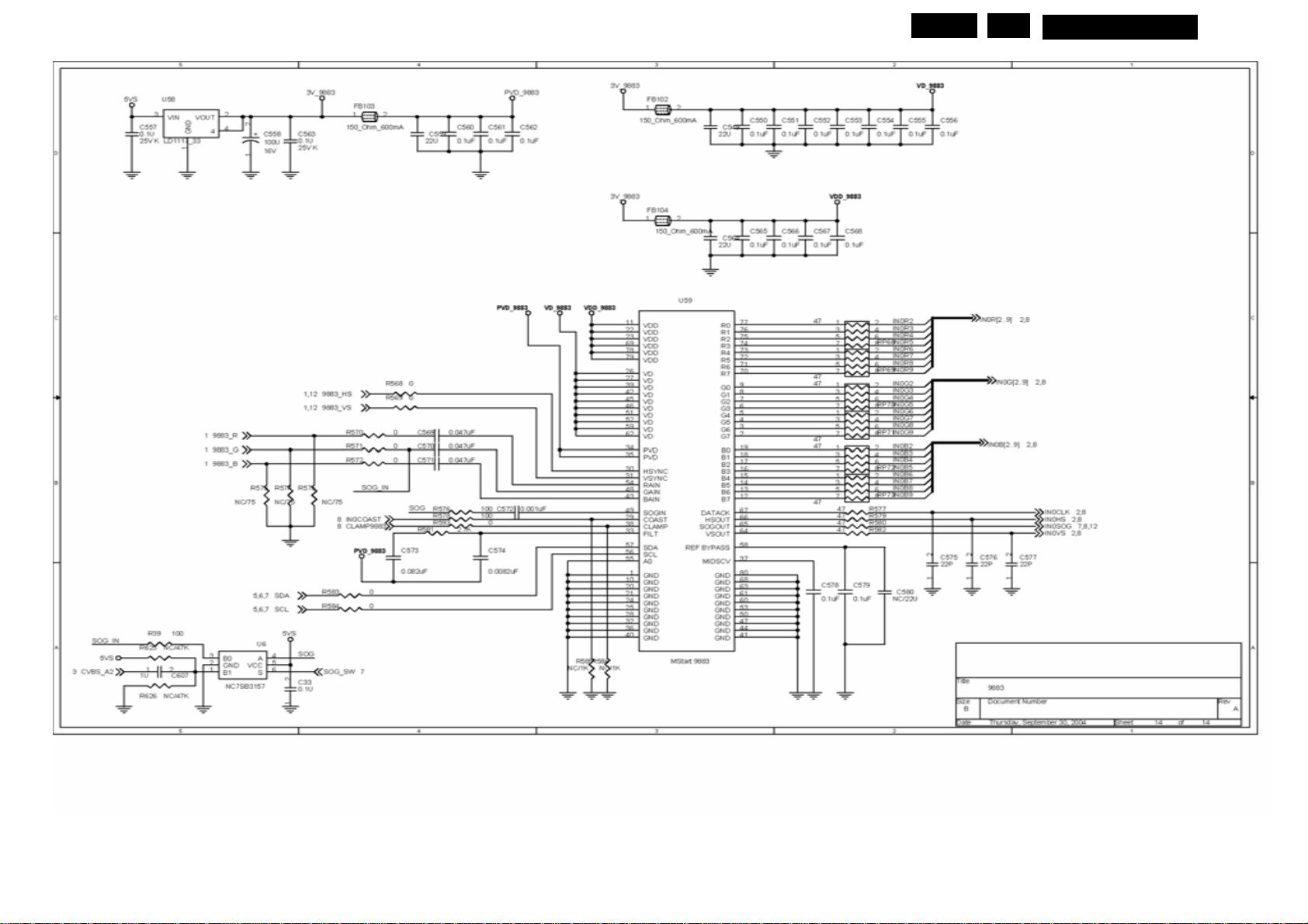
Circuit Diagrams PCB Layouts
EN 32
7
MQC1.OA LA
Page 34
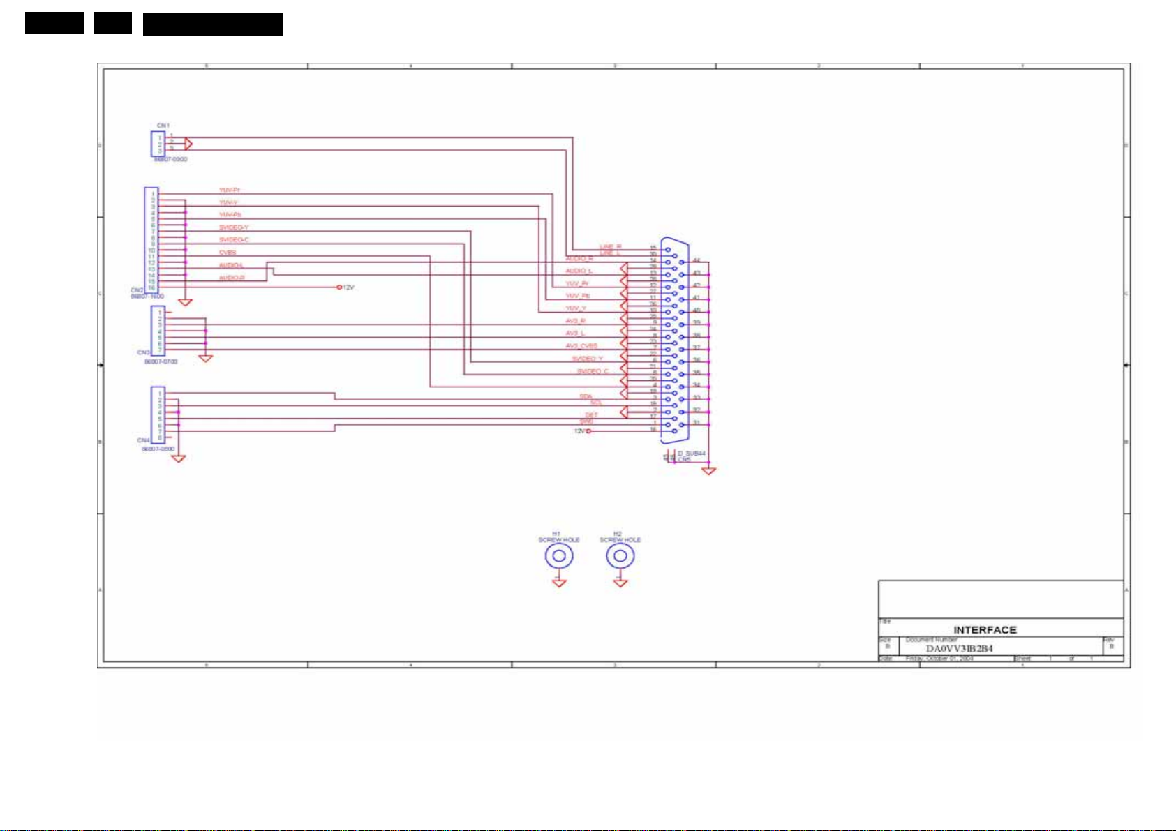
EN 33
7
Interface Board
MQC1.OA LA
Circuit Diagrams PCB Layouts
Page 35
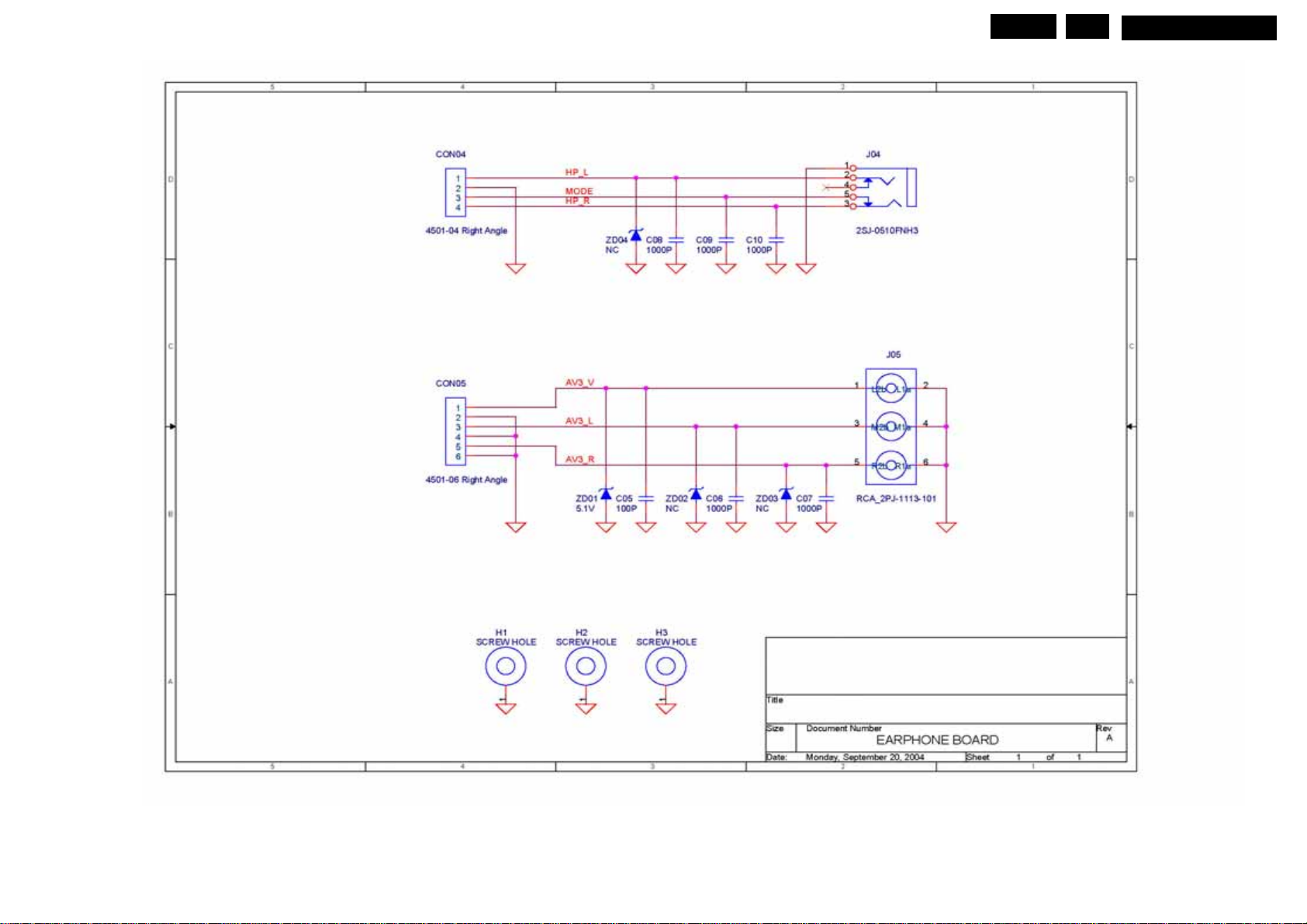
Earphone Board
Circuit Diagrams PCB Layouts
EN 34
7
MQC1.OA LA
Page 36
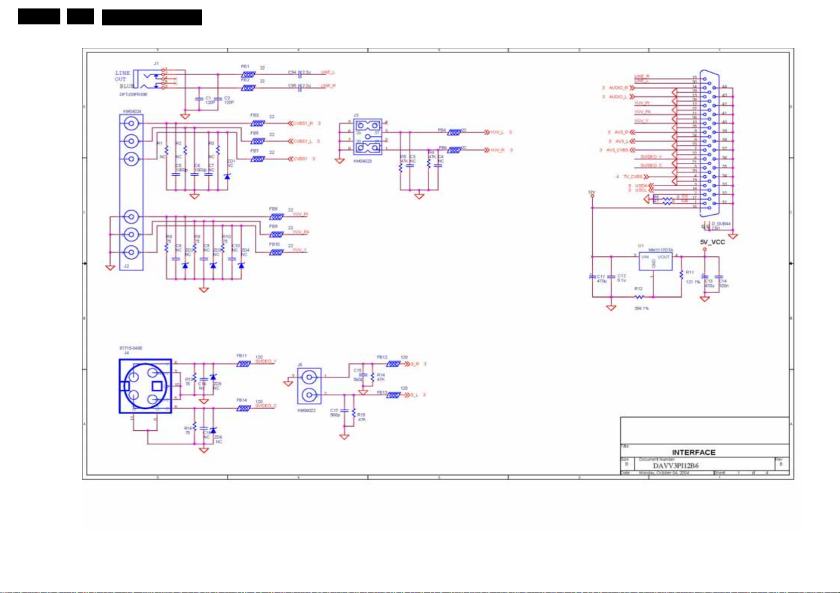
EN 35
Io Board
7
MQC1.OA LA
Circuit Diagrams PCB Layouts
Page 37
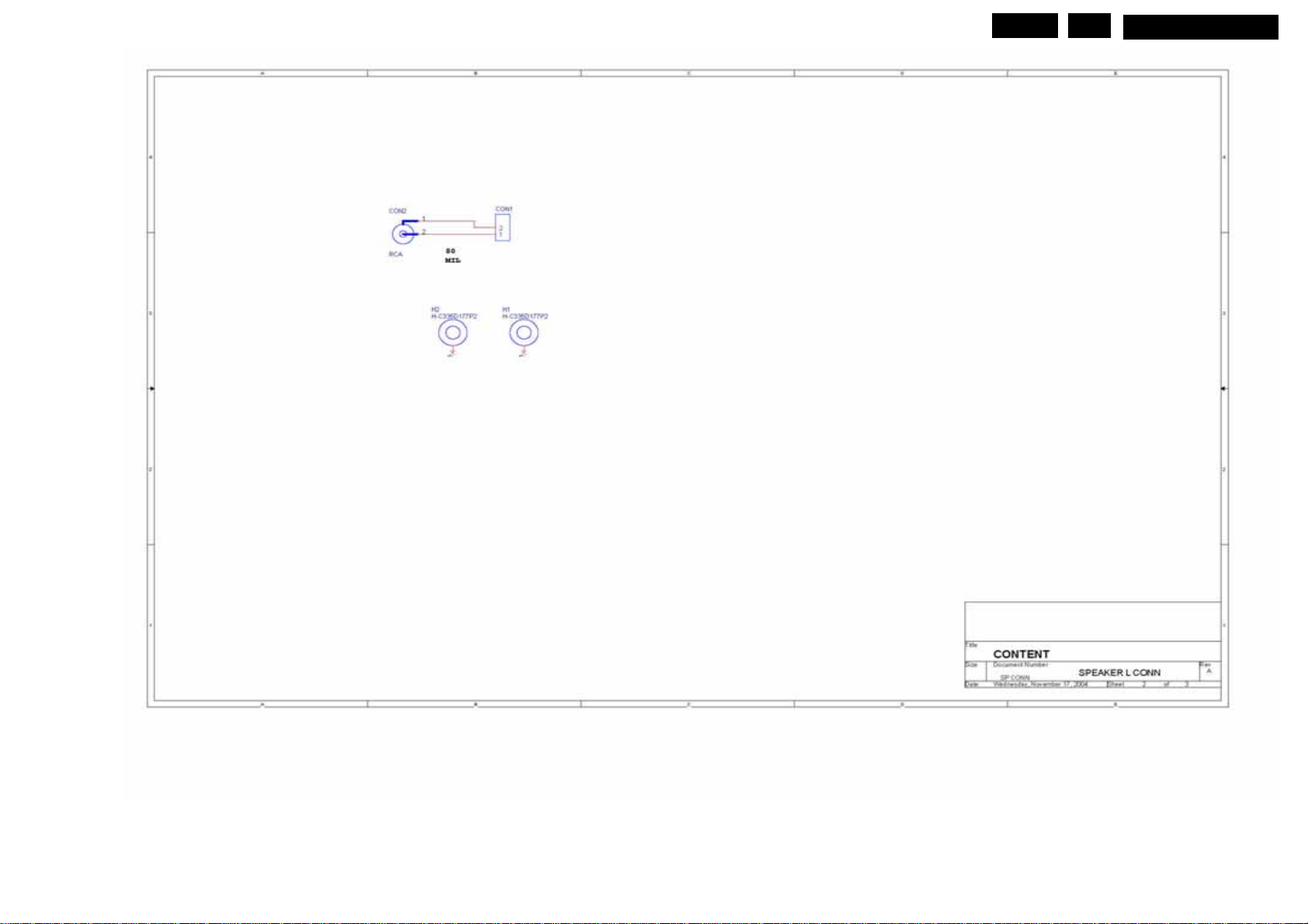
Speak Board
Circuit Diagrams PCB Layouts
EN 36
7
MQC1.OA LA
Page 38
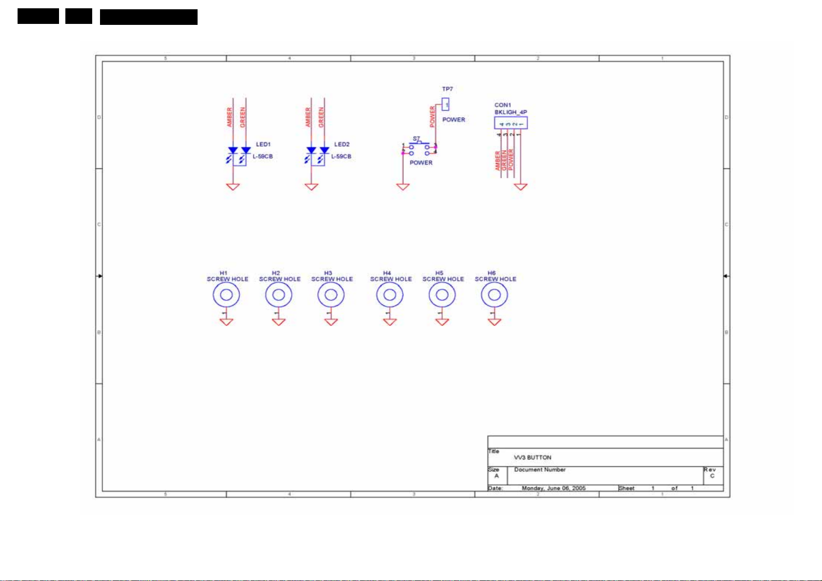
EN 37
7
Power-Key Board
MQC1.OA LA
Circuit Diagrams PCB Layouts
Page 39
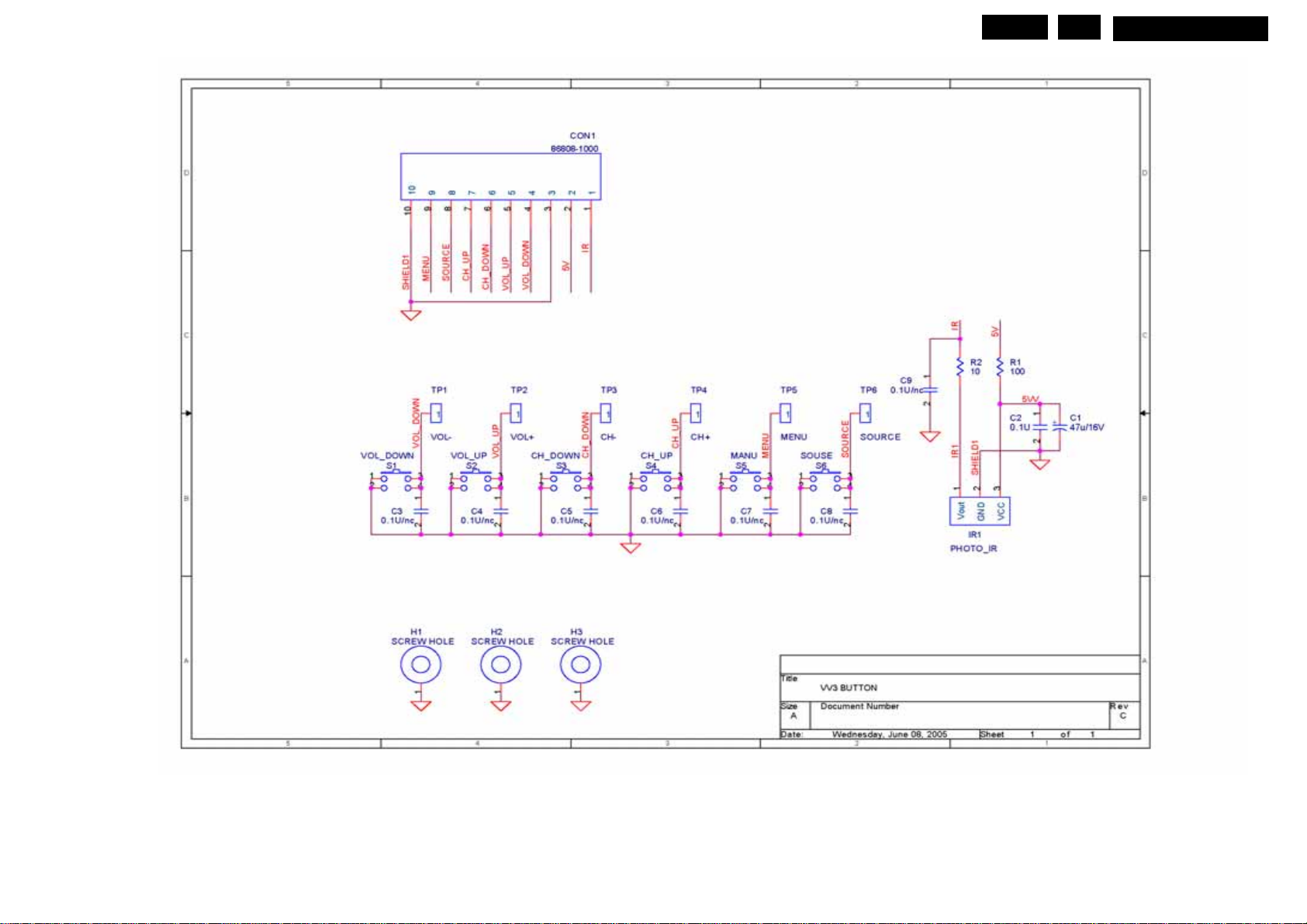
Button Board
Circuit Diagrams PCB Layouts
EN 38
7
MQC1.OA LA
Page 40
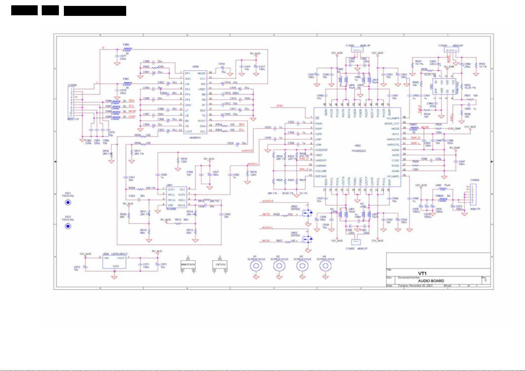
EN 39
Audio Board
7
MQC1.OA LA
Circuit Diagrams PCB Layouts
Page 41
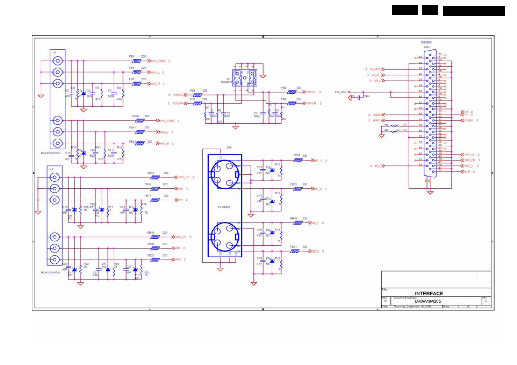
Tuner Board
Circuit Diagrams PCB Layouts
EN 40
7
MQC1.OA LA
Page 42
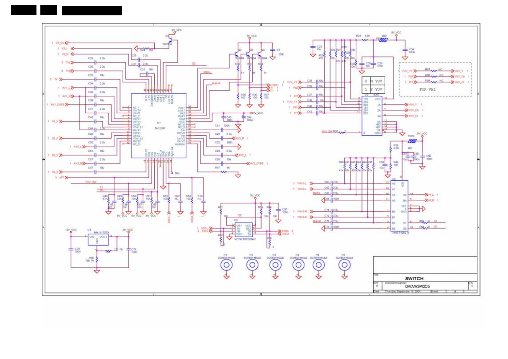
EN 41
7
MQC1.OA LA
Circuit Diagrams PCB Layouts
Page 43
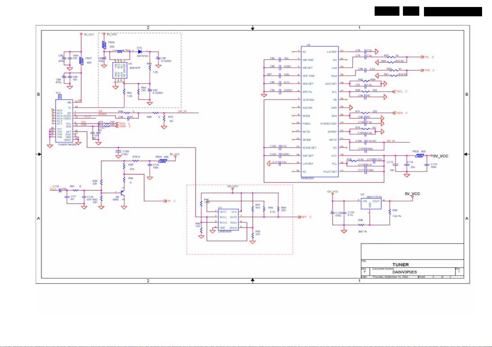
Circuit Diagrams PCB Layouts
EN 42
7
MQC1.OA LA
Page 44
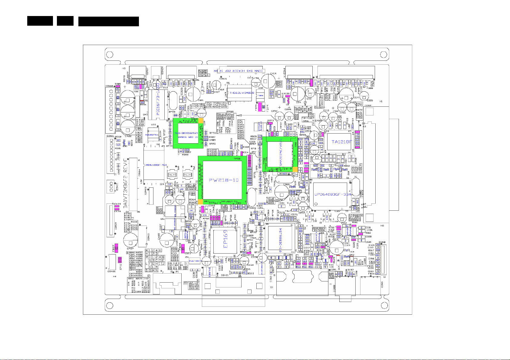
EN 43
7
Layout MB (Top side)
MQC1.OA LA
Circuit Diagrams PCB Layouts
Page 45
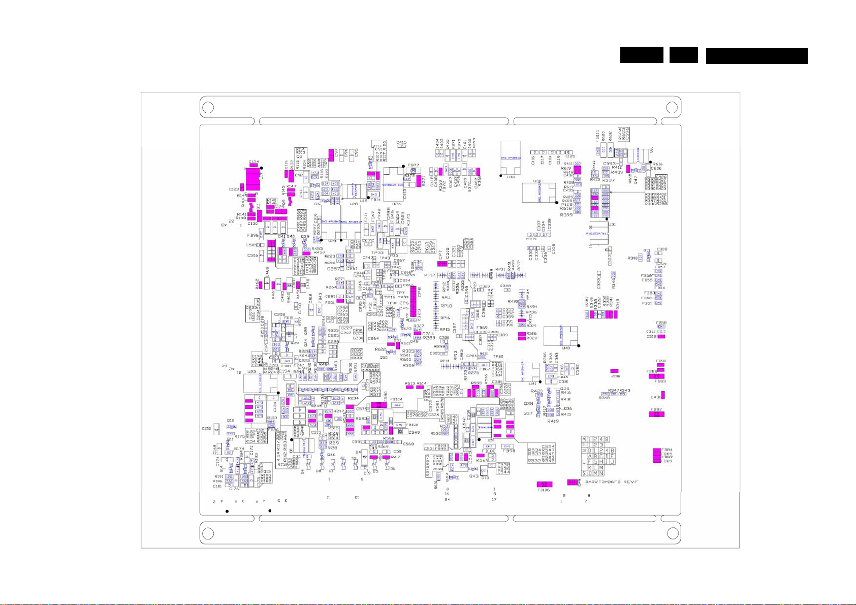
Layout MB (Bottom side)
MQC1.OA LA Block Diagrams 7EN 44
Page 46
Block Diagrams MQC1.OA LA
EN 45
7
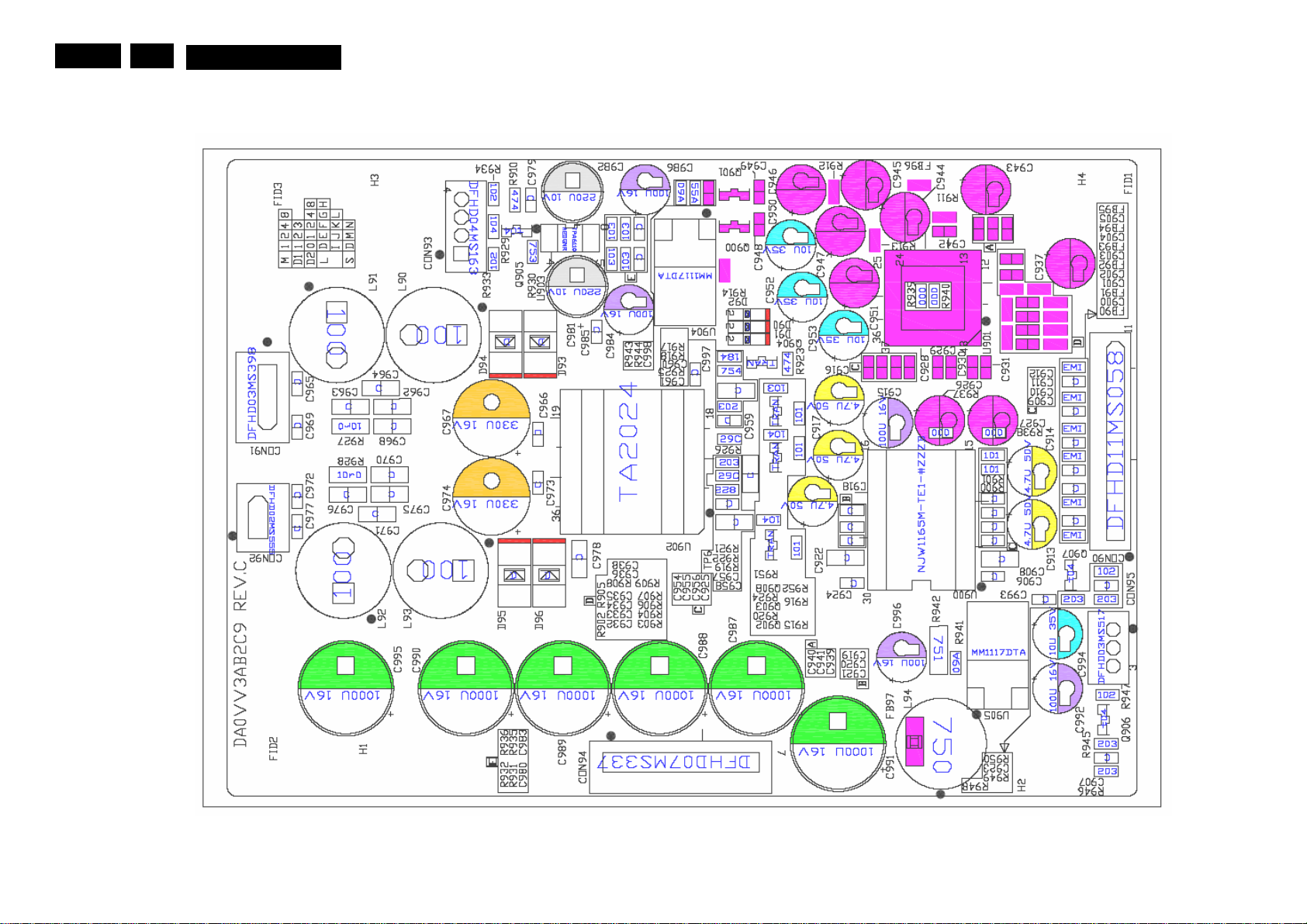
Layout Audio Board
Page 47
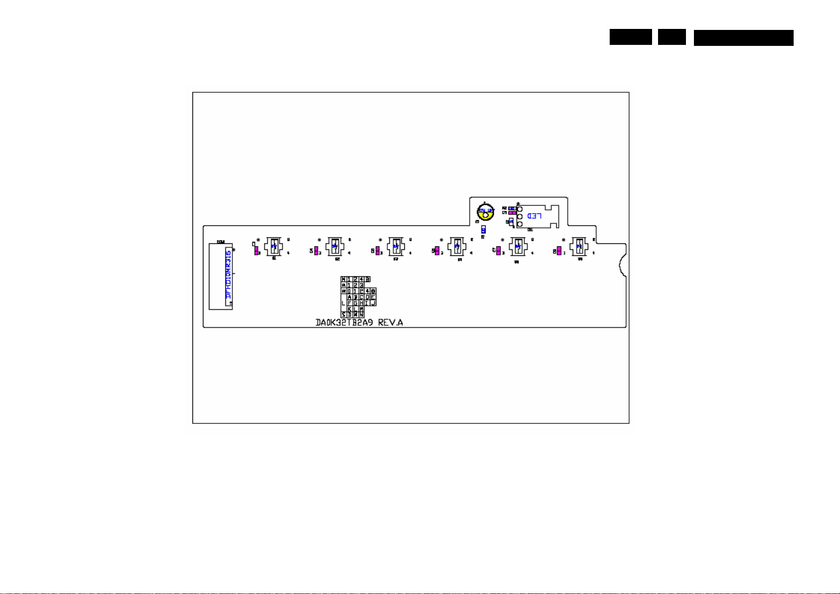
Layout Bottom Board (Top side)
Block Diagrams
EN 46
7
MQC1.OA LA
Page 48
Block Diagrams MQC1.OA LA
EN 47
7
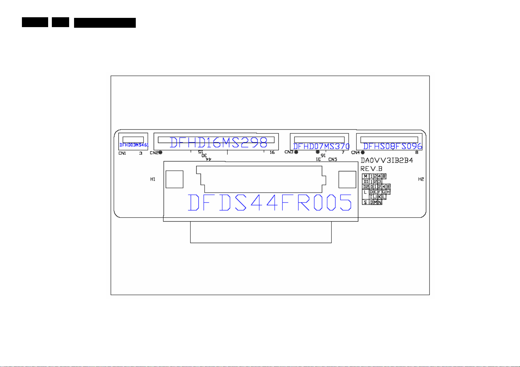
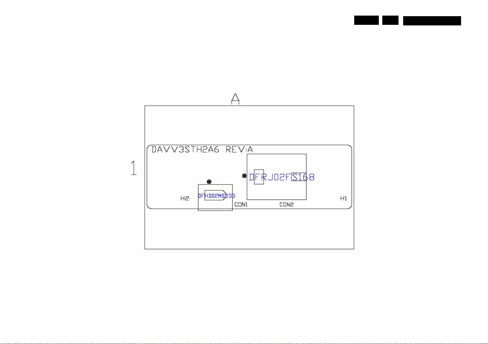
Layout Interface Board (Top side)
Page 49
Block Diagrams
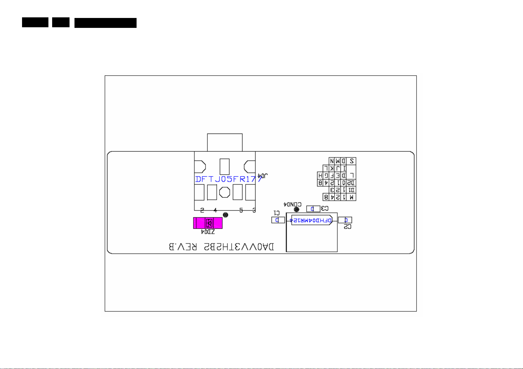
Layout speaker board (Top side)
EN 48
7
MQC1.OA LA
Page 50
Block Diagrams MQC1.OA LA
EN 49
7
Layout Earphone Board
Page 51
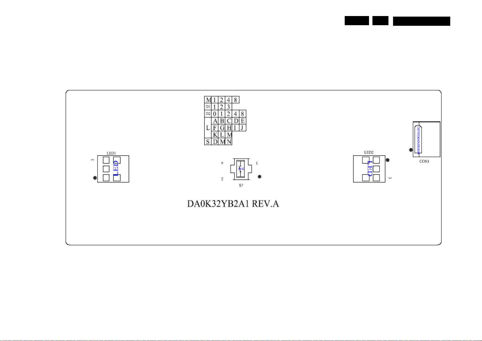
Layout Power Key Board
MQC1.OA LA Block Diagrams 7.EN 50
Page 52
EN 51
7
MQC1.OA LA
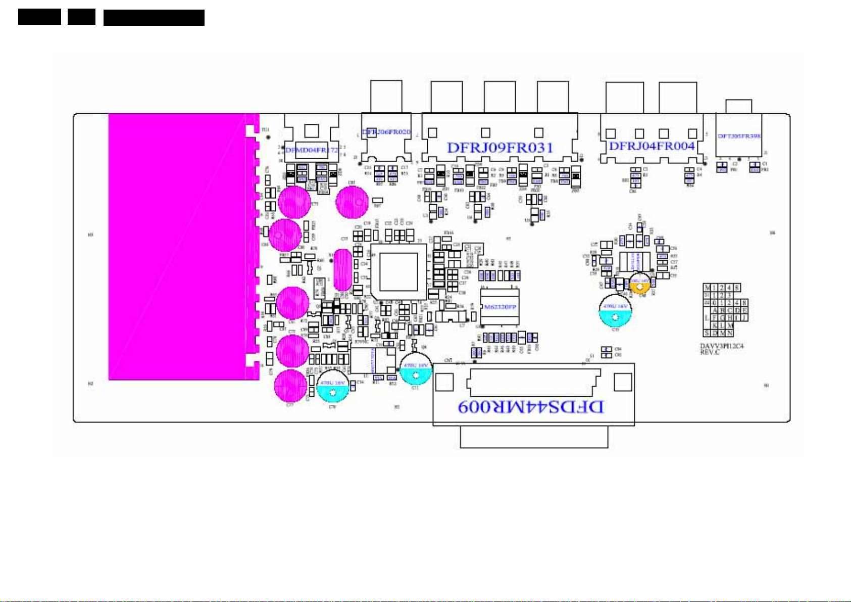
Layout Io Board
Circuit Diagrams PCB Layouts
Page 53
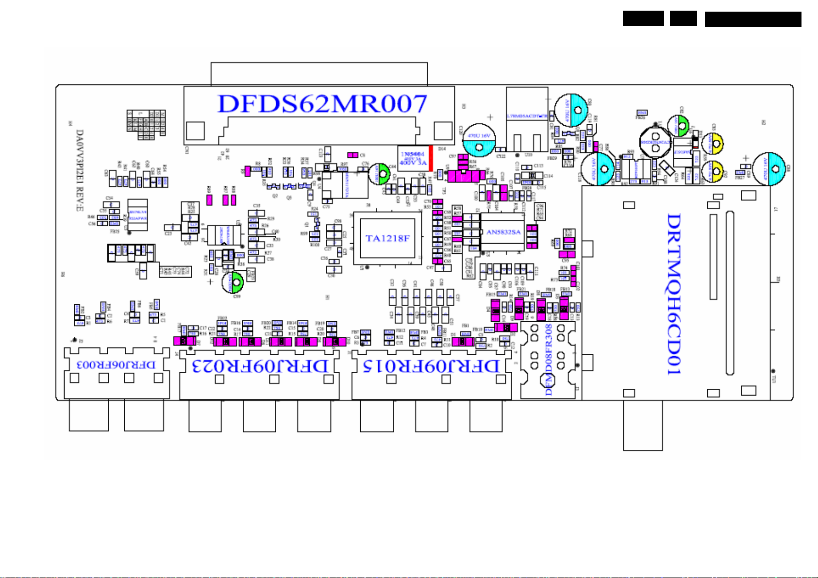
Layout Tuner Board
Circuit Diagrams PCB Layouts
EN52
7
MQC1.OA LA
Page 54
Alignments
EN 53
8.
MQC1.OA LA
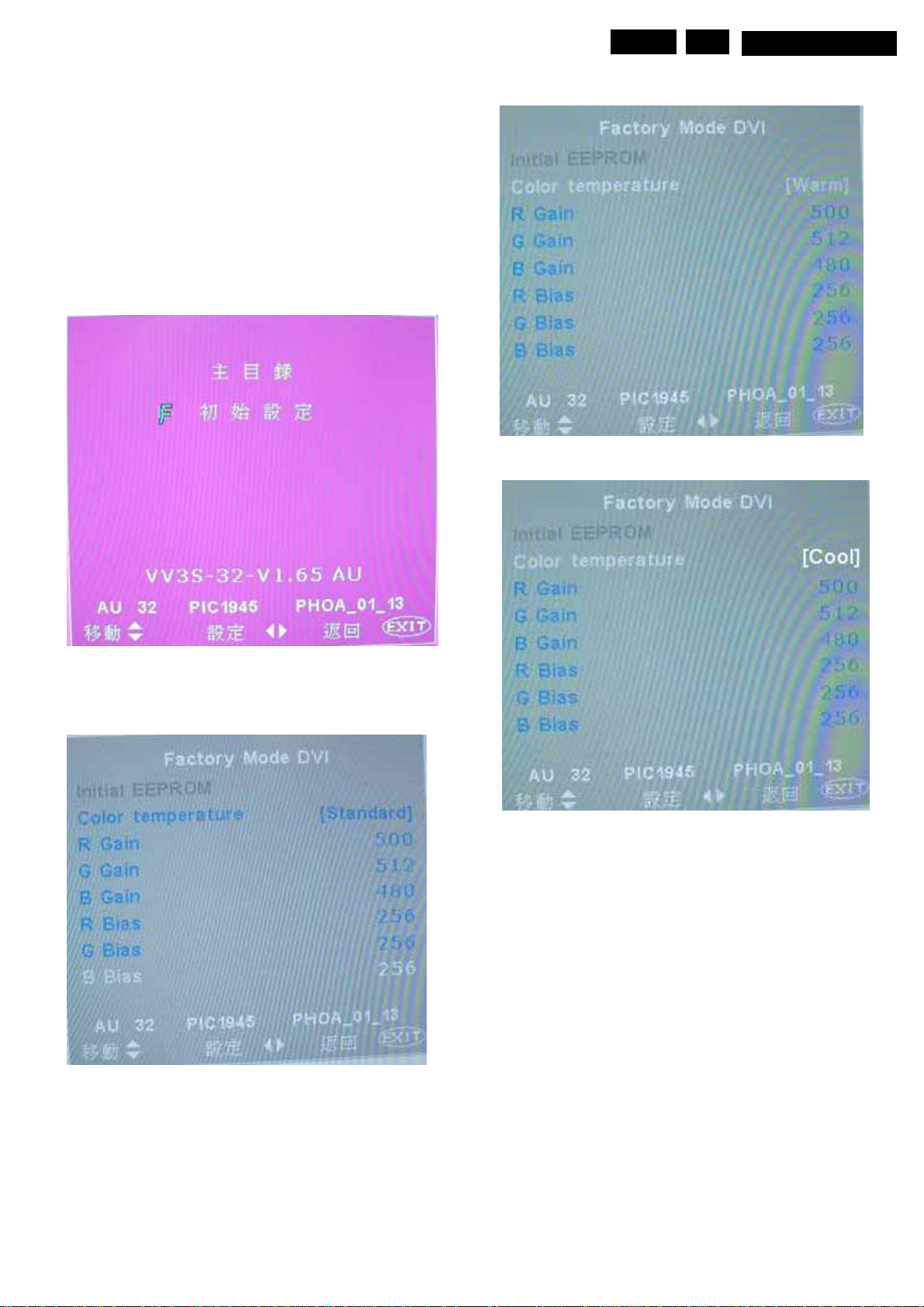
8. Alignments
White Balance
Purpose
. T o alignments color temperature
Tools
. Video Pattern Generator (Should be with DVI output)
. DVI cable
Setup
1. Connect DVI to TV set.
2. Enter Factory Mode (Hot-Key: Volume- & Channel+)
3. Switch color temperature mode.
Color temperature with 3 modes
Standard mode
Warm mode
Cool mode
4. Adjust R Gain, G Gain, B Gain
5. Adjust R Bain, G Bain, B Gain
Page 55

IC Data Sheet
EN 54
9.
9. IC Data Sheets EN 65
N/A
MQC1.OA LA
Page 56
Space Parts List
EN 55
10.
10. Space Parts List
MQC1.OA LA
TV set
40 996500035029 "VT3 M/B(FOR K32)TWN,PHILIPS"
31 996500035030 VV3 AUDIO BOARD ASSY
55 996500035034 VV3 INTERFACE/B ASSY
34 996500035035 PWR 180W(90~264VAC)
41 996500035036 CABLE ASSY HH2 MB-PWR
42 996500035037 CABLE ASSY K32 BUTTON
30 996500035038 CABLE ASSY VV3 MB-AUDIO
38 996500035039 CABLE ASSY VV3 EARPHONE
32 996500035040 CABLE ASSY VV3 AUDIO-PW
54 996500035041 CABLE ASSY VV3 SWITCH
57 996500035042 CABLE ASSY VV3 LIN OUT
56 996500035043 CABLE ASSY VV3 AV3
43 996500035044 CABLE ASSY VV3S SPK_R
37 996500035045 CABLE ASSY VV3S SPK_L
33 996500035046 CABLE ASSY VV3 INV CML
39 996500035047 CABLE ASSY VV3 LVDS CML
67 996500035048 CABLE ASSY K32 GND
29 996500035049 VV3 WALL MOUNT ASSY
68 996500035050 WIRE SADDLE CHA-4 VV3
69 996500035051 WIRE SADDLE MWS-7 VV3
46 996500035052 CHASSIS-M VV3
36 996500035053 CHASSIS-U CMO VV3
47 996500035054 CHASSIS-D CMO VV3
45 996500035055 CHASSIS-R CMO VV3
35 996500035056 CHASSIS-L CMO VV3
51 996500035057 D-SUB2 BRKT VV3
44 996500035058 INV SHIELD-QDI/CMO VV3
58 996500035059 IO NUT VT1
996500035060 SCREW M3*5-P-NI-+
996500035061 SCREW M4*6 P (NI)
996500035062 SCREW M3*4-I (NI)
996500035063 SCREW 4-40 UNC P-NI
70 996500035064 ID CARD-STN ZG1S)
13 996500035065 K32 BUTTON/B ASSY
12 996500035066 K32 LED/B ASSY
11 996500035067 VV3 EARPHONE BOARD ASSY
27 996500035068 VV3S SPEAKER/B ASSY
1 996500035069 K32 LCD BEZEL ASSY-PH
28 996500035070 PCB SPEAKER BKT VV3S
15 996500035071 VV3S BACK COVER SUB ASSY
20 996500035072 VV3 HINGE COVER ASSY
53 996500035073 BACK DOOR-R D1000
52 996500035074 BACK DOOR-L D1000
996500035075 SCREW T3*8-P(BLACK)
9 996500035076 K32 POWER-KEY ASSY
10 996500035077 KEY K32
6 996500035078 SPEAKER BOTTOM K32
7 996500035079 SPEAKER BRKT-L K32
8 996500035080 SPEAKER BRKT-R K3
17 996500035081 SCREW T4*12-B(BLACK)
14 996500035082 "LCD(TFT) 32"" V320B1-L01"
4 996500035083 SPEAKER VV3S FG-QT124-LLF
5 996500035084 SPEAKER VV3S FG-QT124-RLF
3 996500035085 K32 SPEAKER COVER-R ASSY
2 996500035086 K32 SPEAKER COVER-L ASSY
18 996500035087 FAN COVER D1000
71 996500035088 GASKET VV3
72 996500035089 "PANEL PROTECT FILM VV3,SAN"
50 996500035091 SCREW M4*15-B (NI+WAS+SPR)
19 996500035092 SCREW M3*8-B (BNI)
17 996500035081 SCREW T4*12-B(BLACK)
16 996500035094 SCREW T4*25-B(BNI)
48 996500035095 VV3 SWIVEL ASSY(SILVER)
49 996500035096 VV3 STAND BASE ASSY(SILVER)
Media Box
24 996500035101 VV3 I/O BOARD ASSY
22 996500035102 TUNER BOX TOP COVER VV3
25 996500035103 TUNER CHASSIS-NTSC AV4
23 996500035104 TUNER EMI SHIELD-NTSC
26 996500035105 SCREW T3*12 P (NI)
21 996500035106 SCREW M3*16 P(NI)
73 996500035107 TUNER EMI GASKET EU
66 996500035108 P300 PAD NTSC-3 VA1
65 996500035109 P300 PAD NTSC-6 VA1
61 996500035110 VV3 SUB IO/B ASSY
63 996500035102 TUNER BOX TOP COVER VV3
60 996500035111 TUNER2 CHASSIS VV3
62 996500035112 TUNER2 EMI SHIELDING VV3
74 996500035113 TUNER2 EMI SHIELD-2 VV3
59 996500035105 SCREW T3*12 P (NI)
64 996500035106 SCREW M3*16 P(NI)
996500035090 SCREW M4*10-B (BNI)
996500035093 SCREW 3 X 20.4-B (NI)
996500035097 POWER CORD SP-305+IS-14 BK
996500035098 CARTON CLASP VV3
996500035099 EPE SHEET VV3 SAY
996500035100 EPE BAG 1120*850(W)
996500035060 SCREW M3*5-P-NI-+
996500035114 SCREW T3*8 P (NI)
996500035063 SCREW 4-40 UNC P-NI
996500035114 SCREW T3*8 P (NI)
996500035063 SCREW 4-40 UNC P-NI
996500035060 SCREW M3*5-P-NI-+
996500035115 TUNER LABEL VV3SAYON
996500035116 I/O LABEL VV3 SAYON
996500035117 BUBBLE BAG(TUNER)VB1D
996500035118 CARTON(MB-PCBA) VA1
996500035119 PARTITION(TUNER ASSY)
996500035120 CARDBARD (470*432) VA1
996500035121 CARTON LABEL SK2+AMI
996500035122 ZIPPER BAG(#0) DK9
996500035123 CABLE ASSY VT1 ANT L2.5M
996500035124 CABLE ASSY VT1 RF L1.8M
996500035125 BATTERY LR03GW/2SK
996500035126 BATTERY LR03(SN)
996500035127 WARRANTY CARD(TW) K32
996500035128 MANUAL(TW) K32
996500035129 MEDIA CARTON(10 IN 1) VV3
996500035121 CARTON LABEL SK2+AMI
996500035130 BOX(MEDIA) VV3
Page 57

Revision list
11. Revision list
Manual xxxx xxx xxxx.0
• First release.
EN 56
11.
MQC1.OA LA
 Loading...