

Philips 2sd669a DATASHEETS
2SD669, 2SD669A
Silicon NPN Epitaxial
Application
Low frequency power amplifier complementary pair with 2SB649/A
Outline
TO-126 MOD
1. Emitter
2. Collector
1
2
3
3. Base
2SD669, 2SD669A
Absolute Maximum Ratings (Ta = 25°C)
Ratings
Item Symbol 2SD669 2SD669A Unit
Collector to base voltage V
Collector to emitter voltage V
Emitter to base voltage V
Collector current I
Collector peak current I
Collector power dissipation P
CBO
CEO
EBO
C
C(peak)
C
1
P
*
C
Junction temperature Tj 150 150 °C
Storage temperature Tstg –55 to +150 –55 to +150 °C
Note: 1. Value at TC = 25°C.
180 180 V
120 160 V
55V
1.5 1.5 A
33A
11W
20 20 W
2
2SD669, 2SD669A
Electrical Characteristics (Ta = 25°C)
2SD669 2SD669A
Item Symbol Min Typ Max Min Typ Max Unit Test conditions
Collector to base
breakdown voltage
Collector to emitter
breakdown voltage
Emitter to base
breakdown voltage
Collector cutoff current I
DC current transfer ratio h
Collector to emitter
saturation voltage
Base to emitter voltage V
Gain bandwidth product f
Collector output
capacitance
Notes: 1. The 2SD669 and 2SD669A are grouped by h
2. Pulse test.
V
(BR)CBO
V
(BR)CEO
V
(BR)EBO
CBO
FE1
h
FE2
V
CE(sat)
BE
T
180 — — 180 — — V IC = 1 mA, IE = 0
120 — — 160 — — V IC = 10 mA, RBE = ∞
5——5——VIE = 1 mA, IC = 0
——10——10µAVCB = 160 V, IE = 0
1
*
60 — 320 60 — 200 VCE = 5 V, IC = 150 mA*
30 — — 30 — — VCE = 5 V, IC = 500 mA*
——1 ——1 V IC = 500 mA,
I
= 50 mA*
B
— — 1.5 — — 1.5 V VCE = 5 V, IC = 150 mA*
— 140 — — 140 — MHz VCE = 5 V, IC = 150 mA*
2
Cob — 14 — — 14 — pF VCB = 10 V, IE = 0,
f = 1 MHz
as follows.
FE1
2
2
2
2
BCD
2SD669 60 to 120 100 to 200 160 to 320
2SD669A 60 to 120 100 to 200 —
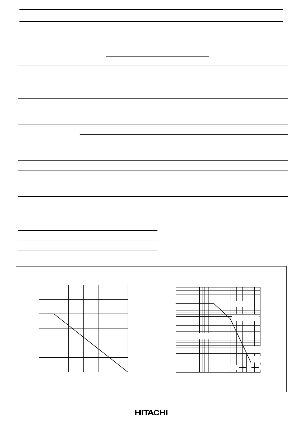
Maximum Collector Dissipation
30
(W)
C
20
10
Collector power dissipation P
0 50 100 150
Case temperature T
Curve
(°C)
C
Area of Safe Operation
3
1.0
(A)
C
0.3
DC Operation(TC = 25°C)
0.1
Collector current I
0.03
0.01
33010 3001 100
Collector to emitter voltage V
(13.3 V, 1.5 A)
(40 V, 0.5 A)
2SD669
CE
(120 V, 0.04 A)
(160 V, 0.02A)
2SD669A
(V)
3
 Loading...