

Page 1

27ƎLCD Color Monitor Chassis: Meridian 3
Service
Service
Service
Description
Page
Table of Contents.........................................………….1
Revision List………….................................................2
Important Safety Notice…………................................3
1. Monitor Specifications….........................................5
2. LCD Monitor Description….....................................7
3. Operation Instructions….........................................8
3.1General Instructions…………………………….…...8
3.2 Control Buttons…………..…………………….…8
3.3 OSD Menu………………….................................9
4. Input/output Specification............................……10
4.1 Input Signal Connector.................................……10
4.2 Resolution & Preset Modes.................................11
4.3 Pixel Defect Policy…………………………………13
4.4 Failure Mode of Panel………………………….....15
5. Block Diagram………………………….................16
5.1 Scaler Board....................................………….....16
5.2 Power Board........................... ......…...........17
6. Schematic Diagram.............................................. 18
Description
Page
6.1 Scaler Board…………………….…………………18
6.2 Power Board.................................................…...23
6.3 Key Board…….…………………………………25
7. PCB Layout………………………………………...26
7.1 Scaler Board……………………………………..26
7.2 Power Board……………...………………………27
7.3 Key Board…….……………………………………28
8. Wiring Diagram………………………………….…..29
9. Scaler Board Overview…………………………....30
10. Mechanical Instructions………………………....31
1 1. Repair Flow Chart…….……………………………33
12. ISP Instructions...…............................................37
13. DDC Instructions….............................................45
14. White Balance, Luminance Adjustment…...........55
15. Monitor Exploded View…....................................57
16. Recommended & Spare Parts List...….............58
17. General Product Specification………….……….66
SAFETY NOTICE
ANY PERSON ATTEMPTING TO SERVICE THIS CHASSIS MUST FAMILIARIZE HIMSELF WITH THE
CHASSIS AND BE AWARE OF THE NECESSARY SAFETY PRECAUTIONS TO BE USED WHE N
SERVICING ELECTRONIC EQUIPMENT CONTAINING HIGH VOLTAGES.
CAUTION: USE A SEPARATE ISOLATION TRANSFOMER FOR THIS UNIT WHEN SERVICING
REFER TO BACK COVER FOR IMPORTANT SAFETY GUIDELINES
Copyright 2012 Philips Consumer Lifestyle Subject to modification ƻK Aug.14, 2012
273E3LSW/93
Page 2

!
!
Meridian 3
2
Revision List
Version Release Date Revision History
A00 Aug.14, 2012 Initial release, Draft Version
Page 3

3
Meridian 3
Important Safety Notice
This electronic user guide is intended for anyone who uses the Philips monitor. Take time to read this user manual
before you use your monitor. It contains important information and notes regarding operating your monitor. The
Philips guarantee applies provided the product is handled properly for its intended use, in accordance with its
operating instructions and upon presentation of the o riginal invoice or cash receipt, indicatin g the date of p urchase,
dealers name and model and production number of the product.
Warnings
Use of controls, adjustments or procedures other than those specified in this document ation may result in exposure
to shock, electrical hazards and/or mechanical hazards. Read and follow these instructions when connecting and
using your computer monitor.
Operation
y Keep the monitor out of direct sunlight and away from stoves or any other heat source.
y Remove any object that could fall into ventilation holes or prevent proper cooling of the monitor’s electronics.
y Do not block the ventilation holes on the cabinet.
y When positioning the monitor , make sure the power plug and outlet are easily accessible.
y If turning off the monitor by detaching the power cable or DC power cord, wait for 6 seconds before attaching
the power cable or DC power cord for normal operation.
y Please use approved power cord provided by Philips all the time. If your power cord is missing, please contact
with your local service center. (Please refer to Customer Care Consumer Information Center)
y • Do not subject the monitor to severe vibration or high impact conditions during operation.
y • Do not knock or drop the monitor during operation or transportation.
Maintenance
y To protect your monitor from possible damage, do not put excessive pressure on the LCD panel. When moving
your monitor, grasp the frame to lift; do not lift the monitor by placing your hand or fingers on the LCD panel.
y Unplug the monitor if you are not going to use it for an extensive period of time.
y Unplug the monitor if you need to clean it with a slightly damp cloth. The screen may be wiped with a dry cloth
when the power is off. However , never use organic sol vent, such as, alcoh ol, or ammonia-ba sed liquids to clean
your monitor.
y To avoid the risk of shock or permanent damage to the set, do not expose the monitor to dust, rain, water, or
excessive moisture environment.
y If your monitor gets wet, wipe it with dry cloth as soon as possible.
y If foreign substance or water gets in your monitor, please turn the power off immediately and disconnect the
power cord. Then, remove the foreign substance or water, and send it to the maintenance center.
y Do not store or use the monitor in locations exposed to heat, direct sunlight or extreme cold.
y In order to maintain the best performance of your monitor and use it for a longer lifetime, please use the monitor
in a location that falls within the following temperature and humidity ranges.
¾ Temperature: 0-40°C 32-95°F
¾ Humidity: 20-80% RH
Page 4

!
!
Meridian 3
4
y IMPORTANT: Always activate a moving screen saver program when you leave your monitor unattended.
Always activate a periodic screen refresh application if your monitor will display unchanging static content.
Uninterrupted display of still or static images over an extended period may cause “burn in”, also known a s
“after-imaging” or “ghost imaging”, on your screen. “Burn-in”, “after-imaging”, or “ghost imaging” is a
well-known phenomenon in LCD panel technology. In most cases, the “burned in” or “after-imaging” or “ghost
imaging” will disappear gradually over a period of time after the power has bee n switched off.
Warning
Severe” burn-in” or “after-image” or “ghost image” symptoms will not disappear and cannot be repaired. The
damage mentioned above is not covered under your warranty.
Service
y The casing cover should be opened only by qualified service personnel.
y If there is any need for any document for repair or integration, please contact with your local service center.
(Please refer to the chapter of “Consumer Information Center”)
y For transportation information, please refer to “Technical Specifications”.
y Do not leave your monitor in a car/trunk under direct sun light.
Note
Consult a service technician if the monitor does not operate normally, or you are not sure what procedure to take
when the operating instructions given in this manual have been followed.
Page 5
5
Meridian 3
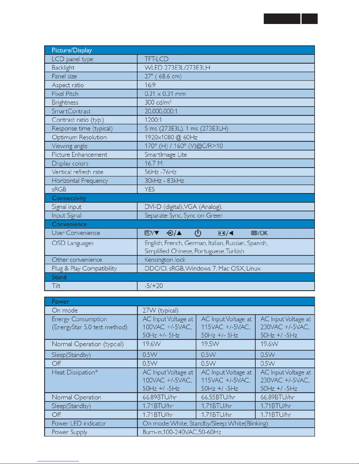
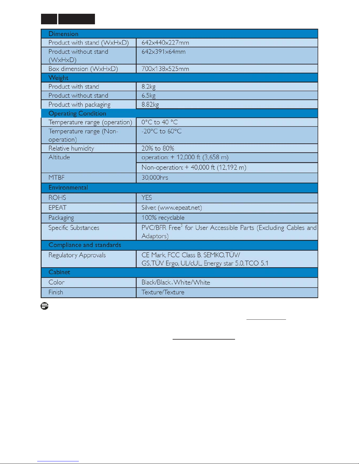
1. Monitor Specifications
Technical specifications
Page 6
!
!
Meridian 3
6
Note:
1. EPEAT Gold or Silver is valid only where Philips registers the product Please visit www. epeat.net
for
registration status in your country.
2. This data is subject to change without notice. Go to www.philips.com/support
to download the latest version of
leaflet.
3. This monitor is brominated flame retardant and polyvinyl chloride-free (PVC/BFR free) for all user accessible
parts (excluding cables and adaptors). Organob romine compounds in the form of flame retardants must not be
used in those portions equal to or greater than 0.09%(900ppm maximum of Bromine) and organobromine
compounds in the form of polyvinyl chloride or polyvinyl chloride congeners must not be used in those portions
equal to or greater than 0.1% (1000ppm maximum of Chlorine).
Page 7
7
Meridian 3
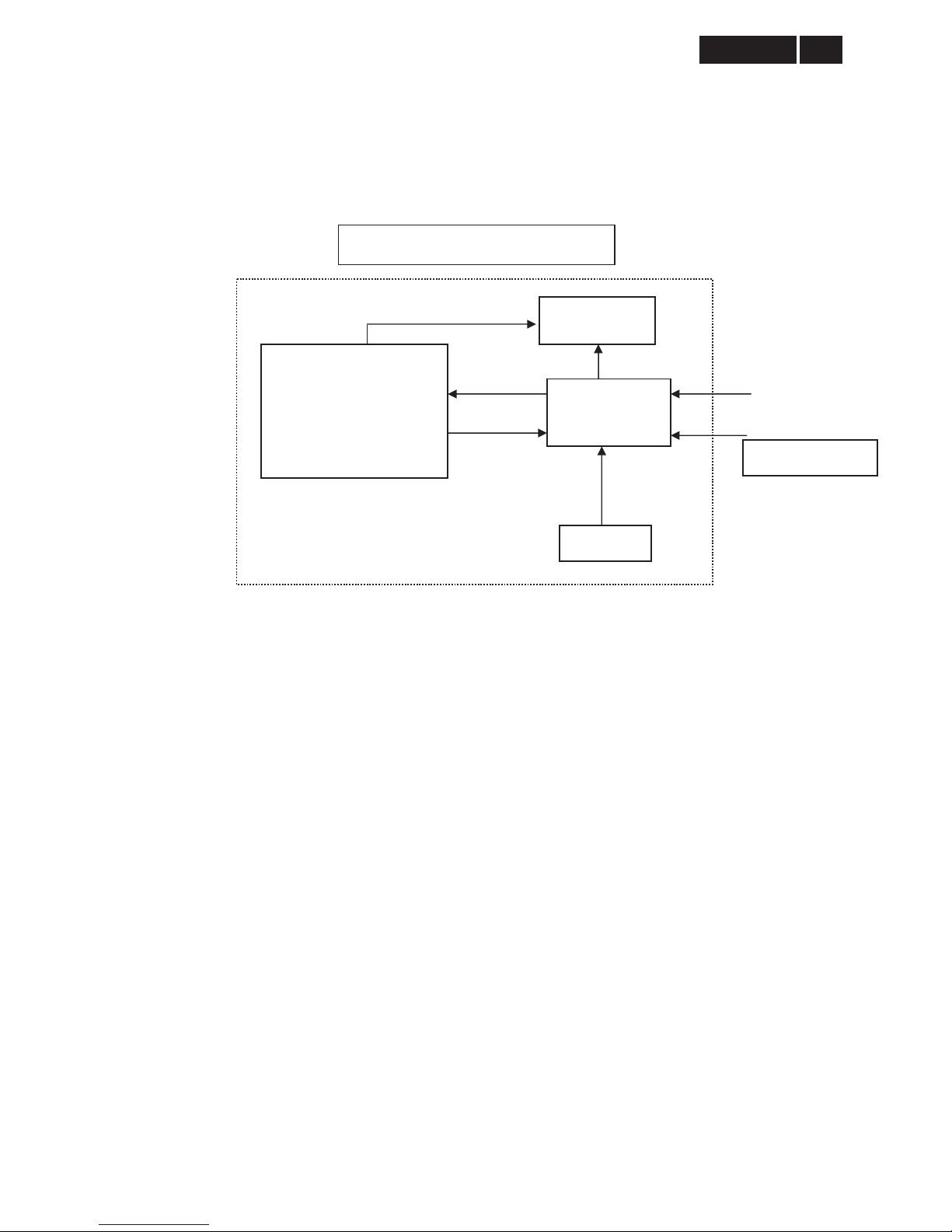
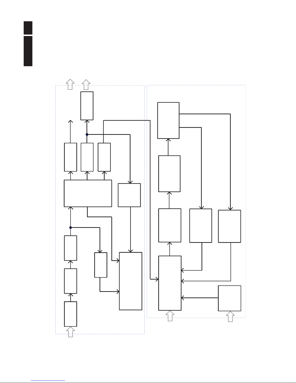
2. LCD Monitor Description
The LCD monitor will contain a scaler board, a power board and a key board. The scaler board houses the flat
panel control logic, brightness control logic and DDC.
The power board will provide AC to DC inverter voltage to drive the backlight of panel and the scaler board chips
each voltage.
Monitor Block Diagram
LED Panel
Scaler Board
LED Drive
Key Board
Video signal, DDC
HOST Computer
AC IN
100 ~ 240 V
Power Board
Page 8
!
!
Meridian 3
8
3. Operating Instructions
3.1 General Instructions
Press the power button to turn the monitor on or off.
The other control knobs are located at front panel of
the monitor. By changing these setting, the picture
can be adjusted to your personal preference.
γThe power cord should be connected.
γ Press the power button to turn on the monitor.
The power indicator will light up.
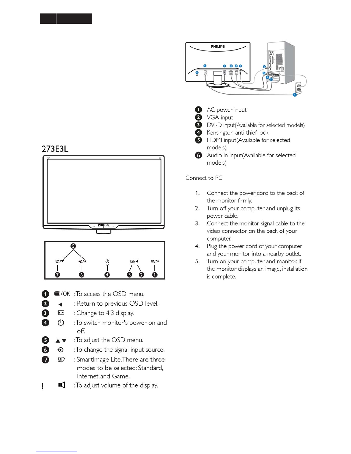
3.2 Control Buttons
Operating the Monitor
Connecting to your PC
Page 9
9
Meridian 3
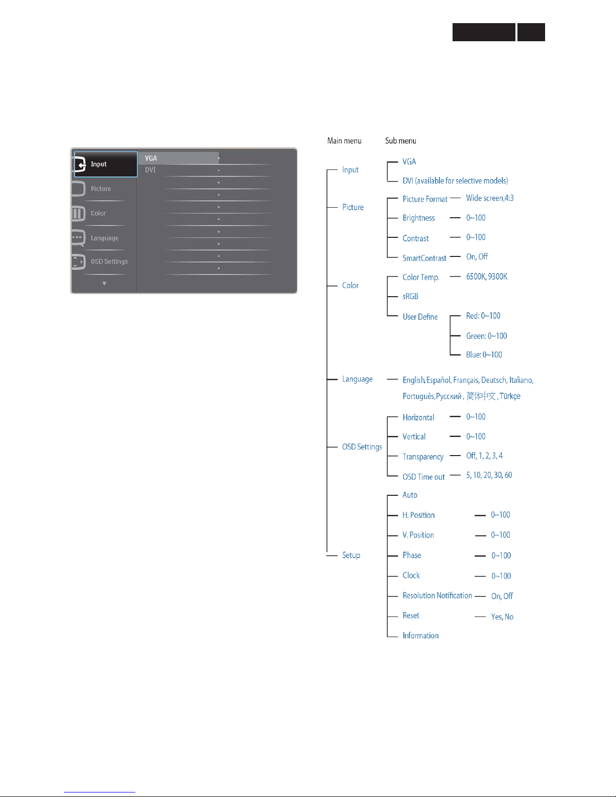
3.3 OSD Menu
On-Screen Display (OSD) is a feature in all Philips
LCD monitors. It allows an end user to adjust screen
performance or select functions of the monitors directly
through an on-screen instruction window. A user
friendly on screen display interface is shown as below:
Basic and simple instruction on the control keys
In the OSD shown above users can pressźŸ buttons
at the front bezel of the monitor to move the cursor,
and press OK button to confirm the choice or change.
The OSD Menu
Below is an overall view of the structure of the
On-Screen Display. You can use this as a reference
when you want to work your way around the different
adjustments later on.
Page 10
!
!
Meridian 3
10
4. Input/ Output Specification
4.1 Input Signal Connector
D-sub Connector
Pin No. Signal Name
1 Red
2 Green/ SOG
3 Blue
4 Sense (GND)
5 Cable Detect (GND)
6 Red GND
7 Green GND
8 Blue GND
9 DDC +3.3V or +5V
10 Logic GND
11 Sense (GND)
12 Bi-directional data
13 H/H+V sync
14 V-sync
15 Data clock
DVI Connector
Pin No. Description
1 T.M.D.S. data22 T.M.D.S. data2+
3 T.M.D.S. data2 shield
4 No Connect
5 No Connect
6 DDC clock
7 DDC data
8 No Connect
9 T.M.D.S. data110 T.M.D.S. data1+
11 T.M.D.S. data1 shield
12 No Connect
13 No Connect
14 +5V Power
15 Ground (for +5V)
16 Hot plug detect
17 T.M.D.S. data018 T.M.D.S. data0+
19 T.M.D.S. data0 shield
20 No Connect
21 No Connect
22 T.M.D.S clock shield
23 T.M.D.S. clock+
24 T.M.D.S. clock-
Page 11
11
Meridian 3
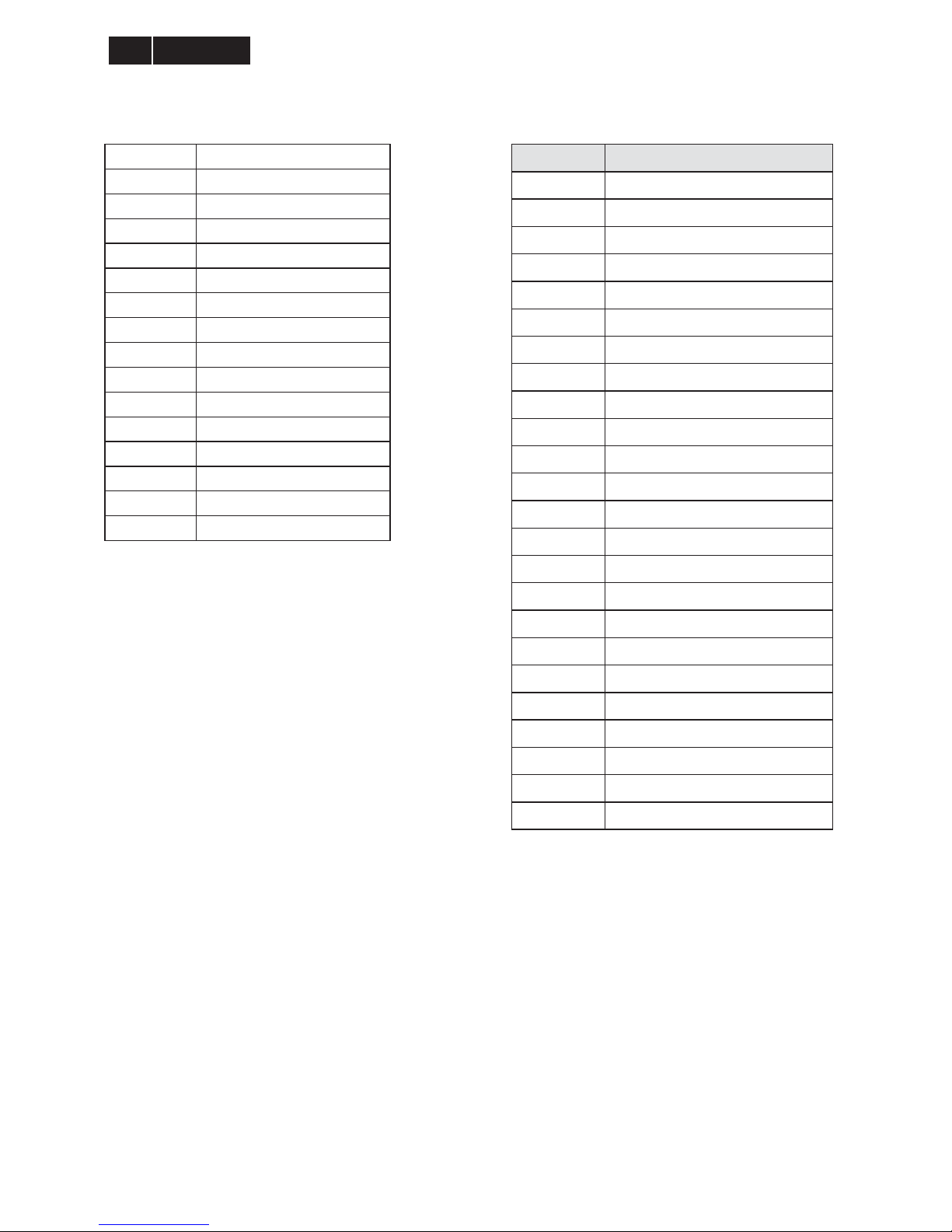
4.2 Resolution & Preset Modes
Maximum Resolution
1920 x 1080 at 60 Hz (analog input)
1920 x 1080 at 60 Hz (digital input)
Recommended Resolution
1920 x 1080 at 60 Hz (digital input)
Power Management Definition
If you have VESA DPM compliance disp lay card or software installed in your PC, the monitor can automatically
reduce its power consumption when not in use. If an input from a keyboard, mouse or other input device is detected,
the monitor will 'wake up' automatically. The following table shows the power consumption and signaling of this
automatic power saving feature:
Page 12

!
!
Meridian 3
12
The following setup is used to measure power consumption on this monitor.
·Native resolution:1920×1080
·Contrast: 50%
·Brightness: 300 nits
·Color temperature:6500k with full white pattern
Note:
This data is subject to change without notice.
Page 13
13
Meridian 3
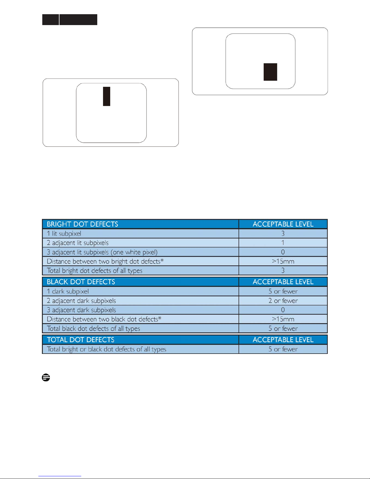
4.3 Pixel Defect Policy
Philips strives to deliver the highest quality products.
We use some of the industry's most advanced
manufacturing processes and practice stringent quality
control. However, pixel or sub pixel defects on the TFT
LCD panels used in flat panel monitors are sometimes
unavoidable. No manufacturer can guarantee that all
panels will be free from pixel defects, but Philips
guarantees that any monitor with an unacceptable
number of defects will be repaired or replaced under
warranty. This notice explains the different types of
pixel defects and defines acceptable defect levels for
each type. In order to qualify for repair or replacement
under warranty, the number of pixel defects on a TFT
LCD panel must exceed these acceptable levels. For
example, no more than 0.0004% of the sub pixels on a
monitor may be defective. Furthermore, Philips sets
even higher quality standards for certain types or
combinations of pixel defects that are more noticeable
than others. This policy is valid worldwide.
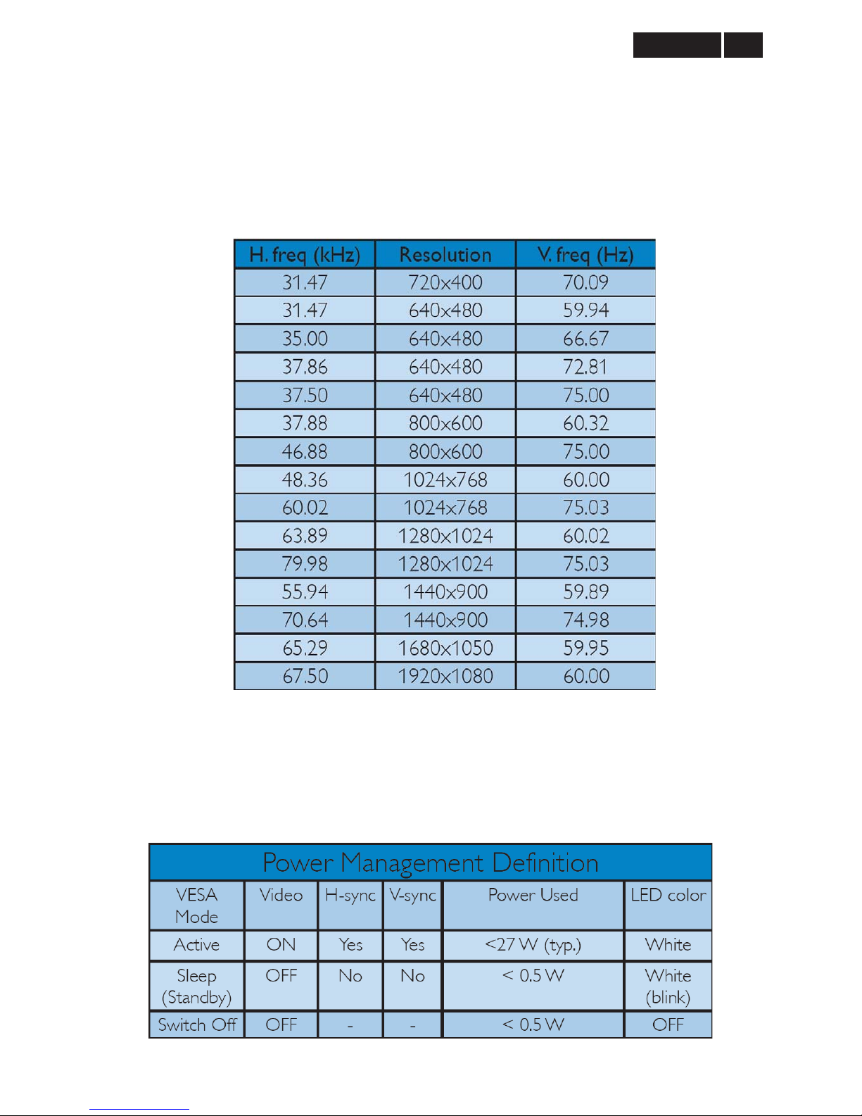
Pixels and Sub pixels
A pixel, or picture element, is composed of three sub
pixels in the primary colors of red, green and blue.
Many pixels together form an image. When all sub
pixels of a pixel are lit, the three colored sub pixels
together appear as a single white pixel. When all are
dark, the three colored sub pixels together appear as a
single black pixel. Other combinations of lit and dark
sub pixels appear as single pixels of other colors.
Types of Pixel Defects
Pixel and sub pixel defects appear on the screen in
different ways. There are two categories of pixel
defects and several types of sub pixel defects within
each category.
Bright Dot Defects
Bright dot defects appear as pixels or sub pixels that
are always lit or 'on'. That is, a bright dot is a sub-pixel
that stands out on the screen when the monitor
displays a dark pattern. There are the types of bright
dot defects.
One lit red, green or blue sub pixel
Two adjacent lit sub pixels:
- Red + Blue = Purple
- Red + Green = Yellow
- Green + Blue = Cyan (Light Blue)
Three adjacent lit sub pixels (one white pixel)
Note:
A red or blue bright dot must be more than 50 percent
brighter than neighboring dots while a green bright dot
is 30 percent brighter than neighboring dots.
Page 14
!
!
Meridian 3
14
Black Dot Defects Black dot defects appear as pixels
or sub pixels that are always dark or ‘off’. That is, a
dark dot is a sub-pixel that stands out on the screen
when the monitor displays a light pattern. There are
two types of black dot defects:
Proximity of Pixel Defects
Because pixel and sub pixels defects of the same type
that are near to one another may be more noticeable,
Philips also specifies tolerances for the proximity of
pixel defects.
Pixel Defect Tolerances
In order to qualify for repair or replacement due to pixel
defects during the warranty period, a TFT Monitor
panel in a Philips flat panel monitor must have pixel or
sub pixel defects exceeding the tolerances listed in the
following tables.
Note:
1. 1 or 2 adjacent sub pixel defects = 1 dot defect
2. This monitor is ISO 9241-307 compliant.( ISO9241-307 : Ergonomic requi rement, analysis and compliance test
methods for electronic visual displays)
Page 15
15
Meridian 2
4.4 Failure Mode Of Panel
Failure description
Phenomenon
Vertical block defect
Vertical dim lines
Vertical lines defect
(Always bri
g
ht or dark)
Horizontal block defect
Horizontal dim lines
Horizontal lines defect
(Always bri
g
ht or dark)
Has bri
g
ht or dark pixel
Polarizer has bubbles
Polarizer has bubbles
Foreign material inside
polarizer. It shows liner or
dot shape.
Concentric circle formed
Bottom back light of LCD is
brighter than normal
Back light un-uniformity
Backli
g
ht has foreign material.
Black or white color, liner or
circular type
Quick reference for failure mode of LCD panel
this pa
g
e presents problems that could be made by LCD panel.
It is not necessary to repair circuit board. Simply follow the mechanical
instruction on this manual to eliminate failure by replace LCD panel.
Page 16
!
!
Meridian 3
16
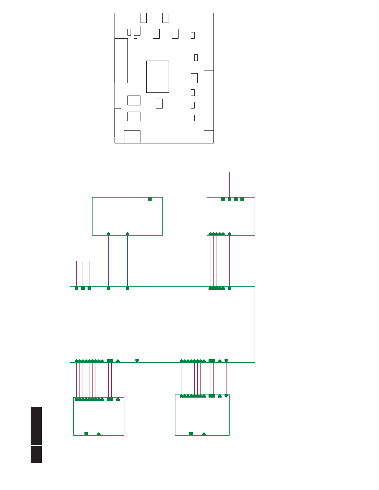
5. Block Diagram
5.1 Scaler Board
PB[0..9]
03.D VI I N PU T
03.D VI I N PU T
RX0+
RX0-
RX1-
RX1+
RX2+
RX2-
RXC-
RXC+
DDCSCL2
DDCSDA2
DVI_CABLE_DET
EDID_WP
+5V
DVI_HPD
Adj_BACKLIGHT
on_BACKLIGHT
Audio_EN
Audio_DET
PS_EN
Panel_ON
+5V
VCC3.3
VCC1.8
VLCD
VLCD
R0+
R0-
SOG_DET
G0+
G0-
B0+
B0-
AHS0
AVS0
DDCSCL1
DDCSDA1
EDID_WP
VGA_CABLE_DET
PA[0..9]
+5V
EDID_WP
RX0+
RX1-
RX0-
RXC-
RX2+
RX2-
RXC+
RX1+
DDCSCL2
DDCSDA2
DVI_CABLE_DET
+5V
EDID_WP
DVI_HPD
VCC3.3
VCC1.8
+5V
PLACEMENT
U401U402
U106U107
U402U401 U703U701
CN701
U102
U103
U105U104
U101
Q706
Q705
Q704
U403
CN406
CN407
CN408
CN409
CN102 CN101
02.INPUT
02.D-SUB I N PU T
R0+
R0-
SOG_DET
G0+
G0-
B0+
B0-
+5V
AHS0
AVS0
DDCSCL1
DDCSDA1
EDID_WP
VGA_CABLE_DET
04.SCALER
04.SCALER
Adj_BACKLIGHT
on_BACKLIGHT
Audio_EN
Audio_DET
PS_EN
Panel_ON
PB[0..9]
PA[0..9]
R0+
R0-
SOG_DET
G0+
G0-
B0+
B0-
AHS0
AVS0
DDCSCL1
DDCSDA1
EDID_WP
VGA_CABLE_DET
RXC+
RXC-
RX2-
RX2+
RX1+
RX1-
RX0-
RX0+
DDCSCL2
DDCSDA2
DVI_CABLE_DET
DVI_HPD
VCC1.8
VCC3.3
+5V 05.PANEL INTERFACE
05.PANEL INTERFACE
VLCD
PA[0..9]
PB[0..9]
06.POWER
06.POWER
Adj_BACKLIGHT
on_BACKLIGHT
Audio_EN
Audio_DET
PS_EN
Panel_ON
+5V
VCC3.3
VCC1.8
VLCD
Page 17
17
Meridian 3
5.2 Power Board
MITSUBISHI 27W
POWER BO ARD BL O CK DIAGRAM
EMI Filter
Circuit
Input AC Source
85v / 60 Hz ~
264v / 50 Hz
Inrush
Prevention
Rectification
Main
Transformer
Switching Circuit
( PWM Control IC
& MOSFET )
Rectification
Feedback
Control
Circuit
B+
Diode Rectifier
and Filter Circuit
Output (+5V) To Main board /Audio *2W
Fuse For OLP
Diode Rectifier
and Filter Circuit
Output (+16V) To
USB(Option) Circuit
Diode Rectifier
and Filter Circuit
PWM Control C ircuit
( PWM Control IC _O2_TA9687 )
DC To AC
Transformer
( EEL-19 * 1 pcs )
Driver Circuit
( Full Bridge )
CCFL Lamp * 4 pcs
Abnormal Protect
Control Circuit
Feedback Control
Circuit
Dimming
Control
Circuit
ON / OFF Control Signal
( 5v: on / 0v:off )
Dimming Control Signal
(Burst model Signal )
Adapter Block Circuit
Inverter Block Ci rcuit
Page 18
!
18
Meridian 3
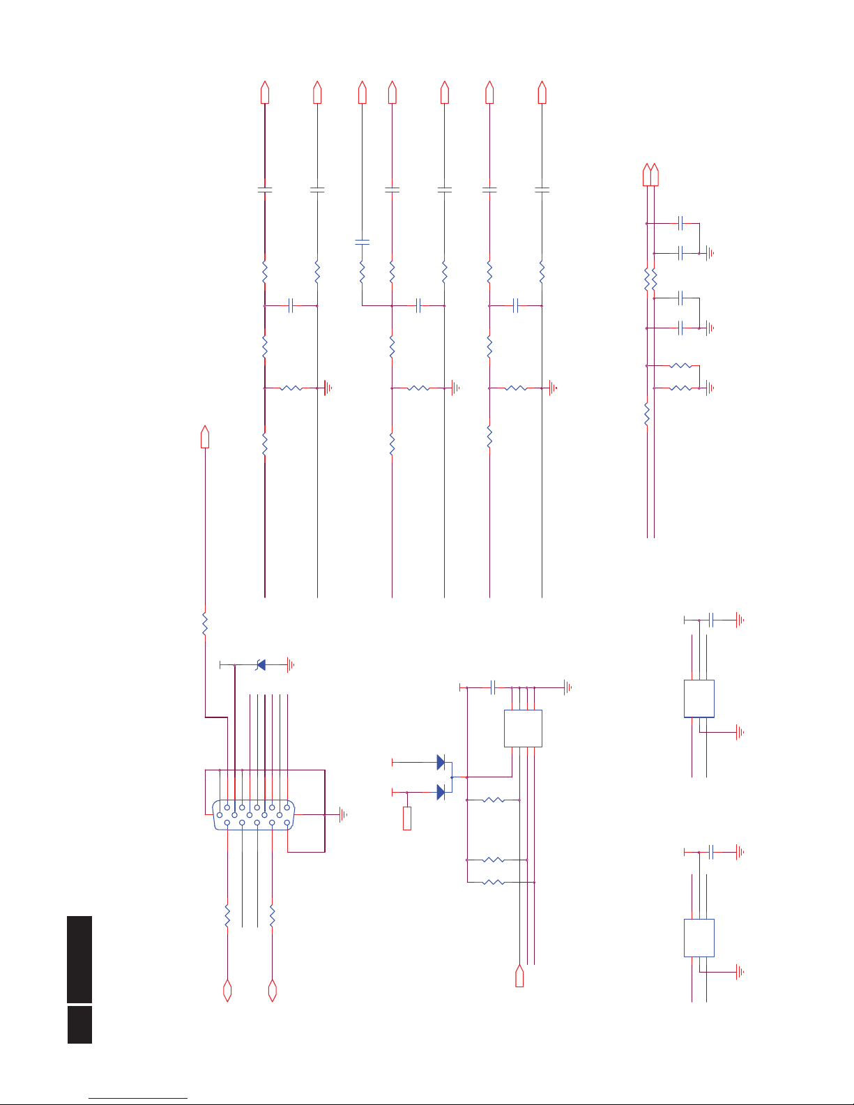
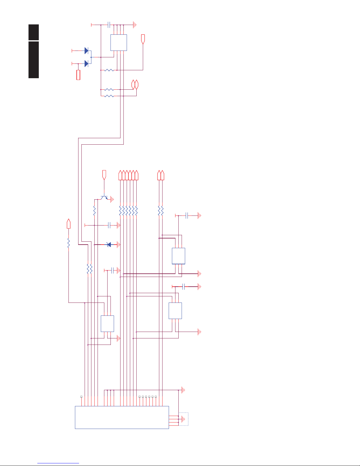
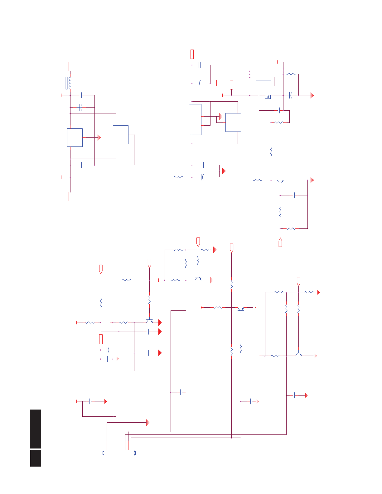
6. Schematic
6.1 Scaler Board (715G3737M02000004K)
Remark: Parts position can be searched by using FIND function in PDF.
BIN0-
BIN0
GIN0HSIN0
VSIN0 DDCSDA_A
DDCSCL_A
BIN0
DET_VGA
C182
22P 50V
C181
22P 50V
EDID_WP
GIN0
RIN0-
GIN0-
BIN0-
RIN0
RIN0
R121
100R 1/16W 5%
C112
NC/ 22pF 50V
R120
75R 1/16W 1%
C104
47N16V
RIN0
R119
100R 1/16W 5%
R113
100R 1/16W 5%
U101
CAT24C02WI-GT3
A01A12A2
3
VSS
4
SDA5SCL6WP7VCC
8
C108
47N16V
R123 100R 1/16W 5%
R111
100R 1/16W 5%
R124 100R 1/16W 5%
U103
AZC399-04S
I/O11GND2I/O2
3
I/O3
4
VDD
5
I/O4
6
R122 0R05 1/10W
C114
100NF 25V
R104
0R05 1/16W
C111
NC/ 22pF 50V
R114 4K7 1/16W 5%
C110
47N16V
BIN0
C107
47N16V
R115 4K7 1/16W 5%
CN101
DB15
162738495
11
12
13
14
15
10
17 16
R112
75R 1/16W 1%
D101
BAV70
3
1
2
R109
0R05 1/16W
C105 47N16V
R101
100R 1/ 16W 5%
R102 100R 1/16W 5%
R126
2K2 1/16W 5%
C113
100NF 25V
R106
100R 1/ 16W 5%
R103
0R05 1/16W
C109
5PF 50V
R116 22K 1/16W 5%
R110
0R05 1/16W
R108
100R 1/16W 5%
R125
2K2 1/16W 5%
C102
47N16V
R107
75R 1/16W 1%
R117
0R05 1/16W
ZD101
RLZ5.6B
C101
220N16V
R105
100R 1/16W 5%
R118
0R05 1/16W
U102
AZC399-04S
I/O11GND2I/O2
3
I/O3
4
VDD
5
I/O4
6
C106
5PF 50V
C103
5PF 50V
B0- 5
R0+ 5
B0+ 5
G0- 5
R0- 5
G0+ 5
AVS0 5
AHS0 5
SOG_DET 5
EDID_WP4,5
DDCSDA15
DDCSCL15
+5V4,5,7
VGA_CABLE_DET 5
ESD_VGA ESD_VGA
VGA_5V
ESD_VGA
+5V
VGA_5V
GIN0-
GIN0
RIN0-
R142
470R 1/ 16W 5%
C120
1000pF 50V
DDCSDA_A
DDCSCL_A
VSIN0
DDCSDA1
HSIN0
VGA_5V
DDCSCL1
VSIN0
HSIN0
R0-
G0+
R0+
B0+
G0-
B0-
DDCSCL1
DDCSDA1
VGA_CABLE_DETDET_VGA
D-SUB I/O
Page 19
19
Meridian 3
Remark: Parts position can be searched by using FIND function in PDF.
DVI_HPD 5
ESD_DVI
DVI5V
ESD_DVI
DDC_WP
DAT2-
DAT1-
DAT1+
DAT0+
DAT0-
DCLK-
DCLK+
SDA_DVI
SCL_DVI
DET_DVI
HPD
DAT2+
R128 100R 1/ 16W 5%
R129 100R 1/ 16W 5%
U104
AZC399-04S
I/O11GND2I/O2
3
I/O3
4
VDD
5
I/O4
6
C119
100NF 25V
R133 22K 1/16W 5%
R140 10R 1/ 16W 5%
R130 1K 1/16W
C117
100NF 25V
U106
AOZ8902CIL
CH11VN2CH2
3
CH3
4
VP
5
CH4
6
R137 10R 1/ 16W 5%
R136 10R 1/ 16W 5%
U105
CAT24C02WI-GT3
A01A12A2
3
VSS
4
SDA5SCL6WP7VCC
8
R134 10R 1/ 16W 5%
U107
AOZ8902CIL
CH11VN2CH2
3
CH3
4
VP
5
CH4
6
D102
BAV70
3
1
2
CN102
JACK
DAT2-
1
DAT2+
2
2/4shield
3
DAT4-
4
DAT4+
5
DDC SCL
6
DDC SDA
7
VSYNC
8
DAT1-
9
DAT1+
10
1/3shield
11
DAT3-
12
DAT3+
13
+5V
14
SYN C GND
15
HPD
16
DAT0-
17
DAT0+
18
0/5shield
19
DAT5-
20
DAT5+
21
clk shield
22
clk+
23
clk-
24
GND
26
GND
25
GND
27
GND
28
R139 10R 1/ 16W 5%
R135 10R 1/ 16W 5%
C115
100NF 25V
C118
100NF 25V
R131 4K7 1/16W 5%
ZD102
RLZ5.6B
C116
220N16V
R132 4K7 1/16W 5%
R141 10R 1/ 16W 5%
R127
100R 1/ 16W 5%
R138 10R 1/ 16W 5%
RX1+ 5
RX0+ 5
RX1- 5
RXC+ 5
RX2+ 5
RX0- 5
RXC- 5
EDID_WP 3,5
RX2- 5
DVI_CABLE_DET 5
DDCSDA2 5
+5V3,5,7
DDCSCL2 5
+5V
DVI5V
DVI5V
ESD_DVI
ESD_DVI
ESD_DVI
ESD_DVI
Q101
NC
DVI
Page 20
!
20
Meridian 3
Remark: Parts position can be searched by using FIND function in PDF.
R439 100R 1/16W 5%
C427
100NF 25V
FB404
300OHM
EE_WP
FB403
300OHM
FB410
NC
1 2
+5V
C413
4.7UF 10V
C404
4.7UF 10V
C407
100NF 25V
FB408
300OHM
R414 0R05 1/16W
C403
100NF 25V
FB405
300OHM
C402
100NF 25V
R411
2K2 1/16W 5%
R416
220K 1/16W 5%
C422
100NF 25V
R408
470R 1/16W 1%
C423
4.7UF 10V
C414
1uF 10V
CABLE_DET
R415
100K 1/16W 5%
Q402
2N3906S-RTK/PS
C418
100NF 25V
C401
100NF 25V
R421 100R 1/16W 5%
R409 0R05 1/16W
X401
12MHz
1 2
TP3
AVCC
ADC_VAA
CVDD ADC_BIAS
DVDD
DVDD
AVCC
VCC3.3 VCC3.3
+5V
+5V
+5V
VCC3.3
ADC_VAA33
CVDD
ADC_VAA
AVCC
ADC_VAA33
DVDD
ADC_BIAS
R424 100K 1/16W 5%
LVB1PPB6
LVB2MPB5
LVB1MPB7
LVB3PPB0
LVB3MPB1
SPI_SI
SPI_CK
LVBCKPPB2
LVBCKMPB3
LVB2PPB4
PB[0..9]
CN406
NC/CONN
123
Panel_ON
VCC3.3
FB406
300 OHM
1 2
AHS0
AVS0
B0-
R410 NC
B0+
SOG_DET
LVB0PPB8
G0+
LVB0MPB9
G0-
+5V 3,4,7
R0+
BUZZER
R0-
AHS03
AVS03
G0+3
SOG_DET3
B0-3
B0+3
R0-3
R0+3
G0-3
LED_2
LED_1
DDCSCL1
PA6 LVA1P
PA8 LVA0P
PA9 LVA0M
PA3 LVACKM
PA2 LVACKP
PA5 LVA2M
PA7 LVA1M
PA1 LVA3M
PA4 LVA2P
PA0 LVA3P
DDCSDA1
PA6 LVA1P
PA5 LVA2M
CN402
NC/CONN
12345
6
PA0 LVA3P
PA4 LVA2P
PA3 LVACKM
PA1 LVA3M
PA[0..9]
PA7 LVA1M
RX2+4
LED_1
PA8 LVA0P
R443 NC/22K 1/16W 5%
MSCL
RX2-4
RX1+4
RX1-4
RXC-4
RX0+4
RX0-4
RXC+4
LED_2
RX0-
C430
NC/220nF 16V
R441 NC/4K7 1/16W 5%
CN404
CONN
1234567
KEY2
RX2+
R442 NC/4K7 1/16W 5%
VSO
HSO
RX0+
D402
RLZ5.6B
C412
NC
VSO
R405
NC
DDCSDA13
DDCSDA24
DDCSCL24
DDCSCL13
SPI_SO
C408
100NF 25V
C411
NC
RXC+
HSO
DDCSCL2
RX1-
D401
NC
R404
NC
DDCSDA2
D403
RLZ5.6B
C410
100NF 25V
TOUCH_POWER
R401
NC
RX1+
Audio_EN
C426 22PF 50V
C409
100NF 25V
R403 NC/2K2 1/16W 5%
Audio_DET
Audio_DET 7
VGA_CABLE_DET3
DVI_CABLE_D ET4
RXC-
SPI_CE
VCC3.3
MSDA
POWER
KEY1
R431
100R 1/16W 5%
Audio_EN 7
EDID_W P
VCC3.3 7
VCC1.8 7
Adj_BACKLIGH T 7
on_BACKLI GHT 7
VCC3.3
EE_WP
VGA_CABLE_DET
CABLE_DET
R422 4K7 1/16W 5%
R423 7K5 1/16W 5%
VCC3.3
VCC1.8
R419
10K+-5%1/16W
CN401
NC/CONN
246
8
135
7
Panel_ON 7
DVI_HPD 4
EDID_WP
DVI_CABLE_DET
RX2-
C437
1uF 10V
VCC3.3
LVBCKPPB2
LVB1PPB6
LVBCKMPB3
LVB3MPB1
LVB2MPB5
LVB0PPB8
LVB0MPB9
LVB2PPB4
LVB3PPB0
LVB1MPB7
LED_ALED_G
R437
NC/22K 1/16W 5%
R436
NC/22K 1/16W 5%
CN407
NC/CONN
1
2
D404
NC/RLZ5.6B
C420
1UF 10V
TP5
R440 NC/0R05 1/16W
TP1
TP4
R446 NC/0R05 1/16W
R452 NC
WP
CN403
NC/CONN
12345
6
5V_DET
U403
NC/M24C16
A01A12A2
3
GND
4
SDA5SCL6WP7VCC
8
R451 NC
VCC3.3
MSDA
MSCL
PA9 LVA0M
PA2 LVACKP
Q401
2N3906S-RTK/PS
Adj_BACKLIGH T
R406 0R05 1/16W
R407 0R05 1/16W
POWER
LED_G
LED_A
C428 27PF 50V
PS_EN 7
PS_EN
VCC3.3
C431
NC/0.1uF 25V
C432
NC/0.1uF 25V
R433
NC/10K 1/16W 5%
+5V
R430
NC/22K 1/16W 5%
DVI_HPD
PA[0..9]6
SPI_CE
PB[0..9]6
SPI_SO
BUZZER
SPI_SI
R402 NC/2K2 1/16W 5%
FB407
NC/300OHM
KEY2
KEY1
SPI_CK
USB_DET
USB_EN
USB_EN
USB_DET
WP
+5V
on_BACKLIGHT
R438
NC/10K 1/16W 5%
C425 100NF 25V
R412 NC
FB402
300OHM
R418
0R05 1/10W
FB401
300OHM
C415
1uF 10V
R425 10K 1/16W 5%
R432
1M 1/16W
R426 NC/100R 1/16W 5%
R444
10K 1/16W 5%
R434 100R 1/16W 5%
R435 NC/1 0 K 1/16W 5%
DVDD
R420 120R 1/16W 1%
C421
4.7UF 10V
C429
220N16V
R427 2K2 1/16W 5%
R428 NC/100R 1/16W 5%
CN405
NC/CONN
1234567
U401
NT68668AUFG/C
RSTB
1
DVDD_ZP
2
DGND
3
RX2+4RX2-
5
AVCC
6
RX1+7RX1-
8
AGND
9
RX0+10RX0-
11
AGND
12
RXC+13RXC-
14
AVCC
15
REXT
16
ADC_BIAS
17
PGND
18
BIN1+19BIN1-20SOG1I21GIN1+22GIN1-23RIN1+24RIN1-
25
ADC_VAA18
26
ADC_GNDA
27
ADC_VAA33
28
PD6
29
PB3/ADC3/INTE1
30
P31/TXD31P30/RXD
32
PB2/ADC2/INTE0
33
PB7/DDC_SDA1*34PB6/DDC_SCL1*
35
PA3/PWM5
36
PA4/PWM6*37PA5/PWM7*38PA6/PWM8*39PA7/PWM9*
40
HSYNCI141VSYNCI1
42
PLL_GND
43
GND
44
PLL_DVDD
45
PB5/DDC_SDA0*46PB4/DDC_SCL0*
47
PD548P3549P34
50
DVDD
51
CVDD
52
NC
53
V054V155V256V357V458V559V660V7
61
VCKI
62
NC
63
DGND/CGND
64
PC6
102
NC
101
NC
100NC99NC98NC97NC96NC95NC94NC93NC92NC91
DVDD
90
NC
89
T0M
88
T0P
87
T1M
86
T1P
85
T2M
84
T2P
83
TCLK1M
82
TCLK1P
81
T3M
80
T3P
79
DGND/CGND
78
T4M
77
T4P
76
T5M
75
T5P
74
T6M
73
T6P
72
TCLK2M
71
TCLK2P
70
T7M
69
T7P
68
PA1/PWM367PA2/PWM466PA0/PWM2
65
OSCO
128
OSCI
127
PB0/ADC0
126
PB1/ADC1
125
PC5
124
PC4/PWM1
123
PC3/PWM0
122
PC1*
121
PC0*
120
CVDD_ZP
119
PWMB*
118
PWMA*
117
DVDD
116
CVDD
115
INT_HSO
114
INT_VSO
113
NC
112
NC
111
PC2
110
GND
109
PD4
108
SPI_CLK
107
SPI_SI
106
SPI_SO
105
SPI_CE
104
PC7
103
C424
1uF 10V
C416
4.7UF 10V
C417
100NF 25V
R417
0R05 1/10W
C405
100NF 25V
C406
1uF 10V
R413
2K2 1/16W 5 %
U402
Pm25LD020C-SCE
CE#1SO2WP#3GND
4
VDD
8
HOLD#
7
SCK
6
SI
5
R429
10K 1/16W 5 %
C419
100NF 25V
Scaler
Page 21
21
Meridian 3
Remark: Parts position can be searched by using FIND function in PDF.
C434
100NF 25V
VLCD 7
PB[0..9]5PA[0..9]5
RXEC-
RXEC+
VLCD
RXOC+
RXOC-
LVB1PPB6
LVB2MPB5
LVB1MPB7
LVB3PPB0
LVB3MPB1
LVBCKPPB2
LVBCKMPB3
LVB2PPB4
PB[0..9]
LVB0PPB8
LVB0MPB9
RXO0- RXO0+
RXO1- RXO1+
RXO2-
PA6 LVA1P
RXO2+
PA5 LVA2M
PA0 LVA3P
PA4 LVA2P
PA3 LVACKM
PA1 LVA3M
PA7 LVA1M
PA[0..9]
RXOC-
PA8 LVA0P
RXOC+
RXO3- RXO3+
RXE0- RXE0+
RXE1- RXE1+
RXE2- RXE2+
RXEC- RXEC+
RXE3- RXE3+
+
C433
100uF16V
FB409
120 OHM
1 2
R449220 OHM 1/4W
CN409
NC/CONN
246
8
1012141618202224262830
1357911131517192123252729
C436
NC
C435
NC
PA9 LVA0M
CN408
CONN
123456789
10
11
12
13
14
15
16
17
18
19
20
21
22
23
24
25
26
27
28
29
30
R448220 OHM 1/4W
LVA0P RXE0+
PA2 LVACKP
LVB2M RXO2-
LVACKM RXEC-
RXE1-LVA1M
RXE2-LVA2M
RXO1-LVB1M
RXO3-LVB3M
RXE3-LVA3M
RXO0-LVB0M
RXE0-LVA0M
RXOC+LVBCKP
LVBCKM RXOC-
RXE2+LVA2P
RXO0+LVB0P
RXO1+LVB1P
RXO3+LVB3P
RXO2+LVB2P
RXEC+LVACKP
RXE1+LVA1P
RXE3+LVA3P
Panel Interface
Page 22
!
22
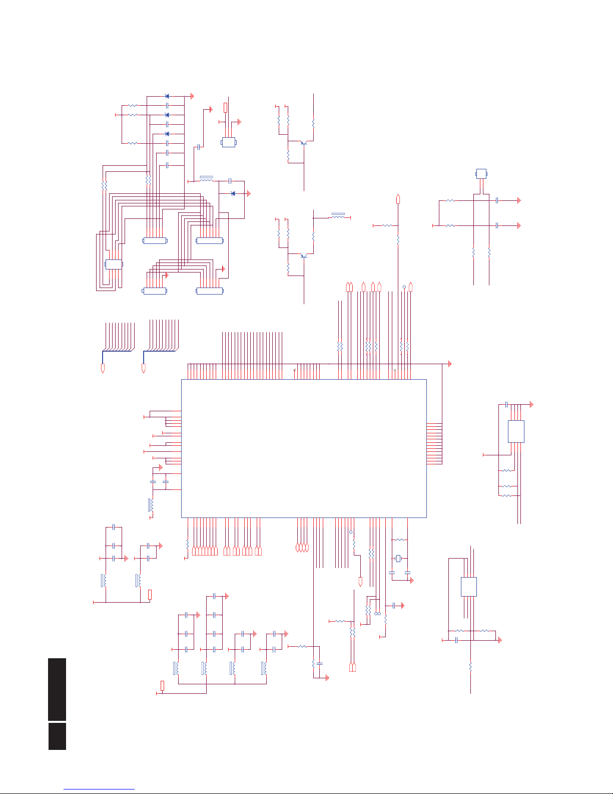
Meridian 3
Remark: Parts position can be searched by using FIND function in PDF.
C718
220N16V
TO-252
TO252
R716
NC/ 10K 1/ 16W 5%
R723
NC/4K7 1/16W 5%
Q707
NC/PMBS3904
DIM
ON/OFF
PS_EN 5
R717
NC
R720
NC
C717
NC/ 0. 1uF 25V
R725
NC
R724
NC
R799
10K 1/16W 5%
R798
NC
Q705
NC
C709
NC/ 0. 1uF 25V
R707
4.7 OHM +-5% 2WS
U702
NC/G1084-33T43Uf
VOUT
2
VIN
3
GND
1
C713
100NF 25V
C704
100NF 25V
R712 NC
R704
10K 1/16W 5%
CN701
CONN
123456789
R715
56KOHM 1/16W
R706
NC
R722
NC/ 10K 1/ 16W 5%
Audio_EN1
R711 NC
C701
100NF 25V
R713
NC
+
C702
100uF16V
Q704
AO4411
S
1
S
2
S
3
G
4
D
8
D
7
D
6
D
5
R703 1K 1/16W
C712
100NF 25V
C714
NC/0.1uF 25V
+
C705
100uF16V
R710
NC
R718
NC
+
C711
NC/100uF/16V
C708
NC
R714
10K 1/16W 5%
Q703
NC/PMBS3904
R709
NC
C703
100NF 25V
Q702
NC
C706
100NF 25V
R702
10K 1/16W 5%
+
C710
100uF16V
U703
AME8815BEGT180Z
GND
1
VOUT(heat sink )
2
VIN
3
4
4
C707
100NF 25V
R721
10K 1/16W 5%
R708
NC
U704
VIN
3
VOUT
2
GND
1
+
C716
10uF 50V
C715
220N16V
U701
VIN
3
VOUT
2
GND
1
on_BACKLIGHT 5
Adj_BACKLIGHT 5
VCC3.3 5
VLCD 6
VCC1.8 5
+5V3,4,5
Audio_EN 5
Panel_ON5
+5V 3,4,5
VLCD
VCC3.3
VCC3.3+5V
VCC3.3
+5V
VCC3.3
+5V
VCC3.3
+5V
VCC1.8
+5V
Q701
2N3904S-RTK/PS
Q706
2N3904S-RTK/PS
R719
22K 1/16W 5%
R701
22K 1/16W 5%
+5V
Audio_DET 5
FB701
300OHM
1 2
Audio_DET2Audio_DET1
POWER
Page 23

23
Meridian 3
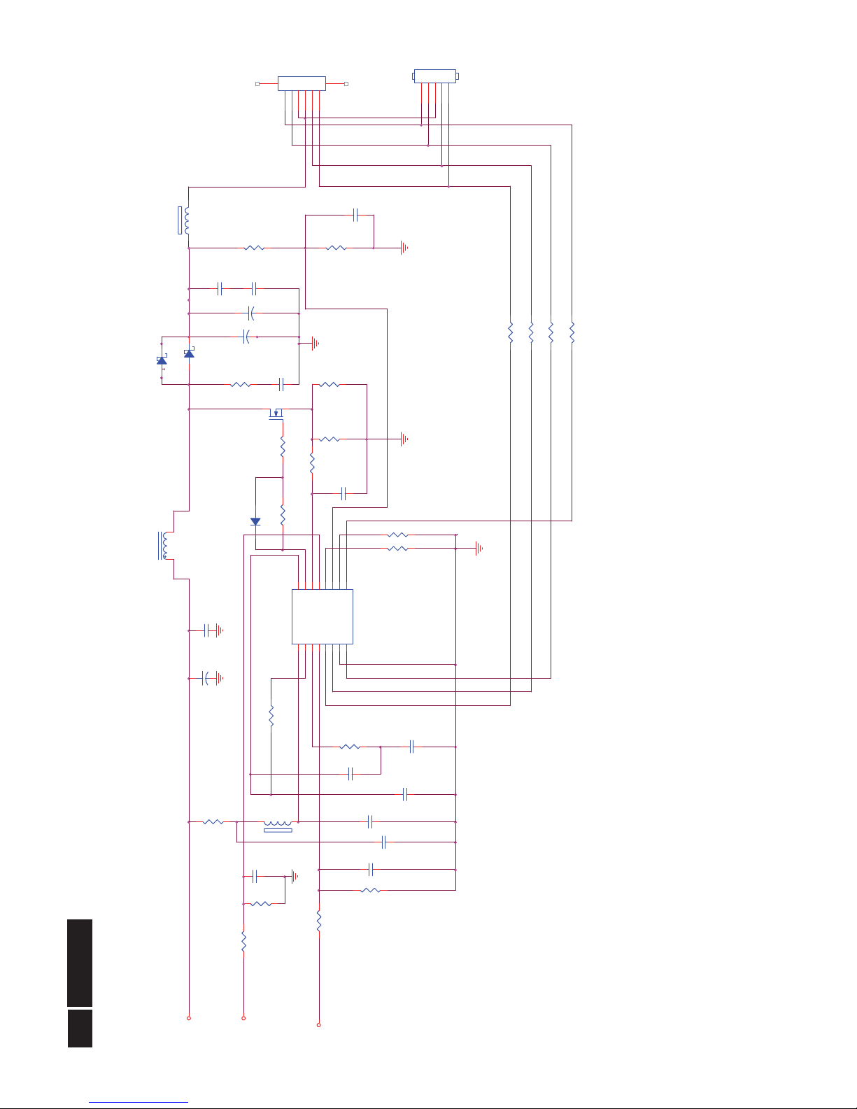
6.2 Power Board (715G3727P02006003S)
Remark: Parts position can be searched by using FIND function in PDF.
R911
10 OHM 1/4W
R907
100K OMH 2W +-5%
L904
3.5uH
C913
47N 50V
C911
NC/1500PF2KV
D910
NC/FME-220A
1
2
3
NC/ZD922
GDZJ5. 6B
1 2
R927
3.3K +-1% 1/10W
L905
NC/30MH
1
2
4
3
+16V
+5V
R908
1K 1/8W
C921
NC/1000PF/250VAC
Q903
KTD1028
+
C905A
150uF M 450V
3D_SW
R823
NC/0 OH M 1/ 8W
NC/D 904
BAV70
3
1
2
D903
1N4148
F904
T4AL 250V
-
+
BD902
NC/GBU408
2
1
3
4
+
C918
680UF25V
CN904
Wire Harnes s
123456789
101112
+
C939
680uF25V
-
+
BD901
GBL408
2
1
3
4
FB902
BEAD
1 2
R938
10K 1/8W 1%
C933
100N 50V
ON/OF F
+5V
DIM
C909
330P 50V
R910
10 OHM 1/4W
R939
1K 1/8W
IC901
LD7576AGR
CT1COMP2CS3GND
4
OUT
5
VCC
6
NC
7
HV
8
R905
5.1K 1/4W
FB903
BEAD
1 2
C942
2200pF 500V
R912
470 OHM
L903
3.5uH
!
C943
2200pF 500V
R909
1 OHM 1/4W
!
C903
0.47UF275V
NC/Q904
DTC144WKA
C907
0.1uF 50V
+
NC/C905
150uF 450V
+
C944
680uF25V
F901
T4AL 250V
3D_SW
NC/ZD921
TZX20B
1 2
CN901
SOCKET
12
3
R904
5.1K 1/4W
R943
470 OHM 1/8W
C932
1nF 50V
R925
1K 1/8W 1%
CN802
NC/CONN
1
2
DIM
R91947 OHM 1/4W
+16V
ON/OFF
CN801
NC/CONN
12345
!
!
!
R940
56K +-1% 1/10W
ZD902
TZX18B
1 2
C900
1000PF/250VAC
!
R92047 OHM 1/4W
!
HV
t
NR902
NTCR
12
R914
0.27OHM 5% 2W
T901
80GL32P 6 N
2
3
4
5
6
7
8
91011
12
F903
T5AL 250V
R903
680K 1/4W
C930
100N 50V
C904
NC/0. 22UF275V
R93547 OHM 1/4W
For INVERTER /
USB*4(option)
C901
680PF 250V
For MAIN/AUDIO
Circuit
LOAD=16V/3.0A
LOAD=5V/2.85A
C906
1500PF2KV
C937
NC/100pF/2KV
!
!
!
!
!
!
!
!!
!
+
C941
680uF25V
FB901
BEAD
12
L901
7mH
1
4
2
3
R96147 OHM 1/4W
RV903
NC
R902
680K 1/4W
L902
4mH
1
2
4
3
R946
820 OHM 2W
R906
5.1K 1/4W
R96247 OHM 1/4W
t
NR901
NC/NTCR
12
R947
820OHM
D909
FME-220A
1
2
3
R928
NC/0R05 7A 1/4W
090626
IC903
TLP78 1F
1
23
4
R924
200OHM +-5% 1/8W
+
C917
680UF25V
+
C908
47uF 50V
+
C916
680UF25V
C915
470uF 16V
IC904
AS431AZTR-E1
NC/R913
1K 1/8W 1%
R901
680K 1/4W
CN903
NC/33A3802-4
123
4
D901
PS102R
C928
1N 50V
C924
0.1uF 50V
+16V
Q901
STP10NK70ZFP
R926
2K1/10W
C902
680PF 250V
R930
2.4K 1/10W
GND1
GND
1
2
D900
BYV26EGP
1 2
R921NC
D907
FMX-12SL
1
2
3
R923NC
R922NC
C912
2200pF 500V
C929
2200pF 500V
D906
FMX-12SL
1
2
3
R91847 OHM 1/4W
POWER
Page 24
!
24
Meridian 3
Remark: Parts position can be searched by using FIND function in PDF.
R815
1M 1% 1/8W
R816
30K 1/8W 1%
C810
0.47UF 50V
+
C801
330UF 35V
C814
100N 50V
+16V
R802
300K 1/8W
R827
2R2 OHM 1/8W
R806
100 OHM 1% 1/10W
R801
10K 1/8W
D802
1N4148
D803 SK510B
1 2
Q801
AOD478
R809
330K +-1% 1/8W
C803
1N 50V
+
C817
4.7UF 100V
L801
33UH
2
4
U801
OZ9998BGN
ISEN113ISEN214GND15ISEN3
16
ISEN4
1
ISET
2
OVP
3
RT
4
ENA
5
ISW
6
LDR
7
VREF
8
VIN9STATUS10SSTCMP11PWM
12
R812
0.2oHM 1% 1/4W
R813
0.2oHM 1% 1/4W
C805
2.2U16V
C815
1N 50V
CN805
NC
12345
C804
0.47UF 50V
D801
NC/SK510B
1 2
CN804
CONN
12345
6
7 8
C811
0.47UF 50V
R804
10 OHM 1/8W
FB801
BEAD
1 2
FB802
BEAD
1 2
C812
100PF 50V
R819
1 OHM +-5% 1/8W
R822
1 OHM +-5% 1/8W
R821
1 OHM +-5% 1/8W
R820
1 OHM +-5% 1/8W
C808
100PF 500V
R805
100K 1/10W
C807
0.47UF 50V
R817
680 OHM 1/4W
R807
7.5 OHM 1/4W
ON/OFF
DIM
C802
10N 50V
R814
10 OHM 1%
+
C809
4.7uF100V
C806
220N 50V
R810
12K 1/8W 1%
R803
300K 1/8W
R818 10K 1/8W
C813
680nF 50V
CONVERTER
Page 25

25
Meridian 3
6.3 Key Board (715G4512K02000004S)
Remark: Parts position can be searched by using FIND function in PDF.
Button_3
Button_1
T01
T03
T02
T04
T05
C001
1000pF 50V
R007
680OHM +-5% 1/10W
ZD001
NC/UDZSNP5.6B
1 2
ZD002
NC/UDZSNP5.6B
1 2
Button_5
LED_Amber
LED_Blue
C003
0.1UF50V
R003 560OHM +-5% 1/10W
R002 560OHM +-5% 1/10W
R004 560OHM +-5% 1/10W
R005 560OHM +-5% 1/10W
Button_1
Button_2
Button_3
Button_5
Button_4
ZD003
NC/UDZSNP5.6B
1 2
LED_Vcc
Button_4
I2C_SDA
White
Yellow
LED001
LED
1
2 3
4
I2C_SCL
C002
10uF 6. 3V
Button_2
CN001CN401
4
3
2
1
7
6
5
POWER KEY#
KEY1
R006
NC
LED G
KEY2
LED R
GND
I2C SCL
I2C SDANCLED VCC
NC
GND
VCC
R001 560OHM +-5% 1/10W
RIGHT INPUT
POWER
LEFTMENU
Buttons
U001
CG7246AM
GP0[0]1GP0[1]2I2C SCL3I2C SDA
4
GP1[0]
5
GP1[1]
6
VSS
7
GP1[2]
8
GP1[3]9GP1[4]
10
XRES
11
GP0[2]
12
VDD
13
GP0[3]
14
CSInt
15
GP0[4]
16
VCC
LED_Blue
ZD004
NC/UDZSNP5.6B
1 2
LED_Amber
CN001
CONN
12345
6
78
VCC
I2C_SCL
I2C_SDA
RIGHT
MENU
LEFT
Power
INPUT
Key-pad-switch
Page 26

!
26
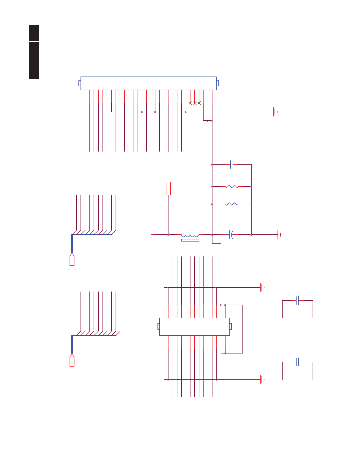
Meridian 3
7. PCB Layout
7.1 Scaler Board (715G3737M02000004K)
Remark: Parts position can be searched by using FIND function in PDF.
VIA6
SEN2
SEN3
SEN1
HOLE1
SEN4
VIA20
VIA21
VIA22
VIA25VIA30
VIA31
VIA37 VIA39VIA40
VIA43VIA44
VIA45VIA46
VIA47
VIA48
VIA51VIA52VIA55VIA58
VIA63
VIA64
VIA79VIA80VIA81VIA82VIA83VIA84 VIA92VIA93VIA94
VIA95VIA96VIA97
VIA98VIA99VIA100
VIA73VIA74VIA87
VIA1
VIA2
R2 R3
D101
FB404
FB401
FB402
FB403
FB407
U101
U402
U403
U701
R421
R105
R106
R107
R101
R111
R112
R113
R114
R115
R116
R123 R124
R125
R119
R120
R121
R126
R127
R128R129
R130
R131
R136
R132
R137
R138
R134
R133
R135
R139
R423
R406
R407
R401
R409
R411
R412
R413
R415
R416
R419
R420
R422
R424
R426
R429
R430
R441
R442
R438
R439
R702
R703
R704
R706
C102
C103 C104
C105
C106 C107
C108
C109
C110
C111
C113
C112
C114
C116
C115
C117
C417
C403
C430
C405
C703
C407
C408
C704
C409
C410
C411
C412
C706
C707
C714
C401
C418
C420
C422
C717
C431
C432
C427
C709
C701
C708
D404
R404
R108
CN408
C101
R710
X401
R434
Q401
Q701
C434
C435
R402
R432
R431
R428
R427
SCREW1
R140
R709
C118
C119
C402
C436
R448
C419
C712
C433
CN403
CN701
U103
U104
U102
U107
U106
Q702
R721
R722
R449
Q703
C429
CN405
CN404
CN406
R414
R425
R433
U702
C713
U704
CN101
CN102
C705
C710
C711
U401
D401
D402
D403
ZD101
ZD102
CN407
CN402
CN401
C425
C426
C428
C715
C718
C404
C413
C416
C421
C423
C702
C716
R102
R141
R403
R405
R435
R436
R437
R443
R444
R701
R708
R711
R712
R713
R714
R715
R716
R717
R718
R719
R720
R723
R122
R417
FB405
FB406
FB408
FB409
Q704
U105
U703
D102Q101
Q402
Q706
Q707
C120R142
R451
R452
R724
R725
CN409
C414
R408
C406
C415
C424
R418
R103 R104
R109
R110
R117
R118
R410
R440
R446
C181
C182
R798
R799
TP1
TP3 TP4
TP5
Q705
C437
FB701
FB410
R707
Remark: Parts position can be searched by using FIND function in PDF.
Page 27

27
Meridian 3
7.2 Power Board (715G3727P02006003S)
Remark: Parts position can be searched by using FIND function in PDF.
PIN35
PIN34
PIN7
PIN26
PIN1
PIN2
R2
R6R9
R1
R4
R5
PIN3
PIN6
PIN14
PIN19
PIN20
C903
H3
F901
F903
CN903
L904
L903
FB1
BD901
D909
D906
R914
L901
L902
Q901
NR901
RV903
C905
T901
CN802
HS1
NR902
C905A
D907
C904
CN804
L905
D910
D903
ZD902
ZD921
ZD922
L801
IC904
IC903
C912
C929
C943
C942
C906
C911
C937
S1
S3
S4
J805
J816
J901
J902
J903
J804
J905
J927
J908
J928
J913
J815
FB901
FB902
FB903
CN901
FB801
J808
J814
GND1
L802
L803
D802
FB802
J810
J926
J918
J817
J802
J930
J929
J809
J910
J803
HS3
HS2
CN904
J801
J807
J811
J806
J812
Q903
D901
D900
R907
R946
R947
HS4
C901
C902
C900
C915
C916
C917
C918
C939
C941
C944
C945
C946
C921
C908
C809 C817
C801
CN805
CN801
CN806
D803
F904
J909
C818
C819
R915
Remark: Parts position can be searched by using FIND function in PDF.
R7R10
PIN4
PIN5
PIN8 PIN9
PIN10PIN11
PIN12
PIN13
PIN15
PIN16
PIN17
PIN18
SG9
SG4
R926
R927
R930
R940
C932
C909
C924
C928
C913
C930
SEN3
SEN5
SEN8
SEN1
IC901
C802
C803
C804
C805
C806
C807
C810
C811
C812
C813
C814
C815
C933
C808
D904
Q803
Q801
RJ806
RJ803
RJ802
R805
R806
C816
U801
R921
R901
R902
R904 R905
R909
R910
R912
R918
R919
R920
R935
R961
R962
R903
R911
R906
R922
R923
R812
R813
R817
R928
R807
D801
R814
R820
R924
R925
R938
R939
R943
R913
R801
R802
R803
R804
R809
R810
R815
R816
R818
R822
R821
R819
R823
R908
R824
R826
R825
R827
Q904
JR901
C907
R829
R830
R828
Page 28

!
28
Meridian 3
7.3 Key Board(715G4512K02000004S)
Remark: Parts position can be searched by using FIND function in PDF.
C001
C002
C003
CN001
R001
R002
R003
R004
R005
R007
T01
T02
T03
T04
T05
U001
LED001
U1
T1
T6
Page 29

29
Meridian 3
8. Wring Diagram
Panel
1
Power Board
CN904
CN804
Key Board
CN001
6
1
1
6
CN901
Scaler Board
CN409
CN701
CN404
1
5
1
12
CN101
CN102
Page 30

!
30
Meridian 3
9. Scaler Board Overview
FFC Cable
D-SUB EEPROM
DVI EEPROM
DC-DC
ScalerIC
Page 31

31
Meridian 3
10. Mechanical Instructions
Step 1: Remove the stand-base ASSY
1. Remove the two screws to remove the stand-base
ASSY.
Step 2: Remove the rear cover
1. Use disassembly tool to open all the latches along
the edge of the Rear Cover
Step 3: Remove the mainframe and the boards
1. Disconnect all the connectors and remove the four
screws to remove the mainframe.
2. Remove the eight screws to remove the scaler board
and the power board.
Page 32

!
32
Meridian 3
3. Kick off the shield to remove the power board.
4. Disconnect the cables to remove the scaler board
and the power board.
The scaler board
The power board
Step 4: The panel
Step 5: The bezel
Page 33

33
Meridian 3
11. Repair Flow Chart
1. No Power
OK
NG
No power
Check power cable is
tightened?
Check Power “On/Off”
is “On”?
Re-plug the power cable
Replace main board and check connections
Check the LED
indicator is OK?
Check the AC power
Replace the power board and check connections
OK
NG
OK
NG
NG
Turn on the Power “On/Off” switch
Replace key board and check connections
NG
Page 34

!
34
Meridian 3
2. Video (Power LED White)
No Video (Power LED White)
Press the power
button is OK?
Check the FFC cable
or panel
The end
NG
OK
OK
NG
Replace the main board
Replace the power
board and connection
Replace the FFC cable
or panel
NG
The end
Replace the key board
NG
OK
Replace the main
board and connection
OK
Page 35

35
Meridian 3
3. DIM
OK
The end
OK
The end
OK
The end
DIM (image overlap, focus or flicker)
Reset in factory mode
Set to the optimal
frequency, select the
recommended fre
q
uenc
y
Pull out signal cable and
check “Self Test Feature
Check” is ok?
Check the signal cable
and the PC
Readjust the phase and pixel
clock in the user mode
Replace the main board
Replace the panel
NG
NG
NG
OK
NG
NG
OK
The end
OK
NG
Page 36

!
36
Meridian 3
4. Color is not optimal
NG
Color is not optimal
Miss color
Color shift
Replace the signal cable
Pull out the signal cable
and check the screen
color display is normal?
The end
Replace the signal cable or PC
Reset the factory mode
In the user mode, set the “color
settings” until customer satisfy
Replace the main board
NG
OK
NG
OK
NG
Page 37

37
Meridian 3
12. ISP Instruction
When do the parts, need the tools as follow:
1. An i486 (or above) personal computer or compatible.
2. Microsoft operation system Windows 95/98/2000/XP.
3. ISP tool “ISP_Tool.exe”
4. USB port driver and Installation patch
5. ISP Board (715GT089-B/C) x1
6. USB cablex1, VGA cable x1
7. software
12.1. Connect the ISP board, PC and monitor as follow:
12.2 Install USB driver.
1. When insert the USB cable to PC USB port, will pop up a Hardware Wizard to help you install the USB driver if you
use this ISP board first time. You can install it successfully as the below instruction step by step.
Remark: The USB driver files path: D:\FTC100103(Mstar)\FTCUSB.INF
Page 38

!
38
Meridian 3
Click “Finish” to
complete the
USB serial port
driver
installation.
Page 39

39
Meridian 3
12.3. Install the ISP tool.
1. Double-click to install ISP program.
2. Double-click
to run the ISP tool.
3. Set the parameters to restore the HDCP key if the monitor has DVI or HDMI port.
(1) Click the “Option” item.
(2) Tick “FE2P Mode Enable”.
Page 40

!
40
Meridian 3
(3) Tick “Enable Auto FE2P Detect”.
4. Setup ISP tool. Click “Setup ISP tool” to open the configuration window.
5. Configuration for ISP tool. Tick “FTDI”.
6. Load the F/W you want to upgrade.
Page 41

41
Meridian 3
7. Start to program. Click “Auto” to start programming.
Page 42

!
42
Meridian 3
4.8. Programing success. There will be the message in the red frame after successful programming.
12.4. Check the FW version after upgrade.
1. The way to open factory menu.
(1)Connect video source to monitor and AC on.
(2)The way to factory menu: Press “MENU” and “+” keys synchronously (The rightmost and left most keys in the
touch keyboard), and DC on. When the screen lights, release the two keys and press “MENU” again to ope n
factory menu.
“+” key DC key “menu” key
(3)Select “factory” and press menu key to open factory menu as below.
Page 43

43
Meridian 3
(4)Please do “Auto Color” in factory menu after change main board and upgrade F/W.
2. Do factory reset in user menu. User menu – Setup – Reset - Yes.
(1) Restart the monitor after open factory menu. And then open the user menu.
(2) Factory reset will turn off “Burn in” mode which screen color switches among red, green, blue and black.
12.5. Troubleshooting.
1. “CheckSum Comparing Fail!” error.
Method: Tick the “Send MX2060 CMD” at Option item.
Check this F/W
version.
Page 44

!
44
Meridian 3
2.When can’t upgrade, please retry below several ways to upgrade.
(1) When the tool appears erase error, you can change another version tool to try.
(2) The program must be in the monitor standby state, while the fail communication with monitor might result the
monitor power off. In this situation, you may AC off the monitor for a while and then AC on to retry. Maybe the
defect will be cured.
(3) Change ISP JIG or cable.
(4) Change PC
Page 45

45
Meridian 3
13. DDC Instruction
1. An i486 (or above) personal computer or compatible.
2. Microsoft operation system Windows 95/98/2000/XP.
3. LPT port driver “PORT95NT.exe” and EDID tool “VgaSinglePort.exe”
4. EDID Board (715GT034-B) x1,
5. LPT cable (male to male) x1, VGA cable x 1
6. 12V DC adapter
7. EDID data
13.1 Connect the ISP board, PC and monitor as follow:
13.2 Install LPT drive
1. Double click the icon to install the driver.
2. Restart PC after installation.
13.3 Prepare the EDID written
1. Change the EDID files name as below rule.
Anolog EDID WA.dat Digital EDID WD.dat
2. Copy these three files to one folder named as Philips 273E3L which must contains “config.ini” file.
Page 46

!
46
Meridian 3
3. Copy Philips 273E3L to DDC folder and put DDC and ISP tool together.
13.4 Run the ISP tool
1. Double-click the icon to open the tool.
2. Tick the “Analog+DVI” a nd click “Loadfile” to set the parameters.
(1).Tick “Analog”, and “Digital” .
(2).Manufacturer: PHL Product Code: C077 Model Name: Philips 273E3
Page 47

47
Meridian 3
3. Select the EDID folder. Select correct folder.
Page 48

!
48
Meridian 3
4. Load EDID successful. In the EDID tool, you can know the EDID information.
5. Tick the “Only connect VGA” and “Write SN”, and type in the 14 digit S/N and date.
Page 49

49
Meridian 3
6. Start writing. Click “Program” to start writing. When the green “PASS” appear, the process is finished.
7. Check the S/N in monitor user menu.
Press “MENU” and select “Input” you can check the SN in the botton of menu interface.
Page 50

!
50
Meridian 3
13.5. Troubleshooting.
1. Can’t write error.
2. Try below few ways to cure can’t write errors!
(1) AC on the monitor and turn on it.(Restart the monitor)
(2)Take apart the monitor and connect the 7pin of EEPROM to GND to diable write protection then write EDID one
by one.
(3)Set the Burn in on last to try again.
Page 51

51
Meridian 3
273E3LSW/93 EDID
Analog
00 01 02 03 04 05 06 07 08 09 0A 0B 0C 0D 0E 0F
-----------------------------------------------
00| 00 FF FF FF FF FF FF 00 41 0C 77 C0 01 01 01 01
10| 00 13 01 03 6E 3C 22 78 2E CA 45 A4 56 4B 9C 25
20| 12 50 54 BD 4B 00 D1 C0 B3 00 95 00 81 80 95 0F
30| 01 01 01 01 01 01 02 3A 80 18 71 38 2D 40 58 2C
40| 45 00 56 50 21 00 00 1E 00 00 00 FF 00 0A 20 20
50| 20 20 20 20 20 20 20 20 20 20 00 00 00 FC 00 50
60| 68 69 6C 69 70 73 20 32 37 33 45 33 00 00 00 FD
70| 00 38 4C 1E 53 11 00 0A 20 20 20 20 20 20 00 A7
EDID Structure Version/Revision: 01 03
<-Vendor/Product Identification:->
ID Manufacturer Name: PHL
ID Product Code: C077
ID Serial Number: No Use
Week of Manufacture: 0
Year of Manufacture: 2009
<-Basic Display Parameters/Features:->
Video i/p definition: Analog
Max. H. Image Size : 60cm
Max. V. Image Size : 34cm
Display Gamma : 2.2
<-Color Characteristics:->
Rx: 0.644 Gx: 0.295 Bx: 0.146 Wx: 0.313
Ry: 0.336 Gy: 0.611 By: 0.070 Wy: 0.329
<-Established Timings:->
Established Timings 1:BD
720 x 400 @ 70Hz VGA,IBM
640 x 480 @ 60Hz VGA,IBM
640 x 480 @ 67Hz Apple,Mac II
640 x 480 @ 72Hz VESA
Page 52

!
52
Meridian 3
640 x 480 @ 75Hz VESA
800 x 600 @ 60Hz VESA
Established Timings 2:4B
800 x 600 @ 75Hz VESA
1024 x 768 @ 60Hz VESA
1024 x 768 @ 75Hz VESA
1280 x1024 @ 75Hz VESA
Established Timings 3:00
<-Standard Timing Identification:->
1920 x 1080 @ 60Hz
1680 x 1050 @ 60Hz
1440 x 900 @ 60Hz
1280 x 1024 @ 60Hz
1440 x 900 @ 75Hz
<-Detailed Timing Descriptions:->
FC (Monitor Name) : Philips 273E3
FD (Monitor Limits):
Min. V. rate: 56 Hz
Max. V. rate: 76 Hz
Min. H. rate: 30 KHz
Max. H. rate: 83 KHz
Max. P Clock: 170 MHz
FF (Monitor SN) :
Detailed Timing : 1920x1080 @ 60Hz
Extension Flag : 00
Block0 Checksum : A7
Dightal
00 01 02 03 04 05 06 07 08 09 0A 0B 0C 0D 0E 0F
-----------------------------------------------
00| 00 FF FF FF FF FF FF 00 41 0C 77 C0 01 01 01 01
10| 00 13 01 03 80 3C 22 78 2E CA 45 A4 56 4B 9C 25
20| 12 50 54 BD 4B 00 D1 C0 B3 00 95 00 81 80 95 0F
Page 53

53
Meridian 3
30| 01 01 01 01 01 01 02 3A 80 18 71 38 2D 40 58 2C
40| 45 00 56 50 21 00 00 1E 00 00 00 FF 00 0A 20 20
50| 20 20 20 20 20 20 20 20 20 20 00 00 00 FC 00 50
60| 68 69 6C 69 70 73 20 32 37 33 45 33 00 00 00 FD
70| 00 38 4C 1E 53 11 00 0A 20 20 20 20 20 20 00 95
EDID Structure Version/Revision: 01 03
<-Vendor/Product Identification:->
ID Manufacturer Name: PHL
ID Product Code: C077
ID Serial Number: No Use
Week of Manufacture: 0
Year of Manufacture: 2009
<-Basic Display Parameters/Features:->
Video i/p definition: Digital
Max. H. Image Size : 60cm
Max. V. Image Size : 34cm
Display Gamma : 2.2
<-Color Characteristics:->
Rx: 0.644 Gx: 0.295 Bx: 0.146 Wx: 0.313
Ry: 0.336 Gy: 0.611 By: 0.070 Wy: 0.329
<-Established Timings:->
Established Timings 1:BD
720 x 400 @ 70Hz VGA,IBM
640 x 480 @ 60Hz VGA,IBM
640 x 480 @ 67Hz Apple,Mac II
640 x 480 @ 72Hz VESA
640 x 480 @ 75Hz VESA
800 x 600 @ 60Hz VESA
Established Timings 2:4B
800 x 600 @ 75Hz VESA
1024 x 768 @ 60Hz VESA
1024 x 768 @ 75Hz VESA
1280 x1024 @ 75Hz VESA
Page 54

!
54
Meridian 3
Established Timings 3:00
<-Standard Timing Identification:->
1920 x 1080 @ 60Hz
1680 x 1050 @ 60Hz
1440 x 900 @ 60Hz
1280 x 1024 @ 60Hz
1440 x 900 @ 75Hz
<-Detailed Timing Descriptions:->
FC (Monitor Name) : Philips 273E3
FD (Monitor Limits):
Min. V. rate: 56 Hz
Max. V. rate: 76 Hz
Min. H. rate: 30 KHz
Max. H. rate: 83 KHz
Max. P Clock: 170 MHz
FF (Monitor SN) :
Detailed Timing : 1920x1080 @ 60Hz
Extension Flag : 00
Block0 Checksum : 95
Page 55

55
Meridian 3
14. White Balance, Luminance Adjustment
1. Apparatuses and program: analyzer CA-210, PC, tool, FGA adjustment program (Philips LEDFGA.DDCI),
Pattern generator.
2. Equipment installation:
a. Connect analyzer CA-210 to PC by USB connector, install drive program CA-SDK Ver4.00 for CA-210 and restart
PC after finish installing
b. Install Port95NT drive program, set PC printer connector mode as ECP mode and reset PC after finish installing.
c. Connect tool as follow:
Note: It’s not necessary to connect Port2.
3. Adjustment
Preparation before adjustment:
a. Monitor should be warmed up for more than half an hour .
b. Make sure that the tools are connected right and drive programs have been installed OK.
4. Adjustment process:
a. Press the power of CA-210, shut off the lens, press 0-Cal and open the lens after analyzer reset.
b. Open white balance adjustment program, select the right parameter according with the program and click OK.
c. Make sure that the lens of CA-210 aims at the center of the screen, then click START to adjust.
d. After finish adjusting, the adjustment program displays pass, and the START button changes for NEXT, which
means that you can adjust another monitor.
To PC LPT
To BSG-265A or
e
q
uivalent instrument
To PC Port 2
Philips model
Page 56

!
56
Meridian 3
5. Color Temp confirmation
Connect the signal to the monitor, the monitor displ ays white-picture, use CA-210 to measure the Color Temp of the
screen center and select the OSD to make sure whether the Color Temps accord with the SPEC.
CIE
coordinates
9300K 6500K/sRGB sRGB
x 0.283±0.02 0.313±0.02 0.313±0.02
y 0.297±0.02 0.329±0.02 0.329±0.02
6. How to enter into the factory mode:
1. Connect the video source and power off the monitor.
2. Press and buttons at the same time, power on the monitor, and then press the menu again; the
picture will appear on the top left corner.
3. Select the “Factory” and press the “MENU” button to enter the factory mode.
Page 57

57
Meridian 2
15. Monitor Exploded View
Item Description
1 DECO_BEZEL_R
2 DECO_BEZEL_L
3 BEZEL
4LENS
5 KEY BOARD ASSY
6 PANEL
7 POWER BOARD ASSY
8 SCALER B O A RD AS SY
9 MAINFRAME
10 REAR_COVER
11 HINGE 27
12 STAND
13 BASE L27W-TS30-tss10
Page 58

!
58
Meridian 3
16. Recommended & Spare Parts List
Note: Take the 273E3LSW/93 BOM for example, the parts information listed below are for reference only, and are
subject to change without notice. Please go to http://cs.tpv.com.cn/hello1.asp
for the latest information
Item Location PCM Codes Description Remark
1 FQ141 A33G1192BPQ 3L0200 DECO_BEZEL_R
2 FQ142 A33G1193BPQ 3L0200 DECO_BEZEL_L
3 FQ106 A34G2413BPJB2B0230 BEZEL
4 FQ411 A33G1137 3 1C0100 LENS
5 FQ004 KEPCAQP6 KEY BOARD ASSY
6 E750 750GBU270H1213N000 PANEL
7 FQ003 PLPCB1606QFC POWER BOARD ASSY
8 FQ002 CBPCANRPHQL SCALER BOARD ASSY
9 FQ124 A15G0887401201 MAINFRAME
10 FQ105 Q34G7434ADSBBB0100 REAR_COVER
11 M037 A37G0135 1 HINGE 27
12 FQ125 A34G1481BPJ 1B0100 STAND
13 FQ109 A34G2414BPJ 1B0133 BASE L27W-TS30-TSS10
E08903 089G1745CAB AC DVI CABLE 1500MM
E08903 089G1745HAB AC DVI CABLE
E08901 089G414C15N IS POWER CORD I-SHENG
ECN804 095G8014 6D 69 HARNESS 6P-6P(CI1406S) 250MM
ECN804 095G8014 6X 69 HARNESS 6P-6P(CI1406S) 250MM
E09502 095G8014 7W614 HARNESS 7P(PLUG)-6P(A1253HA HR) 180MM
E09502 095G8014 7X614 HARNESS 7P(PLUG)-6P(A1253HA HR) 180MM
ECN408 395G179X30NH76 FFC CABLE 30PIN 259 1.0MM
E750 750GBU270H1223N000 LCD M270HW01 V20A XM AUO
FQ201 Q40G 27N813 5A RATING LABEL
FQ208 Q41G780081378G WARRANTY CARD WARRANTY CARD FOR CHINA
FQ206 Q41G78S181339A 273E3L/273E3LH QSG (M3273ELQ1T)
FQ205 705GQCCS044141 EPS ASSY
Q44GF015103 CUSHION-T EPS
Q44GF015203 CUSHION-B EPS
FQ202 Q44GF01581310A ARTWORK CARTON 273E3LSW
FQ212 Q45G 88609196 EPE BAG
FQ215 Q45G9901609231 P.E. BAGX430X300X0.5
FQ204 Q70G27C181303E CD MANUAL 273E3L
ECN408 S95G179T30NH76 FFC CABLE 30PIN 1.0MM 260MM
FQ220 Q40G000181313A CARTON LABEL
M037 SA37G01351 HINGE ASS'Y
FQ002 756GQCCB0PH0560000 SCALER BOARD ASSY(CBPC*)
U402 100GPNAG004N11 MCU ASSY(056G2233 11)
Page 59

59
Meridian 3
CN404 033G3802 7B Y WAFER
CN701 033G3802 9B Y CONNECTOR 9P 2.0
CN701 033G3802 9B Y W WAFER
CN408 033G801930F CH L FFC CONN 1.0MM 30P R/A 34MM 6MM
CN408 033G801930F CH JS FFC CONN 1.0MM 30P R/A 34MM 6.3MM
R707 061G152M479 64 SH RST MOFR 4.7 OHM +-5% 2WS SANHUAN
R707 061G152M479 64 SY RST MOFR 4.7 OHM +-5% 2WS FUTABA
CN101 088G 35315F HD HF D-SUB CONN WITH SCREW 15P BLUE
CN101 088G 35315F XH HF D-SUB 15PIN VERTICAL CONN WITH SCREW
CN102 088G 35424FXNH HF DVI CONN WITH SCREW 24P WHITE - R/A 37.7
X401 093G 2251B J CRYSTAL 12MHZ NXS12.000AC30F-KAB10
C716 067G 3051007PB EC 10UF 20% 50V 5*11 CD263
C702 067G 3051013PB EC 105C 100UF M 16V 5*11MM JH CD263
C433 067G 3051013XB EC 100UF 20% 16V 5*11
U401 056G 562328 IC SCALER NT68668AUFG QFP-128
U701 056G 563149 IC G903T63UF 0.6A/3.3V SOT-223
U703 056G 563161 IC AME8815BEGT180Z 1.5A/1.8V SOT-223
U104 056G 662 52 ESD PROTECT AZC398-04S.R7G SOT23-6
U105 056G1133158 EEPROM CAT24C02WI-GT3A 2KB SOIC-8
U101 056G1133956 IC CAT24C02WI-GT3 SO-8
Q701 057G 417 12 T KEC 2N3904S-RTK/PS
Q401 057G 417 13 T SMALLTRAN 2N3906S-RTK/PS 0.2A 40V SOT-23
Q401 057G 417517 TRA LMBT3906LT1G -200MA/-40V SOT-23 LRC
Q701 057G 417518 TRA LMBT3904LT1G 200MA/40V SOT-23 LRC
Q704 057G 763 3 AO4411 SO-8 BY AOS
R409 061G0402000 JF RST CHIPR MAX0R05 1/16W FENGHUA
R103 061G0402000 JI RST 0402 0.05R MAX 1/16W
R409 061G0402000 JT RST CHIPR MAX0R05 1/16W TZAI YUAN
R141 061G0402100 JI TEST ONLY RST 0402 10R 5% 1/16W TA-I
R141 061G0402100 JT RST CHIP 10R 1/16W 5% TZAI YUAN
R101 061G0402101 JI BEST ONLY RST 0402 100R 5% 1/16W TA-I
R101 061G0402101 JT RST CHIP 100R 1/16W 5% TZAI YUAN
R703 061G0402102 JF RST CHIPR 1KOHM +-5% 1/16W FENGHUA
R703 061G0402102 JI RST 0402 1K 5% 1/16W TA-I
R419 061G0402103 JF RST CHIPR 10KOHM +-5% 1/16W FENGHUA
R799 061G0402103 JI TEST ONLY RST 0402 10K 5% 1/16W TA-I
R714 061G0402103 JT RST CHIP 10K 1/16W 5% TZAI YUAN
R415 061G0402104 JI TEST ONLY RST 0402 100K 5% 1/16W TA-I
R415 061G0402104 JT RST CHIP 100K 1/16W 5% TZAI YUAN
R432 061G0402105 JF RST CHIPR 1MOHM 5% 1/16W FENGHUA
Page 60

!
60
Meridian 3
R432 061G0402105 JI EST ONLY RST 0402 1M 5% 1/16W TA-I
R420 061G04021200FF RST CHIPR 120 OHM +-1% 1/16W FENGHUA
R420 061G04021200FT RST CHIP 120R 1/16W 1% TZAI YUAN
R411 061G0402222 JF RST CHIPR 2.2KOHM +-5% 1/16W FENGHUA
R125 061G0402222 JI TEST ONLY RST 0402 2.2K 5% 1/16W TA-I
R125 061G0402222 JT RST CHIP 2K2 1/16W 5% TZAI YUAN
R116 061G0402223 JI TEST ONLY RST 0402 22K 5% 1/16W TA-I
R116 061G0402223 JT RST CHIP 22K 1/16W 5% TZAI YUAN
R416 061G0402224 JF RST CHIPR 220KOHM +-5% 1/16W FENGHUA
R416 061G0402224 JT RST CHIP 220K 1/16W 5% TZAI YUAN
R408 061G04024700FF RST CHIP 470R 1/16W 1% FENGHUA
R408 061G04024700FT RST CHIP 470R 1/16W 1%
R142 061G0402471 JI TEST ONLY RST 0402 470R 5% 1/16W TA-I
R142 061G0402471 JT RST CHIP 470R 1/16W 5% TZAI YUAN
R114 061G0402472 JI TEST ONLY RST CHIP 4.7K 5% 1/16W TA-I
R114 061G0402472 JT RST CHIP 4K7 1/16W 5% TZAI YUAN
R715 061G0402563 JF RST CHIPR 56KOHM 1/16W FENGHUA
R715 061G0402563 JT RST CHIPR 56KOHM 1/16W TZAI YUAN
R120 061G04027509FF RST CHIPR 75 OHM +-1% 1/16W FENGHUA
R120 061G04027509FT RST CHIP 75R 1/16W 1%
R423 061G0402752 JI RST 0402 7.5K 5% 1/16W
R423 061G0402752 JT RST CHIP 7K5 1/16W 5% TZAI YUAN
R418 061G0603000 JF RST CHIPR MAX 0R05 1/10W FENGHUA
R122 061G0603000 JI RST 0603 0.05R MAX 1/10W TA-I
R122 061G0603000 JT RST CHIP MAX 0R05 1/10W TZAI YUAN
R448 061G1206221 JI RST 1206 220R 5% 1/4W
R448 061G1206221 JT RST CHIPR 220 OHM +-5% 1/4W TZAI YUAN
C120 065G040210232K 3 CAP CHIP 0402 1N 50V X7R +/-10%
C120 065G040210232K T CAP CHIP 0402 1000PF 50V X7R
C115 065G040210425K T CAP 0402 100NF 10% 25V X5R
C420 065G0402105A5K M CAP 0402 1UF 10% 10V X5R
C414 065G0402105A5K T CAP 0402 1UF 10% 10V X5R
C182 065G040222031J 3 CAP CHIP 0402 22P 50V NPO +/-5%
C426 065G040222031J A CAP 0402 22PF J 50V NPO
C426 065G040222031J T CAP CHIP 0402 22PF J 50V NPO
C429 065G040222415K 3 NDS-ASSIGN CAP CHIP 220NF 16V X5R
C718 065G040222415K T CAP CHIP 0402 220NF K 16V X5R
C428 065G040227031J A CAP 0402 27PF 5% 50V NP0
C428 065G040227031J T CAP CHIP 0402 27PF 50V NPO
C102 065G040247312K 3 CHIP CAP 47NF16V X7R 10%
Page 61

61
Meridian 3
C110 065G040247312K T CAP 0402 47NF 10% 16V X7R
C103 065G040250931C A CAP 0402 5PF 0.25PF 50V NP0
C103 065G040250931C Y CAP 0402 5PF 0.25PF 50V NP0
C404 065G0805475A2K T CAP CHIP 0805 4.7UF K 10V X7R
C404 065G0805475A2K Y NO-SUGGEST CAP 0805 4.7UF 10% 10V X7R
FB409 071G 56K121 M CHIP BEAD 120OHM 6A MGLB2012-120T-LF
FB701 071G 56V301 M CHIP BEAD 0805 300R 25% 700MA
FB701 071G 56V301 TA CHIP BD 0805 300R/700MA FCM2012VF-301T07
D101 093G 64 42 L DIODE LBAV70LT1G SOT-23 LRC
D102 093G 64 42 P BAV70 SOT23 BY PAN JIT
D402 093G 39GA01 T RLZ5.6B
D403 093G 39S 24 T RLZ 5.6B LLDS
CN001 033G8032 6F S HR CONNECTOR
U001 056G 669 10 TOUCH KEY CG7246AMT QFN-16(COL)
R005 061G0603561 JI RST 0603 560R 5% 1/10W
R001 061G0603561 JT RST CHIPR 560OHM +-5% 1/10W TZAI YUAN
R007 061G0603681 JI RST 0603 680R 5% 1/10W
R007 061G0603681 JT RST CHIPR 680OHM +-5% 1/10W TZAI YUAN
C001 065G060310231J 3 CAP 0603 1N 50V NPO +/-5%
C001 065G060310231J Y CHIP 0603 1000PF 50V NPO
C003 065G060310432K 3 CAP CHIP 0603 0.1UF K 50V X7R
C003 065G060310432K F CAP CHIP 0603 0.1UF K 50V X7R
C002 065G060310605M T CAP 0603 10UF 20% 6.3V X5R
C002 065G060310605M Y NO-SUGGEST CAP 0603 10UF 20% 6.3V X5R
LED001 081G 14 30 EL CHIP LED YELLOW / WHITE
LED001 081G 14 30 GP CHIP LED YELLOW/WHITE GPTD1205YW1-F
IC903 056G 139 10 IC TLP781F PHOTOCOUPLER DIP-4
IC903 056G 139 3A PC123Y22FZOF SHARP
NR902 061G 58809MEN RST NTCR 8OHM +/20%/NMM01 4A XIANZHENG
R914 061G 20J278GB1 SY RST CEM 0.27OHM 5% 2W
C903 063G107K474 6S 0.47UF +-10%
C903 063G107K474 UM CAP X2 470NF 10% 275V
C905A 067G 41Z15115L EC 150UF 450V 20% 20*45
L901 073G 174 65 H LINE FILTER 7MH MIN GBQM4.778.406
L901 073G 174 65 X LINE FILTER 7MH MIN 3TRET20-702M
L902 073G 174 76 H LINE FILTER DADON
L902 073G 174 76 LP LINE FILTER 4MH MIN VOC
L801 073G 174266 CP BOOST CHOKE 25UH 10% 3.8A L020477-6
L904 073G 253 91 H IND CHOKE 3.5UH+-10% DADONG
L903 073G 253 91 V CHOKE COIL 3.5UH+-10%
Page 62

!
62
Meridian 3
T901 080GL32P 6 L X'FMR 430UH 10% PT-012661 VOC
T901 080GL32P 6 N X'FMR 430UH 10% YUVA-1247 VOC
CN901 087G 50132C DL HF AC SOCKET
CN901 087G 50132C HC HF AC SOCKET R/A 3P DB-14-05C-HF H=24
BD901 093G 50460 44 BRIDGE GBL408 4A/800V GBL
BD901 093G 50460911 BRIDGE GBU406 C2 4A 800V GBU
D803 093G 60520 DIODE SR5100-MK23 5A/100V DO-27 SECOS
CN904 095G 82510DM02 HARNESS 10P(SCN)-9P 180MM FQE110825I
CN904 095G 82510XM02 HARNESS 10P(SCN)-9P 180MM LCDXXTF1157
CN804 311GW200A06ABX WAFER 2.0MM 6P
Q901 057G 667 21 MOSFET STP10NK70ZFP 8.6A 700V TO-220FP
D909 093G 60247 FME-220A
D906 093G 52 66 DIODE FMX-12SL 10A/200V TO-220
IC901 056G 379529 AC/DC CONVERTER IC LD7576AGR SOP-7
U801 056G 700 11 LED DRIVER OZ9998BGN-A1-0-TR SOP-16
Q801 057G 763139 MOSFET AOD478 11A 100V TO-252
R806 061G06031000FF RST CHIPR 100 OHM +-1% 1/10W FENGHUA
R805 061G0603104 JY RST CHIPR 100KOHM 1/10W YAGEO
R926 061G06032001FI TEST ONLY RST 0603 2K 1% 1/10W TA-I
R926 061G06032001FT RST CHIP R 2KOHM 1/10W +/-1%
R930 061G06032401FF RST CHIPR 2.4K OHM +-1% 1/10W FENGHUA
R930 061G06032401FT RST 0603 2.4K 1% 1/10W TZAI YUAN
R927 061G06033301FF RST CHIPR 3.3KOHM +-1% 1/10W FENGHUA
R927 061G06033301FY RST CHIP 3K3 1/10W 1%
R940 061G06035602FF RST CHIPR 56KOHM +-1% 1/10W FENGHUA
R940 061G06035602FY RST CHIPR 56KOHM +-1% 1/10W YAGEO
RJ806 061G0805000 JF RST CHIPR 0 OHM +-5% 1/8W FENGHUA
R804 061G0805100 JF RST CHIPR 10 OHM +-5% 1/8W FENGHUA
R939 061G08051001FF RST CHIPR 1KOHM +-1% 1/8W FENGHUA
R939 061G08051001FY RST CHIP 1K 1/8W 1%
R938 061G08051002FT RST CHIP 10K 1/8W 1%
R938 061G08051002FY RST CHIP 10K 1/8W 1%
R815 061G08051004FI RST 0805 1M 1% 1/8W
R814 061G08051009FF RST CHIPR 10 OHM+-1% 1/8W FENGHUA
R908 061G0805102 JF RST CHIPR 1K OHM +-5% 1/8W FENGHUA
R908 061G0805102 JI RST 0805 1K 5% 1/8W
R801 061G0805103 JF RST CHIPR 10K OHM +-5% 1/8W FENGHUA
R822 061G0805109 JF RST CHIPR 1 OHM +- 5% 1/8W FENGHUA
R810 061G08051202FT RST CHIP 12K 1/8W 1%
R924 061G0805201 JF RST CHIPR 200OHM +-5% 1/8W FENGHUA
Page 63

63
Meridian 3
R924 061G0805201 JT RST CHIPR 200OHM +-5% 1/8W TZAI YUAN
R827 061G0805229 JT RST CHIPR 2R2 +-5% 1/8W TZAI YUAN
R925 061G08053001FI RST CHIPR 3KOHM +-1% 1/8W 0805
R925 061G08053001FT RST CHIP R 3K 1/8W +/-1%
R816 061G08053002FT RST CHIP 30K 1/8W 1%
R803 061G0805304 JF RST CHIPR 300KOHM +-5% 1/8W FENGHUA
R809 061G08053303FT RST CHIP 330K 1% 1/8W
R943 061G08054700FF RST 0805 470R 1% 1/8W
R943 061G08054700FT RST CHIP 470R 1/8W 1%
JR901 061G1206000 JF RST CHIPR MAX0R05 1/4W FENGHUA
JR901 061G1206000 JT RST CHIPR MAX0R05 1/4W TZAI YUAN
R911 061G1206100 JF RST CHIPR 10 OHM +-5% 1/4W FENGHUA
R911 061G1206100 JT RST CHIPR 10 OHM +-5% 1/4W TZAI YUAN
R909 061G1206109 JF RST CHIPR 1 OHM +-5% 1/4W FENGHUA
R909 061G1206109 JT RST CHIPR 1 OHM +-5% 1/4W TZAI YUAN
R812 061G12062007FF RST CHIPR 0.2 OHM +-1% 1/4W FENGHUA
R918 061G1206470 JI RST 47 OHM 5% 1/4W TA-I
R918 061G1206470 JT RST CHIPR 47 OHM +-5% 1/4W TZAI YUAN
R912 061G1206471 JF RST CHIPR 470 OHM +-5% 1/4W FENGHUA
R912 061G1206471 JT RST CHIPR 470 OHM +-5% 1/4W TZAI YUAN
R904 061G1206512 JF RST CHIPR 5.1KOHM +-5% 1/4W FENGHUA
R906 061G1206512 JT RST CHIPR 5.1 KOHM +-5% 1/4W TZAI YUAN
R903 061G12066803FF RST CHIPR 680KOHM +-1% 1/4W FENGHUA
R903 061G12066803FT RST CHIP 680K 1/4W 1%
R817 061G1206681 JT RST CHIPR 680 OHM +-5% 1/4W TZAI YUAN
R807 061G1206759 JT RST CHIPR 7.5 OHM +-5% 1/4W TZAI YUAN
C932 065G060310232K F CAP CHIP 0603 1NF K 50V X7R
C932 065G060310232K Y CAP CHIP 0603 1N 50V X7R +/-10%
C812 065G080510131J F CAP CHIP 0805 100PF J 50V NPO
C928 065G080510232K F CAP 0805 1000PF 10% 50V X7R
C928 065G080510232K Y CAP CHIP 0805 1N 50V X7R +/-10%
C802 065G080510332K Y CAP CHIP 0805 10N 50V X7R +/-10%
C814 065G080510432K 3 CAP CHIP 0805 100N 50V X7R +/-10%
C907 065G080510432K A CAP CHIP 0805 0.1UF K 50V X7R
C933 065G080510432K F CAP CHIP 0805 0.1UF K 50V X7R
C933 065G080510432K Y CAP CHIP 0805 100N 50V X7R +/-10%
C806 065G080522432K Y CAP CHIP 0805 220N 50V X7R +/-10%
C805 065G080522512K 3 CAP CHIP 0805 2U2 16V X7R +/-10%
C909 065G080533131J F CAP CHIP 0805 330PF J 50V NPO
C913 065G080547332K F CAP CHIP 0805 47NF K 50V X7R
Page 64

!
64
Meridian 3
C913 065G080547332K Y CAP CHIP 0805 47N 50V X7R +/-10%
C807 065G080547432K F 0805 0.47UF K 50V X7R
C804 065G080547432K T CAP CHIP 0805 0.47UF K 50V X7R
C813 065G080568131J F CAP 0805 680PF 5% 50V NPO
C808 065G120610171J Y CAP 1206 100PF 5% 500V NP0
IC904 056G 158 10 T DC/DC AS431AZTR-E1 150MA 40V TO-92
IC904 056G 158 12 SHUNT REGULATOR KIA431A-AT/P TO-92
Q903 057G 530503 T 2SD1207T
Q903 057G 761 16 TRA KTD1028 KEC
R907 061G152M10452T HX RST MOF 100K 5% 2WS
R907 061G152M10452T SY RST MOFR 100KOHM +-5% 2WS FUTABA
R947 061G152M82152T SY 820OHM +-5% 2W
C906 065G 2K152 2T6921 CAP CER 1500PF K 2KV Y5P
C943 065G517K222 2T6921 CAP CER 2200PF K 500V Y5P
FB903 071G 55 29 FERRITE BEAD
F901 084G 56 4 B FUSE 4A 250V
F901 084G 56 4 C FUSE 4A 250V MST 4A 250V
F903 084G 56 5 C FUSE 5A 250V MST 5A 250V
ZD902 093G 3952152T TZX18B
ZD902 093G 3957952T GDZJ18C
D900 093G 6026T52T CTIFIER DIODE FR107
D802 093G 6451652T 1N4148
D903 093G 6452452T SWITCHING 1N4148-B4006 0.2A 100V DO-35
D900 093G1100 1C52T DIODE BYV26EGP-E3-73
C916 067G215D6814HT EC 680UF 20% 25V 10*20 ZLP681M1EG20VM6HT
C916 067G215D6814KT EC 680UF 20% 25V 10*20 -
C809 067G 4154799KT EC 4.7UF 20% 100V 8*12 4000 HR ED
C801 067G215S3316KT EC 330UF 20% 35V 10*12
C908 067G215Y4707LT LOW ESR EC 47UF 50V M 6.3*11MM
C908 067G215Y4707KT EC 47UF 20% 50V 6.3*11MM EG
C915 067G215S4713HT EC 470UF 20% 16V 10X13
C915 067G215S4713KT EC 470UF 20% 16V 10*13 ED
C900 065G306M1023PR CAP Y1 1NF 20% 250V Y5U
C901 065G306K6812PR CAP Y1 680PF 10% 250V Y5P
Page 65

65
Meridian 3
Service Kit
Description Part No. Picture
ISP TOOL 715GT089-B/C
EDID TOOL 715GT034-B
Page 66

!
66
Meridian 3
17. General Product Specification
FOREWORD
This specification describes a 27" FHD multi-scan color TFT LCD monitor with maximum resolution up to 1920 x
1080 /60Hz non-interlaced.
All optical characteristics (including WHITE-D, Brightness, and so on) are determined according to panel
specification after warming up approximate 30 minutes that brightness stability is optimal, and follow strictly after
panel specification.
PRODUCT PROFILE
This display monitor unit is a color display monitor enclosed in PHILIPS styling cabinet which has an integrated
tilt base.
EDID Header
Data for EDID & .inf file
1 User visible strings on .inf file
Philips 273E (27 inch WIDE LCD MONITOR
273E3)
2 Manufacturer ID ( EDID data) PHL
3 Product ID, "xxxx" 4 codes MSB(byte 12):
LSB (byte 11):
4 maximum resolution 1920x1080
5 Horizontal Frequency Range 30~83 KHz
6 Vertical Frequency Range 56~76Hz
7 Monitor Name (13 characters max.) Philips 273E
LCD (SI to feedback)
1
st
AUO 27
Type NR. : M270HW01
Resolution : 1920 x 1080 (FHD)
Outside dimensions : 630(H) x 368.2 (V) x 16.2(D) mm (Typ.)
Pitch (mm) : 0.2715mm x 0.2715mm
Color pixel arrangement : 1920 horizontal By 1080 vertical Pixels. RGB stripe arrangement
Display surface : Hard coating (3H), Anti-glare treatment of the front polarizer
Color depth : 16.7M colors
Backlight : 4 CCFL
Active area (W x H) : 597.6(H) x 336.15 (V)
View angle (CR>=10) : R/L 170(Typ.), U/D 160(Typ.)
Contrast ratio : 700:1(Min),1000:1 (Typ)
White luminance : 400 cd/m2(Typ. Center 1 point)
Color gamut : >=72%
Gate IC : N/A
Source IC :
Response time : <=5 ms (Typ)
Scanning frequencies
Hor. : 30 – 83 K Hz
Ver.: 56 - 76 Hz
Video dot rate: 1. RGB support up to165 MHz
(warning message must be displayed while over 165 MHz)
Power input: 90-264 V AC, 50/60 r 2 Hz
Power consumption: (without audio)
47 W typ.
< 55 W max.
Page 67

Meridian 3
67
Functions:
(1) D-SUB analog R/G/B separate inputs, H/V sync sepa rated, Composite (H+V) TTL level, SOG
sync
(2) DVI digital Panel Link TMDS inputs
Ambient temperature: 0 qC - 40 qC
ELECTRICAL CHARACTERISTICS
Interface signals
1). D-Sub Analog
Input signal: Video, Hsync., Vsync
Video: 0.7 Vp-p, input impedance, 75 ohm @DC
Sync.: Separate sync TTL level , input impedance 2.2k ohm terminate
Hsync Positive/Negative
Vsync Positive/Negative
Composite sync TTL level, input impedance 2.2k ohm terminate
(Positive/Negative)
Sync on green video 0.3 Vp-p Negative (Video 0.7 Vp-p Positive)
2). DVI-D Digital(HDCP supported)
Input signal: Single TMDS link (Three channels: RX0-/+, RX1-/+, RX2-/+)
Interface
D-Sub Cable
Length : 1.5 M +/- 50 mm
Fix with monitor when packing, with transplant pin protective cover.
Connector type : D-Sub male with DDC2B pin assignments.
Blue connector thumb-operated jack screws
Pin assignments:
PIN No. SIGNAL
1 Red
2 Green/ SOG
3 Blue
4 Sense (GND)
5 Cable Detect (GND)
6 Red GND
7 Green GND
8 Blue GND
9 DDC +3.3V or +5V
10 Logic GND
11 Sense (GND)
12 Bi-directional data
13 H/H+V sync
14 V-sync
15 Data clock
Page 68

!
68
Meridian 3
3.2.2 DVI Cable
The input signals are applied to the display through DVI-D cable.
Length : 1.5 M +/- 50 mm
Connector type : DVI-D male with DDC-2B pin assignments
White connector thumb-operated jackscrews
With transplant pin protective cover.
Pin assignment:
Pin No.
Description
1 T.M.D.S. data22 T.M.D.S. data2+
3 T.M.D.S. data2 shield
4 No Connect
5 No Connect
6 DDC clock
7 DDC data
8 No Connect
9 T.M.D.S. data110 T.M.D.S. data1+
11 T.M.D.S. data1 shield
12 No Connect
13 No Connect
14 +5V Power
15 Ground (for +5V)
16 Hot plug detect
17 T.M.D.S. data018 T.M.D.S. data0+
19 T.M.D.S. data0 shield
20 No Connect
21 No Connect
22 T.M.D.S clock shield
23 T.M.D.S. clock+
24 T.M.D.S. clock-
Timing requirement
Factory Preset mode definition:
1. Perfect FOS while presenting those timings.
2. Will specify those timing in User's Manual
Preset mode definition:
1. Need to support those timings.
2. Perfect FOS after auto adjustment.
User mode
1. Can save those timing that not in Preset mode and can be showed (not over scalar or Panel
spec.)
2. It needs to reserve the 10 timings space in memory size.
Mode storing capacity
Factory preset modes : 15
Preset modes : 41
User mode : 10
Factory preset modes (11 modes)
z Factory modes and preset modes are defined in the enclosed timing table file
ijĸĴņĴġŕŪŮŪůŨġŵŢţŭŦġ
ŭŪŴŵĮIJııĹIJĴįŹŭŴ
Page 69

Meridian 3
69
3.3.3 Software control functions via OSD / control adjustable functions:
ITEM
1 OSD DEFINITIONS
26'SURSRVDO
YBSSW
026'%XWWRQ
GHILQLWLRQB
Reset -
No: Exit
Yes: Auto adjustment for
displaying timing mode and
recall factory preset
2 OSD LANGUAGES
ʼnĺġůŦŸġŪŵŦŮġ
ŵųŢůŴŭŢŵŪŰůġŠġijııĹıĵIJ
26'B6WULQJB0B
[OV
9 LANGUAGES
3 OSD TREE
3+,/,36(26'
75(([OV
4 POWER ON LOGO
IJĺijıŹIJıĹıŠůŦŸį
ţŮű
Power On Logo: Power On
Æ Show up Philips logo 3
seconds
Æ Change to input signal.
This picture is reference only.
The official drawing will send
out by PM.
Horizontal scanning
Sync polarity : Positive or Negative
Scanning frequency : 30 – 83 K Hz
Vertical scanning
Sync polarity : Positive or Negative
Scanning frequency : 56 - 76 Hz
Power input connection
Power cord length : 1.5M
Power cord type : 3 leads power cord with protective earth plug.
Power management
The monitor must comply with the Microsoft On Now specification, and meet EPA requirements.
Mode HSYNC VSYNC Video Pwr-cons. Indication Rec. time
Power-On On On active <47W (typ.)
< 55W(max.)
EP A5.0<37.3
White LED --
Standby Off Off blanked <0.5W Blinking white LED
Period 3ec on, 3sec off
< 3 s
DC Power Off N/A < 0.5W LED Off
Power saving < 14 s
VGA Display identification
In accordance with VESA Display Channel Standard Ver.1.0 and DDC 2B capability
Page 70

!
70
Meridian 3
DVI Display identification
In accordance with DVI requirement (DDWG digital Visual Interface revision 1.0)
use DDC-2B, DDC/CI, and EDID V1.3
3.10 DDC /CI Support
In accordance with VESA DDC/CI and MCCS ver.2.0,
3.11 Hot-key definition
026'%XWWRQ
GHILQLWLRQB
3.12 Smart contrast (Dynamic contrast ratio)
Smart Contrast is a kind of dynamic backlight control.
6PDUW,PDJH
3URILOH'HILQLWLR
This function changes panel backlight dynamically according to the frame brightness hi stogram.
At least the minimum contrast ratio has to be > 500K:1(Typ.)
VISUAL CHARACTERISTICS
Test conditions
Unless otherwise specified, this specification is defined under the following conditions.
(1) Input signal : As defined in 3.3, 1920 x 1080
non-interlaced mode (1920X1080@60Hz 146.25MHz),
signal
sources must have 75 ohm output impedance.
(2) Luminance setting : controls to be set to 300 nits with
full screen 100 % duty cycle white signal
(3) Warm up: more than 30 minutes after power on with signal supplied.
(4) Ambient light: 400 -- 600 lux.
(5) Ambient temperature: 20 ± 5 qC
Brightness
Follow Panel specification.
Image size
Actual display size 597.6mm(H) x 336.15mm (V)
Brightness uniformity
Set contrast at 100% and turn the brightness to get average above 300 nits
at centre of the screen.
Apply the Fig 1, it should comply with the following formula:
B_min
X 100% >75%
B_max
Where B_max =Maximum brightness
B_min = Minimum brightness
Page 71

Meridian 3
71
Check Cross talk (S)
Apply Pattern 2. Set contrast and brightness at 100 %.
Measure YA. Then output Pattern 3 and measure YB.
the cross talk value :
ABS ( YA - YB )
X 100% < 1.5 %
YA
White color adjustment
There are three factory preset white color 9300K, 6500K, sRGB.
Apply full gray64 pattern, with brightness in 100 % position and the contrast control at 50 % position.
The 1931 CIE Chromaticity (color triangle) diagram (x ,y) coordinat e for the screen center should be:
Product specification
CIE coordinates (x,y)
9300K x = 0.283 ± 0.02
y = 0.297 ± 0.02
PerfectuneII
6500K/sRGB x = 0.313 ± 0.02
y = 0.329 ± 0.02
PerfectuneII
sRGB x = 0.313 ± 0.02
y = 0.329 ± 0.02
PerfectuneII
Production alignment spec.
CIE coordinates (x,y)
9300K x = 0.283 ± 0.006
y = 0.297 ± 0.006
PerfectuneII
6500K/sRGB x = 0.313 ± 0.006
y = 0.329 ± 0.006
PerfectuneII
sRGB x = 0.313 ± 0.006
y = 0.329 ± 0.006
PerfectuneII
Quality Inspection specification:
CIE coordinates (x,y)
9300K x = 0.283 ± 0.015
y = 0.297 ± 0.015
6500K/sRGB x = 0.313 ± 0.015
y = 0.329 ± 0.015
sRGB x = 0.313 ± 0.015
y = 0.329 ± 0.015
Page 72

!
72
Meridian 3
MECHANICAL CHARACTERISTICS
Cosmetic -
Philips ID
Mechanical data files -
ProE files required
Location of Philips logo -
Per Philips make-up sheet
Gap between panel and front bezel
< 1.2 (Typ.) mm
Location of Control icons -
Per Philips Graphic sheet
Color for resin/paint -
Per Philips make-up sheet
Fire enclosure request-
Shielding Cover should fulfill international standard
Resins
x RoHS required
x WEEE required.
x Resin type/selection refer to Project Book Section 7.2 Plastic material.
If paint is used
x RoHS required
x WEEE require
x If new painting type need to implement, refer to UN-D 1235.
Plastic mold tooling
x Tooling to be designed to minimize cosmetic defects induced by molding process (sink, blush,
weld lines, gate marks, ejector marks, etc.). Refer to “TYV61-90007”.
x Painting to cover up cosmetic defects due to molding is strongly discouraged.
x China RoHS mark requested.
Plastics flammability
x
All Plastics to be Flame Retardant UL 94-HB or Better.
x Base / Pedestal to be Flame Retardant UL 94-HB.
x All major plastic parts (bezel, back cover) need to be molded from same resin.
x Plastic resin type selection should be referred to “plastic-Philips Pool monitor”.
Texture/Glossing of housing
x The texture area and texture no should follow Philips make-up sheet.
x The exterior surfaces shall have a uniform texture.
x Philips must approve the mold texturing.
x Detail document for texture refer to “UN-D249”, “UN-D 600”.
Page 73

Meridian 3
73
x > = 80 gloss units
Gap, step of F/C and R/C
Gap between bezel and panel
˖
1.2 (Typ.) mm
Gap between F/C and R/C
˖
0.4mm
Step of F/C and R/C
˖
-0.3mm Left ˈ right ,top, Bottom , corner : 0.5mm
Monitor slant
A B
Monitor slant ˖災A-B災 7mm
Gap of Bezel opening around display area
H烉焋L-R焋1.5 ϩ V烉焋U-D焋1.5 ϩ
Tilt and swivel base
x Tilt angle : -4 q +1/-1 q (forward)
+19 q +1/-1q (backward)
x Swivel angle : nil
x High Adjustment : nil
x
Portrait Display : nil
Kensington Lock
x Must meet Kensington_slot.spec “TYE-M0004”.
x MMD request metal plate in Kinsington hole.
Label
x Regulatory label / Carton label should follow Philips requirement.
x China RoHS label.
x Detail document refer to Philips Engineering Reference Book.
Product dimension / Weight (( Refer to Philips approved SHT 191/SHT560 ) )
x Unit dimension : 642 mm (W) * 440 mm(H) * 227 mm(D)
x Packed unit dimension: 562 mm(W) * 482mm(H) * 130mm(D) for WW
: 562 mm(W) * 492 mm(H) * 145 mm(D) for China
x Net weight : 6.98.Kg (NO Including I/F cable ? g)
x Gross weight : 8.1 Kg for WW
: 8.1 Kg for China
Page 74

!
74
Meridian 3
Transportation
Transportation standards refer to UAN-D1534/00/01/02.
Transportation packages
ˤNet weight Packaging and wrapping shall be sufficient to protect the product against
damage or loss during shipment from the supplier to the destination specified in the
purchase order. All packaging materials are subject to test and evaluation per
UAN-D1534/00/01/02.
ˤThe cushion material shall be constructed using EPS material.
ˤThe doggy hole is requested.
Transportation Test
ˤ The overall test refer to UAN-D1534/00/01/02.
ˤ Vibration, drop test should be performed at ambient temperature(20°C to 23
o
C) and
relative humidity (40% to 65% ).
A. Transportation test specification for all regions except China/India
x Package test
1. Random Vibration test
2. Drop test
3. Cold Drop test (for design reference)
x Un-package test
1. Half sine shock test (non operation)
B. Transportation test specification for China/India
x Package test
1. Random Vibration test
2. Drop test
3. Cold Drop test (for design reference)
x Un-package test
1. Sine vibration (operating)
2. Half sine shock test (non operation)
Pallet / Container loading
Transportation standards refer to TYE-M0002 ,UAN-D1534 and UAW-0309.
x Air shipment - WW:1134*1180/1134*1050
China:1170*1134/1315*1134
x Sea container 20'(pallet/slip sheet) A:8 ; B:2 / 10
x Sea container 40'(pallet/slip sheet) A:6 ; B:16 / A:18 烊 B:4
x Sea container 40' High Cube (pallet/slip sheet) A:6 ; B:16 / A:18 烊 B:4
x Land 45‘ Truck and Trailer (800X1200mm pallet) A:33
x Land 45‘ Truck and Trailer (1000X1200mm pallet) for UK A:26
Page 75

Meridian 3
75
x Truck shipment-
Transportation request for all regions except China/India
A. Air shipment 1134*1180/1134*1050
B. 20’/40’/40’HQ Container loading for WW 704/1456/1820
Transportation request for China and India
A. Container loading for China and India
640/1312/1312
B. Truck loading
Transportatio n request for EU
A. Land 45‘ Truck and Trailer (800X1200mm pallet)
1584
C. Land 45‘ Truck and Trailer (1000X1200mm pallet) for UK
1456
ENVIRONMENTAL CHARACTERISTICS
The following sections define the interference and
susceptibility condition limits that might occur
between external environment and the display device.
Susceptibility of display to external environment
Operating
- Temperature : 0 to 35 degree C
- Humidity : 80% max
- Altitude : 0-3658m
- Air pressure : 600-1100 mBAR
Storage
- Temperature : -20 to 60 degree C
- Humidity : 95% max
- Altitude : 0-12192m
- Air pressure : 300-1100 mBAR
Note: recommend at 5 to 35qC, Humidity less than 60 %
Transporta tion tests
Refer to 5.15.2
Display disturbances from external environment
According to IEC 801-2 for ESD disturbances
Display disturbances to external environment
RELIABILITY
Mean Time Between Failures
System MTBF (Including the LCD panel and CCFL) : 50,000 hrs
QUALITY ASSURANCE REQUIREMENTS
Acceptance test
According to MIL-STD-1916D Control III level
AQL: NA
(Please also refer to annual quality agreement)
Customer acceptance criteria: UAW0377/00
Page 76

!
76
Meridian 3
PHILIPS’ FLAT PANEL MONITORS PIXEL DEFECT POLICY
Philips’ Flat Panel Monitors Pixel Defect Policy
BRIGHT DOT DEFECTS ACCEPTABLE LEVEL
MODEL
273E3
1 lit sub-pixel 3
2 adjacent lit sub-pixels 1
3 adjacent lit sub-pixels (one white pixel) 0
Distance between two bright dots 15mm
Bright dot defects within 20 mm circle 0
Total bright dot defects of all type 3
BLACK DOT DEFECTS ACCEPTABLE LEVEL
MODEL
273E3
1 dark sub-pixel 5
2 adjacent dark sub-pixels 2
3 adjacent dark sub-pixels (one white pixel) 1
Distance between two black dots 15mm
Black dot defects within 20 mm circle* 1
Total black dot defects of all type 5
TOTAL DOT DEFECTS ACCEPTABLE LEVEL
MODEL
273E3
Total bright or black dot defects of all type 5
Page 77

Meridian 3
77
FIG 1: MEASUREMENT LOCA TIONS OF BRI GHTNESS UNIFORMITY
Fig 2: Cross talk pattern Gray level 46 (64 Gray level)
YA
1/2
1/2
1/6
Fig 3: Cross talk Pattern Center at Gray level 0 (Black)
YB
1/2
1/2
1/6
1/3 1/3
1/3
1/3
1/3
Page 78

!
78
Meridian 3
D
VIDEO
C
E
SEPARATE SYNC.
HORIZONTAL
B
A
R
VIDEO
Q
S
P
O
D
VIDEO
C
E
B
A
VERTICAL
HORIZONTAL
COMPOS I TE SY NC.
FIG-4 TIMING CHART -1
Page 79

Meridian 3
79
REGULATORY COMPLIANCE
Worldwide Regulatory
ŘŘŠœŦŨŶŭŢŵŰųźįŹŭŴ
EMC Requirements
Supplier DVT EMI test result must be submitted prior to DVT samples delivery , and PVT EMI test result
must be submitted again prior to PVT samples delivery. Which also has to meet Philips' immunity testing
specification.
RoHS
Restriction on the use of certain hazardous substances.
Lead, Cadmium, Mercury, Hexavalent Chromium, Polybrominated Bipheny1 (PBB) and
Polybrominated Bipheny1 Ether (PBDE)(flame retardant).
WEEE
Producer (Philips) responsible for retailer take back schemes and recycling.
--System implemented.
--Collection and recycle targets.
Ongoing Regulatory
There's a possibility that other regulatory certificates will be required during the life of the product. It is the
responsibility of the supplier to provide related documentation.
Page 80

!
80
Meridian 3
TELEVISION/MONITOR SAFFTY GUIDELINES FOR THE PROFESSIONAL SERVICE TECHNICIAN
Safety Checks
Fire and Shock Hazard
Implosion
X-radiation
After the original service problem has been corrected,a complete safety check
should be made. Be sure to check over the entire set, not just the areas
where you have worked. Some previous servicer may have left an unsafe
condition,which could be unknowingly passed on to your customer. Be sure
to check all of the following:
1. Be sure all components are positioned in such a way as to avoid the
possibility of adjacent component shorts. This is especially important
on those chassis which are transported to and from the service shop.
2. Never release a repaired unit unless all protective devices such as
insulators, barries, covers, strain reliefs, and other hardware have been
installed in accordance with the original design.
3. Soldering and wiring must be inspected to locate possible cold solder
joints,solder splashes,sharp solder points, frayed leads, pinched leads,
or damaged insulation ( including the ac cord).Be certain to remove
loose solder balls and all other loose foreign particles.
4. Check across-the-line components and other components for physical
evidence of damage or deterioration and replace if necessary. Follow
original layout,lead length, and dress.
5. No lead or component should touch a receiving tube or a resistor rated
at 1 watt or more. Lead tension around protruding metal surfaces or
edges must be avoided.
6. Critical components having special safety characteristics are identified
withansbytheRef.No.inthepartslistandenclosedwithinabrokenline
* (where several critical components are grouped in one area) along with
the safety symbols on the schematic diagrams and/or exploded views.
7. When servicing any unit, always use a separate isolation transformer
for the chassis Failure to use a separate isolation transformer may
expose you to possible shock hazard, and may cause damage to
servicing instruments.
8. Many electronic products use a polarized ac line cord (one wide pin on
the plug.) Defeating this safety feature may create a potential hazard to
the service and the user. Extension cords which do not incorporate the
polarizing feature should never be used.
9. After reassembly of the unit, always perform an leakage test or resistance
test from the line cord to all exposed metal parts of the cabinet. Also check
all metal control shafts(with knobs removed), antenna terminals, handles,
screws, etc. to be sure the unit may be safety operated without danger of
electrical shock.
* Broken line
1. All picture tubes used in current model receivers are equipped with an
integral implosion system. Care should always be used, and safety
glasses worn,whenever handling any picture tube. Avoid scratching or
otherwise damaging the picture tube during installation.
2. Use only replacement tubes specified by the manufacturer.
1. Be sure procedures and instructions to all your service personnel cover
the subject of X-radiation. Potential sources of X-rays in TV receivers are
the picture tube and the high voltage circuits. The basic precaution which
must be exercised is to keep the high voltage at the factory recommended
level.
2. To avoid possible exposure to X-radiation and electrical shock, only the
manufacturer's specified anode connectors must be used.
3. It is essential that the service technician has an accurate HV meter
available at all times. The calibration of this meter should be checked
periodically against a reference standard.
4. When the HV circuitry is operating properly there is no possibility of an xradiation problem. High voltage should always be kept at the manufacturer's
rated value-no higher - for optimum performance. Every time a color set is
serviced, the brightness should be run up and down while monitoring the
HV with a meter to be certain that the HV is regulated correctly and does
not exceed the specified value. We suggest that you and your technicians
review test procedures so that HV and HV regulation are always checked as
a standard servicing procedure, and the reason for this prudent routine is
clearly understood by everyone. It is important to use an accurate and
reliable HV meter. It is recommended that the HV recorded on each
customer's invoice, which will demonstrate a proper concern for the
customer's safety.
5. When troubleshooting and making test measurements in a receiver with
a problem of excessive high voltage, reduce the line voltage by means of
a Variac to bring the HV into acceptable limits while troubleshooting. Do
not operate the chassis longer than necessary to locate the cause of the
excessive HV.
:
:
WARNING OFF
SERVICE NOTE
Before removing the CRT anode cap, turn the unit and short the HIGH VOLTAGE to the CRT DAG ground.
The CRT DAG is not at chassis ground.
6. New picture tubes are specifically designed to withstand higher operathng
voltages without creating undesirable X-radiation. It is strongly
recommended that any shop test fixture which is to be used with the new
higher voltage chassis be equipped with one of the new type tubes
designed for this service. Addition of a permanently connected HV meter
to the shop test fixture is advisable. The CRT types used in these new
sets should never be replaced with any other types, as this may result in
excessive X-radiation.
7. It is essential to use the specified picture tube to avoid a possible X-diation
problem.
8. Most TV receivers contain some type of emergency "Hold Down" circuit to
prevent HV from rising to excessive levels in the presence of a failure
mode. These various circuits should be understood by all technicians
servicing them, especially since many hold down circuits are inoperative
as long as the receiver performs normally.
1. Unplug the ac line cord and connect a jumper between the two prongs of
the plug.
2. Turn on the power switch.
3. Measure the resistance value between the jumpered ac plug and all
exposed cabinet parts of the receiver, such as screw heads, antennas,
and control shafts. When the exposed metallic part has a return path to
the chassis, the reading should be between 1 megohm and 5.2 megohms.
When the exposed metal does not have a return path to the chassis, the
reading must be infinity. Remove the jumper from the ac line cord.
1. Do not use an isolation transformer for this test. Plug the completely
reassembled receiver directly into the ac outlet.
2. Connect a 1.5k, 10w resistor paralleled by a 0.15uf. capacitor between
each exposed metallic cabinet part and a good earth ground such as a
water pipe, as shown above.
3. Use an ac voltmeter with at least 5000 ohms volt sensitivity to measure
the potential across the resistor.
4. The potential at any point should not exceed 0.75 volts. A leakage current
tester may be used to make this test; leakage current must not exceed
0.5 milliamps. If a measurement is outside of the specified limits, there is
a possibility of shock hazard. The receiver should be repaired and
rechecked before returning it to the customer.
5. Repeat the above procedure with the ac plug reversed.( Note: An ac
adapter is necessary when a polarized plug is used. Do not defeat the
polarizing feature of the plug.)
The primary source of X-radiation in this television receiver is the picture
tube. The picture tube utilized in this chassis is specially constructed to limit
X-radiation emissions. For continued X-radiation protection, the replacement
tube must be the same type as the original, including suffix letter, or a Philips
approved type.
Many electrical and mechanical parts in Philips television sets have special
safety related characteristics. These characteristics are often not evident from
visual inspection nor can the protection afforded by them necessarily be
obtained by using replacement components rated for higher voltage, wattage,
etc. The use of a substitute part which does not have the same safety
characteristics as the Philips recommended replacement part shown in this
service manual may create shock, fire, or other hazards
Leakage Current Cold Check
Leakage Current Hot Check
Picture Tube Replacement
Parts Replacement
1500 ohm, 10W
0.15 uF
WATER
PIPE
EARTH
GROUND
TO
INSTRUMENTS
EXPOSED
METAL PARTS
 Loading...