Philips 231T1SB/00 Schematic

23"TV Monitor Chassis: Meridian 1
Service
Service
231T1SB/00
231T1SB/62
Service
Description Page Description Page
Table of Contents............................................………….1
Page
Revision List................................................…………….2
Important Safety Notice………….................................3
1. General Specifications…............................................5
2. TV Monitor Description…………...............................7
3. Operation Instructions….............................................8
3.1 Front and Side Controls………..……………….……8
3.2 Remote Control ……………….………………….……9
3.3 Connection Overview………...................................11
4. Input/output Specification..........................………….14
4.1 Input Signal Connector...........................…………..14
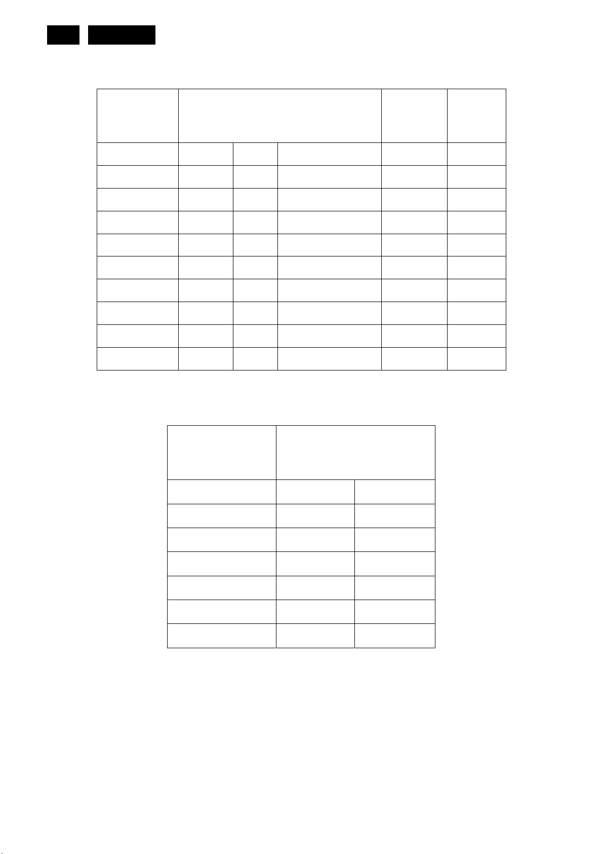
4.2 Factory Preset Display Modes................................16
4.3 Pixel Defect Policy……………………………………17
4.4 Failure Mode of Panel …………………………….…19
5. Block Diagram……………………………................20
5.1 Software Flow Chart............................………….....20
5.2 Electrical Block Diagram.....................……….........22
6. Schematic Diagram............................................... 24
6.1 Scaler Board………………….…………..…………24
6.2 Power Board..........................................................…...38
6.3 IR Board…….………………………..…………………40
6.4 Key Board…….………………………..…………………41
7. PCB Layout………………………………………………...42
7.1 Scaler Board……………………………………………..42
7.2 Power Board……………………………………………44
7.3 IR Board………...………………………………………46
7.4 Key Board………...………………………………………46
8. Wiring Diagram……………………………………….…..47
9. Scaler Board Overview………………………………....48
10. Mechanical Instructions………………………………....49
11. Trouble Shooting…….…….……………………………52
12. ISP Instructions...….....................................................55
13. White Balance, Luminance Adjustment……............56
14. Monitor Exploded View….............................................57
15. Recommended & Spare Parts List...……...................58
16. Different Parts List………………………………………60
17. General Product Specification……………….……….61
SAFETY NOTICE
ANY PERSON ATTEMPTING TO SERVICE THIS CHASSIS MUST FAMILIARIZE HIMSELF WITH THE
CHASSIS AND BE AWARE OF THE NECESSARY SAFETY PRECAUTIONS TO BE USED WHEN
SERVICING ELECTRONIC EQUIPMENT CONTAINING HIGH VOLTAGES.
CAUTION: USE A SEPARATE ISOLATION TRANSFOMER FOR THIS UNIT WHEN SERVICING
REFER TO BACK COVER FOR IMPORTANT SAFETY GUIDELINES
Copyright 2009 Philips Consumer Lifestyle Subject to modification ○K Aug, 20, 2009

2
Meridian 1
Revision List
Version Release Date Revision History
A00 Aug, 20,2009 Initial release, Draft Version

Meridian 1
3
Important Safety Notice
Read and understand all instructions before you use your TV. If damage is caused by failure to follow instructions,
the warranty does not apply.
Safety
y Risk of electric shock or fire!
¾ Never expose the TV to rain or water. Never place liquid containers. Such as vases, near the TV. If liquids
are spilt on or into the TV, disconnect the TV from the power outlet immediately. Contact Philips Consumer
Care to have the TV checked before use.
¾ Never place the TV, remote control or batteries near naked flames or other heat source, including direct
sunlight. To prevent the spread of fire, keep candles or other flames away from the TV, remote control and
batteries at all time.
¾ Never insert objects into the ventilation slots or other openings on the TV.
¾ When the TV is swiveled ensure that no strain is exerted on the power cord. Strain on the power cord can
loosen connections and cause arcing.
y Risk of short circuit or fire!
¾ Never expose the remote control or batteries to rain, water or excessive heat.
¾ Avoid force coming onto power plugs. Loose power plugs can cause arcing or fire.
y Risk of injury or damage to the TV!
¾ Two people are required to lift and carry a TV that weights more than 25 kg.
¾ When stand mounting the TV, use only the supplied stand. Secure the stand to the TV tightly. Place the TV
on a flat, level surface that can support the combined weight of the TV and stand.
¾ When wall mounting the TV, use only a wall mount that can support the weight of the TV. Secure the wall
mount to a wall can support the combined weight of the TV and wall mount. Koninklijke Philips Electronics
N.V. bears on responsibility for improper wall mounting that result in accident, injury or damage.
y Risk of injury to children! Follow these precautions to prevent the TV from toppling over and causing injury to
children:
¾ Never place the TV on a surface covered by a cloth or other material that can be pulled away.
¾ Ensure that no part of the TV hangs over the edge of the surface.
¾ Never place the TV on tall furniture (such as a bookcase) without anchoring both the furniture and TV to the
wall or a suitable support
¾ Educate children about the dangers of climbing on furniture to reach the TV.
y Risk of overheating! Never install the TV in a confined space. Always leave a space of at least 4 inches around
the TV for ventilation. Ensure curtains or other objects never cover the ventilation slots on the TV.
y Risk of damage to the TV! Before you connect the TV to the power outlet, ensure that the power voltage
matches the value printed on the back of the TV. Never connect the TV to the power outlet if the voltage is
different.
y Risk of injury, fire or power cord damage! Never place the TV or any objects on the power cord.

4
y To easily disconnect the TV power cord from the power outlet, ensure that you have full access to the power
cord at all times.
y When you disconnect the power cord, always pull the plug, never the cable.
y Disconnect the TV from the power outlet and aerial before lightning storms. During lightning storms, never touch
any part of the TV, power cord or aerial cable.
y Risk of hearing damage! Avoid using earphones or headphones at high volumes or for prolonged periods of
time.
y If the TV is transported in temperatures below 5℃, unpack the TV and wait until the TV temperature matches
room temperature before connecting the TV to the power outlet.
Meridian 1
Screen Care
y Avoid stationary images as much as possible. Stationary images are images that remain on-screen for
extended periods of time. Examples include: on-screen menus, black bars and time displays. If you must use
stationary images, reduce screen contrast and brightness to avoid screen damage.
y Unplug the TV before cleaning.
y Clean the TV and frame with a soft, damp cloth. Never use substances such as alcohol, chemicals or household
cleaners on the TV.
y Risk of damage to the TV screen! Never touch, push, rub or strike the screen with any object.
y To avoid deformations and color fading, wipe off water drops as soon as possible.
Recycling
Your product is designed and manufactured with high quality materials and components, which can be recycled
and reused. When you see the crossed-out wheeled bin symbol attached to a product, it means the product is
covered by the European Directive 2002/96/EC:
Never dispose of your product with other household waste. Please inform yourself about the local rules on the
separate collection of electrical and electronic products. The correct disposal of your old product helps prevent
potentially negative consequences for the environment and human health.
Your product contains batteries covered by the European Directive 2006/66/EC, which cannot be disposed of with
normal household waste.
Please inform yourself about the local rules on the separate collection of batteries. The correct disposal of batteries
helps prevent potentially negative consequences for the environment and human health.
The most updated user manual on line
The contents of the user manual are subject to change. Please refer to www.philips.com/support for the most
updated user manual info reference.

1. General Specifications
Model 231T1
Meridian 1
5
Picture /
Display
Sound Output (RMS Watts) 2 x 5Wrms, with T.H.D. <10%
Sound Mode Dual, Mono, Stereo, SAP (Secondary Audio Program)
Picture Formats Normal (4:3), Zoom1 (Movie Expand 14:9), Zoom2 (Movie Expand 16:9),
Smart Mode Personal, Vivid, Standard, Movie, Power saver
Rear Connectors Component video in and audio L/R in (YPbPr)
Aspect Ratio 16:9
Resolution
1920 x 1080 @ 60Hz
Super Zoom, Subtitle Zoom, Wide and Auto
SCART1 input / output (CVBS in/out, RGB in, S-Video in, Audio L/R in/out)
SPDIF (digital audio) output
Coaxial aerial I/P (TV input) – Europe type (75 Ω)
PC VGA in (D-SUB)
PC audio in
HDMI 1 in (TV digital interface support HDCP) with digital audio or with PC
audio jack
RS232 connector (for service)
Video out (TV output with audio line out)
Side Connectors CVBS in (cinch)
Audio L/R in (cinch)
CI slot input: PCMCIA card (5V)
USB 4-pin Type-A connector for SW update (only use flash drive)
Power Consumption 45W (typ.)
Off mode power < 0.5W
Mains Power
Ambient temperature
90~264V AC, 50/60 Hz ± 3 Hz
0°C ~40 °C

6
Meridian 1
Tuner / Reception /
Transmissions
Note: Product information is subject to change without notice. For detailed product information, go to
www.philips.com/support
.
Input impedance: 75 Ohm
DVT: DVB- T MPEG4
TV system: PAL B/G D/K I, SECAM B/G D/K L/L’
Video playback: Multi-system PAL, NTSC
Tuner Bandwidth: 7MHz and 8MHz
A
Meridian 1
7
2. TV Monitor Description
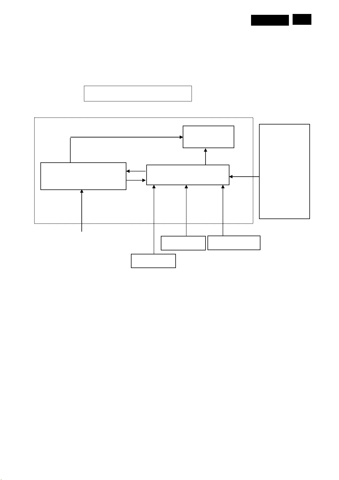
The TV monitor will contain a scaler board, a power board, an IR board and a key board. The scaler board houses
the flat panel control logic, brightness control logic and DDC.
The power board will provide AC to DC Inverter voltage to drive the backlight of panel and the scaler board chips
each voltage.
TV Monitor Block Diagram
CCFL Drive.
Flat Panel and
CCFL backlight
(Include: Adapter, Inverter)
Power Board
Scaler Board
AV Signal, DDC
AC-IN
100V-240V
Key Board
HOST Computer
CVI
USB
HDMI
SPDIF
RS232
VIDEO
TUNER
SCART
PC VGA/
UDIO
IR Board
8
Meridian 1
3. Operating Instructions
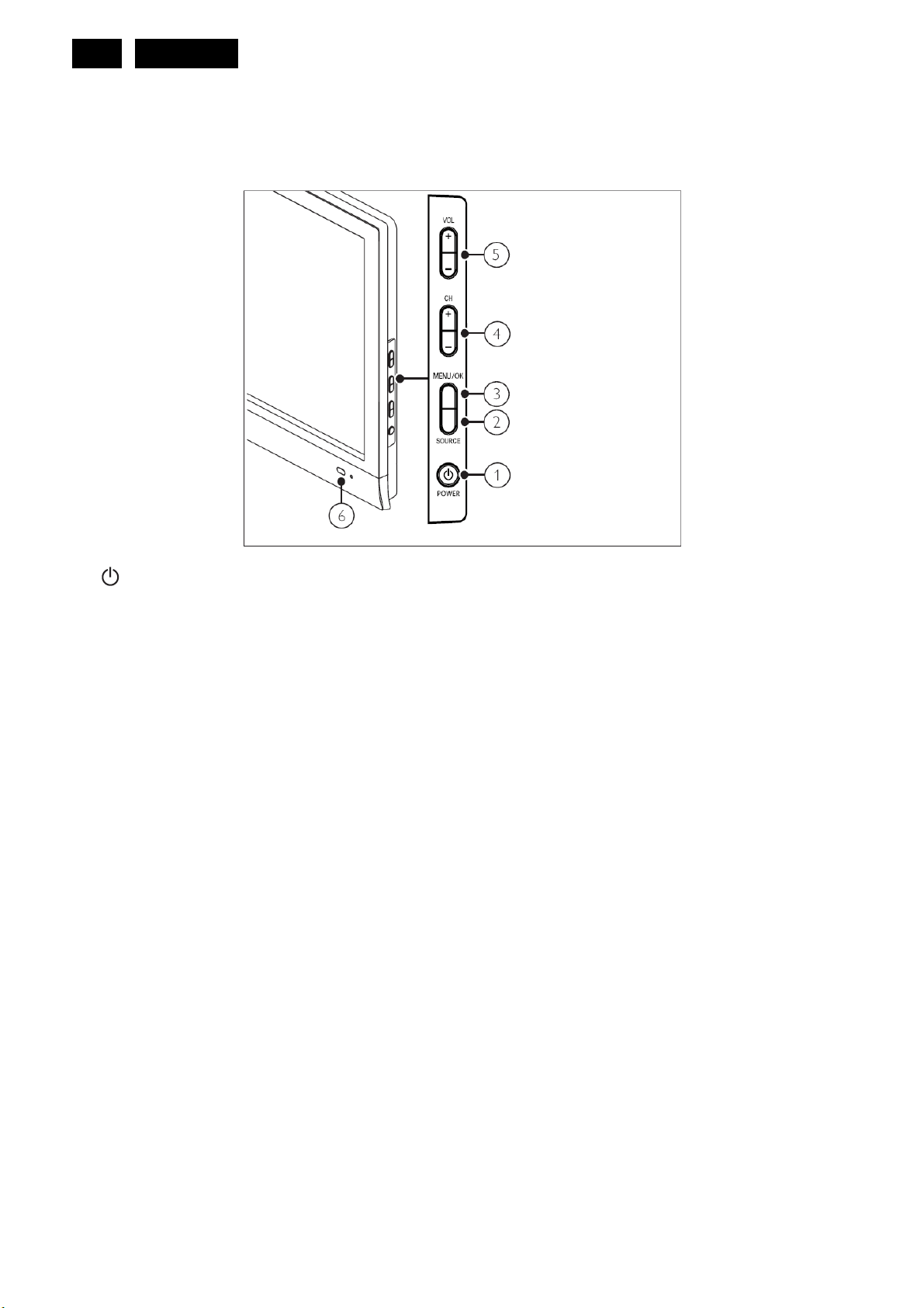
3.1 Front and side controls
Side Controls and indicators
1.
2. SOURCE: Selects connected devices.
3. MENU/OK: Displays the on-screen menu and confirms a selection in menus.
4. CH +/-: Switches to the next or previous channel.
5. VOL+/-: Increases or decreases volume.
6. Power indicator: Red LED: In standby mode or off. Green LED: Power on.
POWER: Switches the TV on or off. The TV is not powered off completely unless it is physically unplugged.
3.2 Remote Control
Meridian 1
9

10
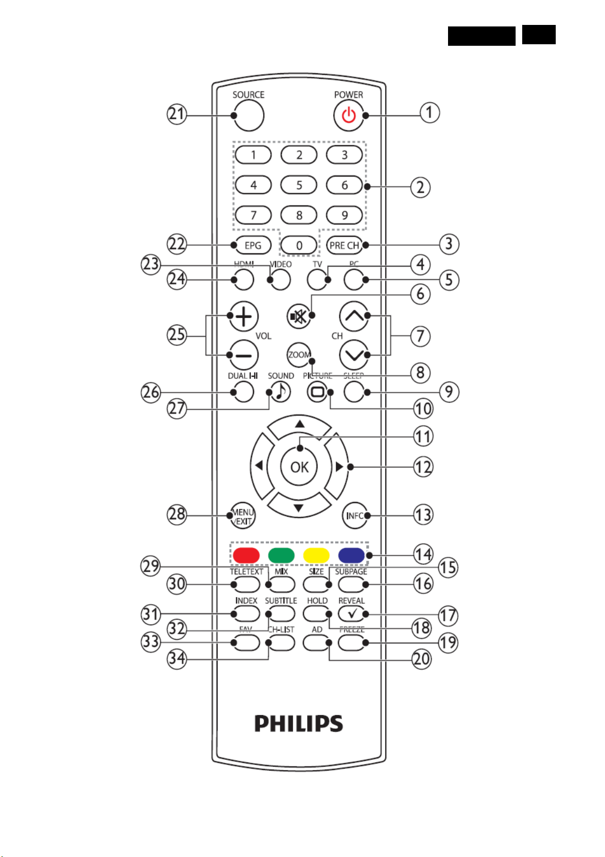
1. (Standby-On): Switch the TV to standby if the TV is on. Switch the TV on if the TV is in standby.
2. 0-9 (Numeric buttons): Select a channel or setting.
3. PRE CH: Return to the previously viewed channel.
4. TV. Press to choose TV mode.
5. PC. Press to choose PC mode.
Meridian 1
6.
7. CH Λ / V (Channel Λ / V): Switch to the next or previous channel.
8. ZOOM: Toggle among screen formats.
9. SLEEP: Toggle to select the preset time to switch the TV to standby mode automatically.
10.
11. OK: Confirm an entry or selection and display the channel grid, when watching TV.
12. ▲ ▼ ◄ ► (Navigation buttons): Navigate through the menus.
13. INFO: Display or hide the information screen about the selected channel.
14. Color buttons: Select tasks or options.
15. SIZE: Toggle to change the font size in Teletext mode. (Full screen / Top half / Bottom half)
16. SUBPAGE: Display the sub page when the Teletext information has more than one page.
17. REVEAL: Reveal hidden information of Teletext.
18. HOLD: Toggle to stop the scrolling of pages to stop the text decoder receiving data.
19. FREEZE: Press to freeze the TV picture.
20. AD (Audio Description) (For RF Digital TV only): UK only: Enables audio commentary for the visually
21. SOURCE: Select connected devices.
(Mute): Switch the sound on or off.
PICTURE: Toggle to select the Smart Picture setting.
handicapped.
22. EPG; Switch the Electronic Program Guide On or Off.
23. VIDEO: Press to switch to VIDEO YPbPr /Composite /SCART mode.
24. HDMI: Press to switch to HDMI mode.
25. VOL +/-: Increase or decrease the volume.
26. DUAL I-II: Toggle to select mono / stereo / dual I/dual II from TV RF input.
27.
SOUND: Toggle to select the Smartsound Mode.
28. MENU/EXIT: Press to open or close the on-screen menu.
29. MIX: Press to overlay the Teletext page on the TV picture.
30. TELETEXT: Press to open or close the Teletext.
31. INDEX: Press to display the index page of Teletext.
32. SUBTITLE: In TV mode: Press to turn the subtitle on or off. In Text mode: Press to open the subtitle page.
33. FAV: Press to display the Favorite List.
34. CH-LIST: Press to display the Channel List.
3.3 Connection overview
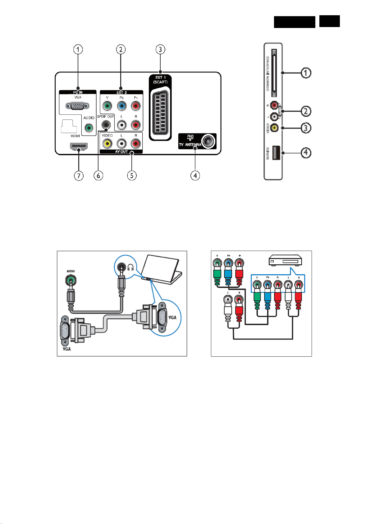
Rear Connectors
Meridian 1
11
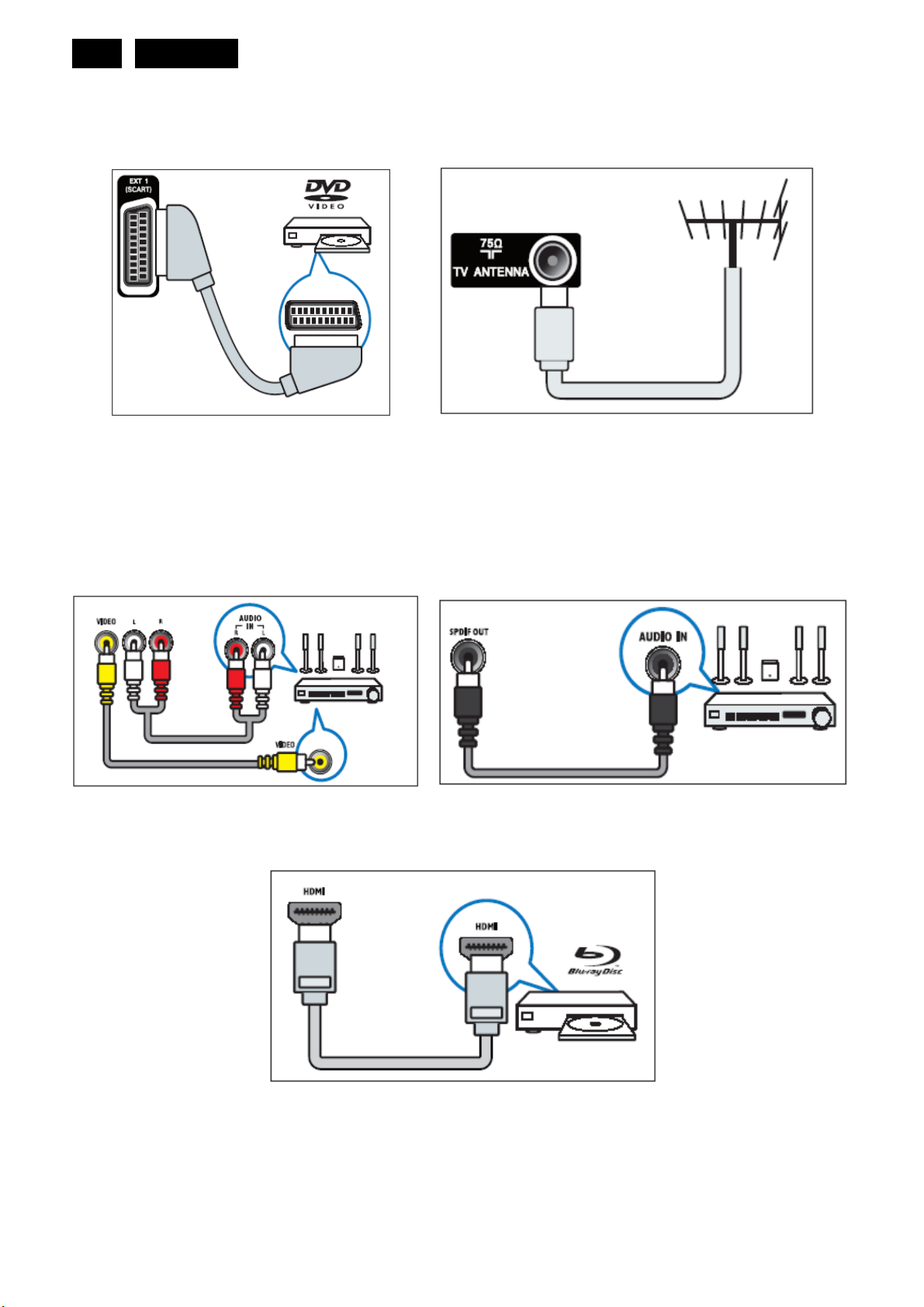
1. PC IN: Audio and video input from a computer. (see Fig-1)
2. EXT 2 (Y PbPr and AUDIO L/R): Analogue audio and video input from analogue or digital devices such as
DVD players or game consoles. (see Fig-2)
Fig- 1 Fig- 2
12
3. EXT 1 (SCART): Analogue audio and video input from analogue or digital devices such as DVD players or
4. TV ANTENNA: Signal input from an antenna, cable or satellite (see Fig-4)
Meridian 1
game consoles. (see Fig-3)
Fig- 3 Fig- 4
5. AV OUT (VIDEO OUT and AUDIO OUT L/R): Audio and video output to analogue devices such as another TV
or a recording device (see Fig-5)
6. SPDIF OUT: Digital audio output to home theatres and other digital audio systems(see Fig-6)
Fig- 5 Fig- 6
7. HDMI:
Digital audio and video input from high-definition digital devices such as Blu-ray players (see Fig-7)
Fig- 7
Side connectors
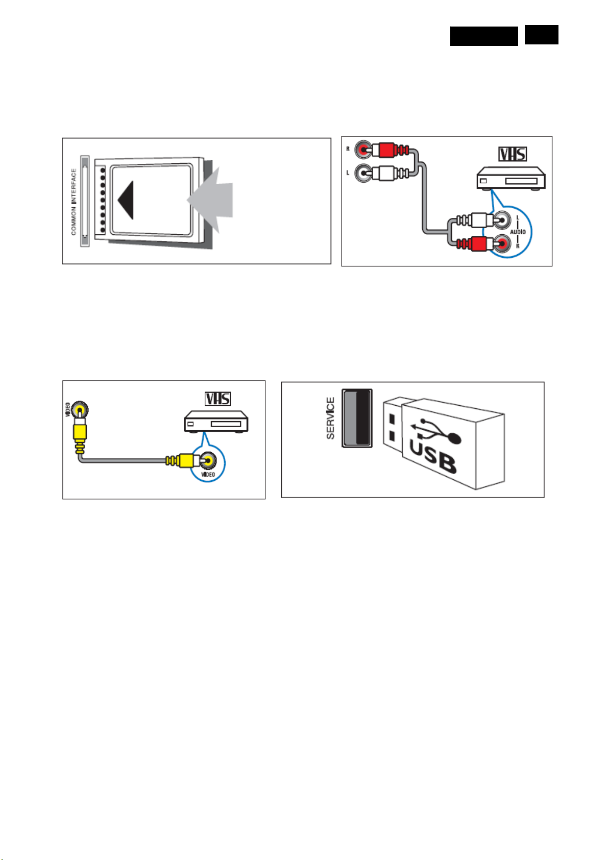
1. COMMON INTERFACE: Slot for a Conditional Access Module (CAM). (see Fig-8)
2. AUDIO L/R: Audio input from analogue devices connected to VIDEO. (see Fig-9)
Meridian 1
Fig- 8 Fig- 9
3. VIDEO: Composite video input from analogue devices such as VCRs. (see Fig-10)
13
4. SERVICE: USB port, for upgrade firmware purpose only. (see Fig-11)
Fig- 10 Fig- 11
14
Meridian 1
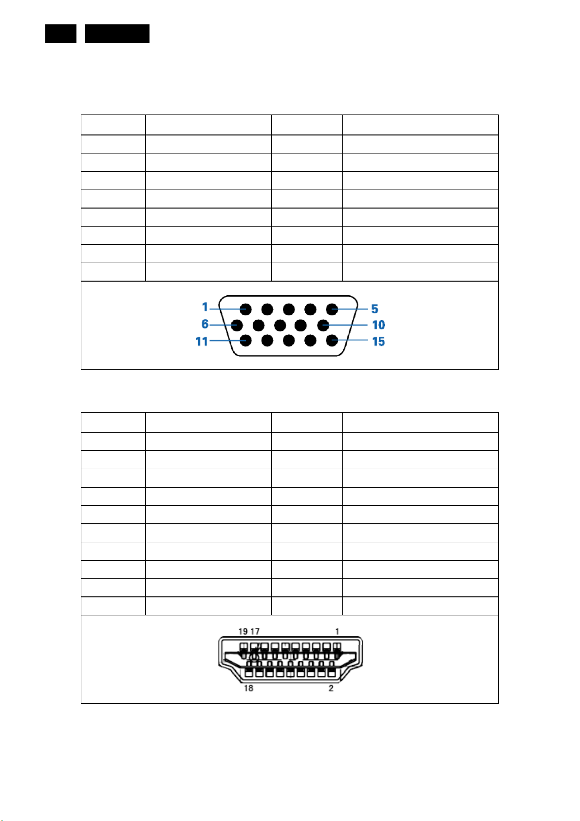
4. Input/ Output Specification
4.1 Input Signal Connector
Analog Connectors
Pin No. Description Pin No. Description
1
2
3
4
5
6
7
8
HDMI Connectors
Pin No. Description Pin No. Description
Red
Green
Blue
NC
GND
Red GND
Green GND
Blue GND
9
10
11
12
13
14
15
+5V (Supply from PC)
Sync GND
NC
Bi-directional data(SDA)
H-sync
V-s ync
Data clock(SCL)
1
2
3
4
5
6
7
8
9
10
TMDS Data2+
TMDS Data2 shield
TDMS Data2-
TMDS Data1+
TMDS Data1 shield
TMDS Data1-
TMDS Data0+
TMDS Data0 shield
TMDS Data0-
TMDS Clock+
11
12
13
14
15
16
17
18
19
TMDS Clock Shield
TMDS Clock-
CEC
Reserved (NC on device)
SCL
SDA
DDC/CEC Ground
+5V Power
Hot Plug Detect
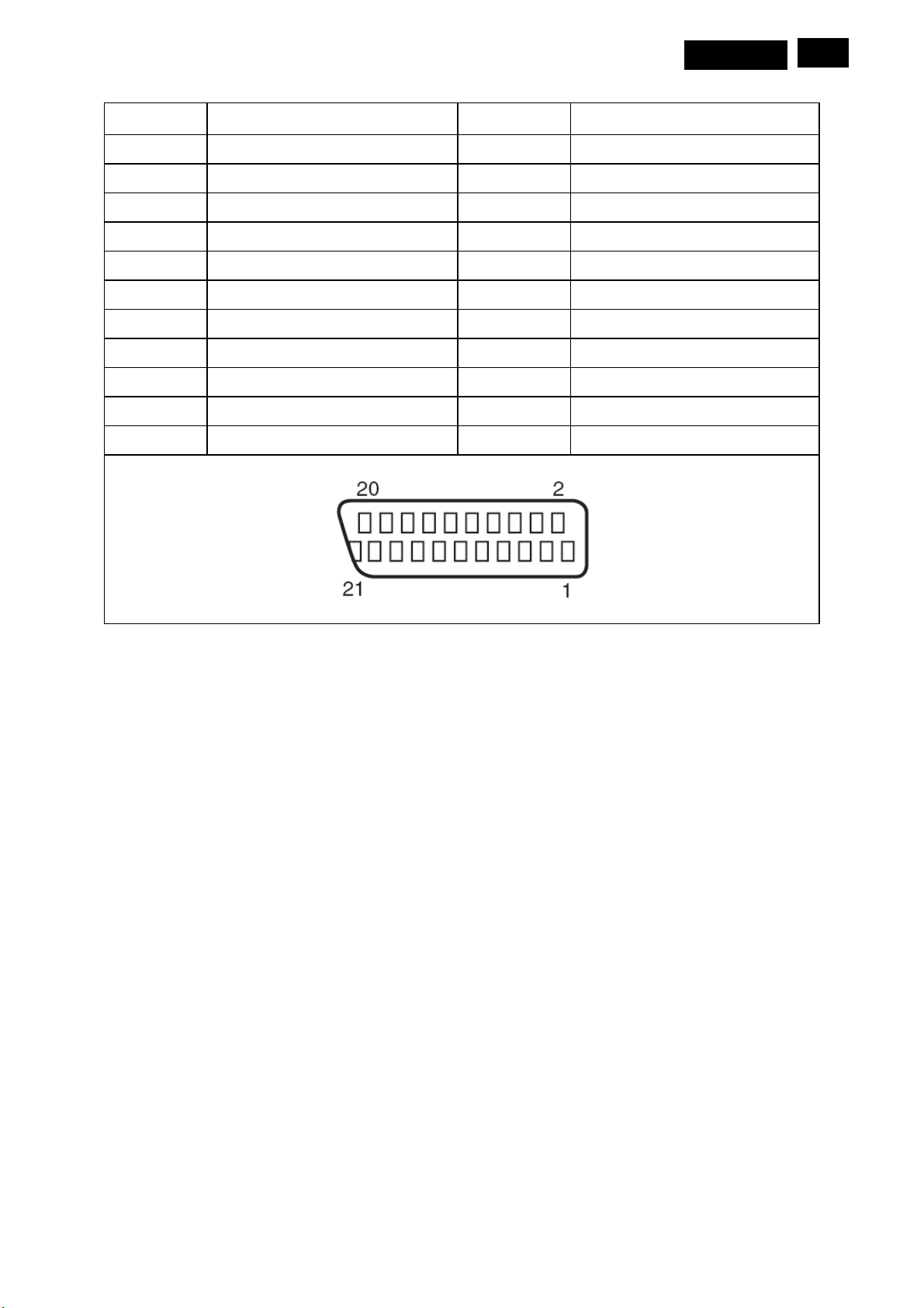
Full SCART Connectors
Pin No. Description Pin No. Description
Meridian 1
15
1
2
3
4
5
6
7
8
9
10
11
Audio output right
Audio input right
Audio output left
GND (audio)
GND (blue)
Audio input left
Blue input
Switch signal input (fast Blanking)
GND (green)
N.C.
Green input
12
13
14
15
16
17
18
19
20
21
N.C.
GND (red)
GND (blanking)
Red input
RGB switching control
GND (video input & output)
GND (RGB switching control)
Video output (composite)
Video input (composite)
Common ground
16
Meridian 1
4.2 Factory Preset Modes
Computer Formats
Factory Preset
Video Formats:
Timing
Resolution
* DMT 4:3 640x480/60 31.47 59.94
* DMT 4:3 640x480/75 37.50 75.00
* DMT 4:3 800x600/60 37.88 60.32
* DMT 4:3 800x600/75 46.88 75.00
* DMT 4:3 1024x768/60 48.36 60.00
* DMT 4:3 1024x768/75 60.02 75.03
* DMT 5:4 1280x1024/60 63.89 60.02
* CVT 1440x900/60 55.94 59.89
* CVT 16:10 1680x1050/60 65.29 59.95
* CVT 16:9 1920x1080/60_RB 67.50 60.00
Horizontal
( KHz )
Vertical
( Hz )
Support Timing Resolution
* 60Hz 480i
* 60Hz 480p
* 50Hz 576i
* 50Hz 576p
* 50Hz, 60Hz 720p
* 50Hz, 60Hz 1080i
* 50Hz, 60Hz 1080p
Meridian 1
17
4.3 Pixel Defect Policy
Philips strives to deliver the highest quality products. We use some of the industry’s most advanced manufacturing
process and practice stringent quality control. However, pixel or sub pixel defects on the TFT LCD panels used in
flat panel monitors are sometimes unavoidable. No manufacturer can guarantee that panels will be free from pixel
defects, but Philips guarantees that any monitor with an unacceptable number of defects will be repaired or
replaced under warranty. This notice explains the different types of pixel defects and defines acceptable defect
levels for each type. In order to qualify for repair or replacement under warranty, the number of pixel defects on a
TFT LCD panel must exceed these acceptable levels. For example, no more than 0.0004% of the sub pixels on a
19” XGA monitor may be defective. Furthermore, Philips sets even higher quality standard for certain types or
combinations of pixel defects that are more noticeable than others. This policy is valid worldwide.
subpixel
subpixel
subpixel
R G B
R G B
Pixels and Sub pixels
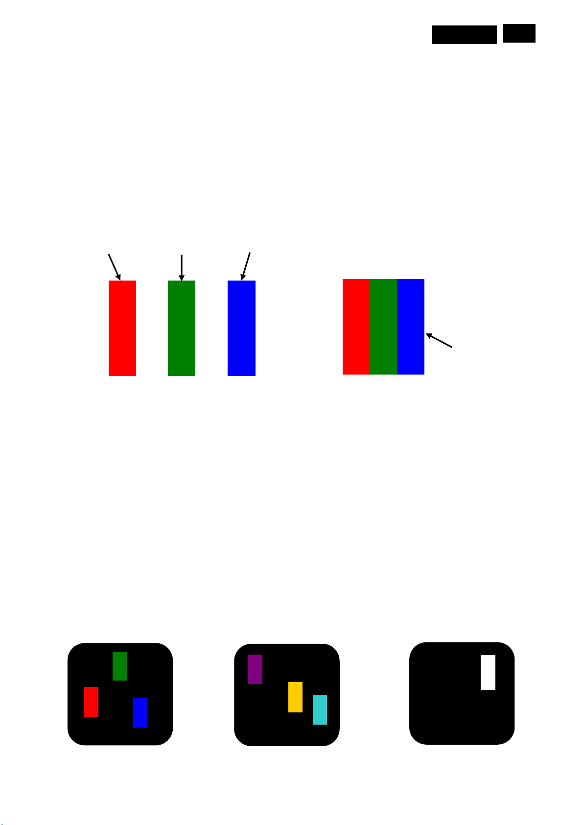
A pixel, or picture element, is composed of three sub pixels in the primary colors of red, green and blue. Many
pixels together form an image. When all sub pixels of pixel are lit, the three colored sub pixels together appear as a
single white pixel. When all are dark, the three colored sub pixels together appear as a signal black pixel. Other
combinations of lit and dark sub appear as single pixels of other colors.
Types of Pixel Defects
Pixel and sub pixel defects appear on the screen in different ways. There are two categories of pixel defects and
several types of sub pixel defects within each category.
Bright Dot Defects Bright dot defects appear as pixels or sub pixels that are always lit or ‘on’. That is, a Bright dot is
a sub-pixel that stands out on the screen when the monitor displays a dark pattern. There are three types of bright
pixel
dot defects:
R
G
B
P
Y
C
W
18
Meridian 1
Two adjacent lit sub pixels:
- Red + Blue = Purple Three adjacent lit sub pixels
(one white pixel) One lit red, green or blue sub pixel - Red + Green = Yellow
- Green + Blue = Cyan (Light Blue)
A red or blue bright dot must be more than 50 percent brighter than neighboring dots while a green
bright dot is 30 percent brighter than neighboring dots.
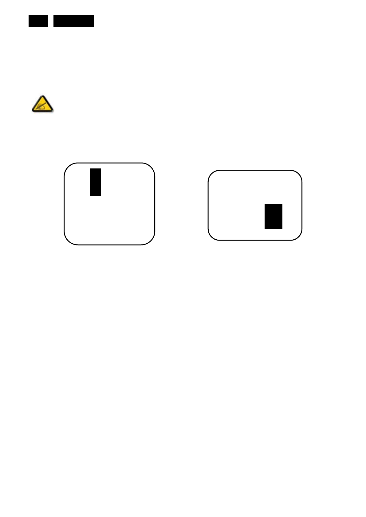
Black Dot Defects Black dot defects appear as pixels or sub pixels that are always dark or ‘off’. That is, a dark dot
is a sub-pixel that stands out on the screen when the monitor displays a light pattern. There are two types of black
dot defects:
One dark sub pixel Two or three adjacent dark sub pixels
Proximity of Pixel Defects
Because pixel and sub pixels defects of the same type that are near to one another may be more noticeable,
Philips also specifies tolerances for the proximity of pixel defects.
Pixel Defect Tolerances
The display does not have more than:
3 bright dots
5 dark dots
5 total bright and dark dots
No more than two adjacent (less than 2.5 mm edge-to-edge) defective pixels.
g
g
g
g
g
4.4 Failure Mode Of Panel
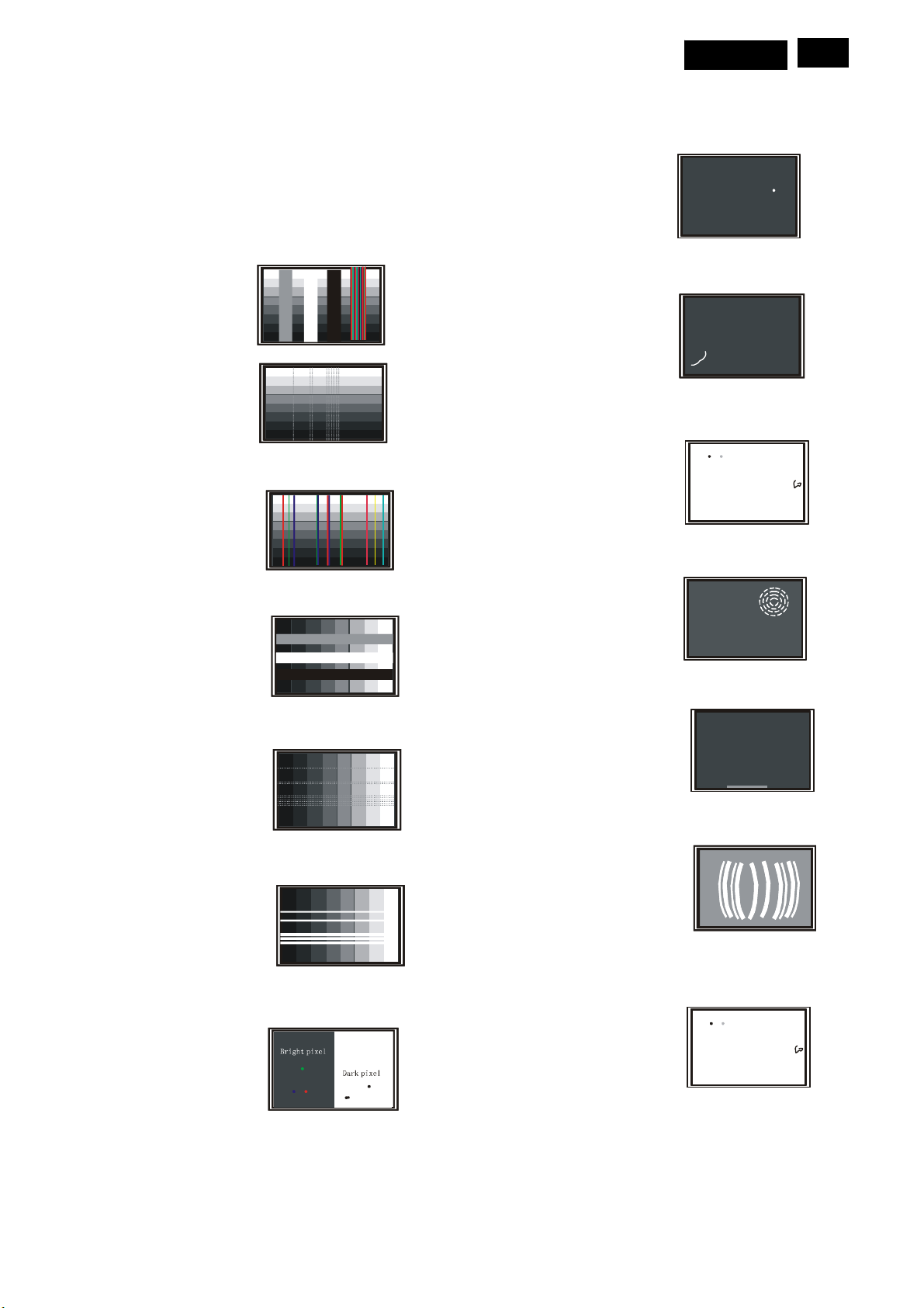
Quick reference for failure mode of LCD panel
e presents problems that could be made by LCD panel.
this pa
It is not necessary to repair circuit board. Simply follow the mechanical
instruction on this manual to eliminate failure by replace LC D panel.
Polarizer has bubbles
Meridian 1
19
Failure description
Vertical block defect
Vertical dim lines
Vertical lines defect
(Always bri
Horizontal block defect
ht or dark)
Phenomenon
Polarizer has bubbles
Foreign material inside
polarizer. It shows liner or
dot shape.
Concentric circle formed
Horizontal dim lines
Horizontal lines defect
(Always bri
Has bri
ht or dark)
ht or dark pixel
Bottom back light of LCD is
brighter than normal
Back light un-uniformity
ht has foreign material.
Backli
Black or white color, liner or
circular type
20
Meridian 1
5. Block Diagram
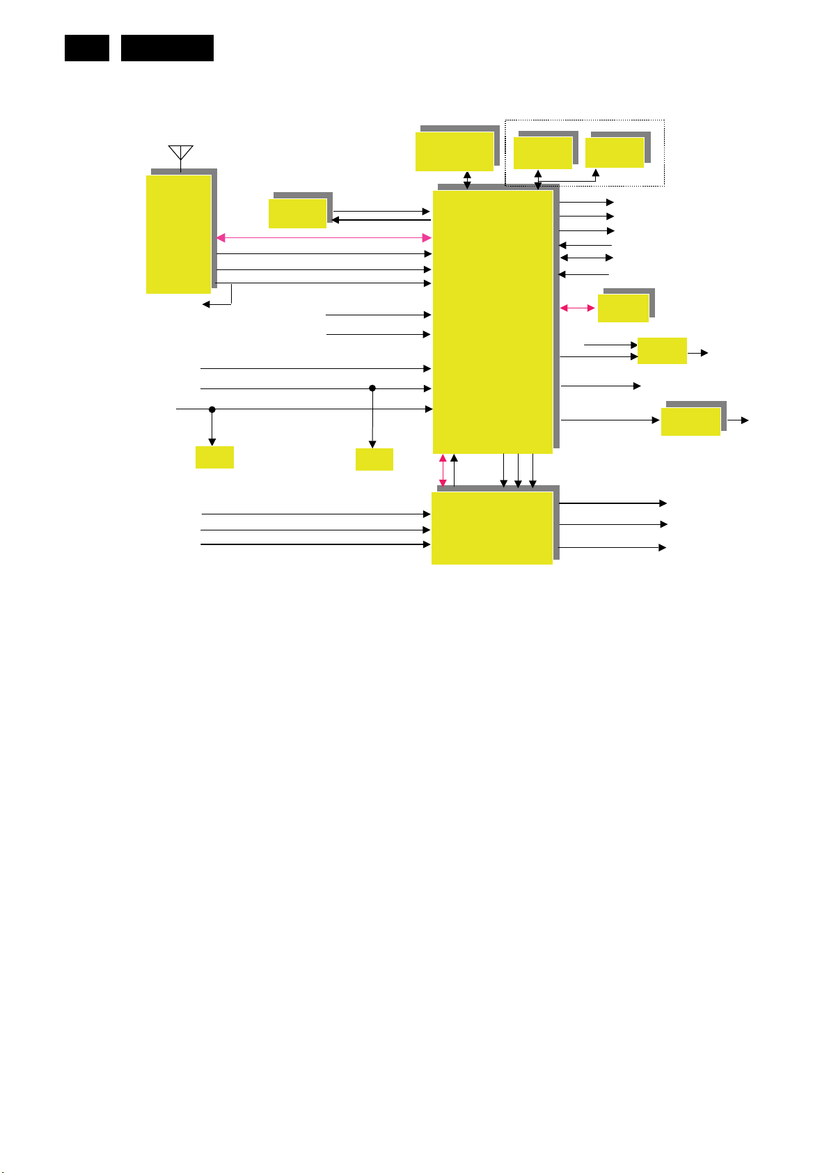
5.1 Software Flow Chat
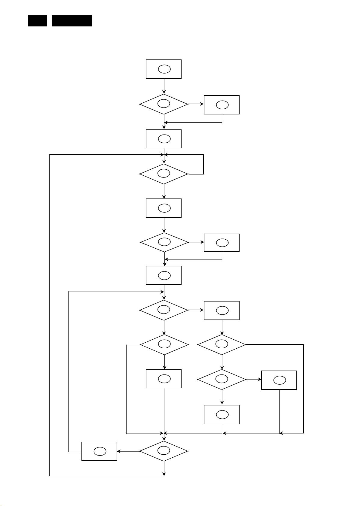
1
2
N
Y
3
4
5
N
Y
6
7
N
Y
9
10
Y
N
12
Y
14
N
13
15
11
17
N
Y
N
Y
16
18
N
19
Y

1) MCU initializes.
2) Is the EPROM blank?
3) Program the EPROM by default values.
4) Get the PWM value of brightness from EPROM.
5) Is the power key pressed?
6) Clear all global flags.
7) Are the AUTO and SELECT keys pressed?
8) Enter factory mode.
9) Save the power key status into EPROM.
Turn on the LED and set it to green color.
Scaler initializes
10) In standby mode?
11) Update the lifetime of back light.
12) Check the analog port, are there any signals coming?
Meridian 1
21
13) Does the Scaler send out an interrupt request?
14) Wake up the Scaler.
15) Are there any signals coming from analog port?
16) Display "No connection Check Signal Cable" message. And go into standby mode after the message
disappears.
17) Program the Scaler to be able to show the coming mode.
18) Process the OSD display.
19) Read the keyboard. Is the power key pressed?
22
Meridian 1
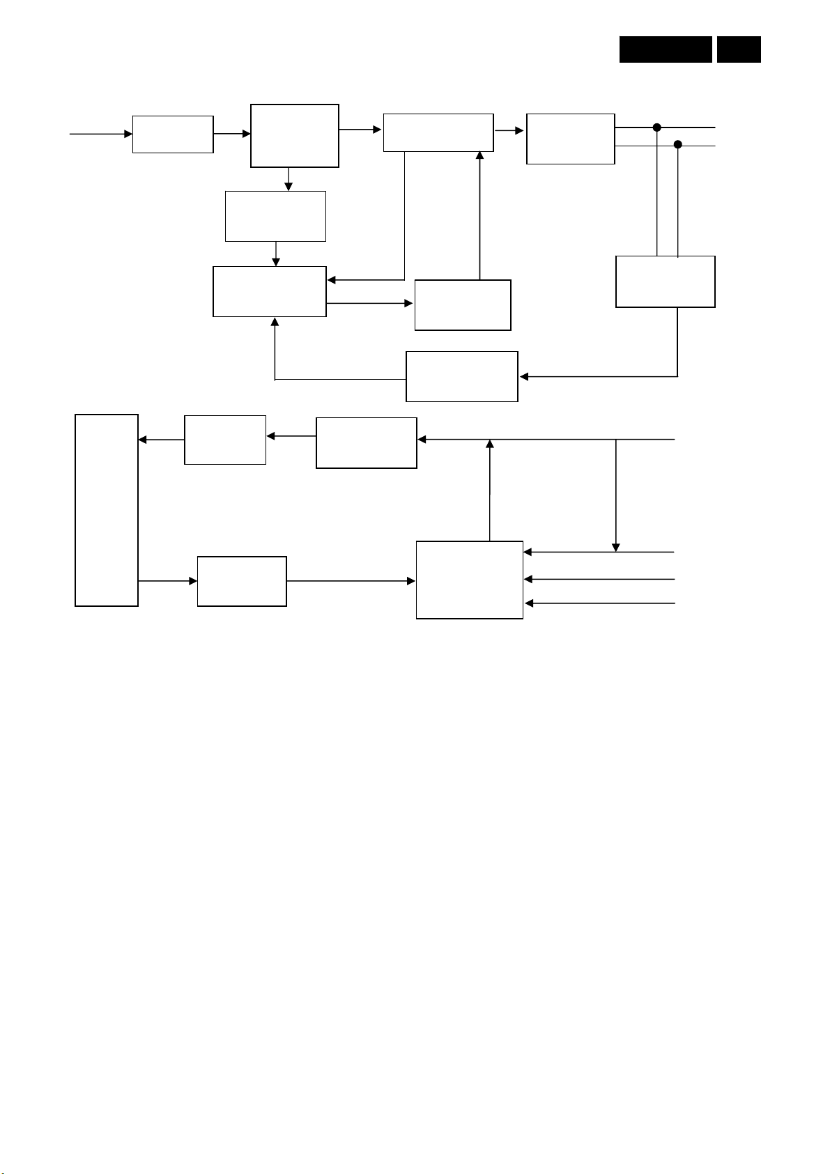
5.2 Electrical Block Diagram
5.2.1 Block diagram
Tuner
ATV CVBS
SCART1 CVI
PC
HDMI-1
Audio R/L of AV CVI
Audio R/L of PC
Audio R/L of Side (CVBS / YC)
DDC
24C02
I2C
IFAT +/-
SIF
CVBS
CVBS / YC x1 (side)
CI system
MT8295
AV CVI x 1
MPEG2 TS
DDC
24C02
DDR2 x 2
32/64Mbyte
MT5362
.MCU
.DTV receiver/demodulator
.MPEG/video/audio decoder
.Scaling
.Video enhancement
.3D comb
.LVDS Transmitter
.HDMI 1.3
.ADC
ADCOUT
I2C
L/R
MT8292
.8 Channel Analog MUX in
.3 L/R line out
.1 Headphone out
NAND Flash
NAND Flash
16MByte
16MByte
I2S
AR/L out X3
NOR Flash
NOR Flash
512K Byte
512K Byte
Keys
I2C
DTV CVBS out
NVM
24C32
ATV CVBS out
USB 2.0
SPDIF Out
LVDS to panel
RC
UART for ISP & Factory alignment
TS5A3157
Analog MUX
Monitor CVBS out
Audio AMP
TDA8933BTW
Line L/R out
Scart l L/R out
Headphone out
t
t
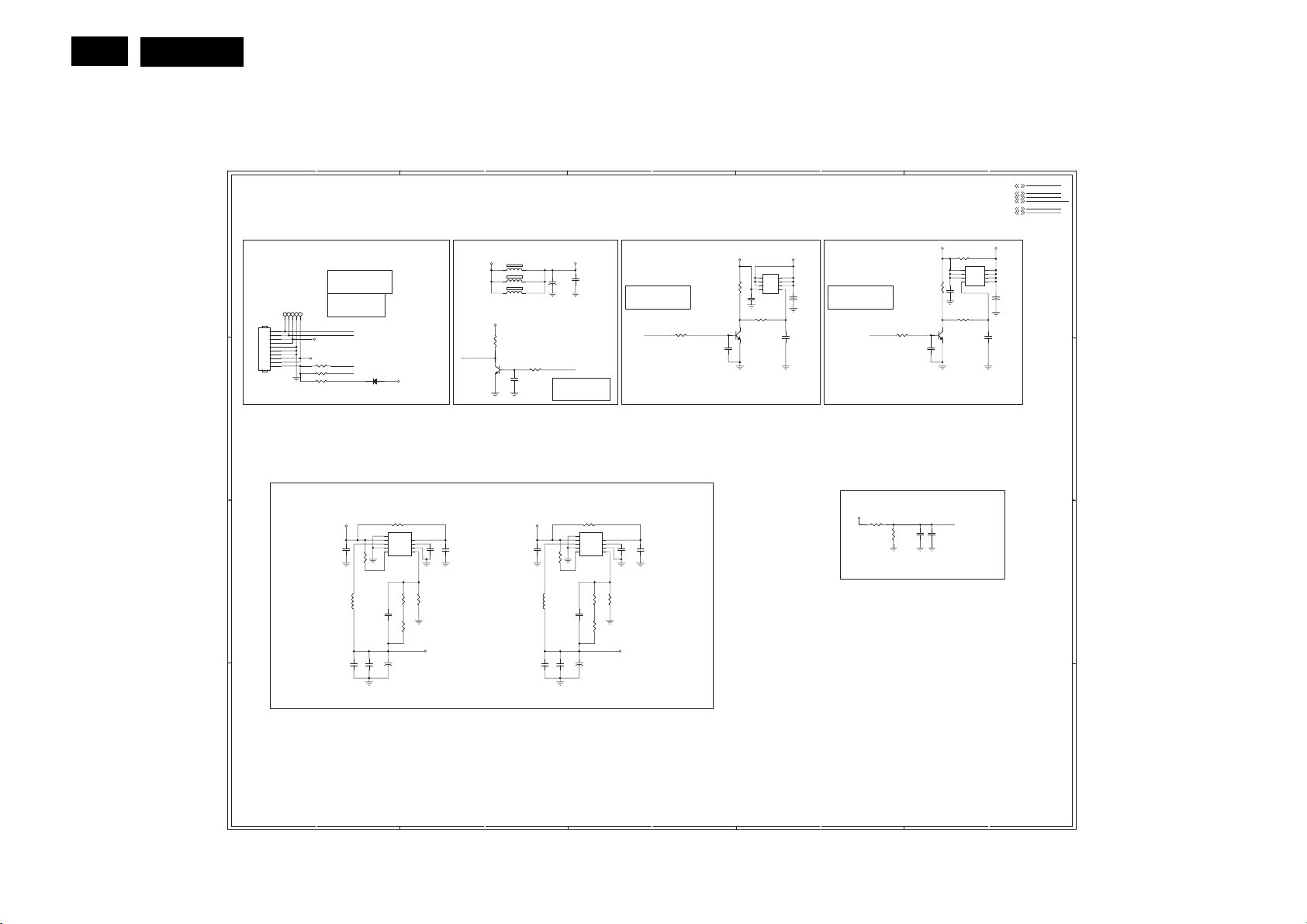
5.2.2 Power / Inverter Board
AC Input
EMI Filter
Start Resistor
(R904, R905)
Bridge
Rectifier
and Filter
Transformer
Meridian 1
Rectifier
Diodes
23
16 V
5 V
Lamp
PWM Control
(IC901)
Output
Circui
Feedback
Circui
Transformer
(PT802)
Power Switch
(Q901)
Photocoupler
(IC903)
PWM Control
OZ9938GN-B
(IC801)
Feedback
Circuit
16 V
5 V
ON/OFF
DIM
24
Meridian 1
6. Schematic
6.1 Scaler Board
715G3292-2
1
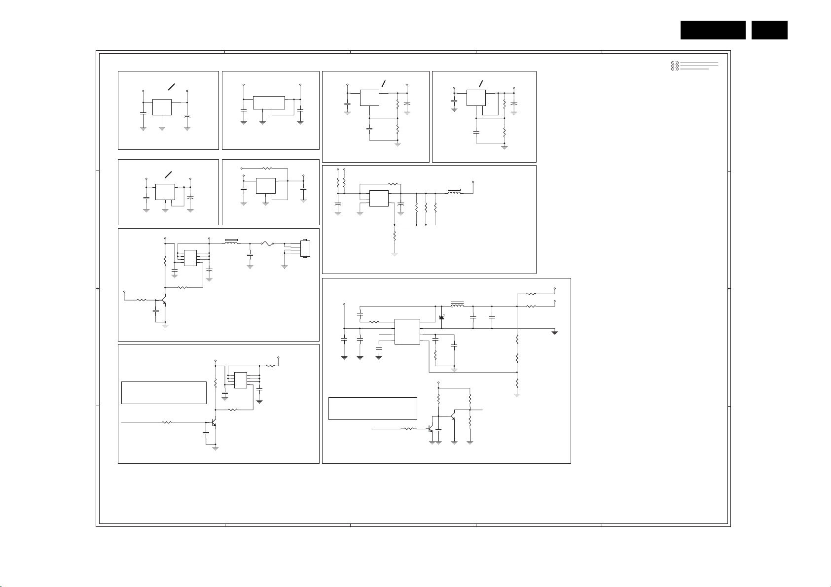
Power 1
A A
DC POWER INPUT
10
9
8
7
6
5
4
3
2
1
CN100
CN100
CONN
CONN
B B
C C
D D
TP104TP104
TP102TP1021TP103TP103
TP105TP105
TP101TP101
1
1
1
1
R113 NC/100 OHM +-5% 1/10WR113 NC/100 OHM +-5% 1/10W
R114 1KOHM +-5% 1/10WR114 1KOHM +-5% 1/10W
R116 100 OHM +-5% 1/10WR116 100 OHM +-5% 1/10W
BRIGHT_ADJ:
Normal:Max:+3V3, Min:0V
Stand_By:0V
INVERTER_ON_OFF:
Normal: High
Stand_By: Low
INVERTER_ON_OFF
BRIGHT_ADJ
+5V
+18V
STANDBY
OPWRSB
D102
D102
2
DV33
A1K
BAS32L
BAS32L
R125
R125
10R 1/8W 5%
R106
R106
L102
L102
4.7uH
4.7uH
10K 1/10W
10K 1/10W
10uF 25V
10uF 25V
10R 1/8W 5%
U103
U103
9
Thermal Pad
8
VIN
7
LX
6
PGND
5
G5627F11U
G5627F11U
C117
C117
+
C111
+
C111
470UF 10V
470UF 10V
1
VCC
2
REF
3
GND
FB4EN
C128
C128
100N 25V
100N 25V
R121
R121
10K1/10W
10K1/10W
R122
R122
3KOHM 1/10W
3KOHM 1/10W
C130
C130
NC/10P 50V
NC/10P 50V
R123
R123
1K 1/10W 1%
1K 1/10W 1%
Vout=0.8 x (1+(1k+3K)/10k) = 1.12V
+5V_SW +5V_SW
C132
C132
10U 16V
10U 16V
C110
C110
10uF 25V
10uF 25V
2
+5V +5V_STB
DV33SB
STANDBY
Q106
Q106
NC/BC847C
NC/BC847C
C104
C104
1uF10V
1uF10V
FB100 120R/3000mAFB100 120R/3000mA
1 2
FB101 120R/3000mAFB101 120R/3000mA
1 2
FB102 NC/120R/3000mAFB102 NC/120R/3000mA
1 2
R144
R144
NC/4K7 1/16W 5%
NC/4K7 1/16W 5%
SMD/0402
C124
C124
NC/100N 16V
NC/100N 16V
SMD/0402
C108
C108
10U 16V
10U 16V
10uF 25V
10uF 25V
R126
R126
NC/10K 1/16W 5%
NC/10K 1/16W 5%
SMD/0402
C116
C116
+
+
C107
C107
470uF 10V
470uF 10V
OPWRSB
OPWRSB:
Normal: High
Stand_by: Low
R109
R109
10K 1/10W
10K 1/10W
L101
L101
4.7uH
4.7uH
C118
C118
10uF 25V
10uF 25V
C134
C134
C106
C106
100N 16V
100N 16V
10R 1/8W 5%
10R 1/8W 5%
U104
U104
9
Thermal Pad
8
VIN
7
LX
6
PGND
5
NC/10P 50V
NC/10P 50V
+
+
R124
R124
G5627F11U
G5627F11U
C112
C112
470UF 10V
470UF 10V
VCC
REF
GND
FB4EN
3
+5V_STB +5V_SW
Q104 SI5441DCQ104 SI5441DC
1
8
D
D
2
7
D
D
3
6
R119 22KOHM +-5% 1/10W R119 22KOHM +-5% 1/10W
D
D
5
2
C121
C121
4.7UF 10V
4.7UF 10V
3
Q101
Q101
BC847C
BC847C
1
C105
C105
100N 16V
100N 16V
R130
R130
1KOHM +-5% 1/10W
1KOHM +-5% 1/10W
G4S
OPWRSB(+5V_SW ON/OFF):
Normal: High
Stand_By: Low
R107
R107
OPWRSB OPWRSB
10KOHM +-5% 1/10W
10KOHM +-5% 1/10W
+5V_STB(+5V1) TO +5V_SW BY OPWRSB
1
2
3
C102
C102
C129
C129
1uF10V
1uF10V
100N 25V
100N 25V
R118
R118
4K7 OHM 1/10W 1%
4K7 OHM 1/10W 1%
R117
R117
3KOHM 1/10W
3KOHM 1/10W
R115
R115
3KOHM 1/10W
3KOHM 1/10W
DV18_DDRDV11
Vout=0.8 x (1+(3K+3K)/4.7k) = 1.82V
+
+
C114
C114
NC/4.7UF 10V
NC/4.7UF 10V
4
OPWRSB(+5V_SW ON/OFF):
C101
C101
Normal: High
330uF 10V
330uF 10V
Stand_By: Low
R108
R108
2
10KOHM +-5% 1/10W
10KOHM +-5% 1/10W
+18V TO +18V_A BY OPWRSB
DV18_DDR
R131 1K 1/10W 1%R131 1K 1/10W 1%
R132
R132
1K1/10W
1K1/10W
MEM_VREF
C120
C120
C119
C119
100N 16V
100N 16V
1uF16V
1uF16V
SMD/0402
DV18_DDR stabilizer
CN100 A1 C101 A4 C102 C3 C103 A5
C104 C2 C105 A4 C106 A3 C107 A2
C108 C2 C109 A5 C110 C1 C111 C1
C112 C3 C114 A4 C115 A5 C116 C2
C117 C1 C118 C2 C119 C5 C120 C5
C121 B3 C122 B5 C124 B2 C128 C2
C129 C3 C130 C1 C132 C1 C134 C3
D102 B1 FB100 A2 FB101 A2 FB102 A2
L101 C2 L102 C1 Q101 A3 Q102 A5
Q104 A4 Q105 A5 Q106 B2 R106 C1
R107 A3 R108 A4 R109 C2 R113 B1
R114 B1 R115 C3 R116 B1 R117 C3
R118 C3 R119 A3 R120 A5 R121 C2
R122 C1 R123 C1 R124 C3 R125 C1
R126 B2 R129 A5 R130 A4 R131 C4
R132 C4 R133 A5 R144 A2 TP101 A1
TP102 A1 TP103 A1 TP104 A1 TP105 A1
5
OPWRSB5
STAND_BY5
BRIGHT_ADJ14
INVERTER_ON_OFF14
MEM_VREF6
+18V_A6
+18V +18V_A
R129
R129
NC/0 OHM +-5% 1/4W
NC/0 OHM +-5% 1/4W
Q105
Q105
1
8
S
D
2
7
S
D
3
6
S
D
4
5
G
D
R120 68KOHM +-5% 1/10W R120 68KOHM +-5% 1/10W
SI4835DDY
SI4835DDY
C109
C109
100N 25V
100N 25V
R133
R133
1KOHM +-5% 1/10W
1KOHM +-5% 1/10W
3
Q102
Q102
BC847C
BC847C
1
C122
C122
4.7UF 10V
4.7UF 10V
+
+
C115
C115
NC/4UF7 25V
NC/4UF7 25V
C103
C103
100uF 25V
100uF 25V
OPWRSB
STAND_BY
BRIGHT_ADJ
INVERTER_ON_OFF
MEM_VREF
+18V_A
1
2
3
4
5
1
Power 2
Add Thermal Pad
+5V_SW
U151
U151
LD1117ADT33TR
LD1117ADT33TR
3
VIN
A A
100N 16V
100N 16V
C166
C166
+5V_SW TO AV33 +5V_STB TO DV33SB
Add Thermal Pad
+5V_SW DV33
C158
C158
100N 16V
100N 16V
+5V_SW TO DV33
B B
+5V_SW
R170
R170
NC/1KOHM +-5% 1/10W
NC/1KOHM +-5% 1/10W
C180
C180
NC/4.7UF 10V
NC/4.7UF 10V
+5V_STB TO DVD_VCC
C C
PANEL_VCC_ON/OFF(PANEL_VCC ON/OFF):
Normal: High
Stand_By: Low
PANEL_VCC_ON/OFF
+5V_STB TO PANEL VCC
AV33
2
VOUT
GND
+
+
C159
C159
/ADJ
/ADJ
100uF 10V
2
GND14
4
Q153 NC/SI5441DCQ153 NC/SI5441DC
8
D
7
D
6
D
5
C182
C182
NC/100N 16V
NC/100N 16V
R169
R169
NC/1KOHM +-5% 1/10W
NC/1KOHM +-5% 1/10W
3
Q154
Q154
NC/BC847C
NC/BC847C
1
100uF 10V
+
+
D
D
D
G4S
C160
C160
100uF 10V
100uF 10V
1
U157 LD1117S33TRU157 LD1117S33TR
VI3VO
+5V_STB DVD_VCC
R171NC/22K 1/10W R171NC/22K 1/10W
2
R158
R158
10KOHM +-5% 1/10W
10KOHM +-5% 1/10W
1
2
3
2
100N 16V
100N 16V
DV18_DDR
100N 16V
100N 16V
SMD/0402
FB150
FB150
1 2
NC/220R/2000mA
NC/220R/2000mA
+
+
C179
C179
NC/100uF 10V
NC/100uF 10V
+5V_STB
R157 22KOHM +-5% 1/10W R157 22KOHM +-5% 1/10W
C113
C113
100N 16V
100N 16V
1KOHM +-5% 1/10W
1KOHM +-5% 1/10W
3
Q151
Q151
MUN2211TIG
MUN2211TIG
1
C156
C156
4.7UF 10V
4.7UF 10V
C151
C151
C173
C173
8
7
6
5
R164
R164
U152
U152
AME8810-AEGTZ 0.6A/3.3V
AME8810-AEGTZ 0.6A/3.3V
3
VIN
R175 NC/0 OHM +-5% 1/10WR175 NC/0 OHM +-5% 1/10W
DV33 DV18_CI
U158 LD1117S18U158 LD1117S18
VI3VO
DV33 TO DV18_CI
F150
F150
NC/1.5A 125V 045101.5MRL
NC/1.5A 125V 045101.5MRL
C183
C183
NC/100N 16V
NC/100N 16V
FOR DVD MODEL
R168
R168
0 OHM +-5% 1/4W
0 OHM +-5% 1/4W
Q150
Q150
SI5441DC
SI5441DC
1
D
D
2
D
D
3
D
D
G4S
VOUT(heat sink)
GND
4
1
4
GND14
4
PANEL_VCC
C167
C167
10uF 16V
10uF 16V
2
2
2
RESERVE
DV33SB+5V_STB
4
3
2
1
10uF 10V
10uF 10V
NC/CONN
NC/CONN
CN150
CN150
C155
C155
C175
C175
10uF 10V
10uF 10V
+5V_SW AV25
C169
C169
100N 16V
100N 16V
SMD/0402
Add Thermal Pad
U153
U153
LD1117ADT-TR
LD1117ADT-TR
3
VIN
VOUT
GND
/ADJ
/ADJ
1
C168
C168
10uF 16V
10uF 16V
2
Vo=1.25 x (1+120R/120R) = 2.5V
+5V_SW TO AV25
+5V_SW
+5V_TU
R178
R178
R177 0 OHM +-5% 1/4WR177 0 OHM +-5% 1/4W
NC/0 OHM +-5% 1/4W
NC/0 OHM +-5% 1/4W
+
+
C177
C177
330UF 16V
330UF 16V
+18V_A
C152
C152
NC/100N 16V
NC/100N 16V
C171
C171
NC/4U7 25V
NC/4U7 25V
PANEL_VCC_ON/OFF(PANEL_VCC ON/OFF):
Normal: High
Stand_By: Low
U159
U159
2
VIN
1
VINH
GND3ADJ
LD39080PT-R
LD39080PT-R
R153
R153
NC/4.7 OHM +-5% 1/10W
NC/4.7 OHM +-5% 1/10W
EN
C172
C172
NC/4U7 25V
NC/4U7 25V
PANEL_VCC_ON/OFF
R180
R180
NC/0 OHM +-5% 1/4W
NC/0 OHM +-5% 1/4W
VO
C170
C170
NC/15N 25V
NC/15N 25V
NC/10KOHM +-5% 1/10W
NC/10KOHM +-5% 1/10W
3
R152 120R 1% 1/10WR152 120R 1% 1/10W
+
+
C161
C161
100N 16V
100N 16V
100uF 10V
100uF 10V
SMD/0402
R151
R151
120R 1% 1/10W
120R 1% 1/10W
Vo=1.25 x (1+1R/120R) = 1.26V
4
5
R174
R174
4K7 OHM 1/10W 1%
4K7 OHM 1/10W 1%
1
BOOT
2
VIN
3
EN
4
SS
NC/TPS54231DR
NC/TPS54231DR
+
+
1%
1%
C178
C178
470UF 10V
470UF 10V
30K 1/10W
30K 1/10W
27K 1/10W 1%
27K 1/10W 1%
R176
R176
R173
R173
R172
R172
NEARLY TUNER
+5V_TUNER FROM Regulator
U155
U155
8
PH
7
GND
6
COMP
C163
C163
5
VSNS
NC/18N 50V
NC/18N 50V
NC/20K 1/10W 1%
NC/20K 1/10W 1%
R154
R154
+18V_A
R167
R167
NC/47KOHM +-5% 1/10W
NC/47KOHM +-5% 1/10W
3
R166
R166
2
NC/4U7 25V
NC/4U7 25V
Q152
Q152
1
NC/BC847C
NC/BC847C
3
LD1117S-TR
LD1117S-TR
10uF 16V
10uF 16V
U154
U154
VIN
C153
C153
Add Thermal Pad
2
VOUT
GND
TH
1
4
AV25 AV12
C164
C164
AV25 TO AV12
+5V_TUNER
FB151
FB151
1 2
220R/2000mA
220R/2000mA
NC/820K 1/10W 1%
NC/820K 1/10W 1%
L150 NC/15uHL150 NC/15uH
ZD150
ZD150
C154
C154
NC/SS2P4
NC/SS2P4
NC/22U 10V
C165
C165
NC/12P 50V
NC/12P 50V
3
NC/BC847C
NC/BC847C
1
NC/22U 10V
R161
R161
NC/330KOHM +-5% 1/10W
NC/330KOHM +-5% 1/10W
EN
R165
R165
NC/82KOHM +-5% 1/10W
NC/82KOHM +-5% 1/10W
1 2
Q155
Q155
2
C174
C174
18V_A TO PANEL_VCC
C157
C157
NC/22U 10V
NC/22U 10V
R162120R 1% 1/10WR162120R 1% 1/10W
+
+
C162
C162
100uF 10V
100uF 10V
R163
R163
1 OHM +-5% 1/10W
1 OHM +-5% 1/10W
R179
R179
NC/0 OHM +-5% 1/4W
NC/0 OHM +-5% 1/4W
R160
R160
NC/0 OHM +-5% 1/4W
NC/0 OHM +-5% 1/4W
R155
R155
NC/560R 1/10W 1%
NC/560R 1/10W 1%
R156
R156
NC/18 KOHM +-1% 1/10W
NC/18 KOHM +-1% 1/10W
R159
R159
NC/3K3 1/10W 1%
NC/3K3 1/10W 1%
4
PANEL_VCC_ON/OFF5
OPWRSB5
+18V_A6
CN150 B2 C113 C1
C151 A2 C152 C3
C153 A3 C154 C3
C155 A2 C156 D1
C157 C4 C158 B1
C159 A1 C160 B1
C161 A3 C162 A4
C163 C3 C164 A3
C165 C3 C166 A1
C167 C2 C168 A3
C169 A2 C170 C3
C171 C2 C172 C3
C173 B2 C174 D3
C175 B2 C177 B2
C178 B3 C179 B1
C180 C1 C182 B1
C183 B2 FB150 B1
FB151 B3 F150 B2
L150 C3 Q150 C2
Q151 D1 Q152 D3
Q153 B1 Q154 C1
Q155 D3 R151 A3
R152 A3 R153 C3
R154 C3 R155 C4
R156 C4 R157 C1
R158 D1 R159 C4
R160 C4 R161 C3
R162 A4 R163 A4
R164 C2 R165 D3
+5V_TU
PANEL_VCC
R166 D3 R167 C3
R168 C2 R169 B1
R170 C1 R171 B1
R172 B3 R173 B3
R174 B3 R175 A2
R176 B3 R177 B2
R178 B2 R179 B4
R180 B3 U151 A1
U152 A2 U153 A3
U154 A3 U155 C3
U157 B1 U158 B2
U159 B3 ZD150 C3
Meridian 1
5
PANEL_VCC_ON/OFF
OPWRSB
+18V_A
25
ONLY PnS MODELONLY Click MODEL
D D
1
2
3
4
5
26
Meridian 1
1
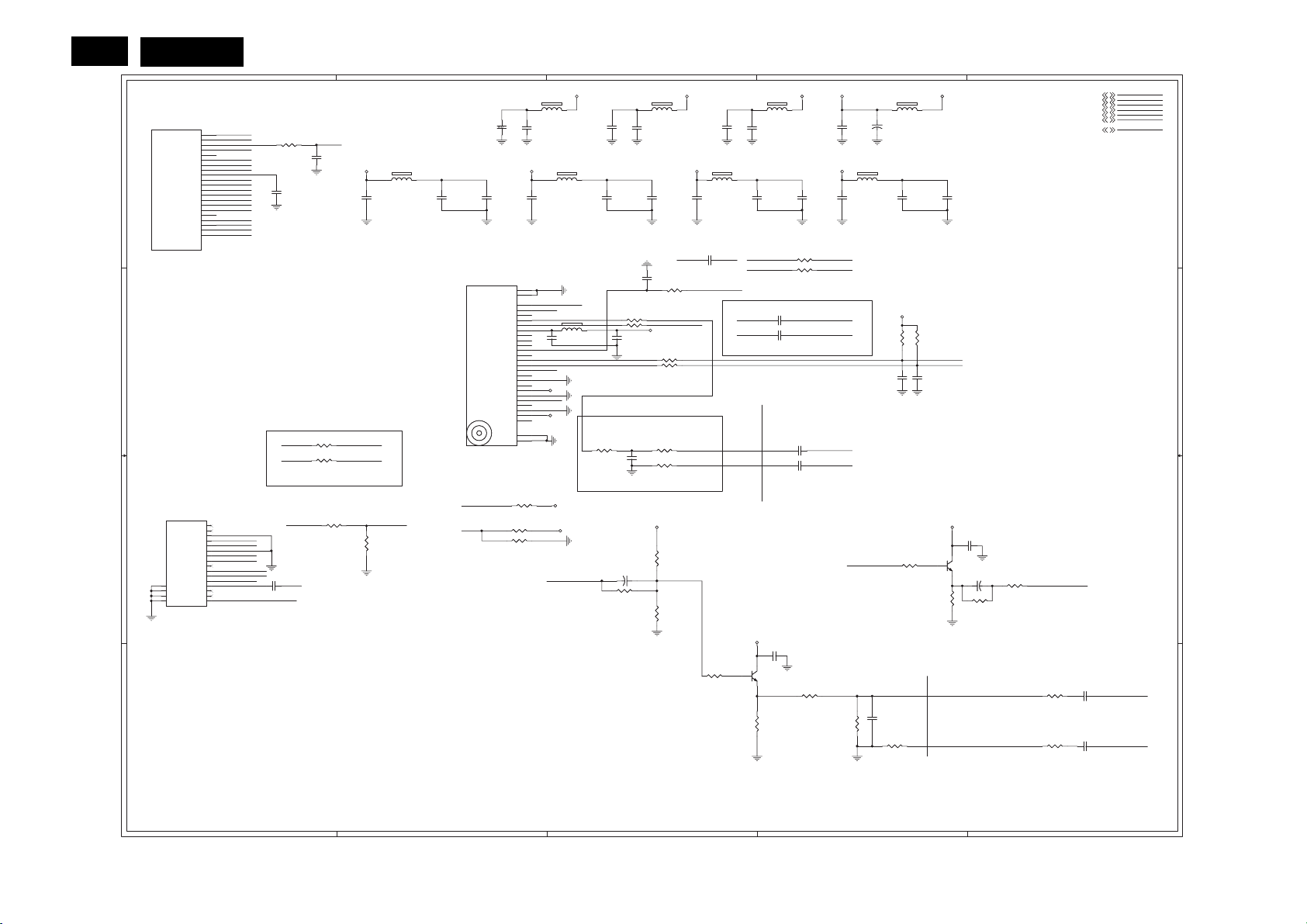
Tuner
U400B
U400B
AVSS33_DIG
AA22
AVSS33_DIG
AVDD33_DIG
TUNER_CLK
TUNER_DATA
A A
DVSS25_IFADC
AVSS25_IFADC
AVSS25_IFADC
AVSS25_REF
DVDD25_IFADC
AVDD25_IFADC
AVDD25_REF
AVSS33_SIF
AVDD33_SIF
MT5362ANG/B
MT5362ANG/B
B B
TU202
TU202
C C
20
TH4
19
TH3
18
TH2
17
TH1
NC/LG TDTW-S710D
C200 C3 C201 A4 C202 A4 C203 C4 C204 B3 C207 B4 C208 C4 C209 D4
C210 D5 C211 D4 C212 A4 C213 A4 C214 A4 C215 A2 C216 A2 C217 A3
C218 A3 C219 A3 C220 A3 C221 D5 C222 C4 C223 B3 C224 B4 C225 B4
C226 B2 C227 B3 C229 A4 C230 A3 C231 A3 C232 A2 C233 A2 C234 A2
C235 A3 C236 A2 C237 A3 C238 A1 C242 B4 C243 B4 C244 A1 C245 A3
C246 C1 FB200 A4 FB201 A4 FB203 A2 FB204 A3 FB205 A4 FB206 B3 FB207 A3
D D
FB208 A2 FB209 A3 Q200 C4 Q201 D3 R200 B3 R201 C3 R202 B3 R203 C3
R204 C4 R205 B3 R206 B3 R207 B4 R209 C2 R210 D4 R211 B4 R212 C1
R213 C3 R214 C4 R215 C3 R216 C4 R217 D3 R218 D5 R219 D3 R220 C5
R221 D4 R222 D4 R223 C2 R224 C2 R225 C2 R227 B3 R228 B3 R230 A4
R231 B1 R232 A4 R233 D5 R234 A1 R235 B1 R236 B3 TU201 B2 TU202 C1
IF_AGC
RF_AGC
VIN_ATV
VIP_ATV
VINDC
SIFP
SIFN
RF AGC
MOPLL AS
NC/TUNER
NC/TUNER
IF AGC
AUDIO
VIDEO
AVDD33_DIG
Y23
IF_AGCT
E24
TUNER_SCL1
F24
E25
TUNER_SDA1
F25
FAT_IN-
R25
FAT_IN+
T25
VINDC
T26
DVSS25_IFADC
V22
AVSS25_IFADC
U23
AVSS25_IFADC
T24
AVSS25_IFADC
P25
DVDD25_IFADC
V23
AVDD25_IFADC
U24
AVDD25_IFADC
P26
AA24
AF
MPX0P
AB25
MPX0N
AB26
AVSS33_SIF
Y22
AVDD33_SIF
W22
R234
R234
10KOHM +-5% 1/10W
10KOHM +-5% 1/10W
C238
C238
100N 16V
100N 16V
SMD/0402
NXP_DIF1_LG
NXP_DIF2_LG
IF_AGC
C244
C244
47N 16V
47N 16V
R235
R235
NC/0 OHM +-5% 1/10W
NC/0 OHM +-5% 1/10W
R231
R231
NC/0 OHM +-5% 1/10W
NC/0 OHM +-5% 1/10W
NXP_DIF1
NXP_DIF2
1 2
C233
C233
NC/1uF/16V
NC/1uF/16V
FB208
FB208
120R/500mA
120R/500mA
Close to NXP tuner
1
NC
2
NC
3
GND
+5V_T3
4
+B
RF_AGC
5
6
GND
SDA
SCL
DIF+
SDA
7
SCL
8
9
NXP_DIF2_LG
10
NXP_DIF1_LG
11
DIF-
IF_AGC#
12
C246
C246
13
SIF
NC
NC/100P 50V
NC/100P 50V
14
SMD
15
16
R212 NC/100K OHM 1/16WR212 NC/100K OHM 1/16W
SIF
TUNER_CVBS
RF_AGC_5362RF_AGC
R209
R209
NC/100K OHM 1/16W
NC/100K OHM 1/16W
2
AVDD25_IFADC
C234
C234
4U7 10V
4U7 10V
AVSS25_IFADC
+5V_T +5V_T+5V_T +5V_T
FB203
FB203
+5V_T2 +5V_T3 +5V_T4
1 2
NC/120R/500mA
NC/120R/500mA
C216
NC/100N 16V
NC/100N 16V
FQD1116ME/BM
FQD1116ME/BM
AS_TUNER
AS_IF
C215
C215
C216
NC/10U 10V
NC/10U 10V
C232
C232
100N 16V
100N 16V
SMD/0402 SMD/0402 SMD/0402 SMD/0402
NC/0R05 1/10W 5%
NC/0R05 1/10W 5%
0 OHM +-5% 1/10W
0 OHM +-5% 1/10W
28
TH4
27
TH3
24
CVBS
23
AS_IF
22
NC
21
SIF2
20
SIF1
19
+5V IF
18
NC
17
DIF2
16
DIF1
15
IF_AGC
14
REF
13
SDA
12
SCL
11
As
10
NC
9
GND
8
VT
7
VP(TUN)
6
GND
5
RF_AGC
4
NC
3
GND
2
Ant Pwr
1
RF_IO
26
TH2
25
TH1
TU201
TU201
R223
R223
NC/0R05 1/10W 5%
NC/0R05 1/10W 5%
R224
R224
R225
R225
C236
C236
NC/1uF/16V
NC/1uF/16V
AS_IF
C226
C226
SDA
SCL
AS_TUNER
RF_AGC
TUNER_CVBS
FB209
FB209
1 2
120R/500mA
120R/500mA
TUNER_CVBS
1 2
FB206
FB206
120R/500mA
120R/500mA
100N 16V
100N 16V
+5V_T3
+5V_T4
+5V_T3
+5V_T2
C217
C217
100N 16V
100N 16V
R236
R236
0 OHM +-5% 1/10W
0 OHM +-5% 1/10W
3
FB204
FB204
1 2
120R/500mA
120R/500mA
C218
C218
10uF 10V
10uF 10V
DVDD25_IFADC
C237
C237
4U7 10V
4U7 10V
DVSS25_IFADC
IF_AGC#
R227 0 OHM +-5% 1/16WR227 0 OHM +-5% 1/16W
R228 0 OHM +-5% 1/16WR228 0 OHM +-5% 1/16W
+5V_TUNER
C227
C227
100N 16V
100N 16V
C219
C219
NC/100N 16V
NC/100N 16V
FB207
FB207
AV33AV25 AV25
1 2
120R/500mA
120R/500mA
C230
C235
C235
100N 16V
100N 16V
10N 50V
10N 50V
C204
C204
R202 4.7KOHM +-5% 1/10WR202 4.7KOHM +-5% 1/10W
R205
R205
200 OHM +-5% 1/10W
200 OHM +-5% 1/10W
R206
R206
200 OHM +-5% 1/10W
200 OHM +-5% 1/10W
C230
NC/1uF/16V
NC/1uF/16V
C245
C245
3P3 50V
3P3 50V
NXP_DIF2 DFAT_IN-
SMD/0402
NXP_DIF1
SMD/0402
FB205
FB205
1 2
NC/120R/500mA
NC/120R/500mA
C220
C220
NC/10U 10V
NC/10U 10V
AVDD33_DIG
C231
C231
4U7 10V
4U7 10V
AVSS33_DIG
SMD/0402
NXP_DIF1NXP_DIF1 NXP_DIF2
R230
R230
0 OHM +-5% 1/16W
0 OHM +-5% 1/16W
NXP_DIF2
R232
R232
0 OHM +-5% 1/16W
0 OHM +-5% 1/16W
IF_AGC
SMD/0402
DFAT_IN+
ROUTE SYMMETRICALLY
C242
C242
10N 16V
10N 16V
C243
C243
10N 16V
10N 16V
C229
C229
100N 16V
100N 16V
Near Tuner NEAR 5362
SIF MPX0_TUN
R200
R200
0 OHM +-5% 1/10W
0 OHM +-5% 1/10W
C223
C223
NC/15P 50V
NC/15P 50V
ROUTE SYMMETRICALLY
+5V_TUNER +5V_TUNER
SMD
C200
C200
47uF 16V
47uF 16V
+
+
R203
R203
NC/0R05 1/10W 5%
NC/0R05 1/10W 5%
R201
R201
0 OHM +-5% 1/10W
0 OHM +-5% 1/10W
R215
R215
10KOHM +-5% 1/10W
10KOHM +-5% 1/10W
ATV_CVBS_OUT
R213
R213
33KOHM +-5% 1/10W
33KOHM +-5% 1/10W
MPX0_GND
R217
R217
10 OHM +-5% 1/10W
10 OHM +-5% 1/10W
75 OHM +-5% 1/10W
75 OHM +-5% 1/10W
+5V_TUNER
R219
R219
C209 100N 16VC209 100N 16V
Q201
Q201
2SD2653K
2SD2653K
AVCVBS0
C207
C207
10N 16V
10N 16V
C208
C208
10N 16V
10N 16V
R221
R221
75 OHM +-5% 1/10W
75 OHM +-5% 1/10W
75 OHM +-5% 1/10W
75 OHM +-5% 1/10W
AV33
DFAT_IN+
DFAT_IN-
FAT_IN+
FAT_IN-
MPX0P
SMD/0402
MPX0N
SMD/0402
C201
C201
100N 16V
100N 16V
FB200
FB200
1 2
120R/500mA
120R/500mA
C213
C213
NC/1uF/16V
NC/1uF/16V
ATV_CVBS_OUT
R222
R222
4
+
+
C202
C202
100uF 16V
100uF 16V
SMD
R207
R207
4.7KOHM +-5% 1/10W
4.7KOHM +-5% 1/10W
C224
C224
100P 50V
100P 50V
10 OHM +-5% 1/10W
10 OHM +-5% 1/10W
Close to
Tuner
C211
C211
47P 50V
47P 50V
0 OHM +-5% 1/10W
0 OHM +-5% 1/10W
FB201
FB201
1 2
220R/2000mA
220R/2000mA
+5V_TUNER
75 OHM +-5% 1/10W
75 OHM +-5% 1/10W
R210
R210
AVDD33_SIF
C214
C214
4U7 10V
4U7 10V
AVSS33_SIF
R214
R214
+5V_TUNER
C212
C212
100N 16V
100N 16V
R211
R211
4.7KOHM +-5% 1/10W
4.7KOHM +-5% 1/10W
TUNER_SDA1
TUNER_SCL1
C225
C225
100P 50V
100P 50V
C203 100N 16VC203 100N 16V
Q200
Q200
2SD2653K
2SD2653K
R216
R216
SCART1 TV BYPASS
C222 NC/470uF 16V
C222 NC/470uF 16V
R204 0 OHM +-5% 1/10WR204 0 OHM +-5% 1/10W
TUNER_CVBSN
R220
R220
+
+
62 OHM 1/10W
62 OHM 1/10W
5
ATV_MUX_IN9
ATV_CVBS_OUT9
CVBS0P10
CVBS0N10
SCT1_AV_OUT9
SCT1_AVO_GND9
RF_AGC_53629
ATV_MUX_IN
Close to
MT5336
R218
R218
100 OHM +-5% 1/16W
100 OHM +-5% 1/16W
SMD/0402
R233
R233
75 OHM +-5% 1/16W
75 OHM +-5% 1/16W
SMD/0402
C210
C210
47N 16V
47N 16V
SMD/0402
C221
C221
1UF 6V3
1UF 6V3
SMD/0402
ATV_MUX_IN
ATV_CVBS_OUT
CVBS0P
CVBS0N
SCT1_AV_OUT
SCT1_AVO_GND
RF_AGC_5362
CVBS0P
CVBS0N
1
2
3
4
5

1
MT5362 BYPASS / TRAP
A A
B B
C C
DV33
D D
TP250TP250
DV33
DV11
POCE0#
PACLE
PAALE
POWE#
PDD6
PDD7
POOE#
PARB#
PDD2
PDD5
PDD4
PDD3
PDD1
POCE1#
1
PDD0
MT5362BMG/BU400F MT5362BMG/BU400F
AC5
VCC3IO
AB6
VCC3IO
B1
DVSS
C2
DVSS
K2
DVSS
U2
DVSS
V2
DVSS
D3
DVSS
L3
DVSS
V3
DVSS
D4
DVSS
L4
DVSS
U4
DVSS
E5
DVSS
K5
DVSS
T5
DVSS
G6
DVSS
T6
DVSS
Y6
DVSS
AA7
DVSS
L10
DVSS
P10
DVSS
T10
DVSS
M11
DVSS
N11
DVSS
T11
DVSS
L12
DVSS
M12
DVSS
N12
DVSS
P12
DVSS
R12
DVSS
T12
DVSS
U12
DVSS
L13
DVSS
M13
DVSS
N13
DVSS
P13
DVSS
R13
DVSS
T13
DVSS
L14
DVSS
M14
DVSS
N14
DVSS
P14
DVSS
R14
DVSS
T14
DVSS
U14
DVSS
K15
DVSS
M15
DVSS
N15
DVSS
P15
DVSS
R15
DVSS
T15
DVSS
L16
DVSS
M16
DVSS
N16
DVSS
P16
DVSS
R16
DVSS
T16
DVSS
U16
DVSS
F17
DVSS
K17
DVSS
M17
DVSS
P17
DVSS
T17
DVSS
L18
DVSS
N18
DVSS
R18
DVSS
U18
DVSS
F20
DVSS
E22
DVSS
C6
VCCK
C7
VCCK
D7
VCCK
E7
VCCK
C8
VCCK
D8
VCCK
E8
VCCK
K10
VCCK
R10
VCCK
U10
VCCK
L11
VCCK
P11
VCCK
R11
VCCK
U11
VCCK
V12
VCCK
U13
VCCK
V14
VCCK
L15
VCCK
U15
VCCK
K16
VCCK
V16
VCCK
L17
VCCK
N17
VCCK
R17
VCCK
U17
VCCK
V17
VCCK
K18
VCCK
M18
VCCK
P18
VCCK
T18
VCCK
A16
POCE0_
B17
PACLE
C17
PAALE
D17
POWE_
A18
PDD6
B18
PDD7
C18
POOE_
D18
PARB_
A19
PDD2
B19
PDD5
C19
PDD4
D19
PDD3
E19
PDD1
C20
POCE1_
D20
PDD0
F18
VCC3IO_1
F19
VCC3IO_1
F21
VCC3IO_1
F22
VCC3IO_1
2
DV33
C255
C255
4U7 10V
4U7 10V
DV11
C275
C275
4U7 10V
4U7 10V
C251
C251
NC/1uF/16V
NC/1uF/16V
C268
C268
C272
100N 16V
100N 16V
C272
100N 16V
100N 16V
C258
C258
100N 16V
100N 16V
SMD/0402 SMD/0402 SMD/0402 SMD/0402 SMD/0402 SMD/0402 SMD/0402 SMD/0402 SMD/0402 SMD/0402 SMD/0402 SMD/0402 SMD/0402 SMD/0402 SMD/0402 SMD/0402
3
C271
C271
C273
C259
C259
100N 16V
100N 16V
SMD/0402 SMD/0402 SMD/0402 SMD/0402
I / O BYPASS
C264
C264
100N 16V
100N 16V
100N 16V
100N 16V
C273
100N 16V
100N 16V
100N 16V
100N 16V
Bottom Side
C269
C269
C262
C262
100N 16V
100N 16V
C263
C263
100N 16V
100N 16V
C265
C265
100N 16V
100N 16V
C266
C266
100N 16V
100N 16V
C252
C252
1uF16V
1uF16V
SMD/0402
C267
C267
100N 16V
100N 16V
C270
C270
100N 16V
100N 16V
4
C276
C274
C274
100N 16V
100N 16V
C276
100N 16V
100N 16V
C277
C277
100N 16V
100N 16V
C250
C250
100N 16V
100N 16V
C253
C253
100N 16V
100N 16V
PDD07,8
PDD17,8
PDD28
PDD38
PDD48
PDD58
PDD68
PDD78
PARB#8
POOE#7,8
PACLE8
PAALE8
POWE#8
POCE0#7
POCE1#7
5
AOBCK13
AOLRCK13
OPWM05
OPWM15
OPWM25
OPCTRL35
OPCTRL45,7
OPCTRL55
C254
C254
100N 16V
100N 16V
Bottom SideCORE BYPASS
DV33
DV33
DV33SB
DV33SB
SMD/0402
SMD/0402
SMD/0402
SMD/0402
SMD/0402
R256
R256
NC/4K7 1/16W
NC/4K7 1/16W
R252
R252
NC/4K7 1/16W
NC/4K7 1/16W
R251
R251
4.7KOHM +-5% 1/16W
4.7KOHM +-5% 1/16W
R262
R262
NC/4K7 1/16W
NC/4K7 1/16W
R261
R261
NC/4K7 1/16W
NC/4K7 1/16W
R268
R268
NC/4K7 1/10W 5%
NC/4K7 1/10W 5%
R267
R267
NC/4K7 1/10W 5%
NC/4K7 1/10W 5%
R270
R270
NC/4K7 1/10W 5%
NC/4K7 1/10W 5%
OPWM2
AOBCK
AOLRCK
OPWM1
OPWM0
OPCTRL4
OPCTRL5
OPCTRL3
R254
R254
4.7KOHM +-5% 1/16W
4.7KOHM +-5% 1/16W
R253
R253
4.7KOHM +-5% 1/16W
4.7KOHM +-5% 1/16W
R255
R255
NC/4K7 1/16W
NC/4K7 1/16W
R258
R258
4.7KOHM +-5% 1/16W
4.7KOHM +-5% 1/16W
R259
R259
4.7KOHM +-5% 1/16W
4.7KOHM +-5% 1/16W
R264
R264
NC/4K7 1/10W 5%
NC/4K7 1/10W 5%
R265
R265
4.7KOHM +-5% 1/10W
4.7KOHM +-5% 1/10W
R269
R269
4.7KOHM +-5% 1/10W
4.7KOHM +-5% 1/10W
SMD/0402
SMD/0402
SMD/0402
SMD/0402
SMD/0402
Trap Mode
Normal mode
ICE mode
CPU model mode
Trap Mode
NOR BOOT
NAND BOOT
LARGE NAND BOOT
Trap Mode
Core Reset 1us
Core Reset 3.3V
SCAN mode
Core Reset 0.9V
Strapping Mode
XTAL 54MHz
XTAL 27MHz
000
0
01
OPWM0 OPWM1
00
01
10
00
01
1
1
AOLRCKAOBCKOPWM2
01
0
OPCTRL4OPCTRL5
0
1
OPCTRL2(O)OPCTRL3(O)
00
1
0
C250 B5 C254 B5
C262 B3 C266 B3
C270 B4 C274 B4
R251 C2 R255 C3
R261 C2 R267 C2
C251 B2 C255 A3
C263 B3 C267 B4
C271 A3 C275 B2
R252 C2 R256 C2
R262 C2 R268 C2
C252 A3 C258 B2
C264 B3 C268 B2
C272 B2 C276 B4
R253 C3 R258 C3
R264 C3 R269 D3
C253 B5 C259 A3
C265 A3 C269 B3
C273 A3 C277 B4
R254 C3 R259 C3
R265 C3 R270 D2
Meridian 1
AOBCK
AOLRCK
OPWM0
OPWM1
OPWM2
OPCTRL3
OPCTRL4
OPCTRL5
PDD0
PDD1
PDD2
PDD3
PDD4
PDD5
PDD6
PDD7
PARB#
POOE#
PACLE
PAALE
POWE#
POCE0#
POCE1#
27
1
2
3
4
5
 Loading...