


22″LCD Color Monitor Chassis: Meridian 2
Service
Service
Service
Description
Page Description Page
SAFETY NOTICE
ANY PERSON ATTEMPTING TO SERVICE THIS CHASSIS MUST FAMILIARIZE HIMSELF WITH THE
CHASSIS AND BE AWARE OF THE NECESSARY SAFETY PRECAUTIONS TO BE USED WHEN
SERVICING ELECTRONIC EQUIPMENT CONTAINING HIGH VOLTAGES.
CAUTION: USE A SEPARATE ISOLATION TRANSFOMER FOR THIS UNIT WHEN SERVICING
Table of Contents............................................………….1
Revision List................................................…………….2
Important Safety Notice………….................................3
1. Monitor Specifications….............................................4
2. LCD Monitor Description….........................................6
3. Operation Instructions….............................................7
3.1General Instructions……………………………….…...7
3.2 Control Buttons…………..……………………….……7
3.3 OSD Menu………………….......................................8
4. Input/Output Specification...........................………….9
4.1 Input Signal Connector.............................…………..9
4.2 Resolution & Preset Modes....................................10
4.3 Pixel Defect Policy……………………………………11
4.4 Failure Mode of Panel …………………………….…13
5. Block Diagram……………………………................14
5.1 Scaler Board.......................................………….....14
5.2 Power Board.......................................……….........15
6. Schematic Diagram................................................. 16
6.1 Scaler Board……………………….…………………16
6.2 Power Board..........................................................…...22
6.3 LED Board.............................................................…...24
6.4 Key Board…….………………………..…………………25
7. PCB Layout………………………………………………...26
7.1 Scaler Board……………………………………………..26
7.2 Power Board………………...……………………………28
7.3 LED Board…………...……………………………………30
7.4 Key Board………...………………………………………31
8. Wiring Diagram……………………………………….…..32
9. Scaler Board Overview………………………………....33
10. Mechanical Instructions………………………………....34
11. Repair Flow Chart…….…….……………………………37
12. ISP Instructions...….....................................................41
13. DDC Instructions…......................................................45
14. White Balance, Luminance Adjustment……............54
15. Monitor Exploded View….............................................56
16. Recommended & Spare Parts List...……...................57
17. Different Parts List……………………………….……….69
18. General Product Specification……………….……….72
REFER TO BACK COVER FOR IMPORTANT SAFETY GUIDELINES
Copyright 2010 Philips Consumer Lifestyle Subject to modification ○K Mar.11, 2010
220S2SB/00
220S2SB/27
220S2SB/69
220S2SB/73
220S2SB/75
220S2SB/93
220S2CB/00
220S2CB/27
220S2CB/69
220S2CB/75
220S2CB/93
220S2SS/00

Meridian 2
2
Revision List
Version Release Date Revision History
A00 Mar.11,2010 Initial release, Draft Version
A01 Mar.20,2010
Add SEC panel for 220S2SB/00
Add CTN model 220S2CB/75
A02 May.04,2010
Add CTN model 220S2CB/00, 220S2CB/27, 220S2CB/69, 220S2CB/93,
220S2SB/93 and 220S2SS/00
Update BOM for 220S2SB/75
A03 May.22,2010 Update BOM for 220S2SB/27 and 220S2CB/00
A04 Jun.29,2010 Update BOM for 220S2SB/69, 220S2CB/69 and 220S2CB/75

3
Meridian 2
Important Safety Notice
Proper service and repair is important to the safe, reliable operation of all Philips Company Equipment. The service
procedures recommended by Philips and described in this service manual are effective methods of performing
service operations. Some of these service operations require the use of tools specially designed for the purpose.
The special tools should be used when and as recommended.
It is important to note that this manual contains various CAUTIONS and NOTICES which should be carefully read
in order to minimize the risk of personal injury to service personnel. The possibility exists that improper service
methods may damage the equipment. It is also important to understand that these CAUTIONS and NOTICES ARE
NOT EXHAUSTIVE. Philips could not possibly know, evaluate and advise the service trade of all conceivable ways
in which service might be done or of the possible hazardous consequences of each way. Consequently, Philips has
not undertaken any such broad evaluation. Accordingly, a customer who uses a service procedure or tool which is
not recommended by Philips must first satisfy himself thoroughly that neither his safety nor the safe operation of
the equipment will be jeopardized by the service method selected.
Hereafter throughout this manual, Philips Company will be referred to as Philips.
WAR NING
Use of substitute replacement parts, which do not have the same, specified safety characteristics, may create
shock, fire, or other hazards.
Under no circumstances should the original design be modified or altered without written permission from Philips.
Philips assumes no liability, express or implied, arising out of any unauthorized modification of design.
FOR PRODUCTS CONTAINING LASER:
DANGER- There is invisible laser radiation when open. AVOID DIRECT EXPOSURE TO BEAM.
CAUTION-Use of controls or adjustments or performance of procedures other than those specified herein may
result in hazardous radiation exposure.
CAUTION –The use of optical instruments with this product will increase eye hazard.
TO ENSURE THE CONTINUED RELIABILITY OF THIS PRODUCT, USE ONLY ORIGINAL MANUFACTURER’S
REPLACEMENT PARTS, WHICH ARE LISTED WITH THEIR PART NUMBERS IN THE PARTS LIST SECTION
OF THIS SERVICE MANUAL.
Take care during handling the LCD module with backlight unit:
-Must mount the module using mounting holes arranged in four corners.
-Do not press on the panel, edge of the frame strongly or electric shock as this will result in damage to the screen.
-Do not scratch or press on the panel with any sharp objects, such as pencil or pen as this may result in damage to
the panel.
-Protect the module from the ESD as it may damage the electronic circuit (C-MOS).
-Make certain that treatment person’s body is grounded through wristband.
-Do not leave the module in high temperature and in areas of high humidity for a long time.
-Avoid contact with water as it may a short circuit within the module.
-If the surface of panel becomes dirty, please wipe it off with a soft material. (Cleaning with a dirty or rough cloth
may damage the panel.)
Meridian 2
4
1. Monitor Specifications
Technical specifications
Picture/Display
LCD Panel Type TFT-LCD
Backlight CCFL
Panel Size 22″ W (55.9 cm)
Aspect Ratio 16:10
Pixel Pitch 0.282 x 0.282 mm
Brightness 250 cd/m²
SmartContrast 50000:1
Contrast Ratio (typical) 1000:1
Response Time (typical) 5 ms
Optimum Resolution 1680 x 1050 @ 60Hz
Viewing Angle 176° (H) / 170° (V) @ C/R > 5
Picture Enhancement SmartImage
Display Colors 16.7 M
Vertical Refresh Rate 56Hz – 76Hz
Horizontal Frequency 30kHz – 80kHz
sRGB YES
Connectivity
Signal Input DVI-D (Digital, HDCP),VGA (Analog)
Input Signal Separate Sync, Sync on Green
Convenience
User Convenience
SmartImage/▼ ,Brightness/▲ ,Power On/Off,
/back, Menu (OK)
OSD Languages
English, French, German, Italian, Russian, Spanish,
Simplified Chinese, Portuguese
Other convenience VESA mount ( 100 x 100mm), Kensington lock
Plug & Play Compatibility DDC/CI, sRGB, Windows 7/Vista/XP, Mac OSX, Linux
Stand
Tilt
-5/+20
Power
On mode <24 W (typical)
On mode (ECO mode) (typical) <18 W (typical)
Energy Consumption AC Input Voltage at
AC Input Voltage
at
AC Input Voltage at
(EnergyStar 5.0 test method) 100VAC +/-5VAC, 115VAC +/-5VAC, 230VAC +/-5VAC,
50Hz +/- 3Hz 60Hz +/- 3Hz 50Hz +/ -3Hz
Normal Operation (typical) 21.5 W 21.08 W 20.64 W
Sleep 0.09 W 0.09 W 0.15 W
5
Meridian 2
Off 0.08 W 0.08 W 0.08 W
Heat Dissipation* AC Input Voltage at
AC Input Voltage
at
AC Input Voltage at
100VAC +/-5VAC, 115VAC +/-5VAC, 230VAC +/-5VAC,
50Hz +/ -3Hz 60Hz +/ -3Hz 50Hz +/ -3Hz
Normal Operation 73.37 BTU/hr 71.94 BTU/hr 70.44 BTU/hr
Sleep 0.307 BTU/hr 0.307 BTU/hr 0.512 BTU/hr
Off 0.273 BTU/hr 0.273 BTU/hr 0.273 BTU/hr
Power LED indicator On mode: White, Standby/Sleep mode: White (blinking)
Power Supply Build-in, 100-240 VAC, 50/60 Hz
Dimension
Product with stand (W x H x D) 505 x 416 x 201 mm
Product without stand (W x H x D) 505 x 351 x 59 mm
Box dimension (W x H x D) 551 x 486 x 138 mm
Weight
Product with stand 4.18 kg
Product without stand 3.79 kg
Product with packaging 5.655 kg
Operating Condition
Temperature range (operation) 0°C to 40 °C
Temperature range (operation) -20°C to 60°C
Relative humidity 20% to 80%
Altitude Non-operation: + 12,000 ft ( 3,658 m)
operation: + 40,000 ft ( 12,192 m)
MTBF 50000 hrs
Environmental
ROHS YES
EPEAT Silver. (www.epeat.net)
Packaging 100% recyclable
Compliance and standards
Regulatory Approvals
CE Mark, Energy Star 5.0, FCC Class B, SEMKO,TCO5.0,TÜV/
GS,TÜV Ergo, UL/cUL
Cabinet
Color Black/Sliver, Black/Black
Finish Texture
Note:
This data is subject to change without notice.
Go to www.philips.com/support
to download the latest version of leaflet.
Meridian 2
6
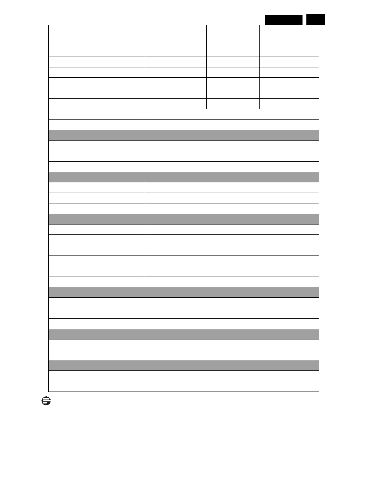
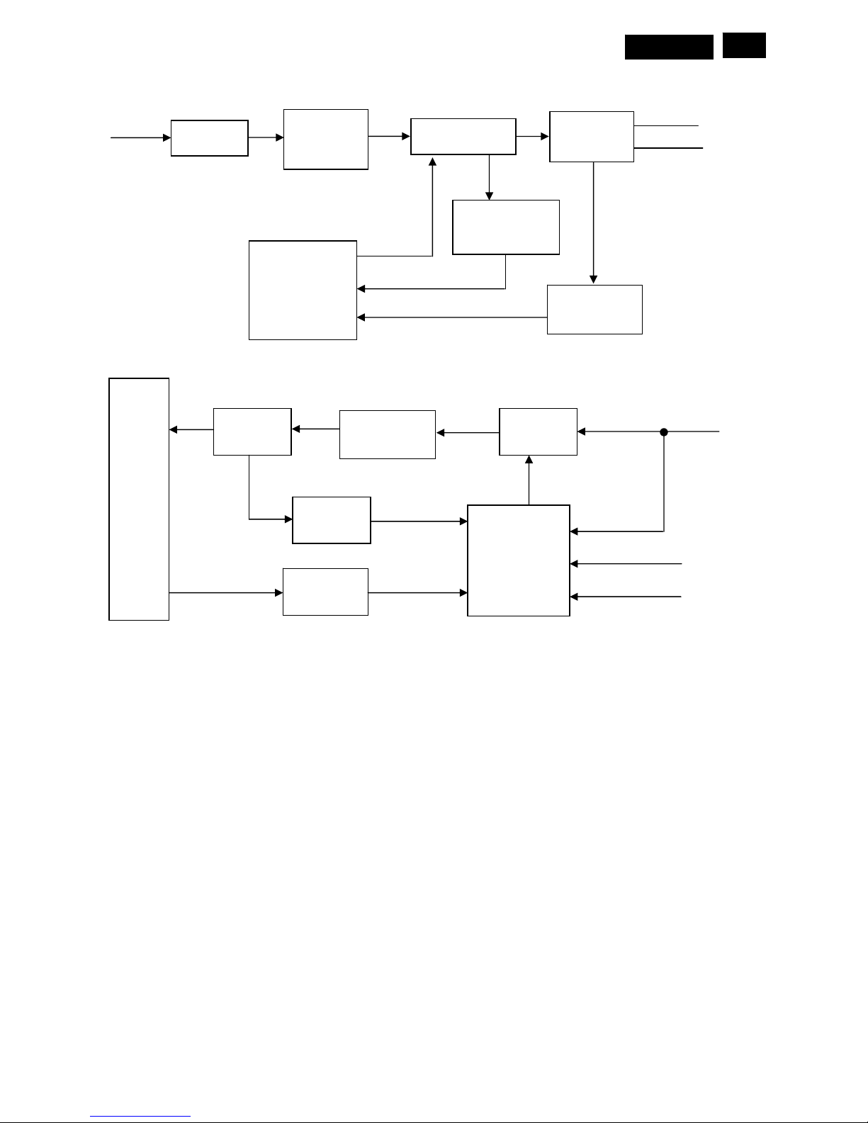
2. LCD Monitor Description
The LCD monitor will contain a scaler board, a power board, a LED board and a key board. The scaler board
houses the flat panel control logic, brightness control logic and DDC.
The power board will provide AC to DC Inverter voltage to drive the backlight of panel and the scaler board chips
each voltage.
Monitor Block Diagram
AC-IN
100V-240V
Power Board
(Include: Adapter, Inverter)
Flat Panel and
CCFL backlight
Scaler Board
DVI-D
D-SUB
CCFL Drive.
Video signal, DDC
Key Board
HOST Computer
LED Board
7
Meridian 2
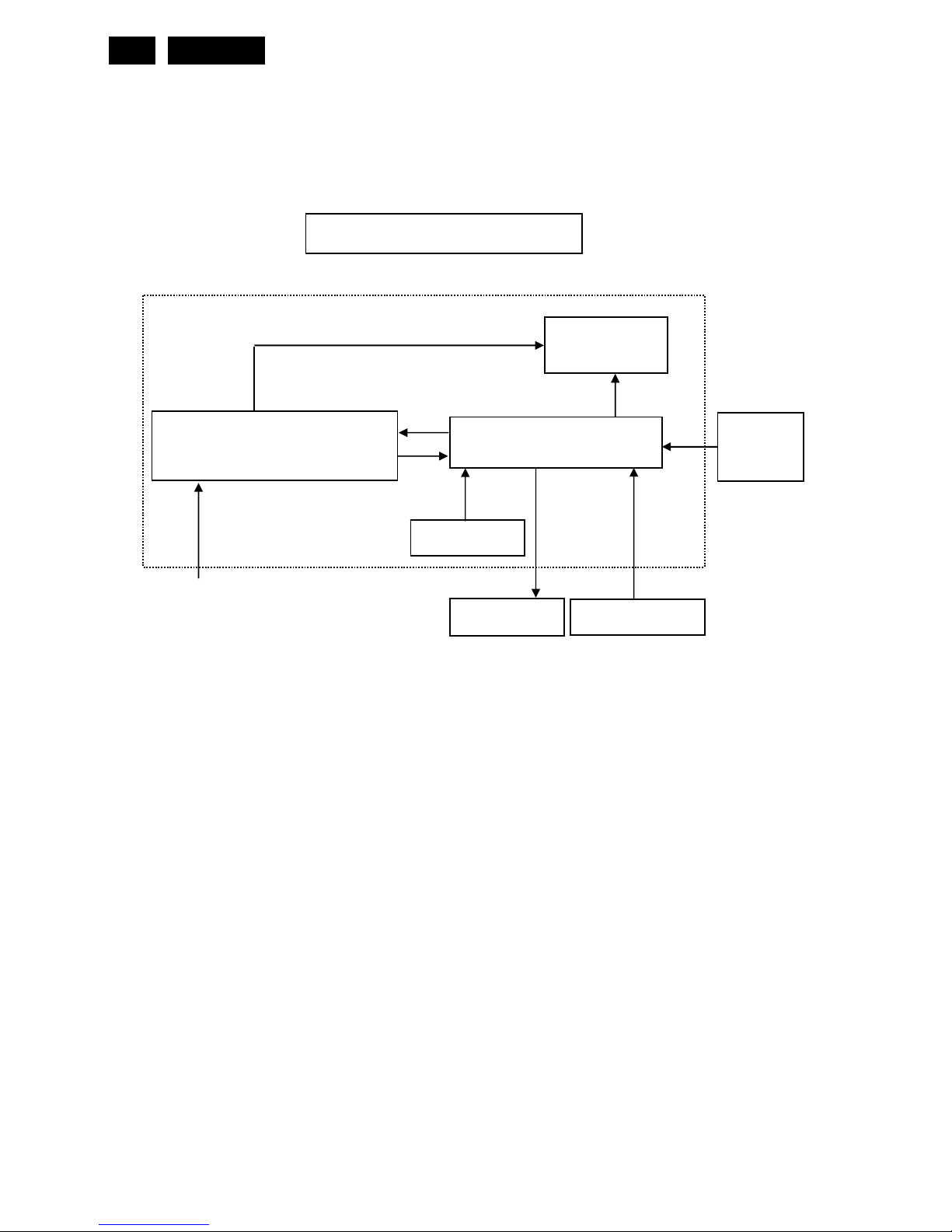
3. Operating Instructions
3.1 General Instructions
Press the power button to turn the monitor on or off.
The other control knobs are located at front panel of
the monitor (see figure). By changing these setting,
the picture can be adjusted to your personal
preference.
﹡The power cord should be connected.
﹡ Press the power button to turn on the monitor.
The power indicator will light up.
3.2 Control Buttons
Operating the Monitor
Connecting to your PC
Connect to PC
1. Connect the power cord to the back of the monitor
firmly.
2. Turn off your computer and unplug its power cable.
3. Connect the monitor signal cable to the video
connector on the back of your computer.
4. Plug the power cord of your computer and your
monitor into a nearby outlet.
5. Turn on your computer and monitor. If the monitor
displays an image, installation is complete.
Install base stand
17. Place the monitor face down a smooth surface
taking care to avoid scratching or damaging the
screen.
Meridian 2
8
2. Hold the monitor base stand with both hands and
firmly insert the base stand into the base column.
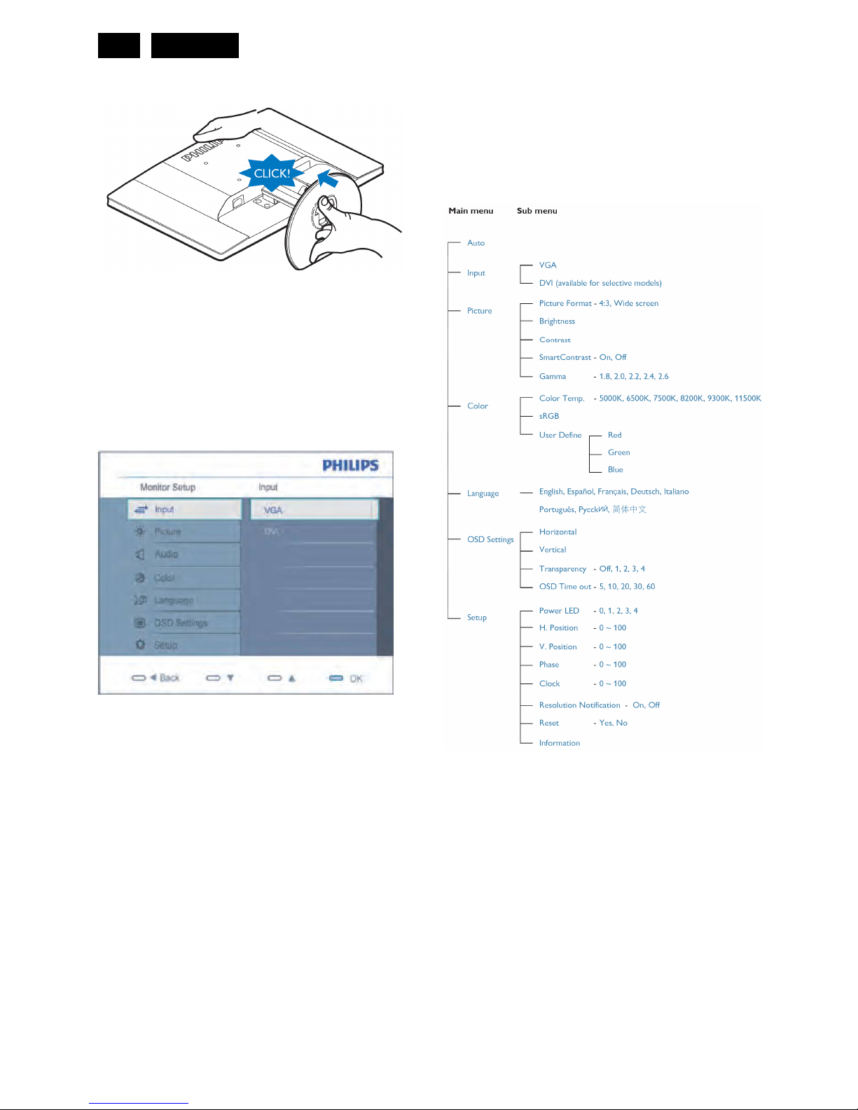
3.3 OSD Menu
On-Screen Display (OSD) is a feature in all Philips
LCD monitors. It allows an end user to adjust screen
performance or select functions of the monitors directly
through an on-screen instruction window. A user
friendly on screen display interface is shown as below:
Basic and simple instruction on the control keys
In the OSD shown above users can press buttons at
the front bezel of the monitor to move the cursor, OK to
confirm the choice or change.
The OSD tree
Below is an overall view of the structure of the
On-Screen Display. You can use this as a reference
when you want to work your way around the different
adjustments later on.

9
Meridian 2
4. Input/ Output Specification
4.1 Input Signal Connector
Analog connectors
Pin No.
Signal Name
Pin No.
Signal Name
1
Red
9
DDC +3.3V or +5V
2
Green/ SOG
10
Logic GND
3
Blue
11
Sense (GND)
4
Sense (GND)
12
Bi-directional data
5
Cable Detect (GND)
13
H/H+V sync
6
Red GND
14
V-sync
7
Green GND
15
Data clock
8
Blue GND
Digital connectors (Option)
Pin No.
Signal Name
Pin No.
Signal Name
1
T.M.D.S. data2-
13
No Connect
2
T.M.D.S. data2+
14
+5V Power
3
T.M.D.S. data2 shield
15
Ground (for +5V)
4
No Connect
16
Hot plug detect
5
No Connect
17
T.M.D.S. data0-
6
DDC clock
18
T.M.D.S. data0+
7
DDC data
19
T.M.D.S. data0 shield
8
No Connect
20
No Connect
9
T.M.D.S. data1-
21
No Connect
10
T.M.D.S. data1+
22
T.M.D.S clock shield
11
T.M.D.S. data1 shield
23
T.M.D.S. clock+
12
No Connect
24
T.M.D.S. clock-

Meridian 2
10
4.2 Resolution & Preset Modes
Maximum Resolution
1680 x 1050 at 60 Hz (analog input)
1680 x 1050 at 60 Hz (digital input)
Recommended Resolution
1680 x 1050 at 60 Hz (digital input)
Resolution H. freq (kHz) V. freq (Hz)
640x350 31.469 70.086
720x400 31.469 70.086
640x480 31.469 59.940
640x480 35.000 67.000
640x480 37.500 75.000
800x600 35.156 56.250
800x600 37.879 60.317
800x600 46.875 75.000
1024x768 48.363 60.004
1024x768 60.023 75.029
1280x1024 63.981 60.020
1280x1024 79.976 75.025
1440x900 55.469 59.901
1440x900 55.935 59.887
1440x900 70.635 74.984
1920x1080 66.587 60.000 (reduce blinking)
1680x1050 65.290 60.000
1680x1050 64.674 60.000
11
Meridian 2
4.3 Pixel Defect Policy
Philips strives to deliver the highest quality products.
We use some of the industry’s most advanced
manufacturing process and practice stringent quality
control. However, pixel or sub pixel defects on the TFT
LCD panels used in flat panel monitors are sometimes
unavoidable. No manufacturer can guarantee that
panels will be free from pixel defects, but Philips
guarantees that any monitor with an unacceptable
number of defects will be repaired or replaced under
warranty. This notice explains the different types of
pixel defects and defines acceptable defect levels for
each type. In order to qualify for repair or replacement
under warranty, the number of pixel defects on a TFT
LCD panel must exceed these acceptable levels. For
example, no more than 0.0004% of the sub pixels on a
19″ XGA monitor may be defective. Furthermore,
Philips sets even higher quality standard for certain
types or combinations of pixel defects that are more
noticeable than others. This policy is valid worldwide.
Pixels and Sub pixels
A pixel, or picture element, is composed of three sub
pixels in the primary colors of red, green and blue.
Many pixels together form an image. When all sub
pixels of pixel are lit, the three colored sub pixels
together appear as a single white pixel. When all are
dark, the three colored sub pixels together appear as a
signal black pixel. Other combinations of lit and dark
sub appear as single pixels of other colors.
Types of Pixel Defects
Pixel and sub pixel defects appear on the screen in
different ways. There are two categories of pixel
defects and several types of sub pixel defects within
each category.
Bright Dot Defects Bright dot defects appear as pixels
or sub pixels that are always lit or ‘on’. That is, a Bright
dot is a sub-pixel that stands out on the screen when
the monitor displays a dark pattern. There are three
types of bright dot defects:
One lit red, green or blue sub pixel
Two adjacent lit sub pixels:
- Red + Blue = Purple
- Red + Green = Yellow
- Green + Blue = Cyan (Light Blue)
Three adjacent lit sub pixels (one white pixel)
Note:
A red or blue bright dot must be more than
50 percent brighter than neighboring dots while a
green bright dot is 30 percent brighter than
Meridian 2
12
neighboring dots.
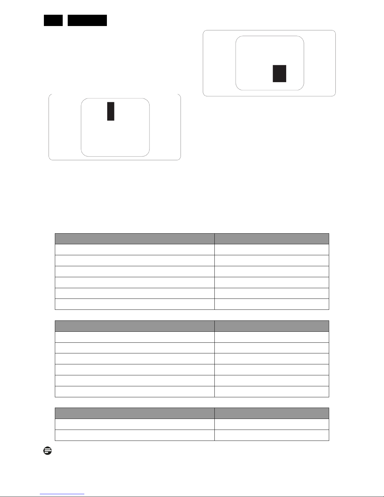
Black Dot Defects Black dot defects appear as pixels
or sub pixels that are always dark or ‘off’. That is, a
dark dot is a sub-pixel that stands out on the screen
when the monitor displays a light pattern. There are
two types of black dot defects:
Proximity of Pixel Defects
Because pixel and sub pixels defects of the same type
that are near to one another may be more noticeable,
Philips also specifies tolerances for the proximity of
pixel defects.
Pixel Defect Tolerances
In order to qualify for repair or replacement due to pixel
defects during the warranty period, a TFT LCD panel in
a Philips flat panel monitor must have pixel or sub pixel
defects exceeding the tolerances listed in the following
tables.
Bright Dot Defects Acceptable level
MODEL 220S2
1 lit subpixel 3
2 adjacent lit subpixels 1
3 adjacent lit subpixels (one white pixel) 0
Distance between two bright dot defects* >15mm
Total bright dot defects of all types 3
Black Dot Defects Acceptable level
MODEL 220S2
1 dark subpixel 5 or fewer
2 adjacent dark subpixels 2 or fewer
3 adjacent dark subpixels 0
Distance between two black dot defects* >15mm
Total black dot defects of all types 5 or fewer
Total Dot Defects Acceptable level
MODEL 220S2
Total bright or black dot defects of all types 5 or fewer
Note:
1 or 2 adjacent sub pixel defects = 1 dot defect
This monitor is ISO9241-307 compliant
13
Meridian 2
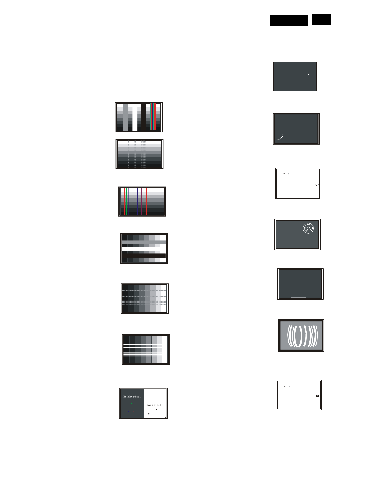
4.4 Failure Mode Of Panel
Failure description
Phenomenon
Vertical block defect
Vertical dim lines
Vertical lines defect
(Always bri
g
ht or dark)
Horizontal block defect
Horizontal dim lines
Horizontal lines defect
(Always bri
g
ht or dark)
Has bri
g
ht or dark pixel
Polarizer has bubbles
Polarizer has bubbles
Foreign material inside
polarizer. It shows liner or
dot shape.
Concentric circle formed
Bottom back light of LCD is
brighter than normal
Back light un-uniformity
Backli
g
ht has foreign material.
Black or white color, liner or
circular type
Quick reference for failure mode of LCD panel
this pa
g
e presents problems that could be made by LCD panel.
It is not necessary to repair circuit board. Simply follow the mechanical
instruction on this manual to eliminat e failure by replace LC D pan el.

Meridian 2
14
5. Block Diagram
5.1 Scaler Board
Flash Memory
PM25LV020-100SCE
(U402)
Panel Interface
(CN301)
Crystal
12MHz
(
X401)
Keypad Interface
(CN402)
D-Sub Connector
(CN101)
EDID_WP
DDCSCL1
DDCSDA1
DVI Connector
(CN102)
EEPROM
AT24C02BN
(
U101)
EEPROM
AT24C02BN
(U102)
EDID_WP
DDCSCL2
DDCSDA2
Scaler IC NT68668FG
(Include MCU, ADC, OSD)
(U401)
RX+/-
RXC+/-
RGB
H/Y Sync
15
Meridian 2
5.2 Power Board
EMI filter
PWM Control
TOP266
(IC901)
Transformer
AC input
16V
5V
Bridge
Rectifier
and Filter
Feedback
Circuit
Rectifier
Diodes
Photocoupler
(IC903)
ON/OFF
Feedback
Circui
t
Transformer
(PT801)
Lamp
Output
Circui
t
PWM Control
Ta9687
(IC801)
16V
DIM
MOSFET
A
O4614
16V
Protect
Circui
t
16
Meridian 2
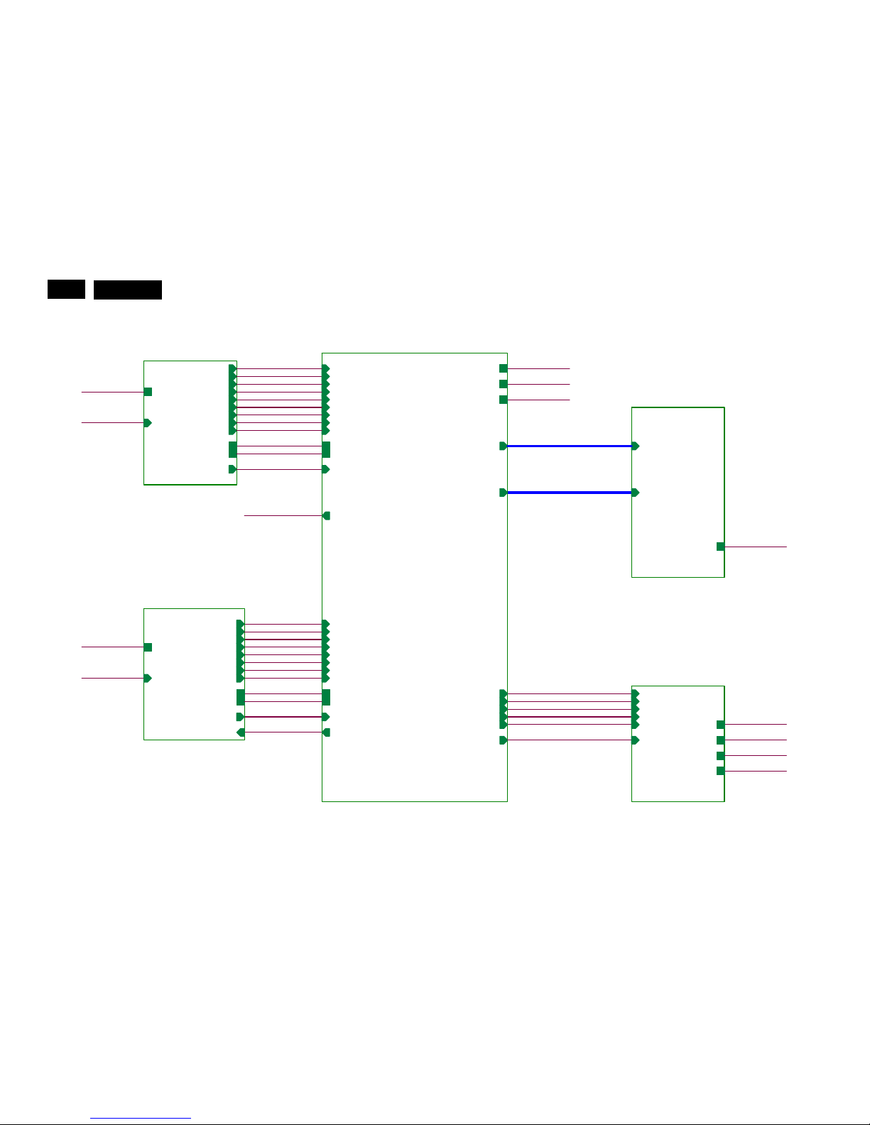
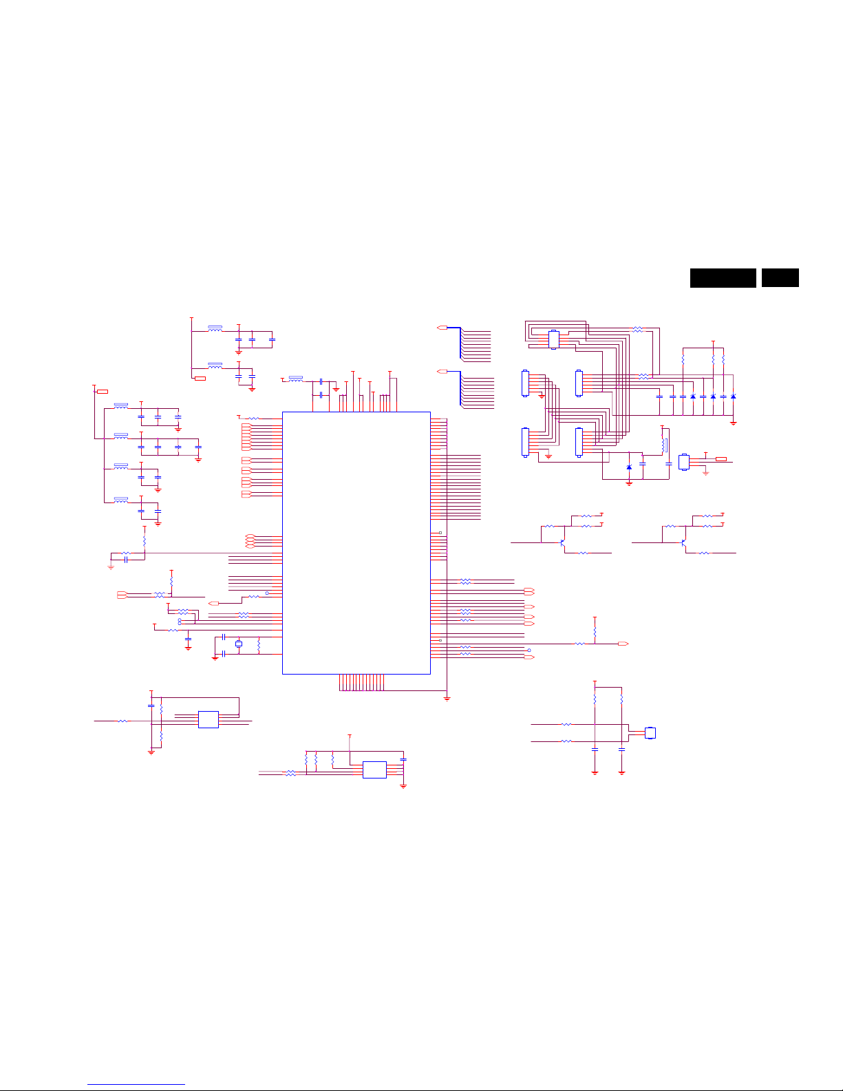
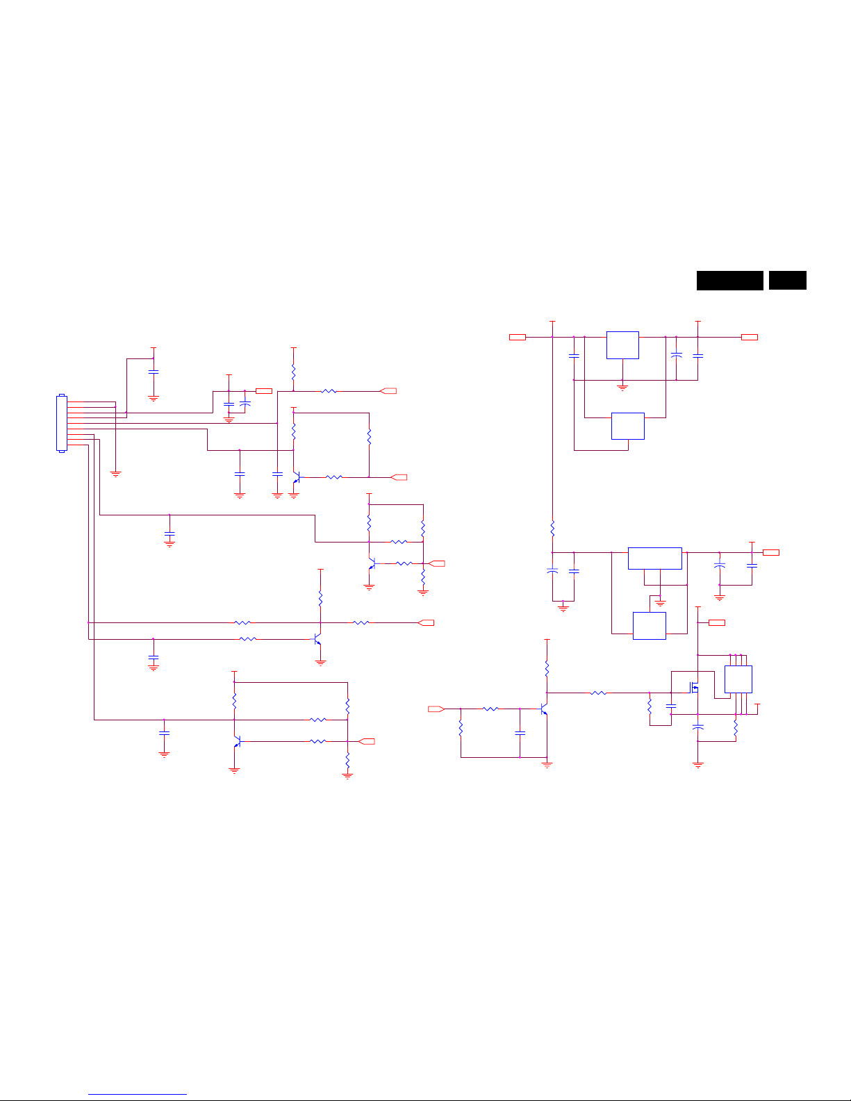
6. Schematic
6.1 Scaler Board (715G3737M0D0000H4K)
VLCD
RX0-
+5V
PA[0.. 9]
PB[0.. 9]
SOG_DET
Adj_BACKLIGH T
RX1+
02.IN PUT
02.D-SUB INPUT
R0+
R0-
SOG_DET
G0+
G0-
B0+
B0-
+5V
AHS0
AVS0
DDCSCL1
DDCSDA1
EDID _WP
VGA_CABLE_DET
DDCSCL2
G0-
05.PANEL I NTERF ACE
05.PANEL I NTERF ACE
VLCD
PA[0.. 9]
PB[0.. 9]
AHS0
on_BACKLIGH T
+5V
Audio_EN
B0+
RXC-
DDCSDA1
VCC1.8
DDCSCL1
DVI_CABLE_DET
04.SCALER
04.SCALER
Adj_BACKLIGH T
on_BACKLIGH T
Audio_EN
Audio_DET
PS_EN
Panel_ON
PB[0.. 9]
PA[0.. 9]
R0+
R0SOG_DET
G0+
G0B0+
B0AHS0
AVS0
DDCSCL1
DDCSDA1
EDID _WP
VGA_CABLE_DET
RXC+
RXC-
RX2-
RX2+
RX1+
RX1-
RX0-
RX0+
DDCSCL2
DDCSDA2
DVI_C ABLE_DET
DVI_HPD
VCC1. 8
VCC3. 3
+5V
R0-
RX0+
EDID _WP
Audio_DET
PS_EN
DVI_HPD
VGA_CABLE_DET
RX1-
EDID _WP
+5V
VLCD
VCC3. 3
VCC1.8
RXC+
VCC3. 3
03.DVI INPUT
03.DVI INPUT
RX0+
RX0-
RX1-
RX1+
RX2+
RX2-
RXC-
RXC+
DDCSCL2
DDCSDA2
DVI_C ABLE_DET
EDID _WP
+5V
DVI_HPD
RX2-
RX2+
+5V
R0+
G0+
06.POWER
06.POWER
Adj_BACKLIGH T
on_BACKLIGH T
Audio_EN
Audio_DET
PS_EN
Panel_ON
+5V
VCC3. 3
VCC1. 8
VLCD
B0-
DDCSDA2
EDID _WP
Panel_ON
AVS0
17
Meridian 2
Remark: Parts position can be searched by using FIND function in PDF.
C114
0.1uF 25V
R142
470R 1/16W 5%
C111
NC/ 22pF 50V
B0+
RIN0
R106
100R 1/16W 5%
+5V4,5,7
B0+ 5
R117
0R05 1/16W
R0+
DDCSDA15
R126
2K2 1/16W 5%
R107
75R 1/16W 1%
VSIN0
U102
AOZ8902CIL
1
2
3 4
5
6
CH1
VN
CH2CH3
VP
CH4
DDCSDA_A
R112
75R 1/16W 1%
C110
47nF 16V
R108
100R 1/16W 5%
RIN0-
R105
100R 1/16W 5%
DDCSCL_A
BIN0
GIN0
HSIN0
BIN0-
RIN0
DDCSCL_A
C103
5PF 50V
R123 100R 1/16W 5%
R111
100R 1/16W 5%
U103
AOZ8902CIL
1
2
3 4
5
6
CH1
VN
CH2CH3
VP
CH4
R119
100R 1/16W 5%
AHS0 5
B0- 5
DDCSCL1
R102 100R 1/16W 5%
B0-
R109
0R05 1/16W
R0- 5
GIN0-
DDCSCL15
RIN0
R118
0R05 1/16W
R125
2K2 1/16W 5%
C102
47nF 16V
ZD101
RLZ5.6B
R0-
HSIN0
GIN0
R120
75R 1/16W 1%
D-SUB
C101
220nF 16V
C181
22pF 50V
R0+ 5
C113
0.1uF 25V
VSIN0
DDCSCL1
D101
BAV70
3
1
2
ESD_VGA
U101
AT24C02BN-SH-T
1
2
3
45
6
7
8
A0
A1
A2
VSSSD A
SCL
WP
VCC
VSIN0
C182
22pF 50V
C109
5PF 50V
G0- 5
G0-
R121
100R 1/16W 5%
C106
5PF 50V
SOG_DET 5
DET_VGA
DDCSDA1
G0+ 5
G0+
R115 4K7 1/16W 5%
DET_VGA
+5V
DDCSDA1
ESD_VGA
R104
0R05 1/16W
BIN0-
BIN0
DDCSDA_A
C107
47nF 16V
C105 47nF 16V
VGA_CABLE_DET 5
C120
1000pF 50V
R101
100R 1/16W 5%
C112
NC/ 22pF 50V
R122 0R05 1/10W
R113
100R 1/16W 5%
ESD_VGA
C108
47nF 16V
VGA_5V
EDID _WP
GIN0-
BIN0
R114 4K7 1/16W 5%
VGA_5V
C104
47nF 16V
VGA_5V
R116 22K 1/16W 5%
EDID_W P4,5
GIN0
RIN0-
R124 100R 1/16W 5%
R103
0R05 1/16W
VGA_CABLE_DET
R110
0R05 1/16W
CN101
DB15
1
6
2
7
3
8
4
9
5
11
12
13
14
15
10
17 16
AVS0 5
HSIN0
18
Meridian 2
Remark: Parts position can be searched by using FIND function in PDF.
HPD
R138 10R 1/16W 5%
RX2- 5
DDC_WP
R128 100R 1/16W 5%
EDID_WP 3,5
DAT1-
+5V3,5,7
DVI_HPD 5
DCLK-
DVI5V
U107
AOZ8902CIL
1
2
3 4
5
6
CH1
VN
CH2C H3
VP
CH4
DAT0-
DVI5V
R140 10R 1/16W 5%
ZD102
RLZ5.6B
DCLK+
R127
100R 1/16W 5%
R133 22K 1/16W 5%
U106
AOZ8902CIL
1
2
3 4
5
6
CH1
VN
CH2CH3
VP
CH4
C116
220nF 16V
D102
BAV70
3
1
2
RX0- 5
DVI5V
R130 1K 1/ 16W
ESD_DVI
C117
0.1uF 25V
RX1- 5
ESD_DVI
Q101
NC
U105
AT24C02BN-SH -T
1
2
3
45
6
7
8
A0
A1
A2
VSSSDA
SCL
WP
VCC
DVI
CN102
JACK
1
2
3
4
5
6
7
8
9
10
11
12
13
14
15
16
17
18
19
20
21
22
23
24
262527
28
DAT2-
DAT2+
2/4shield
DAT4-
DAT4+
DDC SCL
DDC SDA
VSYNC
DAT1-
DAT1+
1/3shield
DAT3-
DAT3+
+5V
SYNC GND
HPD
DAT0-
DAT0+
0/5shield
DAT5-
DAT5+
clk shield
clk+
clk-
GND
GND
GND
GND
U104
AOZ8902CIL
1
2
3 4
5
6
CH1
VN
CH2C H3
VP
CH4
RX0+ 5
ESD_DVI
DAT0+
C119
0.1uF 25V
ESD_DVI
RX1+ 5
RXC+ 5
DAT1+
DAT2- R139 10R 1/16W 5%
DAT2+
DET_DVI
C115
0.1uF 25V
R137 10R 1/16W 5%
R134 10R 1/16W 5%
ESD_DVI
SCL_DVI
R132 4K7 1/16W 5%
R141 10R 1/16W 5%
R135 10R 1/16W 5%
R136 10R 1/16W 5%
RX2+ 5 DDCSCL2 5
DDCSDA2 5
+5V
ESD_DVI
R129 100R 1/16W 5%SDA_DVI
R131 4K7 1/16W 5%
RXC- 5
DVI_CA BLE_DET 5
C118
0.1uF 25V
19
Meridian 2
Remark: Parts position can be searched by using FIND function in PDF.
+5V
VCC3.3
DVDD
KEY2
PA5
C421
4.7UF 10V
C0805
AVCC
PB7
C422
0.1uF 25V
PB[0..9]6
+5V 3,4,7
RXC-4
VCC3.3
VCC3.3
USB_EN
CN405
NC/CONN
1
2
3
4
5
6
7
C428 22P 50V
LVB0PFB407
NC/300OHM
DDCSDA13
TP4
R405
NC/3K9 +/-5% 1/16W
KEY2
LVA3P
FB406
300OHM
1 2
R444
10K 1/16W 5%
R441 NC/4.7K 1/16W
LVB1M
BUZZER
R424 330R 1/16W 5%
C417
0.1uF 25V
ADC_VAA
RX1-
LVACKP
AHS0
EE_WP
D402
RLZ5.6B
G0-3
DVDD
+5V
VCC3.3
CN406
NC/CONN
1
2
3
R416
220K 1/16W 5%
C423
4.7UF 10V
C0805
POWER
LVA2M
R446 NC/0R05 1/16W
PA9
PA6
PA1
R414 0R05 1/16W
R420 120R 1/16W 1%
C401
0.1uF 25V
FB403
300OHM
RX0+4
KEY1
SPI_SI
LVA0M
G0-
R0+
R426 NC/100R 1/16W 5%
ADC_BIAS
PB0
LED_1
CN404
CONN
1
2
3
4
5
6
7
R443 NC/4.7K 1/16W
ADC_BIAS
VCC3.3
PB4
VCC3.3
RX0+
LVA0P
LVACKM
PA4
LVB2M
LVB0M
R434 NC/100R 1/16W 5%
R428 NC/100R 1/16W 5%
VCC1.8 7
RX0-
LVB2P
PA6
CN401
NC/CONN
2
4
6
8
1
3
5
7
C413
4.7UF 10V
C0805
LED_A
C426 22P 50V
TP1
PB4
R429
10K 1/16W 5%
R445
NC/100R 1/16W 5%
LVB3M
LVBCKP
C412
NC/0.1uF 25V
PA[0..9]6
Panel_ON 7
VCC3.3
Audio_EN 7
LVA1M
SOG_DET3
VCC3.3
R425 10K 1/16W 5%
R415
100K 1/16W 5%
DDCSDA24
AVCC
LVA0M
PB9
DDCSDA2
R435 NC/10K 1/16W 5%
MSDA
C430
NC/220N16V
C408
0.1uF 25V
R438
NC/10K 1/16W 5%
LED_1
R407 330R 1/16W 5%
Q401
2N3906S-RTK/PS
C414
1uF 10V
C0402
RXC+
LVB3M
PA3
R436
NC/22K 1/16W 5%
Audio_DET 7
D403
RLZ5.6B
ADC_VAA
WP
LED_2
R411
2K2 1/16W 5%
SPI_SO
EE_WP
C405
0.1uF 25V
ADC_VAA33
MSCL
C424
1uF 10V
C0402
VCC3.3
PA[0..9]
Adj_BACKLIGHT
EDID_WP
Scaler
ADC_VAA33
PA7
USB_DET
R410 NC
R401
NC/3K9 +/-5% 1/16W
LVA0P
LVACKP
R418
820R 1/10W 5%
PS_EN 7
Audio_DET
PB8
AHS03
VSO
HSO
PA2
PA5
Audio_EN
CABLE_DET
U401
NT68668FG
1
2
3
4
5
6
7
8
9
10
11
12
13
14
151617
18
19
20
21
22
23
24
25
262728
29
30
31
32
33
34
35
36
37
38
39
40
41
42
434445
46
47
48
49
50
515253
54
55
56
57
58
59
60
61
62
63
64
102
101
100
99
98
97
96
95
94
93
92
91
90
89
88
87
86
85
84
83
82
81
80
79
78
77
76
75
74
73
72
71
70
69
68
67
66
65
128
127
126
125
124
123
122
121
120
119
118
117
116
115
114
113
112
111
110
109
108
107
106
105
104
103
RSTB
DVDD_ZP
DGND
RX2+
RX2-
AVCC
RX1+
RX1-
AGND
RX0+
RX0-
AGND
RXC+
RXC-
AVCC
REXT
ADC_BIAS
PGND
BIN1+
BIN1-
SOG1I
GIN1+
GIN1-
RIN1+
RIN1-
ADC_VAA18
ADC_GNDA
ADC_VAA33
PD6
PB3/ADC3/INTE1
P31/TXD
P30/RXD
PB2/ADC2/INTE0
PB7/DDC_SDA1*
PB6/DDC_SCL1*
PA3/PWM5
PA4/PWM6*
PA5/PWM7*
PA6/PWM8*
PA7/PWM9*
HSYNCI1
VSYNCI1
PLL_GND
GND
PLL_DVDD
PB5/DDC_SDA0*
PB4/DDC_SCL0*
PD5
P35
P34
DVDD
CVDD
NC
V0
V1
V2
V3
V4
V5
V6
V7
VCKI
DGND/CGND
DGND/CGND
PC6
DGND/CGND
DGND/CGND
DGND/CGND
DGND/CGND
DGND/CGND
DGND/CGND
DGND/CGND
DGND/CGND
DGND/CGND
DGND/CGND
DGND/CGND
DVDD
DGND/CGND
T0M
T0P
T1M
T1P
T2M
T2P
TCLK1M
TCLK1P
T3M
T3P
DGND/CGND
T4M
T4P
T5M
T5P
T6M
T6P
TCLK2M
TCLK2P
T7M
T7P
PA1/PWM3
PA2/PWM4
PA0/PWM2
OSCO
OSCI
PB0/ADC0
PB1/ADC1
PC5
PC4/PWM1
PC3/PWM0
PC1*
PC0*
CVDD_ZP
PWMB*
PWMA*
DVDD
CVDD
INT_HSO
INT_VSO
DGND
DGND
PC2
GND
PD4
SPI_CLK
SPI_SI
SPI_SO
SPI_CE
PC7
R413
NC/2K2 1/16W 5%
B0-3
DVDD
RXC-
VGA_CABLE_DET
R412 NC/0R05 1/16W
AVS03
VCC3.3
PB6
LVB1P
R431
100R 1/16W 5%
VCC3.3 7
PA8
DVI_HPD 4
DVDD
KEY1
PB5
USB_EN
C404
4.7UF 10V
C0805
LVB1P
C429
220nF 16V
FB401
300OHM
LVBCKM
LVBCKM
LED_2
R423 220K 1/16W 5%
C418
0.1uF 25V
R0+3
DDCSCL24
DVI_CABLE_DET
C403
0.1uF 25V
LED_G
PB7
R406 330R 1/16W 5%
R440 NC/0R05 1/16W
SPI_CK
C415
1uF 10V
C0402
RX1-4
PB1
PA4
LVB1M
LVB3P
X401
12MHz
1 2
LVA1P
PB5
R408
470R 1/16W 1%
RX2+
LVA2P
PA2
R404
NC/3K9 +/-5% 1/16W
R419
390K +/-5% 1/16W
CN403
NC/CONN
1
2
3
4
5
6
5V_DET
PB6
R439 100R 1/16W 5%
C431
NC/0.1uF 25V
Q402
2N3906S-RTK/PS
C406
1uF 10V
LVA3M
AVS0
RX2-
C427
0.1uF 25V
HSO
TP3
D404
NC/RLZ5.6B
PB2
SPI_SO
R433
NC/10K 1/16W 5%
TP5
SPI_CK
PB9
DDCSCL2
C409
0.1uF 25V
FB408
300OHM
C411
NC/0.1uF 25V
R409 0R05 1/16W
G0+3
CVDD
SPI_CE
U403
NC/M24C16
1
2
3
45
6
7
8
A0
A1
A2
GNDSDA
SCL
WP
VCC
B0+
FB404
300OHM
SOG_DET
DDCSDA1
CN407
NC/CONN
1
2
on_BACKLIGHT 7
PB3
R442 NC/4.7K 1/16W
PB8
C425 0.1uF 25V
FB405
300OHM
WP
PB0
DDCSCL1
PB2
SPI_SI
R417
100R 1/10W 5%
R452 NC
RX2+4
LED_A
USB_DET
DVI_HPD
C432
NC/0.1uF 25V
DDCSCL13
LVB0M
R447
NC/100R 1/16W 5%
Adj_BACKLIGHT 7
PB[0..9]
R421 100R 1/16W 5%
R0-3
PA9
Panel_ON
AVCC
LVBCKP
PA0
RX1+4
+5V
+5V
LVA1P
C416
4.7UF 10V
C0805
+5V
R427 100K 1/16W 5%
CVDD
R430
NC/22K 1/16W 5%
R422 100K 1/16W 5%
EDID_WP
R451 NC
FB402
300OHM
B0+3
RX1+
C419
0.1uF 25V
R403 NC/2K2 1/16W 5%
RX0-4
VCC1.8
LVA1M
G0+
C437
1UF 10V
C420
1UF 10V
PA7
R437
NC/22K 1/16W 5%
C402
0.1uF 25V
PB1
LVB2P
BUZZER
POWER
MSDA
C410
1N 50V
LVB0P
LVACKM
PA1
DVI_CABLE_DET4
MSCL
LVB2M
LVA3P
D401
NC/RLZ5.6B
R402 NC/2K2 1/16W 5%
VSO
R0-
PS_EN
R432
1M 1/16W
PA3
PA0
U402
PM25LV020-100SCE
1
2
3
4
8
7
6
5
CE#
SO
WP#
GND
VDD
HOLD#
SCK
SI
RXC+4
LVA3M
CABLE_DET
C407
0.1uF 25V
PA8
TOUCH_POWER
VGA_CABLE_DET3
LVA2P
B0-
on_BACKLIGHT
RX2-4
LVA2M
LED_G
CN402
NC/CONN
1
2
3
4
5
6
PB3
SPI_CE
LVB3P

20
Meridian 2
Remark: Parts position can be searched by using FIND function in PDF.
RXE3-
Panel Interface
RXO0+
LVB3M
RXE0+
LVACKP
LVB0M
LVBCKM
RXO3-
RXO3+
LVA2M
RXO0+
LVB2P
LVA3P
PB2
R448220 OHM 1/ 4W
RXOC-
RXEC-
+
C433
100uF16V
PA9
RXE1-
RXEC+
RXOC+
RXO2+
PA3
LVACKM
RXO1+
RXE3-
PB7
PB9
LVA1M
LVB2M
LVB3P
RXEC+
LVB1M
RXO2-
LVB3M
LVA0P
LVB1MLVA1P
C435
NC
RXOC-
LVA3P
PB5
PB[0.. 9]
RXEC-
LVB2M
PB[0.. 9]5
RXO2+
C434
0.1uF 25V
LVB3P
RXO3+
LVBCKP
RXO1-
LVACKM
LVA2P
RXE2-
PB3
RXEC-
LVACKP
RXE0-
RXO1+
RXO0-
LVA2P
RXO2-
LVB0P
VLCD
RXOC+
LVBCKM
RXO1-
PB0
PA0
PA[0.. 9]5
LVBCKP
CN409
NC/CONN
2
4
6
8
10
12
14
16
18
20
22
24
26
28
30
1
3
5
7
9
11
13
15
17
19
21
23
25
27
29
PB8
LVB2P
RXO3-
LVA1P
LVA2M
R449220 OHM 1/ 4W
LVA0M
VLCD 7
RXEC+
RXE3+
LVB1P
LVA3M
PA7
LVA3M
RXE0+
RXE2-
RXE2+
RXE1-
PB6
LVB1P
RXE2+
PA4
LVB0M
PB4
RXOC-
RXE0-
PB1
RXOC+
PA6
CN408
CONN
1
2
3
4
5
6
7
8
9
10
11
12
13
14
15
16
17
18
19
20
21
22
23
24
25
26
27
28
29
30
PA5
RXE3+
LVA1M
PA2
LVA0M
FB409
120 OHM
1 2
PA8
LVB0P
PA1
PA[0.. 9]
RXO0-
LVA0P
RXE1+
RXE1+
C436
NC
21
Meridian 2
Remark: Parts position can be searched by using FIND function in PDF.
U701
3 2
1
VIN VOUT
GND
Audio_DET 5
Q707
NC/PMBS3904
VCC1. 8 5
C715
220nF 16V
ON/OFF
C714
NC/0.1uF 25V
VLCD 6
+5V 3, 4,5
R715
56KOHM 1/16W
VCC3. 3 5
Audio_DET1
Q704
NC/ AO4449 -7A/-30V
123
4
876
5
SSS
G
DDD
D
+5V3, 4,5
C712
0.1uF 25V
+
C710
100UF16V
U702
NC/G1084-33T43Uf
23
1
VOUTVIN
GND
R706
NC/1 0K 1/16W 5%
+
C711
NC/10 0uF/16V
+5V
R707
4.7 OHM +-5% 2WS
VCC3. 3
C708
NC
TO252
R716
NC/1 0K 1/16W 5%
R721
10K 1/16W 5%
VCC3. 3
R724
NC
R718
NC
C707
0.1uF 25V
VCC1.8
R799
10K 1/16W 5%
Q705
AO3401A
U704
3 2
1
VIN VOUT
GND
C706
0.1uF 25V
VCC3. 3
+5V
R703 1K 1/16 W
Audio_DET2
R702
10K 1/16W 5%
C704
0.1uF 25V
C709
NC/0.1uF 25V
+5V
Power
R717
NC
R701
22K 1/16W 5%
R714
10K 1/16W 5%
C701
0.1uF 25V
R723
NC/4K7 1/16W 5%
C713
0.1uF 25V
Adj_BACKLIGH T 5
VCC3. 3
R704
10K 1/16W 5%
Q703
NC/PMBS3904
R713
NC
+
C705
100uF16V
R709
NC/22K 1/16W 5%
R711 NC /100R 1/16W 5%
PS_EN 5
U703
AME8815BEGT180Z
1234
GND
VOUT(heat sink )VIN
4
Q702
NC/2N3904S-RTK/PS
Audio_EN 5
R710
NC/1 00K 1/16W 5%
R708
NC/0 R05 1/16W
Audio_EN1
VLCD
R725
NC
+
C716
10UF16V
CN701
CONN
1
2
3
4
5
6
7
8
9
R712 NC /100R 1/16W 5%
on_BACKLIGH T 5
R719
22K 1/16W 5%
Q701
2N3904S-RTK/PS
+5V
R720
NC
VCC3.3
C718
220nF 16V
Panel_ON5
+
C702
100uF16V
C717
NC/0.1uF 25V
TO-252
C703
0.1uF 25V
R798
NC
Q706
2N3904S-RTK/PS
R722
NC/ 10K 1/16W 5%
+5V
+5V
DIM
22
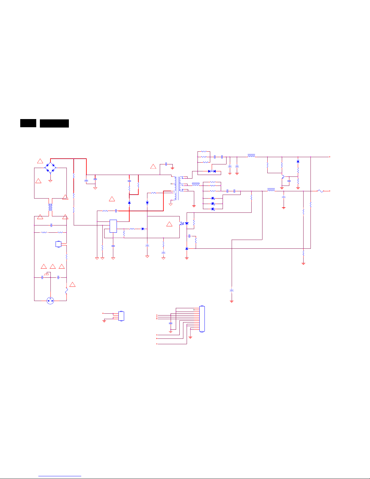
Meridian 2
6.2 Power Board (715G3974P01000001S)
Remark: Parts position can be searched by using FIND function in PDF.
R939
1K 1/8W
R943
470OHM +-5% 1/8W
R930
9.53K 1/10W 1%
R902
1M
MUTE
R935 100 OH M 1/4W
+
C905
100uF M 450V
067G 40Z10115L
+16V
T901
1.295mH
1
2
3
6
7
8
9
10
11
12
5
+
C918
680uF25V
VOL
F903
FUSE
IC901
TOP266EN
1
2
3
4
5 7
V
X
C
F
SD
C935
1000P 500V
R924
470R 1/8W 5%
+
C915
470uF 16V
C912
1000P 500V
C910
1000P 500V
!
+
C908
22uF 50V
D905 NC
1 2
L903
Coil
!
R903
6R8 +-5% 1/8W
CN902
CONN
1
2
3
4
5
6
7
8
9
10
11
12
13
CN901
SOCKET
12
3
C900
3300PF/250V
-
+
BD901
D2SB80
2
1
3
4
!
R910
10K 1/4W
NC
C907
1500PF2KV
IC904
KIA431A-AT/P
ZD901
MTZJ T-72 22B DO-34
C931
100N 50V
R918
100 OHM 1/4W
R962 100 OH M 1/4W
ON/OFF
C903
0.22UF275V
+
C916
1000uF 10V
R940
NC
!
ZD902
HZ24-2-E
R908
8.87K 1/8W
Q903
KTD1028
C906
0.01uF/2KV
R919
100 OHM 1/4W
R927
10K 1/10W 1%
R920
100 OHM 1/4W
FB901
BEAD
1 2
!
R926
1K 1/10W 1%
C923
100N 50V
NR901
NTCR
DIM
+
C909
47uF 50V
F901
FUSE
C929
1000P 500V
!
!
+
C917
680uF25V
R906
10R 1/8W 5%
R946
470OHM2W
R947
470OHM2W
+16V
+5V1
IC903
PC123X2YFZOF
12
43
!
R911
91KOHM +-1% 1/8W
预留跳线
+5V
D903 SR 504-30
1 2
!
C901
1000pF
R925
NC
R913
NC
R904
100K OMH 2W +-5%
+5V
R961 100 OH M 1/4W
CN905
NC
1
2
D902
FR103
93G 6038T52T
!
R909
NC
L901
30mH
1
4
2
3
R912
0 OHM 1/4W
C922
NC
D904 SR 504-30
1 2
D906
MBRF10150CT
123
!
C932
1N 50V
R901
1M
L904
Coil
CN903
NC/CONN
1
2
3
4
D901
FR107
C924
100N 50V
R907
NC
C902
1000pF
!
R905
NC
23
Meridian 2
Remark: Parts position can be searched by using FIND function in PDF.
CN802
CONN
1
2
HV
LV
R817
2R2 +-5% 1/8W
R837
7.5kOH M +-5% 1/10W
C813
NC
R801
10K 1/10W 5%
IC801 t a9687GN-A-0-TR
1
2
3
4
5
6
7
89
10
11
12
13
14
15
16
VSEN
SSTCMP
CT
RT1
GNDA
PDR2
GNDP
NDR2NDR1
PDR1
VDDA
TIME R
PWM
ISEN
OVPT
ENA
D803
1N4148
C809
220P 50V
Q806
AO4614
1
2
3
4 5
6
7
8
S2
G2
S1
G1 D 1
D1
D2
D2
R804
5.1K 1/8W
ON/OF F
R803
5.1K 1/8W
R802
220R 1/8W 5%
D802
1N4148
R842
470 OHM 1/10W 5%
LV1
Q805
AO4614
1
2
3
4 5
6
7
8
S2
G2
S1
G1 D 1
D1
D2
D2
C811
100N 50V
PT801
POWER X'FMR
6
2
7
5
1 8
+5V
+
C804
680uF 25V
D806
BAV70
3
1
2
L801
L
124
3
R813
100K 1/10W 5%
R822
NC
C802
47N 50V
CN803
CONN
1
2
HV
LV
+16V
LV1
C801
47N 50V
C814
220pF 50V
R830
6.8K 1/8W
R816 2R2 +-5% 1/8W
C806
2.2U16V
R809
1M 1/10W 5%
DIM
C818
1.5uF 25V
R828
6.2M OHM 1/2W
R806
100K 1/10W 1%
R812
100K 1/8W 1%
R819 2R2 +-5% 1/8W
R821
10OHM1/10W
Q802
2N7002 SOT-23
C805
22N 50V
D805
BAV99
3
1
2
R811
82K OHM +-1% 1/10W
C808
33nF 50V
C817
2PF6KV
R810
91K 1/10W 1%
R808
390R 1/10W 1%
C815
100N 50V
C812
NC
D801
1N4148
R815
15K 1/10W
C810
3300pF 50V
R807
10K 1/10W 5%
R838 470 OHM 1/10W 5%
R820
10OHM1/10W
R836
56K1/10W
R818 2R2 +-5% 1/8W
24
Meridian 2
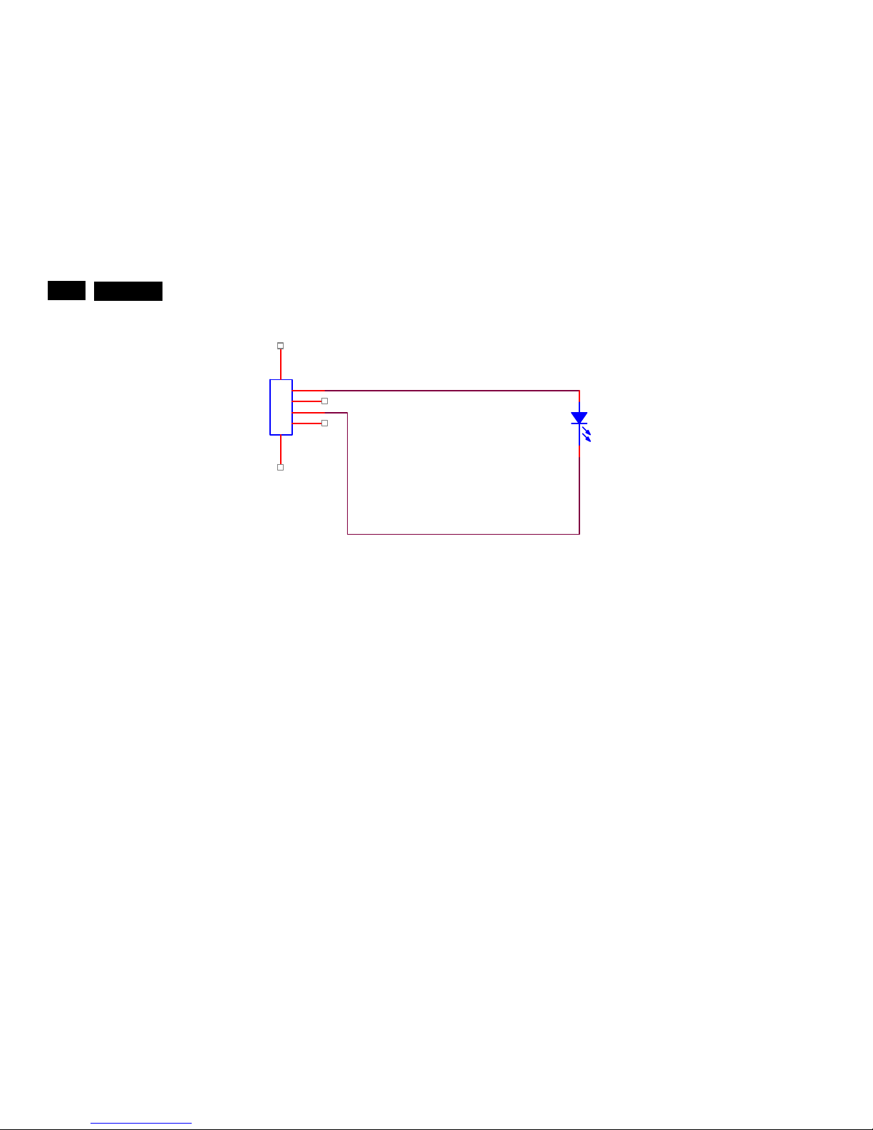
6.3 LED Board (715G3997T01000004F)
Remark: Parts position can be searched by using FIND function in PDF.
CN002
CONN
1
2
3
4
56
LED001
LED
12
25
Meridian 2
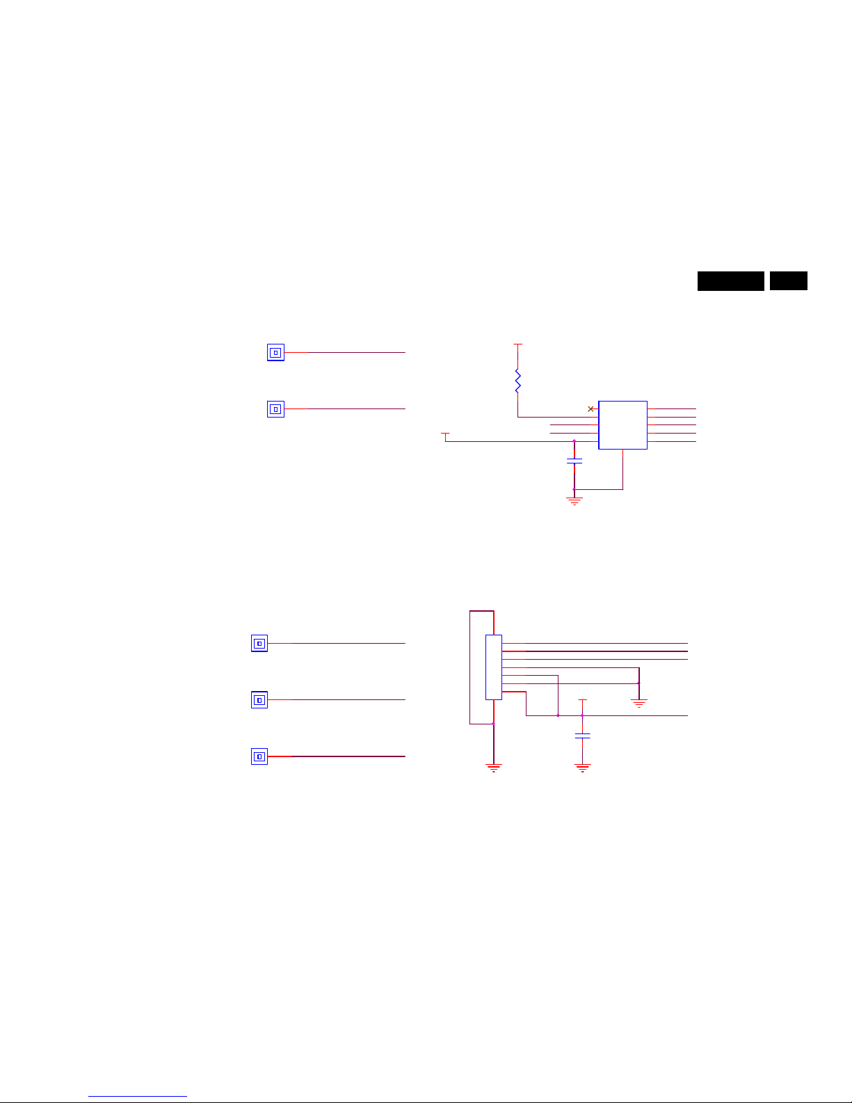
6.3 Key Board (715G3996K01000004S)
Remark: Parts position can be searched by using FIND function in PDF.
VCC3.3
I2C_SDA
C001
1uF Z 10V
CB005
CAPACI TIVE BUTTON
1
Brightness \ up
POWER
CS_5
I2C_SCL
I2C_SDA
CS_4
CN001
CONN
1
2
3
4
5
6
7
8 9
3.3V DC SW
U001
CAP1006-1-AIA-TR
1
2
3
4
5 6
7
8
9
10
11
CS1
ALERT
SDAT
SCLK
VDD CS6
CS5
CS4
CS3
CS2
GND
ECO \ Ba ck
C003
4.7UF 16V
CB003
CAPACI TIVE BUTTON
1
Sma rtImage \ down
CS_6
CS_3
VCC3.3
ALERT#
ALERT#
I2C_SCL
CS_6
CB004
CAPACI TIVE BUTTON
1
ALE
CS_2
CB002
CAPACI TIVE BUTTON
1 CS_2
CS_3
VCC3.3
CS_5
Menu \ OK
CB001
CAPACI TIVE BUTTON
1
R001
10K1/16W
CS_4
26
Meridian 2
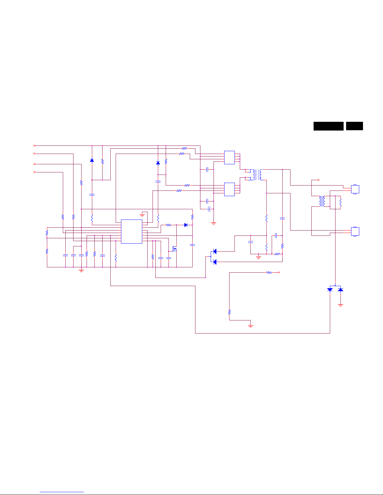
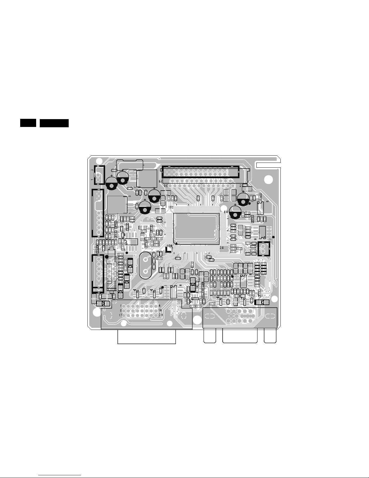
7. PCB Layout
7.1 Scaler Board (715G3737M0D0000H4K)
Remark: Parts position can be searched by using FIND function in PDF.
D101
FB404
FB401
FB402
FB403
FB407
U101
U402
U403
U701
R421
R105
R106
R107
R101
R111
R112
R113
R114
R115
R116
R123 R124
R125
R119
R120
R121
R126
R127
R128R129
R130
R131
R136
R132
R137
R138
R134
R133
R135
R139
R423
R406
R407
R401
R409
R411
R412
R413
R415
R416
R419
R420
R422
R424
R426
R429
R430
R441
R442
R438
R439
R702
R703
R704R706
C102
C103 C104
C105
C106 C107
C108
C109 C110
C111
C113
C112
C114
C116
C115
C117
C417
C403
C430
C405
C703
C407
C408
C704
C409
C410
C411
C412
C706
C707
C714
C401
C418
C420
C422
C717
C431
C432
C427
C709
C701
C708
D404
R404
R108
CN408
C101
R710
X401
R434
Q401
Q701
C434
C435
R402
R432
R431
R428
R427
R140
R709
C118
C119
C402
C436
R448
C419
C712
C433
CN403
CN701
U103
U104
U102
U107
U106
Q702
R721
R722
R449
Q703
C429
CN405
CN404
CN406
R414
R425
R433
U702
C713
U704
CN101
CN102
C705
C710
C711
U401
D401
D402
D403
ZD101
ZD102
CN407
CN402
CN401
C425
C426C428
C715
C718
C404
C413
C416
C421
C423
C702
C716
R102
R141
R403
R405
R435
R436
R437
R443
R444
R701
R708
R711R712
R713
R714
R715
R716
R717
R718
R719
R720
R723
R122
R417
FB405
FB406
FB408
FB409
Q704
U105
U703
D102Q101
Q402
Q706
Q707
C120R142
R451
R452
R724
R725
CN409
C414
R408
C406
C415
C424
R418
R103 R104
R109
R110
R117
R118
R410
R440
R446
C181
C182
R798
R799
Q705
C437
FB701
R707
27
Meridian 2

28
Meridian 2
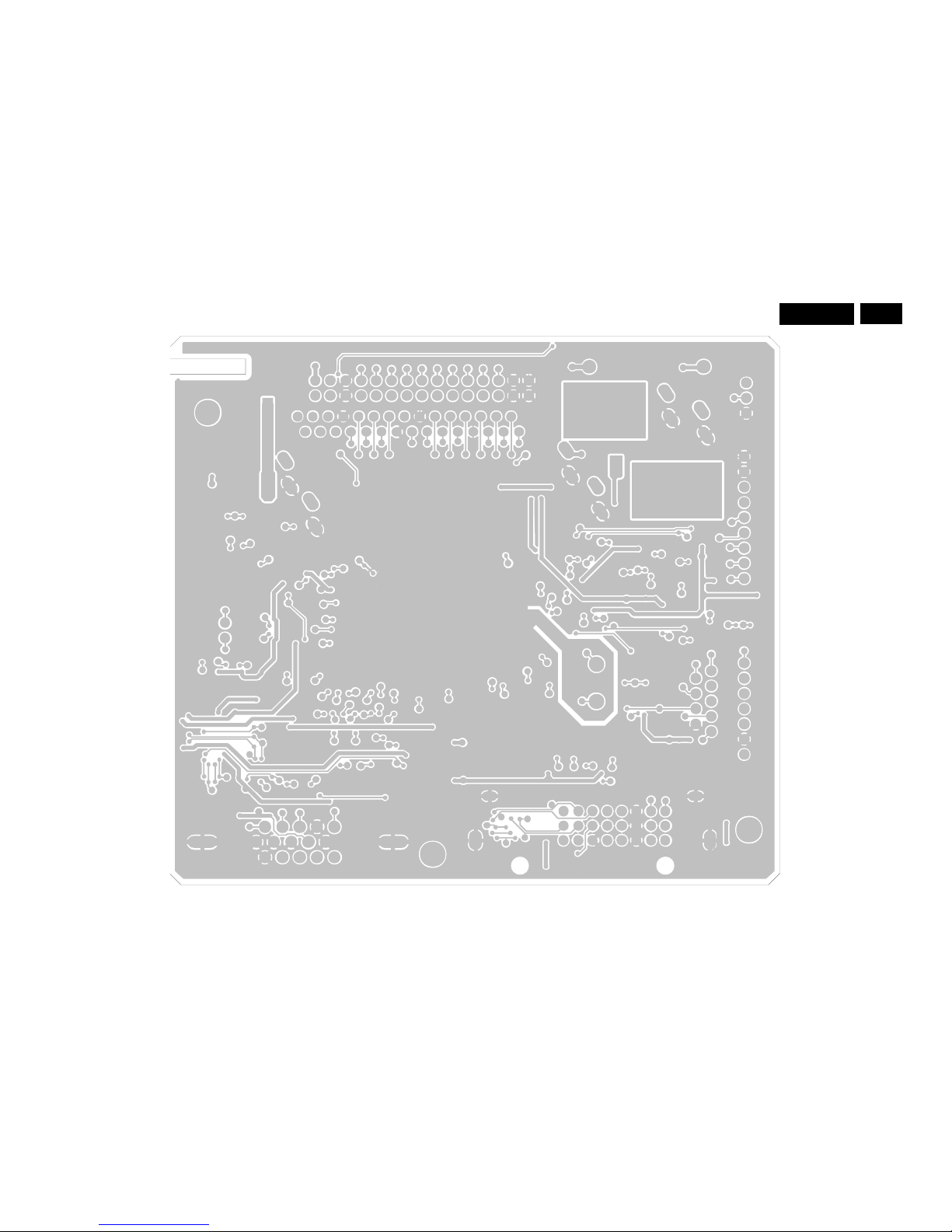
7.2 Power Board (715G3974P01000001S)
Remark: Parts position can be searched by using FIND function in PDF.
BD901
C604
C607
C614
C615
C804
C817
C819
C820
C821
C822
C900
C901
C902
C903
C907
C908
C909
C916
CN602
CN801
CN802
CN803
CN804
CN901
CN902
CN903
D601
D801
D802
D803
D901
D902
D903
D904D905
F901
F902
F903
FB601
FB602
FB901
GND2
IC601
IC903
IC904
L801
L802
L903
L904
L905
L906
PT801
Q903
R828
R904
R946
R947
ZD901
ZD902
SCR
SCR1
SCR2
D906
J621
J622
J804
J806
J815
J905
J813
J916
J828
J810
J623
J624
J902
J812
J817
J820
J908
J909
J914
J629
J630
J819
J803
J823
J807
J811
J918
J901
J919
C906
CN905
C905
J917
J903
C917
C918
FB902
CN902A
L901
T901
J904
GND1
NR901
CN603
CN604
R615
R613
C801
C802
C915
CN601
J625
IC901

29
Meridian 2
Remark: Parts position can be searched by using FIND function in PDF.
C601
C602
C603
C606
C608
C609
C610
C611
C612
C613
C620
C621
C805
C806
C810
C811
C812
C813
C814
C815
C818
C910
C912
C922
C923
C924
C929
C930
C931
C932
C935
D805
D806 D807
D808
IC801
Q607
Q608
Q802
Q805
Q806
R601
R602
R603
R604
R605
R606
R607
R608
R609
R610
R611
R612
R614
R616
R617
R618
R619
R620
R621
R625
R627
R628
R801
R802
R803
R804
R806
R807
R808
R809
R810
R811
R813
R815
R816
R817
R818
R819
R820
R821
R822
R823
R830
R836
R837
R838
R839
R840
R841
R842
R843
R844
R845
R901R902
R903
R906
R907
R908
R909
R911
R918
R919
R920
R924
R925
R926
R927 R930
R935
R939
R940
R943
R961
R962
RJ603
RJ601
RJ602
R812
R912
R910
R905
C808
C809
R913
RJ801
RJ802
RJ604
R626

30
Meridian 2
7.3 LED Board (715G3997T01000004F)
Remark: Parts position can be searched by using FIND function in PDF.
LED001
CN002

31
Meridian 2
7.4 Key Board (715G3996K01000004S)
Remark: Parts position can be searched by using FIND function in PDF.
CB1
CB2
CN20
CN21
C3
C1
CN001
R1
U1

32
Meridian 2
8. Wiring Diagram
Scaler Board
CN701
CN408
D-SUB
NT68668FG (U401)
9
1
CN404
7
1
Power Board
AC IN
1
7
CN901
CN902A
CN102
1
2
29
30
DVI
CN101
Key Board
CN802
CN803
Panel
1
7
CN001
CN002
41
LED Board
FFC Cable

33
Meridian 2
9. Scaler Board Overview
DC-DC
Scaler IC
D-SUB EEPROM
DVI EEPROM
Flash EEPROM

34
Meridian 2
10. Mechanical Instructions
Step 1: Remove the stand-base ass’y
1. Place the monitor face on a safe surface, and
remove the 4 screw covers.
2. Remove the 4 screws and then remove the stand
base ass’y from the monitor.
Step 2: Remove the rear cover
1. Open the latches and along the red arrowhead
direction as the picture to open other latches

35
Meridian 2
Step 3: Remove the bezel
1. Disconnect the connector and remove the screws to
remove the LED board.
2. Disconnect the connector to remove the key board.
Step 4: Remove the mainframe
1. Tear out all of the aluminum foils
2. Disconnect the connectors.
3. Press to release left and right latches of LVDS cable
and disconnect the LVDS cable.

36
Meridian 2
Step 5: Remove the boards
1. Remove the Main Board
2. Remove the Power Board
3. Disconnect all the connectors.

37
Meridian 2
11. Repair Flow Chart
1. No Power
OK
NG
No power
Check power cable is
tightened?
Check Power “On/Off”
is “On”?
Re-plug the power cable
Replace main board and check connections
Check the LED
indicator is OK?
Check the AC power
Replace the power board and check connections
OK
NG
OK
NG
NG
Turn on the Power “On/Off” switch
Replace key board and check connections
NG

38
Meridian 2
2.
Video (Power LED White)
17.
No Video (Power LED White)
Press the power
button is OK?
Check the LVDS/FFC
cable or panel
The end
NG
OK
OK
NG
Replace the main board
Replace the power
board and connection
Replace the LVDS/FFC
cable or panel
NG
The end
Replace the key board
NG
OK
Replace the main
board and connection
OK

39
Meridian 2
3.M
17.
OK
The end
OK
The end
OK
The end
DIM (image overlap, focus or flicker)
Reset in factory mode
Set to the optimal
frequency, select the
recommended fre
q
uenc
y
Pull out signal cable and
check “Self Test Feature
Check” is ok?
Check the signal cable
and the PC
Readjust the phase and pixel
clock in the user mode
Replace the main board
Replace the panel
NG
NG
NG
OK
NG
NG
OK
The end
OK
NG

40
Meridian 2
4. Color is not optimal
NG
Color is not optimal
Miss color
Color shift
Replace the signal cable
Pull out the signal cable
and check the screen
color display is normal?
The end
Replace the signal cable or PC
Reset the factory mode
In the user mode, set the” color
settings” until customer satisfy
Replace the main board
NG
OK
NG
OK
NG

41
Meridian 2
12. ISP Instruction
When do the parts, need the tools as follow:
A. An i486 (or above) personal computer or compatible.
B. Microsoft operation system Windows 95/98/2000/XP.
C. “PORT95NT” and “EasyUSB WriterV4.4” programs
D. ISP Board (715GT034-B) x1, Printer cablex1, VGA cable x1, 12V DC power source
12.1 Install the “PORT95NT” and “EasyUSB WriterV4.4” , and then restart the computer.
12.2. Connect the ISP board as follow:
12.3 The process of ISP writing as follows:
Connect to
the PC LPT
DC 12V Input
Connect this port to the
Philips model VGA port

42
Meridian 2
a. Double-click to running the program as follows:
b. Judge the monitor whether belong to “data in flash” or not, if belong to it, please click “option” item and select
“FE2P Mode Enable”, otherwise, don’t do any actions. Like as below picture:

43
Meridian 2
c. Click “option” and select “Setup ISP tool ”,
d. Select “NVT Type I (default)”, and then click the icon “Confirm Change”.

44
Meridian 2
e. Click icon, search the correct program, and then click open:
f. Click
icon. After display “Chip erase OK.”, “Programing Success”, “ISP OFF”, it means F/W updated OK,
it will show as the follow picture:

45
Meridian 2
13. DDC Instruction
General
DDC Data Re-programming
In case the main EEPROM with Software DDC which store all factory settings were replaced because a defect
repaired monitor’ the serial numbers have to be re-programmed.
It is advised to re- soldered the main EEPROM with Software DDC from the old board onto the new board if circuit
board have been replaced, in this case the DDC data does not need to be re-programmed.
Additional information about DDC (Display Data Channel) may be obtained from Video Electronics Standards
Association (VESA). Extended Display Identification Data (EDID) information may be also obtained from VESA.
1. An i486 (or above) personal computer or compatible.
2. Microsoft operation system Windows 95/98/2000/XP.
3. “PORT95NT.exe, TPVDDC5.6.exe” program.
4. EDID Board (715GT034-B) x1,
5. Printer cablex1, VGA cable x 1, DVI-D cable x 1, 12V DC power source
6. EDID data
13.1. Install the “PORT95NT.EXE”, and restart the computer.
The process of installing “PORT95NT” has been specified in, so it will not be specified again. If you have any
problem, please read it.
13.2 Connect the DDC Board as follow:
Note:
If the VGA is NG, please try to cut off the 5th pin of the VGA connector.
If the DVI is NG, please try to cut off the 14th pin of the DVI connector.
Connect to the PC LPT
Connect this port to the
Philips model VGA port
DC 12V Input
Connect this port to the
Philips model DVI-D port

46
Meridian 2
1. Rename the EDID data to “wa”, “wd”.
2. Put the “wa” and “wd” into a new folder, and then create another new folder named “ddc” (It must be “ddc” instead
of other names).
Step1: Must put the “ddc” folder, “TPVDDC5.6.exe” into the same folder.
Step2: Must copy EDID data and “config” to “ddc” folder.

47
Meridian 2
3. Double-click ,appear as follow:
4. Click “LoadFile”, it will show the picture as follow:

48
Meridian 2
5. Click “OK”, it will show the picture as follow:
6. Key in the same 14 numbers in the Input SN and Verify SN.

49
Meridian 2
7. Click “Program”, when the DDC Write complete, it will show the picture as follow:
8. Click “ReadBoth”, if the DDC Write is OK, it will show the picture as follow:

50
Meridian 2
220S2 EDID
Analog
00 01 02 03 04 05 06 07 08 09 0A 0B 0C 0D 0E 0F
-----------------------------------------------
00| 00 FF FF FF FF FF FF 00 41 0C 86 08 BD E6 04 00
10| 01 00 01 03 68 2F 1E 78 2A 78 F1 A6 55 48 9B 26
20| 12 50 54 B7 4B 00 81 80 95 00 95 0F B3 00 01 01
30| 01 01 01 01 01 01 21 39 90 30 62 1A 27 40 68 B0
40| 36 00 D9 28 11 00 00 1C 00 00 00 FF 00 32 33 31
50| 32 31 33 32 31 33 0A 20 20 20 00 00 00 FC 00 50
60| 68 69 6C 69 70 73 20 32 32 30 53 0A 00 00 00 FD
70| 00 38 4C 1E 53 11 00 0A 20 20 20 20 20 20 00 B7
EDID Structure Version/Revision: 01 03
<-Vendor/Product Identification: ->
ID Manufacturer Name: PHL
ID Product Code: 0886
ID Serial Number: 321213
Week of Manufacture: 1
Year of Manufacture: 1990
<-Basic Display Parameters/Features: ->
Video i/p definition: Analog
Max. H. Image Size: 47cm
Max. V. Image Size: 30cm
Display Gamma: 2.2
<-Color Characteristics: ->
Rx: 0.649 Gx: 0.283 Bx: 0.151 Wx: 0.313
Ry: 0.335 Gy: 0.605 By: 0.073 Wy: 0.329
<-Established Timings: ->
Established Timings 1:B7
720 x 400 @ 70Hz VGA, IBM
640 x 480 @ 60Hz VGA, IBM
640 x 480 @ 67Hz Apple, Mac II
640 x 480 @ 75Hz VESA
800 x 600 @ 56Hz VESA

51
Meridian 2
800 x 600 @ 60Hz VESA
Established Timings 2:4B
800 x 600 @ 75Hz VESA
1024 x 768 @ 60Hz VESA
1024 x 768 @ 75Hz VESA
1280 x1024 @ 75Hz VESA
Established Timings 3:00
<-Standard Timing Identification: ->
1280 x 1024 @ 60Hz
1440 x 900 @ 60Hz
1440 x 900 @ 75Hz
1680 x 1050 @ 60Hz
<-Detailed Timing Descriptions: ->
FC (Monitor Name): Philips 220S
FD (Monitor Limits):
Min. V. rate: 56 Hz
Max. V. rate: 76 Hz
Min. H. rate: 30 KHz
Max. H. rate: 83 KHz
Max. P Clock: 170 MHz
FF (Monitor SN): 231213213
Detailed Timing: 1680x1050 @ 60Hz
Extension Flag: 00
Block0 Checksum: B7

52
Meridian 2
Digital
00 01 02 03 04 05 06 07 08 09 0A 0B 0C 0D 0E 0F
-----------------------------------------------
00| 00 FF FF FF FF FF FF 00 41 0C 86 08 BD E6 04 00
10| 01 00 01 03 80 2F 1E 78 2A 78 F1 A6 55 48 9B 26
20| 12 50 54 B7 4B 00 81 80 95 00 95 0F B3 00 01 01
30| 01 01 01 01 01 01 21 39 90 30 62 1A 27 40 68 B0
40| 36 00 D9 28 11 00 00 1C 00 00 00 FF 00 32 33 31
50| 32 31 33 32 31 33 0A 20 20 20 00 00 00 FC 00 50
60| 68 69 6C 69 70 73 20 32 32 30 53 0A 00 00 00 FD
70| 00 38 4C 1E 53 11 00 0A 20 20 20 20 20 20 00 9F
EDID Structure Version/Revision: 01 03
<-Vendor/Product Identification: ->
ID Manufacturer Name: PHL
ID Product Code: 0886
ID Serial Number: 321213
Week of Manufacture: 1
Year of Manufacture: 1990
<-Basic Display Parameters/Features: ->
Video i/p definition: Digital
Max. H. Image Size: 47cm
Max. V. Image Size: 30cm
Display Gamma: 2.2
<-Color Characteristics: ->
Rx: 0.649 Gx: 0.283 Bx: 0.151 Wx: 0.313
Ry: 0.335 Gy: 0.605 By: 0.073 Wy: 0.329
<-Established Timings: ->
Established Timings 1:B7
720 x 400 @ 70Hz VGA, IBM
640 x 480 @ 60Hz VGA, IBM
640 x 480 @ 67Hz Apple, Mac II
640 x 480 @ 75Hz VESA
800 x 600 @ 56Hz VESA
800 x 600 @ 60Hz VESA

53
Meridian 2
Established Timings 2:4B
800 x 600 @ 75Hz VESA
1024 x 768 @ 60Hz VESA
1024 x 768 @ 75Hz VESA
1280 x1024 @ 75Hz VESA
Established Timings 3:00
<-Standard Timing Identification: ->
1280 x 1024 @ 60Hz
1440 x 900 @ 60Hz
1440 x 900 @ 75Hz
1680 x 1050 @ 60Hz
<-Detailed Timing Descriptions: ->
FC (Monitor Name): Philips 220S
FD (Monitor Limits):
Min. V. rate: 56 Hz
Max. V. rate: 76 Hz
Min. H. rate: 30 KHz
Max. H. rate: 83 KHz
Max. P Clock: 170 MHz
FF (Monitor SN): 231213213
Detailed Timing: 1680x1050 @ 60Hz
Extension Flag: 00
Block0 Checksum: 9F

54
Meridian 2
14. White Balance, Luminance Adjustment
1. Apparatuses and program: analyzer CA-210, PC, tool, FGA adjustment program (PHILIPS 220S2.DDCI),
Pattern generator.
2. Equipment installation:
a. Connect analyzer CA-210 to PC by USB connector, install drive program CA-SDK Ver4.00 for CA-210 and restart
PC after finish installing
b. Install Port95NT drive program, set PC printer connector mode as ECP mode and reset PC after finish installing.
c. Connect tool as follow:
Note: It’s not necessary to connect Port2.
3. Adjustment
Preparation before adjustment:
a. Monitor should be warmed up for more than half an hour.
b. Make sure that the tools are connected right and drive programs have been installed OK.
4. Adjustment process:
a. Press the power of CA-210, shut off the lens, press 0-Cal and open the lens after analyzer reset.
b. Open white balance adjustment program, select the right parameter according with the program and click OK.
c. Make sure that the lens of CA-210 aims at the center of the screen, then click START to adjust.
d. After finish adjusting, the adjustment program displays pass, and the START button changes for NEXT, which
means that you can adjust another monitor.
To PC LPT
To BSG-265A or
e
q
uivalent instrument
To PC Port 2 Philips 220S2

55
Meridian 2
5. Color Temp confirmation
Connect the signal to the monitor, the monitor displays white-picture, use CA-210 to measure the Color Temp of the
screen center and select the OSD to make sure whether the Color Temps accord with the SPEC.
6. How to enter into the factory mode:
Press the
and at the same time, and then DC ON/OFF, the picture will appear on the top left
corner. Choose “Input” item, and then choose “Factory”, you will enter into the factory mode.

56
Meridian 2
15. Monitor Exploded View

57
Meridian 2
16. Recommended & Spare Parts List
Recommended Parts for 220S2SB/00
Item Location PCM Codes Description Remark
1 FQ101 705GQA34048 BEZEL ASSY LGD
1 FQ101 705GQA34049 BEZEL ASSY SEC
2 FQ004 KEPC9QP4 KEY BOARD ASSY
3 FQ012 KEPC9QL4 KEY BOARD ASSY
4 E750 750GLG220W1P13M0PH PANEL LM220WE1-TLP1 GZ LGD
4 E750 750GLG220W1P13N000 PANEL LM220WE1-TLP1 GZ LGD
4 E750 750GLS220T05CCM0PH PANEL LTM220MT05 812 FQ SEC
4 E750 750GLS220T05CCN000 PANEL LTM220MT05 012 FQ SEC
4 E750 750GLS220T05DCM0PH PANEL LTM220MT05 813 FQ SEC
4 E750 750GLS220T05DCN000 PANEL LTM220MT05 013 FQ SEC
5 FQ003 PWPC9C21MYF1 POWER BOARD ASSY
6 FQ002 756GQ9CB PH009 00 SCALER BOARD ASSY(CBPC9NRPHQ3) LGD
6 FQ002 756GQ9CB PH010 00 SCALER BOARD ASSY(CBPC9NRPHQ3) SEC
7 FQ105 A34G1827ADT 1B0100 REAR COVER 22W LGD
7 FQ105 A34G1827ADT 2B0100 REAR_COVER 22w SEC
8 FQ103 705GQA34051 STAND BASE ASSY
E08902 089G 728HAA 2G SIGNAL CABLE
E08902 089G 728HAA 2G SIGNAL CABLE
E08901 089G404A18N CX AC POWER CORD 1800MM EUROPE Reg.
FQ415 0M1G1740 8120
SCREW FOR STD/MF
42-D020715/42-D000649()
FQ205 705GQACS006 CUSHION ASSY
FQ202 Q44GC133813 1A 22 PHILIPS LCD CARTON
FQ210 Q45G 88606 R PE BAG FOR BASE
FQ203 Q45G 88609206 N EPE BAG
E08907 S89G179T30N521 FFC CABLE
U402 100GPNGC004NT1 PHILIPS 220S2 LGD
U402 100GPNSC004NT1 PHILIPS 220S2(SEC) SEC
X401 093G 2251B J CRYSTAL 12MHZ NXS12.000AC30F-KAB10
U401 056G 562280 IC NT68668FG QFP-128
U701 056G 563149 IC G903T63UF 0.6A/3.3V SOT-223
U703 056G 563161 IC AME8815BEGT180Z 1.5A/1.8V SOT-223
U106 056G 662504 IC ESD AOZ8902CIL 24KV 5A SOT23-6 AOS
U107 056G 662504 IC ESD AOZ8902CIL 24KV 5A SOT23-6 AOS
U104 056G 662504 IC ESD AOZ8902CIL 24KV 5A SOT23-6 AOS
U103 056G 662504 IC ESD AOZ8902CIL 24KV 5A SOT23-6 AOS

58
Meridian 2
U102 056G 662504 IC ESD AOZ8902CIL 24KV 5A SOT23-6 AOS
IC903 056G 139 7 IC EL817MC M-TYPE
T901 080GL19P 11 S XFMR FOR POWER 650uH 10%
PT801 080GL20T 43 H INVERTER XFMR 80UH 12% 54D-9084
IC904 056G 158 12 KIA431A-AT/P TO-92
F901 084G 56 4 B FUSE 4A 250V
F903 084G 56 4 B FUSE 4A 250V
IC801 056G 608 12 IC ta9687GN-A-0-TR SOP-16
U1 056G 669 5 IC touch key CAP1006-1-AIA-TR QFN-10
Spare Parts for 220S2SB/93
Location PCM Codes Description Remark
E08903 089G1748CAA AC SIGNAL CABLE DVI COMLINK
E08903 089G1748HAA AC DVI CABLE
E08907 089G179W30N521 FFC CABLE
E08901 089G414A18N CX AC POWER CORD 1800MM China Regulation
E08901 089G414A18N IS AC POWER CORD 1800MM China Regulation
E09502 095G8014 7W939 HARNESS 7P-7P+4P 200mm+300mm WDK09112002
E09502 095G8014 7X939 HARNESS 7P-7P+4P 200mm+300mm LCDXXTF0397
FQ415 0M1G1740 8120 SCREW FOR STD/MF 42-D020715/42-D000649()
FQ101 705GQA34048 BEZEL ASSY
FQ103 705GQA34051 STAND BASE ASSY
E750 750GLG220W1P13M0PH PANEL LM220WE1-TLP1 GZ LGD
E750 750GLG220W1P13N000 PANEL LM220WE1-TLP1 GZ LGD
FQ124 A15G1137101 MAIN_FRAME
FQ105 A34G1827ADT 1B0100 REAR COVER 22W
FQ201 Q40G 22N81315A RATING LABEL
FQ206 Q41G78S1813 6A 220S2 QSG(non)
FQ205 705GQACS 44025 EPS ASSY
FQ202 Q44GC139813 1A 22 LCD CARTON
FQ210 Q45G 88606 R PE BAG FOR BASE
FQ203 Q45G 88609206 N EPE BAG
FQ210 Q70G22C1813 2A 220S2 CD MANUAL
E08907 S89G179T30N521 FFC CABLE
FQ003 PWPC9C21MYF1 POWER BOARD ASSY
GND1 009G6005 1 GROUND TERMINAL
CN803 033G8021 2E F WAFER
CN802 033G8021 2E F WAFER
CN802 033G8021 2E XY CONNECTOR
CN803 033G8021 2E XY CONNECTOR
IC903 056G 139 7 IC EL817MC M-TYPE
IC903 056G 139 11 IC TLP781F(D4-BLL,F) photocoupler DIP-4
NR901 061G 58100 X NTC10D2-14MC
NR901 061G 58100 WD RST NTCR 10 OHM +-20% 5A THINKING
C903 063G107K224 UM X2 CAP 0.22uF K 275VAC
C906 065G 1K103 2E6921 CAP CER 10NF K 1KV Y5U
C817 065G 6J2096ET 2PF 5% SL 6KV
C901 065G305M1022BP Y2 1000PF M 250VAC Y5P
C902 065G305M1022BP Y2 1000PF M 250VAC Y5P
C900 065G306M3322B3 0.0033UF/250V
C905 067G 40Z10115K
CAP 105℃ 100UF M 450V

59
Meridian 2
C905 067G 40Z10115L EC 100uF 450V M 18*36mm
C916 067G204V102 2C CAP CS 1000UF 20% 10V 10*12
C916 067G204V102 2K CAP CS 1000UF 20% 10V 10*12
C908 067G215R2207KV LOW ESR EC 22uF 50V M 6.3*11mm
C915 067G215S4713KV
EC 105℃ CAP 470UF M 16V
C915 067G215S4713LV LOW ESR EC 470uF 16V M 10*12.5mm
C918 067G215S6814KV
CAP 105℃ 680uF M 25V
C917 067G215S6814KV
CAP 105℃ 680uF M 25V
C804 067G215S6814KV
CAP 105℃ 680uF M 25V
C917 067G215S6814LV LOW ESR EC 680uF 25V M 12.5*16mm
C918 067G215S6814LV LOW ESR EC 680uF 25V M 12.5*16mm
C804 067G215S6814LV LOW ESR EC 680uF 25V M 12.5*16mm
C908 067G215Y2207LV EC 22UF 20% 50V RZW 6.3*11
C909 067G315Y4707KV LOW ESR EC 47uF M 50V 6.3*11mm
C909 067G315Y4707LV LOW ESR EC 47uF M 50V 6.3*11mm
L801 073G 174 63 HA IND FILTER 150mH DADON
L801 073G 174 63DNA LINE FILTER BY DARFON LK.3711D.101
L901 073G 174 65 H2 LINE FILTER 30mH MIN
L901 073G 174 65 S2 LINE FILTER 30mH MIN
L904 073G 253 91 H CHOKE COIL
L903 073G 253 91 H CHOKE COIL
L904 073G 253 91 HP CHOKE COIL 3.5uH VOC
L903 073G 253 91 HP CHOKE COIL 3.5uH VOC
T901 080GL19P 11 N XFMR FOR POWER 650uH 10%
T901 080GL19P 11 S XFMR FOR POWER 650uH 10%
PT801 080GL20T 43 H INVERTER XFMR 80UH 12% 54D-9084
PT801 080GL20T 43 DN INVERTER XFMR 73uH TK.2009Y.101
CN901 087G 501 32 S AC SOCKET
CN901 087G 501 32 DL AC SOCKET DIP 3PIN+2PIN GROUND
BD901 093G 50460 51 BRIDGE D2SB80 2A/800V GBL
D903 093G 60272 DIODE_5A/40V_SR540
D904 093G 60272 DIODE_5A/40V_SR540
D903 093G 60923 DIODE SR504-30 DO-201AD
D904 093G 60923 DIODE SR504-30 DO-201AD
CN902A 095G 820 7D902 HARNESS 7P(SAN)-9P 200mm FQE91817I
CN902A 095G 820 7X902 HARNESS 7P(SAN)-9P 200mm LCDXXTF0409
T901 S80GL19P11V XFMR FOR POWER 1.295mH 10% TPV-PT
IC901 056G 379181 IC AC/DC TOP266EG eSIP-7C
HS1 Q90G0203 1 HEAT SINK
D906 093G 60903 Diode MBRF10150CT TSC
HS3 Q90G6264 5 HEAT SINK
IC801 056G 608 12 IC ta9687GN-A-0-TR SOP-16
Q806 057G 600928 MOSFET AO4614BL SO-8
Q805 057G 600928 MOSFET AO4614BL SO-8
Q802 057G 759 2A TANSISTOR 2N7002 SOT-23
Q805 057G 763 61 FET AO4614 SO-8
Q806 057G 763 61 FET AO4614 SO-8
Q806 057G 763111 FET APM4568AKC-TRG 40V/6.5A SOP-8
Q805 057G 763111 FET APM4568AKC-TRG 40V/6.5A SOP-8
R820 061G0603100 JY RST CHIPR 10OHM 1/10W YAGEO
R821 061G0603100 JY RST CHIPR 10OHM 1/10W YAGEO
R926 061G06031001FT RST CHIP 1K 1/10W 1%
R927 061G06031002FT RST CHIP 10K 1/10W 1%
R806 061G06031003FT RST CHIP 100K 1/10W 1%
R801 061G0603103 JT RST CHIP 10K 1/10W 5% TZAI YUAN
R807 061G0603103 JT RST CHIP 10K 1/10W 5% TZAI YUAN
R813 061G0603104 JT RST CHIP 100K 1/10W 5% TZAI YUAN

60
Meridian 2
R809 061G0603105 JY RST CHIP 1M 1/10W 5% YAGEO
R815 061G0603153 JF RST CHIPR 15KOHM 5% 1/10W FENGHUA
R808 061G06033900FY RST CHIPR 390 OHM +-1% 1/10W YAGEO
R842 061G0603471 JT RST CHIPR 470OHM +-5% 1/10W TZAI YUAN
R838 061G0603471 JY RST CHIPR 470 OHM 5% 1/10W YAGEO
R836 061G0603563 JY RST CHIPR 56KOHM +-5% 1/10W YAGEO
R837 061G0603752 JF RST CHIPR 7.5KOHM 5% 1/10W FENGHUA
R811 061G06038202FY RST CHIPR 82KOHM +-1% 1/10W YAGEO
R810 061G06039102FF RST CHIPR 91KOHM +-1% 1/10W FENGHUA
R930 061G06039531FF RST CHIPR 9.53KOHM +-1% 1/10W FENGHUA
RJ802 061G0805000 JF RST CHIPR 0 OHM +-5% 1/8W FENGHUA
R906 061G0805100 JF RST CHIPR 10 OHM +-5% 1/10W FENGHUA
R906 061G0805100 JY RST CHIPR 10OHM +- 5% 1/8W YEGAO
R939 061G08051001FT RST CHIP 1K 1/8W 1%
R939 061G08051001FY RST CHIPR 1KOHM +-1% 1/8W YAGEO
R812 061G08051003FY RST CHIPR 100KOHM +-1% 1/8W YAGEO
R802 061G0805221 JT RST CHIP 220R 1/8W 5% TZAI YUAN
R816 061G0805229 JF RST CHIPR 2R2 +-5% 1/8W FENGHUA
R817 061G0805229 JF RST CHIPR 2R2 +-5% 1/8W FENGHUA
R818 061G0805229 JF RST CHIPR 2R2 +-5% 1/8W FENGHUA
R819 061G0805229 JF RST CHIPR 2R2 +-5% 1/8W FENGHUA
R924 061G0805471 JF RST CHIPR 470 OHM +-5% 1/8W FENGHUA
R943 061G0805471 JT RST CHIPR 470OHM +-5% 1/8W TZAI YUAN
R803 061G0805512 JI TEST ONLY RST 5.1K OHM 5% 1/8W TA-I
R804 061G0805512 JI TEST ONLY RST 5.1K OHM 5% 1/8W TA-I
R830 061G0805682 JF RST CHIPR 6.8KOHM +-5% 1/8W FENGHUA
R903 061G0805689 JF RST CHIPR 6R8 +-5% 1/8W FENGHUA
R908 061G08058871FF RST CHIPR 8.87K OHM+-1% 1/8W FENGHUA
R911 061G08059102FY RST CHIPR 91KOHM +-1% 1/8W YAGEO
R912 061G12060004JF RST CHIPR MAX0R05 4A 1/4W FENGHUA
R962 061G1206101 JT RST CHIPR 100 OHM +-5% 1/4W TZAI YUAN
R961 061G1206101 JT RST CHIPR 100 OHM +-5% 1/4W TZAI YUAN
R935 061G1206101 JT RST CHIPR 100 OHM +-5% 1/4W TZAI YUAN
R920 061G1206101 JT RST CHIPR 100 OHM +-5% 1/4W TZAI YUAN
R919 061G1206101 JT RST CHIPR 100 OHM +-5% 1/4W TZAI YUAN
R918 061G1206101 JT RST CHIPR 100 OHM +-5% 1/4W TZAI YUAN
R910 061G1206103 JF RST CHIPR 10KOHM +-5% 1/4W FENGHUA
R901 061G1206105 JF RST CHIPR 1 MOHM +-5% 1/4W FENGHUA
R902 061G1206105 JF RST CHIPR 1 MOHM +-5% 1/4W FENGHUA
R902 061G1206105 JT RST CHIPR 1MOHM +-5% 1/4W TZAI YUAN
R901 061G1206105 JT RST CHIPR 1MOHM +-5% 1/4W TZAI YUAN
C932 065G060310232K Y CAP CHIP 0603 1N 50V X7R +/-10%
C814 065G060322131J F CAP CHIP 0603 220PF J 50V NPO
C805 065G060322332K Y CAP CHIP 0603 22N 50V X7R +/-10%
C810 065G060333232K 3 CAP CHIP 0603 3300pF K 50V X7R
C923 065G080510432K Y CAP CHIP 0805 100N 50V X7R +/-10%
C815 065G080510432K Y CAP CHIP 0805 100N 50V X7R +/-10%
C811 065G080510432K Y CAP CHIP 0805 100N 50V X7R +/-10%
C924 065G080510432K Y CAP CHIP 0805 100N 50V X7R +/-10%
C931 065G080510432K Y CAP CHIP 0805 100N 50V X7R +/-10%
C818 065G080515522K 3 CAP 0805 1.5UF +/-5% 25V X7R TDK
C809 065G080522131J Y CAP CHIP 0805 220P 50V NPO +/-5%
C806 065G080522512K T CAP CHIP 0805 2.2UF K 16V X7R
C808 065G080533332K M CAP 0805 33NF K 50V X7R
C935 065G1206102B2K M CAP CHIP 1206 1000pF 630V X7R
C929 065G1206102B2K M CAP CHIP 1206 1000pF 630V X7R

61
Meridian 2
C912 065G1206102B2K M CAP CHIP 1206 1000pF 630V X7R
C910 065G1206102B2K M CAP CHIP 1206 1000pF 630V X7R
D806 093G 64 42 P BAV70 SOT23 BY PAN JIT
D805 093G 6433P BAV99
CN901 006G 31500 EYELET
PT801 006G 31502 1.5MM RIVET
IC904 056G 158 12 KIA431A-AT/P TO-92
Q903 057G 761 16 TRA KTD1028 KEC
R904 061G152M10452T RST MOFR 100KOHM +-5% 2WS
R946 061G152M47152T RST MOFR 470 OHM +-5% 2WS
R947 061G152M47152T RST MOFR 470 OHM +-5% 2WS
R828 061G212Y62552T SY RST MGFR 6.2MOHM +-5% 1/2W FUTABA
C907 065G 2K152 2T6921 CAP CER 1500pF K 2KV Y5P
C801 065G500K4732GT CAP JC 47NF 10% 50V X7R
C802 065G500K4732GT CAP JC 47NF 10% 50V X7R
FB902 071G 55 9 T FERRITE BEAD
FB901 071G 55 29 FERRITE BEAD
F901 084G 56 4 B FUSE 4A 250V
F903 084G 56 4 B FUSE 4A 250V
ZD901 093G 3916852T MTZJ T-72 22B
ZD902 093G 3958152T HZ24-2
ZD901 093G 39A6852T ZENER DIODES MTZJ22B DO-34
D901 093G 6026T52T RECTIFIER DIODE FR107
D902 093G 6038T52T FR103
D803 093G 64 1152T 1N4148
D802 093G 64 1152T 1N4148
D801 093G 64 1152T 1N4148
FQ002 756GQ9CB PH009 00 SCALER BOARD ASSY(CBPC9NRPHQ3)
U402 100GPNGC004NT1 MCU ASSY(056G1133 90 1)
CN404 033G3802 7B Y CONNECTOR 7P 2.0 DIP
CN701 033G3802 9B Y CONNECTOR 9P 2.0
CN701 033G3802 9B Y W WAFER
CN408 033G801930F CH L FFC CONNECTOR 30P 1.0pitch
CN408 033G801930F CH JS CONNECTOR
R707 061G152M479 64 SH RST MOFR 4.7 OHM +-5% 2WS SANHUAN
R707 061G152M479 64 SY RST MOFR 4.7 OHM +-5% 2WS FUTABA
CN101 088G 35315F HD D-SUB CONN F ATTACHED SCREW
CN101 088G 35315F XH D-SUB 15PIN VERTICAL CONN WITH SCREW
CN102 088G 35424F HN DVI CONN + SHIELD 24P F WITH SCREW
CN102 088G 35424FXNH DVI CONN + SHIELD 24P F WITH SCREW
X401 093G 2251B J CRYSTAL 12MHZ NXS12.000AC30F-KAB10
C716 067G 3051007PB EC 10UF 20% 50V 5*11
C705 067G 3051013PB
EC 105℃ 100uF M 16V 5*11mm
C702 067G 3051013PB
EC 105℃ 100uF M 16V 5*11mm
C433 067G 3051013PB
EC 105℃ 100uF M 16V 5*11mm
C433 067G 3051013XB EC 100UF 20% 16V 5*11
C705 067G 3051013XB EC 100UF 20% 16V 5*11
C702 067G 3051013XB EC 100UF 20% 16V 5*11
C710 067G 4051013PB EC 100uF M 16V 5*11mm
U401 056G 562280 IC NT68668FG QFP-128
U701 056G 563149 IC G903T63UF 0.6A/3.3V SOT-223
U703 056G 563161 IC AME8815BEGT180Z 1.5A/1.8V SOT-223
U106 056G 662 13 IC AZC099-04S SOT23-6L
U104 056G 662 13 IC AZC099-04S SOT23-6L
U103 056G 662 13 IC AZC099-04S SOT23-6L
U102 056G 662 13 IC AZC099-04S SOT23-6L
U107 056G 662 13 IC AZC099-04S SOT23-6L

62
Meridian 2
U102 056G 662504 IC ESD AOZ8902CIL 24KV 5A SOT23-6 AOS
U103 056G 662504 IC ESD AOZ8902CIL 24KV 5A SOT23-6 AOS
U104 056G 662504 IC ESD AOZ8902CIL 24KV 5A SOT23-6 AOS
U106 056G 662504 IC ESD AOZ8902CIL 24KV 5A SOT23-6 AOS
U107 056G 662504 IC ESD AOZ8902CIL 24KV 5A SOT23-6 AOS
U402 056G1133 90 1 IC PM25LV020-100SCE 2MB SOIC-8 PMC
U105 056G1133918 IC AT24C02BN-SH-T 8-SOIC
U101 056G1133918 IC AT24C02BN-SH-T 8-SOIC
U101 056G1133956 IC CAT24C02WI-GT3 SO-8
U105 056G1133956 IC CAT24C02WI-GT3 SO-8
Q701 057G 417 12 T KEC 2N3904S-RTK/PS
Q706 057G 417 12 T KEC 2N3904S-RTK/PS
Q401 057G 417 13 T KEC 2N3906S-RTK/PS
Q402 057G 417 13 T KEC 2N3906S-RTK/PS
Q401 057G 417517 TRA LMBT3906LT1G -200mA/-40V SOT-23 LRC
Q402 057G 417517 TRA LMBT3906LT1G -200mA/-40V SOT-23 LRC
Q701 057G 417518 TRA LMBT3904LT1G 200mA/40V SOT-23 LRC
Q706 057G 417518 TRA LMBT3904LT1G 200mA/40V SOT-23 LRC
Q705 057G 763940 MOSFET AO3401A SOT-23
R103 061G0402000 JI TEST ONLY RST 0402 0.05R MAX 1/16W TA-I
R104 061G0402000 JI TEST ONLY RST 0402 0.05R MAX 1/16W TA-I
R109 061G0402000 JI TEST ONLY RST 0402 0.05R MAX 1/16W TA-I
R110 061G0402000 JI TEST ONLY RST 0402 0.05R MAX 1/16W TA-I
R117 061G0402000 JI TEST ONLY RST 0402 0.05R MAX 1/16W TA-I
R118 061G0402000 JI TEST ONLY RST 0402 0.05R MAX 1/16W TA-I
R414 061G0402000 JI TEST ONLY RST 0402 0.05R MAX 1/16W TA-I
R409 061G0402000 JI TEST ONLY RST 0402 0.05R MAX 1/16W TA-I
R103 061G0402000 JT RST CHIPR MAX0R05 1/16W TZAI YUAN
R104 061G0402000 JT RST CHIPR MAX0R05 1/16W TZAI YUAN
R109 061G0402000 JT RST CHIPR MAX0R05 1/16W TZAI YUAN
R110 061G0402000 JT RST CHIPR MAX0R05 1/16W TZAI YUAN
R117 061G0402000 JT RST CHIPR MAX0R05 1/16W TZAI YUAN
R118 061G0402000 JT RST CHIPR MAX0R05 1/16W TZAI YUAN
R414 061G0402000 JT RST CHIPR MAX0R05 1/16W TZAI YUAN
R409 061G0402000 JT RST CHIPR MAX0R05 1/16W TZAI YUAN
R134 061G0402100 JI TEST ONLY RST 0402 10R 5% 1/16W TA-I
R135 061G0402100 JI TEST ONLY RST 0402 10R 5% 1/16W TA-I
R136 061G0402100 JI TEST ONLY RST 0402 10R 5% 1/16W TA-I
R137 061G0402100 JI TEST ONLY RST 0402 10R 5% 1/16W TA-I
R138 061G0402100 JI TEST ONLY RST 0402 10R 5% 1/16W TA-I
R139 061G0402100 JI TEST ONLY RST 0402 10R 5% 1/16W TA-I
R140 061G0402100 JI TEST ONLY RST 0402 10R 5% 1/16W TA-I
R141 061G0402100 JI TEST ONLY RST 0402 10R 5% 1/16W TA-I
R141 061G0402100 JT RST CHIP 10R 1/16W 5% TZAI YUAN
R140 061G0402100 JT RST CHIP 10R 1/16W 5% TZAI YUAN
R139 061G0402100 JT RST CHIP 10R 1/16W 5% TZAI YUAN
R138 061G0402100 JT RST CHIP 10R 1/16W 5% TZAI YUAN
R137 061G0402100 JT RST CHIP 10R 1/16W 5% TZAI YUAN
R136 061G0402100 JT RST CHIP 10R 1/16W 5% TZAI YUAN
R135 061G0402100 JT RST CHIP 10R 1/16W 5% TZAI YUAN
R134 061G0402100 JT RST CHIP 10R 1/16W 5% TZAI YUAN
R439 061G0402101 JI TEST ONLY RST 0402 100R 5% 1/16W TA-I
R431 061G0402101 JI TEST ONLY RST 0402 100R 5% 1/16W TA-I
R421 061G0402101 JI TEST ONLY RST 0402 100R 5% 1/16W TA-I
R129 061G0402101 JI TEST ONLY RST 0402 100R 5% 1/16W TA-I
R128 061G0402101 JI TEST ONLY RST 0402 100R 5% 1/16W TA-I

63
Meridian 2
R127 061G0402101 JI TEST ONLY RST 0402 100R 5% 1/16W TA-I
R124 061G0402101 JI TEST ONLY RST 0402 100R 5% 1/16W TA-I
R123 061G0402101 JI TEST ONLY RST 0402 100R 5% 1/16W TA-I
R119 061G0402101 JI TEST ONLY RST 0402 100R 5% 1/16W TA-I
R113 061G0402101 JI TEST ONLY RST 0402 100R 5% 1/16W TA-I
R111 061G0402101 JI TEST ONLY RST 0402 100R 5% 1/16W TA-I
R108 061G0402101 JI TEST ONLY RST 0402 100R 5% 1/16W TA-I
R106 061G0402101 JI TEST ONLY RST 0402 100R 5% 1/16W TA-I
R105 061G0402101 JI TEST ONLY RST 0402 100R 5% 1/16W TA-I
R102 061G0402101 JI TEST ONLY RST 0402 100R 5% 1/16W TA-I
R101 061G0402101 JI TEST ONLY RST 0402 100R 5% 1/16W TA-I
R121 061G0402101 JI TEST ONLY RST 0402 100R 5% 1/16W TA-I
R123 061G0402101 JT RST CHIP 100R 1/16W 5% TZAI YUAN
R124 061G0402101 JT RST CHIP 100R 1/16W 5% TZAI YUAN
R127 061G0402101 JT RST CHIP 100R 1/16W 5% TZAI YUAN
R128 061G0402101 JT RST CHIP 100R 1/16W 5% TZAI YUAN
R129 061G0402101 JT RST CHIP 100R 1/16W 5% TZAI YUAN
R421 061G0402101 JT RST CHIP 100R 1/16W 5% TZAI YUAN
R431 061G0402101 JT RST CHIP 100R 1/16W 5% TZAI YUAN
R439 061G0402101 JT RST CHIP 100R 1/16W 5% TZAI YUAN
R121 061G0402101 JT RST CHIP 100R 1/16W 5% TZAI YUAN
R119 061G0402101 JT RST CHIP 100R 1/16W 5% TZAI YUAN
R113 061G0402101 JT RST CHIP 100R 1/16W 5% TZAI YUAN
R111 061G0402101 JT RST CHIP 100R 1/16W 5% TZAI YUAN
R108 061G0402101 JT RST CHIP 100R 1/16W 5% TZAI YUAN
R106 061G0402101 JT RST CHIP 100R 1/16W 5% TZAI YUAN
R105 061G0402101 JT RST CHIP 100R 1/16W 5% TZAI YUAN
R102 061G0402101 JT RST CHIP 100R 1/16W 5% TZAI YUAN
R101 061G0402101 JT RST CHIP 100R 1/16W 5% TZAI YUAN
R130 061G0402102 JF RST CHIPR 1KOHM +-5% 1/16W FENGHUA
R703 061G0402102 JF RST CHIPR 1KOHM +-5% 1/16W FENGHUA
R130 061G0402102 JI TEST ONLY RST 0402 1K 5% 1/16W TA-I
R703 061G0402102 JI TEST ONLY RST 0402 1K 5% 1/16W TA-I
R425 061G0402103 JI TEST ONLY RST 0402 10K 5% 1/16W TA-I
R799 061G0402103 JI TEST ONLY RST 0402 10K 5% 1/16W TA-I
R721 061G0402103 JI TEST ONLY RST 0402 10K 5% 1/16W TA-I
R714 061G0402103 JI TEST ONLY RST 0402 10K 5% 1/16W TA-I
R704 061G0402103 JI TEST ONLY RST 0402 10K 5% 1/16W TA-I
R702 061G0402103 JI TEST ONLY RST 0402 10K 5% 1/16W TA-I
R444 061G0402103 JI TEST ONLY RST 0402 10K 5% 1/16W TA-I
R429 061G0402103 JI TEST ONLY RST 0402 10K 5% 1/16W TA-I
R425 061G0402103 JT RST CHIP 10K 1/16W 5% TZAI YUAN
R799 061G0402103 JT RST CHIP 10K 1/16W 5% TZAI YUAN
R721 061G0402103 JT RST CHIP 10K 1/16W 5% TZAI YUAN
R714 061G0402103 JT RST CHIP 10K 1/16W 5% TZAI YUAN
R704 061G0402103 JT RST CHIP 10K 1/16W 5% TZAI YUAN
R702 061G0402103 JT RST CHIP 10K 1/16W 5% TZAI YUAN
R444 061G0402103 JT RST CHIP 10K 1/16W 5% TZAI YUAN
R429 061G0402103 JT RST CHIP 10K 1/16W 5% TZAI YUAN
R415 061G0402104 JI TEST ONLY RST 0402 100K 5% 1/16W TA-I
R422 061G0402104 JI TEST ONLY RST 0402 100K 5% 1/16W TA-I
R427 061G0402104 JI TEST ONLY RST 0402 100K 5% 1/16W TA-I
R415 061G0402104 JT RST CHIP 100K 1/16W 5% TZAI YUAN
R422 061G0402104 JT RST CHIP 100K 1/16W 5% TZAI YUAN
R427 061G0402104 JT RST CHIP 100K 1/16W 5% TZAI YUAN
R432 061G0402105 JF RST CHIPR 1MOHM 5% 1/16W FENGHUA
R432 061G0402105 JI TEST ONLY RST 0402 1M 5% 1/16W TA-I

64
Meridian 2
R420 061G04021200FF RST CHIPR 120 OHM +-1% 1/16W FENGHUA
R420 061G04021200FT RST CHIP 120R 1/16W 1% TZAI YUAN
R126 061G0402222 JI TEST ONLY RST 0402 2.2K 5% 1/16W TA-I
R125 061G0402222 JI TEST ONLY RST 0402 2.2K 5% 1/16W TA-I
R411 061G0402222 JI TEST ONLY RST 0402 2.2K 5% 1/16W TA-I
R125 061G0402222 JT RST CHIP 2K2 1/16W 5% TZAI YUAN
R126 061G0402222 JT RST CHIP 2K2 1/16W 5% TZAI YUAN
R411 061G0402222 JT RST CHIP 2K2 1/16W 5% TZAI YUAN
R719 061G0402223 JI TEST ONLY RST 0402 22K 5% 1/16W TA-I
R701 061G0402223 JI TEST ONLY RST 0402 22K 5% 1/16W TA-I
R133 061G0402223 JI TEST ONLY RST 0402 22K 5% 1/16W TA-I
R116 061G0402223 JI TEST ONLY RST 0402 22K 5% 1/16W TA-I
R719 061G0402223 JT RST CHIP 22K 1/16W 5% TZAI YUAN
R701 061G0402223 JT RST CHIP 22K 1/16W 5% TZAI YUAN
R133 061G0402223 JT RST CHIP 22K 1/16W 5% TZAI YUAN
R116 061G0402223 JT RST CHIP 22K 1/16W 5% TZAI YUAN
R423 061G0402224 JF RST CHIPR 220KOHM +-5% 1/16W FENGHUA
R416 061G0402224 JF RST CHIPR 220KOHM +-5% 1/16W FENGHUA
R416 061G0402224 JT RST CHIP 220K 1/16W 5% TZAI YUAN
R423 061G0402224 JT RST CHIP 220K 1/16W 5% TZAI YUAN
R406 061G0402331 JT RST CHIP 330R 1/16W 5% TZAI YUAN
R407 061G0402331 JT RST CHIP 330R 1/16W 5% TZAI YUAN
R424 061G0402331 JT RST CHIP 330R 1/16W 5% TZAI YUAN
R419 061G0402394 JF RST CHIP R 390K +/-5% 1/16W FENGHUA
R419 061G0402394 JY RST CHIP R 390K +/-5% 1/16W YAGEO
R408 061G04024700FF RST CHIP 470R 1/16W 1% FENGHUA
R408 061G04024700FT RST CHIP 470R 1/16W 1%
R142 061G0402471 JI TEST ONLY RST 0402 470R 5% 1/16W TA-I
R142 061G0402471 JT RST CHIP 470R 1/16W 5% TZAI YUAN
R114 061G0402472 JI TEST ONLY RST CHIP 4.7K 5% 1/16W TA-I
R115 061G0402472 JI TEST ONLY RST CHIP 4.7K 5% 1/16W TA-I
R132 061G0402472 JI TEST ONLY RST CHIP 4.7K 5% 1/16W TA-I
R131 061G0402472 JI TEST ONLY RST CHIP 4.7K 5% 1/16W TA-I
R132 061G0402472 JT RST CHIP 4K7 1/16W 5% TZAI YUAN
R131 061G0402472 JT RST CHIP 4K7 1/16W 5% TZAI YUAN
R115 061G0402472 JT RST CHIP 4K7 1/16W 5% TZAI YUAN
R114 061G0402472 JT RST CHIP 4K7 1/16W 5% TZAI YUAN
R715 061G0402563 JF RST CHIPR 56KOHM 1/16W FENGHUA
R715 061G0402563 JT RST CHIPR 56KOHM 1/16W TZAI YUAN
R107 061G04027509FI TEST ONLY RST 0402 75R 1% 1/16W TA-I
R112 061G04027509FI TEST ONLY RST 0402 75R 1% 1/16W TA-I
R120 061G04027509FI TEST ONLY RST 0402 75R 1% 1/16W TA-I
R107 061G04027509FT RST CHIP 75R 1/16W 1%
R112 061G04027509FT RST CHIP 75R 1/16W 1%
R120 061G04027509FT RST CHIP 75R 1/16W 1%
R122 061G0603000 JI TEST ONLY RST 0603 0.05R MAX 1/16W TA-I
R122 061G0603000 JT RST CHIP MAX 0R05 1/10W TZAI YUAN
R417 061G0603101 JI TEST ONLY RST 0603 100R 5% 1/16W TA-I
R417 061G0603101 JT RST CHIP 100R 1/10W 5% TZAI YUAN
R418 061G0603821 JF RST CHIPR 820 OHM +- 5% 1/10W FENGHUA
R418 061G0603821 JT RST CHIP 820R 1/10W 5% TZAI YUAN
R449 061G1206221 JI TEST ONLY RST 220 OHM 5% 1/4W TA-I
R448 061G1206221 JI TEST ONLY RST 220 OHM 5% 1/4W TA-I
R449 061G1206221 JT RST CHIPR 220 OHM +-5% 1/4W TZAI YUAN
R448 061G1206221 JT RST CHIPR 220 OHM +-5% 1/4W TZAI YUAN
C120 065G040210232K 3 CHIP 1000pF 50V X7R

65
Meridian 2
C120 065G040210232K A CAP 0402 1NF K 50V X7R
C410 065G040210232K T CAP CHIP 0402 1000PF 50V X7R
C410 065G040210232K Y CAP CHIP 0402 1N 50V X7R +/-10%
C707 065G040210425K 3 CAP CHIP 0402 100N 25V X5R +/-10%
C706 065G040210425K 3 CAP CHIP 0402 100N 25V X5R +/-10%
C704 065G040210425K 3 CAP CHIP 0402 100N 25V X5R +/-10%
C703 065G040210425K 3 CAP CHIP 0402 100N 25V X5R +/-10%
C701 065G040210425K 3 CAP CHIP 0402 100N 25V X5R +/-10%
C434 065G040210425K 3 CAP CHIP 0402 100N 25V X5R +/-10%
C427 065G040210425K 3 CAP CHIP 0402 100N 25V X5R +/-10%
C425 065G040210425K 3 CAP CHIP 0402 100N 25V X5R +/-10%
C422 065G040210425K 3 CAP CHIP 0402 100N 25V X5R +/-10%
C419 065G040210425K 3 CAP CHIP 0402 100N 25V X5R +/-10%
C409 065G040210425K 3 CAP CHIP 0402 100N 25V X5R +/-10%
C408 065G040210425K 3 CAP CHIP 0402 100N 25V X5R +/-10%
C407 065G040210425K 3 CAP CHIP 0402 100N 25V X5R +/-10%
C405 065G040210425K 3 CAP CHIP 0402 100N 25V X5R +/-10%
C403 065G040210425K 3 CAP CHIP 0402 100N 25V X5R +/-10%
C402 065G040210425K 3 CAP CHIP 0402 100N 25V X5R +/-10%
C401 065G040210425K 3 CAP CHIP 0402 100N 25V X5R +/-10%
C119 065G040210425K 3 CAP CHIP 0402 100N 25V X5R +/-10%
C118 065G040210425K 3 CAP CHIP 0402 100N 25V X5R +/-10%
C117 065G040210425K 3 CAP CHIP 0402 100N 25V X5R +/-10%
C115 065G040210425K 3 CAP CHIP 0402 100N 25V X5R +/-10%
C114 065G040210425K 3 CAP CHIP 0402 100N 25V X5R +/-10%
C113 065G040210425K 3 CAP CHIP 0402 100N 25V X5R +/-10%
C417 065G040210425K 3 CAP CHIP 0402 100N 25V X5R +/-10%
C713 065G040210425K 3 CAP CHIP 0402 100N 25V X5R +/-10%
C712 065G040210425K 3 CAP CHIP 0402 100N 25V X5R +/-10%
C418 065G040210425K 3 CAP CHIP 0402 100N 25V X5R +/-10%
C703 065G040210425K T CAP CHIP 0402 0.1uF 25V X5R
C704 065G040210425K T CAP CHIP 0402 0.1uF 25V X5R
C401 065G040210425K T CAP CHIP 0402 0.1uF 25V X5R
C119 065G040210425K T CAP CHIP 0402 0.1uF 25V X5R
C118 065G040210425K T CAP CHIP 0402 0.1uF 25V X5R
C117 065G040210425K T CAP CHIP 0402 0.1uF 25V X5R
C713 065G040210425K T CAP CHIP 0402 0.1uF 25V X5R
C712 065G040210425K T CAP CHIP 0402 0.1uF 25V X5R
C707 065G040210425K T CAP CHIP 0402 0.1uF 25V X5R
C706 065G040210425K T CAP CHIP 0402 0.1uF 25V X5R
C113 065G040210425K T CAP CHIP 0402 0.1uF 25V X5R
C114 065G040210425K T CAP CHIP 0402 0.1uF 25V X5R
C115 065G040210425K T CAP CHIP 0402 0.1uF 25V X5R
C701 065G040210425K T CAP CHIP 0402 0.1uF 25V X5R
C405 065G040210425K T CAP CHIP 0402 0.1uF 25V X5R
C407 065G040210425K T CAP CHIP 0402 0.1uF 25V X5R
C408 065G040210425K T CAP CHIP 0402 0.1uF 25V X5R
C409 065G040210425K T CAP CHIP 0402 0.1uF 25V X5R
C417 065G040210425K T CAP CHIP 0402 0.1uF 25V X5R
C403 065G040210425K T CAP CHIP 0402 0.1uF 25V X5R
C402 065G040210425K T CAP CHIP 0402 0.1uF 25V X5R
C418 065G040210425K T CAP CHIP 0402 0.1uF 25V X5R
C419 065G040210425K T CAP CHIP 0402 0.1uF 25V X5R
C422 065G040210425K T CAP CHIP 0402 0.1uF 25V X5R
C425 065G040210425K T CAP CHIP 0402 0.1uF 25V X5R
C427 065G040210425K T CAP CHIP 0402 0.1uF 25V X5R
C434 065G040210425K T CAP CHIP 0402 0.1uF 25V X5R

66
Meridian 2
C437 065G0402105A5K 3 CAP CHIP 0402 1UF K 10V X5R
C420 065G0402105A5K 3 CAP CHIP 0402 1UF K 10V X5R
C424 065G0402105A5K A CAP CHIP 0402 1UF K 10V X5R
C415 065G0402105A5K A CAP CHIP 0402 1UF K 10V X5R
C414 065G0402105A5K A CAP CHIP 0402 1UF K 10V X5R
C406 065G0402105A5K A CAP CHIP 0402 1UF K 10V X5R
C406 065G0402105A5K T CAP CHIP 0402 1uF K 10V X5R
C414 065G0402105A5K T CAP CHIP 0402 1uF K 10V X5R
C415 065G0402105A5K T CAP CHIP 0402 1uF K 10V X5R
C424 065G0402105A5K T CAP CHIP 0402 1uF K 10V X5R
C420 065G0402105A5K Y CAP 0402 1UF K 10V X5R
C437 065G0402105A5K Y CAP 0402 1UF K 10V X5R
C181 065G040222031J F CAP 0402 22PF J 50V NPO
C182 065G040222031J F CAP 0402 22PF J 50V NPO
C428 065G040222031J T CAP CHIP 0402 22PF 50V NPO
C426 065G040222031J T CAP CHIP 0402 22PF 50V NPO
C182 065G040222031J Y CAP CHIP 0402 22P 50V NPO +/-5%
C181 065G040222031J Y CAP CHIP 0402 22P 50V NPO +/-5%
C718 065G040222417Z T CAP CHIP 0402 0.22UF 16V Y5V
C715 065G040222417Z T CAP CHIP 0402 0.22UF 16V Y5V
C429 065G040222417Z T CAP CHIP 0402 0.22UF 16V Y5V
C116 065G040222417Z T CAP CHIP 0402 0.22UF 16V Y5V
C101 065G040222417Z T CAP CHIP 0402 0.22UF 16V Y5V
C101 065G040222417Z Y CAP CHIP 0402 220nF 16V Y5V
C116 065G040222417Z Y CAP CHIP 0402 220nF 16V Y5V
C429 065G040222417Z Y CAP CHIP 0402 220nF 16V Y5V
C715 065G040222417Z Y CAP CHIP 0402 220nF 16V Y5V
C718 065G040222417Z Y CAP CHIP 0402 220nF 16V Y5V
C110 065G040247312K A 8.31HIP 0402 47nF K 16V X7R
C108 065G040247312K A 8.31HIP 0402 47nF K 16V X7R
C107 065G040247312K A 8.31HIP 0402 47nF K 16V X7R
C105 065G040247312K A 8.31HIP 0402 47nF K 16V X7R
C104 065G040247312K A 8.31HIP 0402 47nF K 16V X7R
C102 065G040247312K A 8.31HIP 0402 47nF K 16V X7R
C102 065G040247312K T CAP CHIP 0402 0.047uF 16V X7R
C104 065G040247312K T CAP CHIP 0402 0.047uF 16V X7R
C105 065G040247312K T CAP CHIP 0402 0.047uF 16V X7R
C107 065G040247312K T CAP CHIP 0402 0.047uF 16V X7R
C108 065G040247312K T CAP CHIP 0402 0.047uF 16V X7R
C110 065G040247312K T CAP CHIP 0402 0.047uF 16V X7R
C102 065G040247317Z Y CAP CHIP 0402 47nF Z 17V Y5V
C104 065G040247317Z Y CAP CHIP 0402 47nF Z 17V Y5V
C105 065G040247317Z Y CAP CHIP 0402 47nF Z 17V Y5V
C107 065G040247317Z Y CAP CHIP 0402 47nF Z 17V Y5V
C108 065G040247317Z Y CAP CHIP 0402 47nF Z 17V Y5V
C110 065G040247317Z Y CAP CHIP 0402 47nF Z 17V Y5V
C103 065G040250931C 3 CAP CHIP 0402 5PF 50V NPO +/-0.25pF
C106 065G040250931C 3 CAP CHIP 0402 5PF 50V NPO +/-0.25pF
C109 065G040250931C 3 CAP CHIP 0402 5PF 50V NPO +/-0.25pF
C404 065G0805475A2K 3 CAP CHIP 4.7UF 10V X7R +/- 10%
C413 065G0805475A2K 3 CAP CHIP 4.7UF 10V X7R +/- 10%
C416 065G0805475A2K 3 CAP CHIP 4.7UF 10V X7R +/- 10%
C421 065G0805475A2K 3 CAP CHIP 4.7UF 10V X7R +/- 10%
C423 065G0805475A2K 3 CAP CHIP 4.7UF 10V X7R +/- 10%
C423 065G0805475A2K T CAP CHIP 4U7 10V X7R 10%
C421 065G0805475A2K T CAP CHIP 4U7 10V X7R 10%

67
Meridian 2
C416 065G0805475A2K T CAP CHIP 4U7 10V X7R 10%
C413 065G0805475A2K T CAP CHIP 4U7 10V X7R 10%
C404 065G0805475A2K T CAP CHIP 4U7 10V X7R 10%
FB409 071G 56K121 CHIP BEAD
FB409 071G 56K121 M CHIP BEAD
FB406 071G 56V301 B CHIP BEAD FCM2012VF-301T07 BULLWILL
FB701 071G 56V301 B CHIP BEAD FCM2012VF-301T07 BULLWILL
FB408 071G 56V301 B CHIP BEAD FCM2012VF-301T07 BULLWILL
FB405 071G 56V301 B CHIP BEAD FCM2012VF-301T07 BULLWILL
FB404 071G 56V301 B CHIP BEAD FCM2012VF-301T07 BULLWILL
FB403 071G 56V301 B CHIP BEAD FCM2012VF-301T07 BULLWILL
FB402 071G 56V301 B CHIP BEAD FCM2012VF-301T07 BULLWILL
FB401 071G 56V301 B CHIP BEAD FCM2012VF-301T07 BULLWILL
FB401 071G 56V301 M CHIP BEAD 2012 300 OHM
FB402 071G 56V301 M CHIP BEAD 2012 300 OHM
FB403 071G 56V301 M CHIP BEAD 2012 300 OHM
FB404 071G 56V301 M CHIP BEAD 2012 300 OHM
FB405 071G 56V301 M CHIP BEAD 2012 300 OHM
FB406 071G 56V301 M CHIP BEAD 2012 300 OHM
FB408 071G 56V301 M CHIP BEAD 2012 300 OHM
FB701 071G 56V301 M CHIP BEAD 2012 300 OHM
D102 093G 64 42 L DIODE LBAV70LT1G SOT-23 LRC
D101 093G 64 42 L DIODE LBAV70LT1G SOT-23 LRC
D101 093G 64 42 P BAV70 SOT23 BY PAN JIT
D102 093G 64 42 P BAV70 SOT23 BY PAN JIT
D402 093G 39GA01 T RLZ5.6B
D403 093G 39GA01 T RLZ5.6B
ZD102 093G 39GA01 T RLZ5.6B
ZD101 093G 39GA01 T RLZ5.6B
ZD101 093G 39S 24 T RLZ 5.6B LLDS
ZD102 093G 39S 24 T RLZ 5.6B LLDS
D403 093G 39S 24 T RLZ 5.6B LLDS
D402 093G 39S 24 T RLZ 5.6B LLDS
FQ012 KEPC9QL4 LIGHT BOARD ASSY
CN002 033G8032 4F S HR CONNECTOR
LED001 081G 63W 2 GP LED GPTS06033W-L5D 0603 WHITE
FQ004 KEPC9QP4 KEY BOARD ASSY
CN001 033G8032 7F S HR CONNECTOR 7P 1.25
U1 056G 669 5 IC touch key CAP1006-1-AIA-TR QFN-10
R1 061G0402103 JY RST CHIPR 10KOHM +-5% 1/16W YAGEO
C1 065G0402105A7Z Y CAP CHIP 0402 1uF Z 10V Y5V
C3 065G080547515K T CAP CHIP 0805 4.7UF K 16V X5R
FQ101 705GQA34049 BEZEL ASSY SEC
E750 750GLS220T05CCM0PH PANEL LTM220MT05 812 FQ SEC
E750 750GLS220T05CCN000 PANEL LTM220MT05 A12,812 FQ SEC
E750 750GLS220T05DCM0PH PANEL LTM220MT05 813 FQ SEC
E750 750GLS220T05DCN000 PANEL LTM220MT05 A13,813 FQ SEC
FQ124 A15G1137201 MAINFRAME
FQ105 A34G1827ADT 2B0100 REAR_COVER 22W SEC
FQ002 756GQ9CB PH010 00 SCALER BOARD ASSY(CBPC9NRPHQ3) SEC
U402 100GPNSC004NT1 MCU ASSY(056G1133 90 1) SEC

68
Meridian 2
Service Kit
Description Part No. Picture
DDC KIT
715GT034-B
NOVATEK ISP KIT

69
Meridian 2
17. Different Parts List
Diversity of 220S2SB/27 compared with 220S2SB/00
220S2SB/27 220S2SB/00
Location PCM Codes Description Location PCM Codes Description
E08901 089G402A18N CX AC POWER CORD 1800MM AMERICA REG. E08901 089G404A18N CX AC POWER CORD 1800MM EUROPE Reg.
Diversity of 220S2SB/69 compared with 220S2SB/00
220S2SB/69 220S2SB/00
Location PCM Codes Description Location PCM Codes Description
E08901 089G410A18N CX AC POWER CORD 1800mm UK Reg. E08901 089G404A18N CX AC POWER CORD 1800MM EUROPE Reg.
Diversity of 220S2SB/73 compared with 220S2SB/00
220S2SB/73 220S2SB/00
Location PCM Codes Description Location PCM Codes Description
Diversity of 220S2SB/75 compared with 220S2SB/00
220S2SB/75 220S2SB/00
Location PCM Codes Description Location PCM Codes Description
FQ301 089G412A18NIS3 POWER CORD/32E1818058 E08901 089G404A18N CX AC POWER CORD 1800MM EUROPE Reg.

70
Meridian 2
Diversity of 220S2CB/00 compared with 220S2SB/00
220S2CB/00 220S2SB/00
Location PCM Codes Description Location PCM Codes Description
FQ101 705GQA34065 BEZEL ASSY for LGD FQ101 705GQA34048 BEZEL ASSY for LGD
FQ101 705GQA34066 BEZEL ASSY for SEC FQ101 705GQA34049 BEZEL ASSY for SEC
FQ110 Q37G0199011 HINGE 22 FQ110 A37G0156011 HINGE
FQ109 A34G1983ADT 1B0100 BASE P1 FQ103 705GQA34051 STAND BASE ASSY
Diversity of 220S2CB/27 compared with 220S2SB/00
220S2CB/27 220S2SB/00
Location PCM Codes Description Location PCM Codes Description
Diversity of 220S2CB/69 compared with 220S2SB/00
220S2CB/69 220S2SB/00
Location PCM Codes Description Location PCM Codes Description
FQ101 705GQA34065 BEZEL ASSY for LGD FQ101 705GQA34048 BEZEL ASSY for LGD
FQ101 705GQA34066 BEZEL ASSY for SEC FQ101 705GQA34049 BEZEL ASSY for SEC
FQ109 A34G1983ADT 1B0100 BASE P1 FQ103 705GQA34051 STAND BASE ASSY
FQ205 705GQACS 44032 EPS ASSY FQ205 705GQACS006 CUSHION ASSY
FQ202 Q44GC145813 1A 22 LCD CARTON FQ202 Q44GC133813 1A 22 PHILIPS LCD CARTON

71
Meridian 2
Diversity of 220S2CB/75 compared with 220S2SB/00
220S2CB/75 220S2SB/00
Location PCM Codes Description Location PCM Codes Description
FQ301 089G412A18NIS3 POWER CORD/32E1818058 E08901 089G410A18N CX AC POWER CORD 1800mm UK Reg.
FQ101 705GQA34065 BEZEL ASSY for LGD FQ101 705GQA34048 BEZEL ASSY for LGD
FQ101 705GQA34066 BEZEL ASSY for SEC FQ101 705GQA34049 BEZEL ASSY for SEC
FQ109 A34G1983ADT 1B0100 BASE P1 FQ103 705GQA34051 STAND BASE ASSY
FQ205 705GQACS 44032 EPS ASSY FQ205 705GQACS006 CUSHION ASSY
FQ202 Q44GC145813 1A 22 LCD CARTON FQ202 Q44GC133813 1A 22 PHILIPS LCD CARTON
Diversity of 220S2SS/00 compared with 220S2SB/00
220S2SS/00 220S2SB/00
Location PCM Codes Description Location PCM Codes Description
FQ101 705GQA34104 BEZEL ASSY (LGD) FQ101 705GQA34048 BEZEL ASSY
FQ101 705GQA34103 BEZEL ASSY (SEC) FQ101 705GQA34049 BEZEL ASSY

72
Meridian 2
18. General Product Specification
Blue: Changes than last version
Red: TBD
. ANALOG AND DIGITAL (optional) DUAL INPUT
. AUTO PICTURE ADJUSTMENT
. 36 Support Timing and 14 PRESET Timing which can be recovered to PRESET MODES, 10 User MODES
. USER FRIENDLY OSD DISPLAY FOR MODE IDENTIFICATION /ADJUSTMENT
. MAX. RESOLUTION 1680 x 1050 NON-INTERLACED AT 60 Hz (VGA)
. 22″ COLOR TFT LCD FLAT PANEL
. FULL RANGE POWER SUPPLY 90 – 264 VAC
. CE ENVIRONMENTAL POLICY
. ANTI-GLARE TO REDUCE LIGHT REFLECTION
. POWER MANAGEMENT CAPABILITY
. SOG SUPPORT
. Windows Vista Premium Logo Certification
. HDCP support
. SMART CONTROL & SMART MANAGEMENT REQUIREMENT
. SMARTContrast 500K: 1 (Typical) Waiting for supplier input
. SMART Image
. SMART Response
. PrefectTune II (formerly FGA, FACTORY GAMMA Alignment)
. PHILIPS LOGO displayed while power on
. WEEE REQUIREMENT
. RoHS REQUIREMENT
. TCO5.0 REQUIREMENT

73
Meridian 2
CONTENTS
1 FOREWORD .................................................................................................................................................. 74
2 PRODUCT PROFILE ..................................................................................................................................... 74
2.1 S
CANNING FREQUENCIES
......................................................................................................................... 75
2.2 A
MBIENT TEMPERATURE
: ......................................................................................................................... 75
3 ELECTRICAL CHARACTERISTICS ............................................................................................................. 75
3.1 I
NTERFACE SIGNALS
................................................................................................................................ 75
3.2 I
NTERFACE
.............................................................................................................................................. 76
3.3 T
IMING REQUIREMENT
.............................................................................................................................. 77
3.4 H
ORIZONTAL SCANNING
........................................................................................................................... 78
3.5 V
ERTICAL SCANNING
................................................................................................................................ 78
3.6 P
OWER INPUT CONNECTION
..................................................................................................................... 78
3.7 P
OWER MANAGEMENT
............................................................................................................................. 78
3.8 VGA
DISPLAY IDENTIFICATION
.................................................................................................................. 79
3.9 DVI
DISPLAY IDENTIFICATION
................................................................................................................... 79
3.10 USB
SUPPORT ( NOT REQUIRED IN
220S2) ............................................................................................... 79
3.11 DDC
/CI S
UPPORT AND SMART MANAGE/CONTROL
................................................................................. 79
3.12 H
OT-KEY DEFINITION
................................................................................................................................ 79
3.13 S
MART CONTRAST (DYNAMIC CONTRAST RATIO
) ....................................................................................... 79
3.14 S
MART IMAGE
.......................................................................................................................................... 79
3.15 P
ERFECTTUNE
........................................................................................................................................ 81
4 VISUAL CHARACTERISTICS ....................................................................................................................... 82
4.1 T
EST CONDITIONS
.................................................................................................................................... 82
4.2 B
RIGHTNESS
........................................................................................................................................... 82
4.3 I
MAGE SIZE
.............................................................................................................................................. 82
4.4 B
RIGHTNESS UNIFORMITY
........................................................................................................................ 82
4.5 C
HECK CROSS TALK
(S) .......................................................................................................................... 82
4.6 C
OLOR TEMPERATURE ADJUSTMENT
......................................................................................................... 82
5 MECHANICAL CHARACTERISTICS ........................................................................................................... 83
5.1 C
OSMETIC
- ............................................................................................................................................. 83
5.2 M
ECHANICAL DATA FILES
- ....................................................................................................................... 83
5.3 L
OCATION OF PHILIPS LOGO
- ................................................................................................................... 83
5.4 G
AP BETWEEN PANEL AND FRONT BEZEL
.................................................................................................. 83
5.5 L
OCATION OF CONTROL ICONS
- ............................................................................................................... 84
5.6 C
OLOR FOR RESIN/PAINT
- ........................................................................................................................ 84
5.7 F
IRE ENCLOSURE REQUEST
...................................................................................................................... 84
5.8 R
ESINS
................................................................................................................................................... 84
5.9 I
F PAINT IS USED
...................................................................................................................................... 84
5.10 P
LASTIC MOLD TOOLING
........................................................................................................................... 84
5.11 P
LASTICS FLAMMABILITY
......................................................................................................................... 84
5.12 T
EXTURE/GLOSSING OF HOUSING
............................................................................................................. 84
5.13 T
ILT AND SWIVEL BASE
............................................................................................................................. 84
5.14 K
ENSINGTON LOCK
................................................................................................................................. 84
5.15 L
ABEL
..................................................................................................................................................... 85
5.16 P
RODUCT DIMENSION / WEIGHT ( REFER TO PHILIPS APPROVED
SHT 191/SHT560 ) ................................. 85
5.17 T
RANSPORTATION
.................................................................................................................................... 85
5.18 P
ALLET / CONTAINER LOADING (REFER TO PHILIPS APPROVED
SHT 560) .................................................. 85
6 ENVIRONMENTAL CHARACTERISTICS..................................................................................................... 86
6.1 S
USCEPTIBILITY OF DISPLAY TO EXTERNAL ENVIRONMENT
......................................................................... 86
6.2 T
RANSPORTATION TESTS
......................................................................................................................... 86
6.3 D
ISPLAY DISTURBANCES FROM EXTERNAL ENVIRONMENT
.......................................................................... 86
6.4 D
ISPLAY DISTURBANCES TO EXTERNAL ENVIRONMENT
............................................................................... 86
7 RELIABILITY ................................................................................................................................................. 86
7.1 M
EAN TIME BETWEEN FAILURES
............................................................................................................... 86
8 QUALITY ASSURANCE REQUIREMENTS .................................................................................................. 87
8.1 A
CCEPTANCE TEST
.................................................................................................................................. 87
9 PHILIPS’ FLAT PANEL MONITORS PIXEL DEFECT POLICY .................................................................... 87
10 REGULATORY COMPLIANCE ................................................................................................................. 89
10.1 W
ORLDWIDE REGULATORY
...................................................................................................................... 89
10.2 EMC
REQUIREMENTS
.............................................................................................................................. 89
10.3 R
O
HS ..................................................................................................................................................... 89
10.4 WEEE .................................................................................................................................................... 89
10.5 O
NGOING REGULATORY
........................................................................................................................... 89

74
Meridian 2
1. FOREWORD
This specification describes a 22″ WSXGA+ multi-scan color TFT LCD monitor with maximum resolution up to 1680
x 1050 /60 Hz non-interlaced. This model uses 250nits panel.
All optical characteristics are determined according to panel specification after warming up longer than 30 minutes.
2. PRODUCT PROFILE
2.1 EDID header
1 User visible strings on .inf file Philips 220S (22inch Wide LCD MONITOR 220S2)
2 Manufacturer ID ( EDID data) PHL
3 Product ID, "xxxx" 4 codes MSB(byte 12): 08
LSB (byte 11): 86
4 maximum resolution 1680 x1050
5 Horizontal Frequency Range 30~83 KHz
6 Vertical Frequency Range 56~76Hz
7 Monitor Name (13 characters max.) Philips 220S
* Detail timing descriptor in DVI EDID: Reduced blanking 1680 x1050 x60Hz
2.2 LCD
Suppliers to offer panel specifications.
Panel incoming specification: Follow Philips’ specification.
SEC
Type NR. : SEC LTM220MT05
Resolution : 1680 x 1050 (WSXGA+)
Outside dimensions : 493.7(H) x 320.1(V) Typ. x 17.0(D) Max.
Pitch (mm) : 0.282mm x 0.282mm
Color pixel arrangement : RGB vertical stripe
Display surface : Haze 25% hard coating (3H)
Color depth : 16.7M (6 bit Hi-FRC)
Backlight : 2 CCFL
Active area (W x H) : 473.76(H) x 296.1(V) mm
View angle (CR=10) : =160 for Right/Left (typ.)
: =160 for Up/Down (typ.)
Contrast ratio : 600:1(Min) 1000:1 (typ.)
White luminance : 200(Min) 250(typ.)
Color gamut : >=72%
Gate IC : ----
Source IC : SEC
Response time : Tr + Tf <=5 ms (typ.)
Vertical frequency range : 53~76Hz
LGD
Type NR. : LGD LM220WE1-TLP1
Resolution : 1680 x 1050 (WSXGA+)
Outside dimensions : 493.7(H) x 320.1 (V) x 14.5(D) mm (typ.)
Pitch (mm) : 0.282mm x 0.282mm
Color pixel arrangement : 1680 horizontal by 1050 vertical Pixels. RGB stripe arrangement
Display surface : Hard coating (3H), Anti-glare treatment of the front polarizer
Color depth : 16.7M colors

75
Meridian 2
Backlight : 2 CCFL
Active area (W x H) : 21.995 inches (558.673mm) diagonal (Aspect ratio 16:10)
View angle (CR>=10) : R/L 170(Typ.), U/D 160(Typ.)
Contrast ratio : 700:1(Min) 1000:1 (Typ.)
White luminance : 200cd/m2 (Min) 250 cd/m2 (Typ. Center 1 point)
Color gamut : >=72%
Gate IC : -----
Source IC : Lusem
Response time : <=5 ms (Typ.)
Vertical frequency range : 50~75Hz
2.3 Scanning Frequencies
Hor. : 30 - 83 K Hz
Ver. : 56 - 76 Hz
Video dot rate: < 165 MHz for VGA and < 170 MHz for DVI, warning message must be displayed
while over 165 MHz (supplier to provide accurate scaler bandwidth number)
Power input: 90-264 V AC, 50/60 ± 2 Hz
Power consumption:
On mode: < 30W (max.), 24W (typ.)
EPA 5.0 spec. < 29.7 watt
EPA 5.0 measure data < 24 watt
SmartImage ECO mode: <wtt
Functions:
(1) D-SUB analog R/G/B separate inputs, H/V sync separated, Composite (H+V) TTL level, SOG
sync
(2) DVI digital Panel Link TMDS inputs, HDCP supported.
2.4 Ambient temperature: 0 °C - 40 °C
3. ELECTRICAL CHARACTERISTICS
Scaler should be capable of below items.
1) Scaler must support color engine for Image enhancement feature (SmartImage)
2) Scaler must have enough memory to support PerfecTune feature and Philips OSD
3) Scaler must support SmartContras, 500K: 1 DCR preferred
4) Can be shared with 220S2
3.1 Interface signals
1). D-Sub Analog
Input signal : Video, Hsync, Vsync
Video : 0.7 Vp-p, input impedance, 75 ohm @DC
Sync. : Separate sync TTL level, input impedance 2.2k ohm terminate
Hsync Positive/Negative
Vsync Positive/Negative
Composite sync TTL level, input impedance 2.2k ohm terminate (Positive/Negative)
Sync on green video 0.3 Vp-p Negative (Video 0.7 Vp-p Positive)
2). DVI-D Digital
Input signal: Single TMDS link (Three channels: RX0-/+, RX1-/+, RX2-/+)

76
Meridian 2
3). USB PLUG 2.0 (not required in 220S2)
USB port (1 upstream, 1 downstream)
4). Audio (not required in 220S2)
Input signal: 1000 mVrms
Loudspeaker: 1W+ 1W stereo of RMS Power
Frequency range: (WAIT FOR SUPPLIER INPUT)
Headphone connection will mute speakers
3.2 Interface
3.2.1 D-Sub Cable
Length : 1.8 M +/- 50 mm
Fix with monitor when packing, with transplant pin protective cover.
Connector type : D-Sub male with DDC2B pin assignments.
Blue connector thumb-operated jack screws
Pin assignments:
PIN No. SIGNAL
1 Red
2 Green/ SOG
3 Blue
4 Sense (GND)
5 Cable Detect (GND)
6 Red GND
7 Green GND
8 Blue GND
9 DDC +3.3V or +5V
10 Logic GND
11 Sense (GND)
12 Bi-directional data
13 H/H+V sync
14 V-sync
15 Data clock
3.2.2 DVI Cable
The input signals are applied to the display through DVI-D cable.
Length : 1.8 M +/- 50 mm
Connector type : DVI-D male with DDC-2B pin assignments
White connector thumb-operated jackscrews
With transplant pin protective cover.
Pin Assignment:
Pin No. Description
1 T.M.D.S. data22 T.M.D.S. data2+
3 T.M.D.S. data2 shield

77
Meridian 2
4 No Connect
5 No Connect
6 DDC clock
7 DDC data
8 No Connect
9 T.M.D.S. data1-
10 T.M.D.S. data1+
11 T.M.D.S. data1 shield
12 No Connect
13 No Connect
14 +5V Power
15 Ground (for +5V)
16 Hot plug detect
17 T.M.D.S. data018 T.M.D.S. data0+
19 T.M.D.S. data0 shield
20 No Connect
21 No Connect
22 T.M.D.S clock shield
23 T.M.D.S. clock+
24 T.M.D.S. clock-
3.3 Timing requirement
Support Timing definition:
1. Perfect FOS while presenting those timings.
2. Will specify those timing in User's Manual
Preset Timing definition:
1. Need to support those timings.
2. Perfect FOS after auto adjustment.
User mode
1. Can save those timing that not in Preset mode and can be showed (not over scaler or
Panel spec.)
2. It needs to reserve the 10 timings space in memory size.
3.3.1 Mode storing capacity
Support Timing : 36
Preset Timing : 14
User modes : 10
220S2 Timing table
list-100108.xls
3.3.2 Video timing mode (internal firmware support),
60Hz: 480p/720p/1080i/1080p
50Hz: 576p/720p/1080i/1080p

78
Meridian 2
3.3.3 Software control functions via OSD / control adjustable functions:
Please refer to following Hudson9 OSD definitions, if any deviation, then refer to PVT Exit sample.
ITEM
1 OSD LANGUAGES
220S2
Language-100108.xls
H9 new item
translation _ 2008041
8 LANGUAGES
2 OSD TREE
220S2 OSD
TREE-100108.xls
3 KEY Bottom DEFINITIONS
Bottom.jpg
4 POWER ON LOGO
22W_1680x1050.zip
Power On Logo: Power On
Æ Show up Philips logo 3
seconds
Æ Change to input signal.
This picture is reference only.
The official drawing will send
out by PM.
3.4 Horizontal scanning
Sync polarity : Positive or Negative
Scanning frequency : 30 – 83 K Hz
3.5 Vertical scanning
Sync polarity : Positive or Negative
Scanning frequency : 56 - 76 Hz
3.6 Power input connection
Power cord length : 1.8 M
Power cord type : 3 leads power cord with protective earth plug.
3.7 Power management
The monitor must comply with the Microsoft on Now specification, and meet EPA requirements.
Mode HSYNC VSYNC Video Pwr-cons. Indication Rec. time
Power-On On On Active
<24W (typ.)
< 30W (max.)
EPA5.0< 24W
White LED --
Standby
(AC IN 230V)
Off Off Blanked
<0.3(Max.)
LED on 0.2W(typ.)
LED off 0.1W(typ.)
Blinking white LED
Period 3ec on, 3sec
off
< 3 s
DC Power Off
(AC IN 230V)
N/A < 0.1W LED Off

79
Meridian 2
3.8 VGA Display identification
In accordance with VESA Display Channel Standard Ver.1.0 and DDC 2B capability
3.9 DVI Display identification
In accordance with DVI requirement (DDWG digital Visual Interface revision 1.0) use DDC-2B, DDC/CI,
and EDID V1.3
3.10 USB support (not required in 220S2)
Connect the upstream port of the monitor to host PC’s USB port via USB cable. Then attach external
device to the downstream port of the monitor. Check if the device can work properly.
3.11 DDC /CI Support and Smart Manage/Control
In accordance with VESA DDC/CI and MCCS ver.2.0, the monitor should be workable with,
Philips SmartManage, SmartControl V6.1, and Portrait Display Tune at least.
3.12 Hot-key definition
D:\ENG\monitor
projects\spec\H8\hot
k
3.13 Smart contrast (Dynamic contrast ratio)
Smart Contrast is a kind of dynamic backlight control.
This function changes the panel backlight dynamically according to the frame brightness histogram.
At least the minimum contrast ratio has to be> 500K: 1 (typ.).
3.14 Smart image
3.14.1 Smart Image OSD outlook
3.14.1.1 Position
The position of the button is at the bottom center of the screen.
3.14.1.2 Smart Image Logo & Banner
As design to keep the LightFrame logo at header but change the name to “SmartImage” with
bitmap format.
3.14.1.3 Icon of each profile
Each profile will use text instead of icon & text before.
3.14.1.4 User Operation Procedure
A. 5 different modes are switched to next in the sequence from 1 to 5 then back to 1 while
pressing this button: 1) Office Work 2) Image Viewing 3) Entertainment 4) Economy 5)
Off. The default setting is “Off”.
B. The FOS optimization will be changed in real time by which profile to be scrolled, users
don’t need to confirm to enable.
C. The Smart Image OSD will remain on screen for 5 seconds after user last action. Or user
can also press [MENU] to close the Smart Image OSD immediately.
D. Except using [MENU] button to scroll down profile. If Smart Image OSD already launched
onscreen. User is allowed to use up/down key to choose profile and press [MENU] to
confirm selection and close the Smart Image OSD.

80
Meridian 2
E. If the model has multiple inputs including VGA and DVI, each input has their own set of
profiles. When user switch input, the profile to be applied will also change.
F. Each input can memorize their individual “Smart Image” profile status.
For example, Smart Image is on with “Office” profile at VGA input, when switch to DVI input,
the Smart Image will revert to previous profile of DVI.
In the input switching process the “Smart Image” OSD will also show up to present which
profile is selected if “Smart Image” is enabled at that input.
The Smart Image status will also be stored after the monitor is resumed from AC on/off or
power switch on/off.
3.14.1.5 Linkage between Smart Image OSD and main OSD
A. Settings within main OSD have linkage with Smart Image OSD.
i. Brightness
ii. Contrast
iii. Color Temperature
B. Because each preset profiles will define default setting of these 3 parameters. Users can
understand the value of that in preset profile by open the main OSD.
C. When any SmartImage Lite profile had been enabled. The parameters in main OSD
are still available for user to adjust. But these adjustments are temporary only. If users switch
to another profile and then go back. The setting in main OSD will show preset values of that
SmartImage profile enabled.
3.14.1.6 Profile Definitions (system integrators to input at design stages)
A. Office Work
i. Purpose: Design for general office application, like word processing, Spreadsheet and
email. The screen is dominated by text.
ii. Enhancement point:
1. A little sharpness for increasing the details of e.g. an excel grid.
No other type of enhancement because it won't bring value.
2. Color temperature remains in 6500°K.
3. Brightness level should be 70%.
4. Smart Response set to “Off”
.
5. Smart Contrast set to “Off”.
B. Entertainment
i. Purpose: Design for video application, Like Microsoft Media Player or Real Player. The
screen is dominated by video.
ii. Enhancement Point:
1. Dynamic contrast enhancement by histogram analysis (DLC) should be implemented.
2. Sharpness enhanced 90%.
3. Color enhancement set as the same with Video.
4. Color temperature set to 7500° (Based on final PQ settings) (if higher)
5. Brightness level sets to maximum.
6. SmartResponse set to “High
”.(N/A for this model)
7. Gamma Table turn off to achieve
8. Fastest response time. (N/A for this model)
9. Smart Contrast set to “On”
10. Gamma set to 2.4

81
Meridian 2
C. Image Viewing
i. Purpose: Design for image viewing application, especially in slide show. The screen is
dominated by picture. Power point presentation could use this profile also.
ii. Enhancement Point:
1. Dynamic contrast enhancement by histogram analysis (DLC) should be off.
2. Sharpness and color to be enhanced 75%.
3. Color temperature 6500°K
4. Brightness level sets to maximum.
5. Smart Response set to “Off
”. (N/A for this model)
6. Smart Contrast set to “Off”.
D. Economy
i. Purpose: Adjust brightness level for reducing power consumptions
ii. No optimization by Smart Image.
iii. Design:
1. Brightness level set to 70%, a little higher brightness level than laptop PC, fine tune
brightness level before DVT exit.
2. Color temperature set to 6500K.
3. Gamma Table is turn on.
E. Off
i. Purpose: No optimization by SmartImage.
ii. Design:
1. This will follow user OSD setting. If any change by user, it will be saved. When switch
back from other SmartImage profiles, it will go back to last saved setting.
2. Gamma Table is turn on to reduce bad color tracking.
3.14.1.7 Demo mode
A. Purpose: Built-in demo mode for sales in-store demo.
B. Design:
i. Dynamically split screen to 2 vertical frames with one vertical white line. The line
width is 2 pixels. The left frame will be enhanced by SmartImage Lite and right
frame remains original performance.
ii. There is OSD showing “SmartImage Lite & SmartResponse Demonstration” in
left frame and “Original Image” in right frame.
iii. The OSD word color is white with transparent background.
iv. The demo profile will be “Video Playback” profile with “High” ODC setting.
v. The current SmartContrast value also is shown on the bottom of the screen.
C. Hot keys to trigger:
Press [Smart Image] 3 seconds or more to trigger the demo mode.
When demo mode is On, press it 3 seconds or more to turn off the demo mode.
When the demo mode is enabled, the blue LED will flash until demo mode disabled.
3.15 PerfectTune
A. PerfectTune must be done after warming 30 minutes at least.
B. PerfectTune must be performed after Auto Color.
C. PerfectTune must be conducted through DVI or scaler embedded patterns.
D. Delta E < 2.5

82
Meridian 2
4. VISUAL CHARACTERISTICS
4.1 Test conditions
Unless otherwise specified, this specification is defined under the following conditions.
(1) Input signal: As defined in 3.3, 1680 x 1050 non-interlaced mode (1680 x 1050@60Hz), signal
sources must have 75 ohm output impedance.
(2) Luminance setting: controls to be set to 300 nits with full screen 100 % duty cycle white signal
(3) Warm up: more than 30 minutes after power on with signal supplied.
(4) Ambient light: 400 -- 600 lux.
5) Ambient temperature: 20 ± 5 °C
4.2 Brightness
Follow Panel specification.
4.3 Image size
Actual display size 337.920 mm x 270.336 mm
4.4 Brightness uniformity
Set contrast at 100% and turn the brightness to get average above 300 nits at centre of the screen.
Apply the Fig 1; it should comply with the following formula:
( B_max - B_min )
X 100% > 75%
B_max
Where B_max = Maximum brightness
B_min = Minimum brightness
4.5 Check Cross talk (S)
Apply Pattern 2. Set contrast and brightness at 100 %.
Measure YA. Then output Pattern 3 and measure YB.
The cross talk value:
ABS (YA - YB)
⎯⎯⎯⎯⎯⎯⎯⎯⎯ X 100% < 1.5 %
YA
4.6 Color temperature adjustment
There are three factory preset white color 9300K, 6500K, sRGB.
Apply full white pattern, with brightness in 100 % position and the contrast control at 50 % position.
The 1931 CIE Chromaticity (color triangle) diagram (x, y) coordinate for the screen center should be:
Product specification
CIE coordinates (x,y)
11500K
x = 0.270 ± 0.02
y = 0.281 ± 0.02
PerfecTune II
9300K
x = 0.283 ± 0.02
y = 0.297 ± 0.02
PerfecTune II
8200K
x = 0.291 ± 0.02
y = 0.306 ± 0.02
PerfecTune II
7500K
x = 0.298 ± 0.02
y = 0.314 ± 0.02
PerfecTune II

83
Meridian 2
6500K/sRGB
x = 0.313 ± 0.02
y = 0.329 ± 0.02
PerfecTune II
sRGB
x = 0.313 ± 0.02
y = 0.329 ± 0.02
PerfecTune II
5000K
x = 0.345 ± 0.02
y = 0.357 ± 0.02
PerfecTune II
Production alignment specification
CIE coordinates (x,y)
11500K
x = 0.270 ± 0.006
y = 0.281 ± 0.006
PerfecTune II
9300K
x = 0.283 ± 0.006
y = 0.297 ± 0.006
PerfecTune II
8200K
x = 0.291 ± 0.006
y = 0.306 ± 0.006
PerfecTune II
7500K
x = 0.298 ± 0.006
y = 0.314 ± 0.006
PerfecTune II
6500K/sRGB
x = 0.313 ± 0.006
y = 0.329 ± 0.006
PerfecTune II
sRGB
x = 0.313 ± 0.006
y = 0.329 ± 0.006
PerfecTune II
5000K
x = 0.345 ± 0.006
y = 0.357 ± 0.006
PerfecTune II
Quality Inspection specification:
CIE coordinates (x,y)
9300K
x = 0.283 ± 0.015
y = 0.297 ± 0.015
6500K/sRGB
x = 0.313 ± 0.015
y = 0.329 ± 0.015
sRGB
x = 0.313 ± 0.015
y = 0.329 ± 0.015
5. MECHANICAL CHARACTERISTICS
5.1 Cosmetic -
Philips ID
5.2 Mechanical data files -
ProE files required
5.3 Location of Philips logo -
Per Philips make-up sheet
5.4 Gap between panel and front bezel
< 1.2mm (Typ.)

84
Meridian 2
5.5 Location of Control icons -
Per Philips Graphic sheet
5.6 Color for resin/paint -
Per Philips make-up sheet
5.7 Fire enclosure request
Shielding Cover should fulfill international standard
5.8 Resins
• RoHS required
• WEEE required.
• Resin type/selection refers to Project Book Section 7.2 Plastic material.
5.9 If paint is used
• RoHS required
• WEEE require
• If new painting type needs to implement, refer to UN-D 1235.
5.10 Plastic mold tooling
• Tooling to be designed to minimize cosmetic defects induced by molding process (sink, blush, weld
lines, gate marks, ejector marks, etc.). Refer to “TYV61-90007”.
• Painting to cover up cosmetic defects due to molding is strongly discouraged.
• China RoHS mark requested.
5.11 Plastics flammability
• All Plastics to be Flame Retardant UL 94-HB or Better.
• Base / Pedestal to be Flame Retardant UL 94-HB.
• All major plastic parts (bezel, back cover) need to be molded from same resin.
• Plastic resin type selection should be referred to “plastic-Philips Pool monitor”.
5.12 Texture/Glossing of housing
• The texture area and texture no should follow Philips make-up sheet.
• The exterior surfaces shall have a uniform texture.
• Philips must approve the mold texturing.
• Detail document for texture refer to “UN-D249”, “UN-D 600”.
• < = 20 gloss units
5.13 Tilt and swivel base
• Tilt angle: -5 ° +2/- 0 ° (forward)
+20 °+ 0/- 3 ° (backward)
• Swivel angle : nil
• High Adjustment : nil
• Portrait Display : nil
•
5.14 Kensington Lock
• Must meet Kensington_slot.spec “TYE-M0004”.
• MMD request metal plate in Kensington hole.

85
Meridian 2
5.15 Label
• Regulatory label / Carton label should follow Philips requirement.
• China RoHS label
• Detail document refer to Philips Engineering Reference Book.
5.16 Product dimension / Weight (Refer to Philips approved SHT 191/SHT560)
• Unit dimension:
• Packed unit dimension:
• Net weight:
• Gross weight:
5.17 Transportation
Transportation standards refer to UAN-D1534/00/01/02.
5.17.1 Transportation packages
• Net weight Packaging and wrapping shall be sufficient to protect the product against damage
or loss during shipment from the supplier to the destination specified in the purchase order.
All packaging materials are subject to test and evaluation per UAN-D1534/00/01/02.
• The cushion material shall be constructed using EPS material.
• The doggy hole is requested.
5.17.2 Transportation Test
Overall tests refer to UAN-D1534/00/01/02.
Vibration, drop test should be performed at ambient temperature (20°C to 23
o
C) and relative
humidity (40% to 65%).
A. Transportation test specification for all regions
• Package test
1. Random Vibration test
2. Drop test
3. Cold Drop test (for design reference)
• Un-package test
1. Half sine shock test (non operation)
B. Transportation test specification for China/India
• Package test
1. Random Vibration test
2. Drop test
3. Cold Drop test (for design reference)
• Un-package test
1. Sine vibration (operating)
2. Half sine shock test (non operation)
5.18 Pallet / Container loading (Refer to Philips approved SHT 560)
Transportation standards refer to TYE-M0002, UAN-D1534 and UAW-0309.
• Air shipment -
• Sea container 20'(pallet/slip sheet)
• Sea container 40'(pallet/slip sheet)
• Sea container 40' High Cube (pallet/slip sheet)
• Land 45‘ Truck and Trailer (800X1200mm pallet)

86
Meridian 2
• Land 45‘ Truck and Trailer (1000X1200mm pallet) for UK
• Truck shipment-
Transportation request for all regions except China/India
A. Air shipment
B. 20’/40’/40’HQ Container loading for WW
Transportation request for China and India
A. Container loading for China and India
B. Truck loading
Transportation request for EU
A. Land 45‘ Truck and Trailer (800X1200mm pallet)
B. Land 45‘ Truck and Trailer (1000X1200mm pallet) for UK
6. ENVIRONMENTAL CHARACTERISTICS
The following sections define the interference and susceptibility condition limits that might occur between
external environment and the display device.
6.1 Susceptibility of display to external environment
Operating
- Temperature: 0 to 40 degree C
- Humidity: 80% max
- Altitude: 0-3658m
- Air pressure: 600-1100 mBAR
Storage
- Temperature: -20 to 60 degree C
- Humidity: 95% max
- Altitude: 0-12192m
- Air pressure: 300-1100 mBAR
Note: recommend at 5 to 35°C, Humidity less than 60 %
6.2 Transportation tests
Refer to 5.15.2
6.3 Display disturbances from external environment
According to IEC 801-2 for ESD disturbances
6.4 Display disturbances to external environment
7. RELIABILITY
7.1 Mean Time between Failures
System MTBF (Including the LCD panel and CCFL): 50,000 hrs

87
Meridian 2
8. QUALITY ASSURANCE REQUIREMENTS
8.1 Acceptance test
According to MIL-STD-1916D Control III level
AQL: NA
(Please also refer to annual quality agreement)
Customer acceptance criteria: UAW0377/00
9. PHILIPS’ FLAT PANEL MONITORS PIXEL DEFECT POLICY
Philips’ Flat Panel Monitors Pixel Defect Policy
BRIGHT DOT DEFECTS ACCEPTABLE LEVEL
MODEL 220S2
1 lit sub-pixel 3
2 adjacent lit sub-pixels 1
3 adjacent lit sub-pixels (one white pixel) 0
Distance between two bright dots 15mm
Bright dot defects within 20 mm circle 0
Total bright dot defects of all type 3
BLACK DOT DEFECTS ACCEPTABLE LEVEL
MODEL 220S2
1 dark sub-pixel 5
2 adjacent dark sub-pixels 2
3 adjacent dark sub-pixels (one white pixel) 1
Distance between two black dots 15mm
Black dot defects within 20 mm circle* 1
Total black dot defects of all type 5
TOTAL DOT DEFECTS ACCEPTABLE LEVEL
MODEL 220S2
Total bright or black dot defects of all type 5

88
Meridian 2
Fig 1: Measurement locations of Brightness Uniformity
Fig 2: Cross talk pattern
Gray level 46 (64 Gray level)
YA
1/2
1/2
1/6

89
Meridian 2
Fig 3: Cross talk Pattern
Center at Gray level 0 (Black)
YB
1/2
1/2
1/6
1/3 1/3
1/3
1/3
1/3
10. REGULATORY COMPLIANCE
10.1 Worldwide Regulatory
WW_Regulatory.xls
10.2 EMC Requirements
Supplier DVT EMI test result must be submitted prior to DVT samples delivery, and PVT EMI test result
must be submitted again prior to PVT samples delivery, which also has to meet Philips' immunity testing
specification.
10.3 RoHS
Restriction on the use of certain hazardous substances.
Lead, Cadmium, Mercury, Hexavalent Chromium, Polybrominated Bipheny1 (PBB) and Polybrominated
Bipheny1 Ether (PBDE) (flame retardant).
10.4 WEEE
Producers (Philips) responsible for retailer take back schemes and recycling.
--System implemented.
--Collection and recycle targets.
10.5 Ongoing Regulatory
There's a possibility that other regulatory certificates will be required during the life of the product. It is the
responsibility of the supplier to provide related documentation.

90
Meridian 2
TELEVISION/MONITOR SAFFTY GUIDELINES FOR THE PROFESSIONAL SERVICE TECHNICIAN
Safety Checks
Fire and Shock Hazard
Implosion
X-radiation
After the original service problem has been corrected,a complete safety check
should be made. Be sure to check over the entire set, not just the areas
where you have worked. Some previous servicer may have left an unsafe
condition,which could be unknowingly passed on to your customer. Be sure
to check all of the following:
1. Be sure all components are positioned in such a way as to avoid the
possibility of adjacent component shorts. This is especially important
on those chassis which are transported to and from the service shop.
2. Never release a repaired unit unless all protective devices such as
insulators, barries, covers, strain reliefs, and other hardware have been
installed in accordance with the original design.
3. Soldering and wiring must be inspected to locate possible cold solder
joints,solder splashes,sharp solder points, frayed leads, pinched leads,
or damaged insulation ( including the ac cord).Be certain to remove
loose solder balls and all other loose foreign particles.
4. Check across-the-line components and other components for physical
evidence of damage or deterioration and replace if necessary. Follow
original layout,lead length, and dress.
5. No lead or component should touch a receiving tube or a resistor rated
at 1 watt or more. Lead tension around protruding metal surfaces or
edges must be avoided.
6. Critical components having special safety characteristics are identified
withansbytheRef.No.inthepartslistandenclosedwithinabrokenline
* (where several critical components are grouped in one area) along with
the safety symbols on the schematic diagrams and/or exploded views.
7. When servicing any unit, always use a separate isolation transformer
for the chassis Failure to use a separate isolation transformer may
expose you to possible shock hazard, and may cause damage to
servicing instruments.
8. Many electronic products use a polarized ac line cord (one wide pin on
the plug.) Defeating this safety feature may create a potential hazard to
the service and the user. Extension cords which do not incorporate the
polarizing feature should never be used.
9. After reassembly of the unit, always perform an leakage test or resistance
test from the line cord to all exposed metal parts of the cabinet. Also check
all metal control shafts(with knobs removed), antenna terminals, handles,
screws, etc. to be sure the unit may be safety operated without danger of
electrical shock.
* Broken line
1. All picture tubes used in current model receivers are equipped with an
integral implosion system. Care should always be used, and safety
glasses worn,whenever handling any picture tube. Avoid scratching or
otherwise damaging the picture tube during installation.
2. Use only replacement tubes specified by the manufacturer.
1. Be sure procedures and instructions to all your service personnel cover
the subject of X-radiation. Potential sources of X-rays in TV receivers are
the picture tube and the high voltage circuits. The basic precaution which
must be exercised is to keep the high voltage at the factory recommended
level.
2. To avoid possible exposure to X-radiation and electrical shock, only the
manufacturer's specified anode connectors must be used.
3. It is essential that the service technician has an accurate HV meter
available at all times. The calibration of this meter should be checked
periodically against a reference standard.
4. When the HV circuitry is operating properly there is no possibility of an xradiation problem. High voltage should always be kept at the manufacturer's
rated value-no higher - for optimum performance. Every time a color set is
serviced, the brightness should be run up and down while monitoring the
HV with a meter to be certain that the HV is regulated correctly and does
not exceed the specified value. We suggest that you and your technicians
review test procedures so that HV and HV regulation are always checked as
a standard servicing procedure, and the reason for this prudent routine is
clearly understood by everyone. It is important to use an accurate and
reliable HV meter. It is recommended that the HV recorded on each
customer's invoice, which will demonstrate a proper concern for the
customer's safety.
5. When troubleshooting and making test measurements in a receiver with
a problem of excessive high voltage, reduce the line voltage by means of
a Variac to bring the HV into acceptable limits while troubleshooting. Do
not operate the chassis longer than necessary to locate the cause of the
excessive HV.
:
:
WARNING OFF
SERVICE NOTE
Before removing the CRT anode cap, turn the unit and short the HIGH VOLTAGE to the CRT DAG ground.
The CRT DAG is not at chassis ground.
6. New picture tubes are specifically designed to withstand higher operathng
voltages without creating undesirable X-radiation. It is strongly
recommended that any shop test fixture which is to be used with the new
higher voltage chassis be equipped with one of the new type tubes
designed for this service. Addition of a permanently connected HV meter
to the shop test fixture is advisable. The CRT types used in these new
sets should never be replaced with any other types, as this may result in
excessive X-radiation.
7. It is essential to use the specified picture tube to avoid a possible X-diation
problem.
8. Most TV receivers contain some type of emergency "Hold Down" circuit to
prevent HV from rising to excessive levels in the presence of a failure
mode. These various circuits should be understood by all technicians
servicing them, especially since many hold down circuits are inoperative
as long as the receiver performs normally.
1. Unplug the ac line cord and connect a jumper between the two prongs of
the plug.
2. Turn on the power switch.
3. Measure the resistance value between the jumpered ac plug and all
exposed cabinet parts of the receiver, such as screw heads, antennas,
and control shafts. When the exposed metallic part has a return path to
the chassis, the reading should be between 1 megohm and 5.2 megohms.
When the exposed metal does not have a return path to the chassis, the
reading must be infinity. Remove the jumper from the ac line cord.
1. Do not use an isolation transformer for this test. Plug the completely
reassembled receiver directly into the ac outlet.
2. Connect a 1.5k, 10w resistor paralleled by a 0.15uf. capacitor between
each exposed metallic cabinet part and a good earth ground such as a
water pipe, as shown above.
3. Use an ac voltmeter with at least 5000 ohms volt sensitivity to measure
the potential across the resistor.
4. The potential at any point should not exceed 0.75 volts. A leakage current
tester may be used to make this test; leakage current must not exceed
0.5 milliamps. If a measurement is outside of the specified limits, there is
a possibility of shock hazard. The receiver should be repaired and
rechecked before returning it to the customer.
5. Repeat the above procedure with the ac plug reversed.( Note: An ac
adapter is necessary when a polarized plug is used. Do not defeat the
polarizing feature of the plug.)
The primary source of X-radiation in this television receiver is the picture
tube. The picture tube utilized in this chassis is specially constructed to limit
X-radiation emissions. For continued X-radiation protection, the replacement
tube must be the same type as the original, including suffix letter, or a Philips
approved type.
Many electrical and mechanical parts in Philips television sets have special
safety related characteristics. These characteristics are often not evident from
visual inspection nor can the protection afforded by them necessarily be
obtained by using replacement components rated for higher voltage, wattage,
etc. The use of a substitute part which does not have the same safety
characteristics as the Philips recommended replacement part shown in this
service manual may create shock, fire, or other hazards
Leakage Current Cold Check
Leakage Current Hot Check
Picture Tube Replacement
Parts Replacement
1500 ohm, 10W
0.15 uF
WATER
PIPE
EARTH
GROUND
TO
INSTRUMENTS
EXPOSED
METAL PARTS
 Loading...