

Philips 200CW8FB/00, 200CWFB/69, 200CW8FB, 200CW8FB/93 Service Manual
20" LCD Color Monitor Chassis: HUDSON 8
Service
Service
Service
200CW8FB/00 200CWFB/69 200CW8FB/93
Description Page Description Page
SAFETY NOTICE
ANY PERSON ATTEMPTING TO SERVICE THIS CHASSIS MUST FAMILIARIZE HIMSELF WITH THE
CHASSIS AND BE AWARE OF THE NECESSARY SAFETY PRECAUTIONS TO BE USED WHEN
SERVICING ELECTRONIC EQUIPMENT CONTAINING HIGH VOLTAGES.
CAUTION: USE A SEPARATE ISOLATION TRANSFOMER FOR THIS UNIT WHEN SERVICING
Table Of Contents........................................………….1
Revision List................................................…………….2
Important Safety Notice………….................................3
1. Monitor Specifications……...................................…..4
2. LCD Monitor Description………..…….........................6
3. Operation instructions…………….......................…....7
3.1General Instructions…………………..…..…………7
3.2 Control buttons…………..……………………………7
3.3 Adjusting the Picture……....................................…..9
3.4 Connecting to the PC ….........…….…........……....11
4. Input/Output Specification.........................………….12
4.1 Input Signal Connector...........................…………..12
4.2 Factory Preset Display Modes...............................13
4.3 Pixel Defect Policy……………………………………14
4.4 Failure Mode Of Panel ………………………………17
5. Block Diagram……………………………................18
5.1 Software Flow Chart............................………….....18
5.2 Electrical Block Diagram..................……….........20
6. Schematic Diagram…….....................……….........22
6.1 Main Board…….……………..….……………………22
6.2 Power Board…………………………..…………………27
6.3 Key Board…….………………………..…………………29
7. PCB Layout.....……......................……………………..30
7.1 Main Board.....…….......................……..…………......30
7.2 Power Board.……................…..…………….............32
7.3 Key Board………...………………………………………34
8. Wiring Diagram……………………………………….…..35
9. Mechanical Instructions.....……...…………..…..........36
10.Trouble shooting…..…………………………...……..44
11. Repair Flow Chart…….…….……………………………46
12. ISP Instructions..…..........................………..............52
13. DDC Instructions……......…….............….................60
14. White Balance, Luminance Adjustment……............70
15. Monitor Exploded View………..…….………..............72
16. Recommended & Spare Parts List...……...................73
17. Different Parts List………………………………………..87
18. General Product Specification………………………….88
312278517390
GB
REFER TO BACK COVER FOR IMPORTANT SAFETY GUIDELINES
Published by Philips CE Copyright reserved Subject to modification ○K Aug, 31, 2007
HUDSON 8
2
Revision List
Version Release Date Revision History
A00 Aug.31, 2007 Initial release, Draft Version
A01 Sep.25, 2007 Add new BOM in Item17
A02 Oct.22,2007 Add Philips 12NC for Model 200CW8FB/69 and 200CW8FB/93
A03 Nov.25,2007 Add Philips 12NC for 715GT039 A

HUDSON 8
3
Important Safety Notice
Proper service and repair is important to the safe, reliable operation of all Philips Company Equipment. The service
procedures recommended by Philips and described in this service manual are effective methods of performing
service operations. Some of these service operations require the use of tools specially designed for the purpose.
The special tools should be used when and as recommended.
It is important to note that this manual contains various CAUTIONS and NOTICES which should be carefully read
in order to minimize the risk of personal injury to service personnel. The possibility exists that improper service
methods may damage the equipment. It is also important to understand that these CAUTIONS and NOTICES ARE
NOT EXHAUSTIVE. Philips could not possibly know, evaluate and advise the service trade of all conceivable ways
in which service might be done or of the possible hazardous consequences of each way. Consequently, Philips has
not undertaken any such broad evaluation. Accordingly, a servicer who uses a service procedure or tool which is
not recommended by Philips must first satisfy himself thoroughly that neither his safety nor the safe operation of
the equipment will be jeopardized by the service method selected.
Hereafter throughout this manual, Philips Company will be referred to as Philips.
WARNING
Use of substitute replacement parts, which do not have the same, specified safety characteristics may create
shock, fire, or other hazards.
Under no circumstances should the original design be modified or altered without written permission from Philips.
Philips assumes no liability, express or implied, arising out of any unauthorized modification of design.
Servicer assumes all liability.
FOR PRODUCTS CONTAINING LASER:
DANGER-Invisible laser radiation when open. AVOID DIRECT EXPOSURE TO BEAM.
CAUTION-Use of controls or adjustments or performance of procedures other than those specified herein may
result in hazardous radiation exposure.
CAUTION -The use of optical instruments with this product will increase eye hazard.
TO ENSURE THE CONTINUED RELIABILITY OF THIS PRODUCT, USE ONLY ORIGINAL MANUFACTURER'S
REPLACEMENT PARTS, WHICH ARE LISTED WITH THEIR PART NUMBERS IN THE PARTS LIST SECTION
OF THIS SERVICE MANUAL.
Take care during handling the LCD module with backlight unit
-Must mount the module using mounting holes arranged in four corners.
-Do not press on the panel, edge of the frame strongly or electric shock as this will result in damage to the screen.
-Do not scratch or press on the panel with any sharp objects, such as pencil or pen as this may result in damage to
the panel.
-Protect the module from the ESD as it may damage the electronic circuit (C-MOS).
-Make certain that treatment person’s body is grounded through wristband.
-Do not leave the module in high temperature and in areas of high humidity for a long time.
-Avoid contact with water as it may a short circuit within the module.
-If the surface of panel becomes dirty, please wipe it off with a soft material. (Cleaning with a dirty or rough cloth
may damage the panel.)
HUDSON 8
4
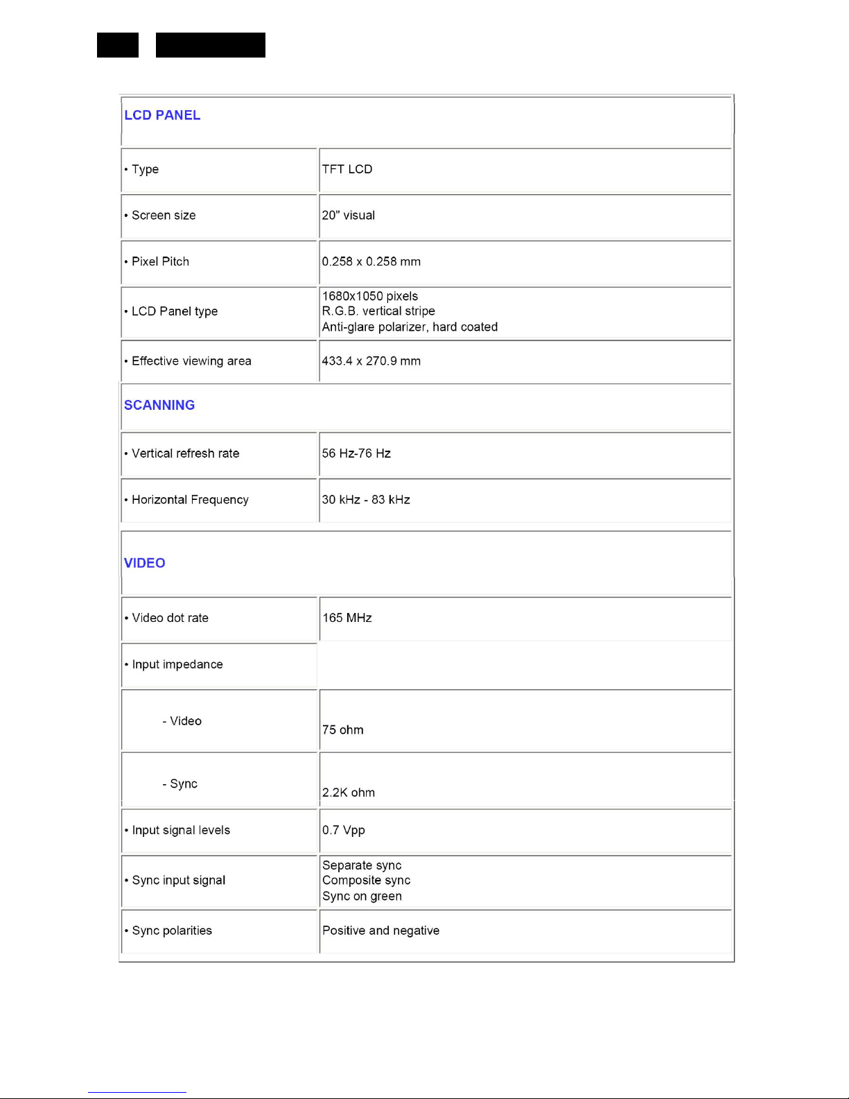
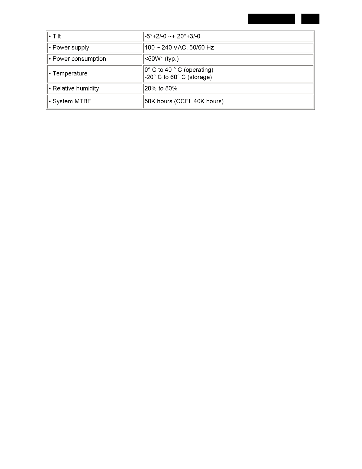
1. Monitor Specifications
HUDSON 8
5

HUDSON 8
6
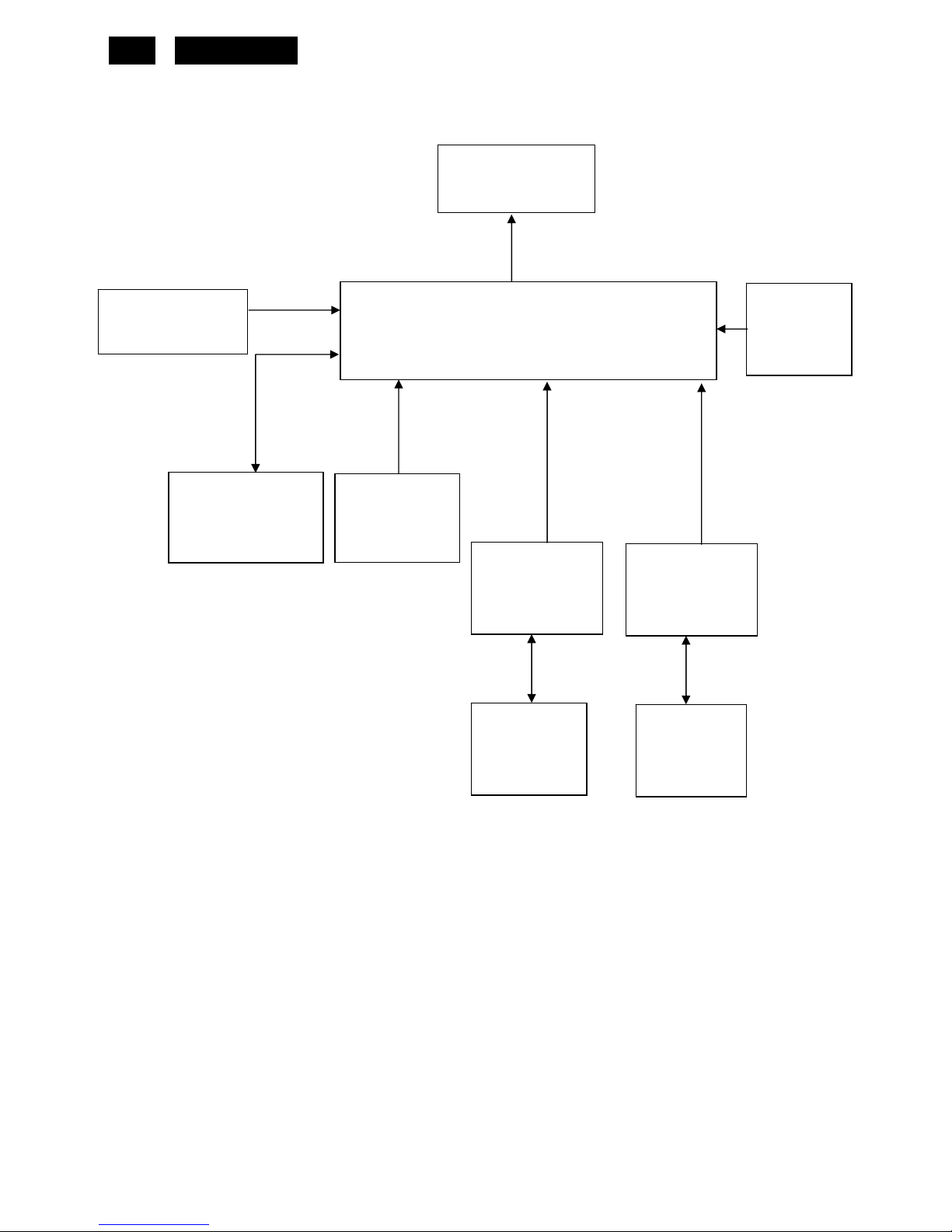
2. LCD Monitor Description
The LCD monitor will contain a main board, a power board and a key board which house the flat panel control logic,
brightness control logic and DDC.
The power board will provide AC to DC Inverter voltage to drive the backlight of panel and the main board chips
each voltage.
Monitor Block Diagram
AC-IN
100V-240V
Power board
(
Include: adapter, inverter)
Flat Panel and
CCFL backlight
Main Board
RS232 Connector
For white balance
adjustment in factory
mode
CCFL Drive.
Video signal, DDC
Key Board
HOST Computer
HUDSON 8
7
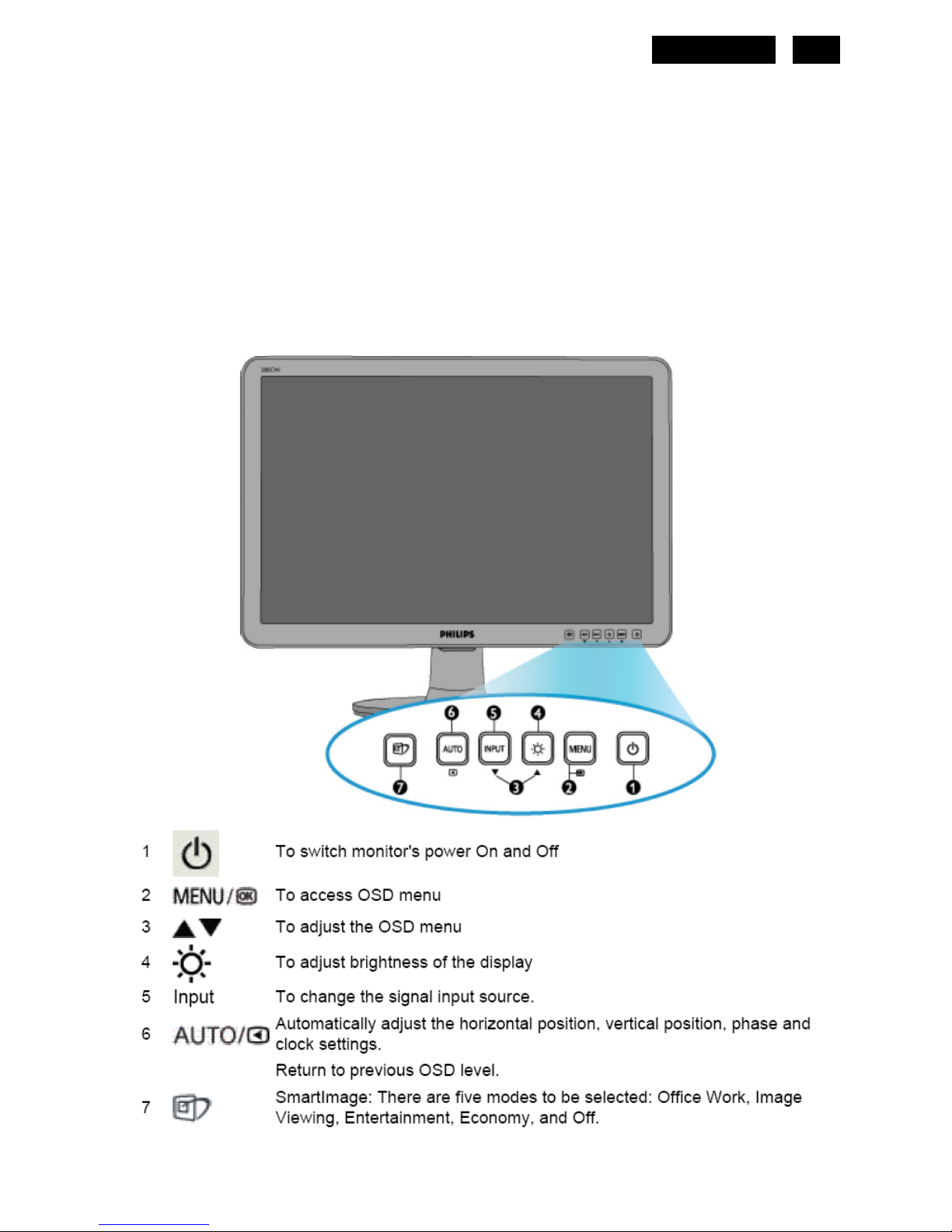
3. Operating Instructions
3.1 General Instructions
Press the power button to turn the monitor on or off. The other control buttons are located at the front of the
panel of the monitor.
By changing these settings, the picture can be adjusted to your personal preferences.
-
The power cord should be connected.
-
Connect the video cable from the monitor to the video card.
-
Press the power button to turn on the monitor, the power indicator will light up.
3.2 Control Buttons
Front View
HUDSON 8
8
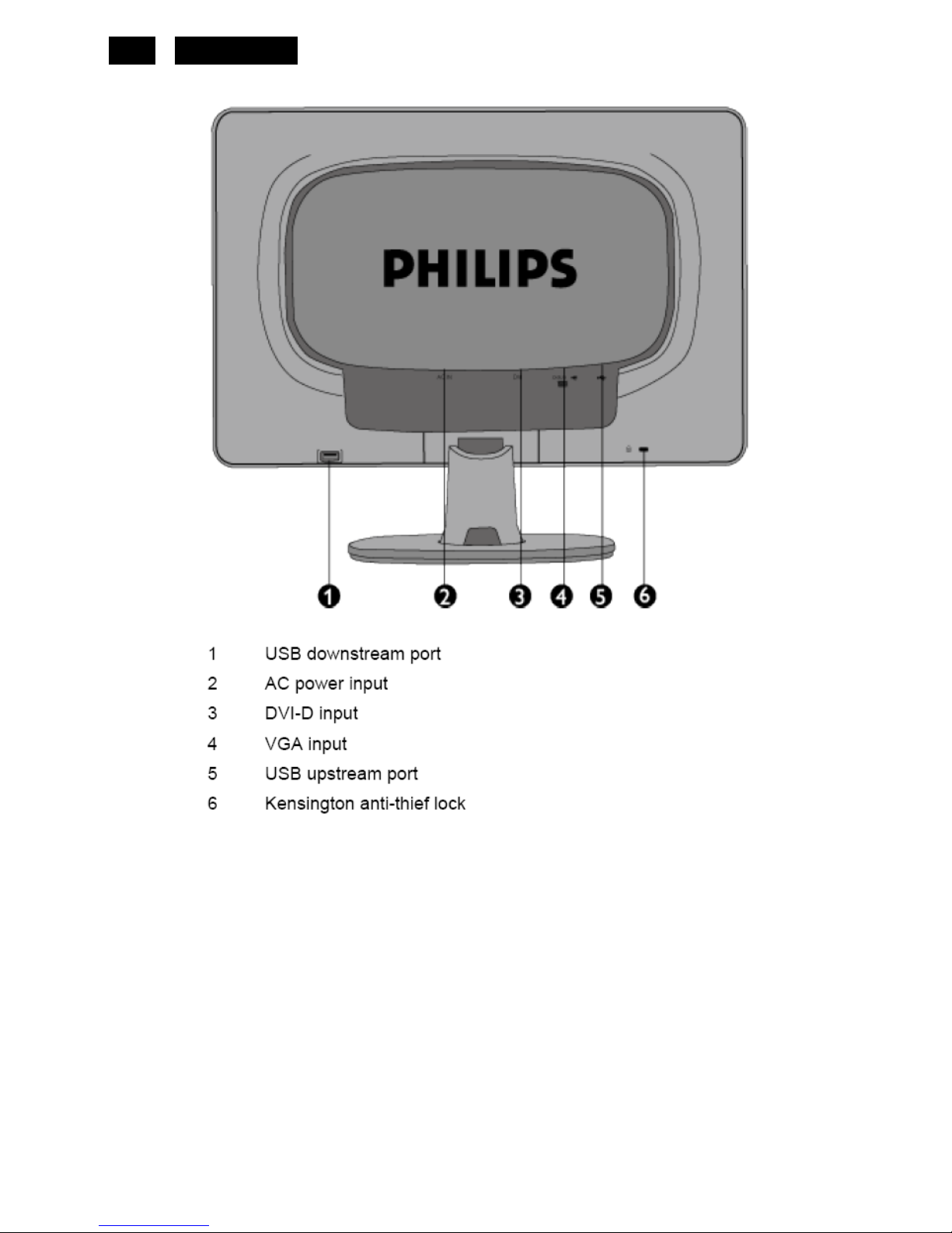
Rear View
HUDSON 8
9
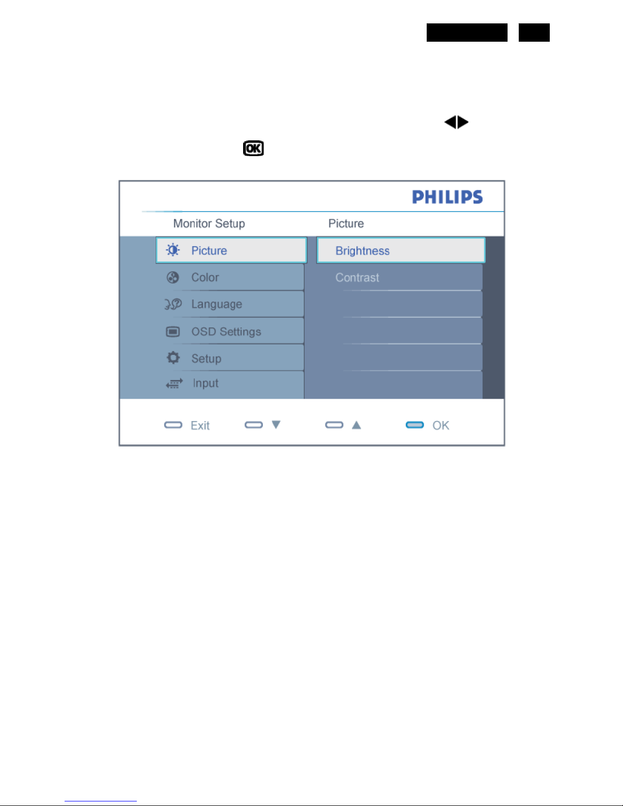
3.3 Adjusting the Picture
Description of the On Screen Display
On-Screen Display (OSD) is a feature in all Philips LCD monitors. It allows an end user to adjust screen
performance or select functions of the monitors directly through an on-screen instruction window. A user friendly on
screen display interface is shown as below. In the OSD shown above users can press
buttons at the front
bezel of the monitor to move the cursor,
to confirm the choice or change.
To Lock/Unlock OSD function (User Mode)
The OSD function can be locked by pressing “MENU” button for more than 10 seconds.
Locked OSD function can be released by pressing “MENU” button for more than 10 seconds again.
HUDSON 8
10
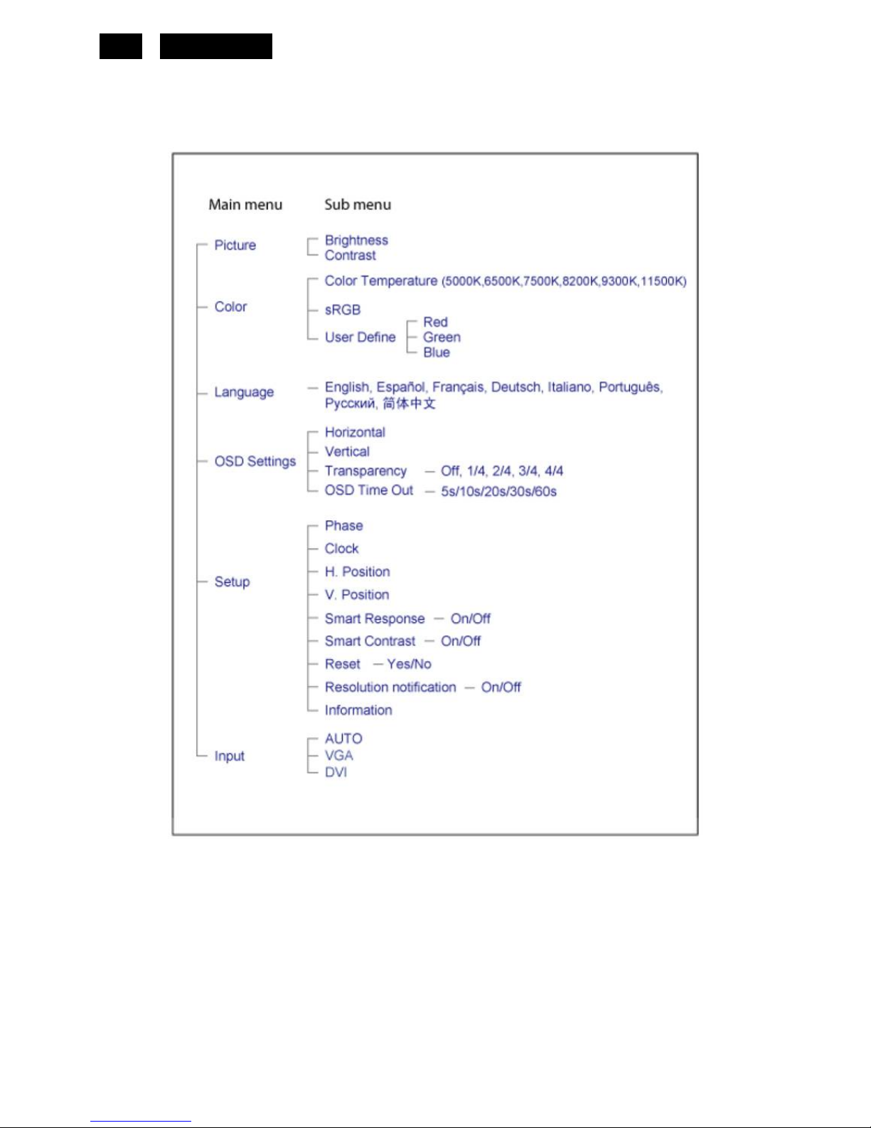
The OSD Tree
Below is an overall view of the structure of the On-Screen Display. You can use this as a reference when you want
to work your way around the different adjustments later on.
HUDSON 8
11
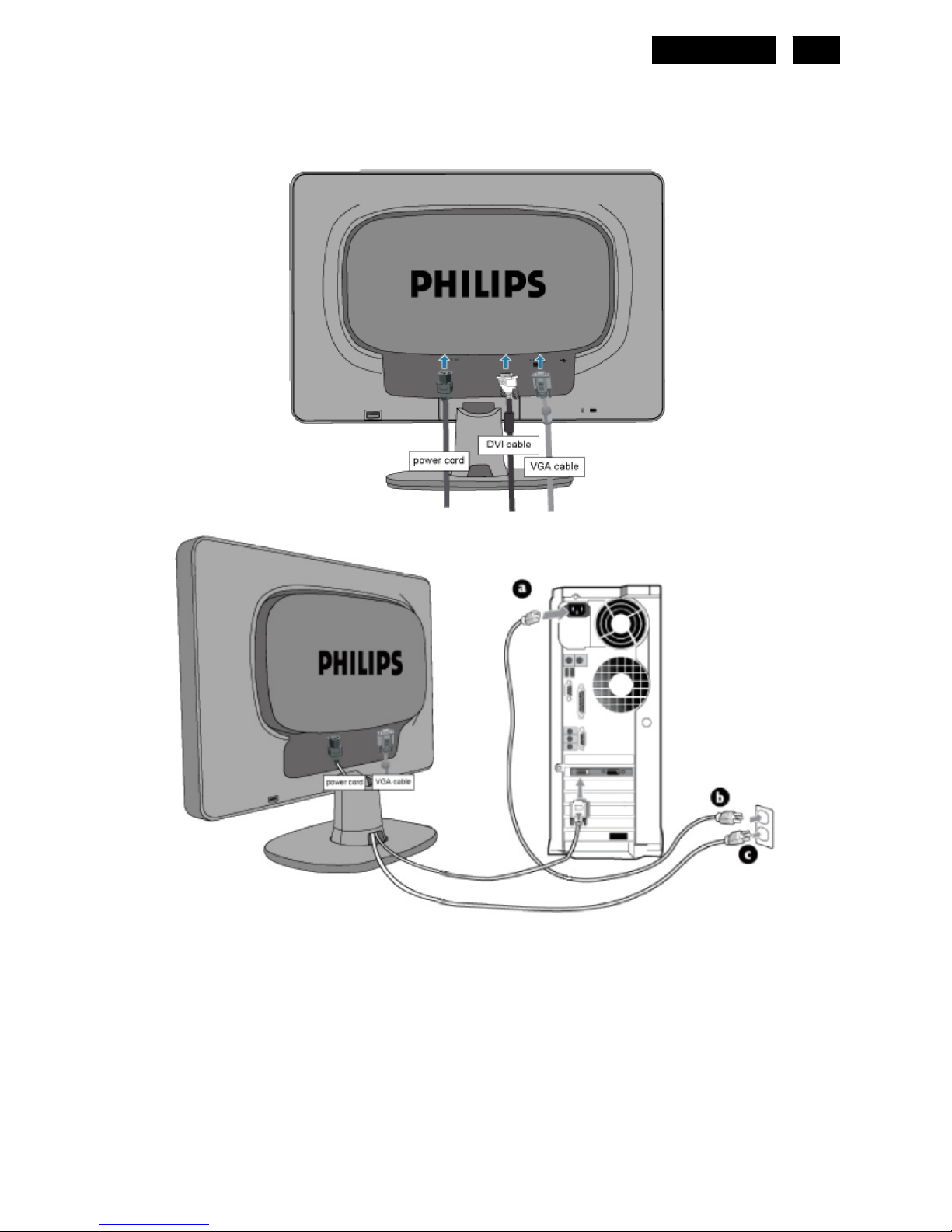
3.4 Connecting to the PC
1) Connect the power cord to the back of the monitor firmly. (Philips has pre-connected VGA cable for the first
installation.
2) Connect to PC
(a) Turn off your computer and unplug its power cable.
(b) Connect the monitor signal cable to the video connector on the back of your computer.
(c) Plug the power cord of your computer and your monitor into a nearby outlet.
(d) Turn on your computer and monitor. If the monitor displays an image, installation is complete.
HUDSON 8
12
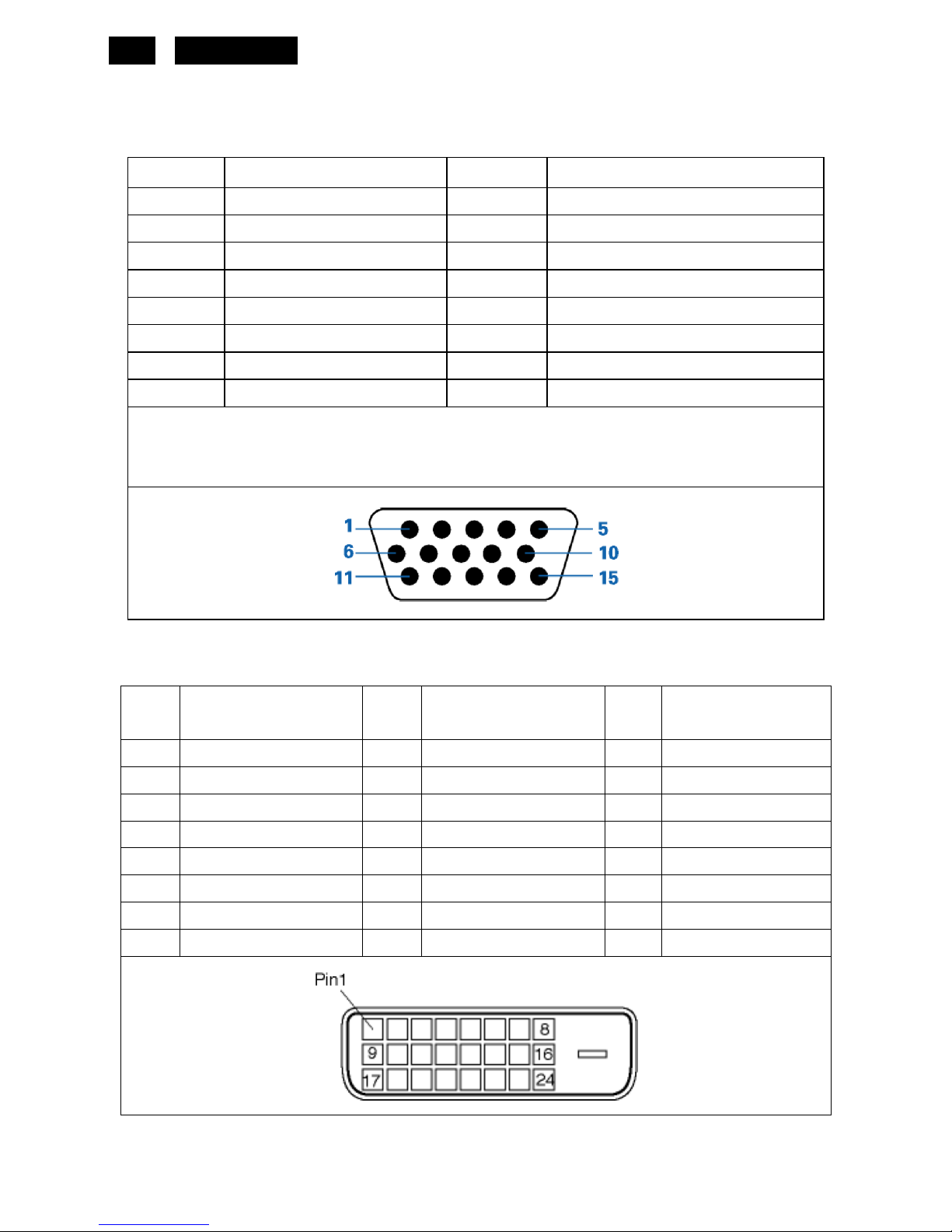
4. Input/ Output Specification
4.1 Input Signal Connector
Analog connectors
Pin No. Description Pin No. Description
1. Red video input 9. +5V
2. Green video input 10. Logic Ground
3. Blue video input 11. Ground
4. Sense (GND) 12. Serial data line (SDA)
5. Cable detect (GND) 13. H. Sync
6. Red video ground 14. V. Sync
7. Green video ground 15. Data clock line (SCL)
8. Blue video ground
VGA connector layout
DVI connectors
Pin
No.
Description
Pin
No.
Description
Pin
No.
Description
1. T.M.D.S Data2- 9. T.M.D.S Data1- 17. T.M.D.S Data0-
2. T.M.D.S Data2+ 10. T.M.D.S Data1+ 18. T.M.D.S Data0+
3. T.M.D.S Data2/4 Shield 11. T.M.D.S Data1/3 Shield 19. T.M.D.S Data0/5 Shield
4. No connector 12. No connector 20. No connector
5. No connector 13. No connector 21. No connector
6. DDC Clock 14. +5V Power 22. T.M.D.S Clock Shield
7. DDC Data 15. Ground (for +5V) 23. T.M.D.S Clock+
8. No connector 16. Hot Plug Detection 24. T.M.D.S Clock-
HUDSON 8
13
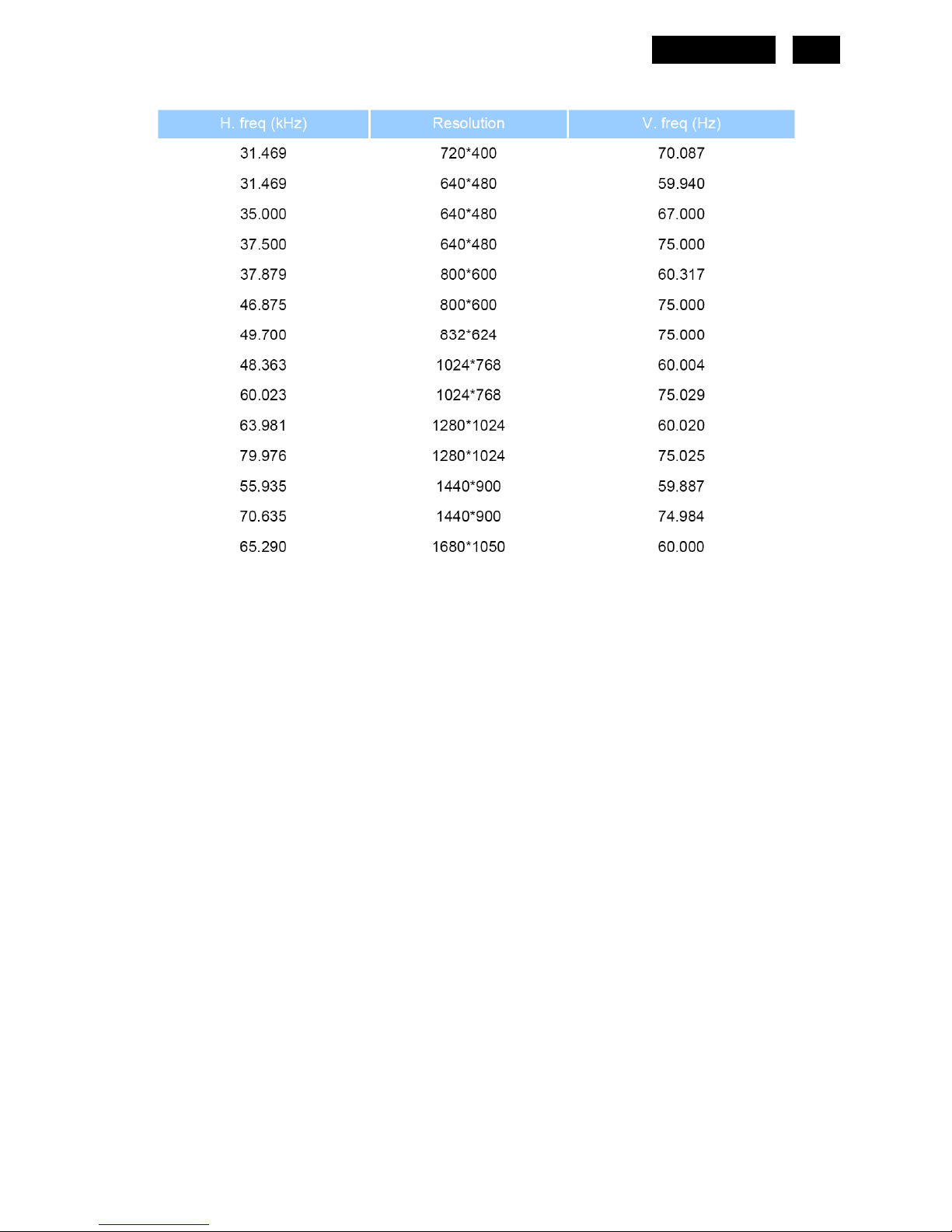
4.2 Factory Preset Display Modes
HUDSON 8
14
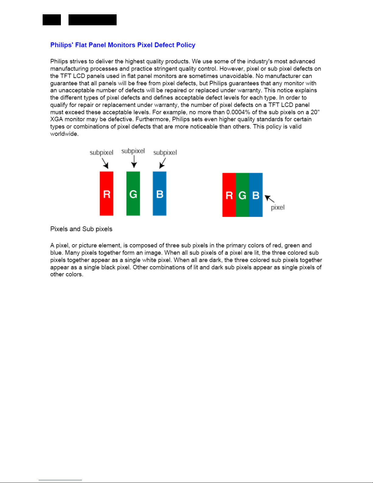
4.3 Pixel Defect Policy

HUDSON 8
15
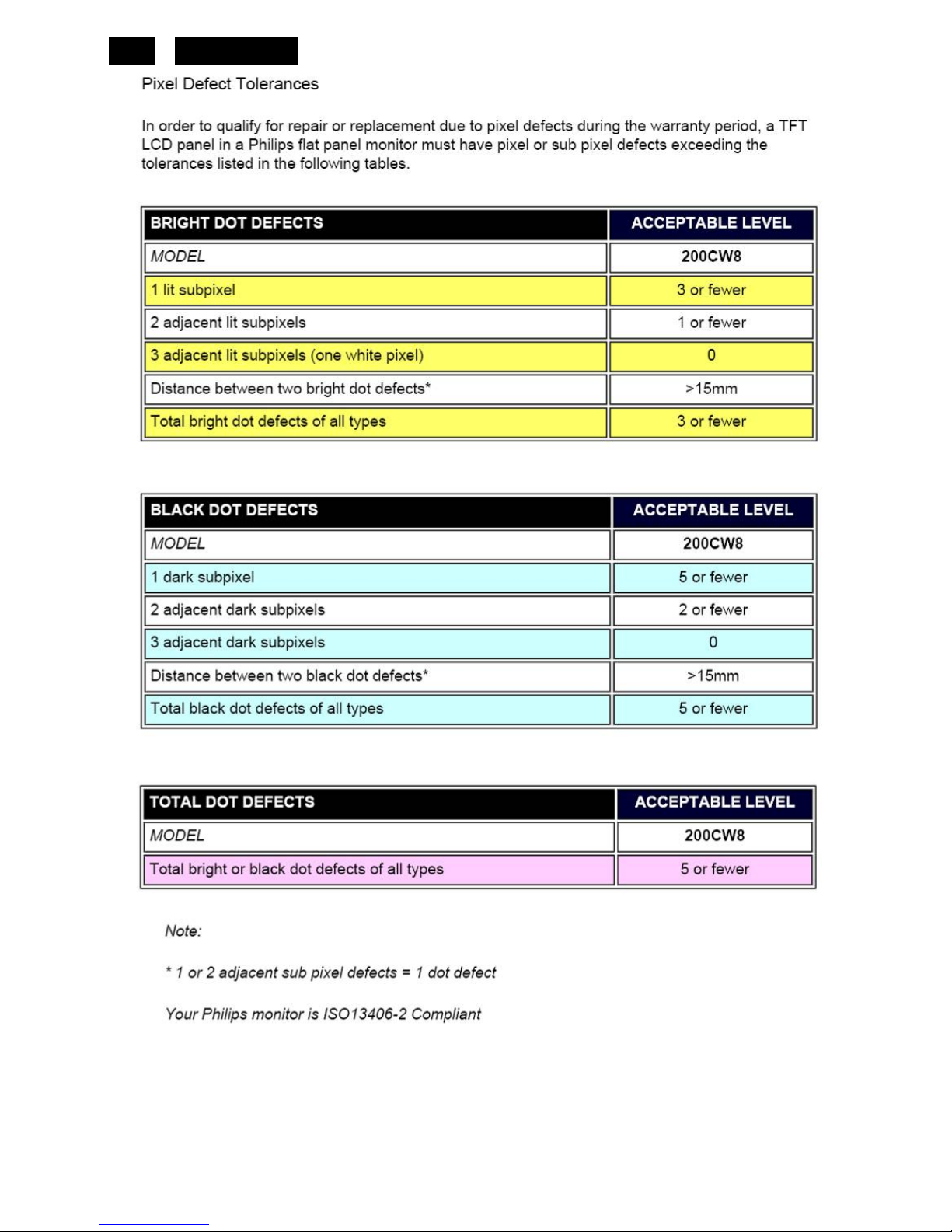
HUDSON 8
16

HUDSON 8
17
4.4 Failure Mode Of Panel
Failure description
Phenomenon
Vertical block defect
Vertical dim lines
Vertical lines defect
(Always bri
g
ht or dark)
Horizontal block de fect
Horizontal dim lines
Horizontal lines defect
(Always bri
g
ht or dark)
Has bri
g
ht or dark pixel
Polarizer has bubbles
Polarizer has bubbles
Foreign material inside
polarizer. It shows liner or
dot shape.
Concentric circle formed
Bottom back light of LCD is
brighter than normal
Back light un-uniformity
Backli
g
ht has foreign material.
Black or white color, liner or
circular type
Quick reference for failure mode of LCD panel
this pa
g
e presents problems that could be made by LCD panel.
It is not necessary to repair circuit board. Simply follow the mechanical
instruction on this manual to eliminate f ailure by replace LCD panel.
HUDSON 8
18
5. Block Diagram
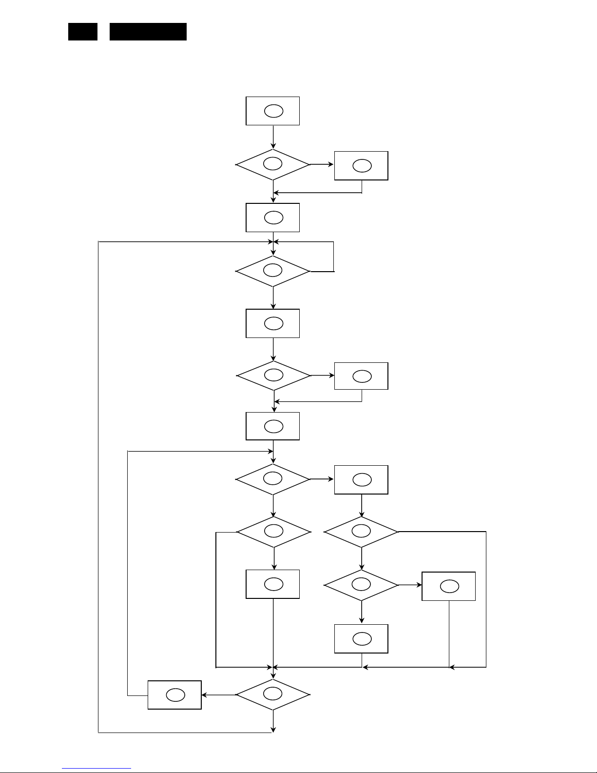
5.1 Software Flow Chat
1
2
N
Y
5
Y
N
10
Y
N
12
Y
N
7
Y
N
6
4
3
9
14
11
13
Y
N
15
Y
N
16
17
19
Y
N
18

HUDSON 8
19
1) MCU initialize.
2) Is the EPROM blank?
3) Program the EPROM by default values.
4) Get the PWM value of brightness from EPROM.
5) Is the power key pressed?
6) Clear all global flags.
7) Are the AUTO and SELECT keys pressed?
8) Enter factory mode.
9) Save the power key status into EPROM.
Turn on the LED and set it to green color.
Scalar initializes.
10) In standby mode?
11) Update the lifetime of back light.
12) Check the analog port, are there any signals coming?
13) Does the scalar send out an interrupt request?
14) Wake up the scalar.
15) Are there any signals coming from analog port?
16) Display "No connection Check Signal Cable" message. And go into standby mode after the message
disappear.
17) Program the scalar to be able to show the coming mode.
18) Process the OSD display.
19) Read the keyboard. Is the power key pressed?
HUDSON 8
20
5.2 Electrical Block Diagram
5.2.1 Main Board
Flash Memory
PM25LV010A-100SCE
(U402)
Panel Interface
(CN101)
Crystal
14.31818MHZ
(X401)
Keypad Interface
(CN401)
Scalar PUMO58CWHJ-LF
(Include MCU, ADC, OSD)
(U401)
D-Sub
Connector
(CN405)
EEPROM
AF24BC02-S1
(U404)
H sync
V sync
RGB
VGA_SDA,
VGA_SCL
DVI
Connector
(CN406)
EEPROM
AF24BC02-S1
(U405)
D-Data
D-Clock
DVI_SDA,
DVI
_
SCL
EEPROM
AF24BC16-SI
(U403)
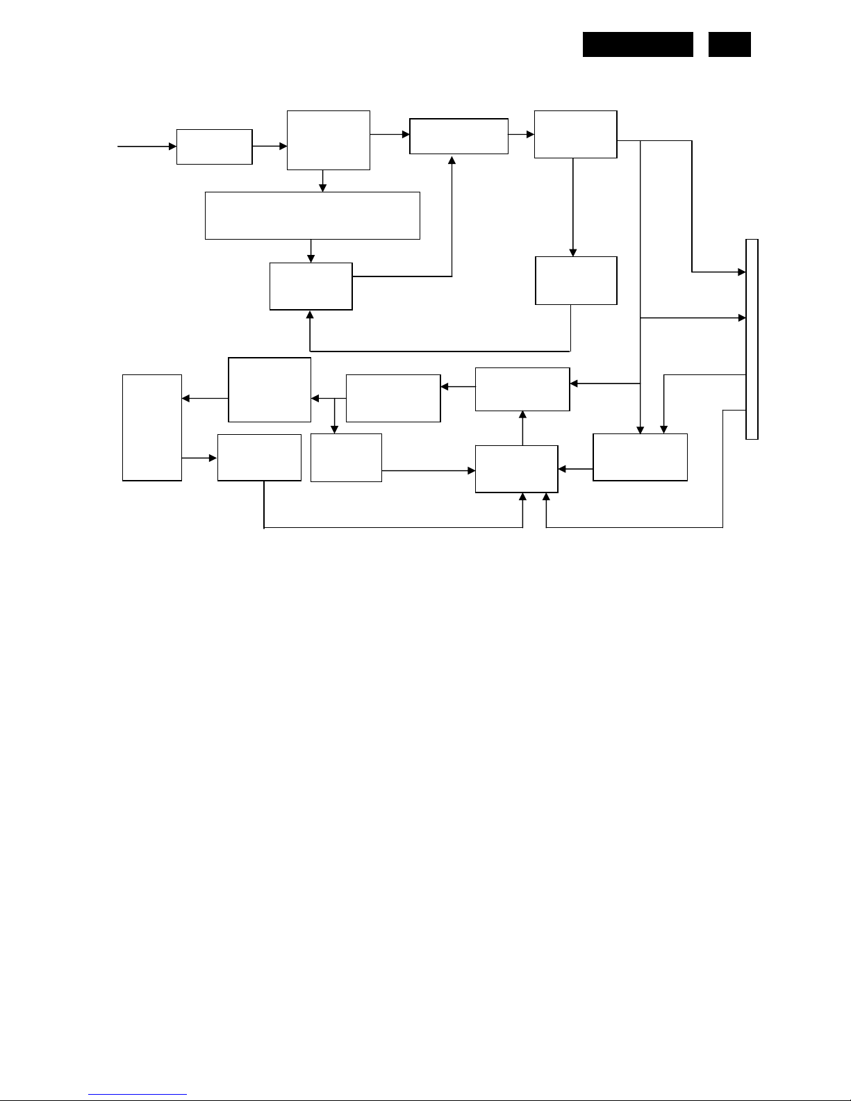
HUDSON 8
21
5.2.2 Inverter/Power Board
DIM
DIM
EMI filter
Start Circuit: R904、R905、R906
PWM
Control IC
Transformer
AC input
16V
ON/OFF
Control
PWM
Control IC
Feedback
Circui
t
Output
Circuit
Transformer
MOSFET
Over
Voltage
Lamp
ON/OFF
5V
Bridge
Rectifier
and Filter
Feedback
Circuit
Rectifier
diodes

HUDSON 8
22
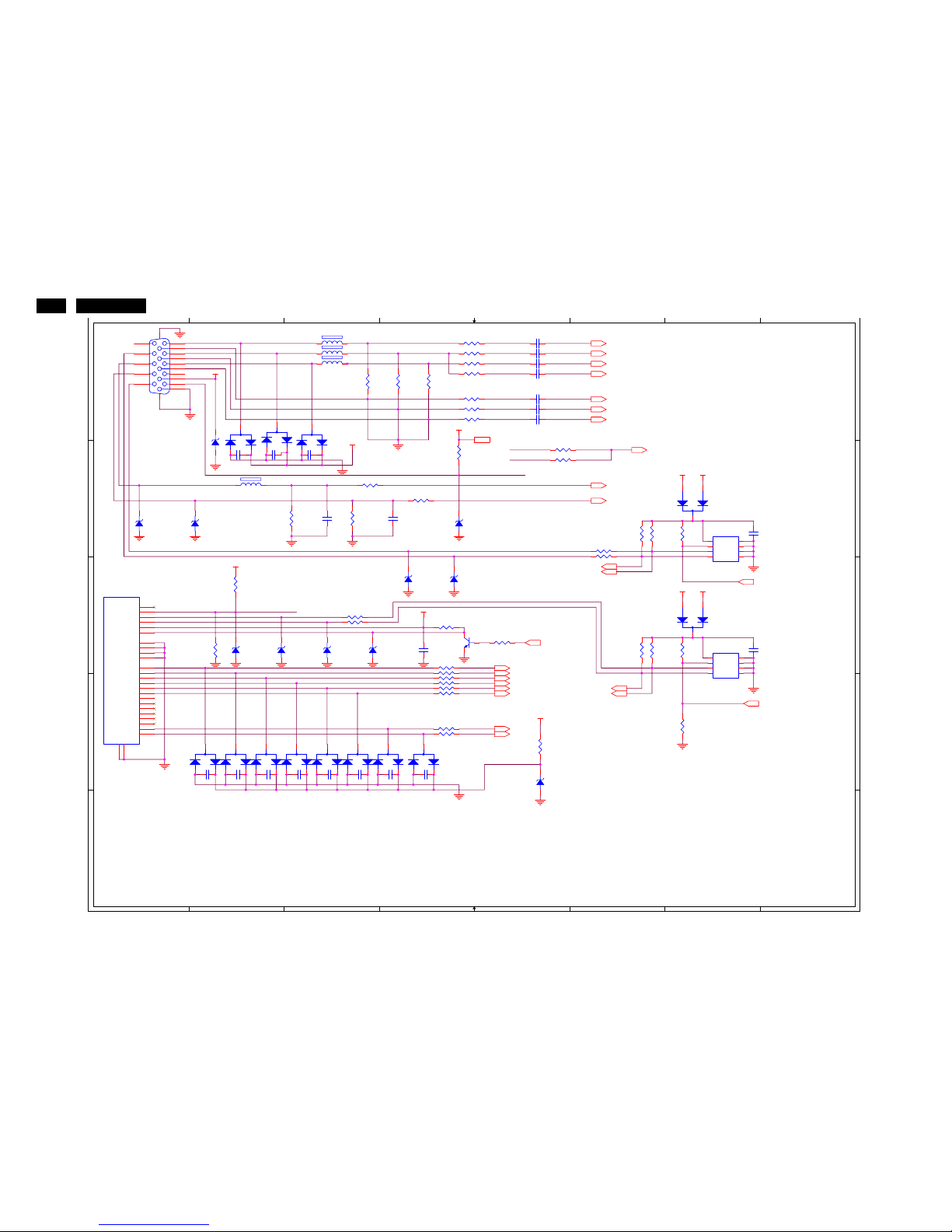
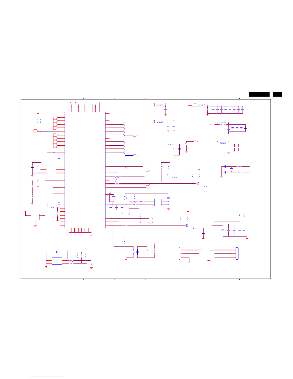
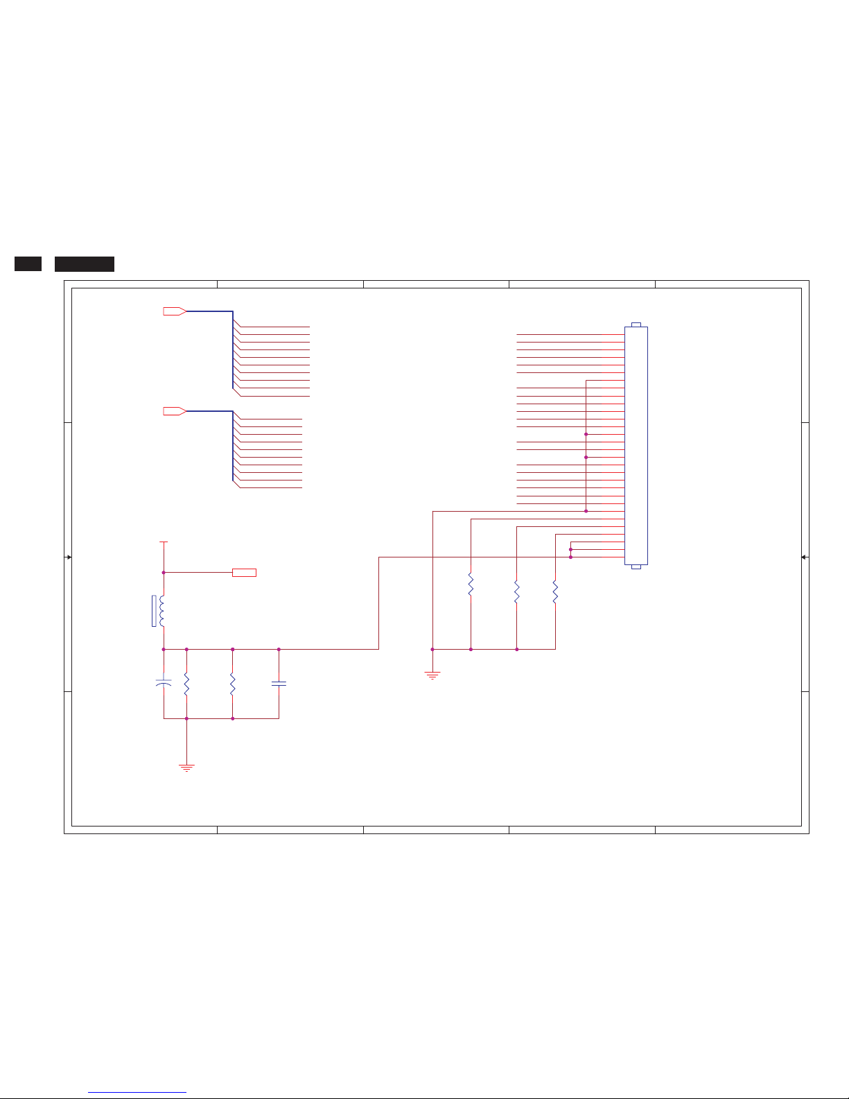
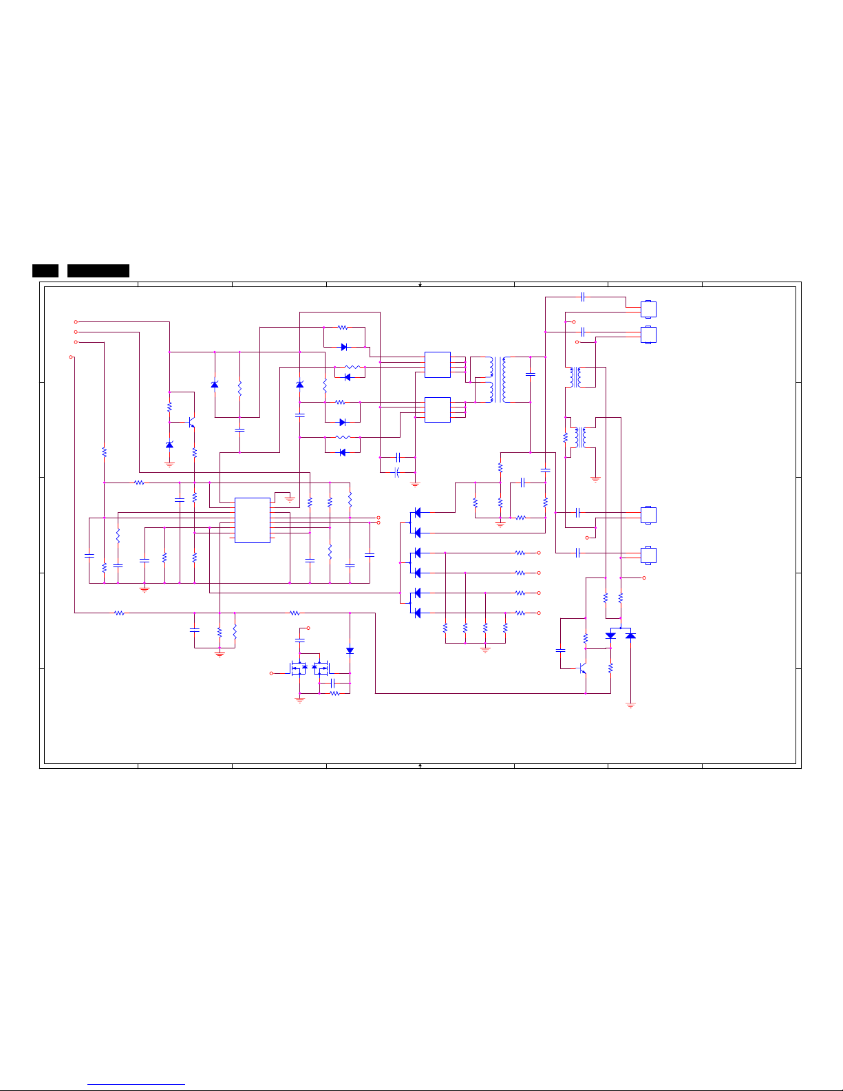
6. Schematic
6.1 Main Board
715G2592-1
1
1
2
2
3
3
4
4
5
5
6
6
7
7
8
8
A A
B B
C C
D D
E E
TSUMU58J SCHEMATIC
LVDS OUTPUT
TOP
B3
04.INPUT
RIN
GIN
BIN
VSYNC
GNDR
GNDG
GNDB
HSYNC
SOG
B+
CLK-
DET_INPUT
CLK+
R+
G+
R-
B-
G-
DDCA_SDA
DDCA_SCL
DDCD_SDA
DDCD_SCL
DDC_WP
+5V
HDCP_RST
B4
05.SCALER
RIN
GIN
SOG
BIN
GNDR
GNDG
GNDB
HSYNC
VSYNC
Adj_BACKLIGHT
VCC1.8
Vcc3.3
R+
R-
G-
G+
B+
BCLK+
CLK-
DDCD_SDA
DDCD_SCL
DET_INPUT
DDCA_SDA
DDCA_SCL
on_BACKLIGHT
on_Panel
+5V
DDC_WP
PA[0..9]
PB[0..9]
HDCP_RST
IDX
B2
03.POWER
on_Panel
on_BACKLIGHT
Adj_BACKLIGHT
VCC1.8
VLCD
+5V
VCC3.3 IDX
B5
06.PANEL INTERFACE
PB[0..9]
PA[0..9]
VLCD
PA[0..9]
PB[0..9]
VCC1.8
VCC3.3
VLCD
VCC1.8
VLCD
+5V
+5V
VCC3.3
+5V

HUDSON 8
23
1
1
2
2
3
3
4
4
5
5
6
6
7
7
8
8
A A
B B
C C
D D
E E
CN701 A1
CN702
C1
C702 D5
C708 A3
C709 A2
C710 A2
C711 B3
C712 C5
C713 C4
C714 C5
C715 E2
C717 E3
C718 E2
C719 E3
C724 D4
C725 D5
D704 C4
FB103 C2
FB406 A5
FB702 D3
FB703 E3
Q701 A4
Q703 B3
Q705 E2
Q706 E2
Q707 E3
R118 C1
R119 C2
R120 C2
R701 A4
R702 E1
R705 A4
R706 A4
R707 A4
R708 A3
R709 B3
R710 B3
R711 B4
R712 B3
R714 D2
R715 D2
R717 D1
R718 D4
R723 E2
R725 E1
R727 E3
R735 B2
R736 B3
U701 D5
U702 C5
U703 B5
U704 C5
POWER
ON/OFF
DIM
PANEL_ID
+5V
+5V
VLCD
VCC1.8
+5V
VCC3.3
+3V3
+3V3
+3V3
+3V3
+12V
+5V
VCC3.3
+12V
+12V
+12V
+5V
R725
4K7 1/16W
R718
3.3 OHM 3W
R710
NC/0R05 1/16W
C719
1uF/16V
FB702
120 OHM
1 2
R714
10K 1/16W
R727
10K 1/16W
U703
NC/LD1117S33
3 2
1
VI VO
GND
R736
NC/1K 1/16W
Q704
AM2321P
3
1
2
R712
4K7 1/16W
R702
NC/10K 1/16W
C711
0.1uF 16V
R717
10K 1/16W
C724
0.1uF 16V
U701
AP1117D18LA
123
ADJ(GND)
VOUT
VIN
Q706
NC/2N3904S-RTK/PS
R735
NC/4K7 1/16W
C714
0.1uF 16V
R723
10K 1/16W
D704
SSM24PT
R701
1K 1/16W
CN701
CONN
1
2
3
4
5
6
7
8
9
FB703
NC/120 OHM
12
C708
NC/1000pF
R119
NC/0R05 1/10W 5%
R706
NC/0R05 1/16W
C725
0.1uF 16V
R705
1K 1/16W
R120
NC/0R05 1/10W 5%
FB103
NC/120 OHM
1 2
+
C717
10uF/25V
U704
NC/AP1117E18LA
3 2
1
VI VO
GND
R711
10K 1/16W
FB406
600 OHM
C709
0.1uF 16V
+
C712
10uF/16V
CN702
NC/CONN
1
2
3
4
5
6
R709
15K 1/16W
C718
NC/1000pF
+
C710
100uF/25V
R707
4K7 1/16W
Q705
2N3906S-RTK/PS
R708
10K 1/16W
Q701
2N3904S-RTK/PS
C713
0.1uF 16V
R715
NC/10K 1/16W
+
C702
10uF/16V
C715
NC/1000pF
U702
AP1117D33LA
123
ADJ(GND)
VOUT
VIN
R118
NC/0R05 1/10W 5%
Q703
2N3904S-RTK/PS
Adj_BACKLIGHT 4
on_BACKLIGHT 4
+5V
VLCD 5
on_Panel4
VCC3.3 4
+5V3,4
VCC1.8 4
IDX 4
HUDSON 8
24
1
1
2
2
3
3
4
4
5
5
6
6
7
7
8
8
A A
B B
C C
D D
E E
CN405 A1 CN406 C1
C432 A5 C433 A5
C434 A5 C435 A5
C436 A5 C437 A5
C438 A5 C439 B2
C440 B2 C441 B3
C442 B3 C443 B4
C444 B7 C445 C4
C446 C7 C447 D2
C448 D2 C449 D2
C450 D3 C451 D3
C452 D3 C453 D4
C454 D4 D403 A2
D404 A2 D405 A3
D406 A2 D407 B7
D408 B1 D409 B2
D410 B4 D411 C4
D412 C4 D413 C7
D414 C2 D415 C3
D416 C3 D417 D2
D418 D2 D419 D2
D420 D2 D421 D3
D422 D3 D423 D3
D424 D4 D425 D5
D426 C2 FB409 B2
FB410 A3 FB411 A3
FB412 A3 Q406 C4
R401 C5 R434 A4
R435 A4 R436 A4
R437 A4 R438 A3
R439 A4 R440 A4
R441 A4 R442 A4
R443 A4 R444 B4
R445 B5 R446 B3
R447 B4 R448 B3
R449 B3 R450 B6
R451 B6 R452 B7
R453 B6 R454 B6
R455 C3 R456 C3
R457 C4 R458 B5
R459 C6 R460 C6
R461 C7 R462 C4
R463 C4 R464 C4
R465 C4 R466 D4
R467 D4 R468 D4
R469 D4 R470 D5
R471 C2 R472 C2
R473 D7 U404 B7
INPUT
ESD_5V
DET_VGA
DET_DVI
HSI
SDA_VGA
SCL_VGA
DET_VGA
PC5V
RED+
VGA_CON
GREEN+
RED-
GREENBLUE+
VSI
DAT1-
DAT2-
DCLK+
DAT0+
DAT0-
SCL_DVI
BLUE-
HPD
SDA_DVI
DAT1+
DCLK-
DET_DVI
DVI5V
DAT2+
ESD_5V
PC5V
+5V
+5V
+5V
+5V
+5V
DVI5V
DVI5V
PC5V
R466 10R 1/16W
D414
RLZ5.6B
R449
2K2 1/16W
C433 0.047uF
R440
75R 1/16W
R445 100R 1/16W
C437 0.047uF
D423
BAV99
3
1
2
D422
BAV99
3
1
2
R464 10R 1/16W
D415
RLZ5.6B
D425
RLZ5.6B
C442
22pF
R437 470R 1/16W
D421
BAV99
3
1
2
D420
BAV99
3
1
2
FB411 30 OHM
1 2
R436 56 OHM 1/16W
D419
BAV99
3
1
2
R451
4K7 1/16W 5%
D418
BAV99
3
1
2
D411
RLZ5.6B
R454 100R 1/16W
D417
BAV99
3
1
2
C448
0.1uF 16V
R458 100R 1/16W
R462 10R 1/16W
R472
NC/0R05 1/16W
D405
BAV99
3
1
2
D416
RLZ5.6B
R471
10K 1/16W
CN405
DB15
1
6
2
7
3
8
4
9
5
11
12
13
14
15
10
1716
D404
BAV99
3
1
2
R441 100R 1/16W
D403
BAV99
3
1
2
FB410 30 OHM
1 2
C443
220pF
C439
0.047uF
C454
0.1uF 16V
R470
1K 1/16W
R467 10R 1/16W
R469 10R 1/16W
R468 10R 1/16W
C435 1000pF
C444
0.22UF 10V
C452
0.1uF 16V
C432 0.047uF
D410
RLZ5.6B
C449
0.1uF 16V
FB412
30 OHM
1 2
R455 100R 1/16W
C445
0.1uF 16V
R457 10K 1/16W 5%
R439
75R 1/16W
C441
0.047uF
R435 56 OHM 1/16W
Q406
NC/2N3904S-RTK/PS
C450
0.1uF 16V
C434 0.047uF
R401
NC/4K7 1/16W
R450
4K7 1/16W 5%
R459
4K7 1/16W 5%
R456 100R 1/16W
R461
10K 1/16W
R453 100R 1/16W
C436 0.047uF
D408
RLZ5.6B
R465 10R 1/16W
U404
AF24BC02-SI
1
2
3
45
6
7
8
A0
A1
A2
VSSSDA
SCL
WP
VCC
R442 100R 1/16W
D413
BAV70
D412
RLZ5.6B
C453
0.1uF 16V
R463 10R 1/16W
C438 0.047uF
R434 56 OHM 1/16W
R443 100R 1/16W
C447
0.1uF 16V
D407
BAV70
CN406
JACK
1
2
3
4
5
6
7
8
9
10
11
12
13
14
15
16
17
18
19
20
21
22
23
24
26
25
DAT2-
DAT2+
2/4shield
DAT4-
DAT4+
DDC SCL
DDC SDA
VSYNC
DAT1-
DAT1+
1/3shield
DAT3-
DAT3+
+5V
SYNC GND
HPD
DAT0-
DAT0+
0/5shield
DAT5-
DAT5+
clk shield
clk+
clk-
GND
GND
R438
75R 1/16W
R446 1K 1/16W
R444
D409
RLZ5.6B
R460
4K7 1/16W 5%
D406
RLZ5.6B
R473
NC/0R05 1/16W
U405
AF24BC02-SI
1
2
3
45
6
7
8
A0
A1
A2
VSSSDA
SCL
WP
VCC
C446
0.22UF 10V
R447 1K 1/16W
D426
RLZ5.6B
FB409 120 OHM
R448
2K2 1/16W
C440
0.047uF
C451
0.1uF 16V
R452
10K 1/16W
D424
BAV99
3
1
2
RIN 4
GIN 4
BIN 4
VSYNC 4
GNDR 4
GNDG 4
GNDB 4
HSYNC 4
SOG 4
B+ 4
CLK- 4
CLK+ 4
R+ 4
G+ 4
R- 4
B- 4
G- 4
DDCA_SDA4
DDCA_SCL4
DDCD_SCL4
DDC_WP 4
DDC_WP 4
+5V 2,4
DDCD_SDA4
HDCP_RST 4
DET_INPUT4
HUDSON 8
25
1
1
2
2
3
3
4
4
5
5
6
6
7
7
8
8
A A
B B
C C
D D
E E
LVDS
Reset
Circuit
Unused Components
For HDCP
CN401 E5 CN407 E7
C401 B2 C402 A8
C403 A7 C404 A7
C405 A7 C406 A7
C407 B7 C408 A6
C409 A7 C410 A7
C411 A7 C412 A7
C413 A7 C414 B7
C415 B7 C416 A5
C417 B1 C418 C1
C419 A7 C420 A7
C421 B7 C422 B5
C423 B7 C424 D6
C425 C5 C426 D7
C427 D7 C428 D7
C429 D7 C430 D8
C455 A5 C456 C2
C457 C3 C458 C3
C459 C3 C460 C4
C461 A7 C464 A5
C470 E2 FB401 A7
FB402 B7 FB403 A6
FB404 A5 FB405 A5
OC1 E4 Q401 C5
Q402 B6 Q403 C6
Q409 D6 R403 B2
R404 C1 R405 B5
R406 B5 R407 C1
R408 C6 R409 C6
R411 C3 R413 B5
R414 B5 R415 D2
R418 C3 R419 C6
R420 C3 R421 C5
R422 C3 R423 C3
R424 C4 R425 C4
R426 C4 R427 C4
R428 C4 R429 C4
R474 D8 R475 D7
R476 E2 R477 E2
R478 E3 R479 E2
R480 E2 R481 E2
R482 E3 R486 B1
R487 C1 R488 B4
R489 A1 R490 A1
R491 D4 R492 D4
R493 D6 R494 D6
R495 D6 R496 D4
R497 E5 R499 D4
R501 B7 R502 B7
U401 A2 U402 B1
U403 C5 U406 D1
U408 E1 X401 B7
SCALER
LED_G
WP
XOUT
XIN
LED_A
POWER
KEY2
KEY1
LED_A
KEY1
KEY1
KEY2
LED_G
POWER
LED_A
LED_G
KEY2
POWER
KEY1
KEY2
POWER
LED_G
LED_A
LED_LF
HDCP_WP
WP
HDCP_WP
PA0
PA4
PB2
HDCP_SCL
PB9
IDX
PB6
HDCP_SDA
PB0
PB5
PA3
PA8
PB3
XIN
PA5
PA6
PB7
PB1
HDCP_SCL
XOUT
PB4
PA7
PA9
PA[0..9]
PB8
PA1
PB[0..9]
PA2
HDCP_SDA
LED_LF
LED_LF
AVDD_33
+5V
VCC3.3
VCC3.3
VCC1.8 VDDC
VCC3.3
+5V
VCC3.3
AVDD_18VCC1.8
AVDD_MEMPLL_33VCC3.3
+5V
VCC3.3
+5V
+5V
VCC3.3
VCC3.3
VCC3.3
VCC3.3
AVDD_33
VDDP
AVDD_33 VDDC
AVDD_18AVDD_MEMPLL_33
VCC3.3
VDDP
VDDP
VDDP
C421
22pF
R499
0R05 1/16W
R428 100R 1/16W
R420 100R 1/16W
C407
0.1uF 16V
R403
390 OHM 1/16W
R418 100R 1/16W
U402
PM25LV010A
1
2
3
4 5
6
7
8
CE#
SDO
WP#
VSS SDI
SCK
HOLD#
VDD
C426
1uF 10V
C424
1uF 10V
C459
0.1uF 16V
FB404
600 OHM
R404
10K 1/16W
FB403
600 OHM
C423
22pF
R493
10K 1/16W
+
C403
4.7uF/50V
R490NC/10K 1/16W
R406
10K 1/16W
C460
0.1uF 16V
R423 4K7 1/16W
C461
0.1uF 16V
C411
0.1uF 16V
R474
3.9K OHM 1/16W
R480 NC/100R 1/10W 5%
R477
NC/10K 1/10W 5%
+
C418
10uF/16V
C425
0.22uF
R422 4K7 1/16W
R411 100R 1/16W
C417
0.22uF
R486
3K3 1/16W
R491 4K7 1/16W
Q401
2N3906S-RTK/PS
Q409
2N3906S-RTK/PS
R481 NC/100R 1/10W 5%
R478
NC/10K 1/10W 5%
R429 100R 1/16W
FB405
600 OHM
U408
NC/CAT24WC08W
4
8
5
6
1
2
3
7
GND
VCC
SDA
SCL
A0
A1A2WP
C429
1uF 10V
R405
22K 1/16W
C416
0.1uF 16V
R487
10K 1/16W
R496
NC/10K 1/16W
CN401
CONN
1
2
3
4
5
6
7
C420
0.1uF 16V
R479 NC/100R 1/10W 5%
FB401
600 OHM
Q402
2N3904S-RTK/PS
R408
10K 1/16W
R427 100R 1/16W
C410
0.1uF 16V
R495
470R 1/16W 5%
R476
NC/10K 1/10W 5%
R501
20 OHM 1/16W
U403
M24C16
1
2
3
45
6
7
8
NC
NC
NC
VSSSDA
SCL
WC
VCC
C406
0.1uF 16V
C419
0.1uF 16V
R413
10K 1/16W
+
C464
22uF/16V
C413
0.1uF 16V
R421
0R05 1/16W
C409
0.1uF 16V
C428
1uF 10V
U406
NC/G690H438T73UF
1
23
GND
RSTVCC
R475
3.9K OHM 1/16W
C470 NC/0.22uF
C414
0.1uF 16V
C456
0.1uF 16V
R494
330R 1/16W 5%
C430
1uF 10V
OC1
NC/RBS310800
4 3
1 2
X401
14.3 Mhz
R407
NC/0R05 1/16W
R492
NC/10K 1/16W
R425
10K 1/16W
NC
NC
1
2
3
4
5
6
7
C402
0.1uF 16V
+
C408
10uF/16V
PUMO58CWHJ-LF
28
25
26
23
27
24
22
32
33
7
31
30
41
43
42
44
51
80
128
127
81
82
83
84
85
86
91
92
93
94
95
96
97
98
99
100
79
78
77
1
11
9
10
12
13
8
15
16
18
19
172952
104
87
37
103
112
34
35
5
6
118
14
107
36
73
119
120
121
123
124
117
116
115
38
39
108
3
4
53
74
40
59
7288101
76
75
102
109
126
114
111
110
20
90
89
122
2
113
56
55
57
61
64
70
67
21
106
105
48
49
47
45
46
50
686963
62
60
65
66
71
125
54
58
RIN0P
GIN0P
SOGIN0
BIN0P
RIN0M
GIN0M
BIN0M
HSYNC0
VSYNC0
REXT
REFP
REFM
SDO
SCK
CSZ
SDI
GPIO_P24/PWM2
LVACKM
XIN
XOUT
LVA2P
LVA2M
LVA1P
LVA1M
LVA0P
LVA0M
LVB3P
LVB3M
LVBCKP
LVBCKM
LVB2P
LVB2M
LVB1P
LVB1M
LVB0P
LVB0M
LVACKP
LVA3M
LVA3P
GND
GND
RX2P
RX2N
RX1P
RX1N
AVDD_33
RX0P
RX0N
RXCKP
RXCKN
GND
GND
GND
VDDC
VDDP
MODE
VCTRL
VDDP
DDCA_SDA/RS232_TX
DDCA_SCL/RS232_RX
DDCD_SDA
DDCD_SCL
NC
AVDD_33
VDDP
GPIO_P22/PWM1
GPIO_P04
GPIO_P00/SAR0
GPIO_P01/SAR1
GPIO_P02/SAR2
GPIO_P06
GPIO_P07
NC
NC
NC
I2C_MDA
I2C_MCL
RST
GPIO_P15
GPIO_P16
VDDC
VDDC
VDDP
VDDP
GND
GND
GND
NC
NC
BYPASS
GPIO_P25
VDDC
VDDP
NC
NC
AVDD_33
NC
NC
GPIO_P03/SAR3
GPIO_P14/PWM0
GND
NC
NC
NC
NC
NC
NC
NC
AVDD_18
GND
GND
GPIO_P44
GPIO_P43
GPIO_P45
GPIO_P47
GPIO_P46
GPIO_P42
GND
GND
GND
GND
VDDP
VDDP
VDDP
VDDP
GPIO_P13/PWM2
VDDP
AVDD_MEMPLL
C457
0.1uF 16V
FB402
600 OHM
R414
120R 1/16W
C415
0.1uF 16V
C412
0.1uF 16V
R409
120R 1/16W
R424
10K 1/16W
R489
NC/10K 1/16W
R488
100R 1/16W
R415
10K 1/16W
C404
0.1uF 16V
Q403
2N3906S-RTK/PS
R426
10K 1/16W
C405
0.1uF 16V
R502
20 OHM 1/16W
C422
0.1uF 16V
R497
NC/470R 1/16W
C455
0.1uF 16V
C401
0.1uF 16V
R482
NC/10K 1/10W 5%
C427
1uF 10V
C458
0.1uF 16V
R419 0R05 1/16W
VCC1.82
DDC_WP 3
VCC3.32
HDCP_RST 3
+5V 2
CLK+3
B+3
HSYNC3
adj_BACKLIGHT 2
GNDG3
PA[0..9] 5
RIN3
on_BACKLIGHT 2
PB[0..9] 5
R-3
DDCA_SDA3
G-3
VSYNC3
GNDR3
DDCD_SCL3
DDCA_SCL3
G+3
on_PANEL 2
B-3
BIN3
SOG3
IDX 2
DDCD_SDA3
CLK-3
R+3
GIN3
DET_INPUT3
GNDB3
1
1
2
2
3
3
4
4
5
5
A A
B B
C C
D D
CN101 A4
C720 C1
C721 C2
FB701 C1
R719 C2
R720 C1
R732 C4
R733 C3
R734 C3
Panel Interface
RXE3-LVA3M
RXE3+LVA3P
LVB2M RXO2-
RXOC+LVBCKP
LVBCKM RXOC-
LVACKM RXEC-
RXE2+LVA2P
RXE2-LVA2M
LVA0P RXE0+
RXO0-LVB0M
RXO2+LVB2P
RXE1+LVA1P
RXO0+LVB0P
RXO1+LVB1P
RXE0-LVA0M
RXO3+LVB3P
RXO1-LVB1M
RXO3-LVB3M
RXEC+LVACKP
RXE1-LVA1M
LVB3PPB0
LVB1PPB6
LVB2MPB5
LVB3MPB1
PA1 LVA3M
LVBCKMPB3
PA0 LVA3P
LVB1MPB7
PA5 LVA2M
PB[0..9]
PA7 LVA1M
LVB0MPB9
PA3 LVACKM
PA8 LVA0P
PA9 LVA0M
PA[0..9]
LVB2PPB4
PA6 LVA1P
PA2 LVACKP
LVB0PPB8
LVBCKPPB2
PA4 LVA2P
VLCD
+
C720
4.7uF/50V
FB701
120 OHM
1
2
R720
220 OHM 1/4W
R733
NC/0R05 1/16W
R734
NC/0R05 1/16W
CN101
CONN
1
2
3
4
5
6
7
8
9
10
11
12
13
14
15
16
17
18
19
20
21
22
23
24
25
26
27
28
29
30
R719
220 OHM 1/4W
R732
NC/0R05 1/16W
C721
0.1uF 16V
VLCD 2
PA[0..9]4
PB[0..9]4
26
26
HUDSON 8
HUDSON 8
27
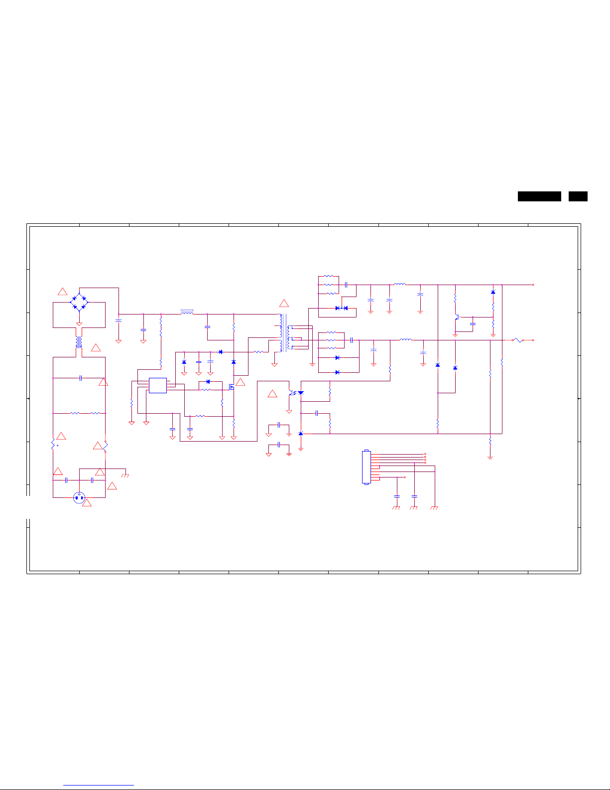
6.2 Power Board
715G2621-1
1
1
2
2
3
3
4
4
5
5
6
6
7
7
8
8
9
9
10
10
11
11
A A
B B
C C
D D
E E
F F
G G
H H
!
!
!
!
!
!
!
!
!
!
!
!
BD901 B1
CN901 G1
CN902 F7
C900 E5
C901 F2
C902 F1
C903 D1
C905 C2
C906 C4
C907 D4
C908 D4
C909 E4
C912 B7
C915 C8
C917 B7
C918 B8
C921 E5
C922 B8
C924 E6
C928 E3
C929 C7
C931 G8
C932 C9
C933 G8
C938 C3
C939 C7
D900 D4
D901 C4
D903 D4
D906 B7
D907 C7
D908 D7
FB902 B4
F901 E2
F903 C10
IC901 D3
IC903 D6
IC904 E6
L902 C1
L903 C8
L904 B8
NR901 E1
Q901 D4
Q903 C9
R901 E2
R902 E1
R903 C4
R904 C3
R905 C3
R906 D3
R909 C5
R910 D4
R912 E4
R914 E4
R915 D2
R918 B6
R919 B6
R920 B6
R924 D8
R925 D6
R926 E6
R927 D10
R930 E10
R935 C6
R938 D4
R939 C10
R940 D10
R942 E9
R943 B10
R946 B9
R961 C6
R962 C6
T901 C5
ZD902 B10
ZD906 D4
ZD921 D9
ZD922 D9
POWER
+16V
+5V
ON/OFF
DIM
PID
+5V
+16V
C931
0.1uF
C909
470pF/25V
C928
1000pF
R920100 1/4W
ǂ
T901
POWER X'FMR
4
95
6
3
1
11
7
12
10
8
R901
1M 1/4W
ǂ
R962 100 1/4W
ǂ
R924
150R 1/8W
C907
0.1uF
C932
0.001uF
R925
1K 1/8W
L902
27.0mH
1
4
2
3
D903
LL4148
CN902
CONN
1
2
3
4
5
6
7
8
9
10
R903
100KOHM +-5% 2WS
R914
0.43 OHM +-5% 2WS
C903
0.047UF
+
C915
470uF16V
ZD922
RLZ5.6B
1 2
C900
3300pF 250V
R915
100K OHM 1% 1/8W
C933
0.1uF
F901
FUSE
C912
0.001uF
ZD921
RLZ18B
1 2
R961 100 1/4W
ǂ
R909
5.1 1/4W
ǂ
R910
10 1/4W
ǂ
R930
2.43K 1% 1/10W
ǂ
Q903
PMBS3904
L903
3.5uH
D901
FR103
C906
1500pF2KV
D908
NC
CN901
SOCKET
12
3
C921
3300pF 250V
F903
䏇㎮
IC903
PC123X2YFZOF
12
43
R912
220 1/4W
ǂ
+
C922
NC
R902
1M 1/4W
ǂ
D900
BA159GPT
R939
1K 1/8W
ǂ
C924
0.1uF
ZD906
NC
1 2
C938
NC
R935 100 1/4W
ǂ
R918100 1/4W
ǂ
R942
1K 1/10W 1%
R926
1K 1/10W 1%
R905
300K 1/4W
ǂ
IC904
KIA431A-AT/P
R927
3.6K 1% 1/10W
ǂ
C901
1000PF/250VAC
+
C917
680uF25V
R904
300K 1/4W
ǂ
R940
43K OHM 1% 1/10W
+
C908
22uF/50V
R906
300K 1/4W
ǂ
D906
SP10150
123
R919100 1/4W
ǂ
ZD902
RLZ18B
1 2
C929
0.001uF
D907
31DQ06FC3
C902
1000PF/250VAC
+
C905
100uF/450V
IC901
LD7552BPS
1
2
3
4 5
6
7
8
GND
COMP
VCC
RT NC
CS
VCC
OUT
t
NR901
NTCR
12
L904
3.5uH
+
C918
680uF25V
+
C939
1000uF25V
-
+
BD901
KBP208G
2
1
3
4
R938
10K 1/8W
ǂ
Q901
STP10NK70ZFP
FB902
80OHM
1 2
R943
470 1/8W
ǂ
R946
150 2W
ǂ
HUDSON 8
28
1
1
2
2
3
3
4
4
5
5
6
6
7
7
8
8
1 1
2 2
3 3
4 4
5 5
CN801 A7 CN802 A7
CN803 C7 CN804 C7
C801 B3 C802 B3
C803 C1 C804 C1
C805 C2 C806 C2
C807 C3 C808 C3
C809 C4 C810 C4
C811 B4 C812 B4
C813 D2 C814 D3
C815 E4 C816 A6
C817 B6 C818 B6
C819 A6 C820 A6
C821 C6 C822 C6
C823 D6 D801 A4
D802 A4 D803 B4
D804 B4 D805 D4
D806 C4 D807 C4
D808 D4 D809 D6
IC801 C3 L801 A6
L802 B6 Q801 B2
Q802 D3 Q803 D3
Q804 D6 Q805 A5
Q806 B5 R801 B2
R802 B2 R803 A3
R804 A3 R805 A4
R806 A4 R807 B4
R808 B4 R813 B1
R814 B1 R815 C1
R816 C1 R817 C2
R818 C2 R819 C2
R820 C3 R821 C3
R822 C4 R823 D2
R824 D2 R825 D3
R826 E4 R827 B6
R828 B5 R829 C5
R830 C5 R836 C6
R837 C5 R838 C5
R839 C5 R840 D5
R841 D5 R842 D5
R843 D5 R844 D5
R845 D5 R846 D6
R847 D7 R848 D6
R849 D6 R850 D1
T801 A5 ZD801 B2
ZD802 A2 ZD803 A3
INVERTER
SST
LV1
ON/OFF
SST
DIM
CT
LV2
LV3
LV3
+16V
LV4
LV2
CT
LV1
LV4
PID
C817
2pF/3KV
Q803
2N7002
D806
BAV70
C814
390P 50V
+
C812
1000uF 25V
R839 1M 1/10W
ǂ
R816
10K 1/10W 1%
C823
NC
R820
10K 1/10W
ǂ
C809
560PF/50V
R848
NC
Q801
PMBS3904
ZD801
RLZ5.6B
1 2
R808
100R 1/8W
C822
68pF3KV
CN802
CONN
1
2
Q802
2N7002
C818
220pF
R830
NC
Q805
AM4502C-T1-PF
1
2
3
4
8
7
6
5
S
G
S
G
D
D
D
D
R804
5K1 1/8W
R842
10K 1/10W
ǂ
Q806
AM4502C-T1-PF
1
2
3
4
8
7
6
5
S
G
S
G
D
D
D
D
R840 1M 1/10W
ǂ
R815
NC
C807
0.01uF
R818
100K 1/10W
ǂ
D801
LL4148
R836
51K 1/10W
ǂ
C811
0.1uF
R841 1M 1/10W
ǂ
C802
0.047uF
C810
0.047uF
C819
68pF3KV
R837
8.2K 1/10W
ǂ
R819
100K 1/10W
ǂ
CN803
CONN
1
2
CN804
CONN
1
2
C816
12pF/6KV
R827
NC
C804
2.2uF/16V
R801
2.4K 1/10W
ǂ
R806
100R 1/8W
D804
LL4148
IC801
OZ9938GN
1
2
3
4
5
6
7
8 9
10
11
12
13
14
15
16
DRV1
VDDA
TIMER
DIM
ISEN
VSEN
OVPT
NC1 NC2
ENA
LCT
SSTCMP
CT
GNDA
DRV2
PGND
C805
0.01uF
R846
0 1/10W
ǂ
R817
1M 1/10W
ǂ
C808
180K 1/10W
R847
NC
R814
NC
C803
NC
R813
470K 1/10W
ǂ
R843
10K 1/10W
ǂ
R824
3K3 1/10W
D808
BAV70
R802
22 1/8W
ǂ
T801
POWER X'FMR
5
91
8
2
6
R850
100K 1/10W
ǂ
L801
L
124
3
R825
510 1/10W
ǂ
R826
1M 1/10W
ǂ
R807 100 1/10W
ǂ
C815
0.047uF
R828
6.2M 1/2W
ǂ
R849
0 1/10W
ǂ
R844
10K 1/10W
ǂ
C820
68pF3KV
Q804
NC
32
1
R821
1M 1/10W
ǂ
R803
5K1 1/8W
CN801
CONN
1
2
D807
BAV70
ZD803
RLZ5.6B
1 2
C801
0.047uF
R805
100 1/10W
ǂ
D803
LL4148
D805
LL4148
R823
390 1/10W
ǂ
R845
10K 1/10W
ǂ
C813
0.033uF
L802
L
124
3
D809
BAV99
3
1
2
C806
1uF/16V
R829
6.8K 1/8W
ǂ
R838 1M 1/10W
ǂ
D802
LL4148
ZD802
RLZ5.6B
1 2
C821
68pF3KV
R822
20K OHM 1% 1/8W
HUDSON 8
29
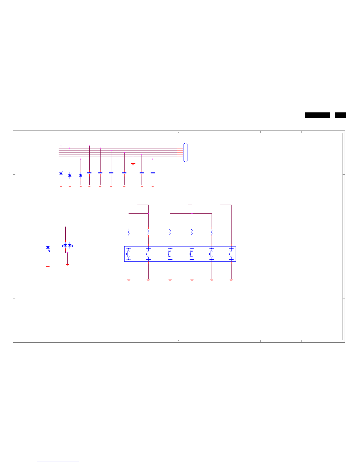
6.3 Key Board
715G2844-1
1
1
2
2
3
3
4
4
5
5
6
6
7
7
8
8
A A
B B
C C
D D
E E
KEY-DOWN KEY-POWERKEY-UP KEY-MENUKEY-AUTOKEY-LF
Pitch 1.0mm
CN001 A5
C001 A2
C002 A3
C003 A3
C004 A3
C005 A4
C006 A4
D001 A2
D002 A2
D003 A2
LED001
C2
LED002
C1
R001 C5
R002 C5
R003 C4
R007 C4
R008 C3
SW001
C3
LED_A
LED_G
KEY1 KEY2
LED_A
LED_G
POWER
POWER
KEY2
LED_LF
LED_LF
KEY1
C006
1uF 16V
C005
0.01uF/25V
R003
2.4K OHM 1% 1/10W
R007
4.3K OHM 1% 1/10W
C001
0.01uF/25V
SW001
1
2
3
4
5
6
7
8
9
10
11
12
C004
0.01uF/25V
R008
910 OHM 1% 1/10W
CN001
CONN
1
2
3
4
5
6
7
D003
UDZS5.6B
R002
910 OHM 1% 1/10W
C003
0.01uF/25V
R001
4.3K OHM 1% 1/10W
C002
0.01uF/25V
LED002
LED
12
D002
UDZS5.6B
LED001
LED
3
4
1
2
D001
UDZS5.6B
HUDSON 8
30
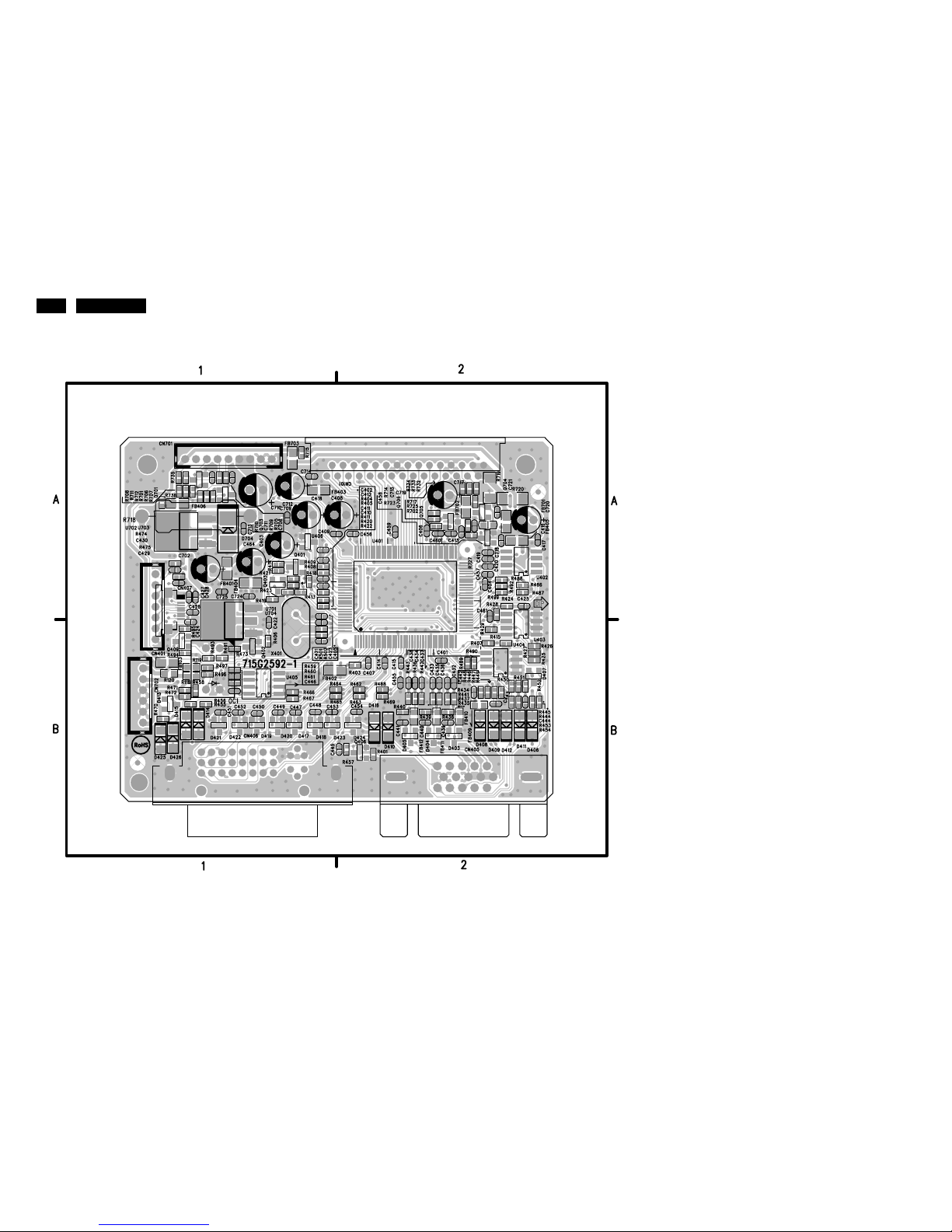
7. PCB Layout
7.1 Main Board
715G2592-1
C401 B2 C446 B1 D409 B2 R119 B1 R452 B2 R708 A1
C402 A1 C447 B1 D410 B2 R120 B1 R453 B2 R709 A1
C403 A1 C448 B1 D411 B2 R401 B2 R454 B2 R710 A1
C404 A2 C449 B1 D412 B2 R403 B2 R455 B1 R711 A1
C405 A1 C450 B1 D413 B1 R404 A1 R456 B1 R712 A1
C406 A2 C451 B1 D414 B1 R405 A1 R457 B2 R714 A2
C407 B2 C452 B1 D415 B1 R406 B1 R458 B1 R715 A1
C408 A2 C453 B1 D416 B2 R407 B2 R459 B1 R717 A2
C409 A1 C454 B2 D417 B1 R408 A1 R460 B1 R718 A1
C410 A1 C455 B2 D418 B1 R409 A1 R461 B1 R719 A2
C411 A1 C456 A2 D419 B1 R411 A1 R462 B2 R720 A2
C412 A1 C457 A2 D420 B1 R413 A1 R463 B2 R723 A2
C413 A2 C458 A2 D421 B1 R414 A1 R464 B1 R725 A2
C414 B2 C459 A2 D422 B1 R415 B2 R465 B1 R727 A2
C415 B2 C460 A2 D423 B2 R418 A1 R466 B1 R732 A2
C416 A2 C461 A2 D424 B2 R419 A1 R467 B1 R733 A2
C417 A2 C464 A1 D425 B1 R420 A1 R468 B2 R734 A2
C418 A1 C702 A1 D426 B1 R421 A1 R469 B2 R735 A1
C419 A2 C708 A1 D704 A1 R422 A1 R470 B1 R736 A1
C420 A2 C709 A1 FB103 B1 R423 A1 R471 B1
C421 B1 C710 A1 FB401 A1 R424 A2 R472 B1
C422 B1 C711 A1 FB402 B1 R425 B2 R473 B1
C423 B1 C712 A1 FB403 A1 R426 B2 R474 A1
C424 B1 C713 A1 FB404 A1 R427 B2 R475 A1
C425 A2 C714 A1 FB405 A2 R428 A2 R486 A2
C426 A1 C715 A2 FB406 A1 R429 B2 R487 A2
C427 A1 C717 A2 FB409 B2 R434 B2 R488 A2
C428 A1 C718 A2 FB410 B2 R435 B2 R489 B2
C429 A1 C719 A2 FB411 B2 R436 B2 R490 B2 U401 A2
C430 A1 C720 A2 FB412 B2 R437 B2 R491 B1 U402 A2
C432 B2 C721 A2 FB701 A2 R438 B2 R492 A2 U403 B2
C433 B2 C724 A1 FB702 A2 R439 B2 R493 B1 U404 B2
C434 B2 C725 A1 FB703 A1 R440 B2 R494 B1 U405 B1
C435 B2 CN101 A2 Q401 A1 R441 B2 R495 B1 U406 A1
C436 B2 CN401 A1 Q402 B1 R442 B2 R496 B1 U701 B1
C437 B2 CN407 A1 Q403 A1 R443 B2 R497 B1 U702 A1
C438 B2 CN701 A1 Q406 B2 R444 B2 R499 A2 U703 A1
C439 B2 CN702 B1 Q409 B1 R445 B2 R501 B1 U704 B1
C440 B2 D403 B2 Q701 A1 R446 B2 R502 B1 X401 A1
C441 B2 D404 B2 Q703 A1 R447 B2 R701 A1
C442 B2 D405 B2 Q704 A2 R448 B2 R702 A2
C443 B2 D406 B2 Q705 A2 R449 B2 R705 A1
C444 B2 D407 B2 Q706 A2 R450 B2 R706 A1
C445 B2 D408 B2 R118 B1 R451 B2 R707 A1
 Loading...