

Philips 1PS89SS06, 1PS89SS05, 1PS89SS04 Datasheet

DISCRETE SEMICONDUCTORS
DATA SH EET
M3D425
1PS89SS04; 1PS89SS05;
1PS89SS06
High-speed double diodes
Preliminary specification
Supersedes data of 1999 Mar 01
1999 Jun 08
Philips Semiconductors Preliminary specification
High-speed double diodes
FEATURES
• Power dissipation comparable to
SOT23
• Ultra small plastic SMD package
• High switching speed: max. 4 ns
• Continuous reverse voltage:
max. 80 V
• Repetitive peak reverse voltage:
max. 85 V
• Repetitive peak forward current:
max. 500 mA.
APPLICATIONS
• High speed switching in e.g.
surface mounted circuits.
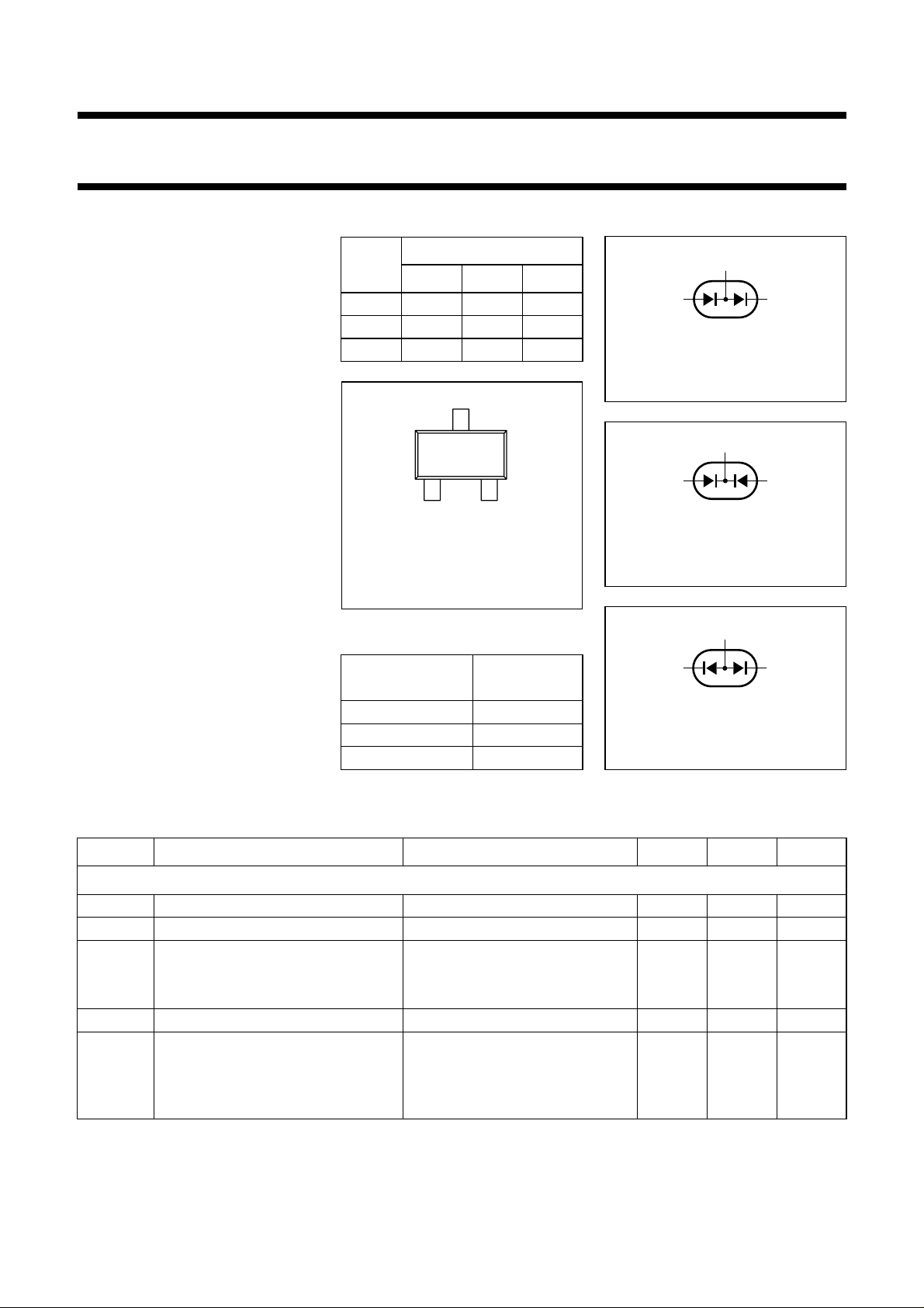
DESCRIPTION
Two high-speed switching diodes in
planar technology, with different
configurations, in an ultra small
SC-89 (SOT490) plastic SMD
package.
PINNING
1PS89SS..
PIN
04 05 06
1a
2k
1
2
3k1,a2k1,k
page
12
Top view
Fig.1 Simplified outline
(SC-89; SOT490) and
pin configuration.
MARKING
TYPE NUMBER
1PS89SS04 S4
1PS89SS05 S5
1PS89SS06 S6
a
1
a
2
2
3
MBK837
MARKING
CODE
1PS89SS04; 1PS89SS05;
1PS89SS06
3
k
1
k
2
a1,a
2
Fig.2 1PS89SS04 diode
Fig.3 1PS89SS05 diode
Fig.4 1PS89SS06 diode
12
MGL550
configuration (symbol).
3
12
MGL551
configuration (symbol).
3
1
MGL552
configuration (symbol).
2
LIMITING VALUES
In accordance with the Absolute Maximum Rating System (IEC 134).
SYMBOL PARAMETER CONDITIONS MIN. MAX. UNIT
Per diode unless otherwise specified
V
V
I
RRM
R
F
repetitive peak reverse voltage − 85 V
continuous reverse voltage − 80 V
continuous forward current T
=25°C; note 1; see Fig.5
amb
single diode loaded − 200 mA
both diodes loaded − 125 mA
I
FRM
I
FSM
repetitive peak forward current − 500 mA
non-repetitive peak forward current square wave; Tj=25°C prior to
surge; see Fig.7
t=1µs − 4A
t=1s − 0.5 A
1999 Jun 08 2

Philips Semiconductors Preliminary specification
High-speed double diodes
1PS89SS04; 1PS89SS05;
1PS89SS06
SYMBOL PARAMETER CONDITIONS MIN. MAX. UNIT
P
tot
T
stg
T
j
Note
1. Refer to SC-89 (SOT490) standard mounting conditions.
ELECTRICAL CHARACTERISTICS
=25°C unless otherwise specified.
T
j
SYMBOL PARAMETER CONDITIONS TYP. MAX. UNIT
Per diode
V
F
I
R
C
d
t
rr
V
fr
total power dissipation (per package) T
≤ 25 °C; note 1 − 250 mW
amb
storage temperature −65 +150 °C
junction temperature − +150 °C
forward voltage see Fig.6
I
= 1 mA 610 − mV
F
= 10 mA 740 − mV
I
F
I
=50mA − 1V
F
I
= 100 mA − 1.2 V
F
reverse current see Fig.8
V
=25V − 30 nA
R
=80V − 0.5 µA
V
R
V
= 25 V; Tj= 150 °C − 30 µA
R
V
= 80 V; Tj= 150 °C − 100 µA
R
diode capacitance f = 1 MHz; VR= 0; see Fig.9
1PS89SS04 − 1.5 pF
1PS89SS05 − 1.5 pF
1PS89SS06 − 2pF
reverse recovery time switched from IF= 10 mA to IR=10mA;
− 4ns
RL= 100 Ω; measured at IR= 1 mA;
see Fig.10
forward recovery voltage switched to IF= 10 mA; tr=20ns;
− 1.75 V
see Fig.11
THERMAL CHARACTERISTICS
SYMBOL PARAMETER CONDITIONS VALUE UNIT
R
th j-s
thermal resistance from junction to soldering point both diodes loaded
1PS89SS04 55 K/W
1PS89SS05 70 K/W
1PS89SS06 70 K/W
R
th j-a
thermal resistance from junction to ambient note 1 500 K/W
Note
1. Refer to SC-89 (SOT490) standard mounting conditions.
1999 Jun 08 3
Philips Semiconductors Preliminary specification
High-speed double diodes
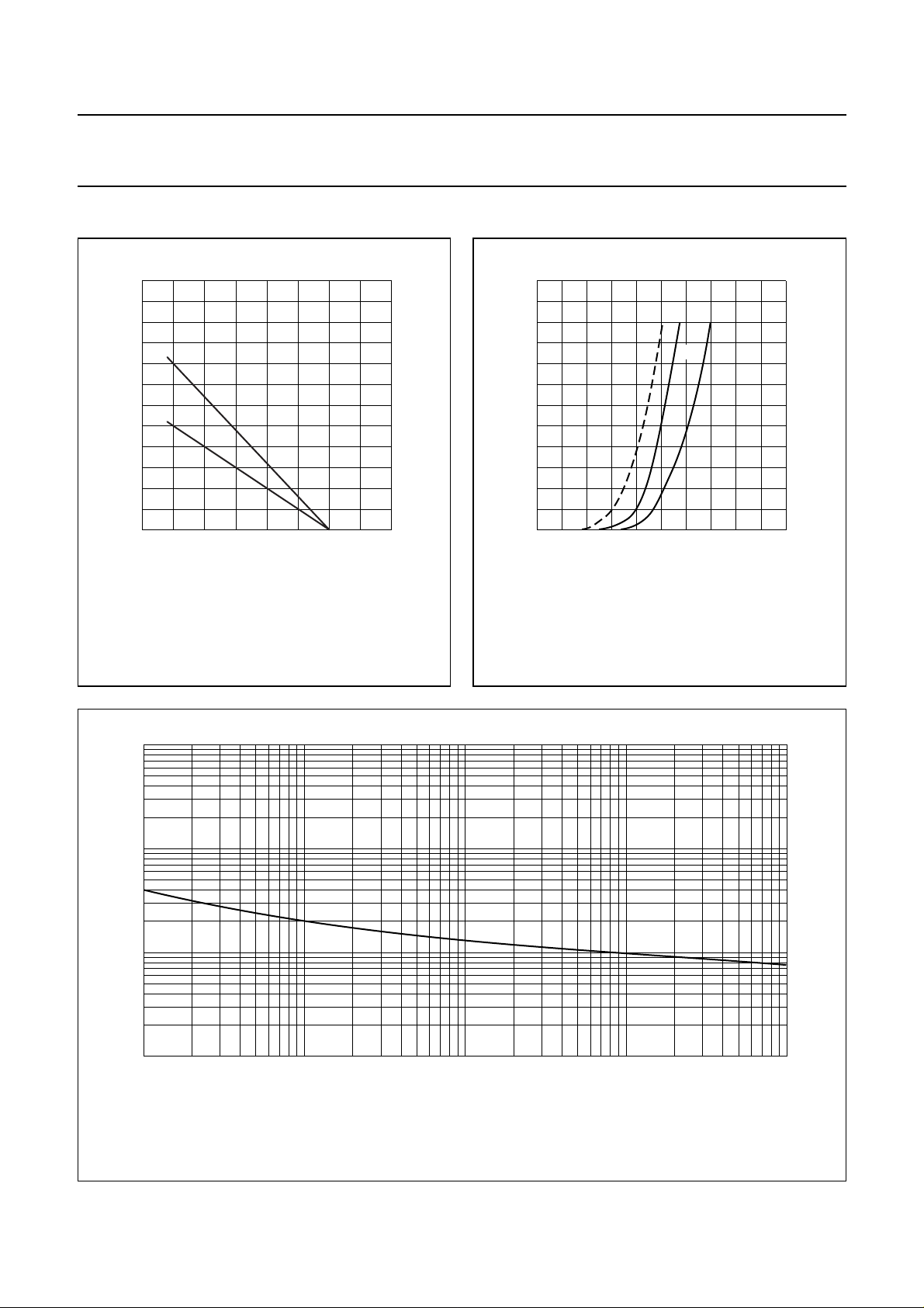
GRAPHICAL DATA
150
T
amb
MGL553
(°C)
300
handbook, halfpage
I
F
(mA)
(1)
200
(2)
100
0
050
(1) One diode loaded.
(2) Both diodes loaded.
100 200
Fig.5 Maximum permissible continuous forward
current as a function of the ambient
temperature.
1PS89SS04; 1PS89SS05;
1PS89SS06
300
handbook, halfpage
I
F
(mA)
200
100
0
02
(1) Tj= 150°C; typical values.
(2) Tj=25°C; typical values.
(3) Tj=25°C; maximum values.
(1) (3)(2)
1
Fig.6 Forward current as a function of forward
voltage.
MBG382
VF (V)
2
10
handbook, full pagewidth
I
FSM
(A)
10
1
−1
10
1
Based on square wave currents.
Tj=25°C prior to surge.
Fig.7 Maximum permissible non-repetitive peak forward current as a function of pulse duration.
MBG704
10
2
10
3
10
tp (µs)
4
10
1999 Jun 08 4
 Loading...