Philips 1PS79SB30 Datasheet

DISCRETE SEMICONDUCTORS
DATA SH EET
M3D319
1PS79SB30
Schottky barrier diode
Product specification 2001 Feb 20

Philips Semiconductors Product specification
Schottky barrier diode 1PS79SB30
FEATURES
PINNING
• Very low forward voltage
• Very low reverse current
• Guard ring protected
• Ultra small SMD package.
APPLICATIONS
• Ultra high-speed switching
• Voltage clamping
handbook, halfpage
• Protection circuits
• Blocking diodes
• Low power consumption applications (e.g. hand-held
applications).
Marking code: G1.
DESCRIPTION
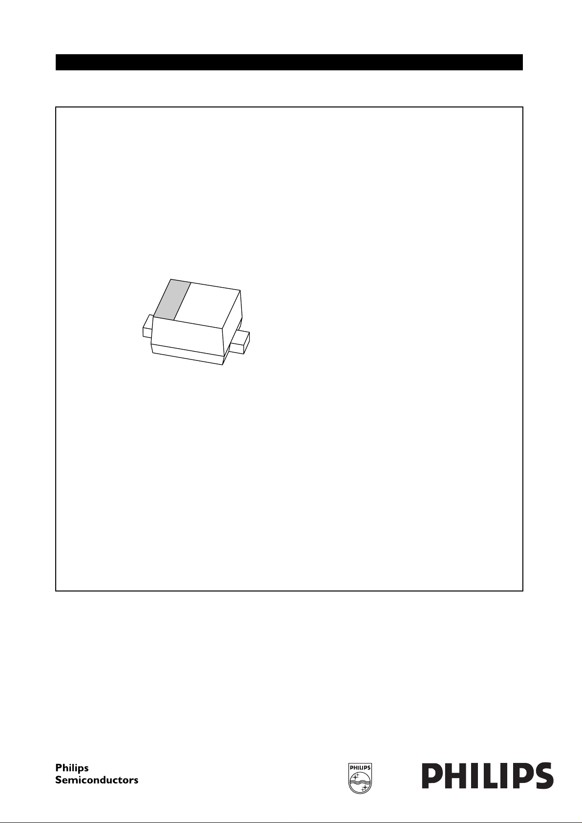
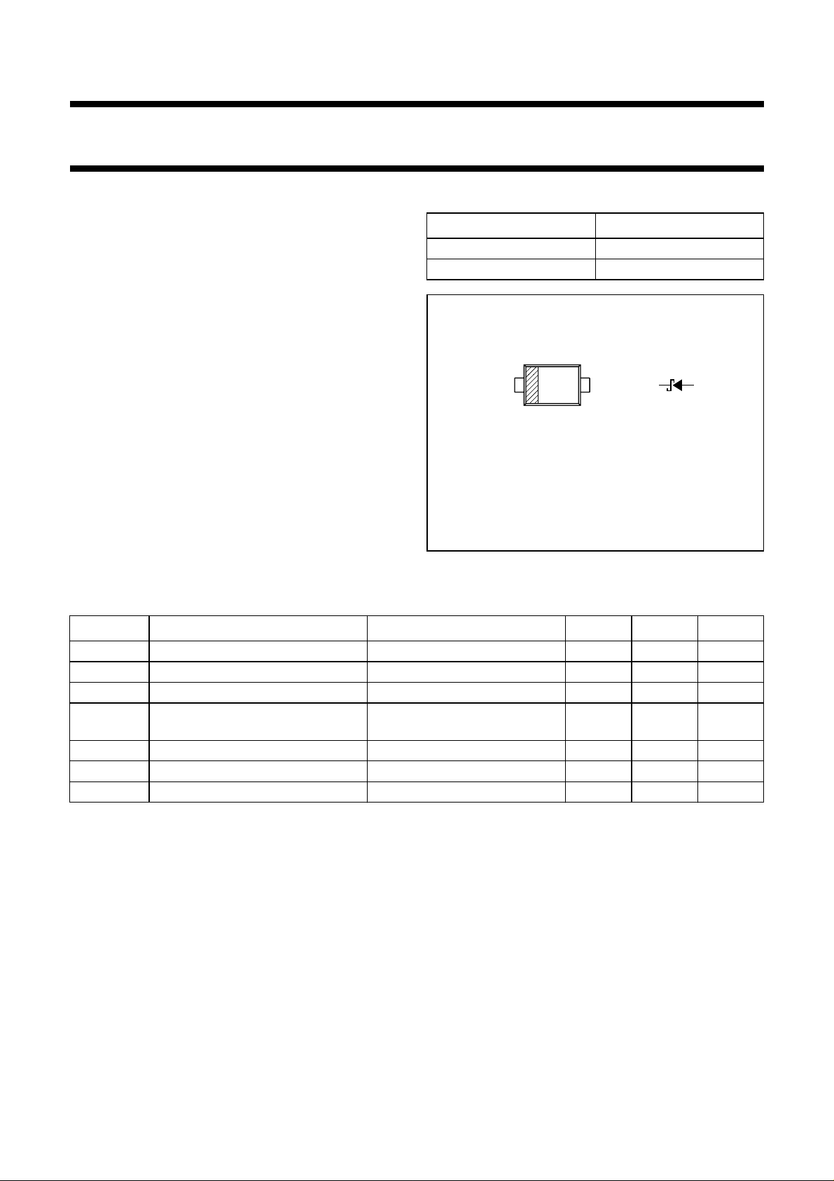
Fig.1 Simplified outline (SC-79; SOD523)
Planar Schottky barrier diode encapsulated in a SC-79
(SOD523) ultra small SMD plastic package.
LIMITING VALUES
In accordance with the Absolute Maximum Rating System (IEC 60134).
PIN DESCRIPTION
1 cathode
2 anode
12
Top view
MGU325
and symbol.
SYMBOL PARAMETER CONDITIONS MIN. MAX. UNIT
V
I
F
I
FRM
I
FSM
R
continuous reverse voltage − 40 V
continuous forward current − 200 mA
repetitive peak forward current tp≤ 1s;δ≤0.5 − 300 mA
non-repetitive peak forward current t = 8.3 ms half sinewave;
− 1A
JEDEC method
T
stg
T
j
T
amb
storage temperature −65 +150 °C
junction temperature − 150 °C
operating ambient temperature −65 +150 °C
2001 Feb 20 2

Philips Semiconductors Product specification
Schottky barrier diode 1PS79SB30
ELECTRICAL CHARACTERISTICS
T
=25°C unless otherwise specified.
amb
SYMBOL PARAMETER CONDITIONS TYP. MAX. UNIT
V
F
I
R
C
d
Note
1. Pulse test: pulse width = 300 µs; δ = 0.02.
forward voltage see Fig.2
I
= 0.1 mA 190 220 mV
F
I
= 1 mA 250 290 mV
F
= 10 mA 320 360 mV
I
F
I
= 100 mA 440 500 mV
F
= 200 mA 520 600 mV
I
F
continuous reverse current VR= 25 V; note 1; see Fig.3 − 0.5 µA
diode capacitance VR= 1 V; f = 1 MHz; see Fig.4 − 20 pF
THERMAL CHARACTERISTICS
SYMBOL PARAMETER CONDITIONS VALUE UNIT
R
th j-a
thermal resistance from junction to ambient note 1 450 K/W
Note
1. Refer to SC-79 (SOD523) standard mounting conditions.
2001 Feb 20 3
 Loading...