

Philips 1PS70SB16, 1PS70SB15, 1PS70SB14, 1PS70SB10 Datasheet
DISCRETE SEMICONDUCTORS
DATA SH EET
k, halfpage
M3D102
1PS70SB10; 1PS70SB14;
1PS70SB15; 1PS70SB16
Schottky barrier (double) diodes
Product specification
1999 Apr 26
Philips Semiconductors Product specification
Schottky barrier (double) diodes
FEATURES
• Low forward voltage
• Guard ring protected
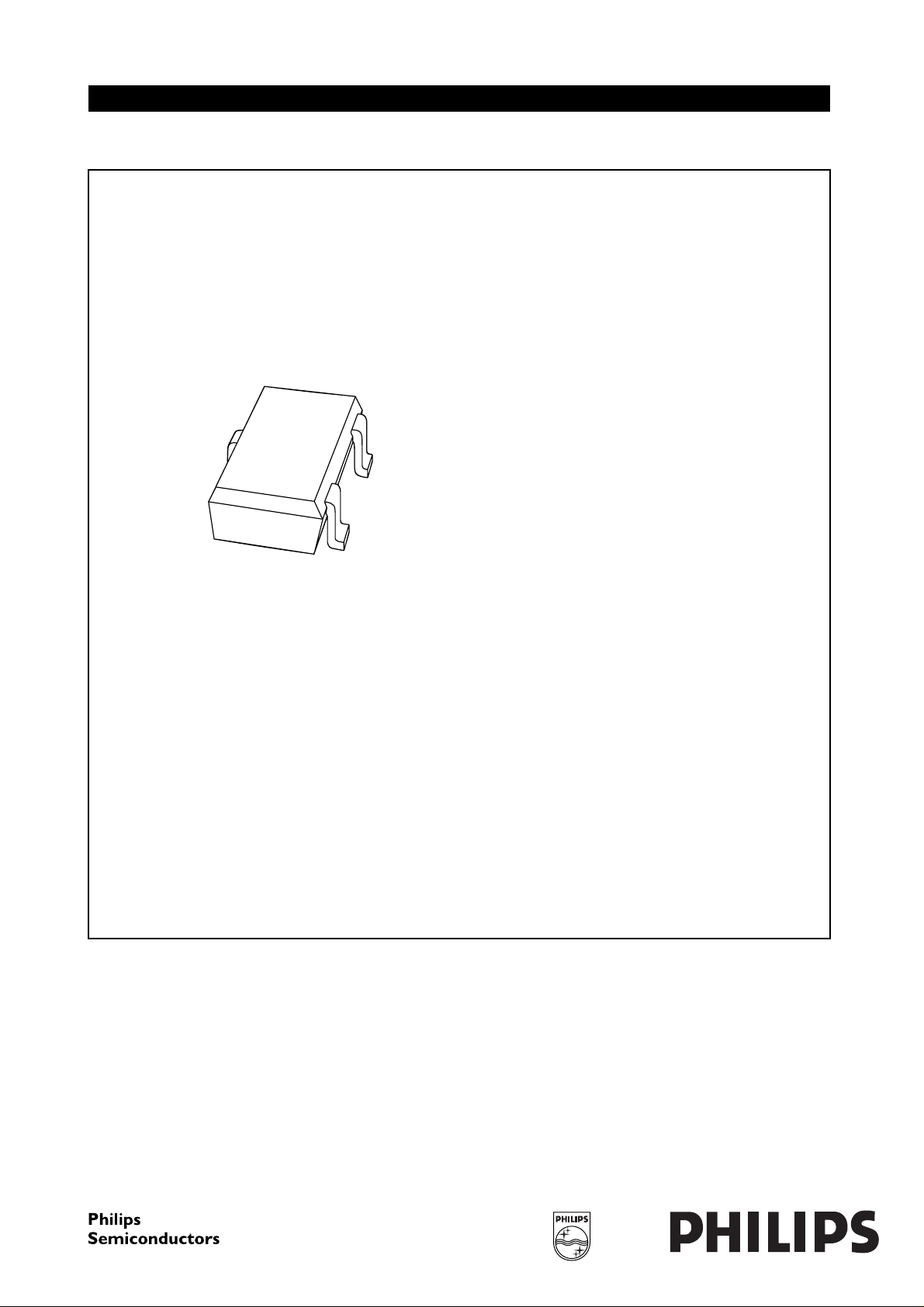
• Very small plastic SMD package.
APPLICATIONS
• Ultra high-speed switching
• Voltage clamping
• Protection circuits
• Blocking diodes.
DESCRIPTION
Planar Schottky barrier diodes
encapsulated in a SOT323 very small
plastic SMD package. Single diodes
and double diodes with different
pinning are available.
MARKING
TYPE NUMBER
MARKING
(1)
CODE
1PS70SB10 7∗0
1PS70SB14 7∗4
1PS70SB15 7∗5
1PS70SB16 7∗6
Note
1. ∗ = -: Made in Hong Kong.
∗ = t: Made in Malaysia.
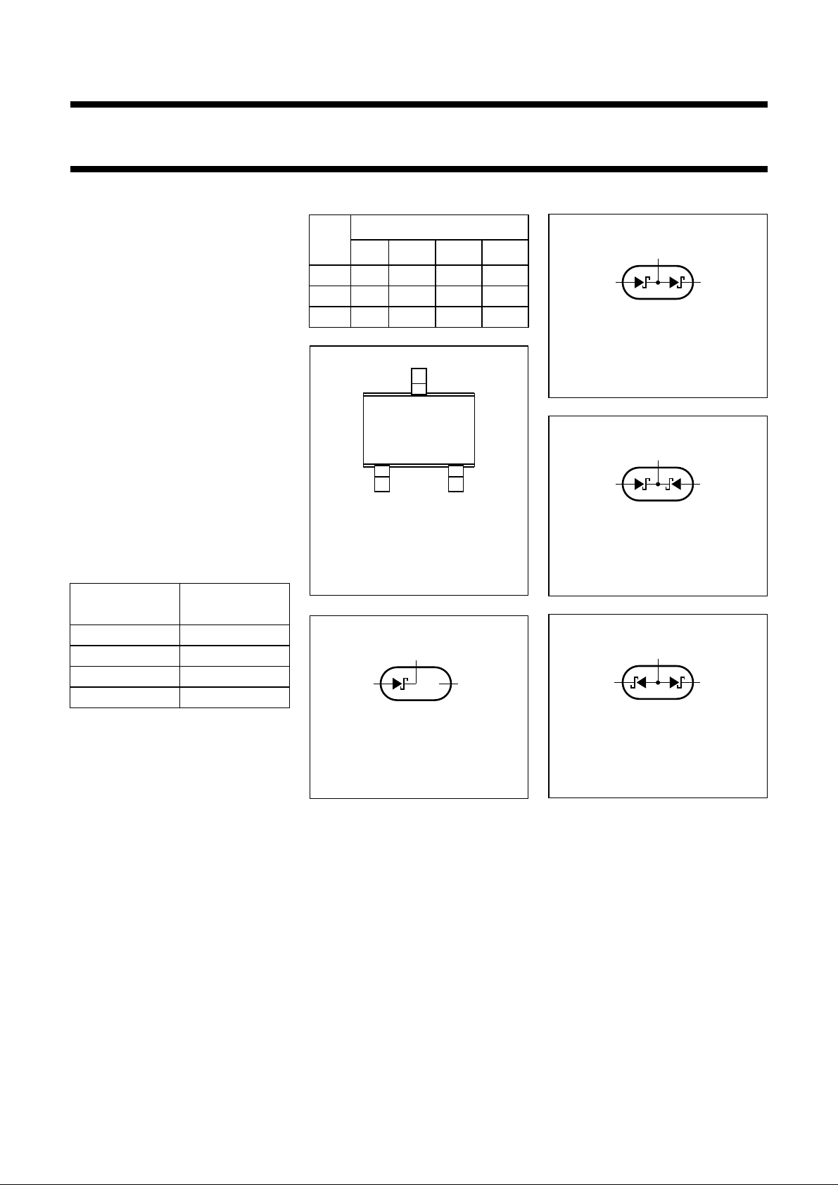
PINNING
PIN
1a
2 n.c. k
3k1k1,a2k1,k2a1,a
alfpage
Fig.1 Simplified outline
Fig.2 1PS70SB10 single
1PS70SB10; 1PS70SB14;
1PS70SB15; 1PS70SB16
1PS70SB..
10 14 15 16
a1a1k
1
a
2
1
Top view
2
3
MGD765
SOT323 (SC-70) and
pin configuration.
3
12
n.c.
MLC357
diode configuration
(symbol).
1
k
2
2
2
3
12
MLC358
Fig.3 1PS70SB14 diode
configuration (symbol).
3
12
MLC359
Fig.4 1PS70SB15 diode
configuration (symbol).
3
12
MLC360
Fig.5 1PS70SB16 diode
configuration (symbol).
1999 Apr 26 2
Philips Semiconductors Product specification
Schottky barrier (double) diodes
1PS70SB10; 1PS70SB14;
1PS70SB15; 1PS70SB16
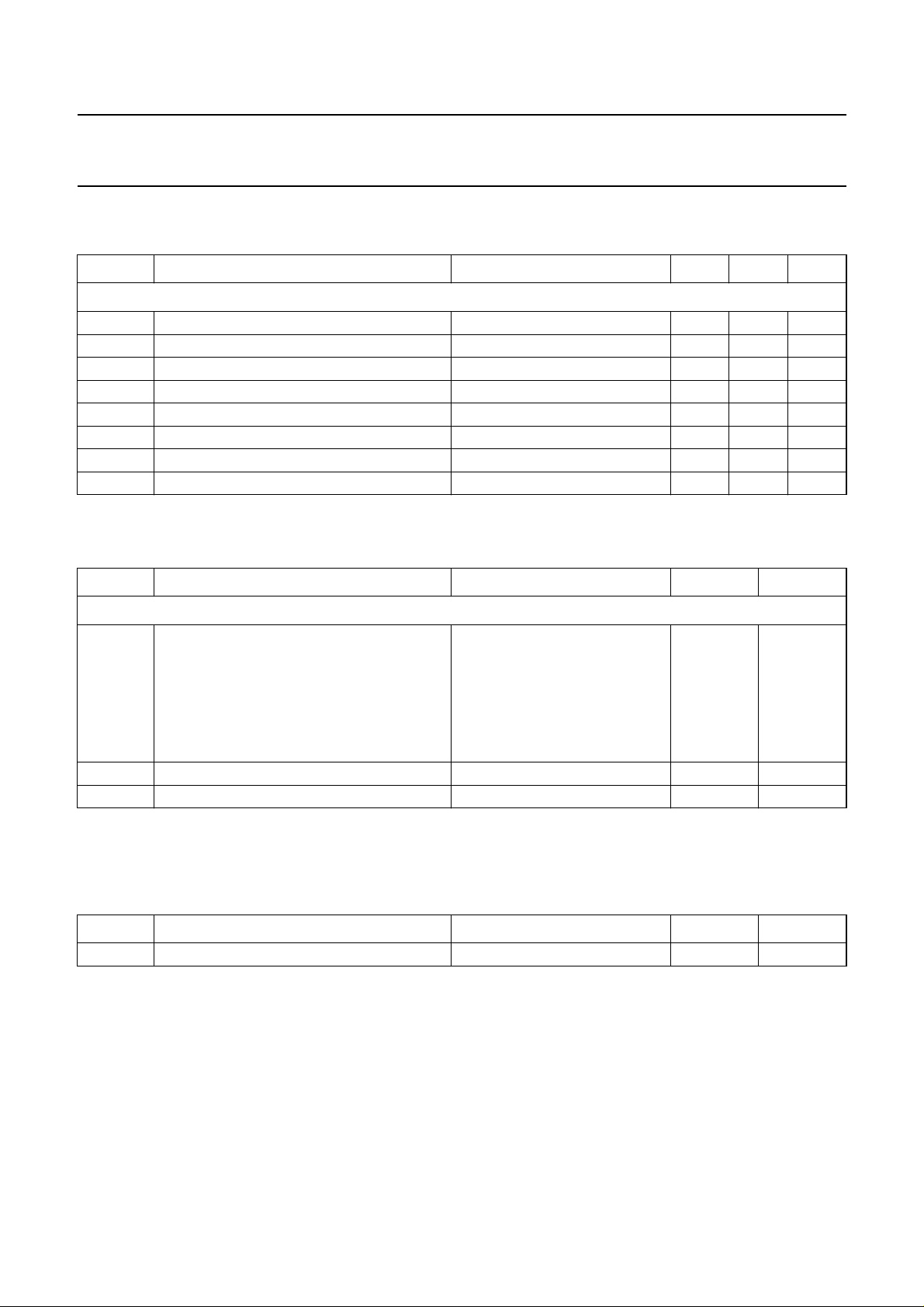
LIMITING VALUES
In accordance with the Absolute Maximum Rating System (IEC 134).
SYMBOL PARAMETER CONDITIONS MIN. MAX. UNIT
Per diode
V
R
I
F
I
FRM
I
FSM
P
tot
T
stg
T
j
T
amb
ELECTRICAL CHARACTERISTICS
T
=25°C unless otherwise specified.
amb
SYMBOL PARAMETER CONDITIONS MAX. UNIT
continuous reverse voltage − 30 V
continuous forward current − 200 mA
repetitive peak forward current tp≤ 1s; δ≤0.5 − 300 mA
non-repetitive peak forward current tp<10ms − 600 mA
total power dissipation (per package) T
<25°C − 200 mW
amb
storage temperature −65 +150 °C
junction temperature − 125 °C
operating ambient temperature −65 +125 °C
Per diode
V
F
I
R
C
d
continuous forward voltage see Fig.6
I
= 0.1 mA 240 mV
F
I
= 1 mA 320 mV
F
= 10 mA 400 mV
I
F
I
= 30 mA 500 mV
F
= 100 mA 800 mV
I
F
continuous reverse current VR= 25 V; note 1; see Fig.7 2 µA
diode capacitance VR= 1 V; f = 1 MHz; see Fig.8 10 pF
Note
1. Pulse test: t
= 300 µs; δ = 0.02.
p
THERMAL CHARACTERISTICS
SYMBOL PARAMETER CONDITIONS VALUE UNIT
R
th j-a
thermal resistance from junction to ambient note 1 625 K/W
Note
1. Refer to SOT323 (SC70) standard mounting conditions.
1999 Apr 26 3
 Loading...