

Philips 1PS59SB21 Datasheet
DISCRETE SEMICONDUCTORS
DATA SH EET
ge
M3D114
1PS59SB21
Schottky barrier diode
Product specification
Supersedes data of 1998 Jul 28
1999 May 05
Philips Semiconductors Product specification
Schottky barrier diode 1PS59SB21
FEATURES
• Ultra fast switching speed
• Low forward voltage
• Guard ring protected
DESCRIPTION
Planar Schottky barrier diode with an
integrated guard ring for stress
protection in an SC-59 small plastic
SMD package.
• Small SMD package.
APPLICATIONS
• High-speed switching
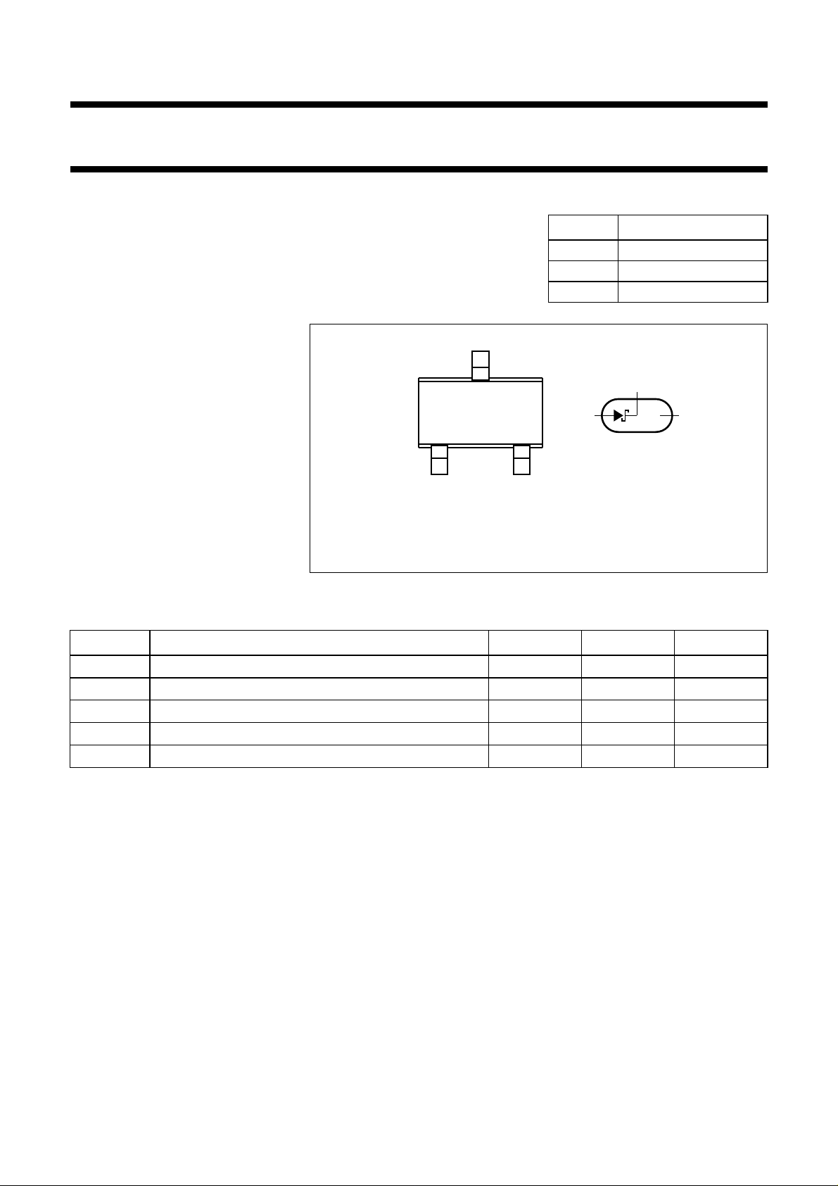
handbook, halfpage
• Voltage clamping
• Protection circuits.
Top view
Marking code: 21.
Fig.1 Simplified outline (SC-59) and symbol.
LIMITING VALUES
In accordance with the Absolute Maximum Rating System (IEC 134).
PINNING
PIN DESCRIPTION
1 anode
2 not connected
3 cathode
3
3
12
n.c.
MLC357
21
MSA314
SYMBOL PARAMETER MIN. MAX. UNIT
V
R
I
F
I
FSM
T
stg
T
j
continuous reverse voltage
continuous forward current −
non-repetitive peak forward current
storage temperature
junction temperature
−
−
−65
−
40 V
200 mA
1A
+150 °C
125 °C
1999 May 05 2

Philips Semiconductors Product specification
Schottky barrier diode 1PS59SB21
ELECTRICAL CHARACTERISTICS
T
=25°C unless otherwise specified.
j
SYMBOL PARAMETER CONDITIONS MIN. MAX. UNIT
V
F
I
R
C
d
Note
1. Pulse test: t
THERMAL CHARACTERISTICS
forward voltage see Fig.2
I
=10mA
F
= 100 mA
I
F
= 200 mA
I
F
reverse current VR= 30 V; note 1; see Fig.3
=30V;Tj= 100 °C; note 1; see Fig.3
V
R
diode capacitance f = 1 MHz; VR= 0; see Fig.4
= 300 µs; δ = 0.02.
p
− 300 mV
− 420 mV
− 550 mV
− 15
− 3
µA
mA
40 50 pF
SYMBOL PARAMETER CONDITIONS VALUE UNIT
R
th j-a
thermal resistance from junction to ambient note 1 500 K/W
Note
1. Refer to SC-59 standard mounting conditions.
1999 May 05 3
 Loading...