

Philips 1N5266B, 1N5265B, 1N5264B, 1N5263B, 1N5261B Datasheet
...
DISCRETE SEMICONDUCTORS
DATA SH EET
M3D176
1N5225B to 1N5267B
Voltage regulator diodes
Product specification
Supersedes data of April 1992
1996 Apr 26
Philips Semiconductors Product specification
Voltage regulator diodes 1N5225B to 1N5267B
FEATURES
• Total power dissipation:
max. 500 mW
• Tolerance series: ±5%
DESCRIPTION
Low-power voltage regulator diodes in hermetically sealed leaded glass
SOD27 (DO-35) packages.
The series consists of 43 types with nominal working voltages from 3.0 to 75 V.
• Working voltage range:
nom. 3.0 to 75 V
• Non-repetitive peak reverse power
dissipation: max. 40 W.
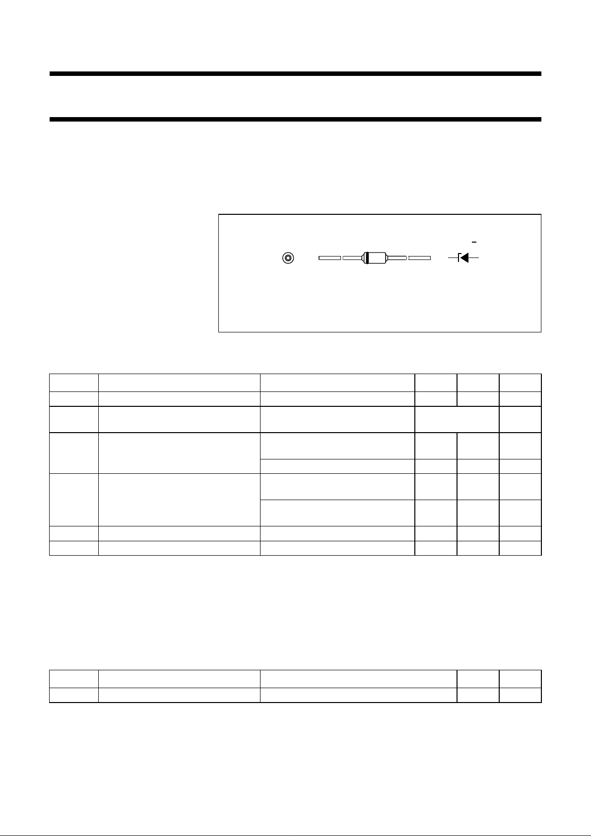
handbook, halfpage
APPLICATIONS
ka
MAM239
• Low-power voltage stabilizers or
voltage references.
The diodes are type branded.
Fig.1 Simplified outline (SOD27; DO-35) and symbol.
LIMITING VALUES
In accordance with the Absolute Maximum Rating System (IEC 134).
SYMBOL PARAMETER CONDITIONS MIN. MAX. UNIT
I
F
I
ZSM
P
tot
continuous forward current − 250 mA
non-repetitive peak reverse current tp= 100 µs; square wave;
Tj=25°C prior to surge
total power dissipation T
=50°C; lead length max.;
amb
see Table
“Per type”
− 400 mW
note 1
Lead length 8 mm; note 2 − 500 mW
P
ZSM
non-repetitive peak reverse power
dissipation
tp= 100 µs; square wave;
Tj=25°C prior to surge; see Fig.3
t
= 8.3 ms; square wave;
p
− 40 W
− 10 W
Tj≤ 55 °C prior to surge
T
stg
T
j
storage temperature −65 +200 °C
junction temperature −65 +200 °C
Notes
1. Device mounted on a printed circuit-board without metallization pad.
2. Tie-point temperature ≤ 75 °C.
ELECTRICAL CHARACTERISTICS
Table 1
=25°C; unless otherwise specified.
T
j
SYMBOL PARAMETER CONDITIONS MAX. UNIT
V
F
forward voltage IF= 200 mA; see Fig.4 1.1 V
1996 Apr 26 2
1996 Apr 26 3
Per type
=25°C; unless otherwise specified.
T
j
Philips Semiconductors Product specification
Voltage regulator diodes 1N5225B to 1N5267B
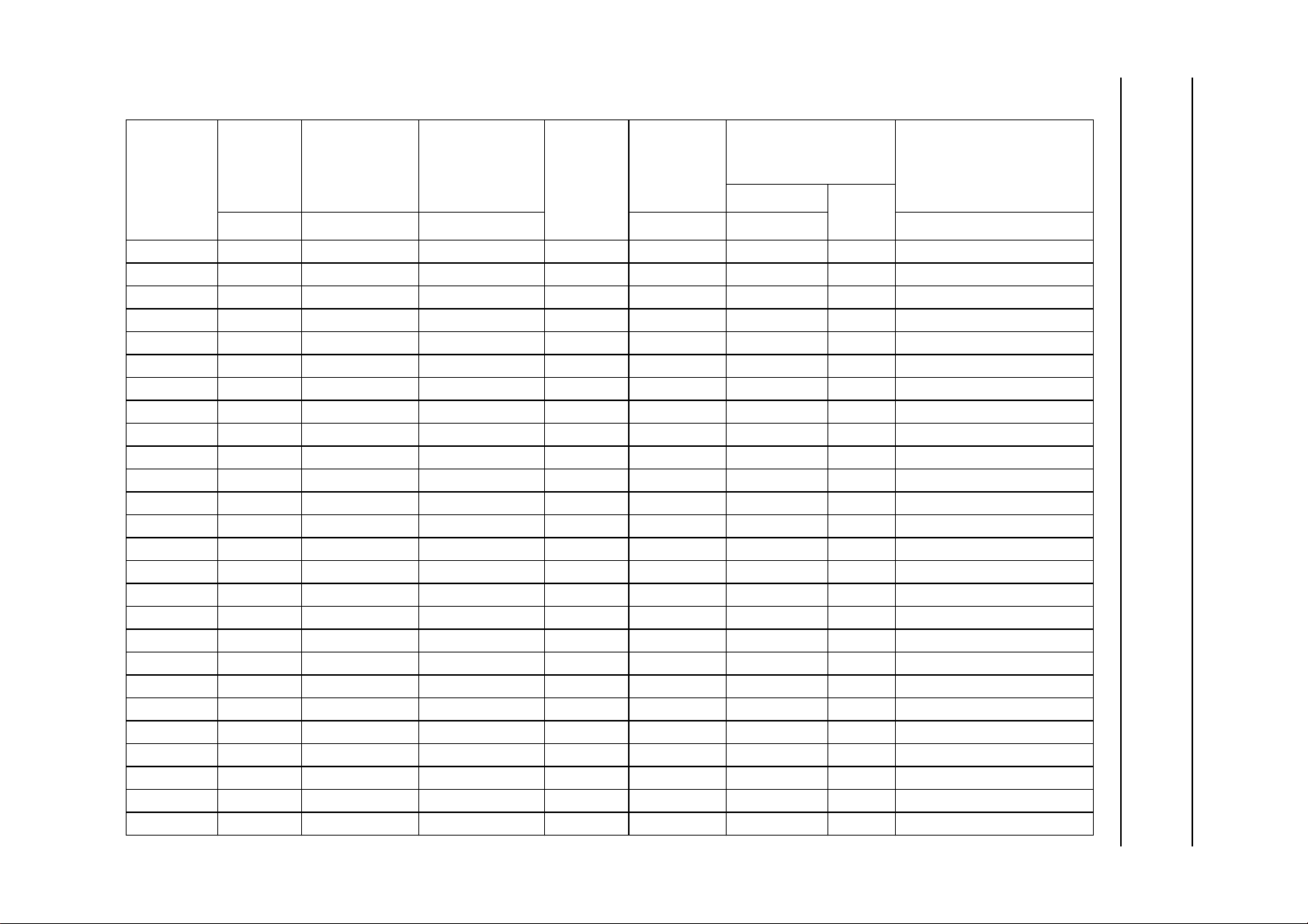
TYPE No.
WORKING
VOLTAGE
(1)
(V)
V
Z
at I
Ztest
DIFFERENTIAL
RESISTANCE
(Ω)
r
dif
at I
Ztest
TEMP. COEFF.
(%/K)
S
Z
(2)
at I
Z
TEST
CURRENT
(mA)
I
Ztest
DIODE CAP.
Cd(pF)
at f = 1 MHz;
at VR=0V
NOM. MAX. MAX. MAX. MAX. MAX.
REVERSE CURRENT
at REVERSE
VOLTAGE
IR (µA)
V
R
(V)
NON-REPETITIVE PEAK
REVERSE CURRENT
tp= 100 µs; T
1N5225B 3.0 1600 −0.075 20 450 50 1.0 6.0
1N5226B 3.3 1600 −0.070 20 450 25 1.0 6.0
1N5227B 3.6 1700 −0.065 20 450 15 1.0 6.0
1N5228B 3.9 1900 −0.060 20 450 10 1.0 6.0
1N5229B 4.3 2000 ±0.055 20 450 5 1.0 6.0
1N5230B 4.7 1900 ±0.030 20 450 5 1.5 6.0
1N5231B 5.1 1600 ±0.030 20 300 5 2.0 6.0
1N5232B 5.6 1600 +0.038 20 300 5 3.0 6.0
1N5233B 6.0 1600 +0.038 20 300 5 3.5 6.0
1N5234B 6.2 1000 +0.045 20 200 5 4.0 6.0
1N5235B 6.8 750 +0.050 20 200 3 5.0 6.0
1N5236B 7.5 500 +0.058 20 150 3 6.0 4.0
1N5237B 8.2 500 +0.062 20 150 3 6.5 4.0
1N5238B 8.7 600 +0.065 20 150 3 6.5 3.5
1N5239B 9.1 600 +0.068 20 150 3 7.0 3.0
1N5240B 10 600 +0.075 20 90 3 8.0 3.0
1N5241B 11 600 +0.076 20 85 2 8.4 2.5
1N5242B 12 600 +0.077 20 85 1 9.1 2.5
1N5243B 13 600 +0.079 9.5 80 0.5 9.9 2.5
1N5244B 14 600 +0.082 9.0 80 0.1 10.0 2.0
1N5245B 15 600 +0.082 8.5 75 0.1 11.0 2.0
1N5246B 16 600 +0.083 7.8 75 0.1 12.0 1.5
1N5247B 17 600 +0.084 7.4 75 0.1 13.0 1.5
1N5248B 18 600 +0.085 7.0 70 0.1 14.0 1.5
1N5249B 19 600 +0.086 6.6 70 0.1 14.0 1.5
1N5250B 20 600 +0.086 6.2 60 0.1 15.0 1.5
I
ZSM
(A)
amb
=25°C
 Loading...