Philips 19PFL4322/45 Schematic

Colour Television Chassis
TPS1.0L
LA
19PFL4322/45
H_17350_000.eps
Contents Page Contents Page
1 Technical Specifications, Connections, and Chassis
Overview 2
2 Safety Instructions, Warnings, and Notes 5
3 Directions for Use 7
4 Mechanical Instructions 8
5 Service Modes, Error Codes, and Fault Finding 12
6 Block Diagrams, Test Point Overview, and
Waveforms
Wiring Diagram 18
Block Diagrams 19-21
7 Circuit Diagrams and PWB Layouts Diagram
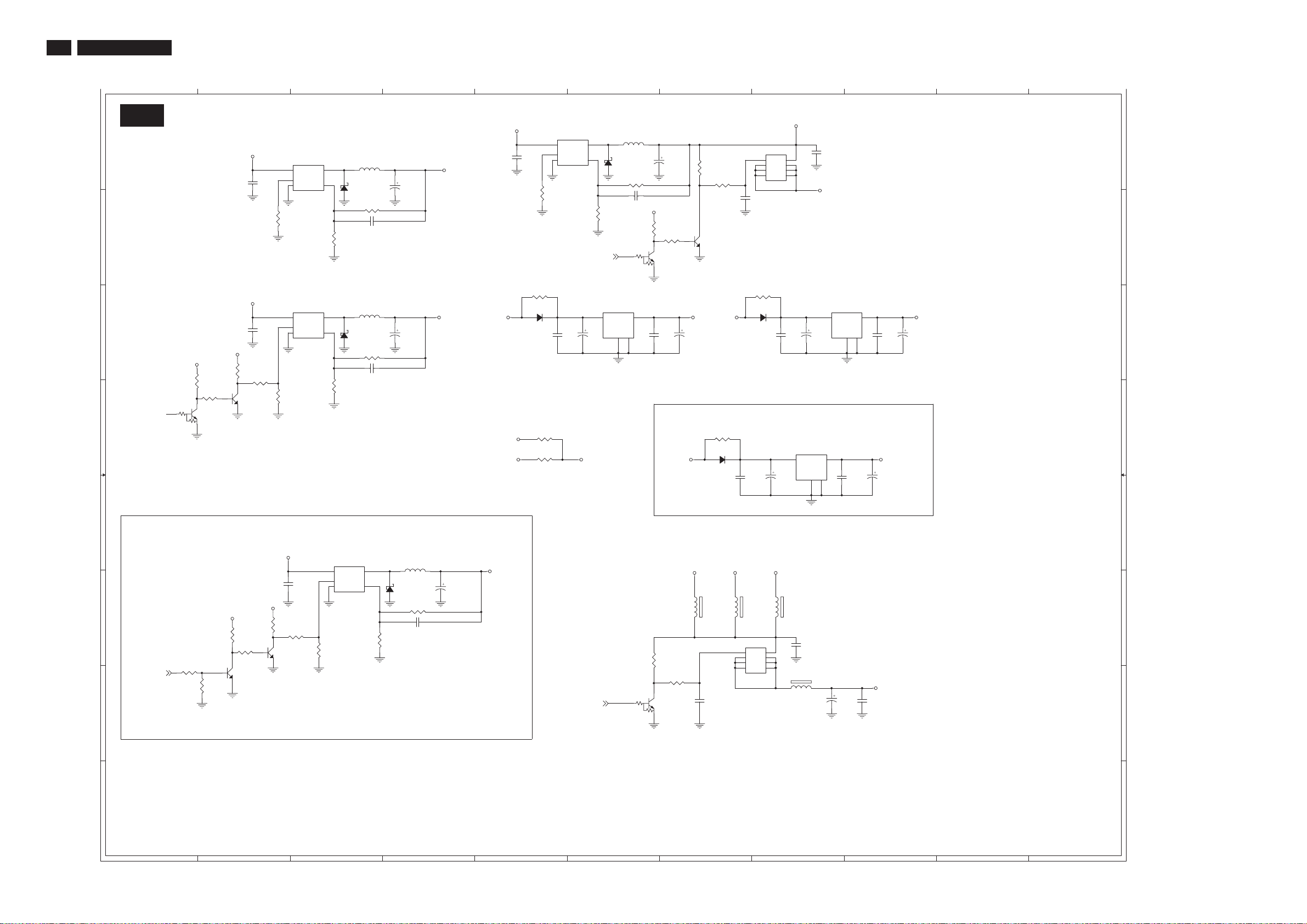
Scaler Board: DC - DC Power (S-01) 22
Scaler Board: Lips & Inverter I/F (S-02) 23
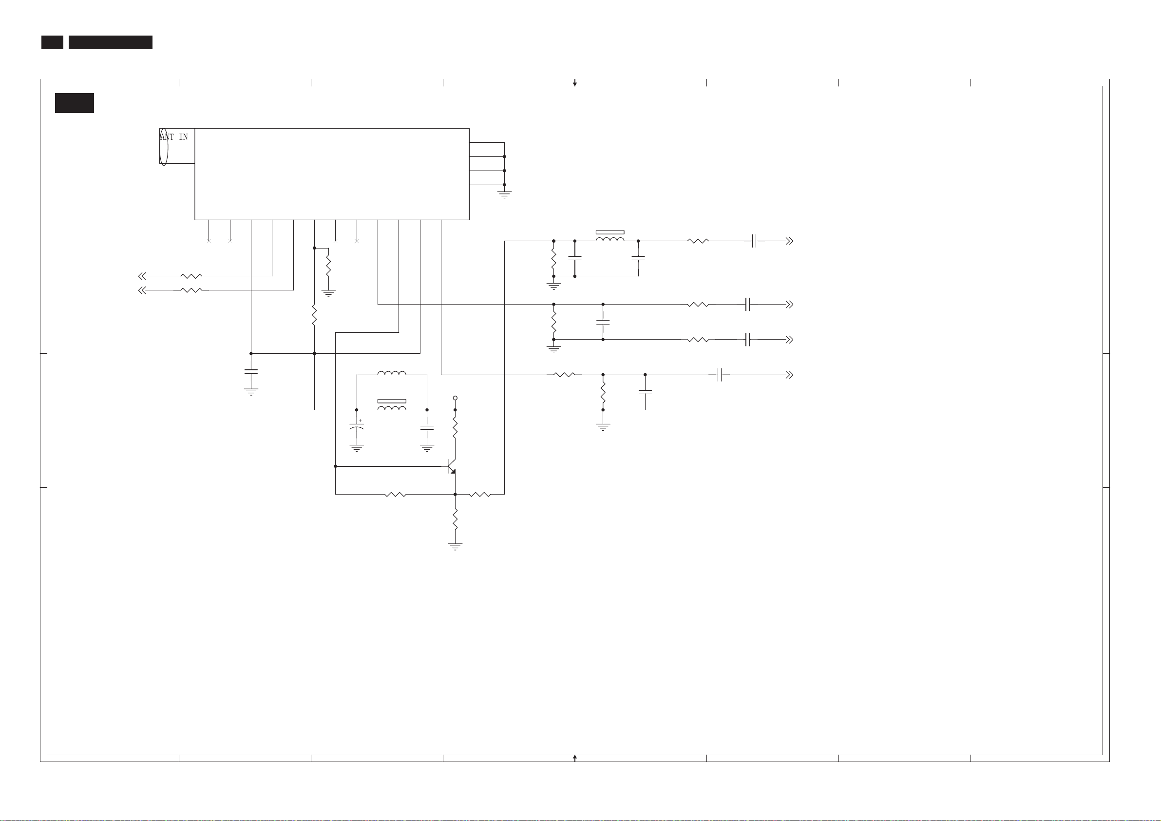
Scaler Board: Tuner (S-03) 24
Scaler Board: Video Inputs (S-04) 25
Scaler Board: DSUB Input (S-05) 26
Scaler Board: DVI-D Input (S-06) 27
Scaler Board: MST96885LD/ALD (S-07) 28
Scaler Board: Flash ROM & SDRAM (S-08) 29
Scaler Board: Key, IR BD & ComPair I/F (S-09) 30
Scaler Board: ITV I/F (S-10) 31
Scaler Board: Panel I/F (S-11) 32
Scaler Board: Audio I/F (S-12) 33
Scaler Board: Audio Amplifier (S-13) 34
Waveform Diagram 45-47
Power Panel (P-01) 48
Power Panel (P-02) 49
Keyboard Control Panel (K) 52
IR & LED Panel (I) 55
Side AV Board (SA) 58
8 Alignments 61
9 Circuit Descriptions, Abbreviation List, and IC Data
Sheets 66
Abbreviation List 69
IC Data Sheets 72
10 Spare Parts List 76
11 Revision List 82
081007
©
Copyright 2007 Philips Consumer Electronics B.V. Eindhoven, The Netherlands.
All rights reserved. No part of this publication may be reproduced, stored in a
retrieval system or transmitted, in any form or by any means, electronic,
mechanical, photocopying, or otherwise without the prior permission of Philips.
Published by CS 0771 BU CD Customer Service Printed in the Netherlands Subject to modification EN 3122 785 17351
2
TPS 1.0L LA
1. Technical Specifications,Connections,and Chassis Overview
1.Technical Specifications,Connections,and Chassis Overview
Index of this chapter:
1.1 Technical Specifications
1.2 Connections
1.3 Chassis Overview
Notes:
Figures below can deviate slightly from the actual situation,
due to the different set executions.
Specifications are indicative (subject to change)
1.1 Technical Specifications
1.1.1 Technical Specifications
Panel : LCD
Display area(mm) : 410.4 mm X 256.5 mm
Number of Pixels : 1440(H) x 900(V)
Pitch ( mm ) : 0.285(H) x 0.285 mm(V) (19")
Display operating mode : Normally White
Color depth : 16.2M colors
Brightness (cd/m^2) : 300(Center 1 points, Typ.) Min :
230
Viewing angle(CR>10) : Viewing angle free
(R/L 85/85 (Typ.) ,U/D 80/80(Typ.))
(19")
Surface treatment : Hard coating 3H
Electrical interface : LVDS
Response Time : 5ms (Typ) (19")
Contrast ratio : Typical 850 : 1 Min : 500
Outline Dimension : 427.2 mm(H) x 277.4 mm(V) x
17.0(D) mm (Typ.) (19")
Module weight (g) : 2500g(Typ.) (19")
Backlight : 4 CCFL
Allowed signal mode specified
For 19PFL4322/45
PC timing table
Mode Resolution H. freq. / V. Standard
1 640 x 480 31.469Khz/59.9 VGA
2 800 x 600 35.156Khz/56.2 VESA
3 800 x 600 37.879Khz/60.3 VESA
4 1024 x 768 48.363Khz/60.0 VESA
5 1280 x 720 44.772kHz/59.8 CVT
6 1280 x 768 47.776kHz/59.8 CVT
7 1440 x 900 55.469kHz/59.9 CVT
TV system signal mode:
RF support: Latin PAL M/N, NTSC-M TV tuning systems
CVBS/S-video: Support PAL and NTSC colour system.
Comp video IN(YpbPr) : including 480i/p 60Hz , 576i/p 50Hz,720p
50/60Hz, 1080i 50//59/60Hz. , 1080p 50//59/60Hz
DVI (Video) IN : 480p, 576p, 720p 50/60Hz, 1080i 50/59/60Hz,
1080p 50/59/60Hz
1.1.2 Sound
Sound sy
Maximum power : 2 x 3W
stems : Mono / Stereo / Virtual Surround
1.1.3 Miscellaneous
Power Supply
AC-input : 90V ~ 264VAC, 50/60 2Hz
Power consumption : 70W/Max(at PC mode),70W/Max(at
TV mode) with Audio.
Power cord length 1.8m
Power cord type : European type and China type
Power indicator : LED (On: Blue ,Sleeping mode:
Amber )
Auto power saving : < 2W
Ambient conditions
Temperature : 0 to40°C
Humidity : 10 to 90%
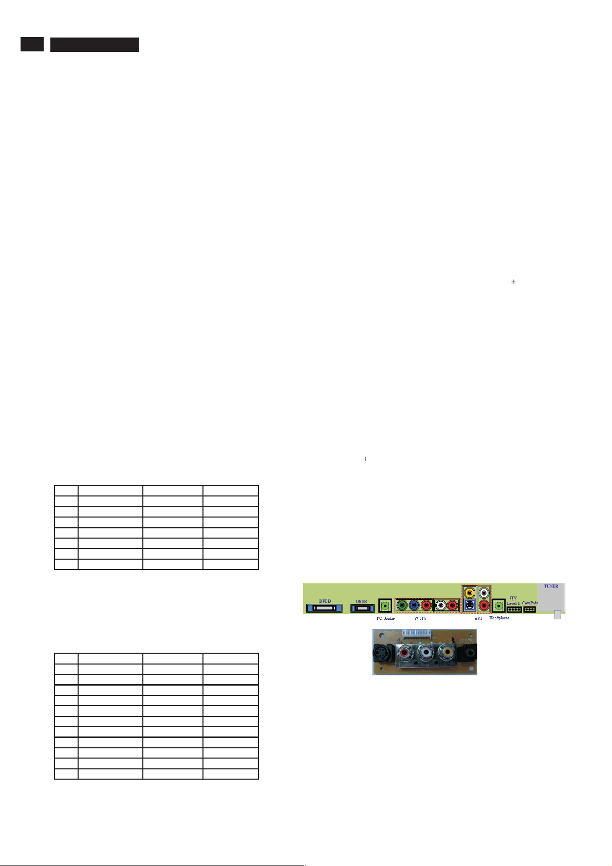
1.2 Connectors
1.2.1 I/O interface
1 Tuner: Latin PAL M/N, NTSC-M TV tuning systems
2 Compair
3 AV1 audio IN : AV1 and S-Video shared audio R/L(RCA jack)
4 AV1 IN : Composite video input (AV1)
5 CVI IN : Component input with YPbPr format with audio R/L.
6 PC audio IN: audio R/L(mini-jack).
7 PC IN: VGA input (D-SUB connectors)
8 DVI-D : digital PC and video input
9 Earphone : earphone jack
10 AV2 IN : Composite video input (AV2 side)
11 AV2 audio IN : AV2 and S-Video side audio R/L(RCA jack)
12 S-Video IN : S-video input (S-Video side)
Rx/Tx communicate
User modes - User timings can be stored by first in first out.
Auto adjustment an be used for optimal picture
performance. 11 video timings are reloaded in
factory prior to other user timings are stored.
User video timing specifications:
Mode Resolution H. freq. / V. Standard
1 640 x 350 31.469Khz/70.0 VGA
2 720 x 400 31.469Khz/70.0 VGA
3 640 x 480 35.000Khz/66.6 Macintosh
4 640 x 480 37.861Khz/72.8 VESA
5 640 x 480 37.500Khz/75.0 VESA
6 800 x 600 48.077Khz/72.1 VESA
7 800 x 600 46.875Khz/75.0 VESA
8 832 x 624 49.700Khz/75.0 Macintosh
9 1024 x 768 56.476Khz/70.0 VESA
10 1024 x 768 60.023Khz/75.0 VESA
11 1360 x 768 47.712kHz/60.0 CVT
1.2.2 PC mode signal type
a.Analog Video : 15 pin D-sub ,0.7 Vp-p linear, positive polarity &
separate sync.( TTL level, positive or negative
polarity)
b.Audio signal : 3.5mm stereo mini-jack
Level: Nominal : 0.5 V rms.
-Maximum :1.5Vrms.
-Impedance > 10 kW.
c.Signal source: Pattern generator format as attachment table 1 to 12.
Reference generator : CHROMA 2200 or QuantumData 802R
TV mode signal type
1. Technical Specifications, Connections and Chassis Overview
TPS 1.0L LA
3
RF Signal: Aerial input / 10mV(typical: 80dBuV; range: 30-100dBuV)
Video signal : CVBS input ( RCA jack) / 1Vpp (300mV-sync,
700mV-video.)
S video input / 1VppY-signal, +/-300mV C-signal
Comp video in(YPbPr input)/ 1Vpp Y signal,
+/-350mV Pb,Pr signal
DVI-D:Digital interface with 4 channels TMDS signal
Audio signal : Audio (1) R/L for AV IN(AV and S-Video).
Level: - Nominal : 0.5 V rms.
- Maximum : 1.5 V rms.
- Impedance > 10 kW.
Audio (2) R/L for SCART IN
Level: - Nominal : 0.5 V rms.
- Maximum : 1.5 V rms.
- Impedance > 10 k W.
Audio (3) Mini-jack audio for DVI
Headphone
Audio: R/L output -10mW at 32W.
3.5mm stereo jack with switch
Impedance is between 8 and 600 W
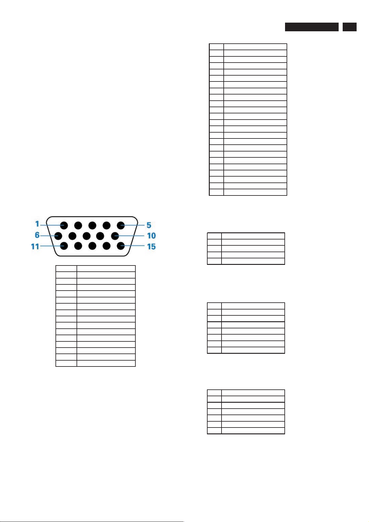
1.2.3 VGA Pin assignment
PIN No. SIGNAL
1 Red video input
2 Green video input /SOG
3 Blue video input
4GND
5 GND– cable detect
6 Red video ground
7 Green video ground
8 Blue video ground
9 DDC +3.3V (or 5V)
10 Logic ground
11 GND
12 Serial data line (SDA)
13 H. Sync / H+V
14 V. Sync
15 Data clock line (SCL)
1.2.4 24-pin DVI-D digital connect of signal cable.
.
1 T.M.D.S. Data22 T.M.D.S. Data2+
3 T.M.D.S. Data2/4 Shield
4 No connect
5 No connect
6 DDC Clock
7 DDC Data
8 No connect
9 T.M.D.S. Data110 T.M.D.S. Data1+
11 T.M.D.S. Data1/3 Shield
12 No connect
13 No connect
14 +5V Power
15 Ground (for +5V)
16 Hot Plug Detect
17 T.M.D.S. Data018 T.M.D.S. Data0+
19 T.M.D.S. Data0/5 Shield
20 No connect
21 No connect
22 T.M.D.S. Clock Shield
23 T.M.D.S. Clock+
24 T.M.D.S. Clock-
1.2.5 CVBS
The input signals are applied to display through CVBS cable
Pin assignment
PIN SIGNAL
1GND
2CVBS
3CVBS
4CVBS
1.2.6 S-Video
The input signals are applied to display through S-Video cable
Pin assignment
PIN SIGNAL
1GND
2GND
3GND
4GND
5GND
6LUMA
7 CHROMA
1.2.7 Component Video
The input signals are applied to display through Component Video
RCA Jack pin assignment
PIN SIGNAL
1GND
2
Red à Pr
3GND
4
Blue à Pb
5GND
6 Green àY
4
TPS 1.0L LA
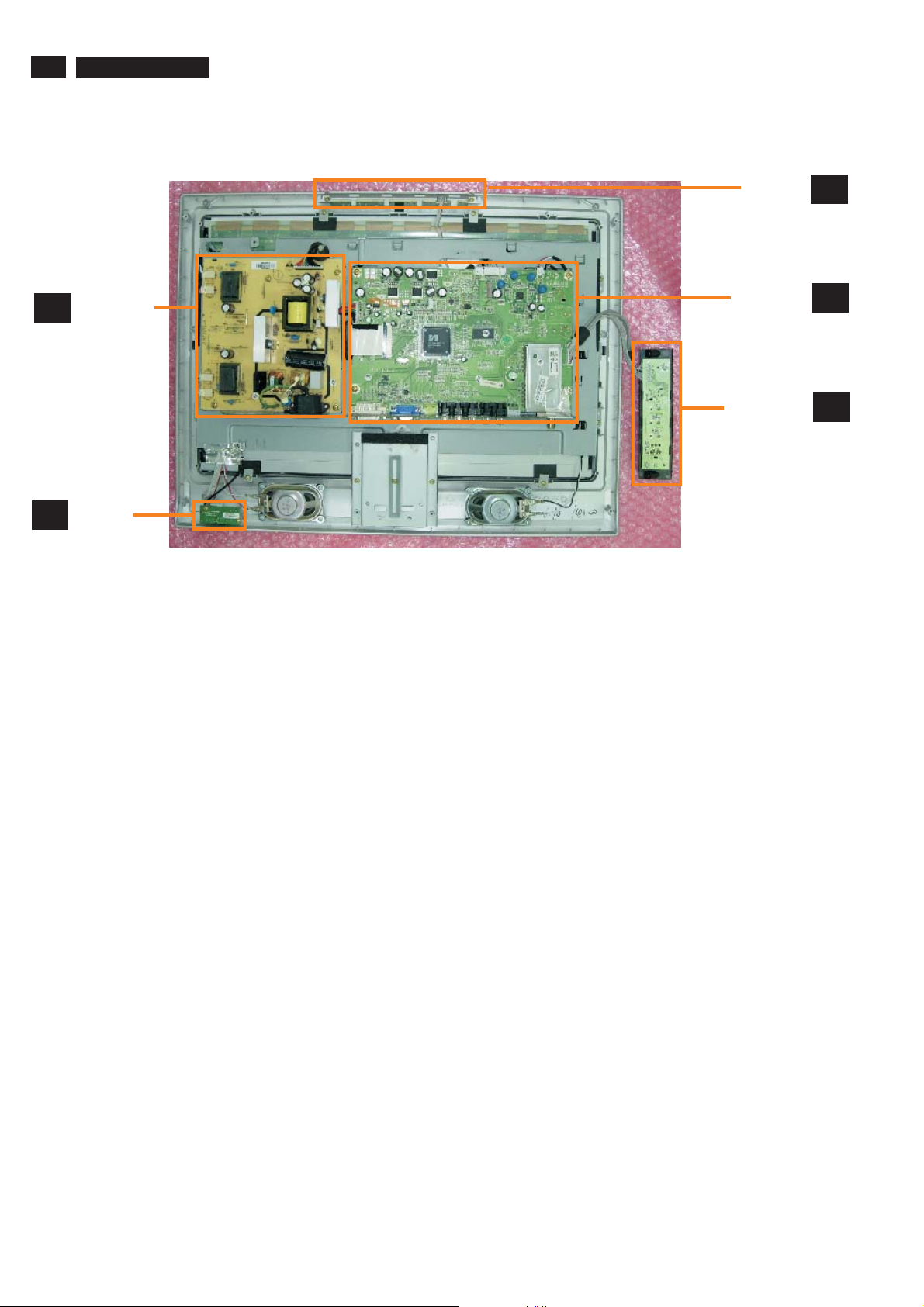
1.3 Chassis Overview
Type: 19PFL4322/45
1. Technical Specifications,Connections,and Chassis Overview
P
I
Power Board
IR Board
Key Board
Scaler Board
Side AV Board
K
S
SA

Safety Instructions, Warnings, and Notes
2. Safety Instructions, Warnings, and Notes
EN 5TPS1.0LLA 2.
Index of this chapter:
2.1 Safety Instructions
2.2 Warnings
2.3 Notes
2.1 Safety Instructions
Safety regulations require the following during a repair:
• Connect the set to the Mains/AC Power via an isolation
transformer (> 800 VA).
• Replace safety components, indicated by the symbol h,
only by components identical to the original ones. Any
other component substitution (other than original type) may
increase risk of fire or electrical shock hazard.
Safety regulations require that after a repair, the set must be
returned in its original condition. Pay in particular attention to
the following points:
• Route the wire trees correctly and fix them with the
mounted cable clamps.
• Check the insulation of the Mains/AC Power lead for
external damage.
• Check the strain relief of the Mains/AC Power cord for
proper function.
• Check the electrical DC resistance between the Mains/AC
Power plug and the secondary side (only for sets that have
a Mains/AC Power isolated power supply):
1. Unplug the Mains/AC Power cord and connect a wire
between the two pins of the Mains/AC Power plug.
2. Set the Mains/AC Power switch to the “on” position
(keep the Mains/AC Power cord unplugged!).
3. Measure the resistance value between the pins of the
Mains/AC Power plug and the metal shielding of the
tuner or the aerial connection on the set. The reading
should be between 4.5 Mohm and 12 Mohm.
4. Switch “off” the set, and remove the wire between the
two pins of the Mains/AC Power plug.
• Check the cabinet for defects, to prevent touching of any
inner parts by the customer.
2.2 Warnings
• All ICs and many other semiconductors are susceptible to
electrostatic discharges (ESD w). Careless handling
during repair can reduce life drastically. Make sure that,
during repair, you are connected with the same potential as
the mass of the set by a wristband with resistance. Keep
components and tools also at this same potential.
• Be careful during measurements in the high voltage
section.
• Never replace modules or other components while the unit
is switched “on”.
• When you align the set, use plastic rather than metal tools.
This will prevent any short circuits and the danger of a
circuit becoming unstable.
2.3 Notes
2.3.1 General
• Measure the voltages and waveforms with regard to the
chassis (= tuner) ground (H), or hot ground (I), depending
on the tested area of circuitry. The voltages and waveforms
shown in the diagrams are indicative. Measure them in the
Service Default Mode (see chapter 5) with a colour bar
signal and stereo sound (L: 3 kHz, R: 1 kHz unless stated
otherwise) and picture carrier at 475.25 MHz for PAL, or
61.25 MHz for NTSC (channel 3).
• Where necessary, measure the waveforms and voltages
with (D) and without (E) aerial signal. Measure the
voltages in the power supply section both in normal
operation (G) and in stand-by (F). These values are
indicated by means of the appropriate symbols.
• Manufactured under license from Dolby Laboratories.
“Dolby”, “Pro Logic” and the “double-D symbol”, are
trademarks of Dolby Laboratories.
2.3.2 Schematic Notes
• All resistor values are in ohms, and the value multiplier is
often used to indicate the decimal point location (e.g. 2K2
indicates 2.2 kohm).
• Resistor values with no multiplier may be indicated with
either an “E” or an “R” (e.g. 220E or 220R indicates 220
ohm).
• All capacitor values are given in micro-farads (μ= × 10
nano-farads (n= × 10
• Capacitor values may also use the value multiplier as the
decimal point indication (e.g. 2p2 indicates 2.2 pF).
• An “asterisk” (*) indicates component usage varies. Refer
to the diversity tables for the correct values.
• The correct component values are listed in the Spare Parts
List. Therefore, always check this list when there is any
doubt.
2.3.3 BGA (Ball Grid Array) ICs
Introduction
For more information on how to handle BGA devices, visit this
URL: www.atyourservice.ce.philips.com (needs subscription,
not available for all regions). After login, select “Magazine”,
then go to “Repair downloads”. Here you will find Information
on how to deal with BGA-ICs.
BGA Temperature Profiles
For BGA-ICs, you must use the correct temperature-profile,
which is coupled to the 12NC. For an overview of these profiles,
visit the website www.atyourservice.ce.philips.com (needs
subscription, but is not available for all regions)
You will find this and more technical information within the
“Magazine”, chapter “Repair downloads”.
For additional questions please contact your local repair help
desk.
2.3.4 Lead-free Soldering
Due to lead-free technology some rules have to be respected
by the workshop during a repair:
• Use only lead-free soldering tin Philips SAC305 with order
code 0622 149 00106. If lead-free solder paste is required,
please contact the manufacturer of your soldering
equipment. In general, use of solder paste within
workshops should be avoided because paste is not easy to
store and to handle.
• Use only adequate solder tools applicable for lead-free
soldering tin. The solder tool must be able:
– To reach a solder-tip temperature of at least 400°C.
– To stabilize the adjusted temperature at the solder-tip.
– To exchange solder-tips for different applications.
• Adjust your solder tool so that a temperature of around
360°C - 380°C is reached and stabilized at the solder joint.
Heating time of the solder-joint should not exceed ~ 4 sec.
Avoid temperatures above 400°C, otherwise wear-out of
tips will increase drastically and flux-fluid will be destroyed.
To avoid wear-out of tips, switch “off” unused equipment or
reduce heat.
• Mix of lead-free soldering tin/parts with leaded soldering
tin/parts is possible but PHILIPS recommends strongly to
-9
), or pico-farads (p= × 10
-12
-6
),
).
EN 6 TPS1.0L LA3.
Directions for Use
avoid mixed regimes. If this cannot be avoided, carefully
clear the solder-joint from old tin and re-solder with new tin.
2.3.5 Alternative BOM identification
The third digit in the serial number (example:
AG2B0335000001) indicates the number of the alternative
B.O.M. (Bill Of Materials) that has been used for producing the
specific TV set. In general, it is possible that the same TV
model on the market is produced with e.g. two different types
of displays, coming from two different suppliers. This will then
result in sets which have the same CTN (Commercial Type
Number; e.g. 28PW9515/12) but which have a different B.O.M.
number.
By looking at the third digit of the serial number, one can
identify which B.O.M. is used for the TV set he is working with.
If the third digit of the serial number contains the number “1”
(example: AG1B033500001), then the TV set has been
manufactured according to B.O.M. number 1. If the third digit is
a “2” (example: AG2B0335000001), then the set has been
produced according to B.O.M. no. 2. This is important for
ordering the correct spare parts!
For the third digit, the numbers 1...9 and the characters A...Z
can be used, so in total: 9 plus 26= 35 different B.O.M.s can be
indicated by the third digit of the serial number.
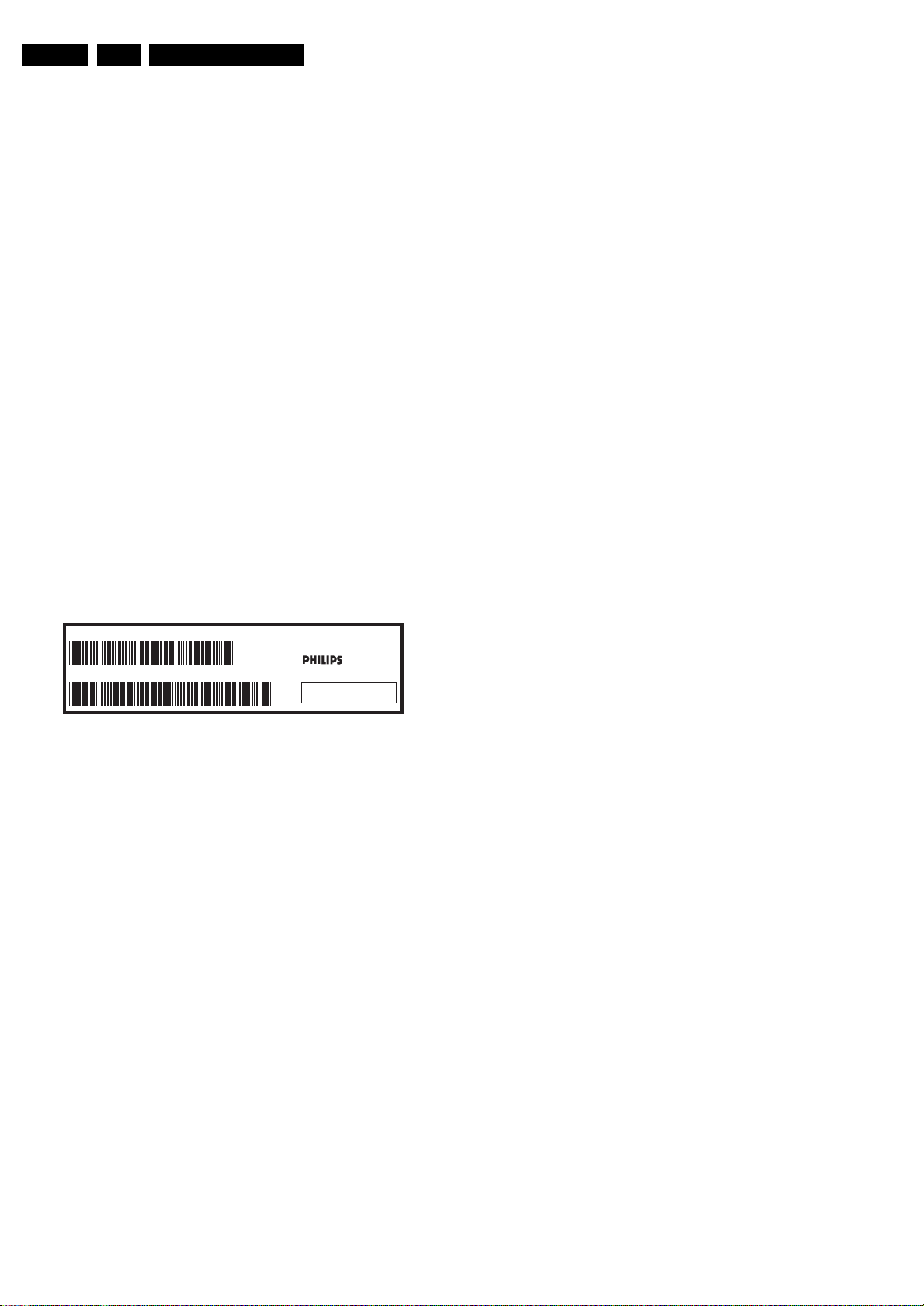
Identification: The bottom line of a type plate gives a 14-digit
serial number. Digits 1 and 2 refer to the production center (e.g.
AG is Bruges), digit 3 refers to the B.O.M. code, digit 4 refers
to the Service version change code, digits 5 and 6 refer to the
production year, and digits 7 and 8 refer to production week (in
example below it is 2006 week 17). The 6 last digits contain the
serial number.
3. Directions for Use
You can download this information from the following websites:
http://www.philips.com/support
http://www.p4c.philips.com
MODEL :
PROD.NO:
2.3.6 Board Level Repair (BLR) or Component Level Repair
(CLR)
If a board is defective, consult your repair procedure to decide
if the board has to be exchanged or if it should be repaired on
component level.
If your repair procedure says the board should be exchanged
completely, do not solder on the defective board. Otherwise, it
cannot be returned to the O.E.M. supplier for back charging!
2.3.7 Practical Service Precautions
• It makes sense to avoid exposure to electrical shock.
• Always respect voltages. While some may not be
32PF9968/10
AG 1A0617 000001
Figure 2-1 Serial number (example)
While some sources are expected to have a possible
dangerous impact, others of quite high potential are of
limited current and are sometimes held in less regard.
dangerous in themselves, they can cause unexpected
reactions that are best avoided. Before reaching into a
powered TV set, it is best to test the high voltage insulation.
It is easy to do, and is a good service precaution.
MADE IN BELGIUM
220-240V 50/60Hz
~
VHF+S+H+UHF
BJ3.0E LA
S
E_06532_024.eps
128W
130606

3. Directions for Use
Refer to page 6.
3. Directions for Use
TPS 1.0E LA
7
8
TPS 1.0L LA
4. Mechanical Instructions
4. Mechanical Instructions
Index of this chapter:
4.1 Assy/Panel Removal
4.2 Set Re-assembly
4.1 Assy/Panel Removal
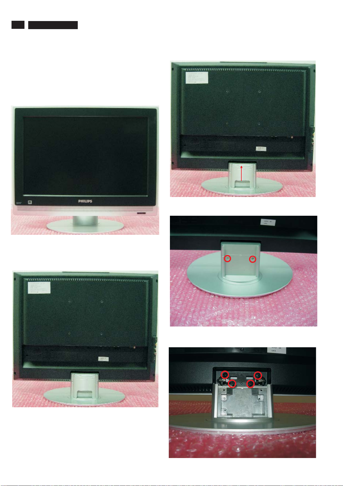
Note:Please put your mechine on a soft material to avoid to
scrape panel when you disassemble it.
Front view
Step 1. Remove the Base.
a. Remove the 2 screws as Fig.3~4.
b. Remove the 4 screws as Fig.5.
Fig.3
Back view
Fig.1
Fig.4
Fig.2
Fig.5
4. Mechanical Instructions
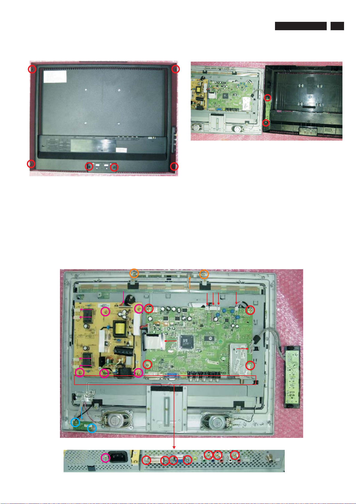
Step 2. Remove the Back cover.
a.
Remove the 6 screws .
b. Remove the 2 screws emove the back cover as Fig.7.
as Fig.6
, then r
Fig.6
Fig.7
TPS 1.0L LA
9
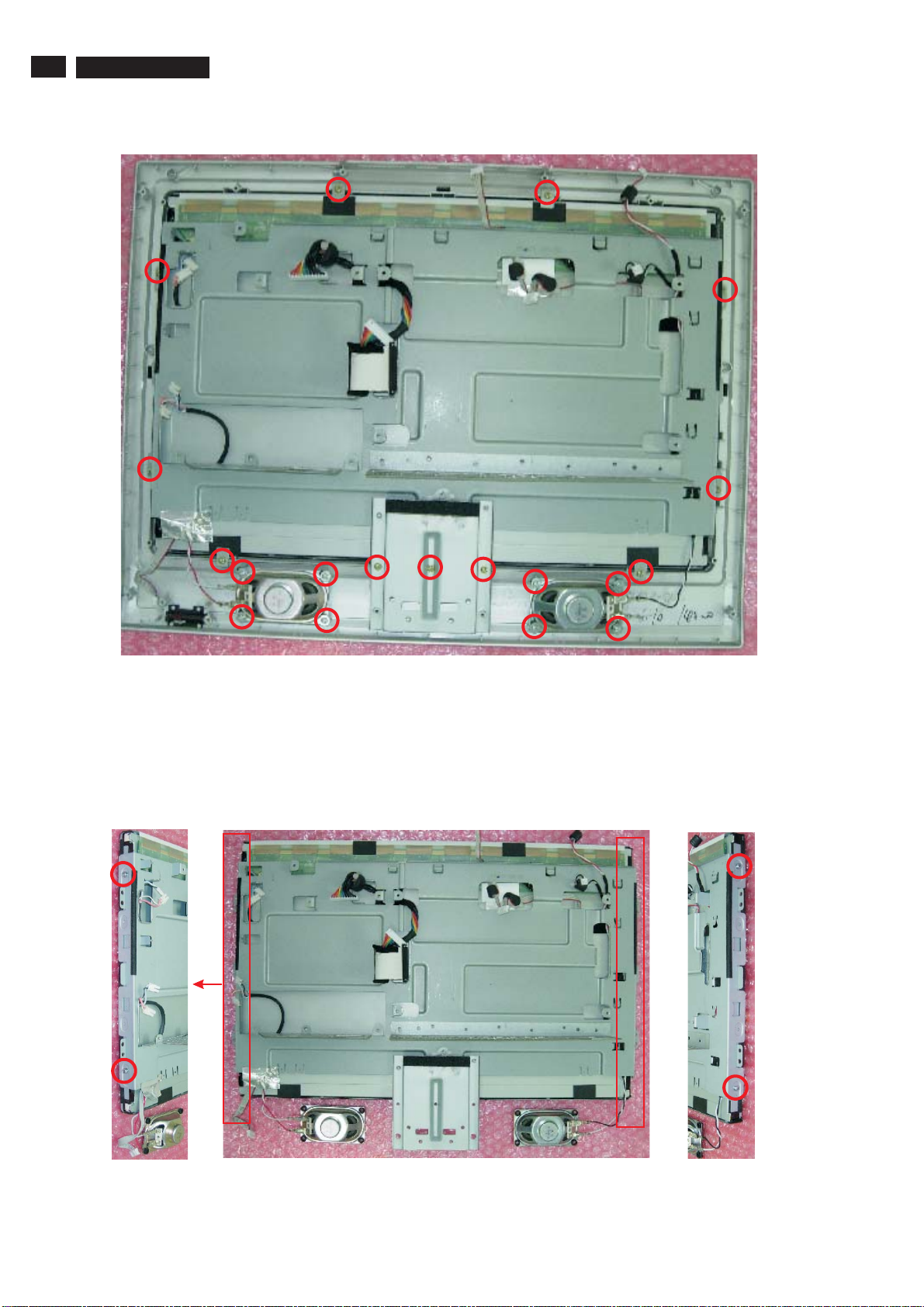
Step 3. Remove the Scaler, Power, IR ,Side AV and Key board as Fig.8 .
a. Remove the 11 screws and disconnect the 6 cables to remove the
scaler and Side AV board .
b. Remove the 6 screws and disconnect the 5 cables to remove the
Power board.
c. Remove the 2 screws and disconnect the 1 cable to remove the IR
board.
d. Remove the 2 screws and disconnect the 1 cable to remove the Key
board.
Fig.8
10
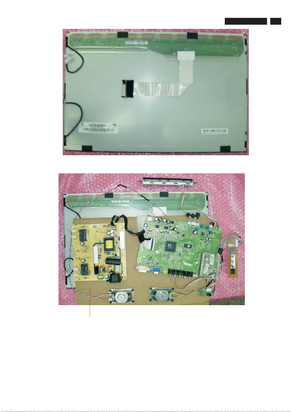
Step 4. Remove the Front bezel as Fig.9.
a. Remove the 19 screws to remove the Front bezel as Fig.9.
TPS 1.0L LA
4. Mechanical Instructions
Step 5. Remove the Frame assy as Fig.10~11.
Remove the 4 screws
a. as Fig.10.
b. Remove the as Fig.11.
Frame assy
Fig.9
Fig.10
4. Mechanical Instructions
TPS 1.0L LA
11
Fig.11
Insulation material
4.2 Set Re-assembly
To re-assemble the whole set, execute all processes in reverse
order.
Notes:
a. While re-assembling, make sure that all cables are placed
and connected in their original position.
b. Pay special attention not to damage the EMC foams at the
SSB shielding. Check that EMC foams are put correctly on
their places.
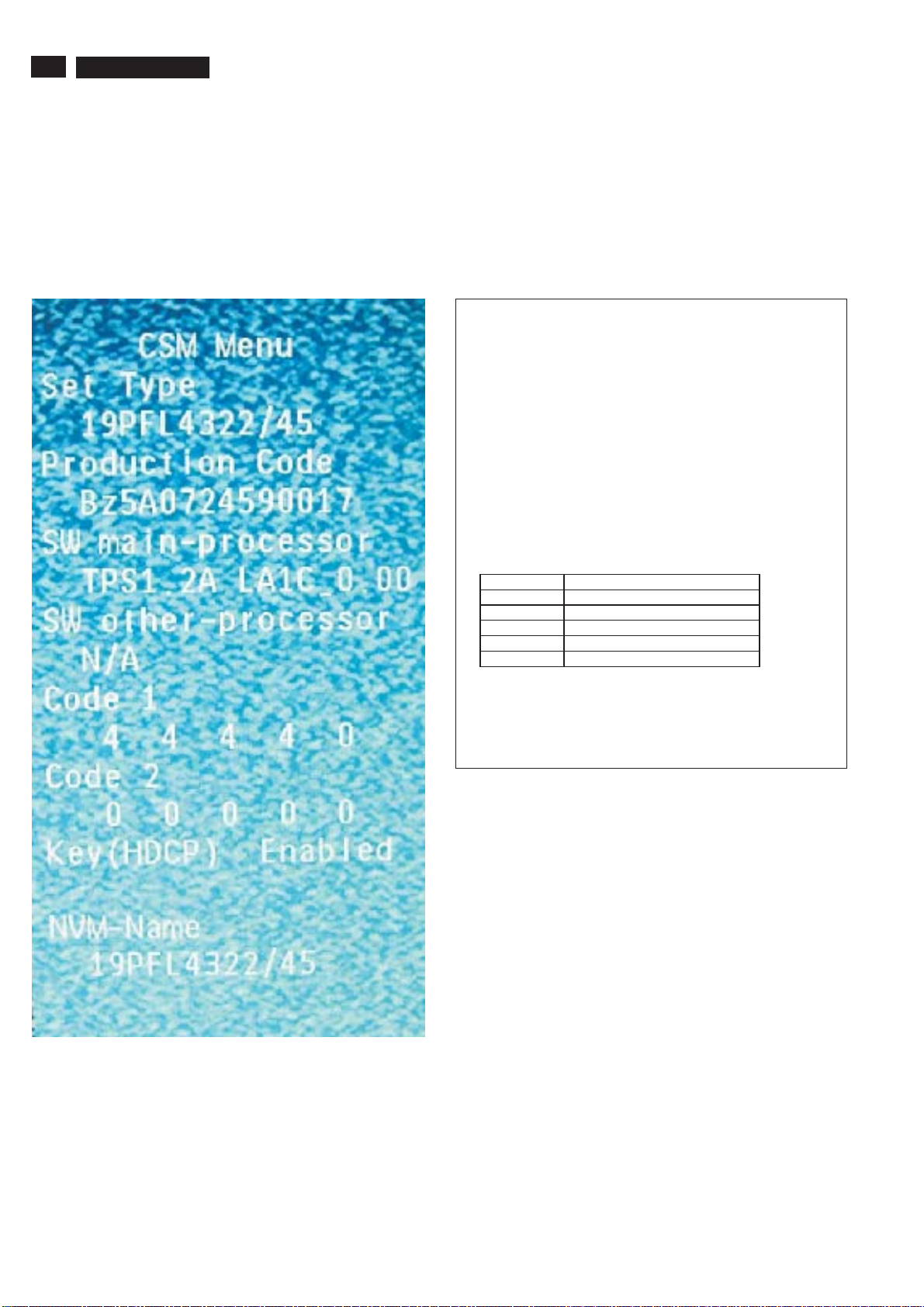
Fig.12
12
TPS 1.0L LA
5. Service Modes, Error Codes and Fault Finding
5. Service Modes, Error Codes and Fault Finding
index of this chapter:
5.1 CSM
5.2 Factory Mode
5.
3 Repair Flow Chart
5.1 CSM
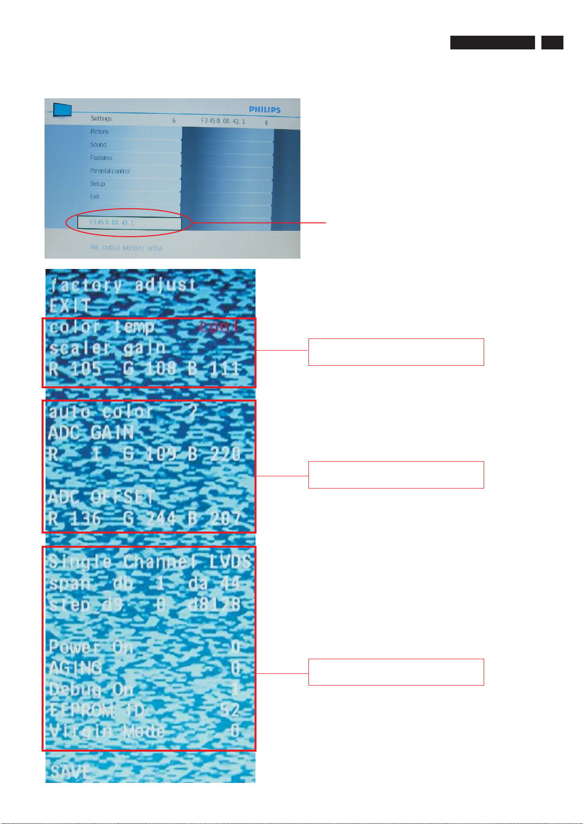
It can display CSM windows message when press 1-2 3-6 5-4 on the button (RC) remote control in normal operation mode.
The following information is displayed on screen:
Set type:
Model type would be displayed on this item. 19PFL4322/45
Production code:
S/N would be displayed on this item.
SW main-processor:
TPS1.2A LA1C_ (current version)
SW other-processor:
N/A
Code 1:
5 last logged errors.
Code 2:
5 first logged errors.
Error code Event
0x01 Audio decoder error
0x02 IIC bus error
0x03 Tuner error
0x04 NVRAM error
0x05 Scaler chip error
Key (HDCP):
HDCP key valid or invalid status would be displayed on this item.
NVM-Name:
Same as set type
5. Service Modes, Error Codes and Fault Finding
5.2 Factory Mode
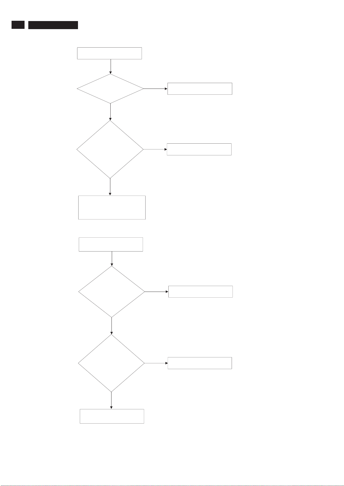
Press "Menu062596 " on remote control then Press "Up " or "Down " button to move cursor to bottom item and then press
"OK " button to enter factory mode.
Factory indicate
TPS 1.0L LA
13
For white balance alignment
For auto color alignment
For design only, please don't adjust it.
14
TPS 1.0L LA
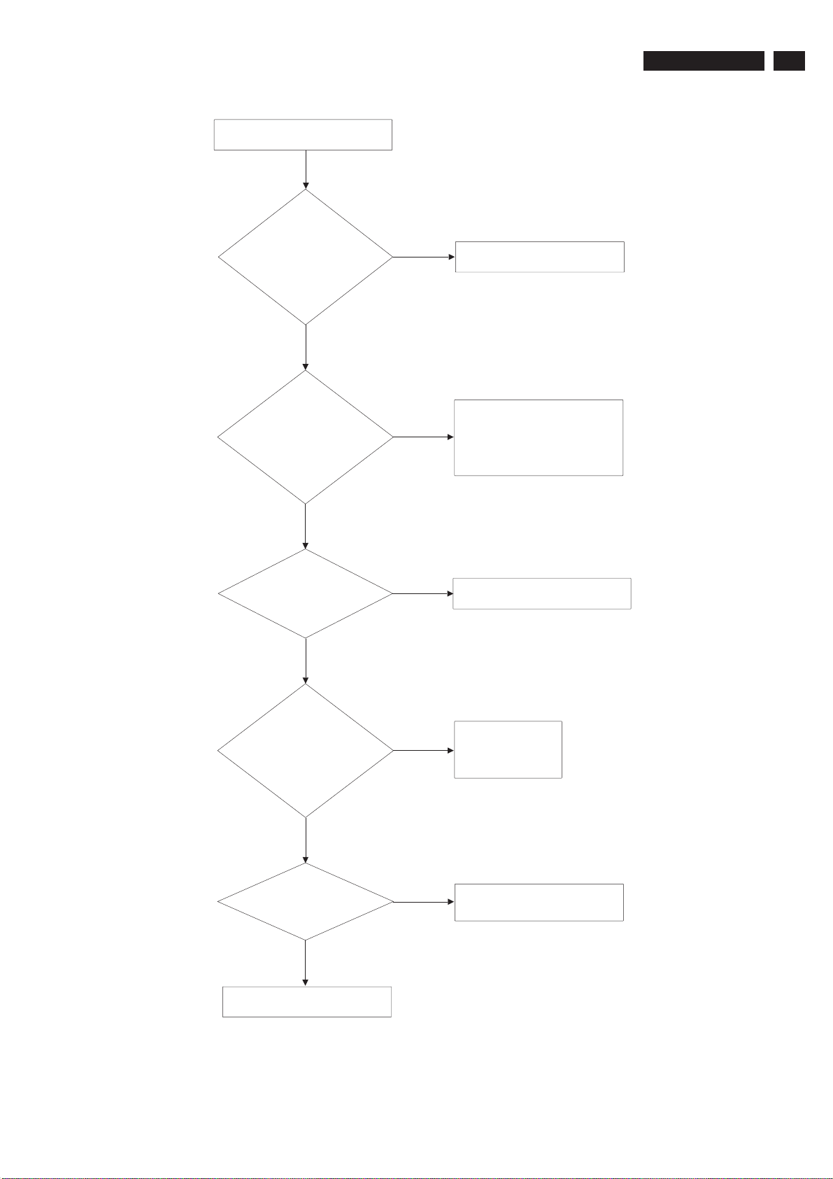
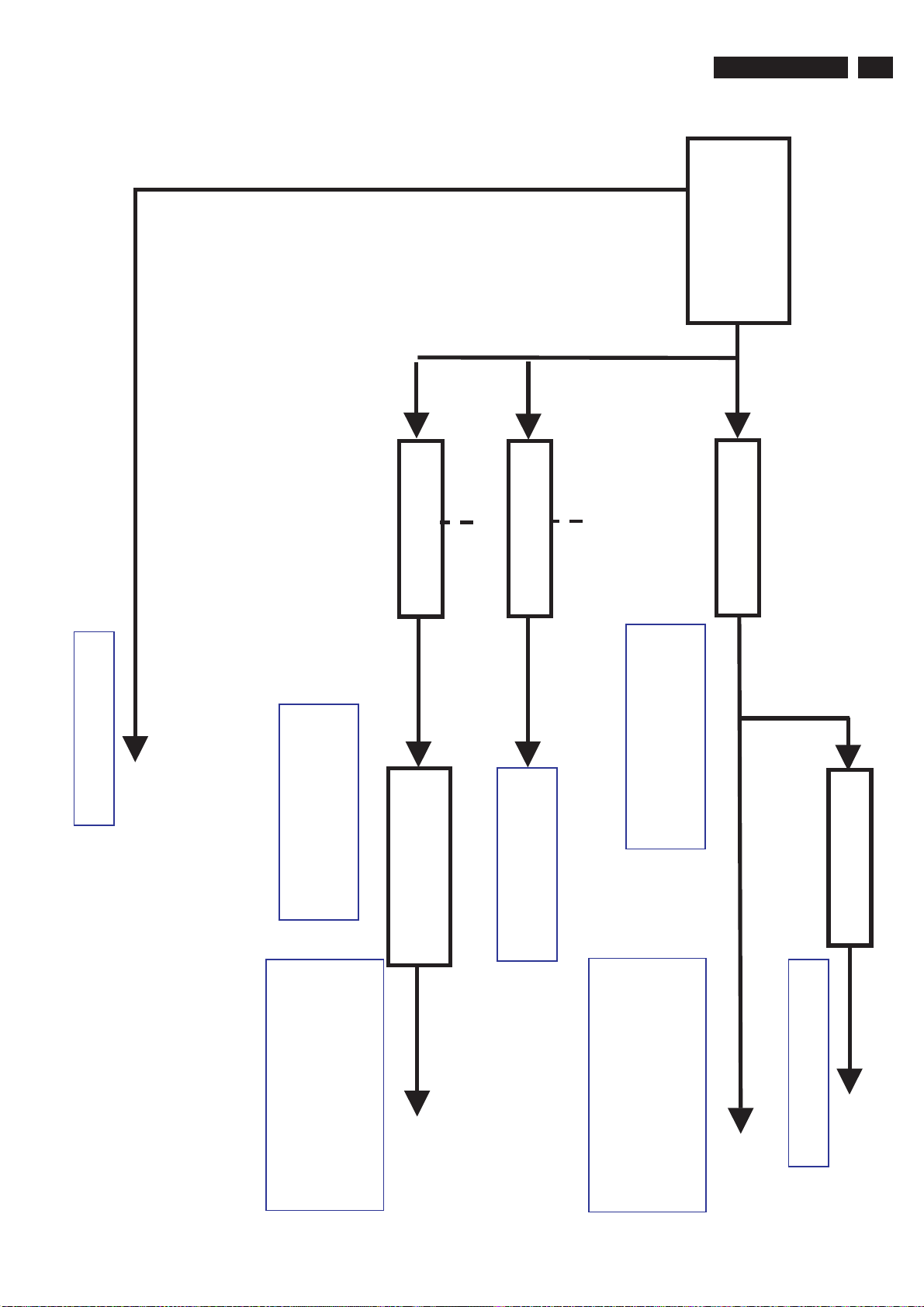
5.3 Repair flow chart
5. Service Modes, Error Codes and Fault Finding
1.No work/LED is off
Check if
power switch is
normal
Yes
Check
IR board CN001
pin1=0V,pin2=3.7V,
pin3=3V,pin4=2.85V
,pin5=5V,pin6
=3.3V
Yes
Check scaler board U102
pin1=14V,pin4=1.22V,
pin7=16V,pin8=5V,
2.No raster/picture too
dim
No
No
Replace Power switch
Check IR board
Check
Inverter board
CN852,pin1=16V,
pin5=0.9V,pin6
=3V
Yes
Check
Inverter board
U811 pin2=5V,Q821
pin=5,6=16V
Yes
Check scaler board
No
No
Check Scaler board
Check U811,Q821
5. Service Modes, Error Codes and Fault Finding
3.No picture/LED is green
Check
scaler board U102
pin1=14V,pin4=1.22V,
pin7=16V,pin8
=5V
Yes
No
Check power
TPS 1.0L LA
15
Check if
working voltage
U152,pin2=3.3V
pin3=5V
Yes
Check if clock
source X350
Yes
Check if
RGB,clk,H/V and
DE signal output 128
bits TTL
No
No
No
Check circuit around
each regulator and
eliminate short and
open situation
Replace X350
Try to replace
flash Rom
EEPROM
Yes
Check
resistors-network
Yes
Replace LVDS cable
No
Replace bad resistorsnetwork

16
TPS 1.0L LA
5. Service Modes, Error Codes and Fault Finding
4.No TV sound
Check if
tuner TU201 pin11
output IF signal
Yes
Check U301
5.No earthphone sound
No
Replace TU201
Check
U760 pin15=3.3V
Yes
Check U760
pin20=HPOUTL
pin6=HPOUTR
Yes
Replace Side AV Board
No
No
Eliminate short and open
situation
Replace U760

5. Service Modes, Error Codes and Fault Finding
6.No remote function
TPS 1.0L LA
17
Tty another
remote control
Yes
Check IR receiver
7.LED and function
key poor
Check circuit around
control board and cable
between control board
and scaler board
No
Replace one good
remote control
8.No HDMI picture
Enter CSM mode
to check item 6
Valid
Check Scaler Board
Invalid
Change U701 writen
HDCP KEY
18
TPS 1.0L LA
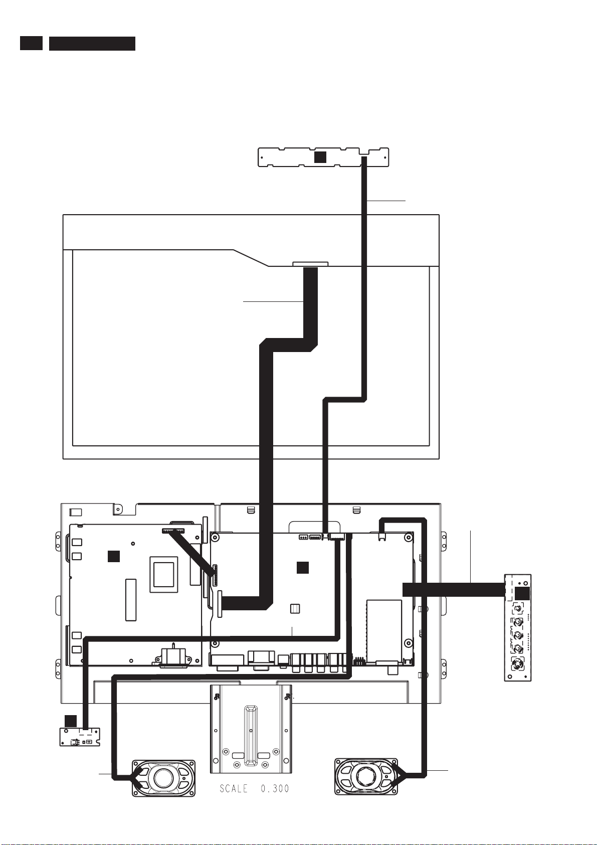
6. Block Diagram
Index of this chapter:
6.1
Wiring Diagram
6.2 Block Diagram
Type: 19PFL4322/45
6. Block Diagram
Wiring Diagram
089T179E30C918
K
CN020
4pin
095T8014 10938 FP
CN0201
I
6pin
095T8013 2982 FP
CN7302
CN7301
3pin
7pin
CN921
11pin
CN6201
2pin
P
CN7201
11pin
30pin
S
CN7501
095T8014 10938 FP
CN6202
2pin
CN7304
10pin
095T8014 10939 FP
CN0304
10pin
SA
095T8013 2979 FP
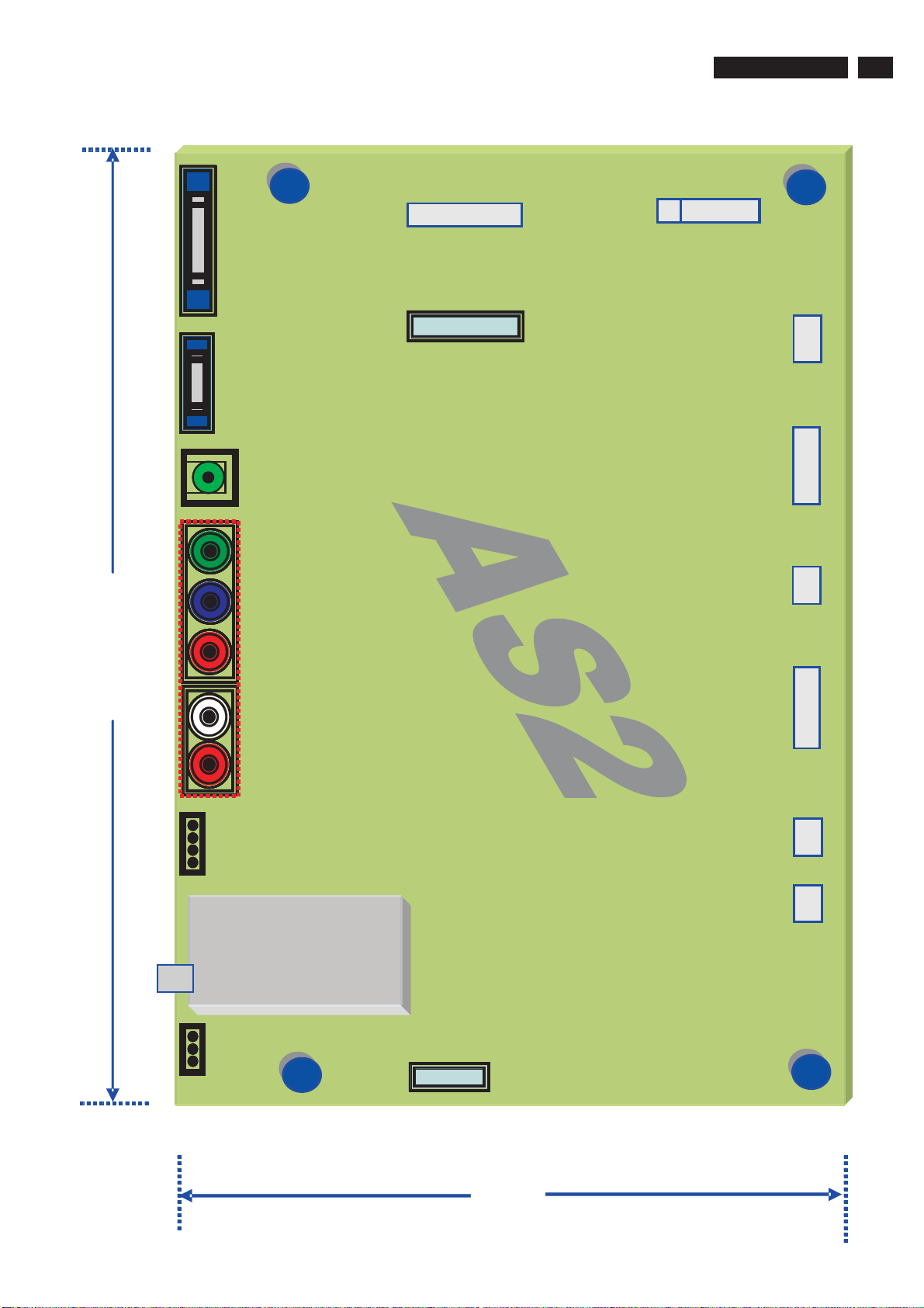
6.2 Block Daigram
6. Block Diagram
F3 - Latam : 19W" Entry
TPS 1.0L LA
19
230 mm
DVI-DDVI-D
DSUBDSUB
PC_AudioPC_Audio
YPbPr
"
20TTL
"
19 LVDS
INVERTER
PWR
PWR I-BD
I-BD
Key BD
Level 1
Level 1
iTV
iTV
ComPair
ComPair
IR BD
Speaker
TUNERTUNER
Side AV
150 mm
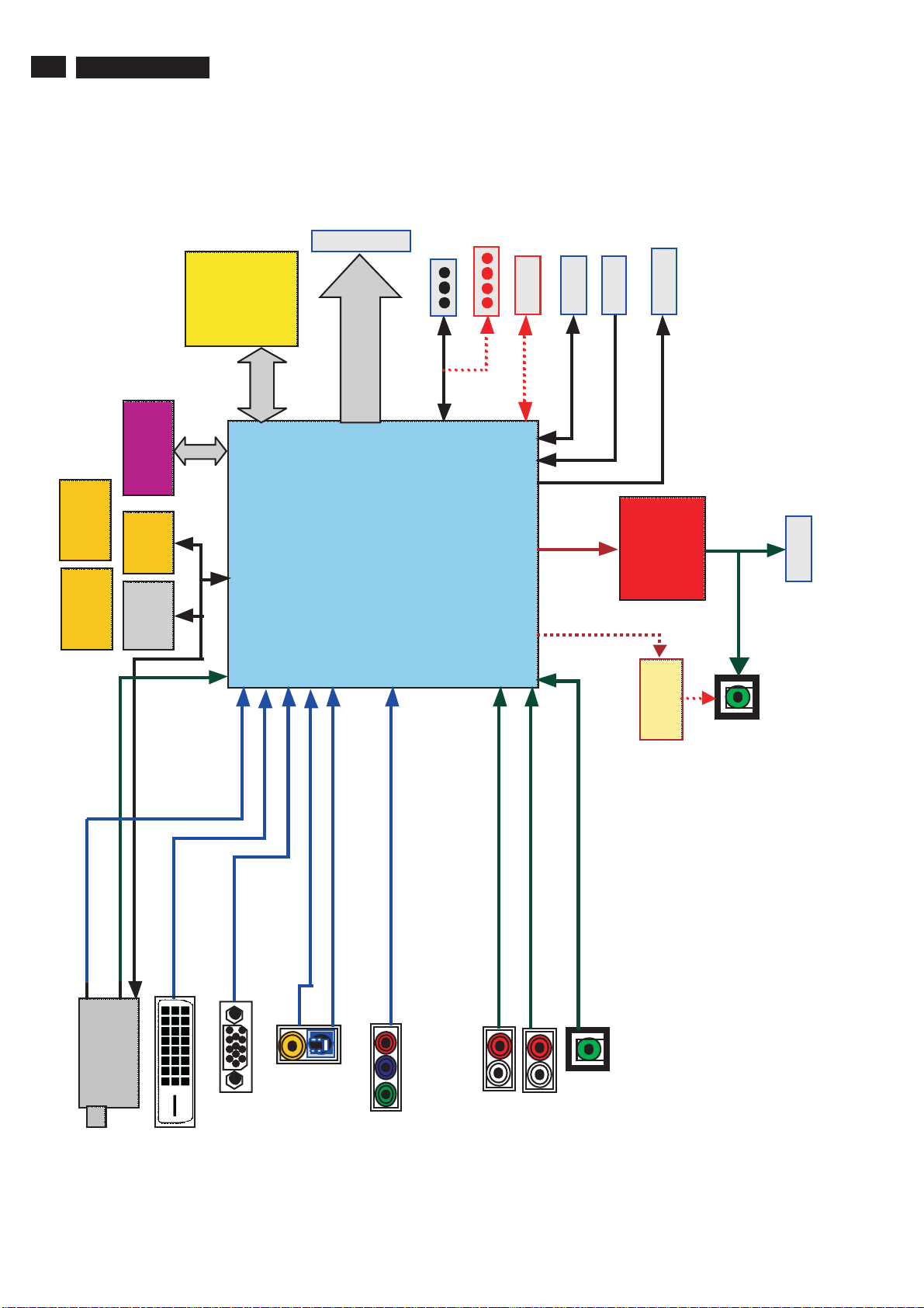
20
TPS 1.0L LA
19W Entry - System Block Diagram"
S-11
6. Block Diagram
LCD Panel
Com Pair
Cloning
(ITV-1)
Video I/F
(ITV-2)
IR Board
Key Board
LIPS control
24C02
S-06
24C02
S-05
S-08
DVI EDID
DSUB EDID
S-08
ROM
SPI Flash
24C16
HDCPK
24C32
NVRAM
SDRAM
SPI
S-07
S-07
I2C
S-09
UART1
TTL/LVDS
MST96885L
S-10
(5P)
S-10
(7P)
S-09
DAC
Line-out
(3P)
S-09
S-13
11P
S-02
AMP
TPA3005D2
1WAMP
TPA6203A
S-13
2x(2P)
(ITV-2)
HP/Bathroom
Speaker
L-R Speaker
CVBS0
SIF0
Tuner
S-03
MM
R1,G1,B1
DVI (CK,RX0,RX1,RX2)
S-06
DVI-D
S-05
D-SUB
Y0,C0
CVBS1
S-Video
CVBS
Y,Pb,Pr (R0,G0,B0)
S-04
S-04
Component-1
AUL1,AUR1
AUL0,AUR0
S-12
CVBSAudio
Component
Audio-1
AUL2,AUR2
S-12
S-12
PCAudio
Remark : Reserve only for ITV function
6. Block Diagram
Power Management
TPS 1.0L LA
LIPS
21
- U6201 ( AUD AMP)
+16V_AUDIO
- U6202 (Bath AMP)
- TU2101 (TUNER)
+16V
U7101 (AIC1596)
PWR_SW
+5V
U7104 (AME8815) or
(AIC1084/5)
+16V
U7105 (AIC1596)
+5V_ITV
- Panel (+5V)
- U7401 (Sync Slicer)
ITV_5V_SW
-
- U1101 (24C02 :D
U5101 (24C02 :DVI
SUB)
-
D)
For IR Board
+16V
U7102 (AIC1596)
+3V3_STBY
U7103 AME8815)
- U4201, 3 (SDRAM)
AVDD_AV, AVDD_MemPLL,,
VDDM
- U4103,5 (HDCP)
- U4202 (Flash ROM)
- U4101 (MST) : AVDD_SIF,
+3V3
- U4102,4 (NVRAM)
- U4101 (MST) : AVVD_DVI,
AVDDA, AVDD_MPLL, VDDP
+3V3_STBY
U4101 (MST) : VDDC
+1V8
22
TPS 1.0L LA
7. Circuit Diagrams and PWB Layouts
ScalerBoardSchematic Daigram-DC-DC POWER
1
2
S-01
A A
B B
C C
+5V_STBY
47K
R7126
R7127
3
R7130
33K(NC)
Q7102
MUN2211J
1
1K
R7131
47K(NC)
ITV_5V_SW7
D D
E E
F F
G G
2
ITV_12V_SW2,7
2
+5V_STBY
2
+16V
R7109
220K
3
Q7107
BC847C
1
R7128
47K(NC)
R7129
1K(NC)
3
Q7105
BC847C(NC)
1
+16V
+16V
C7104
0.1uF
C7125
0.1uF
R7110
100R
2
+16V
3
1
R7114
220K(NC)
Q7108
BC847C(NC)
1
5
3 4
0R
R7103
1
5
3 4
R7116
0R(NC)
+16V
U7101
IN
OUT
ON/OFF
GND FB
AIC1596-33PM5
U7106
IN
OUT
ON/OFF
GND FB
AIC1596-50PM5
C7107
0.1uF(NC)
R7115
100R(NC)
3
2
ZD7101
SSA34-E3
1
R7104 0R
C7106 0.1uF(NC)
R7105
0R(NC)
2
ZD7104
SSA34-E3
1
R7117 0R
C7127 0.1uF(NC)
R7118
0R(NC)
L7101
35uH
L7104
35uH
2
2
FOR iTV (LEVEL 2)
U7102
1
5
3 4
AIC 1596-12PM5(NC)
R7106
0R(NC)
IN
OUT
ON/OFF
GND FB
2
C7105
470uF 25V
C7126
470uF 25V
2
ZD7102
SSA34-E3(NC)
1
R7107 0R(NC)
C7109 0.1uF(NC)
R7108
0R(NC)
L7102
35uH(NC)
4
+3V3_STBY
+5V_ITV
C7108
470uF 25V(NC)
+3V3_STBY
+12V
+5V_ITV
+5V
+16V
5
C7118
0.1uF
R7121
0R05(NC)
1 2
AK
0R05(NC)
1
5
3 4
R7111
0R
D7103
S1D
R7132
R7133
0R05
U7105
IN
OUT
ON/OFF
GND FB
AIC1596-50PM5
C7110
0.1uF
PANEL_PWR7
2
R7113
0R(NC)
PWR_SW7
U7103
AME8815AEGT180Z
1
VIN
C7113
10uF 50V
6
L7103
35uH
2
ZD7103
SSA34-E3
1
R7112 0R
C7120 0.1uF(NC)
2
VOUT
GND
TH
234
2
+5V_STBY
47K
R7124
3
Q7101
MUN2211J
1
C7111
0.1uF
+5V_PANEL+5V_PANEL
56K
R7119
3
Q7104
MUN2211J
1
C7119
470uF 25V
R7125
1K
R7120
75K
2
+1V8
C7114
100uF 10V
1
2
7
R7101
100K
3
Q7106
BC847C
1
1 2
FB7102
220R(NC)
C7122
330N 25V
R7102
390K
R7123
0R05 (NC)
D7104
AK
GF1D(NC)
+5V
+5V_PANEL
1
2
4 5
3
2
1
4 5
3
2
1
C7132
330N 25V
R7122
0R05(NC)
1 2
AK
C7128
0.1uF(NC)
FB7104
220R
Q7103
GS
D
D
D
D
D
D
SI5441DC
8
+5V_STBY
Q7109
GS
6
D
D
7
D
D
8
D
D
SI5441DC
D7102
S1D
C7112
0.1uF
FOR 3V3 PANEL
U7107
AME8815AEGT330Z(NC)
1
C7130
10uF 50V(NC)
+3V3_PANEL+12V
1
FB7103
220R(NC)
2
6
7
8
FB7106
1 2
220R
VIN
C7121
0.1uF
C7133
0.1uF
+5V
C7115
10uF 50V
VOUT
GND
234
TH
U7104
AME8815AEGT330Z
1
VIN
VOUT
GND
234
C7129
0.1uF(NC)
C7123
10uF 50V
TH
C7131
100uF 10V(NC)
PANEL_VCC
C71240.1uF
9
C7116
0.1uF
+3V3_PANEL
+3V3
C7117
100uF 10V
10
C7104 A2
C7105 A4
C7106 B3
C7107 F2
C7108 F4
C7109 F4
C7110 C5
C7111 C6
C7112 C8
C7113 C6
C7114 C7
C7115 C8
C7116 C9
C7117 C9
C7118 A5
C7119 A6
C7120 B6
C7121 F8
C7122 G7
C7123 G8
C7124 G9
C7125 C2
C7126 C4
C7127 C3
C7128 D7
C7129 D8
C7130 D8
C7131 D9
C7132 B7
C7133 A8
D7102 C7
D7103 C5
D7104 D7
FB7102 F7
FB7103 F8
FB7104 F7
FB7106 G8
L7101 A3
L7102 E4
L7103 A6
L7104 C3
Q7101 B6
Q7102 D1
Q7103 F7
Q7104 G6
Q7105 F2
Q7106 B7
Q7107 D2
Q7108 F2
Q7109 A8
R7101 A7
R7102 A7
R7103 B2
R7104 B3
R7105 B3
R7106 F3
R7107 F4
R7108 F3
R7109 C2
R7110 C2
R7111 A5
R7112 A6
R7113 B6
R7114 F2
R7115 F2
R7116 D2
R7117 C3
R7118 C3
R7119 F6
R7120 G7
R7121 C5
R7122 C7
R7123 D7
R7124 B6
R7125 B6
R7126 C1
R7127 D2
R7128 F2
R7129 F2
R7130 F1
R7131 G1
R7132 D5
R7133 D5
U7101 A3
U7102 E3
U7103 C6
U7104 C8
U7105 A5
U7106 C3
U7107 D8
ZD7101 A3
ZD7102 F3
ZD7103 A6
ZD7104 C3
11
H H
1
2
3
4
5
6
7
8
9
10
11
7.Circuit Diagrams and PWB Layouts
TPS 1.0L LA
23
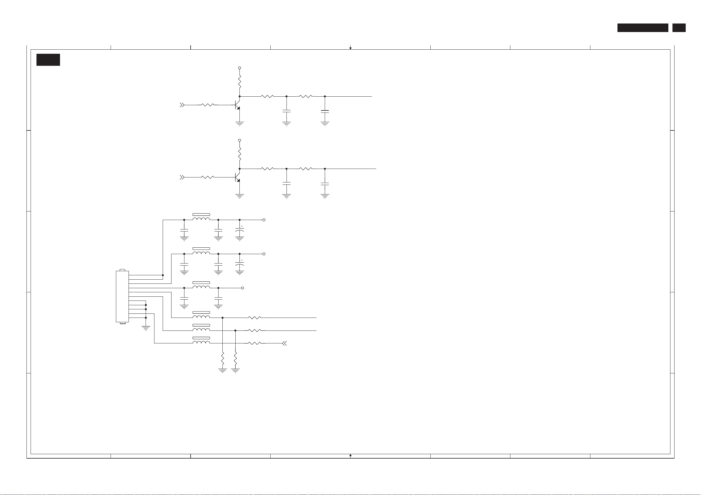
ScalerBoardSchematic Diagram-LIPS &INVERTER I/F
1
S-02
A A
B B
C C
CN7201
1
2
3
4
5
6
7
8
9
10
11
D D
63391 11P 2.0MM
For LIPS/PS
2
BL_ADJ7
BL_EN7
R7204 10K
R7208 10K
FB7201
1 2
120R
C7205
0.1uF
FB7202
1 2
120R
C7208
0.1uF
FB7206
1 2
120R(NC)
C7211
0.1uF(NC)
1 2
FB7203 120R
1 2
FB7204 120R
1 2
FB7205 120R
R7212
0R(NC)
3
2
2
C7206
0.1uF
0.1uF
C7209
C7212
0.1uF(NC)
+5V
R7201
1K
R7202 10K
3
Q7201
BC847C
1
+5V
R7205
1K
R7206 2K2
3
Q7202
BC847C
1
C7213
470uF 25V
C7210
100uF 25V
+12V_ITV
R7209 47R
R7210 47R
R7211 47R
R7213
10K
+16V
+16V_AUDIO
INVERTER_ON_OFF
4
R7203 10R
1U
C7201
R7207 10R
C7203
1U(NC)
BRIGHT_ADJ
ITV_12V_SW 1,7
BRIGHT_ADJ
C7202
0.1uF
INVERTER_ON_OFF
0.1uF
C7204
5
6
7
CN7201 C2
C7201 A4
C7202 A4
C7203 B4
C7204 B4
C7205 C2
C7206 C3
C7208 C2
C7209 C3
C7210 C3
C7211 C2
C7212 C3
C7213 C3
FB7201 B3
FB7202 C3
FB7203 D3
FB7204 D3
FB7205 D3
FB7206 C3
Q7201 A3
Q7202 B3
R7201 A3
R7202 A3
R7203 A4
R7204 A3
R7205 B3
R7206 B3
R7207 B4
R7208 B3
R7209 D3
R7210 D3
R7211 D3
R7212 D3
R7213 D3
8
E E
1
2
3
4
5
6
7
8
24
TPS 1.0L LA
7. Circuit Diagrams and PWB Layouts
ScalerBoardSchematic Daigram- TUNER
1
2
3
4
5
6
7
8
S-03
TU2101 FQ1236/F H-5 TUNER
15
TH1
A A
+5VSCL
SDA
AS_TU
NC
AS_IF
2ND IF SOUND
N.C.
N.C
3
4
2
1
I2C_SCL7,10
B B
C C
I2C_SDA7,10
R2105 47R
R2106 47R
C2108
0.1uF
5
6
R2107
0R(NC)
9
0R
R2103
CVBS
10
11
22uH(NC)
1 2
C2110
1000uF 16V
L2101
FB2102
100R
AF O/P
+5V,IF
13
12
14
C2111
0.1uF
TH2
TH3
TH4
+5V
16
17
18
R2115
10K(NC)
TV_CVBS
R2104
75R 1%
TV_SIF
MONO
1 2
FB2101 30R
C2103
330P(NC)
R2109
2K2(NC)
R2111 10K(NC)
R2112
10K(NC)
22P
C2106
C2101
100P(NC)
C2104
330P(NC)
R2102 47R
R2108 0R
R2110 0R
C2105 0.1uF
C2107 0.1uF
C2109 0.1uF(NC)
C2102 47N
TUNER_CVBS 7
SIFP0 7
SIFM0 7
AUMONO 7
C2101 C5
C2102 B6
C2103 B4
C2104 B5
C2105 B6
C2106 B5
C2107 B6
C2108 C2
C2109 C6
C2110 C3
C2111 C3
FB2101 B5
FB2102 C3
L2101 C3
Q2101 C3
R2101 D4
R2102 B5
R2103 B3
R2104 B4
R2105 B2
R2106 B2
R2107 B2
R2108 B5
R2109 B4
R2110 B5
R2111 C4
R2112 C5
R2113 C3
R2114 C4
R2115 C4
TU2101 A1
3
Q2101
2
BC847C(NC)
R2101
0R(NC)
1
R2114
0R
R2113
0R
D D
E E
1
2
3
4
5
6
7
8
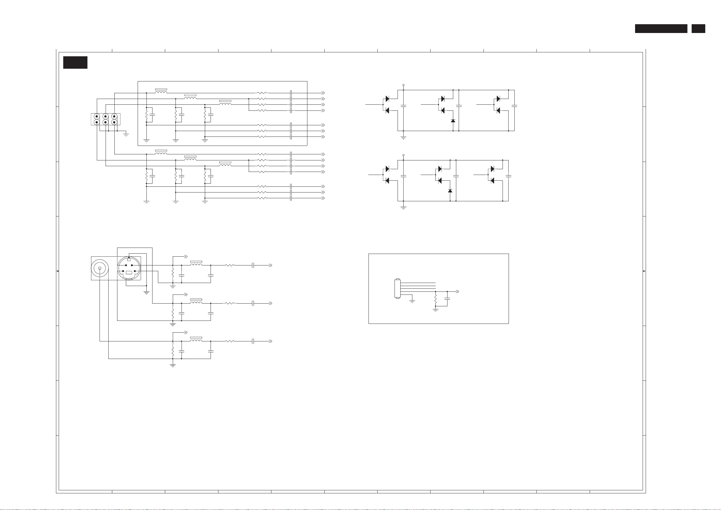
ScalerBoardSchematic Diagram-VIDEO INPUTS
1
2
S-04
7.Circuit Diagrams and PWB Layouts
3
4
5
6
7
8
9
10
11
TPS 1.0L LA
25
A A
R_PR2
G_Y2
B_PB2
32659
1
4
6
7
8
7
PR1
Y1
PB1
1
8
3
5
CN2201
2PJ-AV30-B01
B B
C C
D D
CN2202
5105-840-165-65(NC)
E E
F F
R2206
75R 1%
R2225
75R 1%(NC)
2
4
1 2
FB2208 30R(NC)
C2231
R2226
10P(NC)
75R 1%(NC)
1 2
FB2201 30R
R2207
75R 1%
C2206
10P(NC)
R2201
75R 1%
R2216
75R 1%
R2219
75R 1%
1 2
FB2209 30R(NC)
C2232
R2227
10P(NC)
75R 1%(NC)
1 2
FB2202 30R
R2208
75R 1%
C2207
10P(NC)
SV_Y0_SIDE 9
1 2
FB2205 30R
C2201
330P(NC)
SV_C0_SIDE 9
1 2
FB2206 30R
C2221
330P(NC)
AV_CVBS_SIDE 9
1 2
FB2207 30R
C2224
330P(NC)
1 2
FB2210 30R(NC)
C2233
10P(NC)
1 2
FB2203 30R
C2208
10P(NC)
R2214
47R
C2219
330P(NC)
R2215
47R
C2222
330P(NC)
R2220
47R
C2225
330P(NC)
C2218 47N
C2220 47N
C2226 47N
47R 5%(NC)
R2221
47R 5%(NC)
R2222
47R 5%(NC)
R2223
R2224 470R(NC)
47R 5%(NC)
R2228
47R 5%(NC)
R2229
47R 5%(NC)
R2230
R2202 47R
R2203 47R
R2204 47R
R2205 470R
R2209 47R
R2210 47R
R2211 47R
SV_Y0 7
SV_C0 7
AV_CVBS 7
C2227 47N(NC)
C2228 47N(NC)
C2229 47N(NC)
C2230 1N(NC)
C2234 47N(NC)
C2235 47N(NC)
C2236 47N(NC)
C2202 47N
C2203 47N
C2204 47N
C2205 1N
C2209 47N
C2210 47N
C2211 47N
PR2+
Y2+
PB2+
SOY2
PR2Y2PB2-
PR1+
Y1+
PB1+
SOY1
PR1Y1PB1-
PR2+ 7
Y2+ 7
PB2+ 7
SOY2 7
PR2- 7
Y2- 7
PB2- 7
PR1+ 7
Y1+ 7
PB1+ 7
SOY1 7
PR1- 7
Y1- 7
PB1- 7
D2206
R_PR2 G_Y2 B_PB2
3
BAV99(NC)
D2202
PR1 Y1 PB1
3
BAV99(NC)
+3V3_ESD
2
C2237
0.1uF(NC)
1
+3V3_ESD
2
C2215
0.1uF(NC)
1
For BS Model
CN2203
1
2
3
4
5
63385 5P 2.0mm (NC)
BAV99(NC)
75R 1%(NC)
D2207
3
BAV99(NC)
D2203
3
BAS32L(NC)
R_PR2
G_Y2
B_PB2
R2231
D2205
BAS32L(NC)
D2201
2
1
2
1
2
1
2
AK
1
C2240
0.1uF(NC)
AK
C2216
0.1uF(NC)
FBL2 7
C2238
0.1uF(NC)
BAV99(NC)
D2204
3
BAV99(NC)
D2208
3
CN2201 B1
CN2202 D1
2
C2239
0.1uF(NC)
1
2
C22170.1uF(NC)
1
CN2203 E7
C2201 E3
C2202 B5
C2203 B5
C2204 C5
C2205 C5
C2206 C2
C2207 C3
C2208 C3
C2209 C5
C2210 C5
C2211 C5
C2215 C7
C2216 C8
C2217 C9
C2218 D4
C2219 E3
C2220 E4
C2221 E3
C2222 E3
C2224 F3
C2225 F3
C2226 F4
C2227 A5
C2228 A5
C2229 A5
C2230 B5
C2231 B2
C2232 B3
C2233 B3
C2234 B5
C2235 B5
C2236 B5
C2237 A7
C2238 A8
C2239 A9
C2240 E8
D2201 C8
D2202 C6
D2203 C7
D2204 C8
D2205 B8
D2206 A6
D2207 A8
D2208 A9
FB2201 B2
FB2202 B3
FB2203 B3
FB2205 D3
FB2206 E3
FB2207 F3
FB2208 A2
FB2209 A3
FB2210 A3
R2201 D3
R2202 B4
R2203 B4
R2204 C4
R2205 C4
R2206 C2
R2207 C3
R2208 C3
R2209 C4
R2210 C4
R2211 C4
R2214 D4
R2215 E4
R2216 E3
R2219 F3
R2220 F4
R2221 A4
R2222 A4
R2223 A4
R2224 B4
R2225 B2
R2226 B3
R2227 B3
R2228 B4
R2229 B4
R2230 B4
R2231 E7
G G
H H
1
2
3
4
5
6
7
8
9
10
11
 Loading...