


TV-VCR Combination
Service
Service
14PV120
14PV125
14PV225
/07
/01/07/39/58
/01/07/39/58
Service
14PV422
14PV425
/01/07/39/58
/07
Service Manual
Contents
Chapter
Adjustment Procedure
Sec. 1:
Schematic Diagrams and CBA's
Exploded Views
Mechanical and Electrical Parts Lists
Survey of versions:
/01 PAL-BG, EURO
/07 PAL I, UK/IRELAND
/39 PAL/SECAM-BG+PAL/SECAM-L/L',FRANCE
/58 PAL-BG/DK+SECAM-BG/DK,EAST-EURO
Sec. 2:
Standard Maintenance
Mechanism Alignment Procedures
Disassembly / Assembly of Mechanism
Deck Exploded Views
For technical data reference is made to the Service Manual of
14PV374/01/07/39/58 & 14PV375/01/07/39/58 3103 785 22220.
The present Manual states only the differences.
Safety regulations require that the set be restored to its original
condition and that parts which are identical with those specified
be used.
Published by BK 2003 Video Service Department Printed in Japan c
Copyright reserved Subject to modification GB 3103 785 22230
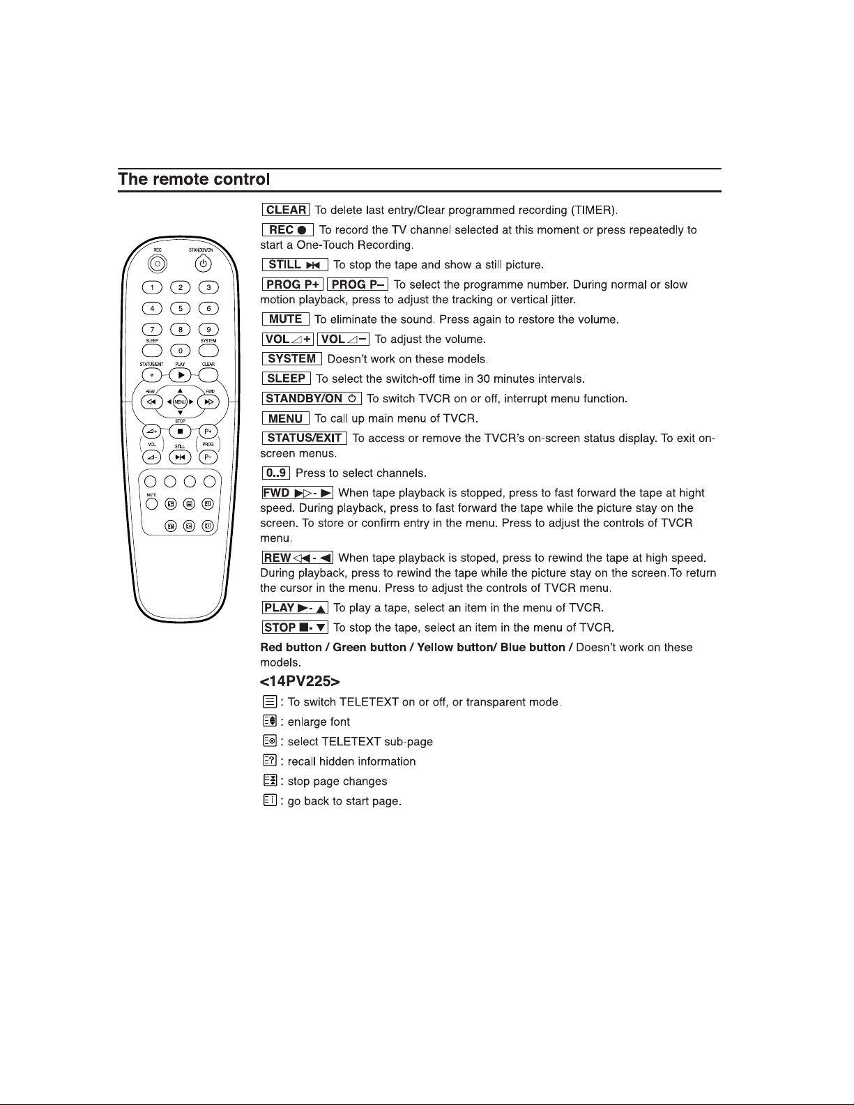
OPERATING CONTROLS AND FUNCTIONS
[ 14PV120/07, 14PV125/ ( 01, 07, 39, 58 ), 14PV225/ ( 01, 07, 39, 58 ),
14PV422/ ( 01, 07, 39, 58 ), 14PV425/07 ]
1-4-3 T6410IB

1-4-4 T6410IB

[
14PV120/07, 14PV125/ (01, 07, 39, 58), 14PV225/ (01, 07, 39, 58),
14PV422/ ( 01, 07, 39, 58 ), 14PV425/07 ]
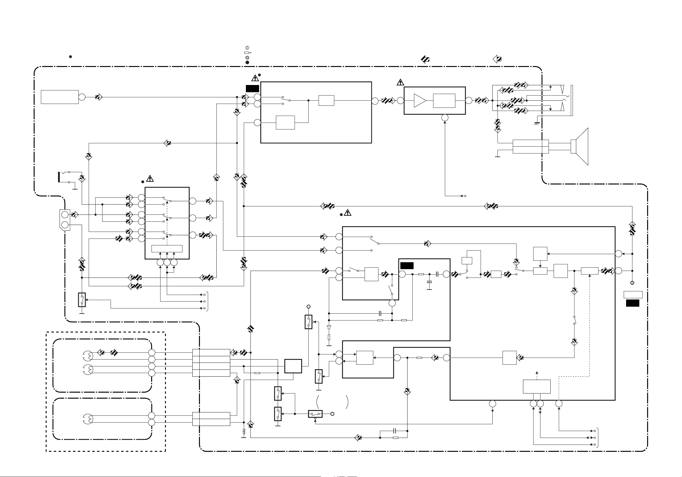
Servo/System Control Block Diagram
(DECK ASSEMBLY)
AC HEAD ASSEMBLY
CL402
CONTROL
HEAD
CYLINDER ASSEMBLY
PG
SENSOR
DRUM
MOTOR
M
LOADING
MOTOR
M
2CTL(+)
1CTL(-)
MAIN CBA
Q202 Q205Q201
ST-SENS.
SENSOR CBA
(ST-SENSOR)
CAPSTAN MOTOR
CAPSTAN
MOTOR
NOTE FOR WIRE CONNECTORS:
1. PREFIX SYMBOL "CN" MEANS CONNECTOR.
(CAN DISCONNECT AND RECONNECT.)
2. PREFIX SYMBOL "CL" MEANS WIRE-SOLDER
HOLES OF THE PCB.
(WIRE IS SOLDERED DIRECTLY.)
END-SENS.
SENSOR CBA
(END-SENSOR)
M
C-CONT
D-PFG
BLOCK DIAGRAMS
TIMER+5V
CN201
1CM+12V
2P-ON+5V(3)
3C-FG
4C-F/R
5
6FG-GND
7LD-CONT
8D-CONT
9
10M-GND
11AL+12V(1)
12VG
D201
S-LED
T-REEL
TEST POINT INFORMATION
AL+5V
RS201
WF3
CTL
SW212
LD-SW
Q204
RESET
CM+12V
P-ON+5V(3)
AL+12V(1)
:INDICATES A TEST POINT WITH A JUMPER WIRE ACROSS A HOLE IN THE PCB.
:USED TO INDICATE A TEST POINT WITH A COMPONENT LEAD ON FOIL SIDE.
:USED TO INDICATE A TEST POINT WITH NO TEST PIN.
:USED TO INDICATE A TEST POINT WITH A TEST PIN.
REMOTE
SENSOR
TP001
AL+5V
+33V
IC201
(SERVO/SYSTEM CONTROL)
KEY-1
REMOTE
14
CTL AMP-OUT
97
95
CTL(+)
CTL(-)
94
LD-SW9
10
ST-SENS.
4
END-SENS.
T-REEL
80
34
RESET
C-FG
87
C-F/R
78
C-CONT
76
81
LD-CONT
77
D-CONT
90
D-PFG
KEY-2
REC LED
REC LED
P-ON-H
P-DOWN-L
I2C-OPEN
SP-MUTE
A-MUTE-H
EXT-L
SCART-H
SCART-MUTE
REC-SAFETY
D-REC-H
C-SYNC
DV-SYNC
V-ENV
C-ROTA
RF-SW
P, T, X
TRICK-H
SECAM-H
SCL
SDA
23
24
67
85
71
72
45
44
20
42
48
29
31
47
74
13
15
18
33
32
Comparison Chart of
Models & Marks
Model Mark
14PV225/07
14PV225/01
14PV225/58
14PV225/39
14PV422/07
SW201 SW205
7
8
D202 REC
D204 STANDBY
SW211
REC
SAFETY
6
KEY SWITCH
SW206 SW210
KEY SWITCH
AL+5V
P-ON-H
P-DOWN-L
IC202
6
SCL
5
SDA
7
CS
I2C-OPEN
SP-MUTE
A-MUTE-H
SCART-H
SCART-MUTE
D-REC-H
C-SYNC
DV-SYNC
V-ENV
C-ROTA
RF-SW
TRICK-H
SECAM-H
(MEMORY)
SCL
SDA
SCL
SDA
EXT-L
SCL
SDA
14PV422/01
14PV422/58
14PV422/39
14PV125/07
14PV125/01
14PV125/58
14PV125/39
14PV125/39
14PV120/07
14PV425/07
FROM/TO POWER
SUPPLY BLOCK
FROM/TO CHROMA
BLOCK
FROM/TO AUDIO
BLOCK
FROM/TO VIDEO
BLOCK
M
N
O
P
Q
R
S
T
U
V
W
X
Y
Z
1-7-15 1-7-16 T6410BLS

Video Block Diagram
" " = SMD
MAIN CBA
TO CHROMA BLOCK
TU001
VIDEO OUT
24
NOTE FOR WIRE CONNECTORS:
1. PREFIX SYMBOL "CN" MEANS CONNECTOR.
(CAN DISCONNECT AND RECONNECT.)
2. PREFIX SYMBOL "CL" MEANS WIRE-SOLDER
HOLES OF THE PCB.
(WIRE IS SOLDERED DIRECTLY.)
C-VIDEO
IC401
(VIDEO/AUDIO SIGNAL PROCESS)
TEST POINT INFORMATION
:INDICATES A TEST POINT WITH A JUMPER WIRE ACROSS A HOLE IN THE PCB.
:USED TO INDICATE A TEST POINT WITH A COMPONENT LEAD ON FOIL SIDE.
:USED TO INDICATE A TEST POINT WITH NO TEST PIN.
:USED TO INDICATE A TEST POINT WITH A TEST PIN.
FROM /TO
SERVO/SYSTEM
CONTROL BLOCK
65
SDA
SCL
REC-VIDEO SIGNAL PB-VIDEO SIGNAL MODE: SP/REC
69684643
7978
Comparison Chart of
Models & Marks
Model Mark
14PV225/07
14PV225/01
14PV225/58
14PV225/39
14PV422/07
14PV422/01
14PV422/58
14PV422/39
14PV125/07
14PV125/01
14PV125/58
14PV125/3914PV125/39
14PV120/07
14PV425/07
M
N
O
P
Q
R
S
T
U
V
W
X
Y
Z
JK701
V-IN
JK703
V-IN
20
V-OUT
19
TO CHROMA
BLOCK
BUFFER
Q703
TU1-VIDEO
VIDEO
Q705
BUFFER
WF5
TP003
V-OUT
Q401
BUFFER
WF4
48
52
54
56
61
63
TUNER1
SCART
PB/EE
TUNER
PB/EE
MUTE
LINE
SCART
LINE
MUTE
BYPASS
AGC
CHARA.
INS.
1/2
FBC
PR
AGC VXO
58 59
Y. DELAY
LUMINANCE
SIGNAL
PROCESS
Y/C
MIX
SERIAL
DECORDER
R
P
CCD 1H DELAY
Y
+
C
CHROMINANCE
SIGNAL
PROCESS
R P R P
2928 44
21
REC FM
AGC
PB-H OUT
SP
HEAD
AMP
D-REC-H
RF-SW/C-ROTA
D-V-SYNC
V-ENV
C-SYNC
96
95
93
94
80
70
62
84
67
WF1
TP002
RF-SW
(DECK ASSEMBLY)
CL401
V(R)
1
V-COM
V(L)
2
3
D-REC-H
RF-SW
C-ROTA
D-V-SYNC
V-ENV
C-SYNC
TRICK-H
SECAM-H
IC471 (PAL/SECAM DECTECOTR)
CYLINDER ASSEMBLY
FROM/TO SERVO/SYSTEM
CONTROL BLOCK
P, T, X
VIDEO (R)
HEAD
VIDEO (L)
HEAD
28
29
17
12
16
14
1
PAL/SECAM
2
DETECTOR
TP010
GND
X401
4.43MHz
WF2
TP008
C-PB
WF6
1-7-17 1-7-18 T6410BLV
Audio Block Diagram
NOTE FOR WIRE CONNECTORS:
1. PREFIX SYMBOL "CN" MEANS CONNECTOR.
(CAN DISCONNECT AND RECONNECT.)
" " = SMD
2. PREFIX SYMBOL "CL" MEANS WIRE-SOLDER
HOLES OF THE PCB.
(WIRE IS SOLDERED DIRECTLY.)
TEST POINT INFORMATION
:INDICATES A TEST POINT WITH A JUMPER WIRE ACROSS A HOLE IN THE PCB.
:USED TO INDICATE A TEST POINT WITH A COMPONENT LEAD ON FOIL SIDE.
:USED TO INDICATE A TEST POINT WITH NO TEST PIN.
:USED TO INDICATE A TEST POINT WITH A TEST PIN.
PB-AUDIO SIGNAL REC-AUDIO SIGNAL Mode : SP/REC
TU001
AUDIO OUT
JK702
A-IN
A-IN
A-OUT
JK703
2
1
21
Q701
IC701 (SW)
1
2
5
3
13
12
SW CTL
1011 9
SCART-MUTE
15
4
14
SCART-H
EXT-L
FROM SERVO
/SYSTEM
CONTROL
BLOCK
WF7
52
53
54
(VIDEO/AUDIO/CHROMA/DEFLECTION/IF)
IC301
TUNER1
LINE
AUDIO
MUTE
+5V
ATT
50
IC401
(AUDIO SIGNAL PROCESS)
TUNER
13
LINE
17
PB-ON
5
6
EQ
AMP
SP/LP-ON
MAIN CBA
IC151 (AMP)
7
WF9
7
OUTPUT
AMP
MUTE
5
98
1
SP-MUTE
(FROM PIN 44 OF IC201)
INV
ATT
CN804
SP
SP-GND 1
R
P
ALC
DET
ALC
2
CL801
LINE
AMP
JK151
HEADPHONE JACK
SP151
SPEAKER
12
MUTE
11
TP007
A-OUT
WF8
(DECK ASSEMBLY)
AUDIO
HEAD
AUDIO
ERASE
HEAD
ACE HEAD ASSEMBLY
FULL
ERASE
HEAD
FE HEAD
REC-ON
71
A-MUTE-H
SDA
SCL
FROM/TO
SERVO/SYSTEM
CONTROL BLOCK
CL402
3 A-PB/REC
4 A-COM
6 AE-H
5 FE-H
CL403
1 FE-H
2 FE-H-GND
Q854
Q855
BIAS
OSC
Q856
Q853(PB=ON)
Q851
Q852(PB=ON)
1
2
SWITCHING
D-REC-OFF
+5V
AUTO
BIAS
3
100
REC
AMP
SERIAL
AUDIO HD-SW
DECODER
CONTROL
16
68 69
1-7-19 1-7-20 T6410BLA

Chroma Block Diagram
NOTE FOR WIRE CONNECTORS:
1. PREFIX SYMBOL "CN" MEANS CONNECTOR.
(CAN DISCONNECT AND RECONNECT.)
" " = SMD
M, N, O, P
IC901 (TELETEXT DECODER)
ADC/
DATA SLICER
DISPLAY
TIMING
I2C I/F
TELETEXT
DECODER
OSC/CLOCK
GENERATOR
TEXT CBA
FROM/TO
SERVO/SYSTEM
CONTROL BLOCK
I2C-OPEN
23
37
36
50
49
35
32
33
34
41
42
(NO CONNECTION)
CN303 is used for
adjustment at factory
2. PREFIX SYMBOL "CL" MEANS WIRE-SOLDER
HOLES OF THE PCB.
(WIRE IS SOLDERED DIRECTLY.)
X901
12MHz
OSC
SCL
SDA
CN901 CN751
5 5Y-SW-OUT
1 1V-SYNC
2 2H-SYNC
4 4SDA
3 3SCL
CN752CN902
2 2OSD-BLK
4 4OSD-B
6 6OSD-G
3 3OSD-R
CN303
INT.MONITOR
I2C-OPEN 2
SDA 4
SCL 5
1
TEST POINT INFORMATION
:INDICATES A TEST POINT WITH A JUMPER WIRE ACROSS A HOLE IN THE PCB.
:USED TO INDICATE A TEST POINT WITH A COMPONENT LEAD ON FOIL SIDE.
:USED TO INDICATE A TEST POINT WITH NO TEST PIN.
:USED TO INDICATE A TEST POINT WITH A TEST PIN.
Q706
Q702
+5V
Q711
Q704
IC301
40
10
11
43
REC VIDEO SIGNAL PB VIDEO SIGNAL
(VIDEO/AUDIO/CHROMA/DEFLECTION/IF)
SERIAL
I/F
INTELLIGENT
MONITORING
SYNC
SEPARATION
CHROMA
TRAP
CHROMA
BPF
LINE/PB
TUNER
LINE/PB
TUNER
CLOCK
CONTROL
CIRCUIT
Mode : SP/REC
MAIN CBA
34
36
X301
4.43MHz
32
Comparison Chart of
Models & Marks
Model Mark
14PV225/07
14PV225/01
14PV225/58
14PV225/39
14PV422/07
14PV422/01
14PV422/58
14PV422/39
14PV125/07
14PV125/01
14PV125/58
14PV125/39
14PV125/39
14PV120/07
14PV425/07
VIDEO
TU1-VIDEO
FROM
VIDEO BLOCK
M
N
O
P
Q
R
S
T
U
V
W
X
Y
Z
SLOW-SW
RAPID-SW
FROM
VIDEO
BLOCK
OSD-B
OSD-G
OSD-R
C-VIDEO
JK703
8
16
7
11
15
IC201
(SYSTEM CONTROL/OSD)
56
C-VIDEO
TEXT-L
OSD-R
OSD-G
OSD-B
OSD-BLK
SLOW-SW-IN
RGB CONT
RAPID-SW-IN
WF18
V-SYNC
WF17
H-SYNC
82
64
63
62
60
68
61
65
59
58
IC703 (SW)
5
3
2
1
12
13
Q710
SW CTL
109 11
15
14
+5V
LUMA
SIGNAL
4
V-SYNC
PROCESS
CIRCUIT
H-SYNC
PROCESS
CIRCUIT
PROCESS
CIRCUIT
PAL
DECODER
BASE BAND
SECAM
DECODER
1H DELAY LINE
17
21
CL301A
27
20
28
OSD MIX/RBG MATRIX/
BLANKING
16
15
14
BLUE2
GREEN1
RED
3
TO
CRT/H.V. BLOCK
CL301B
30
WF10
13
12
WF11
6
7
31
INV
CL302A
FBP3
H-DRIVE2
ACL6
V-RAMP-FB5
V-DRIVE4
FROM/TO
CRT/H.V. BLOCK
CL302B
T6410BLC1-7-21 1-7-22

CRT/H.V. Block Diagram
NOTE FOR WIRE CONNECTORS:
1. PREFIX SYMBOL "CN" MEANS CONNECTOR.
(CAN DISCONNECT AND RECONNECT.)
" " = SMD
2. PREFIX SYMBOL "CL" MEANS WIRE-SOLDER
HOLES OF THE PCB.
(WIRE IS SOLDERED DIRECTLY.)
TEST POINT INFORMATION
:INDICATES A TEST POINT WITH A JUMPER WIRE ACROSS A HOLE IN THE PCB.
:USED TO INDICATE A TEST POINT WITH A COMPONENT LEAD ON FOIL SIDE.
:USED TO INDICATE A TEST POINT WITH NO TEST PIN.
:USED TO INDICATE A TEST POINT WITH A TEST PIN.
REC VIDEO SIGNAL PB VIDEO SIGNAL
Mode : SP/REC
FROM
POWER SUPPLY BLOCK
3
FROM/TO
CHROMA BLOCK
CL302A
3
6
5
4
H.V./POWER SUPPLY CBA
+B
DEF+B
JUNCTION-B
CBA
CN302CL302B
3 3FBP
2 2H-DRIVE
6 6ACL
5 5V-RAMP-FB
4 4V-DRIVE
CN552
Q533
H.DRIVE
WF12
Q551
H.OUTPUT
T552
1
5
3
4
T551 F.B.T.
10
IC551 (V-DEFLECTION CONTROL)
THERMAL
7
AMP
1
6
FOCUS VR
HV
F
S
11
8
7
9
6
SCREEN VR
PROTECTION
PUMP
UP
VCC
2
3
ANODE
FOCUS
SCREEN
HEATER 11
P-ON+160V 33
5
CL501BCL501A
WF13
CN551
L551
DEFLECTION-YOKE
5
4
3
1
VDRIVE
HDRIVE
ANODE
FROM CHROMA
BLOCK CL301A
CN301CL301B
2
4
3
JUNCTION-C
CBA
2 2RED
4 4GREEN
3 3BLUE
CN502
Q501
RED AMP
CRT CBA
Q502
GREEN AMP
JK501
FOCUS
WF15WF14
BLUE AMP
Q503
WF16
CN501
1-7-241-7-23
SCREEN
GND
R
G
B
HEATER
GND
T6410BLCRT
V501
CRT

Power Supply Block Diagram
W601
DG601
DEGAUSSING
COIL
CAUTION !
Fixed voltage power supply circuit is used in this unit.
If Main Fuse (F601) is blown, check to see that all components in the power supply
circuit are not defective before you connect the AC plug to the AC power supply.
Otherwise it may cause some components in the power supply circuit to fail.
SW601
POWER
CN601
F601
T4A/250V
PS602
L601,L602
LINE
FILTER
D601 - D604
BRIDGE
RECTIFIER
HOT COLD
T601
6
4
14
13
11
12
CAUTION
FOR CONTINUED PROTECTION AGAINST FIRE HAZARD,
REPLACE ONLY WITH THE SAME TYPE T4A/250V FUSE.
TP503
+B
TP504
GND
+B
TO
CRT/H.V.
BLOCK
DEF+B
NOTE :
The voltage for parts in hot circuit is measured using
hot GND as a common terminal.
Q206
P-DOWN-L
(TO PIN85 OF IC201)
Q602
SWITCHING
Q603
LIMITER
2
1
4 1
3 2
IC601
ERROR
VOLTAGE DET
10
9
8
Q604
FEED
BACK
Q608
VR601
+B ADJ.
Q606Q605
+5V REG.
+8V REG.
Q607
CN602
AL+33V11
AL+9V8
AL+12V(2)7
AL+12V(1)3
4
P-DOWN-L
AL+5V
5
12
P-ON+8V
6
P-ON-L
CL603BCN603
11
8
7
3
4
5
12
6
JUNCTION-A CBA
11
12
8
7
3
4
5
6
CL603A
11
8
7
3
4
5
12
6
+5V
REG.
+5V
REG.
+5V
REG.
IC301
+5.7V
REG.
Q682
IC681
Q684
Q686
CM+12V
AL+33V
AL+9V
AL+12V(2)
AL+12V(1)
TIMER+5V
AL+5V
P-ON+8V
P-ON-H
(FROM PIN67 OF IC201)
P-ON+5V(2)
P-ON+5V(3)
P-ON+5V(1)
P-ON-ON
3955
1-7-25
H.V./POWER SUPPLY CBA
1-7-26
MAIN CBA
T6410BLP

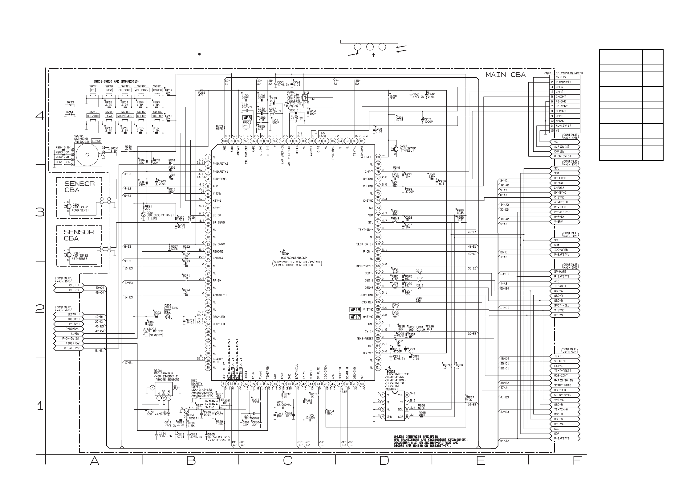
[14PV120/07,14PV125/(01,07,39,57),14PV225/(01,07,39,57),14PV422/
(01,07,39,57),14PV425/07 ]
Main 1/5 Schematic Diagram Parts Location Guide
Ref No. Position Ref No. Position Ref No. Position Ref No. Position
CAPACITORS
C203
C205
C207
C208
C209
C210
C211
C212
C213
C214
C217
C218
C221
C222
C223
C224
C225
C226
C227
C228
C229
C230
C231
C233
C234
C235
C236
C237
C238
C239
C240
C241
C242
C243
C244
C245
C248
C253 B-2 R216 A-4 R264 A-4 RS201 B-1
C254
C255
C256 C-1 R219 B-3 R267 E-1
B-3
B-3
B-1
B-1
C-1
C-1
B-1
B-1
B-1
B-1
C-1
C-1
D-2
D-2
D-2
D-2
D-2
D-2
D-3
D-3
D-3
E-3 RESISTORS
D-4
D-4
D-4
C-4
C-4
C-4
C-4
C-4
C-4
C-4
D-4
D-4
C-4
C-4
B-1
C-4
C-4
CONNECTOR
CN201
DIODES
D201
D202
D204
D205
D206
D210
D211
D212
D213
D214
ICS
IC201
IC202
COIL
L201
TRANSISTORS
Q204
Q205
Q206
R201
R202
R203
R204
R205
R206
R207
R208
R209
R210
R211
R212
R213
R214
R215
R217
R218
F-5
B-3
B-2
B-2
B-1
D-3
D-2
D-2
D-2
A-4
A-4
C-3
D-1
D-2
B-1
D-4
C-4
B-4
B-4
B-3
B-4
B-3
B-3
B-4
B-4
A-4
A-4
A-4
A-4
B-4
B-4
A-4
A-4
B-3
RESISTORS RESISTORS
R220
R221
R222
R223
R224
R226
R227
R228
R229
R230
R231
R232
R233
R234
R235
R236
R237
R238
R239
R240
R241
R242
R243
R244
R248
R249
R250
R254
R255
R256
R257
R258
R259
R260
R261
R262
R263
R265
R266
B-3
B-3
B-3
B-2
B-2
B-1
B-1
B-1
B-1
B-1
C-1
C-1
C-1
C-1
D-2
D-2
D-2
D-2
D-2
D-2
D-3
D-3
D-3
D-3
D-3
D-3
D-3
C-4
C-4
C-4
B-3
B-4
B-4
A-4
A-4
A-4
A-4
D-1
D-1
R268
R269
R270
R271
R272
R273
R274
R275
R276
R277
R278
R279
R280
R281
R282
R287
R288
R289
SWITCH ES
SW201
SW202
SW203
SW204
SW205
SW206
SW207
SW208
SW209
SW210
SW211
SW212
TEST POINT
TP001
CRYSTAL OSCILATORS
X201
X202
MISCELLANEOU S
E-3
E-3
B-1
B-2
B-3
B-2
B-2
D-2
D-2
D-2
D-2
D-2
D-2
C-1
D-2
B-1
E-1
E-1
B-4
A-4
A-4
A-4
A-4
B-4
A-4
A-4
A-4
A-4
B-1
A-4
C-4
C-1
C-1
1-8-43
Main 1/5 Schematic Diagram
Comparison Chart of
MODEL MARK
14PV225/07 M
14PV225/01 N
14PV225/58 O
14PV225/39 P
14PV422/07 Q
14PV422/01 R
14PV422/58 S
14PV422/39 T
14PV125/07 U
14PV125/01 V
14PV125/58 W
14PV125/39 X
14PV120/07 Y
14PV425/07 Z
“ “ = SMD
Voltage indications for PLAY and REC modes on
the Schematic Diagrams are as shown below:
1 2 3
5.0
THE SAME VOLTAGE FOR
BOTH PLAY & REC MODES.
5.0
~
(2.5)
INDICATES THAT THE VOLTAGE
IS NOT CONSISTENT HERE.
PLAY MODE
REC MODE
Models and Marks
1-8-44 1-8-45
T6410SCM1
Main 2/5 Schematic Diagram
“ “ = SMD
Voltage indications for PLAY and REC modes on
the Schematic Diagrams are as shown below:
1 2 3
5.0
THE SAME VOLTAGE FOR
BOTH PLAY & REC MODES.
5.0
~
(2.5)
INDICATES THAT THE VOLTAGE
IS NOT CONSISTENT HERE.
PLAY MODE
REC MODE
1-8-46
1-8-47
T6410SCM2

Main 2/5 Schematic Diagram Parts Location Guide
Ref No. Position Ref No. Position Ref No. Position Ref No. Position
CAPACITORS
C401
C402
C403
C404
C405
C406
C407
C408
C409
C410
C411
C412
C413
C414
C415
C416
C417
C418
C419
C420
C421
C424
C425
C426
C427
C430
C431
C432
C433
C434
C435
C436 H-4 D402 H-4 R422 K-4 TP010 K-1
C438
C440
C441
C442 H-3 L401 K-3 R426 I-4
J-1
J-1
J-2
J-1
J-1
J-2
J-1
J-1
K-2
K-2
K-2
K-2
K-2
K-2
K-3
K-3
K-3
K-3
K-3
K-3
K-3
K-4
J-4
K-4
J-4
H-4
J-4 CL401 G-3
J-4 CL402 G-1
J-4
J-4
I-4
H-4
H-4
H-4
C443
C444
C445
C452
C851
C855
C856
C857
C858
C859
C860
C861
C862
C863
C864
C865
C866
C867
C868
C869
C871
C872
C874
C875
C876
CONNECTORS
CL403
DIODES
D401
IC4 01
COILS
IC
H-3
H-2
H-2
J-4
H-1
H-1
G-1
G-1
H-1
H-1
H-1
H-2
H-1
I-1
I-1
I-1
I-2
I-1
I-1
I-1
I-1
J-1
I-1
I-1
J-1
G-1
K-3
H-2
L402
L403
L852
L854
TRANSISTORS
Q401
Q851
Q852
Q853
Q854
Q855
Q856
Q857
RESISTORS
R401
R402
R405
R406
R407
R408
R409
R410
R411
R412
R413
R414
R415
R416
R417
R418
R420
R423
R424
R425
H-3
H-4
H-1
H-1
J-4
H-1
G-1
G-1
H-1
H-1
H-1
H-3
J-1
J-1
K-2
K-2
K-3
K-4
K-4
J-4
J-4
I-4
I-4
I-4
H-4
H-4 TP002 I-4
H-4
H-3
H-3
K-4
H-4
I-4
RESISTORSCAPACITORS COILS
R851
R852
R853
R854
R856
R857
R858
R859
R860
R861
R862
R863
R864
R865
R866
R867
R869
R870
R871
R874
R876
R877
R878
R879
CRYSTAL OSCILATOR
X401
TEST POINTS
TP00 3
TP00 7
TP00 8
H-1
H-1
H-1
H-1
H-1
G-1
G-1
H-1
H-1
I-1
I-1
H-1
I-1
I-1
I-1
I-1
I-1
I-1
J-2
I-1
I-1
I-1
H-2
H-2
J-2
K-4
I-1
J-1
1-8-48

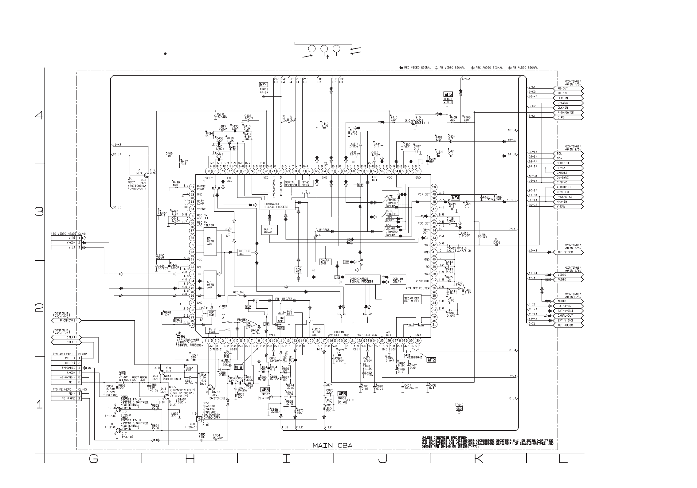
Main 3/5 Schematic Diagram Parts Location Guide
Ref No. Position Ref No. Position Ref No. Position
CAPACITORS
C001
C002
C006
C007
C008
C009
C012
C151
C152
C154
C155
C156
C157
C160
C301
C302
C303
C304
C305
C307
C308
C309
C310
C311
C312
C313
C314
C315
C316
C317
C318
C319
C320
C321
C322
C323
C324
C325
C326
C327
C328
C330 N-2 R153 P-4 TP006 R-4
C331
C332 N-3 R155 N-4
R-4
Q-4
P-4
Q-3
Q-3
R-3
Q-4
O-4
N-4
O-4
P-4
P-4
P-4
P-4
N-1
N-1
N-1
N-1
N-1
O-3
P-2
P-2
P-2
P-2
P-2
P-2
P-2
P-2
P-3
P-3
O-3
P-3
P-3
O-3
O-3
N-3
N-3
N-3
N-3
N-3
N-3
N-2
CAPACITORS RESISTORS
IC
N-2
N-2
P-3
M-3
M-3
P-1
N-2
M-3
N-3
R-1
M-4
M-3
M-4
O-4
O-4
P-1
P-1
P-1
P-3
P-2
O-4
N-1
M-4
Q-4
N-4
N-4
P-2
P-3
N-1
O-4
P-3
P-3
P-3
P-3
M-4
Q-4
P-4
R156
R301
R302
R303
R304
R305
R306
R307
R308
R309
R310
R311
R312
R313
R314
R315
R316
R317
R318
R320
R321
R322
R323
R324
R325
R326
R327
R328
R332
R333
R334
R335
R336
R339
R340
CRYSTAL OSCILATOR
X301 P-3
MISCELLANEOU S
JK151
TU00 1 R-4
TEST POINTS
C333
C334
C336
C338
C339
C340
C341
C344
C350
CONNECTORS
CL301A
CL302A
CN303
CN804
DIODES
D151
D152
D302
D303
D304
D305
D306
IC151
IC301
COILS
J418F3
L001
L151
L152
L302
L303
L304
L305
RESISTORS
R003
R004
R005
R006
R151
R152
R154
N-4
N-1
N-1
N-1
O-1
O-1
O-1
O-1
O-1
O-1
P-1
P-3
O-1
P-2
P-2
P-2
P-2
P-3
P-3
O-3
N-3
N-3
N-3
N-3
N-2
N-2
M-2
N-2
M-3
M-3
M-3
N-3
O-1
O-1
O-1
M-4
1-8-49

Main 3/5 Schematic Diagram
“ “ = SMD
Voltage indications for PLAY and REC modes on
the Schematic Diagrams are as shown below:
1 2 3
5.0
THE SAME VOLTAGE FOR
BOTH PLAY & REC MODES.
5.0
~
(2.5)
INDICATES THAT THE VOLTAGE
IS NOT CONSISTENT HERE.
PLAY MODE
REC MODE
1-8-50 1-8-51
T6410SCM3
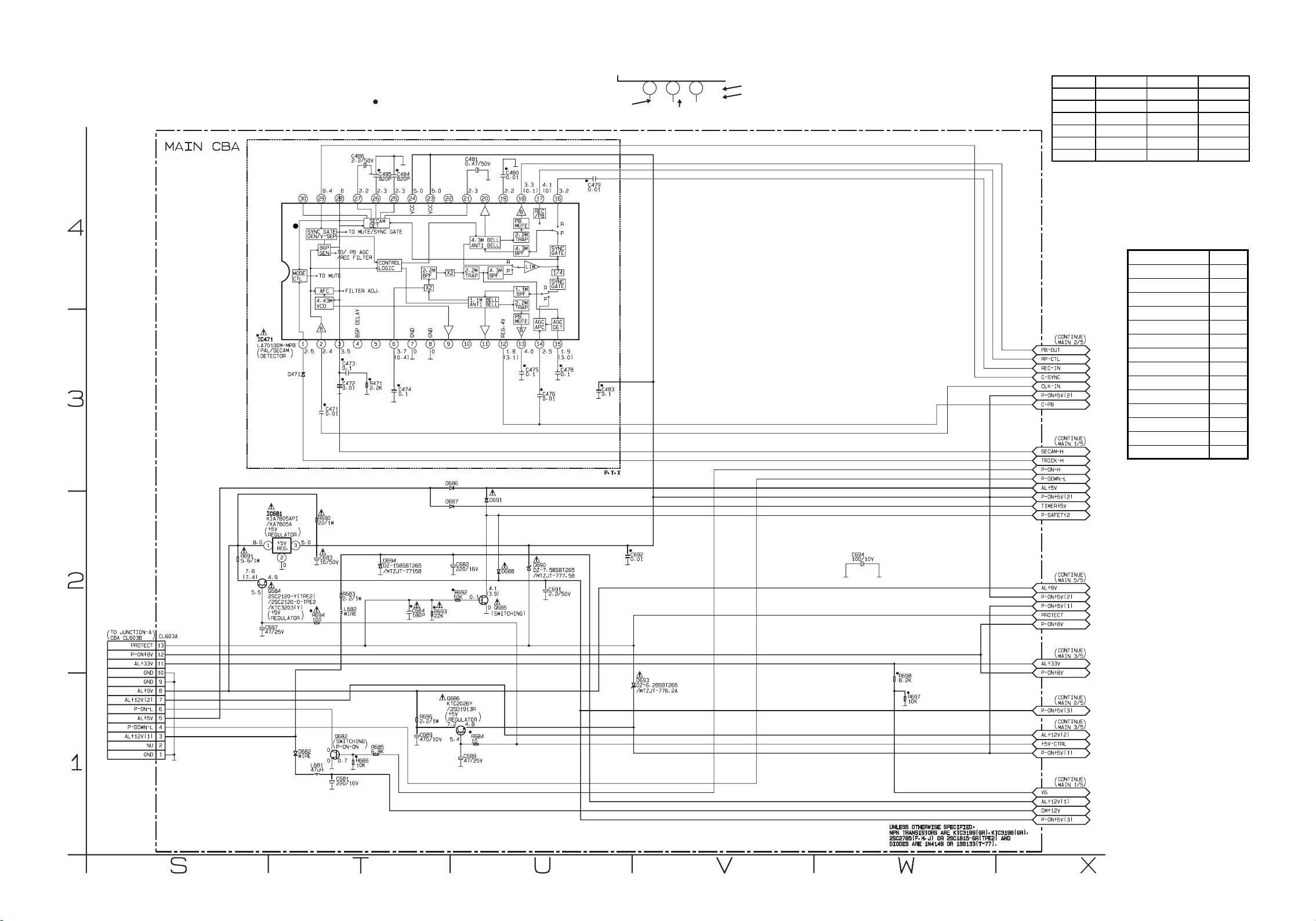
Main 4/5 Schematic Diagram
Ref. No.
IC602
Ref. No.
Q682
Q684
Q685
Q686
03.10
0.1 3.1 0
00.60
123
3.2 0 1.9
07.90
ECB
Comparison Chart of
MODEL MARK
14PV225/07 M
14PV225/01 N
14PV225/58 O
14PV225/39 P
14PV422/07 Q
14PV422/01 R
14PV422/58 S
14PV422/39 T
14PV125/07 U
14PV125/01 V
14PV125/58 W
14PV125/39 X
14PV120/07 Y
14PV425/07 Z
“ “ = SMD
“ “ = SMD
Voltage indications for PLAY and REC modes on
the Schematic Diagrams are as shown below:
1 2 3
5.0
THE SAME VOLTAGE FOR
BOTH PLAY & REC MODES.
5.0
~
(2.5)
INDICATES THAT THE VOLTAGE
IS NOT CONSISTENT HERE.
PLAY MODE
REC MODE
VOLTAGE CHART (Power off mode)
Models and Marks
1-8-52
1-8-53
T6410SCM4

Main 4/5 Schematic Diagram Parts Location Guide
Ref No. Position Ref No. Position
CAPACITORS
C471
C472
C473
C474
C475
C476
C478
C479
C480
C481
C483
C484
C485
C486
C681
C682
C683
C684
C687
C688
C689
C691
C692
C694
CONNECTOR
CL603A
DIODES
D471
D682
D686
D687 U-2 R698 W-1
T-3
T-3
T-3
T-3
U-3
U-3
U-3
U-4
U-4
U-4
U-3
T-4
T-4
T-4
T-1
U-2
T-2
T-2
S-2
U-1
T-1
U-2
U-2
W-2
S-2
T-3
T-1
U-3
DIODES
D688
D690
D691
D693
D694
ICS
IC471
IC681
COILS
L681
L682
TRANSISTORS
Q682
Q684
Q685
Q686
RESISTORS
R471
R681
R683
R684
R685
R686
R690
R691
R692
R693
R694
R696
R697
U-2
U-2
U-2
W-1
T-2
T-3
T-2
T-1
T-2
T-1
S-2
U-2
U-1
T-3
S-1
T-2
U-1
T-1
T-1
T-2
S-2
U-2
T-2
T-2
T-1
W-1
1-8-54

Main 5/5 Schematic Diagram Parts Location Guide
Ref No. Position Ref No. Position
RESISTORSCAPACITORS
ICS
Y-1
BB-2
CC-4
CC-4
AA-4
BB-4
BB-4
CC-4
CC-3
CC-3
CC-3
Z-1
BB-4
BB-1
BB-3
AA-3
Y-4
Y-2
CC-4
CC-3
AA-3
Z-1
BB-4
CC-3
CC-2
AA-2
CC-3
CC-3
BB-3
CC-4
CC-3
BB-4
BB-3
BB-4
AA-2
AA-2
BB-2
BB-3
BB-4
Y-1
Y-1
R705
R707
R709
R710
R711
R712
R714
R723
R724
R725
R726
R727
R728
R729
R730
R731
R732
R733
R734
R735
R736
R737
R738
R739
R740
R741
R742
R743
R744
R745
R746
R747
R748
R749
R750
R751
R752
R753
R754
R755
R756
R757
TEST POINTS
TP009
MISCELLANEOUS
JK701
JK702
C701
C703
C705
C706
C707
C708
C709
C710
C711
C713
C714
C715
C716
C719
C723
C724
CONNECTOR
CN751
CN752
DIODES
D706
D711
D712
D713
D715
D716
IC701
IC703
COILS
L701
L702
TRANSISTORS
Q70 1
Q70 2
Q70 3
Q70 4
Q70 5
Q70 6
Q70 7
Q70 8
Q70 9
Q71 0
Q71 1
RESISTORS
R701
R702
R703 CC-4 JK703 CC-4
R704 CC-4
BB-2
AA-4
CC-4
BB-4
AA-3
CC-4
CC-4
CC-4
CC-4
CC-4
CC-4
CC-3
BB-4
BB-4
BB-4
CC-3
CC-3
CC-3
CC-3
CC-3
CC-3
CC-3
BB-2
CC-2
AA-2
Z-1
AA-2
AA-2
AA-2
AA-2
AA-2
AA-2
AA-2
CC-2
Y-1
Y-2
BB-3
Y-2
BB-3
AA-3
BB-4
BB-4
BB-3
Y-1
Y-1
1-8-55
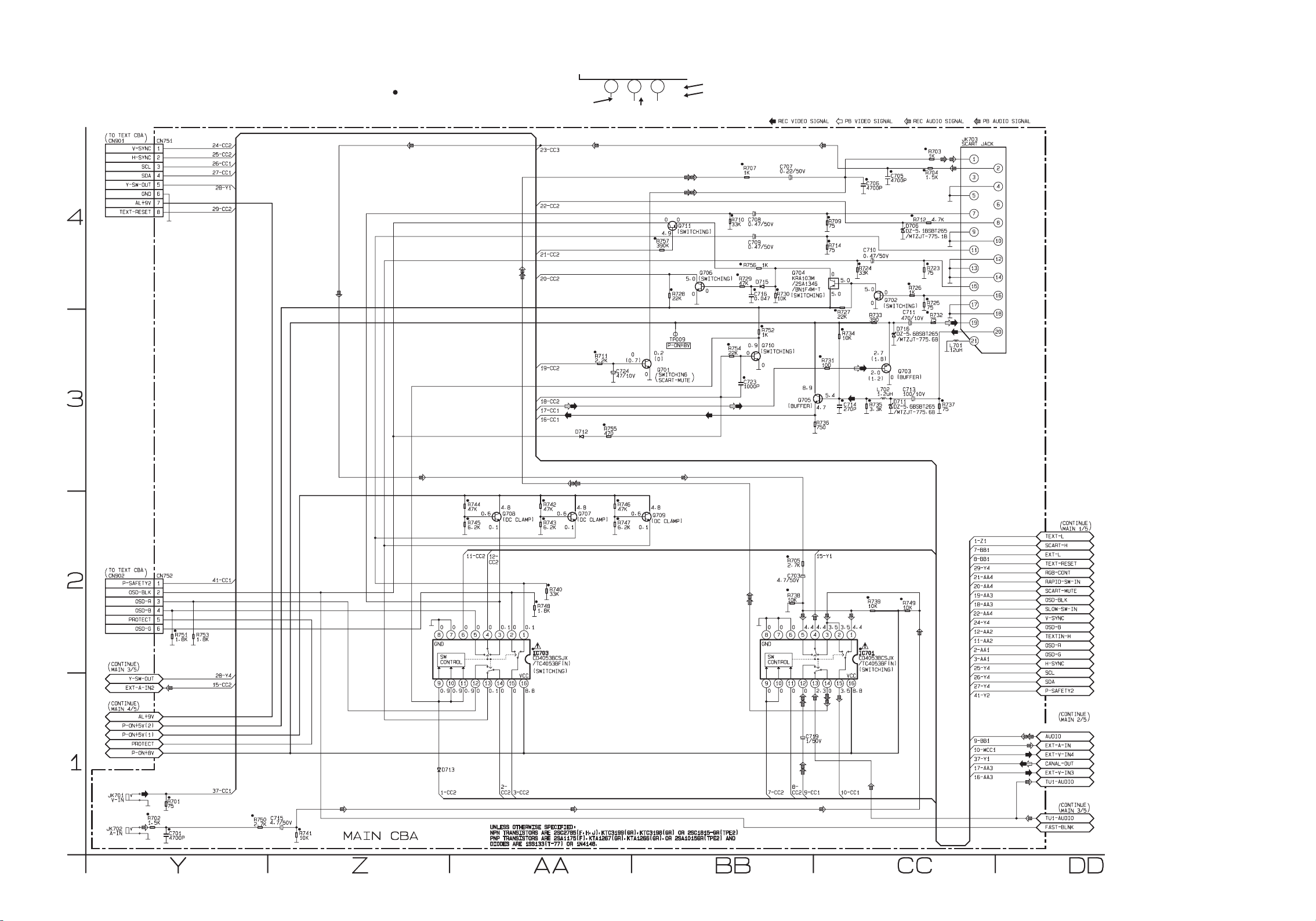
Main 5/5 Schematic Diagram
“ “ = SMD
Voltage indications for PLAY and REC modes on
the Schematic Diagrams are as shown below:
1 2 3
5.0
THE SAME VOLTAGE FOR
BOTH PLAY & REC MODES.
5.0
~
(2.5)
INDICATES THAT THE VOLTAGE
IS NOT CONSISTENT HERE.
PLAY MODE
REC MODE
1-8-56 1-8-57
T6410SCM5

CRT
ANODE
NOTE FOR WIRE CONNECTORS:
1. PREFIX SYMBOL "CN" MEANS CONNECTOR.
(CAN DISCONNECT AND RECONNECT.)
2. PREFIX SYMBOL "CL" MEANS WIRE-SOLDER
HOLES OF THE PCB.
(WIRE IS SOLDERED DIRECTLY.)
CRT CBA
BT6400F01021-B
FOCUS
SCREEN
WIRING DIAGRAM
CN804
SP-GND 1
SP 2
CL801
SP151
SPEAKER
WIRING DIAGRAM FOR SECTION 2 (DECK MECHANISM)
GND
D.Y.
HD
VD
Comparison Chart of
Models & Marks
Model Mark
14PV225/07
14PV225/01
14PV225/58
14PV225/39
14PV422/07
14PV422/01
14PV422/58
14PV422/39
14PV125/07
14PV125/01
14PV125/58
14PV125/3914PV125/39
14PV120/07
14PV425/07
M
N
O
P
Q
R
S
T
U
V
W
X
Y
Z
W601
2
2
CL501B
HEATER1
GND
P-ON+160V3
CL501A
HEATER1
GND
P-ON+160V3
CN551
1
2
3
4
5
CN601
1
2
CN501
T551
FBT
H.V. / POWER SUPPLY CBA
BT6400F01021-A
JK703
1
2
3
4
5
6
7
8
9
10
11
12
13
14
15
16
17
18
19
20
21
CN502
GND 1
RED 2
BLUE 3
GREEN 4
CN552
GND 1
H-DRIVE 2
FBP 3
V-DRIVE 4
V-RAMP-FB 5
ACL 6
P-SAFETY1 7
GND 8
CN602
GND 1
NU 2
AL+12V(1) 3
P-DOWN-L 4
AL+5V 5
P-ON-L 6
AL+12V(2) 7
AL+9V 8
GND 9
GND 10
AL+33V 11
P-ON+8V 12
PROTECT 13
CN301
1
JUNCTION-C CBA
2
BT6400F01011
3
4
SENSOR CBA
(END-SENSOR)
BHB300F01013-A,B
SENSOR CBA
(ST-SENSOR)
BHB300F01013-A,B
1
2
3
JUNCTION-B CBA
4
BT6400F01011
5
6
7
8
CN603
1
2
3
4
5
6
7
JUNCTION-A CBA
8
BT6300F01011
9
10
11
12
13
CL301B
CL302BCN302
CL603B
10
11
12
13
CN201
CL301A
1
2
3
4
1
2
3
4
5
6
7
8
GND1
BLUE2
GREEN3
RED4
(NO CONNECTION)
CN303 IS USED FOR
ADJUSTMENT AT
FACTORY
CL302A
GND1
H-DRIVE2
FBP3
V-DRIVE4
V-RAMP-FB5
ACL6
P-SAFETY17
GND8
CN303
INT.MONITOR
1
I2C-OPEN2
GND3
SDA4
SCL5
MAIN CBA
CL603A
1
2
3
4
5
6
7
8
9
GND1
NU2
AL+12V(1)3
P-DOWN-L4
AL+5V5
P-ON-L6
AL+12V(2)7
AL+9V8
GND9
GND10
AL+33V11
P-ON+8V12
PROTECT13
BT6400F01011
CM+12V/20.5V
P-ON+5V(3)
C-FG
C-F/R
C-CONT
FG-GND
LD-CONT
D-CONT
D-PFG
M-GND
AL+12V(1)
VG
CL401
V(R)
V-COM
V(L)
CL402
CTL(-) 1
CTL(+) 2
A-PB/REC 3
A-COM 4
AE-H/FE-H 5
AE-H 6
CL403
FE-H 1
FE-H GND 2
1
2
3
4
5
6
7
8
9
10
11
12
1
2
3
V-SYNC1
H-SYNC
2
SCL3
SDA
4
Y-SW-OUT5
GND
6
AL+9V7
TEXT-RESET8
P-SAFETY 21
OSD-BLK
2
OSD-R3
OSD-B
4
PROTECT
5
OSD-G
6
CAPSTAN MOTOR
CN901CN751
1
2
3
4
5
6
7
8
CN902CN752
1
2
3
4
5
6
M
TEXT CBA
BT6400F01031
LOADING
MOTOR
CYLINDER ASSEMBLY
PG
SENSOR
DRUM
M
MOTOR
VIDEO
(R)
HEAD
VIDEO
(L)
HEAD
CONTROL HEAD
AUDIO HEAD
AUDIO ERASE
HEAD
AC HEAD ASSEMBLY
FE HEAD
FULL ERASE HEAD
1-10-3
M, N, O, P
1-10-4
T6410WI

IC PIN FUNCTION DESCRIPTIONS
[ 14PV120/07, 14PV125/ ( 01, 07, 39, 58 ), 14PV225/ ( 01, 07, 39, 58 ),
14PV422/ ( 01, 07, 39, 58 ), 14PV425/07 ]
Comparison Chart of Models and Marks
Model Mark
14PV225/07 M
14PV225/01 N
14PV225/58 O
14PV225/39 P
14PV422/07 Q
14PV422/01 R
14PV422/58 S
14PV422/39 T
14PV125/07 U
14PV125/01 V
14PV125/58 W
14PV125/39 X
14PV120/07 Y
14PV425/07 Z
IC 201 (TV/VCR Micro Computer)
“H” ≥ 4.5V, “L” ≤ 1.0V
Pin
Mark
No.
1-
2IN
3IN
4IN
5
6IN
7IN
8IN
9IN
10 IN
11 -
12 -
13
14 IN
IN/
OUT
IN AFC
IN/
OUT
Signal
Name
NU Not Used
P-SAFETY 2
P-SAFETY 1
END-SENS End-Sensor
V-ENV
KEY-1 Key 1 Input
KEY-2 Key 2 Input
LD-SW
ST-SENS Start-Sensor
NU Not Used
NU Not Used
D-V SYNC
REMOTE
Function
Power Sup ply
Failure Detection 2
Power Sup ply
Failure Detection 1
Automatic
Frequency Control
Signal
Video Envelope
Input
Loading Switch
Input
Artificial V-Sync
Output
Remote Signal
Input
Pin
Mark
No.
15 OUT
16 -
17 -
18 OUT
19 -
20
21 -
22 -
23 OUT
24 OUT
25 -
26 -
27 -
28 -
29 IN
30 -
31 IN
M,N,
O,Q,
R,S,
U,V,
32
W,Y,
Z
P, T , X
IN/
OUT
OUT A-MUTE-H
IN SECAM-H
Signal
Name
C-ROTA
NU Not Used
NU Not Used
RF-SW
NU Not Used
NU Not Used
NU Not Used
REC-LED
REC-LED
NU Not Used
NU Not Used
NU Not Used
NU Not Used
SCARTMUTE
NU Not Used
RECSAFETY
NU Not Used
-
Function
Color Phase Rotary
Changeover SIgnal
Video Head
Switching
Pulse
Audio Mute Control
Signal (Mute = “H”)
Recording LED
Control
Signal
Recording LED
Control
Signal
RAPID-Switch Input
Signal from Scart
Jack
Record Protection
Tab Detection
SECAM Mode at
High
1-12-4 T6410PIN

Pin
Mark
No.
M,N,
O,Q,
R,S,
U,V,
W,Y,
33
Z
P, T, X
34 IN
35 IN
36 OUT
37 -
38 IN
39 OUT
40 -
41 OUT
42 OUT
43 IN
44 OUT
45 IN
46 -
47
48 OUT
49 -
50 -
51 -
52 -
53
54 -
55 OUT
56 IN
57 -
58 IN
59 IN
60 OUT
IN/
OUT
OUT TRICK-H
OUT D-REC-H
Signal
Name
NU Not Used
-
RESET
XCIN Sub Clock 32 kHz
XCOUT Sub Clock 32 kHz
TIMER+5V Vcc
XIN Main Clock Input
XOUT Main Clock Output
GND GND
SPOT-KILL
EXT-L
CLKSEL Clock Select (GND)
SP-MUTE
I2C-OPEN
GND GND
SCART-H
OSD-GND OSD GND
NU Not Used
NU Not Used
NU Not Used
- OSDVcc OSDVcc
HLF HLF
TEXT-RESET Tele Text Reset
CV-IN Video Signal Input
GND GND
H-SYNC H-SYNC Input
V-SYNC V-SYNC Input
OSD-BLK
Function
Special Playback =
“H” in SECAM
Mode
System Reset
Signal (Reset=”L”)
Counter-measure
for Spot
External Input or
Playback = Output
Speaker Mute
Signal
White Balance
Adjust Mode
Judgment
Delayed Record
Signal
Switching Signal of
Scart Jack and
RCA Jack
Output for Picture
Cut off
Pin
Mark
No.
61 OUT
62 OUT
63 OUT
64 OUT
65 IN
66 -
67 OUT
68 IN
69 -
70 OUT
71 OUT
72
73 -
74 IN
75 -
76 OUT
77 OUT
78
79 -
80 IN
81 OUT
82 OUT
L
83
84 -
85 OUT
86 -
IN/
OUT
IN/
OUT
OUT C-F/R
Signal
Name
RGB-CONT RGB Control Signal
OSD-B Blue Output
OSD-G Green Output
OSD-R Red Output
RAPIT-SW-IN
NU Not Used
P-ON-H
SLOW-SW-IN
NU Not Used
TEXT-IN-H
SCL
SDA
NU Not Used
C-SYNC C-Sync Input
NU Not Used
C-CONT
D-CONT
NU Not Used
T- R E EL
LD-CONT
TEXT-L
NU Not Used
-
NU Not Used
P-DOWN-L
NU Not Used
Function
RAPID-Switch Input
Signal
Power On Signal at
High
Slow Switch Input
Signal
Tele Text Input
Signal at High
E2PROM/
CHROMA IC Tuner
Communication
Clock
E2PROM/
CHROMA IC Tuner
Communication
Data
Capstan Motor
Control Signal
Drum Motor Control
Signal
Capstan Motor
FWD/REV Control
Signal (FWD=”L”/
REV=”H”)
Take Up Reel
Rotation Signal
Loading Motor
Control Signal
Teletext Control
Signal
Power Voltage
Down Detector
Signal at Low
1-12-5 T6410PIN

Pin
Mark
No.
87 IN
88
89 -
90
91 OUT
92 IN
93
94
95
96 -
97 OUT
98
99
100
IN/
OUT
IN D-PFG
IN/
OUT
IN/
OUT
IN AGC
Signal
Name
C-FG
- AMPVss AMPVss (GND)
NU Not Used
AMP VREFOUT
AMP VREF- INStandard Voltage
- C C Terminal
CTL (-) CTL (-)
CTL (+) CTL (+)
AMPC AMPC
CTL AMPOUT
- AMPVcc AMPVcc
-AVcc
Function
Capstan Motor
Rotation Detection
Pulse
Drum Motor Phase/
Frequency
Generator
Standard Voltage
Output
Input
Control Amp Output
A/D Converter
Power Input/
Standard
Voltage Input
Tuner IF Output
Signal
1-12-6 T6410PIN

LEAD IDENTIFICATIONS
[ 14PV120/07, 14PV125/ ( 01, 07, 39, 58 ), 14PV225/ ( 01, 07, 39, 58 ),
14PV422/ ( 01, 07, 39, 58 ), 14PV425/07 ]
2SK2647
S D G
LA78040A
IN G OUT
KIA7805API
KA7805A
AN7805F
TT2084LS-YB11
TT2138LS-YB11
2SC5884000RF
S: Souce
D: Drain
G: Gate
B C E
E: Emitter
C: Collector
B: Base
KRA103M
2SA1346
2SC1815-GR(TPE2)
2SC3331(T,U)
2SC2120-(O,Y)(TPE2)
KTC3203(Y)
KTA1266(GR)
E C B
PS2561L1-1-VL
PS2561L1-1-VW
LTV817MBF
LTV817MCF
AC
KE
E C B
TC4053BF(N)
CD4053BCSJX
16
PT204-6B-12
MID-32A22
C
E
2SC1627Y-TPE2
2SA950(Y,O)
KTA1271(Y)
2SC2482 TPE6
2SC3468(E,D)-AE
KTC3207
2SA1175(F)
KTA1267(GR)
KTC3198(GR)
9
81
2SD1913(R)
KTC2026Y
B C E
BN1F4M-T
KTC3199(GR)
2SC2785(J,H,F)
2SA1015-GR(TPE2)
M37762MCA-BA2GP
LA71750AM-MTB
80
51
50
IN G OUT
BR24C04F-W
AT24C04N-10SC
M24C04-MN6
BR24C04F
M24C04-WMN6
8
1
5
4
LA4224
8
1
SAA5265
52
1
5
1
8
LA70100M-MPB
30
4
27
1
16
15
26
100
49
64
1
M61209BFP
48
1
33
16
31
30
32
17
1-13-2 T6410LE

h
PRODUCT SAFETY NOTE: Products marked with a h
have special characteristics important to safety.
Before replacing any of these components, read carefully
the product safety notice in this service manual.
Don’t degrade the safety of the product through improper servicing.
NOTES:
C…..±0.25% D…..±0.5% F…..±1%
G…..±2% J…..±5% K…..±10%
M…..±20% N…..±30% Z…..+80/-20%
ELECTRICAL PARTS LIST
Pos.
C001 CHIP CERAMIC CAP.(MELF) F Z 0.01UF/16V 1111111111111
C002 9965 000 14863 ELECTROLYTIC CAP. 47UF/25V M 1111111111111
C006 9965 000 13908 ELECTROLYTIC CAP. 1UF/50V M 1111111111111
C007 CHIP CERAMIC CAP. B K 0.01UF/50V 1111111111111
C008 ELECTROLYTIC CAP. 1UF/50V M 1111111111111
C009 PCB JUMPER D0.6-P5.0 1111111111111
C012 CHIP CERAMIC CAP.(MELF) F Z 0.01UF/16V 1111111111111
C151 ELECTROLYTIC CAP. 330UF/16V M 1111111111111
C152 CERAMIC CAP.(AX) X M 2200PF/16V 1111111111111
C154 ELECTROLYTIC CAP. 470UF/16V M 1111111111111
C155 ELECTROLYTIC CAP. 0.22UF/50V M H7 1111111111111
C156 CHIP CERAMIC CAP. B K 4700PF/50V 1111111111111
C157 ELECTROLYTIC CAP. 10UF/25V M H7 1111111111111
C160 CHIP CERAMIC CAP. CH J 390PF/50V 1111111111111
C203 CHIP CERAMIC CAP.(MELF) F Z 0.01UF/16V 1111111111111
C205 CHIP CERAMIC CAP.(MELF) F Z 0.01UF/16V 1111111111111
C207 ELECTROLYTIC CAP. 1UF/50V M H7 1111111111111
C208 CHIP CERAMIC CAP.(MELF) F Z 0.01UF/16V 1111111111111
C209 CHIP CERAMIC CAP. CH J 22PF/50V 1111111111111
C210 CHIP CERAMIC CAP. CH J 22PF/50V 1111111111111
C211 ELECTROLYTIC CAP. 47UF/6.3V M H7 1111111111111
C212 CHIP CERAMIC CAP.(MELF) F Z 0.01UF/16V 1111111111111
C213 ELECTROLYTIC CAP. 47UF/6.3V M H7 1111111111111
C214 ELECTROLYTIC CAP. 330UF/6.3V M 1111111111111
C217 CHIP CERAMIC CAP. CH D 10PF/50V 1111111111111
C218 CHIP CERAMIC CAP. CH D 10PF/50V 1111111111111
C221 ELECTROLYTIC CAP. 47UF/6.3V M H7 1111111111111
12 NC Description
MAIN CBA
JUNCTION A CBA
JUNCTION B CBA
JUNCTION C CBA
SENSOR CBA
POWER CBA
CRT CBA
TEXT CBA
MMA CBA
Consists of the following
MAIN CBA
CAPACITORS
14PV120/07
14PV125/01
14PV125/07
14PV125/39
14PV125/58
14PV225/01
14PV225/07
14PV225/39
14PV225/58
14PV422/01
1111111111111
1111111111111
1111111111111
1111111111111
1111111111111
1111111111111
1111111111111
1111111
14PV422/07
14PV422/39
14PV422/58
1-14-18

ELECTRICAL PARTS LIST
h
Pos.
C222 CHIP CERAMIC CAP.(MELF) F Z 0.01UF/16V 1111111111111
C223 CHIP CERAMIC CAP.(MELF) Y K 2200PF/35V 1111111111111
C224 CHIP CERAMIC CAP. F Z 0.1UF/50V 1111111111111
C225 CHIP CERAMIC CAP. CH J 560PF/50V 1111111111111
C226 CHIP CERAMIC CAP. F Z 0.1UF/50V 1111111111111
C227 CHIP CERAMIC CAP. CH D 10PF/50V 1111111111111
C228 CHIP CERAMIC CAP. CH D 10PF/50V 1111111111111
C229 CHIP CERAMIC CAP.(MELF) Y K 4700PF/16V 1111111111111
C230 CHIP CERAMIC CAP. F Z 0.1UF/50V 1111111111111
C231 CHIP CERAMIC CAP.(MELF) F Z 0.01UF/16V 1111111111111
C233 CHIP CERAMIC CAP.(MELF) Y K 1000PF/35V 1111111111111
C234 CHIP CERAMIC CAP. B K 0.01UF/50V 1111111111111
C235 ELECTROLYTIC CAP. 47UF/6.3V M H7 1111111111111
C236 CHIP CERAMIC CAP. B K 0.047UF/50V 1111111111111
C237 ELECTROLYTIC CAP. 47UF/6.3V M H7 1111111111111
C238 CHIP CERAMIC CAP. B K 0.047UF/50V 1111111111111
C239 CHIP CERAMIC CAP. CH J 560PF/50V 1111111111111
C240 CHIP CERAMIC CAP.(MELF) Y K 4700PF/16V 1111111111111
C241 ELECTROLYTIC CAP. 22UF/50V M 1111111111111
C242 CHIP CERAMIC CAP.(MELF) F Z 0.01UF/16V 1111111111111
C243 ELECTROLYTIC CAP. 47UF/6.3V M H7 1111111111111
C244 CHIP CERAMIC CAP.(MELF) F Z 0.01UF/16V 1111111111111
C245 ELECTROLYTIC CAP. 47UF/6.3V M H7 1111111111111
C248 ELECTROLYTIC CAP. 47UF/6.3V M H7 1111111111111
C253 CHIP CERAMIC CAP. B K 0.01UF/50V 1111111111111
C256 ELECTROLYTIC CAP. 10UF/25V M H7 1111111111111
C301 CHIP CERAMIC CAP.(MELF) F Z 0.01UF/16V 1111111111111
C302 ELECTROLYTIC CAP. 1000UF/6.3V M 1111111111111
C303 CHIP CERAMIC CAP. B K 0.01UF/50V 1111111111111
C304 CHIP CERAMIC CAP. B K 0.01UF/50V 1111111111111
C305 ELECTROLYTIC CAP. 1UF/50V M 1111111111111
C307 CHIP CERAMIC CAP. F Z 0.1UF/50V 1111111111111
C308 CHIP CERAMIC CAP. F Z 0.1UF/50V 1111111111111
C309 FILM CAP.(P) 0.1UF/50V J 1111111111111
C310 CHIP CERAMIC CAP. F Z 0.1UF/50V 1111111111111
C311 ELECTROLYTIC CAP. 1000UF/6.3V M 1111111111111
C312 CHIP CERAMIC CAP.(MELF) B K 180PF/50V 1111111111111
C313 CHIP CERAMIC CAP. F Z 0.1UF/50V 1111111111111
C314 CHIP CERAMIC CAP. B K 0.01UF/50V 1111111111111
C315 CHIP CERAMIC CAP. F Z 0.1UF/50V 1111111111111
C316 ELECTROLYTIC CAP. 1UF/50V M 1111111111111
C317 CHIP CERAMIC CAP. CH J 150PF/50V 1111111111111
C318 ELECTROLYTIC CAP. 1UF/50V M 1111111111111
C319 ELECTROLYTIC CAP. 1UF/50V M 1111111111111
C320 CHIP CERAMIC CAP. B K 0.01UF/50V 1111111111111
C321 ELECTROLYTIC CAP. 1UF/50V M 1111111111111
C322 ELECTROLYTIC CAP. 470UF/10V M 1111111111111
C323 ELECTROLYTIC CAP. 47UF/25V M 1111111111111
C324 CHIP CERAMIC CAP.(MELF) F Z 0.01UF/16V 1111111111111
C325 MYLAR CAP. 0.22UF/50V J 1111111111111
C326 ELECTROLYTIC CAP. 1UF/50V M 1111111111111
C327 CHIP CERAMIC CAP. B K 0.01UF/50V 1111111111111
C328 MYLAR CAP. 0.22UF/50V J 1111111111111
C330 CHIP CERAMIC CAP.(MELF) F Z 0.01UF/16V 1111111111111
C331 ELECTROLYTIC CAP. 47UF/10V M 1111111111111
C332 CHIP CERAMIC CAP. F Z 0.1UF/50V 1111111111111
C333 CHIP CERAMIC CAP. F Z 0.1UF/50V 1111111111111
C334 CHIP CERAMIC CAP. F Z 0.1UF/50V 1111111111111
C336 ELECTROLYTIC CAP. 47UF/10V M 1111111111111
12 NC Description
14PV120/07
14PV125/01
14PV125/07
14PV125/39
14PV125/58
14PV225/01
14PV225/07
14PV225/39
14PV225/58
14PV422/01
14PV422/07
14PV422/58
14PV422/39
1-14-19

ELECTRICAL PARTS LIST
h
Pos.
C338 CHIP CERAMIC CAP.(MELF) Y K 1000PF/35V 1111111111111
C339 CHIP CERAMIC CAP.(MELF) F Z 0.01UF/16V 1111111111111
C340 CHIP CERAMIC CAP.(MELF) SL J 100PF/50V 1111111111111
C341 CHIP CERAMIC CAP.(MELF) F Z 0.01UF/16V 1111111111111
C344 CHIP CERAMIC CAP.(MELF) Y K 1000PF/35V 1111111111111
C350 ELECTROLYTIC CAP. 220UF/10V M 1111111111111
C401 CHIP CERAMIC CAP. B K 0.01UF/50V 1111111111111
C402 ELECTROLYTIC CAP. 1UF/50V M H7 1111111111111
C403 ELECTROLYTIC CAP. 1UF/50V M H7 1111111111111
C404 ELECTROLYTIC CAP. 100UF/6.3V H7 1111111111111
C405 CHIP CERAMIC CAP. F Z 0.1UF/50V 1111111111111
C406 CHIP CERAMIC CAP. B K 0.047UF/50V 1111111111111
C407 CHIP CERAMIC CAP. B K 0.01UF/50V 1111111111111
C408 CHIP CERAMIC CAP. F Z 0.1UF/50V 1111111111111
C409 CHIP CERAMIC CAP. B K 0.047UF/50V 1111111111111
C410 CHIP CERAMIC CAP. B K 0.01UF/50V 1111111111111
C411 CHIP CERAMIC CAP. B K 0.01UF/50V 1111111111111
C412 ELECTROLYTIC CAP. 1UF/50V M H7 1111111111111
C413 CHIP CERAMIC CAP. B K 0.01UF/50V 1111111111111
C414 CHIP CERAMIC CAP. F Z 0.1UF/50V 1111111111111
C415 CHIP CERAMIC CAP. B K 0.01UF/50V 1111111111111
C416 ELECTROLYTIC CAP. 47UF/6.3V M H7 1111111111111
C417 ELECTROLYTIC CAP. 1UF/50V M H7 1111111111111
C418 ELECTROLYTIC CAP. 1UF/50V M H7 1111111111111
C419 CHIP CERAMIC CAP. F Z 0.1UF/50V 1111111111111
C420 CHIP CERAMIC CAP. F Z 0.1UF/50V 1111111111111
C421 ELECTROLYTIC CAP. 10UF/25V M H7 1111111111111
C424 CHIP CERAMIC CAP. F Z 0.1UF/50V 1111111111111
C425 CHIP CERAMIC CAP. CH J 68PF/50V 1111111111111
C426 CHIP CERAMIC CAP. F Z 0.1UF/50V 1111111111111
C427 CHIP CERAMIC CAP. F Z 0.1UF/50V 1111111111111
C430 ELECTROLYTIC CAP. 47UF/25V M 1111111111111
C431 CHIP CERAMIC CAP. F Z 0.1UF/50V 1111111111111
C432 ELECTROLYTIC CAP. 1UF/50V M H7 1111111111111
C433 ELECTROLYTIC CAP. 10UF/25V M H7 1111111111111
C434 ELECTROLYTIC CAP. 22UF/16V M H7 1111111111111
C435 ELECTROLYTIC CAP. 1UF/50V M H7 1111111111111
C436 CHIP CERAMIC CAP. CH J 120PF/50V 1111111111111
C438 CHIP CERAMIC CAP. CH J 220PF/50V 1111111111111
C440 ELECTROLYTIC CAP. 1UF/50V M H7 1111111111111
C441 CHIP CERAMIC CAP. F Z 0.1UF/50V 1111111111111
C442 CHIP CERAMIC CAP. F Z 0.1UF/50V 1111111111111
C443 ELECTROLYTIC CAP. 1UF/50V M H7 1111111111111
C444 CHIP CERAMIC CAP. B K 1000PF/50V 1111111111111
C445 ELECTROLYTIC CAP. 10UF/25V M H7 1111111111111
C452 CHIP CERAMIC CAP. CH J 68PF/50V 1111111111111
C471 CHIP CERAMIC CAP. B K 0.01UF/50V 1 1 1
C472 CHIP CERAMIC CAP. B K 0.01UF/50V 1 1 1
C473 CHIP CERAMIC CAP. F Z 0.1UF/50V 1 1 1
C474 CHIP CERAMIC CAP. F Z 0.1UF/50V 1 1 1
C475 CHIP CERAMIC CAP. F Z 0.1UF/50V 1 1 1
C476 CHIP CERAMIC CAP. B K 0.01UF/50V 1 1 1
C478 CHIP CERAMIC CAP. F Z 0.1UF/50V 1 1 1
C479 CHIP CERAMIC CAP. B K 0.01UF/50V 1 1 1
C480 CHIP CERAMIC CAP. B K 0.01UF/50V 1 1 1
C481 ELECTROLYTIC CAP. 0.47UF/50V M H7 1 1 1
C483 CHIP CERAMIC CAP. F Z 0.1UF/50V 1 1 1
C484 CHIP CERAMIC CAP. CH J 820PF/50V 1 1 1
C485 CHIP CERAMIC CAP. CH J 820PF/50V 1 1 1
12 NC Description
14PV120/07
14PV125/01
14PV125/07
14PV125/39
14PV125/58
14PV225/01
14PV225/07
14PV225/39
14PV225/58
14PV422/01
14PV422/07
14PV422/58
14PV422/39
1-14-20

ELECTRICAL PARTS LIST
h
Pos.
C486 ELECTROLYTIC CAP. 2.2UF/50V M H7 1 1 1
C681 ELECTROLYTIC CAP. 220UF/16V M 1111111111111
C682 ELECTROLYTIC CAP. 220UF/16V M 1111111111111
C683 ELECTROLYTIC CAP. 10UF/50V M 1111111111111
C684 CHIP CERAMIC CAP.(MELF) SL J 100PF/50V 1111111111111
C687 ELECTROLYTIC CAP. 47UF/25V M 1111111111111
C688 ELECTROLYTIC CAP. 47UF/25V M 1111111111111
C689 ELECTROLYTIC CAP. 470UF/10V M 1111111111111
C691 ELECTROLYTIC CAP. 2.2UF/50V M 1111111111111
C692 CHIP CERAMIC CAP.(MELF) F Z 0.01UF/16V 1111111111111
C694 ELECTROLYTIC CAP. 100UF/10V M 1111111111111
C701 CHIP CERAMIC CAP.(MELF) Y K 4700PF/16V 1111111111111
C703 ELECTROLYTIC CAP. 4.7UF/50V M 1111111111111
C705 CHIP CERAMIC CAP.(MELF) Y K 4700PF/16V 1111111111111
C706 CHIP CERAMIC CAP.(MELF) Y K 6800PF/16V 1111111111111
C707 ELECTROLYTIC CAP. 0.22UF/50V M 1111111111111
C708 ELECTROLYTIC CAP. 0.47UF/50V M 1111111111111
C709 ELECTROLYTIC CAP. 0.47UF/50V M 1111111111111
C710 ELECTROLYTIC CAP. 0.47UF/50V M 1111111111111
C711 ELECTROLYTIC CAP. 470UF/10V M 1111111111111
C713 ELECTROLYTIC CAP. 100UF/10V M 1111111111111
C714 CHIP CERAMIC CAP. CH J 270PF/50V 1111111111111
C715 ELECTROLYTIC CAP. 4.7UF/50V M 1111111111111
C716 CHIP CERAMIC CAP. B K 0.047UF/50V 1111111111111
C719 ELECTROLYTIC CAP. 1UF/50V M 1111111111111
C723 CHIP CERAMIC CAP.(MELF) Y K 1000PF/35V 1111111111111
C724 ELECTROLYTIC CAP. 47UF/10V M 1111111111111
C851 ELECTROLYTIC CAP. 47UF/6.3V M H7 1111111111111
C855 ELECTROLYTIC CAP. 220UF/6.3V M H7 1111111111111
C856 CERAMIC CAP. B K 470PF/100V 1111111111111
C857 FILM CAP.(P) 0.018UF/100V J 1111111111111
C858 CHIP CERAMIC CAP. B K 2200PF/50V 1111111111111
C859 CHIP CERAMIC CAP.(MELF) SL J 33PF/50V 1111111111111
C860 PCB JUMPER D0.6-P5.0 1111111111111
C861 CERAMIC CAP.(AX) X M 1800PF/16V 1111111111111
C862 ELECTROLYTIC CAP. 10UF/25V M H7 1111111111111
C863 CHIP CERAMIC CAP. B K 0.01UF/50V 1111111111111
C864 CHIP CERAMIC CAP. F Z 0.1UF/50V 1111111111111
C865 CHIP CERAMIC CAP. B K 0.022UF/50V 1111111111111
C866 ELECTROLYTIC CAP. 33UF/10V H7 1111111111111
C867 ELECTROLYTIC CAP. 4.7UF/50V M H7 1111111111111
C868 CHIP CERAMIC CAP.(MELF) Y K 4700PF/16V 1111111111111
C869 CHIP CERAMIC CAP. F Z 0.1UF/50V 1111111111111
C871 CHIP CERAMIC CAP.(MELF) B K 150PF/50V 1111111111111
C872 ELECTROLYTIC CAP. 1UF/50V M H7 1111111111111
C874 CHIP CERAMIC CAP. F Z 0.1UF/50V 1111111111111
C875 CHIP CERAMIC CAP. CH J 220PF/50V 1111111111111
C876 CHIP CERAMIC CAP. B K 0.01UF/50V 1111111111111
1005 3143 027 10191 TUN IF V+U PLL IEC BGDKI 03 1 1 1 1 1 1 1 1 1 1
1005 3143 027 10201 TUN IF V+U PLL IEC BGDKIL 03 1 1 1
5000 3143 021 00011 COI DEGAUS FUNAI 1111111111111
8000 3143 021 00031 EARTH CABLE 1111111111111
8016 2422 070 98211 MAINSCORD EUR 2A5 1M7 JH BK B 1 1 1 1 1 1 1 1 1
8016 2422 070 98218 MAINSCORD UK 5A 1M8 BK B 1 1 1 1
CL604 9965 000 18088 WIRE ASSEMBLY 1P/45 1111111111111
CN201 9965 000 13840 FFC/FPC CONNECTOR, 12P 1111111111111
CN301 9965 000 05261 CONNECTOR 4P TUC-P04X-B1 1111111111111
12 NC Description
MISCELLANEOUS
CONNECTORS
14PV120/07
14PV125/01
14PV125/07
14PV125/39
14PV125/58
14PV225/01
14PV225/07
14PV225/39
14PV225/58
14PV422/01
14PV422/07
14PV422/58
14PV422/39
1-14-21

ELECTRICAL PARTS LIST
h
Pos.
CN302 9965 000 13916 CONNECTOR, 8P TUC-P08X-B1 1111111111111
CN303 9965 000 13841 CONNECTOR BASE, 5P TUC-P05P-B1 1111111111111
CN603 9965 000 18089 CONNECTOR 13P TUC-P13X-B1 1111111111111
CN751 9965 000 13842 CONNECTOR BASE, 8P TUC-P08P-B1 1111111111111
CN752 9965 000 13843 CONNECTOR BASE, 6P TUC-P06P-B1 1111111111111
CN804 9965 000 13844 STRAIGHT CONNECTOR BASE 1111111111111
D151 9965 000 13848 ZENER DIODE MTZJT-777.5B 1111111111111
D152 4822 130 32778 SWITCHING DIODE 1SS133(T-77) 1111111111111
D201 9965 000 05250 LED SIR-563ST3F P 1111111111111
D202 9965 000 13846 LED(RED) L-1513EC 1111111111111
D204 9965 000 13846 LED(RED) L-1513EC 1111111111111
D205 9965 000 05249 ZENER DIODE MTZJT-775.6B 1111111111111
D206 PCB JUMPER D0.6-P5.0 1111111111111
D210 4822 130 32778 SWITCHING DIODE 1SS133(T-77) 1111111111111
D211 4822 130 32778 SWITCHING DIODE 1SS133(T-77) 1111111111111
D212 4822 130 32778 SWITCHING DIODE 1SS133(T-77) 1111111111111
D213 4822 130 32778 SWITCHING DIODE 1SS133(T-77) 1111111111111
D214 4822 130 32778 SWITCHING DIODE 1SS133(T-77) 1111111111111
D302 4822 130 32778 SWITCHING DIODE 1SS133(T-77) 1111111111111
D303 4822 130 32778 SWITCHING DIODE 1SS133(T-77) 1111111111111
D304 4822 130 32778 SWITCHING DIODE 1SS133(T-77) 1111111111111
D305 9965 000 11153 ZENER DIODE MTZJT-778.2B 1111111111111
D306 4822 130 32778 SWITCHING DIODE 1SS133(T-77) 1111111111111
D401 4822 130 32778 SWITCHING DIODE 1SS133(T-77) 1111111111111
D402 4822 130 32778 SWITCHING DIODE 1SS133(T-77) 1111111111111
D471 4822 130 32778 SWITCHING DIODE 1SS133(T-77) 1 1 1
D682 PCB JUMPER D0.6-P10.0 1111111111111
D686 4822 130 32778 SWITCHING DIODE 1SS133(T-77) 1111111111111
D687 4822 130 32778 SWITCHING DIODE 1SS133(T-77) 1111111111111
D688 4822 130 32778 SWITCHING DIODE 1SS133(T-77) 1111111111111
D690 9965 000 13848 ZENER DIODE MTZJT-777.5B 1111111111111
D691 4822 130 32778 SWITCHING DIODE 1SS133(T-77) 1111111111111
D693 9965 000 18090 ZENER DIODE MTZJT-776.2A 1111111111111
D694 9965 000 18091 ZENER DIODE MTZJT-7715B 1111111111111
D706 9965 000 12904 ZENER DIODE DZ-5.1BSBT265 1111111111111
D711 9965 000 05249 ZENER DIODE MTZJT-775.6B 1111111111111
D712 4822 130 32778 SWITCHING DIODE 1SS133(T-77) 1111111111111
D713 4822 130 32778 SWITCHING DIODE 1SS133(T-77) 1111111111111
D715 4822 130 32778 SWITCHING DIODE 1SS133(T-77) 1111111111111
D716 9965 000 05249 ZENER DIODE MTZJT-775.6B 1111111111111
IC151 9965 000 13853 AUDIO AMP LA4224 1111111111111
IC201 9965 000 18092 MICRO COMPUTER M37762MCA-BA2GP 1111111111111
IC202 9965 000 13030 IC:MEMORY BR24C04F-W 1111111111111
IC301 9965 000 18093 IC:CHROMA/IF 1 CHIP M61209BFP 1111111111111
IC401 9965 000 12180 IC:Y/C/A LA71750AM-MTB 1111111111111
IC471 9965 000 13927 IC:SECAM LA70100M-MPB 1 1 1
IC681 9965 000 13851 VOLTAGE REGULATOR KIA7805API 1111111111111
IC701 9965 000 13852 IC:SWITCH TC4053BF(N) 1111111111111
IC703 9965 000 13852 IC:SWITCH TC4053BF(N) 1111111111111
JK151 9965 000 13855 HEADPHONE JACK MSJ-035-10A B 1111111111111
JK701 4822 265 11659 RCA JACK(YELLOW) MSP-281V4-B 1111111111111
JK702 4822 265 11661 RCA JACK(WHITE) MSP-281V1-B 1111111111111
JK703 9965 000 13854 SKIRT JACK 21P HRC-21V-02P 1111111111111
L001 PCB JUMPER D0.6-P5.0 1111111111111
12 NC Description
DIODES
IC’s
JACK
COILS
14PV120/07
14PV125/01
14PV125/07
14PV125/39
14PV125/58
14PV225/01
14PV225/07
14PV225/39
14PV225/58
14PV422/01
14PV422/07
14PV422/58
14PV422/39
1-14-22

ELECTRICAL PARTS LIST
h
Pos.
J418F3 9965 000 05627 CHOKE COIL 47UH-K 1111111111111
L151 9965 000 18094 INDUCTOR 1.8UH-J-26T 1111111111111
L152 9965 000 13856 INDUCTOR 1.0UH-J-26T 1111111111111
L201 9965 000 13857 INDUCTOR 0.10UH-K-26T 1111111111111
L302 9965 000 13858 INDUCTOR 33UH-J-26T 1111111111111
L303 PCB JUMPER D0.6-P7.5 1111111111111
L304 PCB JUMPER D0.6-P7.5 1111111111111
L305 PCB JUMPER D0.6-P5.0 1111111111111
L401 9965 000 13859 INDUCTOR 22UH-J-26T 1111111111111
L402 9965 000 13858 INDUCTOR 33UH-J-26T 1111111111111
L403 9965 000 13893 INDUCTOR 100UH-J-26T 1111111111111
L681 9965 000 05627 CHOKE COIL 47UH-K 1111111111111
L682 PCB JUMPER D0.6-P7.5 1111111111111
L701 9965 000 13860 INDUCTOR 12UH-J-26T 1111111111111
L702 9965 000 13861 INDUCTOR 1.2UH-J-26T 1111111111111
L852 9965 000 05705 INDUCTOR 47UH-K-5FT 1111111111111
L854 9965 000 18095 INDUCTOR 0.22UH-K-26T 1111111111111
Q204 9965 000 05643 TRANSISTOR 2SC2785(F) 1111111111111
Q205 9965 000 18096 PHOTO TRANSISTOR MID-32A22 1111111111111
Q206 4822 130 10145 RES. BUILT-IN TRANSISTOR KRA103M 1111111111111
Q401 4822 130 42959 TRANSISTOR KTA1266(GR) 1111111111111
Q682 9965 000 05643 TRANSISTOR 2SC2785(F) 1111111111111
Q684 4822 130 42292 TRANSISTOR 2SC2120-Y(TPE2) 1111111111111
Q685 9965 000 05643 TRANSISTOR 2SC2785(F) 1111111111111
Q686 9965 000 13863 TRANSISTOR 2SD1913(R) 1111111111111
Q701 9965 000 05643 TRANSISTOR 2SC2785(F) 1111111111111
Q702 9965 000 05643 TRANSISTOR 2SC2785(F) 1111111111111
Q703 4822 130 42959 TRANSISTOR KTA1266(GR) 1111111111111
Q704 4822 130 10145 RES. BUILT-IN TRANSISTOR KRA103M 1111111111111
Q705 9965 000 05643 TRANSISTOR 2SC2785(F) 1111111111111
Q706 9965 000 05643 TRANSISTOR 2SC2785(F) 1111111111111
Q707 9965 000 05643 TRANSISTOR 2SC2785(F) 1111111111111
Q708 9965 000 05643 TRANSISTOR 2SC2785(F) 1111111111111
Q709 9965 000 05643 TRANSISTOR 2SC2785(F) 1111111111111
Q710 9965 000 05643 TRANSISTOR 2SC2785(F) 1111111111111
Q711 4822 130 42959 TRANSISTOR KTA1266(GR) 1111111111111
Q851 4822 130 10145 RES. BUILT-IN TRANSISTOR KRA103M 1111111111111
Q852 4822 130 10097 TRANSISTOR 2SC3331(T) 1111111111111
Q853 4822 130 10097 TRANSISTOR 2SC3331(T) 1111111111111
Q854 4822 130 42959 TRANSISTOR KTA1266(GR) 1111111111111
Q855 4822 130 42292 TRANSISTOR 2SC2120-Y(TPE2) 1111111111111
Q856 9965 000 05643 TRANSISTOR 2SC2785(F) 1111111111111
Q857 9965 000 05643 TRANSISTOR 2SC2785(F) 1111111111111
R003 9965 000 09896 CARBON RES. 1/4W J 10K OHM 1111111111111
R004 9965 000 09896 CARBON RES. 1/4W J 10K OHM 1111111111111
R005 CHIP RES.(1608) 1/10W J 47K OHM 1111111111111
R006 CHIP RES.(1608) 1/10W J 47K OHM 1111111111111
R151 METAL OXIDE FILM RES. 1W J 12 OHM 1111111111111
R152 CHIP RES.(1608) 1/10W J 5.6K OHM 1111111111111
R153 CHIP RES.(1608) 1/10W J 4.7K OHM 1111111111111
R154 CHIP RES.(1608) 1/10W J 5.6K OHM 1111111111111
R155 CARBON RES. 1/4W J 47 OHM 1111111111111
R156 CARBON RES. 1/4W J 47 OHM 1111111111111
R201 CARBON RES. 1/4W J 1K OHM 1111111111111
R202 CHIP RES.(1608) 1/10W J 22K OHM 1111111111111
R203 CARBON RES. 1/4W J 1K OHM 1111111111111
R204 CHIP RES.(1608) 1/10W J 22K OHM 1111111111111
12 NC Description
TRANSISTORS
RESISTORS
14PV120/07
14PV125/01
14PV125/07
14PV125/39
14PV125/58
14PV225/01
14PV225/07
14PV225/39
14PV225/58
14PV422/01
14PV422/07
14PV422/58
14PV422/39
1-14-23

ELECTRICAL PARTS LIST
h
Pos.
R205 CARBON RES. 1/4W J 1K OHM 1111111111111
R206 CHIP RES.(1608) 1/10W J 390K OHM 1111111111111
R207 CHIP RES.(1608) 1/10W J 10K OHM 1111111111111
R208 CHIP RES.(1608) 1/10W J 1.5K OHM 1111111111111
R209 CHIP RES.(1608) 1/10W J 1.5K OHM 1111111111111
R210 CARBON RES. 1/4W G 4.7K OHM 1111111111111
R211 CHIP RES.(1608) 1/10W J 2.2K OHM 1111111111111
R212 CHIP RES.(1608) 1/10W J 2.7K OHM 1111111111111
R213 CHIP RES.(1608) 1/10W J 10K OHM 1111111111111
R214 CHIP RES.(1608) 1/10W J 1.5K OHM 1111111111111
R215 CHIP RES.(1608) 1/10W J 1.5K OHM 1111111111111
R216 CHIP RES.(1608) 1/10W J 2.2K OHM 1111111111111
R217 CHIP RES.(1608) 1/10W J 2.7K OHM 1111111111111
R218 CHIP RES.(1608) 1/10W J 560 OHM 1111111111111
R219 CARBON RES. 1/4W J 1K OHM 1111111111111
R220 CHIP RES.(1608) 1/10W J 390K OHM 1111111111111
R221 CARBON RES. 1/4W J 270 OHM 1111111111111
R222 CARBON RES. 1/4W J 1K OHM 1111111111111
R223 CHIP RES.(1608) 1/10W J 680 OHM 1111111111111
R224 CHIP RES.(1608) 1/10W J 680 OHM 1111111111111
R226 CHIP RES.(1608) 1/10W J 10K OHM 1 1 1 1 1 1 1 1 1 1
R227 CHIP RES.(1608) 1/10W J 47 OHM 1111111111111
R228 CHIP RES.(1608) 1/10W J 100K OHM 1111111111111
R229 CHIP RES.(1608) 1/10W J 2.2K OHM 1111111111111
R230 CHIP RES.(1608) 1/10W J 1.5K OHM 1111111111111
R231 CHIP RES.(1608) 1/10W J 330K OHM 1111111111111
R232 CHIP RES.(1608) 1/10W J 1K OHM 1111111111111
R233 CHIP RES.(1608) 1/10W J 1K OHM 1111111111111
R234 CHIP RES.(1608) 1/10W J 560 OHM 1111111111111
R235 CHIP RES.(1608) 1/10W J 1K OHM 1111111111111
R236 CHIP RES.(1608) 1/10W J 470 OHM 1111111111111
R237 CHIP RES.(1608) 1/10W J 1M OHM 1111111111111
R238 CHIP RES.(1608) 1/10W J 100 OHM 1111111111111
R239 PCB JUMPER D0.6-P5.0 1111111111111
R240 PCB JUMPER D0.6-P5.0 1111111111111
R241 CHIP RES.(1608) 1/10W J 220 OHM 1111111111111
R242 CHIP RES.(1608) 1/10W J 220 OHM 1111111111111
R243 CHIP RES.(1608) 1/10W J 39K OHM 1111111111111
R244 CHIP RES.(1608) 1/10W J 220K OHM 1111111111111
R248 CARBON RES. 1/4W J 1K OHM 1111111111111
R249 CHIP RES.(1608) 1/10W J 10K OHM 1111111111111
R250 CHIP RES.(1608) 1/10W J 33K OHM 1111111111111
R254 CHIP RES.(1608) 1/10W J 100K OHM 1111111111111
R255 CHIP RES.(1608) 1/10W J 680 OHM 1111111111111
R256 CHIP RES.(1608) 1/10W J 1.8K OHM 1111111111111
R257 CARBON RES. 1/4W J 6.8K OHM 1111111111111
R258 CARBON RES. 1/4W J 47K OHM 1111111111111
R259 PCB JUMPER D0.6-P5.0 1111111111111
R260 CARBON RES. 1/4W G 1.5K OHM 1111111111111
R261 CARBON RES. 1/4W G 22K OHM 1111111111111
R262 CARBON RES. 1/4W G 470 OHM 1111111111111
R263 CARBON RES. 1/4W G 10K OHM 1111111111111
R264 CARBON RES. 1/4W G 3.6K OHM 1111111111111
R265 PCB JUMPER D0.6-P5.0 1111111111111
R266 PCB JUMPER D0.6-P5.0 1111111111111
R267 CHIP RES.(1608) 1/10W J 10K OHM 1111111111111
R268 CHIP RES.(1608) 1/10W J 3.3K OHM 1111111111111
R269 CHIP RES.(1608) 1/10W J 3.3K OHM 1111111111111
R270 CHIP RES.(1608) 1/10W J 100 OHM 1111111111111
12 NC Description
14PV120/07
14PV125/01
14PV125/07
14PV125/39
14PV125/58
14PV225/01
14PV225/07
14PV225/39
14PV225/58
14PV422/01
14PV422/07
14PV422/58
14PV422/39
1-14-24

ELECTRICAL PARTS LIST
h
Pos.
R271 CHIP RES.(1608) 1/10W J 10K OHM 1111111111111
R272 CHIP RES.(1608) 1/10W J 18K OHM 1111111111111
R273 CHIP RES.(1608) 1/10W J 18K OHM 1111111111111
R274 CHIP RES.(1608) 1/10W J 10K OHM 1111111111111
R275 CHIP RES.(1608) 1/10W J 560 OHM 1111111111111
R276 CHIP RES.(1608) 1/10W J 1.5K OHM 1111111111111
R277 CHIP RES.(1608) 1/10W J 560 OHM 1111111111111
R278 CHIP RES.(1608) 1/10W J 1.5K OHM 1111111111111
R279 CHIP RES.(1608) 1/10W J 560 OHM 1111111111111
R280 CHIP RES.(1608) 1/10W J 1.5K OHM 1111111111111
R281 CHIP RES.(1608) 1/10W J 3.3K OHM 1111111111111
R282 CARBON RES. 1/4W J 330 OHM 1111111111111
R287 CHIP RES.(1608) 1/10W J 470 OHM 1111111111111
R288 CHIP RES.(1608) 1/10W 0 OHM 1111111111111
R289 CHIP RES.(1608) 1/10W 0 OHM 1111111111111
R301 CHIP RES.(1608) 1/10W J 1.2K OHM 1111111111111
R302 CHIP RES.(1608) 1/10W J 4.7K OHM 1111111111111
R303 CHIP RES.(1608) 1/10W J 100 OHM 1111111111111
R304 CHIP RES.(1608) 1/10W J 2.7K OHM 1111111111111
R305 CHIP RES.(1608) 1/10W J 1.2K OHM 1111111111111
R306 CHIP RES.(1608) 1/10W J 100 OHM 1111111111111
R307 CHIP RES.(1608) 1/10W J 1.2K OHM 1111111111111
R308 CHIP RES.(1608) 1/10W J 100 OHM 1111111111111
R309 CHIP RES.(1608) 1/10W J 1.2K OHM 1111111111111
R310 CHIP RES.(1608) 1/10W J 1K OHM 1111111111111
R311 CARBON RES. 1/4W J 12 OHM 1111111111111
R312 CHIP RES.(1608) 1/10W J 100 OHM 1111111111111
R313 CHIP RES.(1608) 1/10W J 220K OHM 1111111111111
R314 CHIP RES.(1608) 1/10W J 4.7K OHM 1111111111111
R315 CHIP RES.(1608) 1/10W J 150K OHM 1111111111111
R316 CARBON RES. 1/4W J 15K OHM 1111111111111
R317 CARBON RES. 1/4W J 220K OHM 1111111111111
R318 CHIP RES.(1608) 1/10W J 6.8K OHM 1111111111111
R320 CHIP RES.(1608) 1/10W J 10K OHM 1111111111111
R321 CHIP RES.(1608) 1/10W J 220 OHM 1111111111111
R322 CHIP RES.(1608) 1/10W J 3.3K OHM 1111111111111
R323 CHIP RES.(1608) 1/10W J 15K OHM 1111111111111
R324 CHIP RES.(1608) 1/10W J 4.7K OHM 1111111111111
R325 CHIP RES.(1608) 1/10W J 10K OHM 1111111111111
R326 CHIP RES.(1608) 1/10W J 6.8K OHM 1111111111111
R327 PCB JUMPER D0.6-P5.0 1111111111111
R328 CHIP RES.(1608) 1/10W J 47K OHM 1111111111111
R332 CHIP RES.(1608) 1/10W J 100 OHM 1111111111111
R333 CHIP RES.(1608) 1/10W J 100 OHM 1111111111111
R334 CHIP RES.(1608) 1/10W J 100 OHM 1111111111111
R335 CARBON RES. 1/4W J 100 OHM 1111111111111
R336 CHIP RES.(1608) 1/10W J 10K OHM 1111111111111
R339 CHIP RES.(1608) 1/10W 0 OHM 1111111111111
R340 CHIP RES.(1608) 1/10W 0 OHM 1111111111111
R401 CHIP RES.(1608) 1/10W J 1.2K OHM 1111111111111
R402 CHIP RES.(1608) 1/10W J 8.2K OHM 1111111111111
R405 CHIP RES.(1608) 1/10W J 10K OHM 1111111111111
R406 CHIP RES.(1608) 1/10W J 1.2K OHM 1111111111111
R407 CHIP RES.(1608) 1/10W J 390K OHM 1111111111111
R408 CHIP RES.(1608) 1/10W J 330 OHM 1111111111111
R409 CHIP RES.(1608) 1/10W J 330 OHM 1111111111111
R410 CHIP RES.(1608) 1/10W J 220 OHM 1111111111111
R411 CHIP RES.(1608) 1/10W J 4.7K OHM 1111111111111
R412 CHIP RES.(1608) 1/10W J 4.7K OHM 1111111111111
12 NC Description
14PV120/07
14PV125/01
14PV125/07
14PV125/39
14PV125/58
14PV225/01
14PV225/07
14PV225/39
14PV225/58
14PV422/01
14PV422/07
14PV422/58
14PV422/39
1-14-25

ELECTRICAL PARTS LIST
h
Pos.
R413 CHIP RES.(1608) 1/10W J 2.2K OHM 1111111111111
R414 CHIP RES.(1608) 1/10W J 6.8K OHM 1111111111111
R415 CHIP RES.(1608) 1/10W J 4.7K OHM 1111111111111
R416 CHIP RES.(1608) 1/10W J 1.2K OHM 1111111111111
R417 CHIP RES.(1608) 1/10W J 10K OHM 1111111111111
R418 CHIP RES.(1608) 1/10W J 56K OHM 1111111111111
R420 CHIP RES.(1608) 1/10W J 1.5K OHM 1111111111111
R422 CHIP RES.(1608) 1/10W J 150 OHM 1111111111111
R423 CHIP RES.(1608) 1/10W J 33 OHM 1111111111111
R424 CHIP RES.(1608) 1/10W J 1K OHM 1111111111111
R425 CHIP RES.(1608) 1/10W 0 OHM 1111111111111
R426 CHIP RES.(1608) 1/10W 0 OHM 1111111111111
R471 CHIP RES.(1608) 1/10W J 2.2K OHM 1 1 1
R683 METAL OXIDE FILM RES. 1W J 2.2 OHM 1111111111111
R684 CHIP RES.(1608) 1/10W J 10 OHM 1111111111111
R685 CARBON RES. 1/4W J 6.8K OHM 1111111111111
R686 CHIP RES.(1608) 1/10W J 10K OHM 1111111111111
R690 METAL OXIDE FILM RES. 1W J 22 OHM 1111111111111
R691 METAL OXIDE FILM RES. 1W J 5.6 OHM 1111111111111
R692 CHIP RES.(1608) 1/10W J 10K OHM 1111111111111
R693 CHIP RES.(1608) 1/10W J 22K OHM 1111111111111
R694 CHIP RES.(1608) 1/10W J 100 OHM 1111111111111
R696 METAL OXIDE FILM RES. 1W J 2.2 OHM 1111111111111
R697 CHIP RES.(1608) 1/10W J 10K OHM 1111111111111
R698 CHIP RES.(1608) 1/10W J 8.2K OHM 1111111111111
R701 CHIP RES.(1608) 1/10W J 75 OHM 1111111111111
R702 CHIP RES.(1608) 1/10W J 1.5K OHM 1111111111111
R703 CHIP RES.(1608) 1/10W J 1K OHM 1111111111111
R704 CHIP RES.(1608) 1/10W J 1.5K OHM 1111111111111
R705 CHIP RES.(1608) 1/10W J 2.7K OHM 1111111111111
R706 CHIP RES.(1608) 1/10W J 1K OHM 1111111111111
R707 CHIP RES.(1608) 1/10W J 1K OHM 1111111111111
R708 CHIP RES.(1608) 1/10W J 1.5K OHM 1111111111111
R709 CHIP RES.(1608) 1/10W J 75 OHM 1111111111111
R710 CHIP RES.(1608) 1/10W J 33K OHM 1111111111111
R711 CHIP RES.(1608) 1/10W J 2.2K OHM 1111111111111
R712 CHIP RES.(1608) 1/10W J 4.7K OHM 1111111111111
R714 CHIP RES.(1608) 1/10W J 75 OHM 1111111111111
R723 CHIP RES.(1608) 1/10W J 75 OHM 1111111111111
R724 CHIP RES.(1608) 1/10W J 33K OHM 1111111111111
R725 CHIP RES.(1608) 1/10W J 75 OHM 1111111111111
R726 CHIP RES.(1608) 1/10W J 1K OHM 1111111111111
R727 CHIP RES.(1608) 1/10W J 22K OHM 1111111111111
R728 CHIP RES.(1608) 1/10W J 22K OHM 1111111111111
R729 CHIP RES.(1608) 1/10W J 47K OHM 1111111111111
R730 CHIP RES.(1608) 1/10W J 10K OHM 1111111111111
R731 CHIP RES.(1608) 1/10W J 100 OHM 1111111111111
R732 CHIP RES.(1608) 1/10W J 75 OHM 1111111111111
R733 CARBON RES. 1/4W J 390 OHM 1111111111111
R734 CHIP RES.(1608) 1/10W J 10K OHM 1111111111111
R735 CHIP RES.(1608) 1/10W J 3.3K OHM 1111111111111
R736 CARBON RES. 1/4W J 750 OHM 1111111111111
R737 CHIP RES.(1608) 1/10W J 75 OHM 1111111111111
R738 CHIP RES.(1608) 1/10W J 10K OHM 1111111111111
R739 CHIP RES.(1608) 1/10W J 10K OHM 1111111111111
R740 CHIP RES.(1608) 1/10W J 33K OHM 1111111111111
R741 CHIP RES.(1608) 1/10W J 10K OHM 1111111111111
R742 CHIP RES.(1608) 1/10W J 47K OHM 1111111111111
R743 CHIP RES.(1608) 1/10W J 6.2K OHM 1111111111111
12 NC Description
14PV120/07
14PV125/01
14PV125/07
14PV125/39
14PV125/58
14PV225/01
14PV225/07
14PV225/39
14PV225/58
14PV422/01
14PV422/07
14PV422/58
14PV422/39
1-14-26

ELECTRICAL PARTS LIST
h
Pos.
R744 CHIP RES.(1608) 1/10W J 47K OHM 1111111111111
R745 CHIP RES.(1608) 1/10W J 6.2K OHM 1111111111111
R746 CHIP RES.(1608) 1/10W J 47K OHM 1111111111111
R747 CHIP RES.(1608) 1/10W J 6.2K OHM 1111111111111
R748 CHIP RES.(1608) 1/10W J 1.8K OHM 1111111111111
R749 CHIP RES.(1608) 1/10W J 10K OHM 1111111111111
R750 CHIP RES.(1608) 1/10W J 2.7K OHM 1111111111111
R751 CHIP RES.(1608) 1/10W J 1.8K OHM 1111111111111
R752 CHIP RES.(1608) 1/10W J 1K OHM 1111111111111
R753 CARBON RES. 1/4W J 1.8K OHM 1111111111111
R754 CHIP RES.(1608) 1/10W J 22K OHM 1111111111111
R755 CHIP RES.(1608) 1/10W J 470 OHM 1111111111111
R756 CHIP RES.(1608) 1/10W J 1K OHM 1111111111111
R757 CHIP RES.(1608) 1/10W J 470K OHM 1111111111111
R851 CHIP RES.(1608) 1/10W J 5.6K OHM 1111111111111
R852 CHIP RES.(1608) 1/10W J 22K OHM 1111111111111
R853 CHIP RES.(1608) 1/10W J 2.2K OHM 1111111111111
R854 CHIP RES.(1608) 1/10W J 2.2K OHM 1111111111111
R856 CARBON RES. 1/4W J 47K OHM 1111111111111
R857 CARBON RES. 1/4W J 100 OHM 1111111111111
R858 CARBON RES. 1/4W J 820 OHM 1111111111111
R859 CHIP RES.(1608) 1/10W J 680 OHM 1111111111111
R860 CHIP RES.(1608) 1/10W J 22K OHM 1111111111111
R861 CHIP RES.(1608) 1/10W J 330K OHM 1111111111111
R862 CHIP RES.(1608) 1/10W J 12K OHM 1111111111111
R863 CHIP RES.(1608) 1/10W J 120 OHM 1111111111111
R864 CHIP RES.(1608) 1/10W J 560 OHM 1111111111111
R865 CHIP RES.(1608) 1/10W J 1.8K OHM 1111111111111
R866 CHIP RES.(1608) 1/10W J 12K OHM 1111111111111
R867 CHIP RES.(1608) 1/10W J 100 OHM 1111111111111
R869 CHIP RES.(1608) 1/10W J 3.3K OHM 1111111111111
R870 CHIP RES.(1608) 1/10W J 56K OHM 1111111111111
R871 CHIP RES.(1608) 1/10W J 1M OHM 1111111111111
R874 CHIP RES.(1608) 1/10W J 4.7K OHM 1111111111111
R876 CHIP RES.(1608) 1/10W J 4.7K OHM 1111111111111
R877 CHIP RES.(1608) 1/10W J 15K OHM 1111111111111
R878 CHIP RES.(1608) 1/10W J 12K OHM 1111111111111
R879 CHIP RES.(1608) 1/10W J 5.6K OHM 1111111111111
RS201 9965 000 10857 REMOTE RECEIVER PIC-37042LU 1111111111111
SW201 9965 000 14390 TACT SWITCH SKQNAED010 1111111111111
SW202 9965 000 14390 TACT SWITCH SKQNAED010 1111111111111
SW203 9965 000 14390 TACT SWITCH SKQNAED010 1111111111111
SW204 9965 000 14390 TACT SWITCH SKQNAED010 1111111111111
SW205 9965 000 14390 TACT SWITCH SKQNAED010 1111111111111
SW206 9965 000 14390 TACT SWITCH SKQNAED010 1111111111111
SW207 9965 000 14390 TACT SWITCH SKQNAED010 1111111111111
SW208 9965 000 14390 TACT SWITCH SKQNAED010 1111111111111
SW209 9965 000 14390 TACT SWITCH SKQNAED010 1111111111111
SW210 9965 000 14390 TACT SWITCH SKQNAED010 1111111111111
SW211 9965 000 12192 LEAF SWITCH MXS00052MPP0 1111111111111
SW212 9965 000 16626 ROTARY MODE SWITCH SSS-50MD 1111111111111
TB3 9965 000 18113 HEAD SHIELD S T6400RA 1111111111111
TB7 9965 000 18114 LED HOLDER T6400RA 1111111111111
TB21 9965 000 08566 BUSH, LED(F) H3700UD 1111111111111
TP001 PCB JUMPER D0.6-P12.5 1111111111111
TP002 PCB JUMPER D0.6-P12.5 1111111111111
TP003 PCB JUMPER D0.6-P12.5 1111111111111
12 NC Description
SWITCHES
MISCELLANEUOS
14PV120/07
14PV125/01
14PV125/07
14PV125/39
14PV125/58
14PV225/01
14PV225/07
14PV225/39
14PV225/58
14PV422/01
14PV422/07
14PV422/58
14PV422/39
1-14-27

ELECTRICAL PARTS LIST
h
Pos.
12 NC Description
14PV120/07
14PV125/01
14PV125/07
14PV125/39
14PV125/58
14PV225/01
14PV225/07
14PV225/39
14PV225/58
14PV422/01
14PV422/07
14PV422/58
14PV422/39
TP006 PCB JUMPER D0.6-P10.0 1111111111111
TP007 PCB JUMPER D0.6-P10.0 1111111111111
TP008 PCB JUMPER D0.6-P12.5 1111111111111
TP009 PCB JUMPER D0.6-P12.5 1111111111111
TP010 PCB JUMPER D0.6-P22.5 1111111111111
X201 9965 000 09200 X’TAL 32.768KHZ(20PPM) 1111111111111
X202 9965 000 12194 X’TAL 12.000MHZ 1111111111111
X301 9965 000 13869 X’TAL 4.433619MHZ 1111111111111
X401 9965 000 05629 X’TAL 4.433619MHZ 1111111111111
JUNCTION A CBA
CN301 9965 000 13836 LEAD WIRE 4P/300 1111111111111
JUNCTION B CBA
CN302 9965 000 18115 LEAD WIRE 8P/190 1111111111111
JUNCTION C CBA
CN603 9965 000 18116 LEAD WIRE 13P/190 1111111111111
SENSOR CBA
Q201 9965 000 18096 PHOTO TRANSISTOR MID-32A22 1111111111111
Q202 9965 000 18096 PHOTO TRANSISTOR MID-32A22 1111111111111
POWER CBA
Consists of the following
H.V./POWER SUPPLY CBA
CRT CBA
JUNCTION D CBA
JUNCTION E CBA
H.V./POWER SUPPLY CBA
1111111111111
1111111111111
1111111111111
1111111111111
1111111111111
COILS
BC551 9965 000 13874 BEAD INDUCTORS FBA04HA600VB-00 1111111111111
BC602 9965 000 13875 BEAD INDUCTORS FBR07HA121TB-00 1111111111111
BC604 9965 000 13875 BEAD INDUCTORS FBR07HA121TB-00 1111111111111
BC605 9965 000 13875 BEAD INDUCTORS FBR07HA121TB-00 1111111111111
CAPACITORS
C551 ELECTROLYTIC CAP. 2.2UF/50V M LL 1111111111111
C552 ELECTROLYTIC CAP. 1000UF/25V M 1111111111111
C553 CERAMIC CAP.(AX) B K 0.01UF/50V 1111111111111
C554 ELECTROLYTIC CAP. 470UF/35V M 1111111111111
C555 ELECTROLYTIC CAP. 47UF/25V M 1111111111111
C556 ELECTROLYTIC CAP. 2.2UF/50V M 1111111111111
C558 FILM CAP.(P) 0.047UF/50V J 1111111111111
C559 CERAMIC CAP. R K 680PF/2KV(HR) 1111111111111
C560 P.P. CAP 0.0082UF/1.6K J 1111111111111
C561 FILM CAP.(P) 0.01UF/50V J 1111111111111
C562 ELECTROLYTIC CAP. 47UF/25V M 1111111111111
C565 ELECTROLYTIC CAP. 47UF/160V M W/F 1111111111111
C567 ELECTROLYTIC CAP. 1UF/160V M 1111111111111
C569 ELECTROLYTIC CAP. 4.7UF/250V M 1111111111111
C570 ELECTROLYTIC CAP. 1UF/50V M 1111111111111
C572 ELECTROLYTIC CAP. 22UF/50V M 1111111111111
C575 P.P. CAP 0.18UF/200V J 1111111111111
C576 P.P. CAP 0.15UF/200V J 1111111111111
C577 ELECTROLYTIC CAP. 100UF/35V M 1111111111111
h
C602
C604
C605
2020 554 90173 SAFETY CAP. 2200PF/250V KX 1111111111111
h
9965 000 14280 METALLIZED FILM CAP. 0.1UF/250V 1111111111111
h
9965 000 14280 METALLIZED FILM CAP. 0.1UF/250V 1111111111111
C607 CERAMIC CAP. 0.01UF/AC250V 1111111111111
C608 CERAMIC CAP. 0.01UF/AC250V 1111111111111
1-14-28

ELECTRICAL PARTS LIST
h
Pos.
C609 CERAMIC CAP. 0.01UF/AC250V 1111111111111
C610 CERAMIC CAP. 0.01UF/AC250V 1111111111111
C611 ELECTROLYTIC CAP. 100UF/400V M 1111111111111
C613 FILM CAP.(P) 0.039UF/50V J 1111111111111
C614 FILM CAP.(P) 0.0012UF/50V J 1111111111111
C615 FILM CAP.(P) 0.068UF/50V J 1111111111111
C616 CERAMIC CAP. R K 220PF/2KV(HR) 1111111111111
C617 ELECTROLYTIC CAP. 470UF/25V M 1111111111111
C618 ELECTROLYTIC CAP. 1UF/50V M 1111111111111
C619 ELECTROLYTIC CAP. 1000UF/16V M 1111111111111
C621 ELECTROLYTIC CAP. 470UF/16V M 1111111111111
C622 ELECTROLYTIC CAP. 1000UF/16V M 1111111111111
C624 CERAMIC CAP.(AX) SL J 68PF/50V 1111111111111
C625 ELECTROLYTIC CAP. 470UF/35V M 1111111111111
C626 CERAMIC CAP. R K 680PF/2KV(HR) 1111111111111
C627 ELECTROLYTIC CAP. 100UF/160V M 1111111111111
C629 CERAMIC CAP.(AX) B K 0.01UF/50V 1111111111111
C630 ELECTROLYTIC CAP. 1000UF/6.3V M 1111111111111
C631 ELECTROLYTIC CAP. 100UF/10V M 1111111111111
C632 ELECTROLYTIC CAP. 100UF/16V M 1111111111111
C633 ELECTROLYTIC CAP. 47UF/25V M 1111111111111
C634 ELECTROLYTIC CAP. 4.7UF/50V M 1111111111111
C635 ELECTROLYTIC CAP. 22UF/50V M 1111111111111
C636 ELECTROLYTIC CAP. 100UF/10V M 1111111111111
CN551 9965 000 13876 CONNECTOR BASE, 5P TV-50P-05-V3 1111111111111
CN552 9965 000 13842 CONNECTOR BASE, 8P TUC-P08P-B1 1111111111111
CN601 9965 000 13877 CONNECTOR BASE, 2P TV-50P-02-V3 1111111111111
CN602 9965 000 18117 CONNECTOR BASE 13P TUC-P13P-B1 1111111111111
D551 9965 000 13847 DIODE 1N5397-B 1111111111111
D553 9965 000 13882 ZENER DIODE MTZJT-7718B 1111111111111
D554 4822 130 32778 SWITCHING DIODE 1SS133(T-77) 1111111111111
D555 9965 000 13879 DIODE FR154 1111111111111
D556 4822 130 32778 SWITCHING DIODE 1SS133(T-77) 1111111111111
D557 9965 000 13880 DIODE FR104-B 1111111111111
D557 9965 000 18118 RECTIFIER DIODE ERA22-02 1111111111111
D558 9965 000 13880 DIODE FR104-B 1111111111111
D560 9965 000 13881 ZENER DIODE MTZJT-7736B 1111111111111
D561 PCB JUMPER D0.6-P5.0 1111111111111
D562 4822 130 32778 SWITCHING DIODE 1SS133(T-77) 1111111111111
D563 9965 000 12904 ZENER DIODE DZ-5.1BSBT265 1111111111111
D564 9965 000 18119 ZENER DIODE DZ-3.3BSBT265 1111111111111
D601 9965 000 13883 DIODE 1N5399-B/P 1111111111111
D602 9965 000 13883 DIODE 1N5399-B/P 1111111111111
D603 9965 000 13883 DIODE 1N5399-B/P 1111111111111
D604 9965 000 13883 DIODE 1N5399-B/P 1111111111111
D605 4822 130 32778 SWITCHING DIODE 1SS133(T-77) 1111111111111
D609 9965 000 05249 ZENER DIODE MTZJT-775.6B 1111111111111
D610 9965 000 13884 ZENER DIODE MTZJT-7720C 1111111111111
D612 4822 130 32778 SWITCHING DIODE 1SS133(T-77) 1111111111111
D613 4822 130 83883 RECTIFIER DIODE FR202 1111111111111
D614 4822 130 32778 SWITCHING DIODE 1SS133(T-77) 1111111111111
D615 9965 000 13880 DIODE FR104-B 1111111111111
D616 9965 000 13882 ZENER DIODE MTZJT-7718B 1111111111111
D617 4822 130 83194 SCHOTTKY BARRIER DIODE 11EQS04 1111111111111
D618 4822 130 83194 SCHOTTKY BARRIER DIODE 11EQS04 1111111111111
D619 4822 130 80601 SCHOTTKY BARRIER DIODE ERB81-004 1111111111111
D620 9965 000 13880 DIODE FR104-B 1111111111111
12 NC Description
CONNECTORS
DIODES
14PV120/07
14PV125/01
14PV125/07
14PV125/39
14PV125/58
14PV225/01
14PV225/07
14PV225/39
14PV225/58
14PV422/01
14PV422/07
14PV422/58
14PV422/39
1-14-29

ELECTRICAL PARTS LIST
h
Pos.
12 NC Description
14PV120/07
14PV125/01
14PV125/07
14PV125/39
14PV125/58
14PV225/01
14PV225/07
14PV225/39
14PV225/58
14PV422/01
14PV422/07
14PV422/58
14PV422/39
D621 9965 000 13886 DIODE 1ZC33 1111111111111
D622 4822 130 32778 SWITCHING DIODE 1SS133(T-77) 1111111111111
D623 4822 130 32778 SWITCHING DIODE 1SS133(T-77) 1111111111111
D624 4822 130 32778 SWITCHING DIODE 1SS133(T-77) 1111111111111
D625 4822 130 11629 ZENER DIODE MTZJT-776.8B 1111111111111
D626 9965 000 13885 FAST RECOVERY DIODE CA201-4 1111111111111
D627 4822 130 32778 SWITCHING DIODE 1SS133(T-77) 1111111111111
D629 4822 130 81729 ZENER DIODE MTZJT-7733C 1111111111111
D630 4822 130 32778 SWITCHING DIODE 1SS133(T-77) 1111111111111
D631 9965 000 13888 ZENER DIODE MTZJT-776.8A 1111111111111
D632 9965 000 09896 CARBON RES. 1/4W J 10K OHM 1111111111111
D633 9965 000 13889 ZENER DIODE MTZJT-7724B 1111111111111
D634 CARBON RES. 1/4W J 100 OHM 1111111111111
D635 9965 000 11153 ZENER DIODE MTZJT-778.2B 1111111111111
D636 4822 130 32778 SWITCHING DIODE 1SS133(T-77) 1111111111111
D637 4822 130 32778 SWITCHING DIODE 1SS133(T-77) 1111111111111
D638 4822 130 32778 SWITCHING DIODE 1SS133(T-77) 1111111111111
D640 4822 130 11629 ZENER DIODE MTZJT-776.8B 1111111111111
h
F601
9965 000 13890 FUSE 4A/250V 215004 1111111111111
FH601 4822 25610461 FUSE HOLDER MSF-015 1111111111111
FH602 4822 25610461 FUSE HOLDER MSF-015 1111111111111
IC’s
IC551 9965 000 18120 VERTICAL OUTPUT IC LA78040A 1111111111111
h
IC601
9965 000 13892 PHOTO COUPLER LTV817MBF 1111111111111
COILS
L552 PCB JUMPER D0.6-P7.5 1111111111111
L553 9965 000 18121 CHOKE COIL 22UH-K 1111111111111
L554 9965 000 05627 CHOKE COIL 47UH-K 1111111111111
L601 9965 000 13894 LINE FILTER ELF15N007A 1111111111111
L602 9965 000 13894 LINE FILTER ELF15N007A 1111111111111
L603 9965 000 05627 CHOKE COIL 47UH-K 1111111111111
MISCELLANEOUS
PB1 9965 000 18122 POWER PCB HOLDER T6400RA 1111111111111
PB4 13V POW HEAT SINK PAL PHKT6400RA 1111111111111
PB5 9965 000 18123 13V P H/S PAL PHM ASSEMBLY T6400RA 1111111111111
PL1 9965 000 08646 SCREW, P-TIGHT 3X12 WASHER HEAD+ 1111111111111
PL2 9965 000 12171 SCREW, B-TIGHT M3X8 BIND HEAD+ 1111111111111
PL2 SCREW, B-TIGHT M3X8 BIND HEAD+ 1111111111111
PS602 9965 000 13896 THERMISTOR ZPB31BL9R0A 1111111111111
TRANSISTORS
Q551 9965 000 13897 TRANSISTOR TT2084LS-YB11 1111111111111
Q553 9965 000 13899 TRANSISTOR 2SC1627Y-TPE2 1111111111111
Q554 9965 000 05643 TRANSISTOR 2SC2785(F) 1111111111111
Q602 9965 000 13901 MOS FET 2SK2647 1111111111111
Q603 4822 130 42292 TRANSISTOR 2SC2120-Y(TPE2) 1111111111111
Q604 9965 000 05643 TRANSISTOR 2SC2785(F) 1111111111111
Q605 4822 130 63665 TRANSISTOR 2SA950(O) 1111111111111
Q606 4822 130 42292 TRANSISTOR 2SC2120-Y(TPE2) 1111111111111
Q607 4822 130 42292 TRANSISTOR 2SC2120-Y(TPE2) 1111111111111
Q608 9965 000 05643 TRANSISTOR 2SC2785(F) 1111111111111
RESISTORS
R551 CARBON RES. 1/4W J 8.2K OHM 1111111111111
R552 CARBON RES. 1/4W J 3.3K OHM 1111111111111
R553 CARBON RES. 1/4W J 22K OHM 1111111111111
R554 CARBON RES. 1/4W J 1K OHM 1111111111111
R555 CARBON RES. 1/4W J 5.6 OHM 1111111111111
R556 CARBON RES. 1/4W J 5.6 OHM 1111111111111
R557 CARBON RES. 1/4W J 10K OHM 1111111111111
1-14-30

ELECTRICAL PARTS LIST
h
Pos.
12 NC Description
14PV120/07
14PV125/01
14PV125/07
14PV125/39
14PV125/58
14PV225/01
14PV225/07
14PV225/39
14PV225/58
14PV422/01
14PV422/07
14PV422/58
14PV422/39
R558 CARBON RES. 1/4W J 4.7 OHM 1111111111111
R559 CARBON RES. 1/4W J 4.7 OHM 1111111111111
R560 CARBON RES. 1/4W J 4.7 OHM 1111111111111
R561 CARBON RES. 1/4W J 4.7 OHM 1111111111111
R564 CARBON RES. 1/4W J 8.2K OHM 1111111111111
R565 PCB JUMPER D0.6-P5.0 1111111111111
R566 CARBON RES. 1/4W J 470 OHM 1111111111111
R568 CARBON RES. 1/4W J 1.5K OHM 1111111111111
R569 CARBON RES. 1/4W J 270 OHM 1111111111111
R570 PCB JUMPER D0.6-P5.0 1111111111111
R572 CARBON RES. 1/4W J 390 OHM 1111111111111
R573 METAL OXIDE FILM RES. 2W J 150 OHM 1111111111111
R574 CARBON RES. 1/4W J 1K OHM 1111111111111
R577 METAL OXIDE FILM RES. 2W J 1.5K OHM 1111111111111
R578 METAL OXIDE FILM RES. 2W J 1.5K OHM 1111111111111
R579 CARBON RES. 1/4W J 100K OHM 1111111111111
R580 METAL OXIDE FILM RES. 2W J 1.5K OHM 1111111111111
R581 CARBON RES. 1/4W J 100K OHM 1111111111111
R583 PCB JUMPER D0.6-P5.0 1111111111111
R584 CARBON RES. 1/4W J 1K OHM 1111111111111
R585 CARBON RES. 1/4W J 180K OHM 1111111111111
R586 CARBON RES. 1/4W J 56K OHM 1111111111111
R587 CARBON RES. 1/4W J 56K OHM 1111111111111
R588 CARBON RES. 1/4W J 22K OHM 1111111111111
R589 CARBON RES. 1/4W J 10K OHM 1111111111111
R590 METAL OXIDE FILM RES. 2W J 2.2 OHM 1111111111111
R591 CARBON RES. 1/4W J 22K OHM 1111111111111
R592 CARBON RES. 1/4W J 10K OHM 1111111111111
R593 CARBON RES. 1/4W J 8.2K OHM 1111111111111
R594 CARBON RES. 1/4W J 2.2K OHM 1111111111111
R595 CARBON RES. 1/4W J 2.7 OHM 1111111111111
R601 ANTI-SURGE RESISTOR 1/2W J 3.3M OHM 1111111111111
R602 ANTI-SURGE RESISTOR 1/2W J 3.3M OHM 1111111111111
R603 ANTI-SURGE RESISTOR 1/2W J 3.3M OHM 1111111111111
h
R604
9965 000 14277 CEMENT RESISTOR 5W 1.8 OHM 1111111111111
R605 CARBON RES. 1/4W J 56 OHM 1111111111111
R611 CARBON RES. 1/4W J 220 OHM 1111111111111
R612 CARBON RES. 1/4W J 180 OHM 1111111111111
R613 CARBON RES. 1/4W J 470K OHM 1111111111111
R615 CARBON RES. 1/4W J 1K OHM 1111111111111
R616 CARBON RES. 1/4W J 22 OHM 1111111111111
h
R617
9965 000 14278 CEMENT RES. 5W K 0.68 OHM 1111111111111
R618 PCB JUMPER D0.6-P5.0 1111111111111
R619 CARBON RES. 1/4W J 1.2K OHM 1111111111111
R620 CARBON RES. 1/4W J 820K OHM 1111111111111
R621 CARBON RES. 1/4W J 560K OHM 1111111111111
R622 CARBON RES. 1/4W J 680K OHM 1111111111111
R624 CARBON RES. 1/4W J 680K OHM 1111111111111
R625 CARBON RES. 1/4W J 1.2K OHM 1111111111111
R626 CARBON RES. 1/4W J 1.2K OHM 1111111111111
R627 CARBON RES. 1/4W J 2.2 OHM 1111111111111
R628 CARBON RES. 1/4W J 820 OHM 1111111111111
R631 CARBON RES. 1/4W J 33K OHM 1111111111111
R632 CARBON RES. 1/4W J 10K OHM 1111111111111
R633 CARBON RES. 1/4W J 15K OHM 1111111111111
R634 CARBON RES. 1/4W J 15K OHM 1111111111111
R635 CARBON RES. 1/4W J 180 OHM 1111111111111
R636 CARBON RES. 1/4W J 680 OHM 1111111111111
R637 CARBON RES. 1/4W J 5.6K OHM 1111111111111
1-14-31

ELECTRICAL PARTS LIST
h
Pos.
12 NC Description
14PV120/07
14PV125/01
14PV125/07
14PV125/39
14PV125/58
14PV225/01
14PV225/07
14PV225/39
14PV225/58
14PV422/01
14PV422/07
14PV422/58
14PV422/39
R638 CARBON RES. 1/4W J 39K OHM 1111111111111
R639 CARBON RES. 1/4W J 39K OHM 1111111111111
R640 CARBON RES. 1/4W J 2.7K OHM 1111111111111
R641 CARBON RES. 1/2W J 1K OHM 1111111111111
R642 CARBON RES. 1/4W J 10K OHM 1111111111111
R643 CARBON RES. 1/4W J 2.7K OHM 1111111111111
R644 CARBON RES. 1/4W J 2.7K OHM 1111111111111
R645 CARBON RES. 1/4W J 56K OHM 1111111111111
R646 CARBON RES. 1/4W J 15 OHM 1111111111111
R647 CARBON RES. 1/4W J 2.7K OHM 1111111111111
R649 CARBON RES. 1/4W J 390 OHM 1111111111111
R651 CARBON RES. 1/4W J 100 OHM 1111111111111
R652 METAL OXIDE FILM RES. 2W J 22 OHM 1111111111111
R653 CARBON RES. 1/4W J 150 OHM 1111111111111
R654 CARBON RES. 1/4W J 2.2K OHM 1111111111111
R655 CARBON RES. 1/4W J 5.6K OHM 1111111111111
R656 CARBON RES. 1/4W J 47K OHM 1111111111111
R657 CARBON RES. 1/4W J 220 OHM 1111111111111
R658 METAL OXIDE FILM RES. 2W J 10K OHM 1111111111111
R659 METAL OXIDE FILM RES. 2W J 10K OHM 1111111111111
R660 PCB JUMPER D0.6-P5.0 1111111111111
R661 CARBON RES. 1/4W J 1.8K OHM 1111111111111
R662 CARBON RES. 1/4W J 820K OHM 1111111111111
h
SA601
9965 000 13898 SURGE ABSORBER PVR-07D471KB 1111111111111
SWITCHES
SW601
h
9965 000 13902 POWER SWITCH SDKVA30100 1111111111111
TRANSISTORS
T551 9965 000 18124 FLYBACK TRANS BSC23-2603S 1111111111111
T552 9965 000 13904 H0RIZONTAL DRIVE TRANS LP2-005 1111111111111
h
T601
TM601
TM602
9965 000 18125 SWITCHING TRANS 03701 1111111111111
h
h
TAB 42018 1111111111111
TAB 42018 1111111111111
TP501 PCB JUMPER D0.6-P7.5 1111111111111
TP502 PCB JUMPER D0.6-P7.5 1111111111111
TP503 PCB JUMPER D0.6-P15.0 1111111111111
TP504 PCB JUMPER D0.6-P15.0 1111111111111
VR601 9965 000 13906 CARBON P.O.T. 10K OHM B 1111111111111
CRT CBA
CAPACITORS
C501 CERAMIC CAP.(AX) B K 220PF/50V 1111111111111
C502 CERAMIC CAP.(AX) B K 220PF/50V 1111111111111
C503 CERAMIC CAP.(AX) B K 220PF/50V 1111111111111
C504 CERAMIC CAP. B K 1000PF/2KV 1111111111111
C505 ELECTROLYTIC CAP. 1UF/50V M H7 1111111111111
CONNECTORS
CL501A 9965 000 18126 LEAD WIRE 3P/230 1111111111111
CN501 9965 000 13911 PIN CONNECTOR 005P-5100 1111111111111
CN502 9965 000 05247 CONNECTOR BASE, 4P TUC-P04P-B1 1111111111111
JK501 9965 000 13913 CRT SOCKET ISMS01S 1111111111111
L501 PCB JUMPER D0.6-P5.0 1111111111111
TRANSISTORS
Q501 4822 130 60578 TRANSISTOR 2SC2482 TPE6 1111111111111
Q502 4822 130 60578 TRANSISTOR 2SC2482 TPE6 1111111111111
Q503 4822 130 60578 TRANSISTOR 2SC2482 TPE6 1111111111111
RESISTORS
R501 METAL OXIDE FILM RES. 1W J 18K OHM 1111111111111
R502 METAL OXIDE FILM RES. 1W J 18K OHM 1111111111111
1-14-32

ELECTRICAL PARTS LIST
h
Pos.
R503 METAL OXIDE FILM RES. 1W J 18K OHM 1111111111111
R504 CARBON RES. 1/4W J 1.5K OHM 1111111111111
R505 CARBON RES. 1/4W J 1.5K OHM 1111111111111
R506 CARBON RES. 1/4W J 1.5K OHM 1111111111111
R507 CARBON RES. 1/4W J 1.5K OHM 1111111111111
R510 CARBON RES. 1/4W J 1.5K OHM 1111111111111
R511 PCB JUMPER D0.6-P5.0 1111111111111
R512 PCB JUMPER D0.6-P5.0 1111111111111
R513 PCB JUMPER D0.6-P5.0 1111111111111
R514 CARBON RES. 1/4W J 1.5K OHM 1111111111111
R515 CARBON RES. 1/4W J 120K OHM 1111111111111
R516 CARBON RES. 1/4W J 15 OHM 1111111111111
R517 CARBON RES. 1/4W J 560 OHM 1111111111111
R518 CARBON RES. 1/4W J 120K OHM 1111111111111
R519 CARBON RES. 1/4W J 15 OHM 1111111111111
R520 CARBON RES. 1/4W J 560 OHM 1111111111111
R521 CARBON RES. 1/4W J 120K OHM 1111111111111
R522 CARBON RES. 1/4W J 15 OHM 1111111111111
R523 CARBON RES. 1/4W J 560 OHM 1111111111111
C901 ELECTROLYTIC CAP. 22UF/50V M 1111111
C902 CERAMIC CAP.(AX) B K 100PF/50V 1111111
C903 ELECTROLYTIC CAP. 0.1UF/50V M 1111111
C904 ELECTROLYTIC CAP. 0.1UF/50V M 1111111
C905 CERAMIC CAP.(AX) Y M 0.01UF/16V 1111111
C906 ELECTROLYTIC CAP. 100UF/10V M 1111111
C916 CERAMIC CAP.(AX) CH J 18PF/50V 1111111
C917 CERAMIC CAP.(AX) CH J 18PF/50V 1111111
C920 CERAMIC CAP.(AX) Y M 0.01UF/16V 1111111
C921 ELECTROLYTIC CAP. 100UF/10V M 1111111
C922 ELECTROLYTIC CAP. 100UF/10V M 1111111
C923 ELECTROLYTIC CAP. 100UF/10V M 1111111
C926 CERAMIC CAP.(AX) Y M 0.01UF/16V 1111111
CN901 9965 000 13916 CONNECTOR, 8P TUC-P08X-B1 1111111
CN902 9965 000 13917 CONNECTOR, 6P TUC-P06X-B1 1111111
D901 4822 130 32778 SWITCHING DIODE 1SS133(T-77) 1111111
D902 4822 130 32778 SWITCHING DIODE 1SS133(T-77) 1111111
D903 9965 000 18140 ZENER DIODE MTZJT-773.6B 1111111
D904 4822 130 32778 SWITCHING DIODE 1SS133(T-77) 1111111
D905 4822 130 32778 SWITCHING DIODE 1SS133(T-77) 1111111
D906 4822 130 32778 SWITCHING DIODE 1SS133(T-77) 1111111
D907 4822 130 32778 SWITCHING DIODE 1SS133(T-77) 1111111
D908 9965 000 18119 ZENER DIODE DZ-3.3BSBT265 1111111
D909 9965 000 18119 ZENER DIODE DZ-3.3BSBT265 1111111
IC901 9965 000 18141 IC:TEXT SAA5265 1111111
L901 9965 000 18142 INDUCTOR 10UH-J-26T 1111111
L902 9965 000 18142 INDUCTOR 10UH-J-26T 1111111
Q901 9965 000 05643 TRANSISTOR 2SC2785(F) 1111111
Q901 TRANSISTOR 2SC2785(H) 1111111
Q901 TRANSISTOR 2SC2785(J) 1111111
Q901 TRANSISTOR KTC3199(GR) 1111111
12 NC Description
TEXT CBA
CAPACITORS
CONNECTORS
DIODES
IC’s
COILS
TRANSISTORS
14PV120/07
14PV125/01
14PV125/07
14PV125/39
14PV125/58
14PV225/01
14PV225/07
14PV225/39
14PV225/58
14PV422/01
14PV422/07
14PV422/58
14PV422/39
1-14-33

ELECTRICAL PARTS LIST
h
Pos.
Q901 TRANSISTOR KTC3198(GR) 1111111
Q901 TRANSISTOR 2SC1815-GR(TPE2) 1111111
R901 CARBON RES. 1/4W J 2.2K OHM 1111111
R902 CARBON RES. 1/4W J 1K OHM 1111111
R903 CARBON RES. 1/4W J 24K OHM 1111111
R904 CARBON RES. 1/4W J 10K OHM 1111111
R905 CARBON RES. 1/4W J 10K OHM 1111111
R906 CARBON RES. 1/4W J 1.5K OHM 1111111
R908 CARBON RES. 1/4W J 1.5K OHM 1111111
R911 CARBON RES. 1/4W J 1.5K OHM 1111
R912 CARBON RES. 1/4W J 1K OHM 1111
R913 PCB JUMPER D0.6-P5.0 1111
R914 PCB JUMPER D0.6-P5.0 1111
R915 PCB JUMPER D0.6-P5.0 1111
R916 CARBON RES. 1/4W J 220 OHM 1111
R918 METAL OXIDE FILM RES. 2W J 56 OHM 1111
R919 PCB JUMPER D0.6-P5.0 1111
R920 PCB JUMPER D0.6-P5.0 1111
R921 CARBON RES. 1/4W J 3.3K OHM 1111
R922 CARBON RES. 1/4W J 3.3K OHM 1111
R923 CARBON RES. 1/4W J 3.3K OHM 1111
R924 CARBON RES. 1/4W J 1K OHM 1111
R925 CARBON RES. 1/4W J 10 OHM 1111
R926 CARBON RES. 1/4W J 4.7K OHM 1111
R927 CARBON RES. 1/4W J 1K OHM 1111
X901 9965 000 12194 X’TAL 12.000MHZ 1111
12 NC Description
RESISTORS
14PV120/07
14PV125/01
14PV125/07
14PV125/39
14PV125/58
14PV225/01
14PV225/07
14PV225/39
14PV225/58
14PV422/01
14PV422/07
14PV422/39
14PV422/58
1-14-34

h
PRODUCT SAFETY NOTE: Products marked with a h
have special characteristics important to safety.
Before replacing any of these components, read carefully
the product safety notice in this service manual.
Don’t degrade the safety of the product through improper
*)Note:
Pos.1 consists of A1-1 A1-8
A1-3 A1-9
A1-4 A1-10
A1-5 L7
A1-7
MECHANICAL PARTS LIST
Pos.
Pos.
Expl. View
0001 *) 3143 027 60281 FRONT ASSY 14PV120/07 1
0001 *) 3143 027 60291 FRONT ASSY 14PV125/01/07/58 1 1 1
0001 *) 3143 027 60301 FRONT ASSY 14PV125/39 1
0001 *) 3143 027 60041 FRONT ASSY 14PV203/01/07/58 1 1 1
0001 *) 3143 027 60311 FRONT ASSY 14PV225/39 1
0001 *) 3143 027 60201 FRONT ASSY 14PV422/01/07/58 1 1 1
0001 *) 3143 027 60211 FRONT ASSY 14PV422/39 1
0001 A1-1 FRONT CAB (A) BL 80007 1
0001 A1-1 FRONT CAB (A) GR PH001 11111111
0001 A1-1 FRONT CAB PH01 LIGHT GREY 1 1 1 1
0011 A1-3 WORDMARK 14" 17" PLASTIC 1
0011 A1-3 WORDMARK PHILIPS 1 1 1 1
0011 A1-3 WORDMARK PHILIPS 11111111
0005 A1-4
0005 A1-4 CASS. DOOR (A) BL 80007 1
0005 A1-4 CASS. DOOR (A) GR PH001 11111111
0006 A1-5 LEG SPRING 1 111111111111
0007 A1-8 LED LENS A (C) 1 11111111
0007 A1-8 LED LENS B (C) 1 1 1 1
0008 A1-9 LED LENS A (R) 1 11111111
0008 A1-9 LED LENS B (R) 1 1 1 1
0010 L7 4822 502 14109
0009 FUNC. KNOB (A) BL 80007 1
0009 FUNC. KNOB (A) GR PH001 11111111
0009
0005 A1-7 3143 027 50371 FUNC. KNOB "A" BLACK 1
0005 A1-7 3143 027 50381
0005 A1-7 3143 027 50401
0031 B15 3143 021 20021 TE HOLDER 1 1 1 1
0055 L1 4822 502 14062 SCREW 1 111111111111
0056 L2
0059 TL1 4822 502 14109
0070 A2 3143 027 50131 REAR CAB PH001 111111111111
0070 A2 3143 027 50141 REAR CAB PH004 1
0071 A12 3143 027 50191 POWER BUTTON PH001 111111111111
12 NC Description
CASS. DOOR
PH01 LIGHT GREY
SCR PAN TORX
TAP ST ZN BK 3X10
FUNC. KNOB PH01
LIGHT GREY
FUNC. KNOB "A"
SILVER SHADOW
FUNC. KNOB "B"
SILVER SHADOW
TORX HEAD
TAPPING SCREW M4X12
SCR PAN TORX
TAP ST ZN BK 3X10
14PV120/07
14PV125/01
14PV125/07
14PV125/39
14PV125/58
14PV225/01
1111111111111
11111111
1111111111111
1111
14PV225/07
14PV225/39
14PV225/58
14PV422/07
14PV422/01
1111
1111
1111
14PV422/58
14PV422/39
1-16-3

MECHANICAL PARTS LIST
h
Pos.
Pos.
Expl. View
0071 A12 3143 027 50201 POWER BUTTON PH004 1
1010 SP151 9965 000 18085 SPEAKER ASSY 1 111111111111
0002 B4 4822 402 10174 BRACKET ==>14" 1 111111111111
0004 B1 3143 021 20031 TENSION SPRING 1 111111111111
0030 B3 3143 021 20011 SCREENING 1 111111111111
0015 3143 027 50351 CABLE CLAMP 1 111111111111
0054 B2 SCREW ===>CRT 1 111111111111
0057 L8 FLAT HEAD SCREW 4X18 1 111111111111
0058 TL1 SHIELD PLATE SCREW M3X4 1 111111111111
1100 CRT A34EAC01X71 1 111111111111
1B1 DECK ASSEMBLY 1 111111111111
TB1 TRAY CHASSIS T6400RA 1 111111111111
TB2 TOP COVER T6300RA 1 111111111111
TB10 9965 000 18086 RCA HOLDER T6400RA 1 111111111111
TB23 BOTTOM PLATE T6300RA 1 111111111111
TL1 9965 000 08646
TL14 9965 000 12171
TL18 9965 000 13027
0450 S1 BOX FOLDED 14PV120 1
0450 S1 BOX FOLDED 14PV125 1111
0450 S1 BOX FOLDED 14PV22X 1 1 1 1
0450 S1 BOX FOLDED 14PV42X 1 1 1 1
0453 S2 STYROFOAM TOP A 1 11111111
0453 S2 STYROFOAM TOP B 1 1 1 1
0454 S2 STYROFOAM BOTTOM A 1 11111111
0454 S2 STYROFOAM BOTTOM B 1 1 1 1
0455 X1 BAG (==>MAINS CORD) 1 111111111111
0469 S6 TOPFOIL 1 111111111111
0471 STRETCHFOIL 500/15 1 111111111111
0150 X3 9965 000 18084 RC RT350/101 1
0150 X3 9965 000 18138 RC RT350/111 1111 1111
0150 X3 9965 000 18139 RC RT351/111 1 1 1 1
0001 3143 023 20011 TEST TAPE FL6K(S) 1 111111111111
0002 3143 023 20021 TEST TAPE FL6NS8 1 111111111111
0003 3143 023 20031 TEST TAPE FSLT-120 1 111111111111
0004 3143 023 20041 TEST TAPE FL6M 1 111111111111
12 NC Description
SCREW, P-TIGHT
3X12 WASHER HEAD+
SCREW, B-TIGHT
M3X8 BIND HEAD+
SCREW, P-TIGHT
M3X8 BIND HEAD+
PACKING
TEST TAPES
14PV120/07
14PV125/01
14PV125/07
14PV125/39
14PV125/58
14PV225/01
1111111111111
1111111111111
1111111111111
14PV225/07
14PV225/39
14PV225/58
14PV422/07
14PV422/01
14PV422/58
14PV422/39
1-16-4

STANDARD MAINTENANCE
[ 14PV120/07, 14PV125/ ( 01, 07, 39, 58 ), 14PV225/ ( 01, 07, 39, 58 ),
14PV422/ ( 01, 07, 39, 58 ), 14PV425/07 ]
Service Schedule of Components
H: Hours : Check I: Change
Deck Periodic Service Schedule
Ref.No. Part Name 1,000 H 2,000 H 3,000 H 4,000 H
B2
B3 Loading Motor Assembly
B8
B587
B31 AC Head Assembly
B573,B574
B37
B52 Cap Belt
B73
B133,B134
B410 Pinch Arm Assembly II
B414
B416
Cylinder Assembly
Pulley Assembly
Tension Lever Assembly
Reel (SP)(D2), Reel (TU)(D2)
Capstan Motor
FE Head
Idler Gear, Idler Arm
M Brake (SP) Assembly
M Brake (TU) Assembly
II
I
II
II
I
I
II
II
I
II
II
II
B525 LDG Belt II
B569
Notes:
1.Clean all parts for the tape tr ansport (Upp er Drum with Video He ad / Pinch Roll er / Audio Contr ol Head / Full
Erase Head) using 90% lsopropyl Alcohol.
2.After cleaning the parts, do all DECK ADJUSTMENTS.
3.For the reference numbers listed above, refer to Deck Exploded Views.
Cam Holder (F)
II
2-1-3 T6410MEN

Cleaning
V
d
Cleaning of Video Head
Clean the head with a head cleanin g stick or chamois
cloth.
Procedure
1.Remove the top cabinet.
2.Put on a glove (thin type) to avoid touching the
upper and lower drum with your bare hand.
3.Put a few d rops of 90% Isopropyl alcohol o n the
head cleaning stick or on the chamois cloth and,
by slightly pressi ng it a gai nst th e he ad tip, turn the
upper drum to the right and to the left.
Notes:
1.The video head surface is made of very hard
material, but since it i s very thin, avoid clea ning it
vertically.
2.Wait for the cleaned part to dry thorough ly before
operating the unit.
3.Do not reuse a stained head cleaning stick or a
stained chamois cloth.
Cleaning of Audio Control Head
Clean the head with a cotton swab.
Procedure
1.Remove the top cabinet.
2.Dip the cotton sw ab in 90% isopropyl alcohol and
clean the audio control head. Be careful not to
damage the upper drum and other tape running
parts.
Notes:
1.Avoid cleaning the audio control head vertically.
2.Wait for the cleaned part to dry thoroughly before
operating the unit or damage may occur.
ACE Hea
Upper
Cylinder
Do Not !
ideo Head
Cleaning Stick
2-1-4 T6410MEN

SERVICE FIXTURE AND TOOLS
[ 14PV120/07, 14PV125/ ( 01, 07, 39, 58 ), 14PV22 5/ ( 01, 07, 39, 58 ),
14PV422/ ( 01, 07, 39, 58 ), 14PV425/07 ]
J-1-1, J-1-2
J-3
J-5
J-2
J-4
Ref. No. Name Part No. Adjustment
J-1-1 A li gnm ent Tape FL6A Electrical Adjus tme nts
J-1-2 A li gnm ent Tape FL6N 8
(2 Head model)
FL6NS8
(4 Head model)
J-2 Guide Roller Adj .Sc rewdr i ve r Availab le
Locally
J-3 Mirror Available
Locally
J-4 Azimuth Adj.Screwdriver + Available
Locally
J-5 X Value Adj.Screwdriver - Available
Locally
2-2-2 T6410FIX
Azimuth and X Value Adjustment of Audio Control
Head / Adjustment of Envelope Waveform
Guide Roller
Tape Transportation Check
A/C Head Height
X Value

MECHANICAL ALIGNMENT PROCEDURES
[ 14PV120/07, 14PV125/ ( 01, 07, 39, 58 ), 14PV225/ ( 01, 07, 39, 58 ),
14PV422/ ( 01, 07, 39, 58 ), 14PV425/07 ]
Explanation of alignment for the tape to correctly run
starts on the next page. Refer to the information below
on this page if a tape gets stuck, for example, in the
mechanism due to some electrical trouble of the unit.
Service Information
A. Method for Manual Tape Loading/Unloading
To load a cassette tape manually:
1. Disconnect the AC plug.
2. Remove the Top Case and Front Assembly.
3. Insert a cassette tape. Though the tape will not be
automatically loaded, make sure that the cassette
tape is all the way in at the inlet of the Cassette
Holder. To confirm this, lightly push the cassette
tape further in and see if the tape comes back out,
by a spring motion, just as much as you have
pushed in.
4. Turn the LDG Belt in the appropriate direction
shown in Fig. M1 for a minute or two to complete
this task.
To unload a cassette tape manually:
1. Disconnect the AC plug.
2. Remove the Top Case and Front Assembly.
3. Make sure that the Moving guide preparations are
in the Eject Position.
4. Turn the LDG Belt in the appropriate direction
shown in Fig. M1 until the Moving guide preparations come to the Eject Position. Stop turning
when the preparations begin clicking or can not be
moved further. However, the tape will be left
wound around the cylinder.
5. Turn the LDG Belt in the appropriate direction continuously, and the cassette tape will be ejected.
Allow a minute or two to complete this task.
B. Method to place the Cassette Holder in the tape-
loaded position without a cassette tape
1. Disconnect the AC Plug.
2. Remove the Top Case and Front Assembly.
3. Turn the LDG Belt in the appropriate direction
shown in Fig. M1. Release the locking tabs shown
in Fig. M1 and continue turning the LDG Belt until
the Cassette Holder comes to the tape-loaded
position. Allow a minute or two to complete this
task.
Top View
Moving guide T preparation
(Eject Position)
Moving guide S preparation
(Eject Position)
Push the tape
to load it.
Push the locking tab gently to unlock
when loading without a cassette.
UNLOAD
/EJECT
LOAD
Side View
LDG Belt
Fig. M1
Bottom View
LDG Belt (B)
UNLOAD
/EJECT
Cam Gear
Fig. M2
2-3-5 T6410MA

1.Tape Interchangeability Alignment
Note:
To do these alignment procedures, make sure that the
Tracking Control Circuit is set to the center position
every time a tape is loaded or unloaded. (Refer to
page 2-3-8, procedure 1-C, step 2.)
Equipment required:
Dual Trace Oscilloscope
VHS Alignment Tape (FL6N8)
Guide Roller Adj. Screwdriver
X-Value Adj. Screwdriver
Note: Before starting this Mechanical Alignment, do all
Electrical Adjustment procedures.
Flowchart of Alignment for tape traveling
Loading (Use a blank tape.)
Adjust the height of the Guide Rollers
(Supply side and take-up side).
(Use a blank tape.) (pg. 2-3-3)
1-A
Check to see that the tape is not creasing
and that there is no slack on the supply
and take-up side Guide Rollers.
(Use a blank tape.)
Adjust the X Value for maximum envelope.
(pg. 2-3-3) (Use Alignment Tape.)
Adjust the envelope. (pg. 2-3-4)
Check the envelope.
OK
Adjust the Audio Section.
(Azimuth Alignment) (pg. 2-3-4)
Check the audio output.
OK
1-A
1-B
1-C
1-C
1-D
1-D
Not good
Not good
Not good
Do the final tape-traveling test to see that
the tape runs normally in play mode without creasing or slacking.
OK
Completion
1-A
Check the following:
1. X Value (pg. 2-3-3)
2. Envelope (pg. 2-3-4)
OK
1-B, 1-C
Not good
2-3-6 T6410MA
Adjust the X value and envelope.
1-B, 1-C

1-A. Preliminary/Final Checking and
Alignment of Tape Path
Purpose:
To make sure that the tape path is well stabilized.
Symptom of Misalignment:
If the tape path is unstable, the tape will be damaged.
Note: Do not use an Alignment Tape for this procedure. If the unit is not correctly aligned, the tape may
be damaged.
1. Playback a blank cassette tape and check to see
that the tape runs without creasing at Guide Rollers
[2] and [3], and at points A and B on the lead surface. (Refer to Fig. M3 and M4.)
2. If creasing is apparent, align the height of the guide
rollers by turning the top of Guide Rollers [2] and
[3] with a Guide Roller Adj. Screwdriver. (Refer to
Fig. M3 and M5.)
Guide Roller [2]
A
Take-up Guide Post [4]
Lead Surface of Cylinder
Correct
Guide Roller
Tape
Guide Roller [3]
B
Tape
Incorrect
ACE Head
Fig. M3
Fig. M4
3. Check to see that the tape runs without creasing at
Take-up Guide Post [4] or without snaking between
Guide Roller [3] and AC Head. (Fig. M3 and M5)
4. If creasing or snaking is apparent, adjust the Tilt
Adj. Screw of the AC Head. (Fig. M6)
Azimuth Adj. Screw
AC Head
X-Value Adj.
Screwdriver
Tilt Adj. Screw
Fig. M6
1-B. X Value Alignment
Purpose:
To align the Horizontal Position of the Audio/Control/
Erase Head.
Symptom of Misalignment:
If the Horizontal Position of the Audio/Control/Erase
Head is not properly aligned, maximum envelope cannot be obtained at the Neutral position of the Tracking
Control Circuit.
1. Connect the oscilloscope to TP008 (C-PB) and
TP001 (CTL) on the Main CBA. Use TP002 (RFSW) as a trigger.
2. Playback the Gray Scale of the Alignment Tape
(FL6N8) and confirm that the PB FM signal is
present.
3. Set the Tracking Control Circuit to the center position by pressing CH UP button then “ PLAY ” button
on the unit. (Refer to note on bottom of page
2-3-8.)
4. Use the X-Value Adj. Screwdriver so that the PB
FM signal at TP008 (C-PB) is maximum. (Fig. M6)
5. Press CH UP button on the unit until the CTL waveform has shifted by approx. +2msec. Make sure
that the envelope is simply attenuated (shrinks in
height) during this process so that you will know
the envelope has been at its peak.
Tape
Take-up Guide
Post
Fig. M5
2-3-7 T6410MA

6. Press CH DOWN button on the unit until the CTL
waveform has shifted from its original position (not
the position achieved in step 5, but the position of
CTL waveform in step 4) by approximately -2msec.
Make sure that the envelope is simply attenuated
(shrinks in height) once CTL waveform passes its
original position and is further brought in the minus
direction.
7. Set the Tracking Control Circuit to the center position by pressing CH UP button and then “ PLAY ”
button.
1-C. Checking/Adjustment of Envelope
Waveform
Purpose:
To achieve a satisfactory picture and precise tracking.
Symptom of Misalignment:
If the envelope output is poor, noise will appear in the
picture. The tracking will then lose precision and the
playback picture will be distorted by any slight variation of the Tracking Control Circuit.
1. Connect the oscilloscope to TP008 (C-PB) on the
Main CBA. Use TP002 (RF-SW) as a trigger.
2. Playback the Gray Scale on the Alignment Tape
(FL6N8). Set the Tracking Control Circuit to the
center position by pressing CH UP button and then
“ PLAY ” button on the unit. Adjust the height of
Guide Rollers [2] and [3] (Fig. M3, Page 2-3-7)
watching the oscilloscope display so that the envelope becomes as flat as possible. To do this adjustment, turn the top of the Guide Roller with the
Guide Roller Adj. Screwdriver.
3. If the envelope is as shown in Fig. M7, adjust the
height of Guide Roller [2] (Refer to Fig. M3) so that
the waveform looks like the one shown in Fig. M9.
4. If the envelope is as shown in Fig. M8, adjust the
height of Guide Roller [3] (Refer to Fig. M3) so that
the waveform looks like the one shown in Fig. M9.
5. When Guide Rollers [2] and [3] (Refer to Fig.M3)
are aligned properly, there is no envelope drop
either at the beginning or end of track as shown in
Fig. M9.
Dropping envelope level at the beginning of track.
Dropping envelope level at the end of track.
Fig. M8
Envelope is adjusted properly. (No envelope drop)
Fig. M9
Note: Upon completion of the adjustment of Guide
Rollers [2] and [3] (Refer to Fig. M3), check the X
Value by pushing the CH UP or DOWN buttons alternately, to check the symmetry of the envelope. Check
the number of pushes to ensure center position. The
number of pushes CH UP button to achieve 1/2 level
of envelope should match the number of pushes CH
DOWN button from center. If required, redo the “X
Value Alignment.”
1-D. Azimuth Alignment of Audio/Control/
Erase Head
Purpose:
To correct the Azimuth alignment so that the Audio/
Control/Erase Head meets tape tracks properly.
Symptom of Misalignment:
If the position of the Audio/Control/Erase Head is not
properly aligned, the Audio S/N Ratio or Frequency
Response will be poor.
1. Connect the oscilloscope to the audio output jack
on the rear side of the deck.
2. Playback the alignment tape (FL6N8) and confirm
that the audio signal output level is 6kHz.
3. Adjust Azimuth Adj. Screw so that the output level
on the AC Voltmeter or the waveform on the oscilloscope is at maximum. (Fig. M6)
Fig. M7
2-3-8 T6410MA

DISASSEMBLY/ASSEMBLY PROCEDURES
OF DECK MECHANISM
[ 14PV120/07, 14PV125/ ( 01, 07, 39, 58 ), 14PV225/ ( 01, 07, 39, 58 ),
14PV422/ ( 01, 07, 39, 58 ), 14PV425/07 ]
Before following the procedures described below, be sure to remove the deck assembly from the cabinet. (Refer to
CABINET DISASSEMBLY INSTRUCTIONS.)
All the following proc edures, including those for adjustment and replacement of parts, should be done in Ejec t
mode; see the positions of [41] and [42] in Fig.DM1 on page 2-4-11. When reassembling, follow the steps in
reverse order.
STEP
/LOC.
START-
ING
No.
[1] [1] Guide Holder A T DM3 2(S-1)
[2] [1] Cassette Holder Assembly T DM4
[3] [2] Slider (SP) T DM5 *(L-1)
[4] [2] Slider (TU) T DM5 *(L-2)
[5] [4] Lock Lever T DM5 *(L-3),*(P-1)
[6] [2] Cassette Plate T DM5
[7] [7] Cylinder Assembly T DM1,DM6 Desolder, 3(S-2)
[8] [8] Loading Motor Assembly T DM1,DM7
[9] [9] AC Head Assembly T DM1,DM7 (S-4)
[10] [2] Tape Guide Arm Assembly T DM1,DM8 *(P-2)
[11] [10] C Door Opener T DM1,DM8 *(L-4)
[12] [11] Pinch Arm (B) T DM1,DM8 *(P-3)
[13] [12] Pinch Arm Assembly T DM1,DM8
[14] [14] FE Head Assembly T DM1,DM9 (S-5)
[15] [15] Prism T DM1,DM9 (S-6)
[16] [2],[15] Sensor Gear T DM1,DM15
[17] [2] Slider Shaft T DM10 *(L-5)
[18] [17] C Drive Lever (SP) T DM10
[19] [17] C Drive Lever (TU) T DM10 (S-7),*(P-4)
[20]
[21] [21] Clutch Assembly B DM2,DM12 (C-1)
[22] [22] Cam Holder (F) B DM2,DM12 *(L-6)
[23] [23] Cam Gear (B) B DM2,DM12 (C-4), *(P-5)
[24] [24] Mode Gear B DM2,DM13 (C-2)
[25]
[26] [22] Worm Holder B DM2,DM13 (S-9),*(L-9),*(L-10)
[27] [26] Pulley Asse mbl y B DM2,DM13
[28] [25],[26] Cam Gear (A) B DM2,DM13
[29] [25] Idler Gear B DM1,DM14
[30] [29] Idler Arm B DM1,DM14 *(L-11)
No.
[7],[8],
[10]
[21],[23],
[24]
Capstan Motor B DM2,DM11 3(S-8), Cap Belt
Mode Lever B DM2,DM13 (C-3), *(L-8)
PART
Fig. No.
REMOVAL INSTALLATION
REMOVE/*UNHOOK/
UNLOCK/RELEASE/
UNPLUG/DESOLDER
Desolder, LDG Belt,
2(S-3)
ADJUSTMENT
CONDITION
2-4-9 T6410DA

STEP
/LOC.
START-
ING
No.
[31] [25] BT Arm B DM2,DM14 *(P-6)
[32] [25]
[33]
[34] [2],[25] M Brake (TU) Assembly T DM1,DM15 *(P-7), Brake Belt
[35] [2],[25] M Brake (SP) Assembly T DM1,DM15 *(P-8)
[36] [35] Tension Lever Assembly T DM1,DM15
[37] [36] T Lever Holder T DM15 *(L -1 2)
[38] [34] Reel (TU)(D2) T DM1,DM15
[39] [38] M Gear T DM1,DM15
[40] [36] Reel (SP)(D2) T DM1,DM15
[41] [32],[36]
[42] [33]
[43] [19] TG Post Assembly T DM1,DM16 *(L-13)
[44] [28] Rack Assembly R DM17
[45] [44] F Door Opener R DM17 *(P-9)
[46] [46] Cleaner Assembly T DM1,DM6
[47] [46] CL Post T DM6 *(L-14)
↓
(1)
No.
[32]
↓
(2)
Loading Arm (SP)
Assembly
Loading Arm (TU)
Assembly
Moving Guide S
Preparation
Moving Guide T
Preparation
PART
↓
(3)
Fig. No.
B DM2,DM14
B DM2,DM14
T DM1,DM16
T DM1,DM16
↓
(4)
↓
(5)
REMOVAL INSTALLATION
REMOVE/*UNHOOK/
UNLOCK/RELEASE/
UNPLUG/DESOLDER
↓
(6)
ADJUSTMENT
CONDITION
(+)Refer to Alignment
Sec.Pg.2-4-17
(+)Refer to Alignment
Sec.Pg.2-4-17
(+)Refer to Alignment
Sec.Pg.2-4-17
↓
(7)
(1): Follow steps in sequence. When reassembling, follow the steps in reverse order.
These numbers are also used as identification (location) No. of parts in the figures.
(2): Indicates the part to start disassembling with in order to disassemble the part in column (1).
(3):Name of the part
(4): Location of the part: T=Top B=Bottom R=Right L=Left
(5): Figure Number
(6): Identification of parts to be removed, unhooked, unlocked, released, unplugged, unclamped, or desoldered.
P=Spring, W=Washer, C=Cut Washer, S=Screw, *=Unhook, Unlock, Release, Unplug, or Desolder
e.g., 2(L-2) = two Locking Tabs (L-2).
(7): Adjustment Information for Installation
(+):Refer to Deck Exploded Views for lubrication.
.
2-4-10 T6410DA

T op View
[14]
[36]
[35]
[42][41] [43][9]
[7] [46] [8]
[13]
[11]
[15]
[10]
[12]
[34]
Bottom View
[26]
[27]
[23]
[28]
[20]
[29]
[30][40] [16] [39] [38]
Fig. DM1
[33]
[32]
[24]
[25]
[31][21][22]
Fig. DM2
2-4-11 T6410DA

(S-1)
[1]
(S-1)
Fig. DM3
[7]
[3]
(L-1)
[6]
(L-2)
(P-1)
[46]
[4]
(L-3)
[5]
Fig. DM5
Pin D
Pin C
Slots B
First, while pushing the locking tab as
shown at right, slide and pull up the right
side on [2] to release Pin A and Pin B from
the slots A.
Then, remove Pin C and Pin D on [2] from
the slots B as shown.
[2]
Pin A
Locking tab
2
Pull up
A
1
Slide
Pin B
Slot A
Slot A
View for A
Fig. DM4
Desolder
from bottom
(S-2)
View for A
[47]
(L-14)
A
Lead with
Red Stripe
Fig. DM6
2-4-12 T6410DA

[9]
)
)
(S-4)
[8]
A
[14]
(S-5)
[16]
(S-6)
[15]
(S-3)
Adj. Screw
[13]
LDG
Belt
Desolder
from bottom
Lead with White Stripe
View for A
[8]
Fig. DM7
[11]
(L-4)
(P-3)
[12]
[10]
Fig. DM9
[18]
(L-5)
[17]
[19]
(P-4
(P-2
Pin of [12]
View for A
Pin of [10]
Groove of [28]
[28]
A
When reassembling [10] and
[12], confirm that pin of [10]
and pin of [12] are in the
groove of [28] as shown.
Fig. DM8
(S-7)
Fig. DM10
2-4-13 T6410DA

1
Cap Belt
]
[20]
(S-8)
[23]
(C-4)
(P-5)
(P-5)
[22]
(L-6)
(C-1)
[21
Fig. DM1
Pin on
bottom
of [23]
[28]
When installing [23], install
the spring (P-5) to [28] as
shown in the left figure, and
then install [23] while
pressing the spring (P-5) to
the direction of the arrow in
the left figure and confirming
that the position of the
spring (P-5) is placed as
shown in the left figure.
[23]
T op Vie w
Pin on [22]
[28]
Position of pin on [22]
Fig. DM12
2-4-14 T6410DA

[25]
)
(C-3)
[31]
(P-6)
Refer to the Alignment
Section, Page 2-4-17.
(L-10)
[27]
[28]
Pin of [34]
(S-9)
(L-8)
[26]
(L-9)
Position of Mode Lever when installed
Pin of [31]
Pin of [35]
(C-2)
[24]
[30]
[29]
(L-11)
[40]
[36]
[33]
[32]
Fig. DM14
Break belt
(P-7
[34]
Bottom View
[28]
T op Vie w
Align [25] and [28] as shown.
First groove on [28]
First tooth on [44]
[28]
When reassembling [28],
align the first groove on
[28] to the first tooth on
[44] as shown.
[25]
Fig. DM13
(P-8)
[35]
[37]
turn
turn
[39]
(L-12)
[38]
turn
Fig. DM15
2-4-15 T6410DA

[41]
[42]
[43]
(L-13)
Fig. DM16
(P-9)
[45]
[44]
Slide
Fig. DM17
2-4-16 T6410DA

ALIGNMENT PROCEDURES OF MECHANISM
2
[ 14PV120/07, 14PV125/ ( 01, 07, 39, 58 ), 14PV225/ ( 01, 07, 39, 58 ),
14PV422/ ( 01, 07, 39, 58 ), 14PV425/07 ]
The following procedures describe how to align the
individual gears and levers that make up the tape
loading/unloading mechanism. Since information
about the state of the mechanism is provided to the
System Control Circuit on ly through the Mode Switch,
it is essential that the correct relationship between
individual gears and levers be maintained.
All alignments are to be performed with the mechanism in Eject mode, in the sequenc e given. Each
procedure assumes th at all pr evious pro cedures hav e
been completed.
IMPORTANT:
If any one of these al ignments is not p erformed properly, even if off by only one tooth, th e unit will unload
or stop and it m ay res ult in damag e t o the m echan ical
or electrical parts.
Alignment points in Eject Position
T op View
Alignment 1
Loading Arm (SP) and (TU) Assembly
Install Loading Arm ( SP) and (TU) Assembly so that
their triangle marks point to each other as shown in
Fig. AL2.
Alignment 2
Mode Gear
Keeping the two triangles pointing at each other, install
the Loading Arm (TU) Assem bly so that the last tooth
of the gear meets the most ins ide teeth of the Mode
Gear. See Fig. AL2.
Triangle Marks
Loading Arm
(TU) Assembly
Mode Gear
Alignment 1
Loading Arm
(SP) Assembly
Last T ooth
Alignment 2
Most inside teeth
of Mode Gear
Fig. AL2
Bottom View
Alignment 1
Alignment 3
Alignment
Fig. AL1
Alignment 3
Cam Gear (A), Rack Assembly
Install the Rack As sembly so that the f irst to oth on the
gear of the Rack Assembly meets the firs t groove on
the Cam Gear (A) as shown in Fig. AL3.
T op Vie w
First groove
on the Cam Gear (A)(HI)
Cam Gear (A)(HI)
Gear on Rack Assembly
Alignment 3
First tooth
Fig. AL3
2-4-17 T6410APM

DECK EXPLODED VIEWS
[ 14PV120/07, 14PV125/ ( 01, 07, 39, 58 ), 14PV225/ ( 01, 07, 39, 58 ),
14PV422/ ( 01, 07, 39, 58 ), 14PV425/07 ]
Deck Mechanism View 1
Mark Description
Floil G-684G or Multemp MH-D
SLIDUS OIL #150
B553
B9
B2
B73
L1191
B10
L1053
B411
B567
L1467
B35
B494
(Blue grease)
B12
B11
B571
L1450
B492
B74
L1051
B37
B410
L1450
B426
B121
Chassis Assembly
Top View (Lubricating Point)
B501
B560
L1466
B126
B8
Some Ref. Numbers are not in sequence.
Chassis Assembly
Bottom View (Lubricating Point)
2-5-4 T6410DEX

Deck Mechanism View 2
B487
B499
B508
B414
B587
B573
B416
B574
B564
B591
B590
B521
B520
Mark Description
Floil G-684G or Multemp MH-D
(Blue grease)
SLIDUS OIL #150
SANKOUL FG84M (Yellow grease)
B148
B592
B522
B31
L1406
B3
B558
B557
B565
View for A
(Grease point)
B568
A
B417
B134
B559
B516
B133
B507
B569
B488
B491
B570
B502
B513
L1151
Bottom Side
(Grease point)
B525
B52
Some Ref. Numbers are not in sequence.
Bottom Side (Grease point)
2-5-5 T6410DEX

Deck Mechanism View 3
L1321
B355
B347
Mark Description
Floil G-684G or Multemp MH-D
SLIDUS OIL #150
L1321
B354
B483
(Blue grease)
B562
B482
B563
B425
B300
B313
B529
B360
B359
B361
B561
Some Ref. Numbers are not in sequence.
B555
B303
B514
2-5-6 T6410DEX

DECK PARTS LIST DECK PARTS LIST
h
h
Pos.
B2 996500017189
B3 996500017217 LOADING MOTOR B529 996500008504 CLEANER ASS. MK10
B8 996500017191 PULLEY ASS. MK12 B553 996500012233 REV SPRING MK11
B9 996500016632 MOVING GUIDE S PREP. MK12 B555 996500016663 RACK ASS. MK12
B10 996500016633 MOVING GUIDE T PREP. MK12 B557 996500008519 MOTOR PULLEY U5
B11 996500016634 LOADING ARM(TU) ASS. MK12 B558 996500018131 LOADING MOTOR
B12 996500016635 LOADING ARM(SP) ASS. MK12 B559 996500017204 CLUTCH ASS. MK12
B31 996500018127 AC HEAD ASS. MK12(TVCR) B560 996500008522 KICK SPRING MK10
B35 996500016637 TAPE GUIDE ARM ASS. MK12 B561 996500008523 F DOOR SPRING MK10
B37 996500017192 CAPSTAN MOTOR B562 996500016665 C DRIVE LEVER(SP) MK12
B52 996500008593 CAP BELT MK10 B563 996500016666 SLIDER SHAFT MK12
B73 996500012210 FE HEAD ASS. MK11 B564 996500017205 M GEAR MK12
B74 996500008555 PRISM MK10 B565 996500017206 SENSOR GEAR MK12
B121 996500016640 WORM MK12 B567 996500016669 PINCH ARM(B) MK12
B126 996500018128 PULLEY MK12 B568 996500016670 BT ARM MK12
B133 996500017193 IDLER GEAR MK12 B569 996500017207 CAM HOLDER(F) MK12
B134 996500017194 IDLER ARM MK12 B570 996500012240 CAM RACK SPRING(HI) MK11
B148 996500012368 TG CAP MK11 B571 482253213159 P.S.W CUT 1.6X4.0X0.5T
B300 996500016643 C DRIVE LEVER(TU) MK12 B573 996500017208 REEL(SP)(D2) MK12
B303 996500018129 F DOOR OPENER MK12 B574 996500017209 REEL(TU)(D2) MK12
B313 996500016645 C DRIVE SPRING MK12 B587 996500016674 TENSION LEVER ASS. MK12
B347 996500008445 GUIDE HOLDER A MK10 B590 996500018132 BRAKE ARM(TU) MK12
B354 996500018130 SLIDER(TU) MK12 B591 996500017210 BAND BRAKE(TU) MK12
B355 996500016647 SLIDER(SP) MK12 B592 996500017211 TG POST MK11
B359 996500008449 CLEANER LEVER MK10 L1051 996500005359
B360 996500006561 CLEANER ROLLER MK9 L1053 996500005375
B361 996500008450 CL POST MK10 L1151 482250214013
B410 996500016648 PINCH ARM(A) ASS.(4) MK12 L1191 996500005375
B411 996500016649 PINCH SPRING MK12 L1321 482250214009
B414 996500017195 M BRAKE(SP) ASS. MK12 L1406 996500008643 AC HEAD SCREW MK9
B416 996500017196 M BRAKE(TU) ASS. MK12 L1450 482250214671
B417 996500017197 TENSION SPG(3002654) MK12 L1466 996500005364
B425 996500008457 LOCK LEVER SPRING MK10 L1467 996500012251
B426 996500008458 KICK PULLEY MK10
B482 996500016653 CASSETTE PLATE MK12
B483 996500016654 LOCK LEVER MK12
B487 996500016655 BAND BRAKE(SP) MK12
B488 996500017198 MODE LEVER MK12
B491 996500017199 CAM GEAR(A) MK12
B492 996500016658 MODE GEAR MK12
B494 996500016659 C DOOR OPENER MK12
B499 996500016660 T LEVER HOLDER MK12
B501 996500016661 WORM HOLDER MK12
B502 996500017200 CAM GEAR(B) MK12
B507 996500005342 REEL WASHER MK9 5*2.1*0.5
B508 996500008470 S BRAKE SPRING MK10
B513 996500017201 CAM WASHER MK12
B514 996500008641 SCREW RACK MK10
B516 996500005342 REEL WASHER MK9 5*2.1*0.5
B520 996500017202 TU BRAKE SPRING MK12
B521 996500016662 REV BRAKE SPRING MK12
B522 996500012373 TG POST ASS. MK11
12 NC Description Pos.
CYLINDER ASS.
MK12 PAL 2HD 2SP
B525 996500012230 LDG BELT MK11
12 NC Description
SCREW, B-TIGHT
M2.6X6 PAN HEAD+
SCREW, S-TIGHT
M2.6X8 WASHER HEAD+
SCREW, SEMS
M3X4 PAN HEAD +
SCREW, S-TIGHT
M2.6X8 WASHER HEAD+
SCREW, S-TIGHT
M3X6 BIND HEAD+
SCREW, SEMS
M2.6X5 PAN HEAD+
SCREW, S-TIGHT
M2.6X6 BIND HEAD+
SCREW, S-TIGHT
M2.6X5 WASHER HEAD+
2-6-2
 Loading...