

Page 1

Pentek Model 7342 Installation Manual Page 1
INSTALLATION MANUAL
MODEL 7342
Multichannel Transceiver
3U cPCI Board
Pentek, Inc.
One Park Way
Upper Saddle River, NJ 07458
(201) 818−5900
http://www.pentek.com
Copyright © 2006 − 2009
Manual Part No: 800.73420 Rev: B − May 27, 2009
Page 2

Page 2 Pentek Model 7342 Installation Manual
Manual Revision History
Date Revision Comments
10/19/06 Preliminary Initial release.
2/5/07
to
3/3/08
11/18/08 A Manual released, Revision A.
5/27/09 B
Sect 1.15, updated Power Specifications.
For Rev C boards
factory default settings. New Sect 7.4, added description of ADC to DDR Memory data packing. Sect
1.15, corrected Analog Signal coupling to AC per KBCase 1320. Table 2−4 reversed differential P/N for
each signal pair per KBCase 1321. Sect 4.7, added Figure 4−5 timing delays. Sect 1.6, 1.15, 4.3, 6.12 added
Option 101, DAC5687. Sect 1.15, corrected input clock spec to ‘1 to 300 MHz’. Sect 4.4, corrected DAC
FIFO size.
For 7142 boards with PCI7142 revision date of 10/01/07 or greater:
Sect 4.5.5, 5.7.3, 5.21, 5.22, 5.23, added FPGA Load DMA description & registers. Sect 1.4, introduced new
FPGA terms: PCI FPGA (XC4VFX60) & Signal FPGA (XC4VSX55). Sect 1.12, updated baseline FPGA
usage percentages. Moved Vendor Data Sheets to separate document, 809.7x420. Sect 6.14.2, reversed
BAR2 addresses of User In/Out FIFOs. Added Option 100, XC4VFX100 (PCI) FPGA, & Option 110,
XC4VLX100 (Signal) FPGA. Sect 2.3, corrected Pentek part # for JTAG PCB to 004.71402. Sect 2.6.1, cor−
rected full scale input to +10 dBm.
: Sect 2.2, added jumper block JB2, PCI Bus Mode. Sect 2.2.1 corrected jumper block JB1
Changed to Installation Manual, refer to 800.71420 for Operating Manual.
Warranty
Pentek warrants that all products manufactured by Pentek conform to published Pentek specifications and are free from defects in mate−
rials and workmanship for a period of one year from the date of delivery when used under normal operating conditions and within the
service conditions for which they were furnished. The obligation of Pentek arising from a warranty claim shall be limited to repairing or
at its option, replacing without charge, any product that in Pentek’s sole opinion proves to be defective within the scope of the warranty.
Pentek must be notified in writing of the defect or nonconformity within the warranty period and the affected product returned to Pentek
within thirty days after discovery of such defect or nonconformity. Buyer shall prepay shipping charges, taxes, duties and insurance for
products returned to Pentek for warranty service. Pentek shall pay for the return of products to buyer except for products returned from
another country.
Pentek shall have no responsibility for any defect or damage caused by improper installation, unauthorized modification, misuse, neglect,
inadequate maintenance, or accident, or for any product that has been repaired or altered by anyone other than Pentek or its authorized
representatives.
The warranty described above is buyer’s sole and exclusive remedy and no other warranty, whether written or oral, is expressed or
implied. Pentek specifically disclaims fitness for a particular purpose. Under no circumstances shall Pentek be liable for any direct, indi−
rect, special, incidental, or consequential damages, expenses, losses or delays (including loss of profits) based on contract, tort, or any
other legal theory.
Copyrights
The contents of this publication are Copyright © 2006 − 2009, Pentek, Inc. All Rights Reserved. Contents of this publication may not be
reproduced in any form without written permission.
Trademarks
Pentek, GateFlow, and ReadyFlow are registered trademarks or trademarks of Pentek, Inc.
DuPont is a trademark of E.I. du Pont de Nemours and Company. Linux is a registered trademark of Linus B. Torvaids. LTC is a
registered trademark of Linear Technology Corporation. PowerPC is a registered trademark of International Business Machines
Corporation. Microchip is a registered trademark of Microchip Technology Incorporated. Microsoft and Windows are registered
trademarks of Microsoft Corporation. VxWorks is a registered trademark of Wind River Systems, Inc. Technobox is a trademark
of Technobox, Inc. Xilinx, MultiLINX, and Virtex are registered trademarks or trademarks of Xilinx, Inc.
Printed in the United States of America.
Page 3

Pentek Model 7342 Installation Manual Page 3
Table of Contents
Page
Chapter 1: Introduction
1.1 General Description..............................................................................................................................5
1.2 Features ..................................................................................................................................................5
1.3 Model 7342 Documentation ................................................................................................................5
1.4 Block Diagram.......................................................................................................................................6
Figure 1−1: Model 7342 Block Diagram...........................................................................................6
1.5 Principle of Operation..........................................................................................................................7
1.6 Specifications.........................................................................................................................................8
Chapter 2: Installation and Connections
2.1 Inspection...............................................................................................................................................9
2.2 Jumper Block Settings ..........................................................................................................................9
Figure 2−1: Model 7342 Assembly..................................................................................................10
2.2.1 Removing PMC Module from cPCI Carrier .................................................................11
Figure 2−2: Removing PMC Module from cPCI Carrier...........................................11
2.2.2 Replacing PMC Module onto cPCI Carrier ...................................................................12
Figure 2−3: cPCI Carrier PMC Connections ................................................................12
Figure 2−4: PMC to cPCI Carrier, PMC Connection Side.........................................13
2.2.3 7142 PMC Module Jumpers ............................................................................................14
Figure 2−5: Model 7142 PCB Assembly Drawing, Component Side......................14
Table 2−1: Factory Default Jumpers..............................................................................14
2.3 Installing the Model 7342 in a cPCI Card Cage..............................................................................15
2.4 PCI FPGA I/O Connections (Option 104).......................................................................................16
Table 2−2: Option 104 PCI FPGA I/O Pin Connections .............................................................17
2.5 Front Panel Connections....................................................................................................................18
Figure 2−6: 7142 PMC Front Panel.................................................................................................18
2.5.1 Analog Input Connectors ................................................................................................18
2.5.2 Clock Input Connector .....................................................................................................18
2.5.3 Analog Output Connector ...............................................................................................18
2.5.4 SYNC/GATE Connector .................................................................................................19
Table 2−3: SYNC/GATE Connector Pins .....................................................................19
2.6 Front Panel LEDs................................................................................................................................20
2.6.1 Master LEDs ......................................................................................................................20
2.6.2 Terminate LEDs ................................................................................................................20
2.6.3 Over Temperature LED ...................................................................................................20
2.6.4 Clock LEDs ........................................................................................................................20
2.6.5 Overload LEDs ..................................................................................................................20
Rev.: B
Page 4

Page 4 Pentek Model 7342 Installation Manual
Table of Contents
Page
This page is intentionally blank
Rev.: B
Page 5

Pentek Model 7342 Installation Manual Page 5
Chapter 1: Introduction
1.1 General Description
The Pentek Model 7342 is a multi−channel, high−speed data converter suitable for con−
nection to HF or IF ports of a communications system. It includes four A/D converters
and one D/A converter capable of bandwidths to 40 MHz and above.
The Model 7342 consists of one Pentek Model 7142 Digital Receiver PMC (PCI Mezza−
nine Card) module mounted on a PMC to cPCI 3U carrier board, assembled and tested
as a single cPCI board. It it ready to plug into a cPCI chassis.
1.2 Features
Complete software radio interface solution
Four 125−MHz, 14−bit A/D converters
One digital upconverter with one 500−MSPS, 16−bit D/A converter
768 MBytes of DDR2 SDRAM
®
Xilinx
Up to 2.0 seconds of delay or data capture at 100 MHz
Dual timing buses for independent input and output clock rates
LVDS clock/sync bus for multi−module synchronization
32 pairs of LVDS connections to the Virtex−4 FPGA for custom I/O
Virtex™−4 FPGAs
1.3 Model 7342 Documentation
This Model 7342 Installation Manual describes the installation and connections for the
7342 cPCI assembly. Documentation of the 7142 PMC operation and programming is
provided in the supplied Model 7142 Operating Manual, Pentek document #800. 71420.
Datasheets for the programmable devices on the Model 7342 are provided in the Pentek
Model 7x42 Series Supplemental Manual, part number 809.7x420. This document is
available on the CD provided by Pentek, in file
8097x420.pdf (PDF format).
Rev.: B
Page 6
Page 6 Pentek Model 7342 Installation Manual
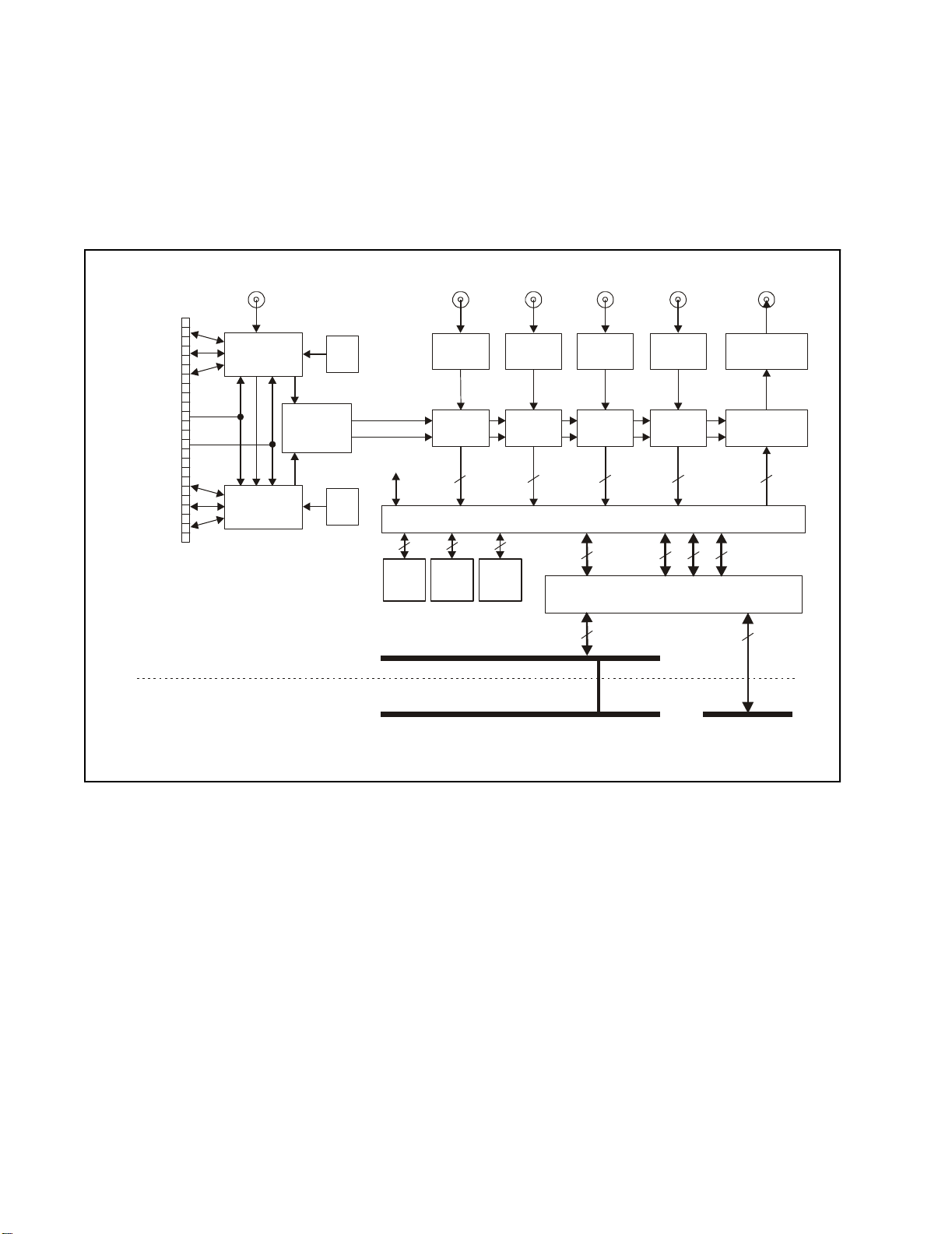
1.4 Block Diagram
The following is a simplified block diagram of the Model 7342, showing the data flow
of the 7142 PMC, through the cPCI carrier.
LVDS Clock A
LVDS Sync A
LVDS Gate A
TTL Gate/
Trigger
TTL Sync
LVDS Clock B
LVDS Sync B
LVDS Gate B
EXT
CLK
TIMING BUS
GENERATOR A
TIMING BUS
GENERATOR B
7142 PMC Module
cPCI Carrier Board
OSC.
SYNC
INTERRUPTS
& CONTROL
OSC.
XTL
XTL
Sync Bus A
Sync Bus B
To All Sections
Control/
Status
DDR
SDRAM
64M x 32
CH 1
RF IN
XFORMER
LTC2255 #1
14−BIT A/D
A/D 1
32 32 32
DDR
SDRAM
64M x 32
PCI BUS (64 Bits/ 66 MHz)
CH 2
RF IN
RF
14
RF
XFORMER
LTC2255 #2
14−BIT A/D
A/D 2
14
Virtex−4 XC4VSX55 or XC4VLX100 FPGA
DDR
SDRAM
64M x 32
cPCI J1
CH 3
RF IN
LOCAL
BUS
PCI 2.2
INTERFACE
RF
XFORMER
LTC2255 #3
14−BIT A/D
A/D 3
14
64
64
CH 4
RF IN
RF
XFORMER
LTC2255 #4
14−BIT A/D
A/D 4
14
32 32 32
Virtex−4 XC4VFX60 or
XC4VFX100 FPGA
DAC
OUT
TRANSFORMER
16−BIT D/A & DUC
FPGA I/O
(Option 104)
cPCI J2
RF
DAC5686
DAC
HI−SPEED
BUSES
64
32
Rev.: B
Figure 1−1: Model 7342 Block Diagram
Page 7

Pentek Model 7342 Installation Manual Page 7
1.5 Principle of Operation
The Model 7342 is a complete software radio transceiver suitable for direct connection
to HF or IF ports of a communications system. Using the popular PMC module format,
it includes four A/D and one D/A converters.
®
The 7342 features a Xilinx
and a Xilinx Virtex−4 XC4VFX60 FPGA (XC4VFX100 with Option 100). The XC4VSX55
(or XC4VLX100) FPGA, identified as the “Signal FPGA” in this manual, can be pre−
configured with one of a variety of optional IP cores to provide signal translation, pro−
cessing, and time delay functions. In addition to pre−configured functions, user−cre−
ated FPGA programming is supported by Pentek's GateFlow
4953 Option 142. The XC4VFX60 (or XC4VFX100) FPGA, identified as the “PCI FPGA”
in this manual, provides board interfaces including PCI. PCI FPGA I/O connections
are provided through the optional PMC P4 connector (Option 104).
Four A/D converters provide input to the Signal FPGA, where the data can be format−
ted, processed or routed to board resources.
Virtex−4 XC4VSX55 FPGA (XC4VLX100 with Option 110)
®
Designer's Kit, Model
The D/A converter includes both interpolation filters and an upconverter stage capable
of producing baseband I & Q or quadrature modulation analog output.
The 7342 includes a large 768−MByte block of DDR2 SDRAM. This memory is con−
trolled by the Signal FPGA and is organized as three 256−MByte banks, 32 Mbyte deep
by 32 bits wide. Separate banks (separate address and data per bank) allow simulta−
neous access to all banks. This memory can be used as buffer memory when transfer−
ring data between board resource or to off−board resources.
The 7342 includes dual onboard crystal oscillators for clocking, but can also accept
external clocks through a front panel MMCX connector. The 7342 is equipped with a
dual LVDS front panel clock and sync bus that can synchronize up to eight modules
with built−in master/termination functions. The bus format is compatible with other
Pentek PMC and VIM modules and will work with the Model 9190 Clock and Sync
Distribution Amplifier for synchronizing up to 80 modules.
Rev.: B
Page 8

Page 8 Pentek Model 7342 Installation Manual
1.6 Specifications
PMC Signal Processing
Refer to the Model 7142 Operating Manual, Pentek document #800. 71420
PMC to cPCI Carrier
Device: Dynamic Engineering cPCI2PMC
PMC Slots: One PMC site
PCI Bus Interface:
Standard: 32 or 64 bit, 33 or 66 MHz
Option 104: 32 bit, 33 or 66 MHz
Power
cPCI Carrier:
With no PMC: (TBD)
7142 PMC:
Current Draw: +3.3V
1.35A 2.5A 0.2A * NC
PMC Power: 16.95 Watts
+5V +12V −12V
* 12V only connected to voltage test circuit
Note: Power estimated with FPGA base circuitry. Power consumption increases
when custom user FPGA designs are added.
Physical
Dimensions: 3U 4HP cPCI card
Weight:
cPCI Carrier (TBD)
7142 PMC 127.6 grams (4.5 oz)
Rev.: B
Page 9

Pentek Model 7342 Installation Manual Page 9
Chapter 2: Installation and Connections
2.1 Inspection
After unpacking, inspect the unit carefully for possible damage to connectors or com−
ponents. If any damage is discovered, contact Pentek immediately at (201) 818−5900.
Please save the shipping container and packing material in case reshipment is required.
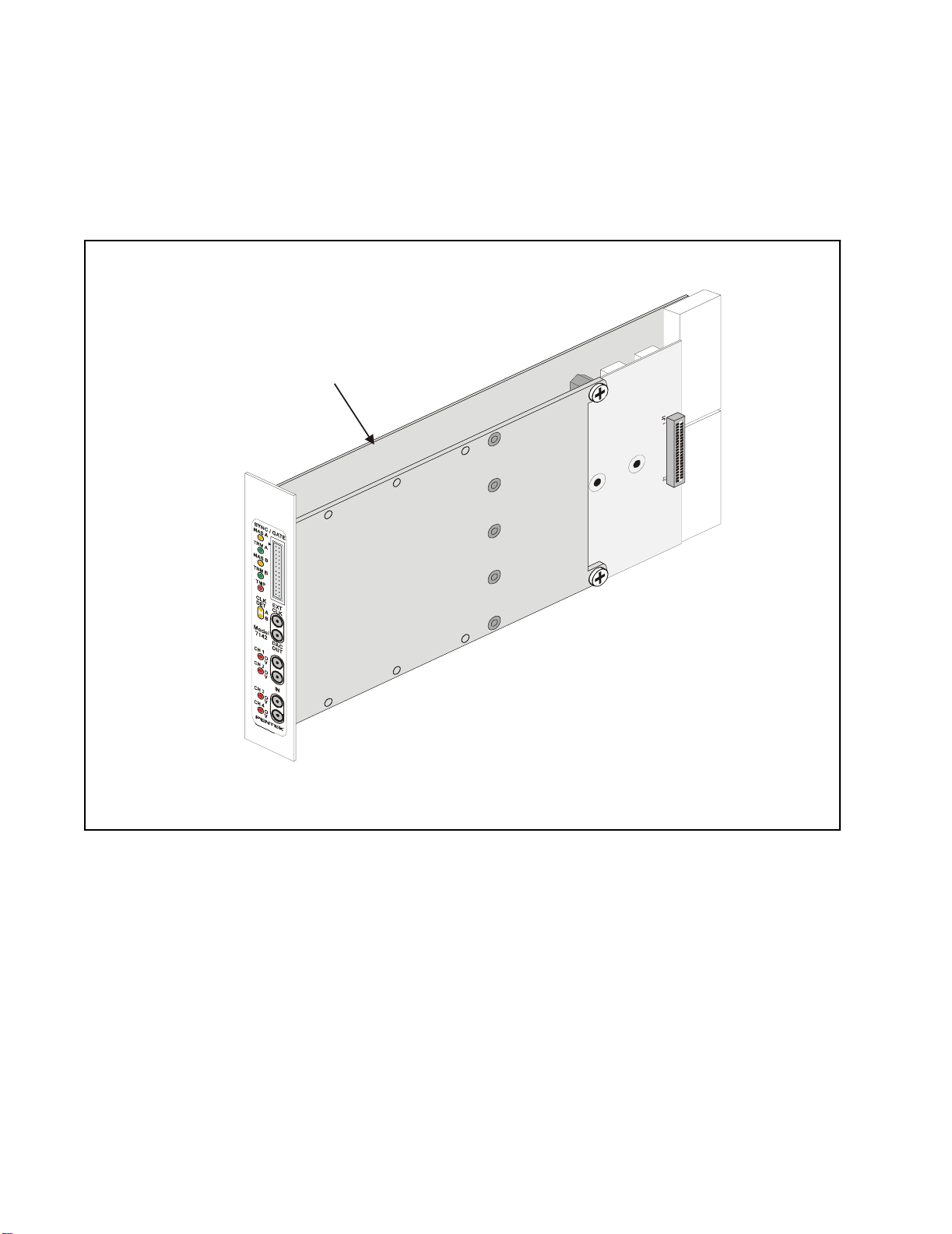
See Figure 2−1, on the next page, for a drawing of the Model 7342 assembly as shipped.
2.2 Jumper Block Settings
The following subsections cover user operating parameters that are set by shorting
jumpers on the Model 7342.
The term jumper (or jumper block) refers to a group of two or more pins on a circuit
board that may be connected in pairs by a shorting jumper to set or change an operat−
ing characteristic of the board. A pair of pins connected in this manner are referred to
as installed, or shorted. A pair of pins that are not connected are called removed, or
open. The shorting jumpers used on the Model 7342 are for 0.020" (0.51 mm) square
pins spaced on 0.079" (2.00 mm) centers. These jumpers are DuPont™ part number
86730−001, or equivalent. Pentek’s part number for these jumpers is 356.00010.
As shipped from the factory, jumpers are installed in default positions on your board.
The default operating parameters they select may or may not meet your requirements.
Before installing your Model 7342, please review the following subsections to deter−
mine whether you need to change any of these settings.
The user should not change jumpers not identified in these figures—these are
Note
The Model 7342 includes one Pentek 7142 PMC module mounted on a Dynamic Engi−
neering Model cPCI2PMC PMC to cPCI 3U carrier. The jumpers on this PMC to cPCI
carrier have been factory set by Pentek for the configuration shipped.
As shipped, the 7142 PMC module is mounted onto the PMC to cPCI carrier. Note that
all jumpers on the PMC are located on the component side of the PMC, and are not
accessible in this shipped configuration. See Section 2.2.3 for the jumper settings for the
7142 PMC. If you need to access a jumper on the 7142 PMC, you must first remove the
PMC module from the cPCI carrier, as described in Section 2.2.1.
reserved for factory test and setup purposes only.
Rev.: B
Page 10
Page 10 Pentek Model 7342 Installation Manual
2.2 Jumper Block Settings (continued)
The following figure illustrates the complete Model 7342 assembly as shipped, with the
7142 PMC module mounted onto the PMC to cPCI 3U carrier.
cPCI
Front
Panel
PMC
Panel
PMC to cPCI
Carrier
7142 PMC Module
J2
J1
Rev.: B
Figure 2−1: Model 7342 Assembly
Page 11
Pentek Model 7342 Installation Manual Page 11
2.2 Jumper Block Settings (continued)
2.2.1 Removing PMC Module from cPCI Carrier
Perform all steps at a static−controlled work workstation.
CAUTION
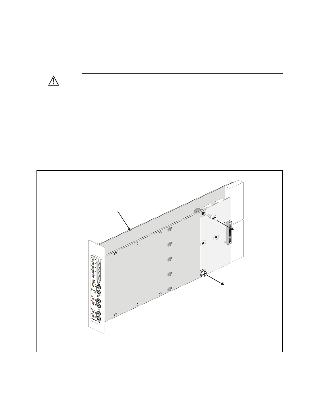
1) From the component side of the Model 7342 assembly (side with the PMC
mounted), unscrew the two pan−head Phillips standoff mounting screws
from the 7142 PMC module (see illustration below).
2) GENTLY, pull on the PMC module to disengage the card’s connectors
from the cPCI carrier’s PMC connectors. Slide the 7142 PMC front panel
out of the opening from behind the cPCI carrier front panel.
PMC to cPCI
Carrier
7142 PMC Module
PMC
Panel
Figure 2−2: Removing PMC Module from cPCI Carrier
J2
J1
Standoff
Screws
You can now access the jumpers located on the PMC module (Section 2.2.3).
Rev.: B
Page 12
Page 12 Pentek Model 7342 Installation Manual
2.2 Jumper Block Settings (continued)
2.2.2 Replacing PMC Module onto cPCI Carrier
After jumper changes, re−install the PMC onto the cPCI carrier as follows.
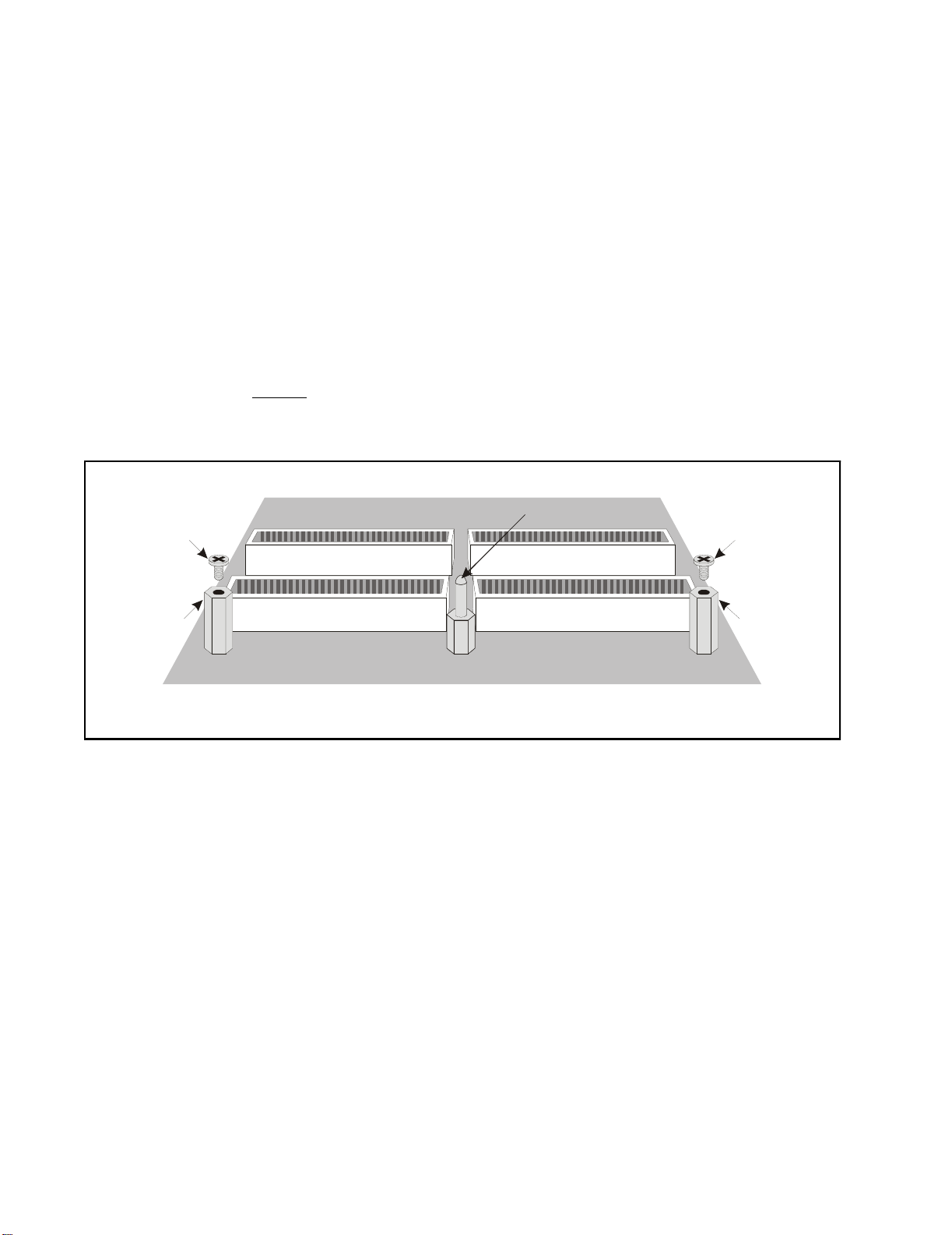
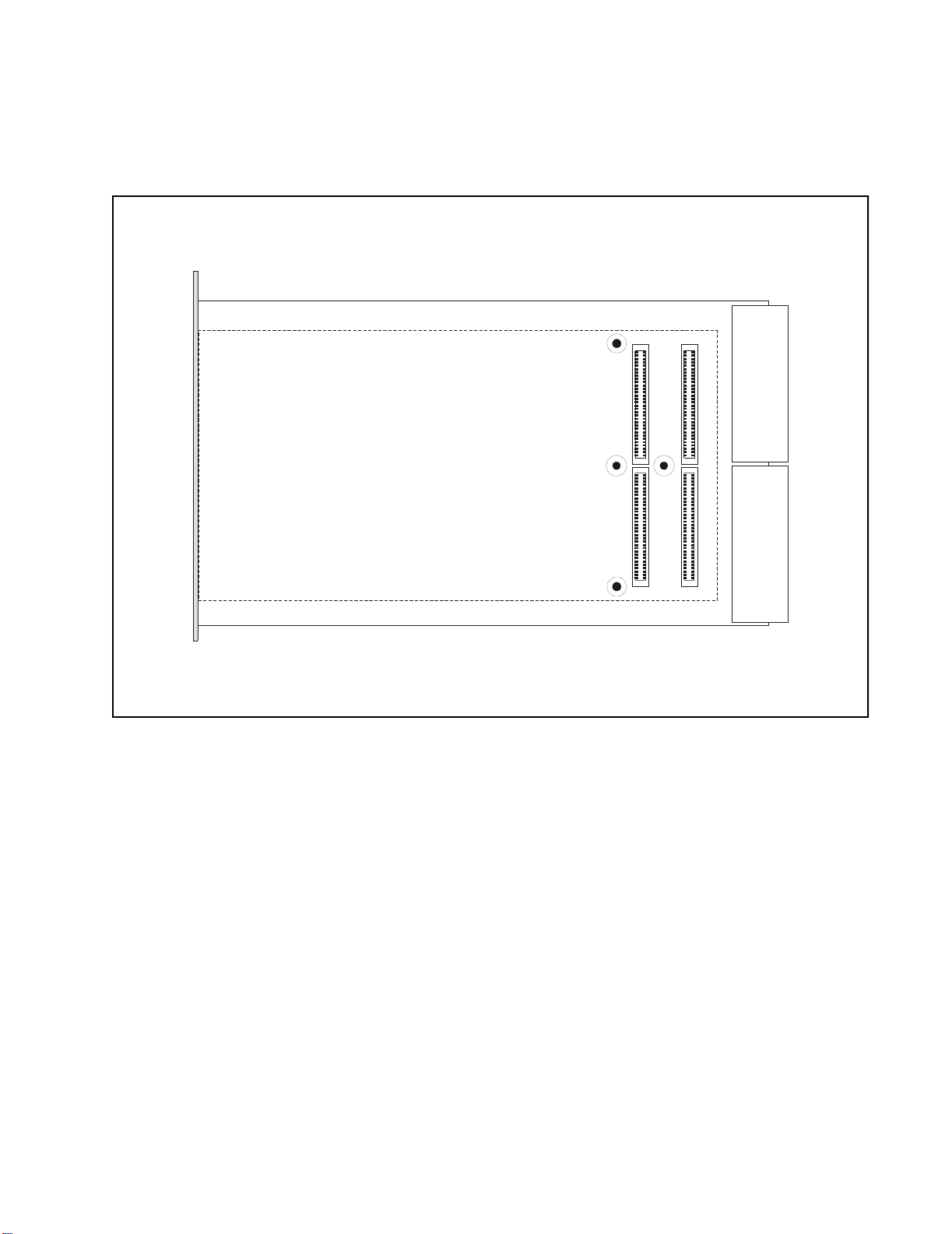
See Figure 2−4 on the following page for illustration of the carrier PCB.
1) Position the 7142 PMC front panel into the opening from behind the cPCI
carrier slot panel (see Figure 2−2 on page 11). Align the PMC module so
that the PMC standoff and key holes on the PMC card are aligned over the
standoffs and PMC key on the cPCI carrier (see illustration below).
Standoff
Screw
PMC
Standoff
NOTE:
For proper operation of the Model 7342, the PMC key must be in
the 3.3V position, as illustrated below.
PMC key
PMC connectors
PMC to cPCI Carrier
Standoff
Screw
PMC
Standoff
Figure 2−3: cPCI Carrier PMC Connections
2) GENTLY but firmly, press down on the areas of the PMC opposite the
connectors to fully seat the card’s connectors into the cPCI carrier. The
four connectors on the underside of the PMC should connect smoothly
with the corresponding PMC connectors on the adapter.
Rev.: B
3) Secure the PMC to the cPCI carrier by screwing the two pan−head Phillips
screws (removed in Section 2.2.1 above) through the standoff holes on the
PMC into the standoffs on the cPCI carrier (see illustration above).
Page 13
Pentek Model 7342 Installation Manual Page 13
2.2 Jumper Block Settings (continued)
cPCI
Front
Panel
1
2
1
2
J2
PMC
Jn1
63
1
Jn2
64
63
2
64
1
2
Jn3
63
Jn4
64
63
64
Figure 2−4: PMC to cPCI Carrier, PMC Connection Side
J1
Rev.: B
Page 14
Page 14 Pentek Model 7342 Installation Manual
2.2 Jumper Block Settings (continued)
2.2.3 7142 PMC Module Jumpers
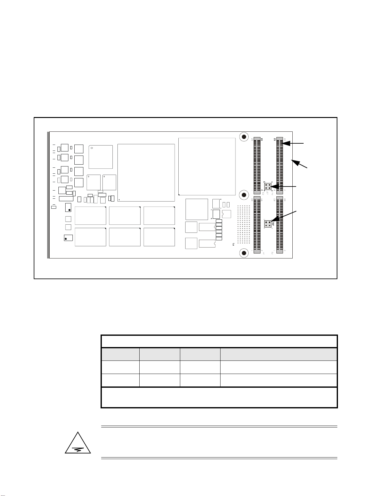
An assembly drawing of the component side of the 7142 PCB is provided
below, showing the jumpers and PMC connectors on the board.
PMC
Connectors
PCB
Revision
320.71420 REV C
Jumper JB1
Front
Panel
Jumper JB2
Figure 2−5: Model 7142 PCB Assembly Drawing, Component Side
Jumper blocks JB1 and JB2, located on the component side of the 7142 PCB
(see Figure 2−5 above), are for factory use only and should not be changed
by the user.
Table 2−1: Factory Default Jumpers
Jumper Pins 1−2 Pins 3−4 Default Function
JB1 Removed * Removed * Factory Use only
JB2 Removed * Installed * Factory Use only
Rev.: B
Note
* Factory Default Setting
NOTE: JB2 is present only on boards identified as Rev C or greater.
DO NOT change these Factory Default jumper settings!
Page 15

Pentek Model 7342 Installation Manual Page 15
2.3 Installing the Model 7342 in a cPCI Card Cage
After the necessary jumpers have been set and the assembly of the cPCI carrier board
and PMC module has been completed (Section 2.2), install the complete Model 7342
assembly into the cPCI Card Cage.
The board is fully compliant with the PCI Local Bus Specification, Revision 2.1.
REMOVE POWER to the cPCI backplane before installation!
DO NOT plug the 7342 into a cPCI backplane with anything other than 3.3V
CAUTION
Refer to Figure 2−1 on page 10 for illustration of the complete Model 7342 assembly.
1) Orient the cPCI chassis on your work surface such that the front panel faces you.
PMC signal levels.
2) Select a vacant cPCI slot in which to install the Pentek 7342 assembly, and remove the
blank cover plate on the front panel.
3) Before touching the Model 7342 assembly, touch the case of your computer's power
supply, to discharge any static electrical charge that may have accumulated on you.
Then, remove the 7342 assembly from its anti−static packaging, and install the card's
connecting edge into the selected cPCI socket.
Be certain that the card edge is properly aligned with the cPCI connector. Gentle
pressure should be sufficient to fully seat the card edge in the connector.
DO NOT ATTEMPT TO FORCE THE CARD INTO THE SLOT! If excessive force
is necessary, then the card is probably misaligned. Damage to either the cPCI
motherboard or the 7342 will be the most likely result of attempts at forced
installations.
4) After the 7342 assembly is fully and properly seated in the cPCI connector, secure the
card's front panel to the cPCI chassis.
This completes the installation procedure.
Rev.: B
Page 16

Page 16 Pentek Model 7342 Installation Manual
2.4 PCI FPGA I/O Connections (Option 104)
Option 104 for the Model 7342 provides connections from the PMC’s PCI FPGA spare
pins to the cPCI J2 connector on the cPCI carrier board (see Figure 2−1). These connec−
tions are programmed for low−voltage differential signals (LVDS) in the default PCI
FPGA configuration—the user can reconfigure these pins with custom FPGA program−
ming.
The 7142 PMC module connects to the cPCI carrier with four 64−pin connectors, desig−
nated P1 through P4 on the PMC (see Figure 2−5). These connectors are defined by the
PMC standard as follows:
• P1 and P2 (PMC Pn1 and Pn2 respectively) contain the 32−bit PCI bus interface
plus associated power, ground, reserved pins, and other necessary signals.
• P3 (PMC Pn3) supports expansion to the 64−bit PCI bus interface.
• P4 (PMC Pn4) supports user−defined I/O, as described below.
With Option 104, the PMC to cPCI carrier routes the 64 signals from the P4 connector of
PMC module to the cPCI J2 connector.
These are available to the user for custom I/O. Table 2−2, on the following page, iden−
tifies the low−voltage differential signals (LVDS) that are connected from the FPGA to
the PMC P4 connector pins on the PMC, and to the cPCI J2 connector pins. Note that
each pin is defined as either input or output from the FPGA, as identified in the table.
Use the FPGA Data In/Out Registers (refer to the Model 7142 Operating Manual,
Pentek document #800.71420, for description of these registers) to read and write LVDS
data using this connector.
• The LVDS_OUT signals in Table 2−2 are from the FPGA Data Out Register, with
LVDS_OUT_x0 from bit D0 and LVDS_OUT_x15 from bit D15.
• The LVDS_IN signals are for the FPGA Data In Register, with LVDS_IN_x0 from bit
D0 and LVDS_IN_x15 from bit D15.
Rev.: B
Page 17

Pentek Model 7342 Installation Manual Page 17
2.4 PCI FPGA I/O Connections (continued)
Table 2−2: Option 104 PCI FPGA I/O Pin Connections
FPGA Signal PMC P4 Pin cPCI J2 Pin FPGA Signal PMC P4 Pin cPCI J2 Pin
LVDS_OUT_P0 1 Row E − 13 LVDS_OUT_P8 33 Row C − 7
LVDS_IN_P0 2 Row D − 13 LVDS_IN_P8 34 Row B − 7
LVDS_ OUT _N0 3 Row C − 13 LVDS_ OUT _N8 35 Row A − 7
LVDS_IN_N0 4 Row B − 13 LVDS_IN_N8 36 Row E − 6
LVDS_ OUT _P1 5 Row A − 13 LVDS_ OUT _P9 37 Row D − 6
LVDS_IN_P1 6 Row E − 12 LVDS_IN_P9 38 Row C − 6
LVDS_ OUT _N1 7 Row D − 12 LVDS_ OUT _N9 39 Row B − 6
LVDS_IN_N1 8 Row C − 12 LVDS_IN_N9 40 Row A − 6
LVDS_ OUT _P2 9 Row B − 12 LVDS_ OUT _P10 41 Row E − 5
LVDS_IN_P2 10 Row A − 12 LVDS_IN_P10 42 Row D − 5
LVDS_ OUT _N2 11 Row E − 11 LVDS_ OUT _N10 43 Row C − 5
LVDS_IN_N2 12 Row D − 11 LVDS_IN_N10 44 Row B − 5
LVDS_ OUT _P3 13 Row C − 11 LVDS_ OUT _P11 45 Row A − 5
LVDS_IN_P3 14 Row B − 11 LVDS_IN_P11 46 Row E − 4
LVDS_ OUT _N3 15 Row A − 11 LVDS_ OUT _N11 47 Row D − 4
LVDS_IN_N3 16 Row E − 10 LVDS_IN_N11 48 Row C − 4
LVDS_ OUT _P4 17 Row D − 10 LVDS_ OUT _P12 49 Row B − 4
LVDS_IN_P4 18 Row C − 10 LVDS_IN_P12 50 Row A − 4
LVDS_ OUT _N4 19 Row B − 10 LVDS_ OUT _N12 51 Row E − 3
LVDS_IN_N4 20 Row A − 10 LVDS_IN_N12 52 Row D − 3
LVDS_ OUT _P5 21 Row E − 9 LVDS_ OUT _P13 53 Row C − 3
LVDS_IN_P5 22 Row D − 9 LVDS_IN_P13 54 Row B − 3
LVDS_ OUT _N5 23 Row C − 9 LVDS_ OUT _N13 55 Row A − 3
LVDS_IN_N5 24 Row B − 9 LVDS_IN_N13 56 Row E − 2
LVDS_ OUT _P6 25 Row A − 9 LVDS_ OUT _P14 57 Row D − 2
LVDS_IN_P6 26 Row E − 8 LVDS_IN_P14 58 Row C − 2
LVDS_ OUT _N6 27 Row D − 8 LVDS_ OUT _N14 59 Row B − 2
LVDS_IN_N6 28 Row C − 8 LVDS_IN_N14 60 Row A − 2
LVDS_ OUT _P7 29 Row B − 8 LVDS_ OUT _P15 61 Row E − 1
LVDS_IN_P7 30 Row A − 8 LVDS_IN_P15 62 Row D − 1
LVDS_ OUT _N7 31 Row E − 7 LVDS_ OUT _N15 63 Row C − 1
LVDS_IN_N7 32 Row D − 7 LVDS_IN_N15 64 Row B − 1
Rev.: B
Page 18
Page 18 Pentek Model 7342 Installation Manual
2.5 Front Panel Connections
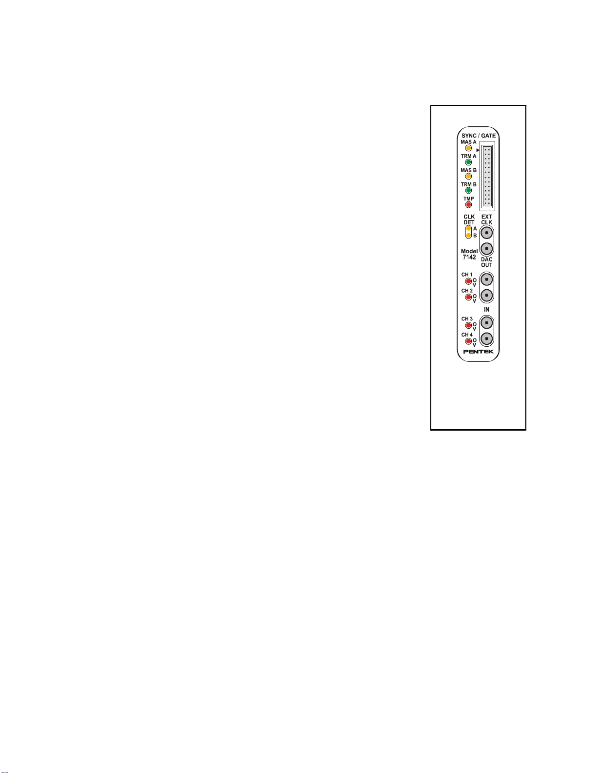
The front panel of the 7142 PMC is illustrated in the figure at
the right. The panel fits into the slot opening on the PMC to
cPCI carrier, as illustrated in Figure 2−1 on page 10.
The front panel includes six MMCX coaxial connectors for
input/output of analog and clock signals, and a 26−pin Sync
bus connector labeled SYNC/GATE. These connectors are
described in the following subsections.
The front panel also includes eleven LED indicators. These are
described in Section 2.6.
2.5.1 Analog Input Connectors CH1 − CH4 IN
The front panel has four MMCX microminiature
coaxial socket receptacles for analog signal inputs,
labeled CH 1, CH 2, CH 3, and CH 4 IN, one for
each A/D input channel.
The analog input signal must be +10 dBm full scale.
Each input drives an RF transformer, with 50 Ω
input impedance.
2.5.2 Clock Input Connector EXT CLK
The front panel has one MMCX microminiature coaxial socket receptacles, labeled EXT CLK, for input of an external sample clock. The external clock signal must be a sine wave of 0 to 10 dBm, with a frequency range from 1 to 125 MHz for ADC use, or from 1 to 300 MHz for DAC use.
The clock can be used as the reference signal to derive the sample clock sig−
nal for the A/D converters and digital receivers. This input is enabled using
the Master Control Register SEL CLK bit (see Model 7142 Operating Manual,
Pentek document #800.71420).
Figure 2−6:
7142 PMC
Front Panel
2.5.3 Analog Output Connector DAC OUT
The front panel has one MMCX microminiature coaxial socket receptacle for analog signal output, labeled DAC OUT.
Rev.: B
The analog output signal is within the range of +4 dBm (−2 dBm with
Option 002). This output is driven by an RF transformer into 50 Ω output
impedance.
Page 19
Pentek Model 7342 Installation Manual Page 19
2.5 Front Panel Connections (continued)
2.5.4 SYNC/GATE Connector SYNC/GATE
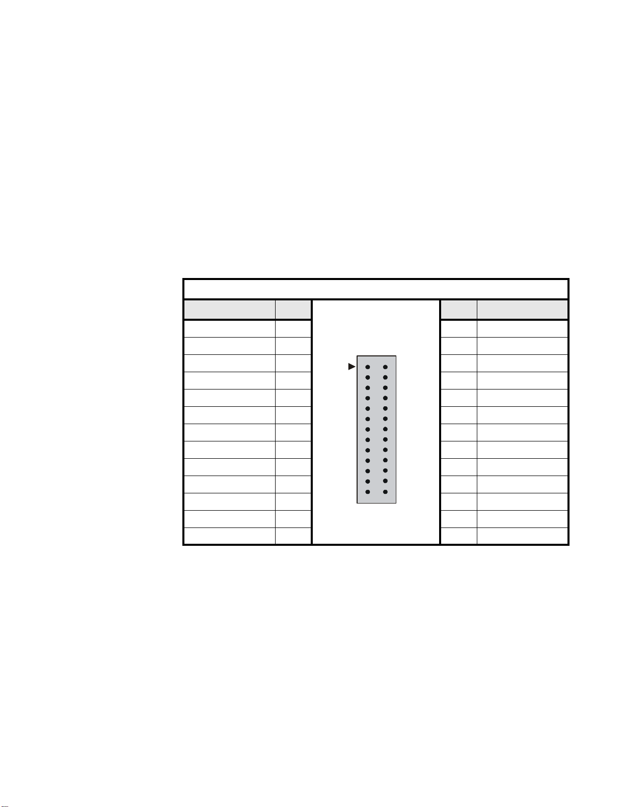
The 26−pin SYNC/GATE front panel connector provides input/output pins
for the low−voltage differential signal (LVDS) timing buses: two indepen−
dent sets of clock, sync, and gate signals. When the 7142 PMC is a bus Mas−
ter, these pins output the buses to other slave units. When the 7142 is a bus
Slave, these pins input all LVDS bus signals from a bus Master. This con−
nector also provides two TTL Gate/Sync inputs. The mating 26−pin con−
nector is Pentek part # 353.02607 (ERNI # 214346).
The following table shows the connector pin configuration.
Table 2−3: SYNC/GATE Connector Pins
Signal Pin Pin Signal
TTL GATE B1 A1 GND
TTL SYNC B2 A2 GND
GATE A− B3 A3 GATE A+
GND B4 A4 GND
SYNC A− B5 A5 SYNC A+
GND B6 A6 GND
CLK A− B7 A7 CLK A+
GND B8 A8 GND
GATE B− B9 A9 GATE B+
GND B10 A10 GND
B1
B2
B3
B4
B5
B6
B7
B8
B9
B10
B11
B12
B13
A1
A2
A3
A4
A5
A6
A7
A8
A9
A10
A11
A12
A13
SYNC B− B11 A11 SYNC B+
GND B12 A12 GND
CLK B− B13 A13 CLK B+
Rev.: B
Page 20

Page 20 Pentek Model 7342 Installation Manual
2.6 Front Panel LEDs
The 7142 PMC front panel has eleven LED indicators, as illustrated in Figure 2−6.
2.6.1 Master LEDs MAS A, MAS B
There are two yellow MAS LEDs, one for each Sync Bus (A or B). The MAS
LED illuminates when this 7142 PMC is the bus Master (see the Master Bus
A/B Control Register, Model 7142 Operating Manual #800.71420). The bus
Master generates all sync/gate/clock signals on the LVDS bus. When only a
single 7142 PMC is used, it must be a Master.
2.6.2 Terminate LEDs TRM A, TRM B
There are two yellow TRM LEDs, one for each Sync Bus (A or B). The TRM
LED illuminates when this 7142 PMC bus is terminated (see the Master Bus
A/B Control Register, Model 7142 Operating Manual). When this 7142 PMC
is the last Slave unit or only unit on the Sync Bus, you must enable bus ter−
mination.
2.6.3 Over Temperature LED TMP
There are several temperature/voltage sensors on the Model 7242 PCB. The
sensor thresholds are set by a PCI interface processor (see TWSI Port Regis−
ter, Model 7142 Operating Manual #800.71420). When an over−temperature
or over−voltage condition is indicated, the red TMP LED illuminates on the
front panel. In addition, an over−temperature/voltage interrupt is available
to a PCI interface processor.
NOTE:
You must set up the temperature/voltage sensors’ serial port
following power on of the cPCI system.
2.6.4 Clock LEDs CLK DET A, CLK DET B
There are two green CLK DET LEDs, one for each Sync Bus (A or B). Each
CLK DET LEDs illuminates when a valid sample clock signal is detected on
the associated Sync Bus. If the LED is not illuminated, then no clock has
been detected and no data from the input stream can be processed.
2.6.5 Overload LEDs CH1 − CH4 OV
There are four red overload LEDs, one for each A/D input, labeled CH1,
CH2, CH3, and CH4 OV. Each LED is an indicator for an A/D overload
detection function in each LTC2255 A/D converter. When an overload
indication is set by the LTC2255, the associated OVLD LED illuminates. In
addition, an OVLD interrupt may be generated from each A/D overload
indication to the PCI interface processor.
Rev.: B
 Loading...