

Page 1
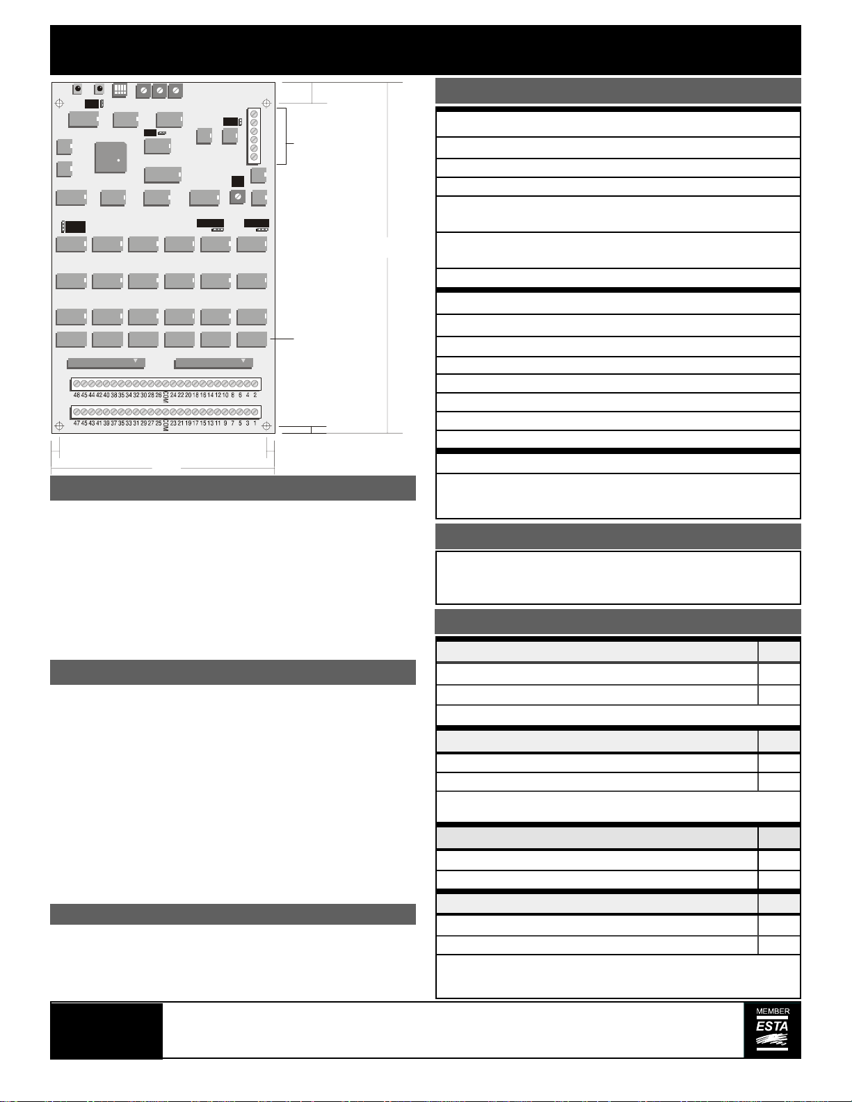
LCDM48 DEMULTIPLEXER Configuration
RxD RUN
S2 S3 S4
S1
JP3
JP2
123
JP6
DP6 DP4
DP5
J3
0.3" 0.3"
JP5
DP3 DP2 DP1
5.6"
J1
V+
COM
COM
CDCD+
ANA
J4
J5
0.75"
POWER/DATA
INPUT
9.0"
DIODE PACKS
0.25"
JP1
P1
JP4
123
123
J2
LED INDICATORS
Two LEDs are used to indicate power supply and processor run
status and data receive detection.
RUN
Glowing steadily indicates power supply and processor
OK; off indicates no power, and flashing indicates defective processor hardware.
RxD
Glowing steadily indicates data signal received; off indicates no signal present. Note that an address selection out of the range of the data signal will extinguish
the LED.
OUTPUT CONFIGURATION
CAUTION:
Disconnect power from the unit before making any
changes.
Before powering up, check to make sure all jumpers are installed correctly. Damage will result if the unit is powered
up with any of the jumpers in the wrong position.
For 4-12V output, install JP1 and JP2.
For 12-15V output, remove JP1 and JP2.
For positive outputs (factory default), jumper pins 2 and 3 of JP4, 5 and 6 and
install diode packs DP1-6 with the notch facing down (left).
For negative outputs, jumper pins 1 and 2 of JP4, 5 and 6, and install the diode
packs with the notch facing up (right as referenced by the above diagram) if you
have MAD1108s or down (left) if you have diodes in carriers.
If J2/J3 are used with DB25 output connectors, install JP3 to reassign the analog
output signals as shown in the Connector Legend Chart, otherwise DO NOT install
JP3.
OUTPUT VOLTAGE ADJUSTMENT
Place the unit in test mode (S1-2 on) and set the address switches to
000 or 001. Ensure that the decoder is connected to dimmer no. 1 and
JP1 & JP2 are in the correct positions. Connect a DC voltmeter between
COM and output terminal no. 1 on the circuit board. Adjust P1 to achieve
the desired full on control voltage.
CONNECTOR LEGEND
CONNECTOR J1
V+
COM
COM
CD-
CD+
ANA
PIN
1-24
25 & 26
PINOUT FOR DB25 CONNECTORS
1-12
13
14-25
12VDC @ 250mA
Power Supply & Signal Common
Power Supply & Signal Common
Signal Input USITT DMX512/AMX192
Data/Clock Complement
Signal Input USITT DMX512/AMX192
Data/Clock True
AMX192 or D54 Analog Input (optional)
CONNECTOR J2,3
Aux. Control Outputs on optional 26 pin DIL header
Channels 1-24(J2), 25-48(J3)
Signal Common
Channels 1-12 (25-36)
Common
Channels 13-24 (37-48)
CONNECTOR J4,5
Analog Control Outputs
Min. 0 to +/-4V Max. 0 to +/-15V
Max. Drive 5mA
(see OUTPUT CONFIGURATION)
ADDRESS SELECTION
Three rotary switches select the offset start address for the unit in most
configurations. In test mode, the switches set dimmers to full one at a
time. The switches are set as (S4) hundreds, (S3) tens and (S2) ones.
DIP Switch Settings
STATUS QUO HOLD TIME
Disabled (2 Sec. timeout) OFF
Enabled ( 5 Min. timeout) ON
Maintains last dimmer levels for set time on loss of input data signal
TEST AND CALIBRATE MODE
Disabled (Normal Operation)
Enabled
When enabled allows analog dimmer outputs to be brought to full one at
a time as selected by the rotary address switches.
PROTOCOL SELECT
AMX192 or D54 OFF
DMX512 ON
DMX TERMINATION
DMX Line Unterminated OFF
DMX Line Terminated ON
This switch connects a 100-ohm resistor across the DMX data pair. The
unit should be terminated if it is the last receiving device on the DMX
line, otherwise leave this switch OFF.
S1-1
S1-2
OFF
ON
S1-3
S1-4
GRAY
rev.6, ver.1.2 release2
Pathway Connectivity, 480C - 36 Avenue S.E.,
Calgary, AB, T2G 1W4 Canada
support@pathwayconnect.com
www.pathwayconnect.com
tel (403) 243-8110 fax (403) 287-1281
Printed in Canada
05/03
 Loading...