

Page 1

Aleph 0s Service Manual Version 1.0 - 1.3
PRODUCT DESCRIPTION
The Aleph 0s is a high performance Mosfet single-ended Class A stereo audio power
amplifier, intended for maximum performance in reproduction of music. It is a simple design,
having only three gain stages: input differential pair, cascoded voltage gain stage, and
output followers. All three gain stages are biased by constant current sources from the
negative supply. The output stage will operate as a single ended class A system at lower
power levels and will operate as a push-pull class A system at levels above the bias point of
the constant current source.
SIMPLIFIED SCHEMATIC
To best understand the operation of the amplifier, refer to the simplified schematic Figure 1.
The front end of the amplifier accepts a balanced or unbalanced input signal at two N
channel Mosfets operating as a differential pair. They are provided with bias by a current
source from the negative rail which operates at a constant 8 milliamps. The output of the
differential pair drives a P channel Mosfet which provides voltage and current gain. At the
output of this second stage you will see the full voltage swing of the amplifier.
This second gain stage is provided with a single-ended Class A current bias from another
current source from the negative supply which provides a constant 30 milliamps current.
Between the current source and the drain of the P channel device is a constant voltage
source which is used to provide voltage bias to the output Mosfet transistors.
The amplifier has complementary N and P channel output transistors operated as source
followers, so that they provide only current gain. High current single ended Class A bias is
provided by yet another constant current source from the negative supply. This current
source provides greater than 1 amp of constant current per channel
COMPLETE SCHEMATIC
For purposes of clarity and simplicity, the complete schematic of the Aleph 0s is broken up
into the following sections: Power supply, Front end, and Output Stage.
Figure 2 shows the power supply schematic. An IEC standard AC line connector connects to
the primary of a toroidal power transformer through an inrush suppression thermistor, fast
blow fuse, a power switch, and a thermostat. Fig 2 shows the transformer wired for 120
VAC, and the transformer can be adapted to 240 VAC by connecting the two primary
windings in series. 100 volt operation requires a special transformer.
The secondary system consists of a bridge rectifier and four 31,000 uF capacitors. The
secondary DC voltage is approximately plus and minus 40 volts. The front end circuitry of
the amplifier is decoupled from the main supply by RC filters.
Figure 3 shows one half of the output stage. Both halves run exactly in parallel.
Page 2
Page 3
Page 4
1
2
3
4
RevNumber
DCBA
1.3
.33
G
S
IRF244
221
R203
221
R204
R206
Q204
MPSA42
C201
4.7
ALEPH 0S OUTPUT STAGE (1/2)
Title
SizeADate
D
Q202
47.5K
R205
.33
R207
ofSheet
Drawn by
PL10OS10.S01
10/10/93 PASS
Filename
V+
Q201
R201
IRF244
221
+D
9.1V
Z201
OUT
R208
9.1V
Z202
Q203
IRF9240
R202
-D
221
ISD
V-
A B C D
1
2
3
4
Page 5

Following are the front end circuits and PC board component placements for Revision
numbers 1.0 through 1.3. All are very similar, and while the following description applies
specifically to Rev 1.0, the comments apply to all versions.
The circuit formed by Q101, Z102, R108 and R107 is a constant current source designed to
bias Z101, the voltage reference for the front end constant current sources, and Q7, the
voltage gain stage cascode transistor. This current source and reference circuit is common
to both channels. Further references are to each channel singly, with both channels having
identical circuits and part references.
Q3 and Q4 are constant current sources which bias the front end. They are driven by Z101
at 9.1 volts, resulting in approximately 4.5 volts across their source resistors, R3 and R10,
giving approximately 8 ma and 30 ma constant current.
The input differential transistors Q1 and Q2 are power Mosfet transistors which have been
matched to .01 volts threshold voltages at 4 milliamps current. The gates of these devices
are connected to differential networks formed by R5, 6, 13-18. These form a true differential
amplifier for balanced input and can be operated unbalanced by simply driving the positive
input (XLR pin 2) with or without shorting the negative input (XLR pin 3) to ground. Shorting
the negative input to ground provides twice the voltage gain over leaving it unterminated,
but either method of operation is acceptable.
Zener diodes Z1 and 2 protect the input transistors from outside transient voltages. Q1
drives Q6 in common source mode which is in cascode (common gate) connection with Q7.
At the same time, Q2 drives the source of Q7 in a folded cascode connection, so that both
input transistors drive the secondary gain stage. The DC offset point of this system is set by
P1.
While the amplifier is primarily biased by the output stage constant current source, the
design provides for "pull" operation beyond the constant current bias point with a set of P
channel source followers. The bias relation between the P and N channel source follower
output devices is set by the constant voltage circuit of Q5 and adjusted by P2. Normally, the
P channel output stage will be biased at about 10% of the value of the constant current
source, or about 100 ma.
C5 provides 10 picofarads of forward compensation in the feedback loop. C6 provides 39 pf
of compensation for Q6.
Z3 provides protection for the gate of Q7 when Q6 is shut down on a negative waveform
clip. Q8 provides current limiting for Q6 during a positive waveform clip.
R1 and C7 provide loading at radio frequencies. If R1 is damaged, it is a sure sign of high
power at high frequencies, such as full power at 100 KHz or Square waves above 20 KHz.
Unless it is on a test bench, the only way the amplifier will experience this will be in system
oscillation, where the output of the amplifier is allowed to bleed back to the input. This is
generally due to wiring fault in the system.
Page 6
1
2
3
4
RevNumber
+DRIVE
DCBA
OUTPUT
C7
.047
C4
390PF
C3
-DRIVE
R1
2.7
GND
ALEPH 0S FRONT END
390PF
ofSheet
PASS
Drawn by
D
PL10FE.S01
12/13/93
B
Title
Size
Date
Filename
Q5
C8
V-
4.7UF
150
R3
Q4
V+
R2
4.75
Q6
Q7
221
MPSA92
4.75K
R109
9.1V
Z102
2.2K
IRFD9210
R7
Q8
39PF
C6
9.1V
Z3
MPSA92
R108
IRF9510
R8
Q101
4.75K
221
R107
15K
CCW
7.5K
R12
Q2
IRFD210
P2
W
IRFD210
5K
GND
C
C5
W
9.1V
Z2
10PF
R18
100K
Q3
R4
R9
IRF610
221
9.1V
Z101
221
680
IRF610
R10
CCW
R11
5K
P1
W
50K
T1
C
W
THERMISTOR
R13
4.75KR5
Q1
IRFD210
4.75K
9.1V
Z1
4.75K
R16
100K
R17
+
R14
4.75K
R15
390PF
C2
390PF
C1
B C
A
R6
221
- INPUT
1
2
221
+ INPUT
3
4
Page 7
Page 8

1
2
3
4
RevNumber
+DRIVE
DCBA
OUTPUT
C7
.047
-DRIVE
R1
2.7
GND
ALEPH 0S FRONT END
PASS
Drawn by
FIG 3
11/6/93
ofSheet
D
PL10FE11.S01
B
Title
Size
Date
Filename
C8
4.7UF
10
R2
Q6
Q7
Q5
Q4
150
R3
221
MPSA92
4.75K
R109
9.1V
Z102
3.3K
IRFD9210
R7
Q8
39PF
C6
9.1V
Z3
MPSA92
R108
IRF9510
R8
Q101
4.75K
221
R107
15K
CCW
4.75K
R12
Q2
IRFD210
W
P2
IRFD210
5K
GND
C
C5
W
9.1V
Z2
10PF
R18
100K
Q3
R4
R9
IRF610
221
9.1V
Z101
221
680
IRF610
R10
10
V+
CCW
R103
R11
5K
P1
W
50K
T1
C106
220 50V
3.3K 2W
R105
C
W
THERMISTOR
R13
4.75KR5
Q1
IRFD210
4.75K
9.1V
Z1
4.75K
R16
100K
R17
+
4.75K
R15
OTHER CH
C105
220 50V
R102
3.3K 2W
R104
10
B C
V-
R14
C2
C1
390PF
390PF
A
R6
221
- INPUT
1
2
221
+ INPUT
3
4
Page 9

Page 10

1
2
3
4
RevNumber
+DRIVE
C4
DCBA
680PF
C3
680PF
2.2K
R?
V+
10
R2
Q6
Q7
OUTPUT
C7
.047
2.2K
R?
C8
4.7UF
Q5
-DRIVE
R1
2.7
Q4
GND
ALEPH 0S FRONT END
Title
Size
V-
150
R3
PASS
Drawn by
11/6/93
B
Date
ofSheet
D
PL10FE.S01
Filename
221
MPSA92
4.75K
R109
9.1V
Z102
2.2K
IRFD9210
R7
Q8
39PF
C6
9.1V
Z3
MPSA92
R108
IRF9510
R8
Q101
4.75K
221
R107
15K
R?
2.2K
R12
C
W
4.75K
Q2
IRFD210
W
P2
5K
IRFD210
GND
CCW
Z2
9.1V
10PF
C5
R18
100K
Q3
R4
R9
IRF610
221
9.1V
Z101
221
680
IRF610
R10
CCW
R11
5K
P1
W
150K
T1
C
W
THERMISTOR
R13
Q1
IRFD210
4.75K
9.1V
Z1
4.75K
R16
100K
R17
+
R14
4.75K
R15
390PF
C2
390PF
C1
B C
A
R5 4.75K
221
- INPUT
1
2
221
+ INPUT
R6
3
4
Page 11

Page 12

1
2
3
4
RevNumber
ofSheet
PASS
DCBA
10
R10
9.1V
Z5
Q6
Q7
+DRIVE
Z3
9.1V
Q5
OUTPUT
C8
4.7UF
C7
9.1V
Z4
.047
-DRIVE
R11
Q4
2.7 2W
GND
Drawn by
PL10FE13.S01
4/25/94
ALEPH 0S FRONT END
B
Title
Size
150
R18
Date
Filename
D
MPSA92
9.1V
Z102
IRFD9210
Q8
39PF
C6
IRF9510
221
R12
R101
15K 2W
R14
33K 2W
R13
VAL
CCW
C4
R8
220 50V
100K
W
P2
IRFD210
5K
C
C5
IRF610
R6
100K
W
10PF
9.1V
Z2
10
R20
R16
R15
221
C9
.1 UF
9.1V
Z101
221
R103
CCW
10
R9
P1
W
C102
220 50V
3.3K 2W
3.3K
5K
Q2
IRFD210
10
R19
Q1
C
W
IRFD210
R7
100K
C3
220 50V
9.1V
Z1
4.75K
R4
100K
R5
4.75K
R3
Q3
IRF610
680
R17
C101
3.3K 2W
R104
220 50V
10
R102
B C
+V
R105
1
2
R2
- INPUT
4.75K
R1
4.75K
+ INPUT
390PF
C1
390PF
-V
A
C2
3
4
Page 13

Page 14

Figure 3 shows the output stage schematic. It shows one-half of one channel's output stage,
which contains 6 output devices. The top IRF244 is an output follower. The bottom IRF244
Mosfet is a constant current source. The P channel IRF9240 transistor is a follower which
contributes beyond the current provided by the constant current source.
On each module, R205 supplies current to Q204, which is the driver for the output stage
active current source. The gate of the output stage current source Mosfet is driven by the
collector of Q204 at about 4.5 volts. This voltage is controlled through current feedback from
the source of the Mosfet connected to the base of Q204. The Base-Emitter junction voltage
of Q204 is about .7 volt, and the circuit operates to hold the source voltages about .7 volt
above the negative rail voltage, which puts .7 volt across the 1.3 ohm source resistor on
each current source Mosfet, which controls 580 ma each times 2 modules, or 1.15 amps
constant current biasing the output stage.
Note that the output devices are matched for Gate to Source voltages at 200 ma on all
transistors to within .1 volt. This means that all IRF9240 devices within an amplifier are
matched, and that all IRF244's used as output followers are matched, and all IRF244's used
as constant current sources are matched. The match voltage of each transistor is written on
the case at Pass Labs, and ranges from 3.00 to 4.99. If it is necessary to replace devices in
the field, they must be a match. Devices with a particular number may be obtained from
Pass Laboratories.
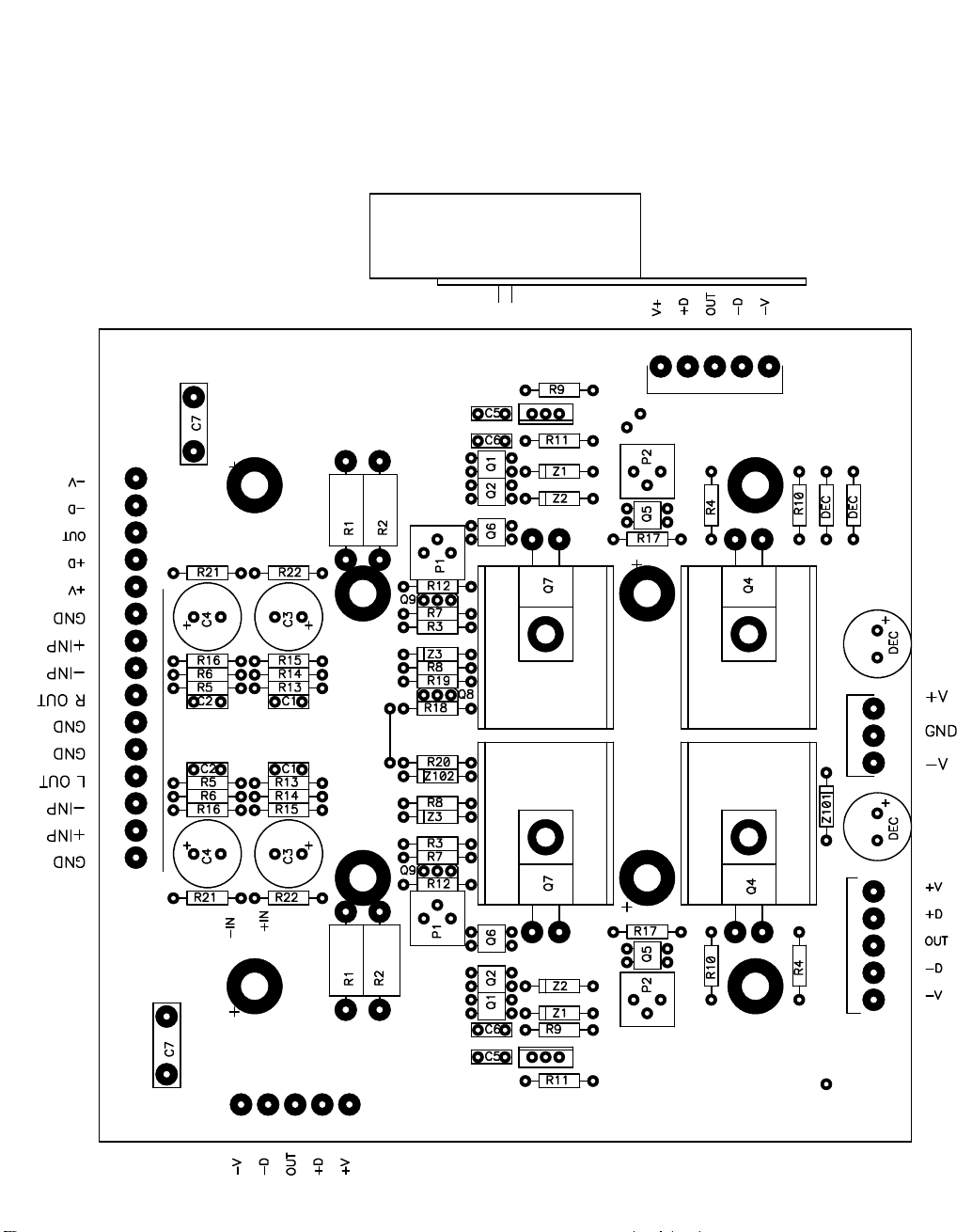
Figure 5 shows the PC layout of the front end board. Note that the control and power
connections to the output stage are through wires connected by screw-down terminal
connectors. The wires coming off the main board are attached to the output stage modules
by corresponding connections.
ADJUSTMENTS AND SERVICE
Initial power up procedures: For an amplifier in unknown adjustment or being powered up for
the first time after repair or modification.
Essential Equipment: Oscilloscope, Audio signal source, Variable AC power source, AC line
current meter, 8 ohm load.
A distortion analyzer is very helpful confirming proper operation, but is not essential to
adjustment of an otherwise working amplifier.
If you do not have an AC line current meter, you may place a .1 ohm 5 watt power resistor in
series with the AC line (cold) and measure the voltage across it (1 amp = .1 volt AC), taking
care not to electrocute yourself.
Page 15

Check the AC line fuse
Set signal source to .1V at 1 KHz
Attach signal source
Attach 8 ohm load.
Monitor the amplifier output with oscilloscope, Set the AC line source to 0.
AC power switch on
P1 (offset adjust) should be at mid-position.
P2 (bias adjust) should be at mid-position.
Slowly turn up the AC line voltage to 1/3 while watching the current draw.
Rated power draw: 1.4 A avg. @ 120 VAC, .7 A avg. @ 240 VAC
Rated power draw: 1.4 A ~ 120 V ~ 1.4 (power factor) = 240 Watts
You will see the amplifier draw current near to rating when the AC line voltage is at 1/3
rating or more. At 1/3 AC line voltage, adjust P2 for minimum current draw (maximum
resistance for P2). At this position, the power draw of the amplifier will be that of the output
stage constant current source.
Different means of measurement of AC current draw will give slightly different results.
However the constant current source of the output stage draws most of the power in the
amplifier and is quite accurate. On a working amplifier it may be used as the basis or norm
for current measurement.
If the DC offset at the output is excessive, then you should adjust P1 on the front end
board. Initially this will usually be set to middle. P1 will have to be readjusted after a
warm-up period of at least an hour.
If the power draw is correct and a clean 2 volt signal appears at the output and DC offset is
minimized, then the amplifier probably works. You may slowly increase the AC line voltage
to full rating while watching the output wave form and the current draw.
Then increase the signal level to full output of the amplifier, verifying proper operation up
to clipping. With the bias set to minimum, there will be some distortion at higher power
levels, which is expected.
Page 16

After you have verified that the amplifier will drive an 8 ohm load to 40 watts, you can set the
bias point. It is quite easy. First, make note of the current draw of the amplifier with both
channels at minimum bias and with the amplifier cold. Multiply this figure by 20%. Then
without a load or signal, idle the amplifier for an hour or more. Noting the minimum current
draw after warm-up, adjust P2 of one channel so that the current draw is one half the
difference between the warm value and 1.2 times the cold value. Then adjust P2 of the other
channel so that the current draw is not 1.2 times the cold minimum draw.
Typical example: The cold AC current draw with the bias at minimum is 1.2 amps. Let the
amplifier warm up for at least an hour. Now the bias will be 1.0 amps. Set the bias P2 of one
channel to one-half the difference between the 1.0 amps and 1.2 amps plus 20%, or 1.44
amps. One half of the difference in this case is 1.22 amps, so set the first channel for 1.22
amp AC line draw. Now set the second channel so that the AC line draw is now 1.44 amps.
At the factory, we set 120 volt units for 1.4 A average AC line draw, with 1.6 A for 100 volt
line, and .7 A for 240 volt line. Your voltmeter might be different, which is why we have the
above procedure. When you are done, the warmed up amplifier should draw AC line current
which is 20% more than the minimum possible line draw with the amplifier cold.
Any questions, call the factory.
The DC offset must be readjusted after warm-up also, setting it as close to 0 DC as
possible. The DC offset will drift for an hour after this, and must be set again.
Probably the least precise performance parameter of the Aleph 0s is the DC offset at the
output, and this relates to the single-ended nature of the design and the pure DC approach
to the circuitry.
On a warmed-up amplifier, the offset will generally be 50 mV or so, but it will show cold DC
offset of 300 mV or even more. The DC offset must be final adjusted after the amplifier has
been allowed to warm up for an hour (heat sink temperatures of 50 degrees C. or so). The
top assembly of the amplifier must be closed up during operation.
After adjusting, check the DC offset at half hour intervals, readjusting if necessary. At the
factory we monitor the offset during a three day burn in, and we expect it to stay within 100
mV with an ambient temperature between 70 and 80 degrees F. At higher ambient
temperatures the offset voltage will drift positive, and at lower ambient temperatures it will
drift negative. It is permissible and preferred to adjust the offset against a known ambient
temperature.
Page 17

Notes on transistor matching
Input Mosfets (IRFD110 or IRFD210) must have their threshold voltages matched to about
10 mV at 4 ma of current. This is accomplished by attaching the gate to drain and passing 4
ma of current through the device, typically with a 13.8 volt source and 220 ohms resistance.
The voltage from the gate/drain to the source is measured. The devices to be matched must
be under the same conditions and temperature.
Output Mosfets (TO-3 packages) must be matched to within 100 mV at 200 mA of current.
The same procedure applies, except that 50 ohm and 13.8 volts is used.
When requesting single transistors from the factory, note the threshold voltage of the
device, which is written on it.
No transistors in TO-220 packages must be matched.
Pass Laboratories prefers to supply power transistors in matched sets, but if you need to
replace a one or more devices, be certain that the numerical code matches.
Even if the numerical code matches, at the factory we test the current going through all
transistors by measuring the voltage across the source resistances in operation. This
absolutely insures the integrity of the match and also catches any other output stage
connection or transistor failure.
Page 18

PERFORMANCE SPECIFICATIONS
Gain 26 dB balanced (50 Ohm Source)
26 dB unbalanced (50 Ohm Source)
Freq. Response 0 dB @ DC -3 dB at 100 KHz
Power Output 40 watts @ 8 ohms 20 Hz - 20 KHz
80 watts @ 4 ohms 20 Hz - 20 KHz
160 watts @ 2 ohms 20 Hz - 20 KHz
Distortion <1 % THD
Maximum Output 25 amps ( pulse), 30 volts (peak)
Output impedance .02 ohm @ 1 KHz @ 8V @ 8 ohm
Balanced input 12 Kohm, differential
Common mode rejection 60 dB @ 1 KHz @ .1V input common ground
Output Noise 10 nanowatt, 20 - 20 KHz, unweighted
(-95 dB, ref. 40 watts)
DC offset 100 mV after warm-up, balanced mode
Power Consumption 250 watts at idle
Operating Temperature 50 degrees C.
Warm up time 1 hour minimum
Page 19

1 0/20/95
Aleph 0s Service Manual Update Rev 1.4
Comments:
The Aleph 0s revision 1.4 gives the circuit the same topology as the Aleph 1, using all N
channel devices in the output stage. The input impedance is increased, and the RCA input
connection offers 20 or 26 dB of gain depending on the presence of the jumper between
pins 1 and 3 of the XLR input.
The published distortion and power specs remain the same, but the circuit actually shows a
bit lower distortion.
Adjustments are made to four potentiometers through a single hole in the center of the top
cover. Offset adjustment occurs by P101 and P201. Bias adjustment occurs by P102 and
P202.
Bias is adjusted for a total AC line draw of 2 amps RMS (120 volt) or 1 amp RMS (240 volt)
or 2.4 amps (100 volt). The bias pots are adjusted so that the bias current is essentially
equal between the channels, giving the same distortion curve between the two channels.
It is absolutely essential that the AC line current be measured in true RMS for bias
adjustment.
If a distortion analyzer is not available, start with both bias pots all the way down, and
apportion the difference in current between the two channels to give the proper AC line
draw current. If the amplifier is cold, set the bias 10% high, to allow a decline during
warmup.
The amplifier DC offset and bias must be adjusted again after 1 hour warmup. If significant
adjustment is necessary after an hour, the adjustment is repeated after another half hour.
Page 20

1
2
.47 3W
D
S
R132-3
3
4
1.4
RevNumber
ofSheet
PASS
1 1
.47 3W
D
S
R134-5
Drawn by
DCBA
+ SUPPLY
+46V
G
Q110-1
R128-9
IRF244
221
9.1
Z107
+ DRIVE
+ OUT
C103
.047
R123
22.1K
R127
3.3 3W
- OUT
221
R121
G
221
IRF244
R130-1
9.1
Z108
D
ALEPH 0S AMPLIFIER
PL10FE14.S01
4/10/95
Q112-3
B
Title
Size
Date
Filename
- DRIVE
CURRENT
FEEDBACK
15K
R125
R124
221
10K
R126
475
S
D
R122
Q109
-46V
- SUPPLY
MPSA42
CCW
68.1
9.1
Z104
5K
P101
W
R111
3.32K
R110
G
IRF9620
Z106
R120
Q108
221
IRF610
Q104
G
R117
S
221
D
221
R118
9.1
S
Q105
G
IRFD9210
D
Q106
S
G
R112
IRF9620
D
221
D
Q107
2.21K
R114
10PF
G
C
S
IRFD210
W
W
5K
P102
CCW
R106
9.1
100K
Z103
15K
R113
100PF
9.1
Z105
C
W
C102
C101
Q102
D
D
Q101
G
IRFD210
S
S
G
221
R109
221
R108
9.1
Z102
9.1
Z101
D
R116
Q103
IRF610
B C
221
G
681
S
R119
IRFD210
10K
R104
15K
R115
100K
R105
10K
R103
C-60
1K
R107
RCA
INPUT
1
R102
XLR3
2
10K
10K
XLR2
R101
XLR1
TH1
GNDEARTH
3
4
A
Page 21

 Loading...