

Page 1
Balanced Zen Line Stage
Copyright 1997 Nelson Pass
Introduction
The popularity of the Zen projects points out the interest in very simple
linear circuits. They are intended to fuel that interest. The Zen, Bride of
Zen, and Son of Zen have been explorations in how much objective and
subjective performance can be achieved with a single gain stage. This
extreme simplicity has an aesthetic appeal, which speaks to the purist in
audiophiles, and the presumption that simple circuits sound better.
At least one "objectivist" has complained (objected?) that the Zen
projects do not measure up compared with more sophisticated and
complex amplifiers. This is mostly true, but beside the point. The
literature and store shelves are full of multi-stage amplifier circuits using
generous amounts of negative feedback.
These are single stage amplifiers.
Getting good performance from a single gain stage is a fine technical
challenge, and I would say a proper beginning for those who would go
on to design and build more complex circuits. Simple circuits have
particular value as DIY projects. They are more understandable, they
are more likely to be attempted, and they are more likely to work.
So is this the anticipated Bride of the Son of Zen? I suppose it is. It has
an identical topology and is perfectly suited for driving the Son of Zen,
but there is much utility to this circuit. It also serves as a nice balancedin to unbalanced-out or unbalanced-in to balanced-out converter.
Like the Bride of Zen and the Son of Zen projects, this circuit performs
linear amplification without negative feedback. A lot has been written
pro and con about the use of negative feedback, and I don't propose to
bring the debate into this article. It just so happens that we will be
getting quite good performance without it.
Being that the noise picked up from the environment is usually common
to both input lines, it is rejected at the input of the balanced circuit, and
thus is much less of a problem. Actual home audio systems using
balanced interconnects typically have about 1/10 the background noise
and hum.
Another reason to use balanced preamplifying gain stages is that many
high end DAC designs offer balanced outputs in which separate DAC
circuits are used for each of the two phases of output. Using separate
balanced DAC circuits reduces the random noise by 3 dB, the same as
if they were in parallel, and reduces common noise by a larger figure.
There is also the potential for reduction of distortion with such an
approach, but to realize the full performance of these circuits, the gain
stage following must have a balanced input.
The Design
This balanced line stage is the classic "differential pair" topology with
two identical gain devices connected to develop voltage gain from a
differential voltage input. The gain devices (tube/bipolar/fet) couple to
each other through their Cathode/Source/Emitter pins. The voltage
input is presented to the Grid/Gate/Base pins, varying the current
through the devices, and showing up as balanced output voltages on the
Plate/Drain/Collector pins.
By the way, unfortunately the designation of Source pin for a MOSFET
is often confused with the use of the word "source" which occurs
frequently in reference to audio. For clarity here, I will always capitalize
the "S" when referring to the pin.
Balanced Operation
Let's review why balanced operation is desirable. Audio circuits operate
in an environment of electrical noise; crosstalk from other channels,
ground loops, magnetic pickup from transformers, power supply ripple
and other noises. In a balanced circuit, two opposite phases of the
signal are present on two otherwise identical input lines. The input of a
balanced circuit has a plus and minus polarity, and the output of the
circuit also has a plus and minus. The balanced amplifying circuit will
amplify the difference between the two inputs and will display a larger
difference signal at the output.
What the circuit doesn't do is as important as what it does; it does not
amplify any portion of the signal which is the same at both inputs.
Ideally it completely rejects the common input signal, and the quality of
this rejection is referred to as the Common Mode Rejection Ratio
(CMRR), which tells how much of the common input signal gets through.
Pass D.I.Y Project: Balanced Zen Line Stage page 1
fig.1
Page 2

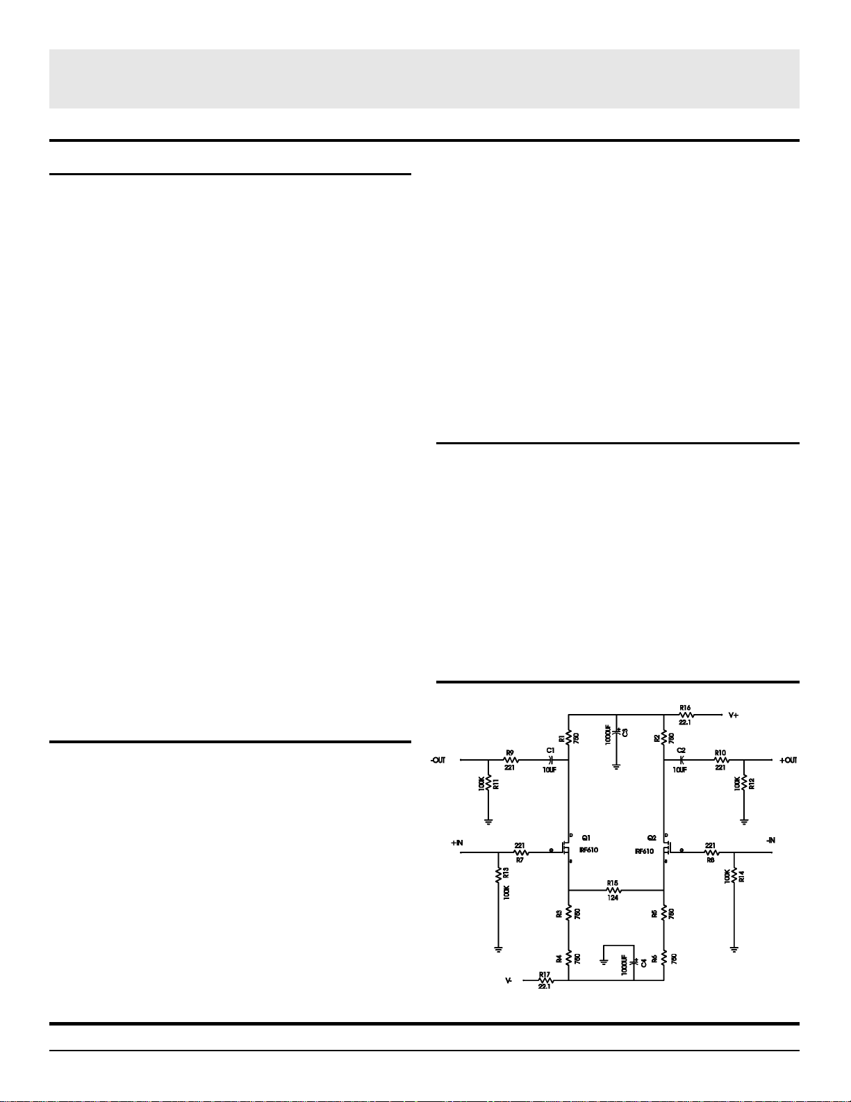
Figure 1 shows the circuit for one channel. Q1 and Q2 are the active
elements of the gain stage. They are mutually coupled through R15,
and the current through them is controlled by the differences in their
Gate voltages. The Gates are nominally at ground through R13 and
R14, and the transistors are biased through resistors R3, R4, R5, and
R6 connected to a negative voltage supply. Balanced output signals
appear on the Drain pins of Q1 and Q2, loaded by R1 and R2 connected
to the positive supply.
At the output Drains of Q1 and Q2 we will see a DC potential of
approximately one-half of the positive supply, and the two voltages will
vary in opposite phase. The maximum peak-to-peak voltage at each
Drain is the value of the positive supply, and twice that amount when
considered as a balanced output. As a practical matter these two
paraphase outputs are passed to the outside world through capacitors
which block the DC voltage.
The circuit amplifies a differential input to a differential output. Given a
single input, it will amplify it into a balanced differential output, and is
useful to convert unbalanced signal to balanced, either because you
wish balanced operation or because you wish to convert a conventional
stereo amplifier into mono bridged operation.
Of course the circuit is happy accepting a balanced input, and besides
using it as simply a balanced gain stage, you can choose to view either
output polarity as a single-ended output of each phase. Thus the circuit
also functions as a general balanced and unbalanced converter.
Referencing Figure 1, we note the function of various components.
Resistors R7, R8, R9, and R10 serve to slightly isolate the inputs and
outputs from the transistor pins, preventing parasitic and other types of
oscillation. The values for these resistors can range from 100 to 475
ohms, and 221 ohms is about the best value.
Resistors R13 and R14 serve to provide a reference to ground for the
input pins in case there is no source or in case the source is AC coupled.
This keeps the Gate voltages near ground so that the amplifier biases
with the proper DC voltages and currents. Similarly, R11 and R12 serve
to bleed off the DC voltage which initially appears at the output through
the blocking capacitors C1 and C2.
R16, R17 and C3, C4 are used to passively filter the supply voltages.
The supplies will be regulated, but the filter will remove stray and
residual noise at the output of the regulators. The circuit itself will reject
supply noise through balanced operation, but this does not help when
using a single phase of the output. Passive supply filtering improves
both balanced and non-balanced operation.
Resistors R1 through R6 are all 750 ohm metal film power resistors
rated at three watts each. All the other resistors in this project are ¼
watt metal film types. R1 and R2 serve as the loads for the transistors,
and R3, R4, R5 and R6 are used to bias the circuit with a current source
from the negative power supply. The reason I used two 750 ohm 3 watt
resistors in series was to get a 1500 ohm 6 watt resistor with the same
part as used for R1 and R2.
fig.2
Pass D.I.Y Project: Balanced Zen Line Stage page 2
Page 3

The gain of the circuit is the ratio of the impedances of the output circuit
divided by the impedances of the circuit that couples Q1 and Q2. The
summed impedance of the output circuit is essentially R1 plus R2, and
is 1500 ohms. The impedance of the coupling circuit is 124 ohms
summed with the approximately 12 ohm apparent source resistance of
each of the MOSFETs, or about 150 ohms. The gain of 10 (20 dB)
reflects the 1500 ohms divided by the 150 ohms. You can adjust the
gain of the circuit arbitrarily by adjusting the value of R15 without
affecting the quiescent DC values of the circuit. As you decrease the
value of R15 to 0 ohms, the gain will approach 50 (34 dB). As you
increase the value of R15, the gain decreases, with 430 ohms giving 10
dB of gain. Some of the performance curves presented later will reflect
both 10 and 20 dB gain settings.
Figure 2 shows the power supply for the circuit. Because the voltages
required by this project are higher than delivered by off-the-shelf
transformers, I have chosen to use two transformers T101 and T102
with secondary circuits in series, one for the positive and one for the
negative supply. The primary circuits are connected in parallel, in this
case showing 120 VAC operation. The regulated supply voltages at the
outputs of this power supply will be at 60 volts each, and to give us an
adequate margin from the unregulated supply, I have chosen AvelLindberg transformers model D4007, rated at 30 + 30 volts AC on their
secondaries and 30 watts each. The AC secondary voltages are
rectified through B101 and B102 to produce an unregulated plus and
minus 80 volts DC.
The circuit is protected by a 1 amp slow blow fuse, and a high voltage
(AC line rated) filter capacitor C107 is placed across the line to reduce
noise. Earth ground from the AC cord is attached to the chassis for
safety, and is connected to the circuit ground through a power thermistor
(bright idea from Frank DeLuca). This gives some resistive isolation for
prevention of ground loops but goes to small values of resistance in
case of catastrophic connection to the live AC line.
The unregulated 80 volt rails are cleaned up by pass transistors Q101
and Q102 acting as voltage followers from stacks of Zener diode voltage
references. The Zener diode stacks are 7 X 9.1 volts, or about 63.7
volts, fed a trickle of current by R101 and R102. Allowing for the
approximately 3.7 volt loss from MOSFET Gate to Source pins, the
output of Q101 and Q102 are 60 volts DC. Capacitors C103 and C104
across the Zener stacks reduce the noise, as do capacitors C105 and
C106 at the output of the supply.
Zener diodes Z115 and Z116 are used to protect the Gates of the
MOSFETs from exceeding the 20 volt limits imposed on the Gate-toSource rating of the MOSFETs. As elsewhere, the Gates of the
MOSFETs are isolated through resistors R103 and R104 to prevent
parasitic oscillation.
It is possible to set up the power supply to regulate at lower voltages to
match transformers with less voltage than offered by the D4007's
specified. Alternately, you might choose a single transformer that does
not develop as much voltage as two D4007's. Simply replace some of
the Zener diodes with shorting wires to produce lesser reference
voltages in increments of 9.1 Volts, or replace the 9.1 volt parts with
other values. To give you a picture of performance at lower supply
voltages, I have documented the distortion curves for voltages of 30, 40,
50, and 60 volts on each rail.
At 60 volt regulated rails, each channel draws 80 mA of bias current (40
mA passing through each MOSFET in the gain circuit). This is about 10
watts per channel. You can power two channels off this supply, or you
can choose to give each channel its own power supply. The current
drawn by the gain stages is roughly proportional to the supply voltages,
so that the circuit draws about half the current with 30 volt rails.
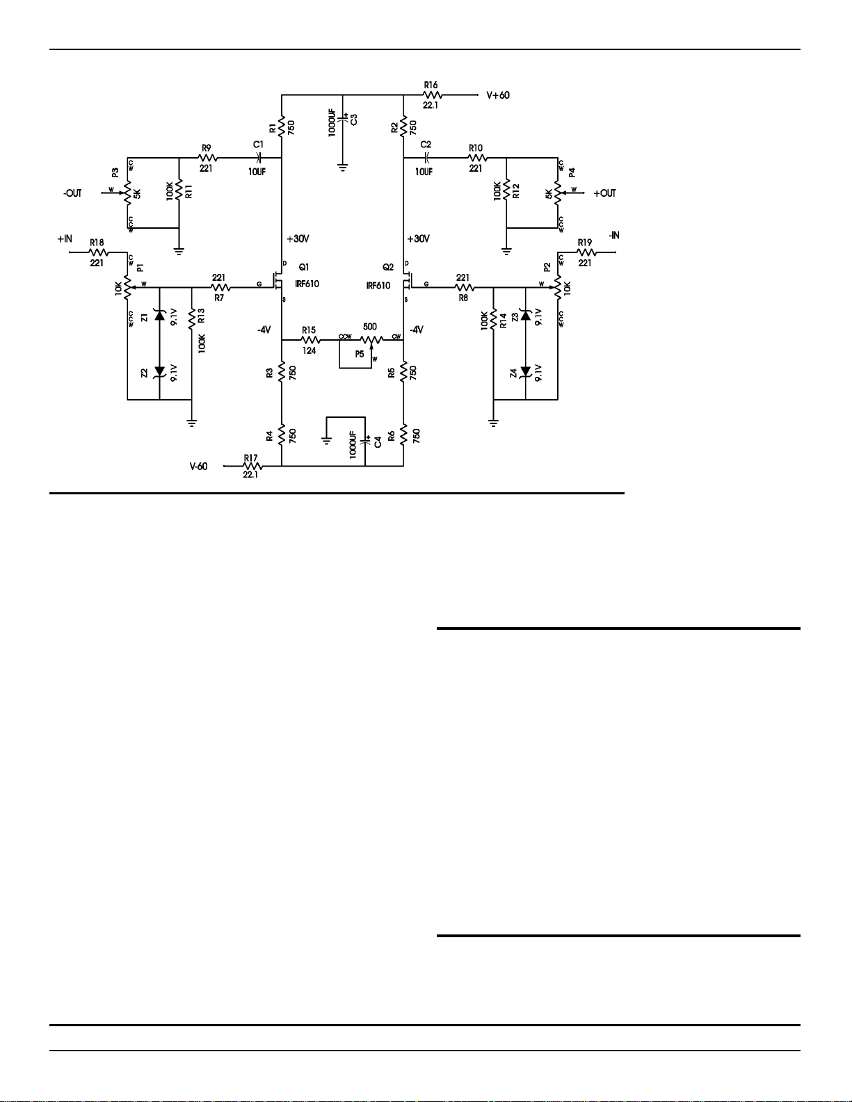
Figure 1 shows a perfectly workable version of the gain stage, but I can't
resist tarting it up a bit with some protection and gain controls. Figure 2
shows the circuit with these added. Zener diodes Z1, Z2, Z3 and Z4
form input protection networks which prevent input voltages in excess of
9 volts or so. Higher values can be used, with 16 volt Zener diodes
being the practical limit. It is not essential that the input protection
diodes be used, but without them greater care will be necessary in
connecting signal sources.
There are four potentiometers also shown if Figure 3. P1 and P2 can be
used to attenuate the input signal. Because the balanced input
characteristic is perfectly preserved if P1 and P2 are set at the same
value, they perform best as precision ganged controls, but this is not
essential otherwise. P1 and P2 can be used to protect the input from
higher voltage signal sources, or they can be used as volume controls.
P3 and P4 perform attenuation at the output, and can also be used
either as a volume control or simple gain adjustment. P3 and P4
attenuate the output noise of the circuit as well.
P5 allows intrinsic adjustment of the circuit gain without having to match
the potentiometer values, and as shown with a 500 ohm potentiometer,
allows adjustment from about 10 to 20 dB gain.
The use of any of these potentiometers is optional and independent of
each other. The value of the potentiometer is flexible with the value
given as optimal for typical use. Ideally P1 and P2 are the same value,
and P3 and P4 are the same value in order to preserve the CMRR
figure.
Part List
Components from Figure 3, the main circuit, are numbered from 1 to 99,
and represent one channel only. Components from Figure 2, the power
supply, are numbered from 100 to 199. You can use the power supply
board to power both channels, or you can use two power supply boards,
one for each channel. You will note on the PC board layouts that two
separate sets of input power connections, one for each channel, are on
the main PC board to facilitate use of one or two power supplies.
With the exception of the power transformer and the PC board, the
components used in this project are available from Digikey (800) 344
4539, and I have included the appropriate Digikey part numbers for
parts. Digikey handles the Yageo metal film resistors, I used Dale
RN55D types.
In general, a wide variety of substitute parts will be acceptable so long
as they have the appropriate wattage and voltage ratings. The
MOSFETs used are fairly generic N channel devices in TO-220
Pass D.I.Y Project: Balanced Zen Line Stage page 3
Page 4
packages, and substitutes should have a 100 volt rating. The IRF610 is
rated at 200 volts, 20 watts, and 10 amps. An excellent substitute is the
IRF510. Devices of higher current or wattage rating are not preferred,
as the capacitance of the device is increased correspondingly, and
results in degraded performance at high frequency, although I have
been able to get acceptable performance out of 150 watt devices with
10 times the capacitance.
degrade the quality.
Substitute capacitors should
have a 100+ volt rating. Many
do-it-yourselfers have called
me up and explained the
wonders of various better parts,
capacitors, resistors, wires, and
diodes, that I could have
specified that would improve a
project. Some of you have
been kind enough to send
samples, which I much
appreciate. Oddly, nobody
sends me better transistors,
and considering that gain
devices account for most of the
distortion, this is what I would
really prefer.
As a rule, I like to leave the
more exotic parts out of these
designs, and I have several
reasons. First, I want to make
fig.3
this as simple and inexpensive
as possible for most of you.
Second, exotic parts are not the
particular point that I am trying to emphasize in these projects; rather it
is the quality that can be achieved with very simple approaches.
Most important, I have saved these embellishments for you to perform
independently.
Part List for Main Board (one channel only)
It is not essential to match the MOSFETs used in this project, but it
doesn't hurt either. I have tested the circuit with matched and random
parts with insignificant performance differences. There are other circuits
that take advantage of matching, but because of the separate bias
sources for each device and the high value of resistance between the
Source pins of the two devices, this circuit is indifferent to matching. The
exception is the case where R15 has a small value for the purpose of
very high gain. Under this circumstance, matching will improve
performance, and I recommend Vgs matching to within .1 V or better.
For the procedure on matching devices, see one of the previous
MOSFET project articles either in the pages of AE or on the Pass Labs
website.
Potentiometers P1 through P4 are nominal values, and you should feel
free to use parts that are similar in value. P1 and P2 determine the input
Designation Part Digikey #
Q1, Q2 IRF610 N channel MOSFET IRF610-ND
Z1-4 (optional) 1N4739 9.1 V Zener diode 1N4739ACT-ND
P1-2 (optional) 10 Kohm Potentiometer 381N103-ND
P3-4 (optional) 5 Kohm Potentiometer 381N502-ND
P5 (optional) 500 ohm Potentiometer 381N501-ND
C1-2 10 uF film capacitor EF1106-ND
C3-4 1000 uF electrolytic P6476-ND
R1-6 750 ohms @ 3 watts P750W-3BK-ND
R7-10 221 ohm ¼ watt metal film 221XBK-ND
R11-14 100 Kohm ¼ watt metal film 100KXBK-ND
R15 124 ohm ¼ watt metal film 124XBK-ND
R16-17 22.1 ohm ¼ watt metal film 22.1XBK-ND
R18-19 221 ohm ¼ watt metal film 221XBK-ND
Heat sinks (2) 1 watt sinks for TO-220 HS104-1-ND
impedance if used. While you might feel that it is desirable to use very
high values so as to have a high input impedance, keep in mind that the
input capacitance of the MOSFETs puts a natural upper limit on the
Part List for Power Supply Board
value, so for best performance I don't recommend exceeding 25 Kohms.
Similarly, P3 and P4 will influence the output impedance, and as you use
higher values, the output impedance goes up. Lower values of output
potentiometers will reduce the gain of the circuit, but not otherwise
Designation Part Digikey #
Q101 IRF610 N channel MOSFET IRF610-ND
Q102 IRF9610 P channel MOSFET IRF9610-ND
Pass D.I.Y Project: Balanced Zen Line Stage page 4
Page 5
B101-102 Diode Bridge 2KBP02M-ND
Z101-116 1N4739 9.1 V Zener diode 1N4739ACT-ND
C101-102 1000 uF electrolytic P6476-ND
C103-106 10 uF electrolytic P5593-ND
C107 .047 uF Line filter Capacitor P4637-ND ACline rated)
R101-102 4.75 Kohm ¼ watt metal film 4.75KXBK-ND
R103-104 221 ohm ¼ watt metal film 221XBK-ND
TH101 Thermistor KC006L-ND
Heat sinks (2) 1 watt sinks for TO-220 HS104-1-ND
F101 1 amp fuse, slow blow F319-ND
Fuse Holder panel mount 3AG WK0002-ND
AC Power Inlet -- Q212-ND
T101-102 D4007 30 + 30 volt Avel Lindberg
Tel (203) 355 4711 Fax (203) 354 8597
PC board
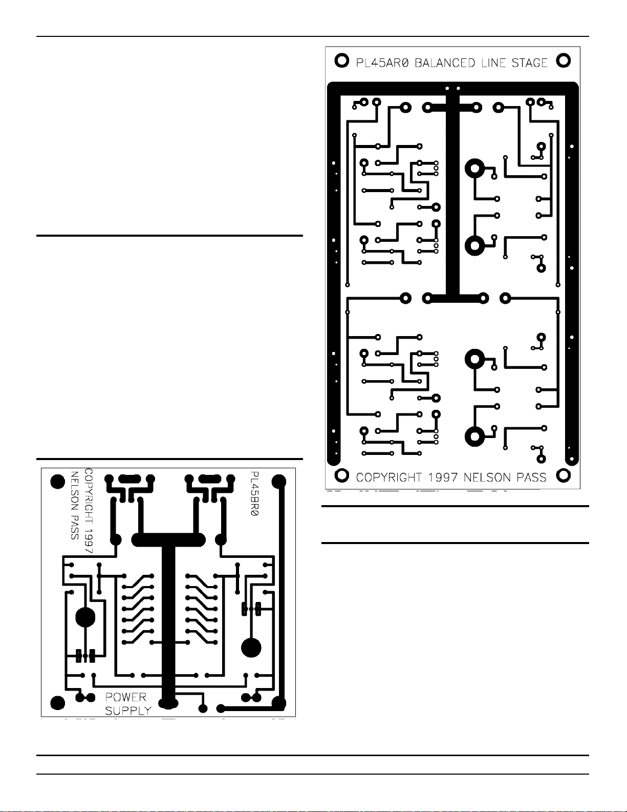
Figures 4 and 5 show the PC board layout for both the channels and the
power supply. Figure 4 is laid out to give two balanced channels. Note
that the artwork is seen from the copper clad side, not the component
view. Note that on Figure 4 the references R1, etc. are identical for each
channel. For two channels you will want two R1's and so on.
Figures 6 and 7 show the stuffing diagrams for these two boards. This
view is from the component side, which is the mirror image of the PC
artwork.
For those of you wanting to have a production house make boards for
you, the website www.passlabs.com has the zipped Gerber files for
these boards available for downloading. Keep in mind that this is a
simple enough circuit to be wired up point-to-point, and if you have
difficulty obtaining the circuit boards, I encourage you to use this
approach. This is in fact what I did with the first version of the circuit,
and it worked perfectly.
fig.4
Construction Notes
All the resistors in the project are ¼ watt 1% metal film types. My
personal preference is Dale, but there are many good, possibly better
types. If you decide to go crazy and use Vishay or other exotic parts,
the circuit might sound better; it is very unlikely to sound worse, and no
matter what you do, the result will still probably be much cheaper than
buying a readymade preamp.
The main PC board shows jumper wires where the pads are designated
for P5. Naturally if you use P5, you will replace the jumpers with wires
leading to P5.
There are two sets of power supply connections, one for each channel,
and this allows the use of one supply for both channels, or two separate
supplies, one for each channel. In any case, you will be using separate
fig.5
wires to bring the supply voltages into the main board.
Pass D.I.Y Project: Balanced Zen Line Stage page 5
Page 6

introduce distortion, although I have to say that I have not measured any
substantial distortion, nor have I been able to identify it subjectively. Bad
Zener diodes will definitely create distortion, however, and this effect is
more common than you would think.
Speaking of input and output connections, I have not specified
connector types for this project. Usually for this sort of project I use both
XLR and RCA connectors on both the inputs and outputs. The inputs
are female XLR with pin 2 = plus, 3 = minus, and 1 = ground. At the
output it is a male XLR connector. In parallel with the XLR connectors
are 2 RCA connectors, one for each polarity, with XLR pin 2 connected
to the "live" of the positive RCA and pin and XLR pin 3 connected to the
"live" of the negative RCA. XLR pin 1 is attached to the grounds of both
RCA connectors. These grounds are isolated from chassis ground. The
case of the XLR connector, if metal, and shield are attached to chassis
ground.
The power transformers used here are toroidal types having dual
primary and dual secondary windings. The schematic shows secondary
output wires A, B, C, D for each transformer which will attach to the
ABCD designations on the power supply board. The colors coming out
of the Avel D4007 are: A = Black, B = Red, C = Orange and D = Yellow.
It does not matter which transformer goes to which set of connections,
as they are identical. You will note that B and C wires are simply tied
together (on the PC board) for each transformer and do not connect to
anything else.
fig.6
Heat sinks are provided for each power MOSFET, as they tend to run
hot otherwise. On the board layout you will see that they are fairly small,
and are designed to lay down on the board with a #4 or #6 screw and
nut securing the transistor and heat sink to the board. Note that the
metal portion of the TO-220 case is attached to the Drain pin of the
MOSFET, and so both the case and the heat sink are electrically live.
A word to the wise is always appropriate when discussing the use of
MOSFETs: they are sensitive to static discharge. Gate-to-Source
voltages in excess of 20 volts have the potential to damage or destroy
these parts. Take some care to avoid unnecessary handling, and avoid
static electricity while handling. A modest amount of care in this regard
is generally adequate, and when the MOSFETs are installed in the
circuit, they are pretty safe if you are using the Zener input protection
diodes.
The wiring for the primary AC side of the transformers is not provided on
the PC board, and must be accomplished point-to-point. I strongly
suggest that you use standard safety rated AC inlet connectors and fuse
holders.
Remember safety first. The Earth ground going back to the AC outlet in
the wall is connected to the chassis, and then the circuit ground is
And why wouldn't you use the input protection diodes? I suppose you
could imagine that they reduce the "purity" of the circuit and potentially
Pass D.I.Y Project: Balanced Zen Line Stage page 6
fig.7
Page 7

connected to the chassis or earth ground through the power thermistor
TH101. Do not neglect this connection. It is very important that the
chassis be earth grounded and that the circuit ground be attached also
to earth ground, either through or without the thermistor. Note that the
earth side of the thermistor connects to the chassis through the
mounting pads of the power supply board. It will be important to use
metal standoffs here and check the connection with an ohmmeter or
otherwise hardwire the connection of thermistor to chassis ground.
C107 is an interference filter capacitor across the AC line. It is optional,
but if you decide to use such a capacitor, make certain that it is safety
rated for the AC line. Also be certain to wire it in carefully, avoiding
potential for short circuit to chassis or other components.
The primary windings of the transformers shown in Figure 2 are for 120
volt operation. Blue = 115A, Grey = 0A, Violet = 115B, and Brown = 0B.
In this case we see that two sets of four wires each will be attached to
the AC power, so that both primary windings of each of the two
transformers see 120 volts AC. This is accomplished by tying two each
Blue and Violet primary wires together (Blue + Blue + Violet + Violet) at
the Hot side of the AC line. The cold side of the AC line is attached to
the Grey and Brown primary leads of each transformer in a similar
manner.
For 240 volt operation, the Grey and Violet leads are tied together, not
attached elsewhere, on each transformer, so that the two primary
windings are in series. The Blue leads of the transformers then go to the
hot AC line, and the Browns go to the cold. Don't leave the Grey/Violet
leads sitting bare if you do this.
Keep in mind that not only the primary AC line side of the power supply
has potentially lethal voltages, but the secondary system is high voltage
as well. Use extreme caution; there are few enough Do-it-yourselfers as
it is. If you don't feel competent to handle this end of it, get some help.
Most technicians have low resistance to a smile and/or a six pack of
beer.
Firing up the circuit for the first time is no big deal. Preferably you use
a Variac ™ to raise the line voltage a little at a time to check for excess
current draw or smoking components. If you don't have a Variac ™ you
will simply plug it in and stand back.
It is possible to test the power supply board without the main board.
Simply load the V+ with 15 Kohms ¼ watt to ground and the V- with 15
Kohms to ground and look for the 80 volt values on the plus and minus
rails and the 60 volt values on the plus and minus regulated rails.
A few voltage points will be helpful, all referenced to ground:
volts. The Gates of Q1 and Q2 should be at ground. The Source pins
of Q1 and Q2 should be about -3.5 volts or so.
If you get these voltages, everything should be just fine.
Several points about operation:
If you have elected not to use input protection Zener diodes Z1-4, then
you will want to be quite careful when you plug sources into the inputs.
Generally this means touching the ground of the interconnect cable to
the ground of the female connector or to the chassis before inserting the
plug. The input Gates of the MOSFETs can take 20 volt peaks. I have
seen them withstand 80 volt transients, but not reliably. If you don't use
the Zener diodes, but do use P1 and P2, then you can always turn the
potentiometers to 0 (counter clockwise) during connection.
Also note that if you do not use Zener diodes for input protection, you
will not need R18 and R19, and they may be replaced by wire. Their
function is to ensure stability for the circuit driving the input, since
directly looking at a Zener diode can drive some circuits into oscillation.
This is also why we use R7 and R8, and R9 and R10.
If you blow out a MOSFET, nine times out of ten it will be excess GateSource voltage.
Speaking of transients, I have not provided for turn-on transient
suppression at the output of the preamp circuit. As with the Bride of Zen,
to avoid potential damage to a loudspeaker, you should ensure that the
power amplifier is turned off when the preamp is powered up, or if you
have chosen to use P3 and P4, you can reduce the output to 0. The
output transient is balanced, by the way, so that it is much lower in value
when evaluated differentially.
A turn-on/off suppression relay would be a nice add-on project. I invite
interested parties to send their design to Audio Electronics magazine.
If you elect to use P1-5 to adjust the parameters of the circuit, you can
gain quite a bit of flexibility in its use. In general, the best performance
occurs with the higher value of P5, giving 10 dB gain instead of 20 dB.
If you don't need the gain, use 10 dB.
Adjusting the input signal level using P1 and P2 will allow you to
optimize the operating point against the signal source level. The best
performance occurs at approximately 1 or 2 volts output of the circuit
(assuming P3 and P4 are turned up all the way). If you are running 10
dB of gain, this means an input level of .3 to .6 volts, and if your source
has much higher output, you can turn down P1 and P2 so as to set the
input level to this region.
The Drain (case) of Q101 should be +80 volts DC or so. The Drain of
Q102 should be approximately -80 volts.
Once you have obtained the optimal gain and input level, adjusting the
output level with P3 and P4 will give you an effective volume control
which attenuates circuit noise as well as level. Of course you can use
The output of the supply V+ and V- should be plus and minus 60 volts
DC. This can be seen on the Source pins of Q101 and Q102, or on the
output voltage pads.
any of these pots as volume controls as you like. Keep in mind that the
common mode rejection figures depend of the matching of the values of
P1 and 2 and separately P3 and P4. If you are particularly concerned
about this figure (and I am not) you might consider using a precision dual
On the main board the Drain (case) of Q1 and Q2 should be about +30
pot for these.
Pass D.I.Y Project: Balanced Zen Line Stage page 7
Page 8

Performance
voltages. The distortion climbs smoothly with the output voltage, and
clipping is graceful.
Below the 1 to 2 volt region, increasing noise drives the curve upward.
This noise figure works out to about a 5 microvolt input noise (-106 dbV)
or about 17 nanovolt-per-square-root-Hertz input noise floor. This is
comparable to your typical noisier variety of FET op amps.
fig.8
Figure 8 shows the distortion waveform of the circuit at 1 KHz at 1 volt
output. Note the second harmonic character of the distortion waveform.
This is generally regarded as the most desirable of the harmonics, that
is to say, if you have to have distortion, second harmonic is the least
objectionable. Those well versed in circuit design might immediately
comment that we expect to see third and other odd ordered distortion
components in the distortion, given the symmetric nature of the
balanced circuit. Odd ordered harmonics begin to dominate at higher
levels of output, but at a couple of volts and below, we see even
harmonics due to the subtle mismatching of the semiconductors.
fig.9
Figure 9 shows the THD (Total Harmonic Distortion) & Noise
performance of the circuit for output voltages from 100 mV to about 30
volts. This circuit has an R15 value of 124 ohms. Four curves are
shown, reflecting the performance for 30, 40, 50 and 60 volt rails, and
as you can see, performance is enhanced by the higher rail voltages and
bias currents. Unless otherwise indicated, results reflect the 60 volt
rails.
The circuit has a high voltage output, about the same as a 100 watt
amplifier at the 1% distortion figure. It is not likely to be used at these
numbers, but is a part of getting linear performance down at low output
fig.10
Figure 10 shows the performance with R15 at 430 ohms, for a gain of
10 dB. The distortion is lower by a factor of about 10 dB (no surprise),
and the output noise is reduced by the same amount, reflecting the
same input noise.
fig.11
Figure 11 shows the THD & noise, again for four different rail voltages.
The output is at 2 volts and is plotted versus frequency. The figure is the
same from 20 Hz to 20 KHz.
Figure 12 shows the frequency response, measuring -1 dB at 200 KHz
at the top end. The graph does not show the low frequency rolloff, which
would be worst case -3 dB at 4 Hz for a 10 Kohm load with a 5K value
for P3 and P4. Without P4 and P5 and with a 10 Kohm load, the rolloff
is about 1.5 Hz.
The slew rate of the circuit itself is exceedingly high; it does not have a
slew rate as such, but rather a classic RC risetime which is dependant
on the capacitance seen at the output interacting with the resistive
output impedance. The rolloff for the approximately 1000 ohm output
Pass D.I.Y Project: Balanced Zen Line Stage page 8
Page 9
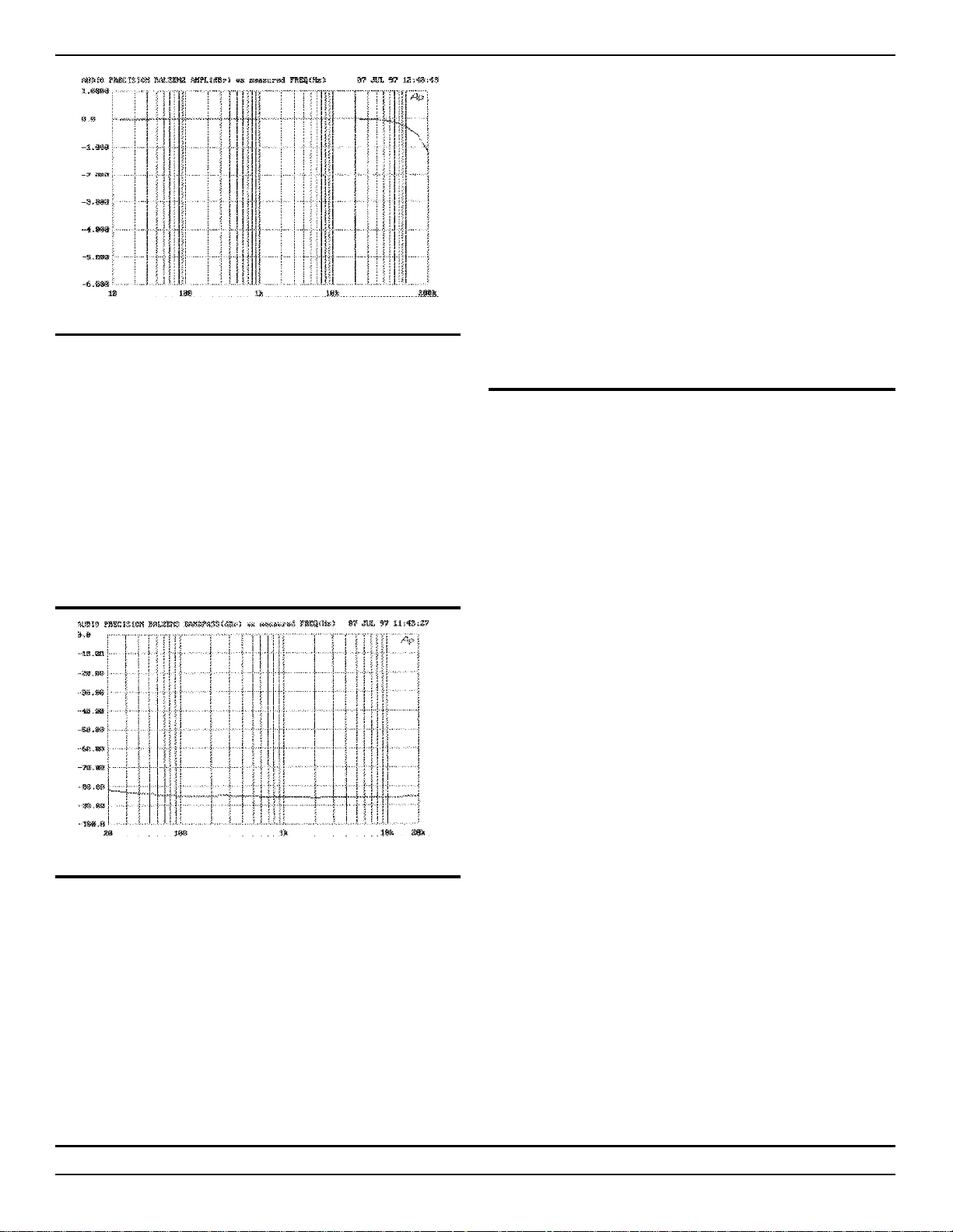
fig.12
will be about 166 KHz into 1000 pF. Lower values of output impedance
can be obtained by loading the output to ground, but at the expense of
voltage swing. For example without P3 and P4, loading the output with
1000 ohms will drop the output swing by half, but will double the high
frequency roll-off point. As there is plenty of output swing, we can safely
throw some away if a higher rolloff frequency is required.
This particular circuit, like the Bride of Zen, will not distort into low
impedance loads; the gain simply goes down. As a result, you can
safely drive 600 ohm balanced loads, getting the same performance as
with a comparable input voltage, but at a lower output level. This is
because the distortion figure is a function of variation in current through
the MOSFETs, which is independent of the load impedance.
one polarity of the output signal, you will find the rejection is only about
a factor of 10 (-20 dB). Obviously this isn't nearly as good, but in point
of fact it still represents a factor of 10 better than an unbalanced circuit,
and usually this is plenty. I have read assertions that 60 dB CMRR
figures are the minimum acceptable, but no good reason to why this
figure is essential. In my book, any reduction of noise picked up is a
plus.
In actual practice with real systems, I have noticed that there is usually
about a 20 dB difference in background noise between balanced and
unbalanced systems, and a circuit with 20 dB rejection will preserve this
difference fairly well. As an alternative to having to use the balanced
output only, you can replace the resistors R3, R4 and R5, R6 with 40 mA
active constant current sources. This will restore the 80 dB CMRR
figure for unbalanced output.
Conclusion
This is a particularly good sounding circuit, and I think it sounds
significantly better than the Bride of Zen, although I would be hard
pressed to explain why. It seems more liquid and has greater depth,
while BOZ is a bit dry by comparison. It might be distortion cancellation
in the balanced circuit, or it might be the greater dynamic range afforded
by quieter balanced operation and higher output swing. As always, I
encourage you to build it and decide for yourself.
Comments and questions are welcomed. The best way to reach me is
by e-mail through the Pass Labs website, www.passlabs.com, or more
directly: nelson@ passlabs.com. This method gets a reliable, if short,
response.
fig.13
One of the figures of merit for balanced circuits is called the Common
Mode Rejection Ratio (CMRR). As previously mentioned, one of the
benefits of balanced circuitry is that it amplifies input differences while
ignoring or rejecting common signal (noise). The CMRR of this circuit is
slightly greater than 80 dB, as illustrated in Figure 13, which shows the
performance from 20 Hz to 20 KHz. This is a factor of about 10,000 to
1, so that a 1 volt common input comes out as about .0001 volt when
measured differentially at the output.. This figure was achieved with
unmatched gain devices, but careful matching does not significantly
improve the performance.
Snail mail is Pass Labs, PO Box 219, Foresthill CA 95631.
This pretty well finishes the preamp offerings in the Zen series. Next:
the penultimate Zen amp.
Copyright 1997 Nelson Pass
This figure was achieved differentially at the output. If you are using only
Pass D.I.Y Project: Balanced Zen Line Stage page 9
 Loading...