

Page 1

GF200 Service Manual GF200
GF200 Service Manual
(GSM Cellular Phone)
Pantech Co., Ltd., Korea
June 28, 2004
1st Edition
For Use by Authorized Service/Maintenance Personal Only
Documents to Receive This Addendum:
GF200 Maintenance/Repair/Operating Manual
Page 2

GF200 Service Manual
CONTENTS
SECTION 1 INTRODUCTION .............................................................................................................3
1.1 INTRODUCTION..............................................................................................................................3
1.2 FREQUENCY ALLOCATION AND ITS USE ...........................................................................................3
1.3 ITEM NAME AND USE ..................................................................................................................... 4
1.4 CHARACTERISTICS ........................................................................................................................4
SECTION 2 ELECTRICAL SPECIFICATIONS....................................................................................5
2.1 GENERAL ......................................................................................................................................5
2.2 TRANSMITTER…………………………………………………………………………………………….5
2.3 RECEIVER…………………………………………………………………………………………………5
SECTION 3 OPERATION....................................................................................................................6
3.1 NAME OF EACH PART…..……………………………….…………………………………………………6
3.2.DISPLAY ..………………….…………………………….………………………………………………..7
3.3 KEYPAD …………………………………….………….………………………………………………..7
SECTION 4 THEORY OF OPERATION..............................................................................................8
4.1 LOGIC SECTION........................................................................................................................8
4.1.1 DC DISTRIBUTION AND REGULATION PART…………………………………………………………….8
4.1.2 LOGIC PART…………………………………………………………………………………………….8
4.1.2.1 SUMMARY…………………………………………………………………………………………….9
4.1.2.2 BASEBAND DIGITAL SIGNAL PROCESSING………………………………………………………….10
4.1.3 MEMORY PART………………………………………………………………………………………..12
4.1.4 NOTIFICATION PART..................................................................................................................13
4.1.5 KEY PAD PART .........................................................................................................................13
4.1.6 LCD MODULE(DISPLAY PART) ..................................................................................................13
4.2 RADIO TRANSCEIVER SECTION.....................................................................................................14
4.2.1 DC DISTRIBUTION AND REGULATION PART.................................................................................15
4.2.2 TRANSCEIVER PIN DESCRIPTION…………………………………………………….……….15
4.2.3 RECEIVE SECTION………………………………………………………………………………….…17
4.2.3.1 AN OVERVIEW OF RECEIVE SECTION ......................................................................................17
4.2.3.2 RECEIVER PART……………………………………………………………………………….……18
4.2.4 TRANSMIT SECTION ..................................................................................................................19
4.2.4.1 AN OVERVIEW OF TRANSMIT SECTION ....................................................................................19
4.2.4.2 TRANSMITTER PART...............................................................................................................20
4.2.5 OFFSET PLL……………………………………………………………………………….…………..22
4.2.5.1 AN OVERVIEW OF OFFSET PLL............................................................................................22
4.2.5.2 VCTCXO(VOLTAGE CONTROLLED TEMPERATURE COMPENSATED CRYSTAL OSCILLATOR):V801….23
SECTION 5 ALIGNMENT PROCEDURE..........................................................................................24
5.1 RECOMMENDED TEST EQUIPMENT ...............................................................................................24
5.2 CONNECTION OF TEST EQUIPMENT ..............................................................................................24
SECTION 6 EQUIPMENT REPAIR PROCEDURE ...........................................................................25
6.1 NO POWER ON WITH BATTERY APPLIED ..........................................................................................25
6.1.1 POWER CHECK.........................................................................................................................25
6.1.2 OSCILLATION CHECK ...............................................................................................................28
6.1.3 KEYPAD LED NOT IN OPERATION ...............................................................................................29
6.1.4 STATUS LED ..…………………………………………………………………………..……… …30
6.2 AUDIO PART(EARPIECE, HANDS FREE EARPHONE, MICROPHONE, HANDS FREE MIC)..................31
6.2.1 NO RECEIVING TONE HEARD (EARPIECE) .................................................................................31
6.2.2 SIDETONE NOT TRANSMITTED (MIC) ........................................................................................33
6.2.3 SIDETONE NOT TRANSMITTED (HANDS FREE MIC).....................................................................33
6.2.4 HOOK SWITCH NOT WORKING .................................................................................................34
6.2.5 MELODY NOT RINGING ............................................................................................................35
6.2.6 VIBRATOR NOT WORKING …………………………………………………………………...…37
1
PANTECH R&D CONFIDENTIAL
Page 3

GF200 Service Manual
6.3 SIM CARD PART ……………………………………...…………………………………………….38
6.3.1 SIM ERROR ………………………………………………………………………………………….38
6.4 CHARGER PART……………………………………………………………………………………..39
6.4.1 CHARGING ERROR ………………………………..…………………………………………………39
6.5 CAMERA SENSOR PART… ………………………………………………………………………..41
6.5.1 CAMERA PREVIEW ERROR………..……………… …………..…………………….…………41
6.6 RF PART…………….………………………………………………………………………………… 43
6.6.1 TEST CONDITIONS………………………………………………………………… …………………43
6.6.2 POWER SUPPLY CHECK POINT……………………………………………………………………….44
6.6.3 POWER AMPLIFIER MODULE ………………………………………………………………………...46
6.6.4 VCTCXO...…………...………………………………………………………………………………..48
6.6.5 ANTENNA SWITCH MODULE……………………………………………………….…………………..49
2
PANTECH R&D CONFIDENTIAL
Page 4

GF200 Service Manual
SECTION 1. Introduction
1.1 An Introduction of GSM Digital Cellular Mobile Communication System
GSM (Global System for Mobile communication) concluded that digital technology working in
the Time Division Multiple Access (TDMA) mode would provide the optimum solution for the
future system. Specifically , a TDMA system has the following advantage
► Offers a possibility of channel splitting and advanced speech cGF200g ,resulting in improved
spectrum efficiency.
► Allows considerable improvements to be made with regards to the protection of information.
The GSM system is basically designed as a combination of three major subsystem;
The network subsystem, the radio subsystem, and the operation support system.
The functional architecture of a GSM system can be divided into the Mobile Station (MS), the Base
Station (BS), and the Network Subsystem (NS). The MS is carried by the subscriber, the BS
subsystem controls the radio link with the MS and the NS performs the switching of calls between
the mobile and other fixed or mobile network users as well as mobility management. The MS and
the BS subsystem communicate across the Um interface also known as radio link
The specifications relating to MS are as follows:
TS 100 607-1 : Digital cellular telecommunication system(Phase2+)Mobile Station (MS) con
Formance specification Part1:Conformance specification
1.2 Frequency Allocation and Its Use
Transmit frequency band : 880 MHz ~ 915 MHz(For EGSM) , 1710 MHz ~ 1785 MHz(For DCS)
1850 MHz ~ 1910 MHz(For PCS1900)
Receive frequency band: 925 MHz ~ 960 MHz(For EGSM) , 1805 MHz ~ 1880 MHz(For DCS)
1930 MHz ~ 1990 MHz(For PCS1900)
Channel spacing : 200 KHz
ARFCN(Absolute Radio Frequency Channel Number) : 1~124 and 975~1023 (For EGSM),
512~885 (For DCS), 512~810 (For PCS1900).
Separation between Transmit and Receive channels [MHz] : EGSM ;45 MHz, DCS ;95 MHz,
PCS ;80
3
PANTECH R&D CONFIDENTIAL
Page 5

GF200 Service Manual
1.3 Item Name and Usage
GF200, GSM digital cell phone, is supercompact, superlight mobile communication terminal for
personal use. It has a GSM 900MHz and DCS 1800MHz/PCS 1900MHz frequency band and
adopts GSM and DCS/PCS mode having excellent spectrum efficiency, economy, and portability.
This product is GSM Cellular type portable phone, adopting 1-cell Li-ion battery and power saving
circuit to maximize its operation time. Also, it is equipped with a fixed antenna and its color LCD with
font built in enables both Chinese and English text service. And power control(basic feature of GSM),
security feature, voice symbol feature, and variable data rate feature are used appropriately to
ensure its best performance. This product consists of a handset, battery pack, and Travel charger.
1.4 Characteristics
1) All the active devices of GF200 are made of semiconductors to ensure excellent performance
and semi-permanent use.
2) Surface mounting device (SMD) is used to ensure high reliability, compactness and lightness.
3) GF200 adopts the Silabs’s AERO RF transceiver, which is CMOS RF front-end for multi-band
GSM digital cellular handsets. The Aero's highly-integrated architecture eliminates the IF SAW
filter, low noise amplifiers (LNAs) for three bands, transmit and RF voltage-controlled oscillator
(VCO) modules, and more than 60 other discrete components found in conventional GSM
handsets to deliver smaller, more cost effective GSM solutions that are easier to design and
manufacture.
4) GF200 is designed to perform excellently even in the worst environment
4
PANTECH R&D CONFIDENTIAL
Page 6
GF200 Service Manual
Section 2. Electrical Specifications
2.1 General E-GSM / DCS 1800/PCS1900
Mobile Transmit Frequency[MHz] 880 ~ 915 /1710 ~ 1785/ 1850 ~ 1910
Mobile Receive Frequency[MHz] 925 ~ 960 /1805 ~ 1880/ 1930 ~ 1990
Multiplex number 8
The Number of Channels 174 / 375 / 299
Channel Spacing 200 kHz
Power Supply Rechargeable Li-Ion Battery 3.7V/680mAh
Operating Temperature -10℃ ∼ +55℃
Dimension 81(H) ×41(W) ×22(D) mm
Weight 85 g
2.2 Transmitter E-GSM / DCS 1800/PCS1900
Maximum Output Power 33±2 / 30±2 dBm/30±2 dBm
Frequency Error ±90Hz/±180Hz/±190Hz
Phase Error RMS < 5°, PEAK < 20°
Minimum Output Power 5±5 / 0±5 dBm /0±5 dBm
Power Control 5~19(2 dB Step)/0~15(2 dB Step)/ 0~15(2 dB Step)/
Output RF Spectrum TS 100 910V6.2.0
Switching Transient TS 100 910V6.2.0
Intermodulation attenuation
Idle Mode
-57dBm 9KHz~880M/915MHz~1GHz
-59dBm 880MHz~915MHz
Conducted Spurious Emissions
-53dBm 1.7~1.785GHz
-47dBm 1~1.715GHz/1.785GHz~12.75GHz
Allocated Channel
-36dBm 9KHz~ 1GHz
-30dBm 1GHz~ 12.75GHz
2.3 Receiver
Reference Sensitivity
For Adjacent interference
For Adjacent(200KHz) interference
For Adjacent(400KHz) interference
For Adjacent(600KHz) interference
For GSM900 small MS :-102dBm
For DCS1800 class3 MS : -102dBm
C/Ic 9 dB
C/Ia1 -9 dB
C/Ia2 -41 dB
C/Ia3 -49 dB
5
PANTECH R&D CONFIDENTIAL
Page 7
GF200 Service Manual
y
Section 3 Operation
3.1 Name of each part
Antenna
3D Sound
Speaker
Sub Display
Screen
Camera
Flash
CCD
Camera
Main Displa
Screen
6
PANTECH R&D CONFIDENTIAL
Page 8
GF200 Service Manual
3.2 Display(Dual LCD)
Parameter Projected Actual (MAIN LCD)
Display Color TFT LCD with white LED back lighting
260k colors
European Character : (font size : 16×16) 6 lines x 16
characters
Chinese Character : (font size : 16×16) 6 lines × 7
characters
Driver TP020 (Topploy)
Module Dimen. 34(H) x 47.8(V) x 5.3(D)
View size 28.03(H) x 35.04(V)
Active Area 28.03(H) x 35.04(V)
Number of dots 128(H) x RGB(H) x 160(V)
Dot pitch 0.073mm(H) x 0.219mm(V)
Parameter Projected Actual (SUB LCD)
Display Color TFT LCD with white LED back lighting
Driver TP020 (Topploy)
Module Dimen. 34(H) x 47.8(V) x 5.3(D)
View size 19.01(W) x 23.76(H)
Active Area 19.01(W) x 23.76(H)
Number of dots 128(H) x RGB(H) x 160(V)
Dot pitch 0.0495mm(H) x 0.1485mm(V)
3.3 Keypad
Market Goal Projected Actual Comments
English
Keypad
260k colors
European Character : (font size : 7×15) 1 lines x 12
characters
Chinese Character : (font size : 16×16) 1 lines × 6
characters
0-9, *,#
Send (Color)
End/Pwr (Color)
Up (Melody), Down
(Phonebook), Left
(Organizer), Right
(SMS),CENTER(WA
P),
MENU, OK, CLR
Accessary,
* Key: Vib. Mode
# Key: Auto Lock
0/+Key: International
2 Volume Keys
1 Camera key
0-9, *,#
Send (Color)
End/Pwr (Color)
Up (Melody), Down
(Phonebook), Left
(Organizer), Right
(SMS),CENTER(WA
P),
MENU, OK, CLR
Accessary,
* Key: Vib. Mode
Meets Goal.
(Industrial design
sample required)
Meets Goal
Keys for VR and
Lock
International
Volume up/down
# Key: Auto Lock
0/+Key: International
2 Volume Keys
1 Camera key
7
PANTECH R&D CONFIDENTIAL
Page 9
GF200 Service Manual
Section 4. Theory of Operation
4.1 Logic Section
4.1.1 DC Distribution and Regulation Part
Applying battery voltage and pressing “END” key on the key pad short-circuits “Ground” and “_
PowerON”. AD6535(U2) control that power manage regarding power on/off in handset
Pressing POWERKEY on the key pad is active on the handset.
This will turn on all the LDOs, when POWERKEY is held low. The power of RF Tx power amplifier is
supplied directly by the battery.
4.1.2 Logic part
UNIVERSAL
SYSTEM CONN.
INTERF ACE
JTAG
SIM
INTERF ACE
MEMORY
INTERF ACE
ACCESSORY
INTERF ACE
AD6526( GSM Processor )
USCRI
USCRX
USCRTX
USCCTS
USCRTS
TEST
INTERF ACE
SIMCARD
SIMDATA
SIMCLK
SIMRESET
SIMSUPPLY
FLASHPWD
ROMCS
RAMCS
GPCS
ADD[0: 23 ]
DATA[0 :1 5]
GPIO[0:9]
GPPWRCTL
DSP
CHANNEL
EQUALIZER
CHANNEL
EQUALIZER
SPEECH
CODEC
MCU
CONTROL
PROCESSOR
SYSTEM
SRAM
KEYPAD/
BACKLIGHT
INTERF ACE
LCDCTL
LCDRESET
DISPL AYCS
ADD0
DATA[8 :1 5]
RD
WR
VOICEBAND/
BASEBAND
CODEC
INTERF ACE
RADIO
INTERF ACE
AD6535( Anal og Baseband Codec)
FILTER
VOICEBAND
SERIAL
PORT
AUXILI ARY
SERIAL
PORT
BASEBAND
SERIAL
PORT
FILTER
FILTER
BURST
STORE
DAC
ADC
VOICEBAND
SECTION
POWER
RAMPING RAM
AUXILI ARY
SECTION
BASEBAND SECTI ON
FILTER
FILTER
GMSK
MODULATOR
I TRANSMIT
DAC
Q TRANSMI T
DAC
AFC
DAC
RAMP
DAC
AGC
DAC
AUX
DAC
I RECEI VE
Q RECEI VE
ADC
ADC
FILTER
FILTER
QRXP
QRXN
ITXP
ITXN
QTXP
QTXN
IRXP
IRXN
SPEAKER
MI C
RADIO INTERFACE
RADIO
DISPL AY
LSI
Image Capture
Device
CAMERA SENSOR
INTERFACE
8
PANTECH R&D CONFIDENTIAL
Page 10
GF200 Service Manual
4.1.2.1 Summary
The logic part consists of AD6526 ARM7 microprocessor-combined GSM-ASIC, COMBO(flash
ROM & SRAM), AD6535 VBC Chip. AD6526 is GSM-ASIC chipset implemented for GSM terminal’s
system control and baseband digital signal processing.
Major parts used in the logic part are as follows:
1) AD6526 : U1, [ARM7 Processor Core + GSM Signal Processing] ASIC
2) AD6535 : U2, Analog Baseband Codec
3) COMBO MEMORY(Flash ROM : U3, 256Mbit Flash Memory + 64Mbit SRAM )
9
PANTECH R&D CONFIDENTIAL
Page 11

GF200 Service Manual
4.1.2.2 Baseband Digital Signal Processing
AD6526 is a GSM core device containing ARM7 CPU core. AD6535 is 148 pin BGA package,
consisting of terminal chips. The function and characteristics of clock are as follows:
1) Complete single chip GSM Processor
2) Channel codec sub-system
• Channel coder and decoder
• Interleaver and Deinterleaver
• Encryption and Decryption
3) Control Processor Subsystem including
• Parallel and serial Display interface
• Keypad Interface
• SIM Interface
• Control of RADIO subsystem
• Real Time Clock with Alarm
10
PANTECH R&D CONFIDENTIAL
Page 12

GF200 Service Manual
☞ Configuration by Function of AD6526
1 Microprocessor Core
AD6526 has a built-in ARM7 microprocessor core, including microprocessor interrupt controller,
timer/counter, and DMA controller. And besides, 32bit data path is included, and up to 8Mbyte
addressing is enabled and can be extended up to 16Mbyte. Although external clock should be
provided to operate the microprocessor, this core uses 13MHz VCTCXO to provide clock.
2 Input Clock
1) Main Clock(13 MHz):
This is the clock needed for the microprocessor built in AD6526 to operate.
2) VC-TCXO(13 MHz) , 32.768KHz Clock:
This is the system reference clock to control SLEEP mode.
This is the clock derived from 13MHz VC-TCXO clock, provided by RF part. It is the timing
reference clock for GSM signal processing.
3 DSP Subsystem
This is a GSM signal processing part in GSM mode, consisting of speech transcGF200g and
Channel equalization as follows:
1) Speech transcGF200g
In full rate, the DSP receives the speech data stream from VBC and encodes data from 104kbps to
13kbps. Using algorithm is Regular Pulse Excitation with Long Term Prediction (RPE-LTP).
2) Equalization
The Equalizer recovers and demodulates the received signal
The Equalizer establishes local timing and frequency references for mobile terminal as well as
RSSI calculation.
The equlization algorithm is a version of Maximum Likelihood Sequency Estimation(MLSI)
using Viterbi Algorithm.
☞ GSM Core and RF Interface
1) Transmitter:
AD6535 VBC receive data at 270kbps and use an on chip lock-up table to perform GMSK
modulation. A pair of 10bit matched differential DACs convert the modulated data and pass
I and Q analog data to the transmit section of the radio system.
2) Receiver:
The receiver I and Q signals are sampled by a pair of ADCs at 270kbps.
The I and Q samples are transferred to the EGSMP through a dedicated receive path serial port.
4 RF Interface
This interfaces the RF part to control power amplifier, Tx LO buffer amplifier, VC-TCXO, and
11
PANTECH R&D CONFIDENTIAL
Page 13

GF200 Service Manual
AGC-end on transmit/receive paths in the RF part.
1) Transmitter Interface:
This transmits TX_AGC signal to Tx AGC amplifier to adjust transmit power level and sends
Ramp_DAC signal to the RF part to control power amplifier.
2) Receiver Interface:
This transmits RX_AGC signal to Rx AGC amp. to adjust receive path gain.
5 General Purpose ADC Support
The AD6535 includes a general purpose 10bit auxiliary ADC with four multiplexed input channel
These are used for measurment of battery voltage ID , temperature and accessory ID.
6 USC(Universal System Connector) Interface
A Typical GSM handset requires serial connections to provide data during normal phone operation
manufacturing,testing and debugging.
7 General Purpose Interface
The AD6526 provides 32 interface pin for control of peripheral devices.
All GPIO pins start up as inputs. Additional purpose inputs and outputs are available under SW
control.
8 Speech TranscGF200g
In full rate mode, the DSP receive the speech data stream from the VBC and encodes data from
104kbps to 13kbps.Using algorithm is Regular Pulse Exitation with Long Term Prediction as
specified GSM Recommandation
9 Power Down Control Section
1) Idle Mode Control:
If IDLE/ signal turns ‘Low’, transmitter section becomes disabled.
2) Sleep Mode Control:
If IDLE/ and SLEEP/ signals turn ‘Low’, all the sections except for VC-TCXO circuit become
disabled.
3) Receiver & Transmitter Mode Control:
If IDLE/ and SLEEP/ signals turn ‘High’, all the sections become enabled to perform
transmit/receive operation.
4.1.3 Memory Part
Memory consists of COMBO (flash ROM & SRAM).
1 Flash ROM
Flash ROM has a capacity of 256Mbit(32MByte). The main programs of the terminal(call processing,
user interface, and diagnostic task) and supplemental programs (NAM program and test program)
are stored in the flash ROM. Even if the program version may be changed in the future, customers
can download the program.
2 Static RAM
SRAM has a capacity of 64Mbit(8MByte) and stores system parameters, data buffer, and stack of
12
PANTECH R&D CONFIDENTIAL
Page 14

GF200 Service Manual
each task in it.
3 Key Tone Generation
All alert signals are generated by the DSP and output to the EVBC.
These alert can be used for the earpiece.
4.1.4 Notification Part
The notification of incoming call is given by melody, vibrator, and 7-Color LED.
1) Melody:
This is a device sounding alert/melody tones.
The melody datas are stored in flash memory (U3) And generated by Melody IC(U4).
2) Vibrator:
This is a device enabling vibration. The vibrator data is stored in flash memory(U3)
And generated by 19pin of Melody IC(U4).
3) 7-color LED:
This is a device to indicate a notification mode.
Q4,Q5 drives the lamp to flash.
4.1.5 Key Pad Part
To enable key operation to input information, the key matrix is configured using strobe signal of
KEYPADROW(0-4) and 5 input ports of KEYPADCOL(0-4). Also, to use the key even at light, the
backlight circuit is provided for LED 16s.
4.1.6 LCD Module(Display Part)
LCD module consists of LCD, controller, LED-Backlight, and LCD reflector.using dual LCD
Main LCD: 1S/W Icon x 1 lines[(128x3)x160] can be displayed on the LCD panel. 6 icons could be
provided by S/W. Controller with English font built in has been used.
Sub LCD: 1S/W Icon x 1 lines[(128x3)x160] can be displayed on the LCD panel. 6 icons are
provided. Controller with English font built in has been used.
LED-backlight Using illuminates the LCD panel, and LCD reflector enhances LCD display effect.
13
PANTECH R&D CONFIDENTIAL
Page 15
GF200 Service Manual
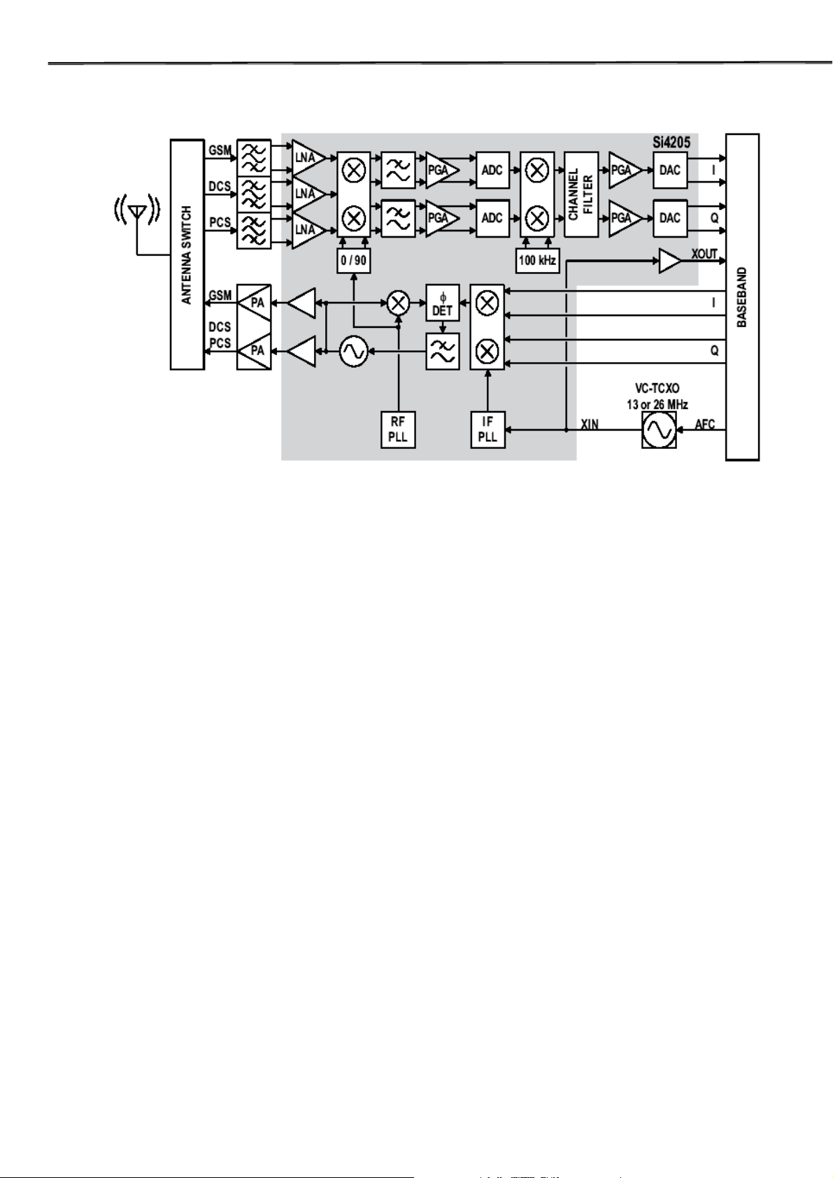
4.2 Radio Transceiver Section
Fig.4-1. RF Transceiver block diagram
The GF200’s RF Transceiver, which is AEROI(SI4205) transceiver is the industry’s most
integrated
RF front end for multi-band GSM/GPRS digital cellular handsets and wireless data modems.
The highly integrated solution eliminates the IF SAW filter, external low noise amplifiers (LNAs)
for three bands, transmit and RF voltage controlled oscillator (VCO) modules, and more than 70
other discrete components found in conventional designs. The receive section uses a digital low-IF
architecture that avoids the difficulties associated with direct conversion while delivering lower
solution cost and reduced complexity. The baseband interface is compatible with any supplier’s
baseband subsystem. The transmit section is a complete up-conversion path from the baseband
subsystem to the power amplifier, and uses an offset phase-locked loop (PLL) with a fully integrated
transmit VCO. The frequency synthesizer uses Silicon Laboratories’ proven technology, which
includes integrated RF and IF VCOs, varactors, and loop filters.The unique integer-N PLL
architecture produces a transient response that is superior in speed to fractional-N architectures
without suffering the high phase noise or spurious modulation effects often associated with those
designs. This fast transient response makes the AEROI(SI4205) transceiver well suited to GPRS
multi-slot applications where channel switching and settling times are critical.
The following Figure shows of RF Transceiver PCB Layout
14
PANTECH R&D CONFIDENTIAL
Page 16

GF200 Service Manual
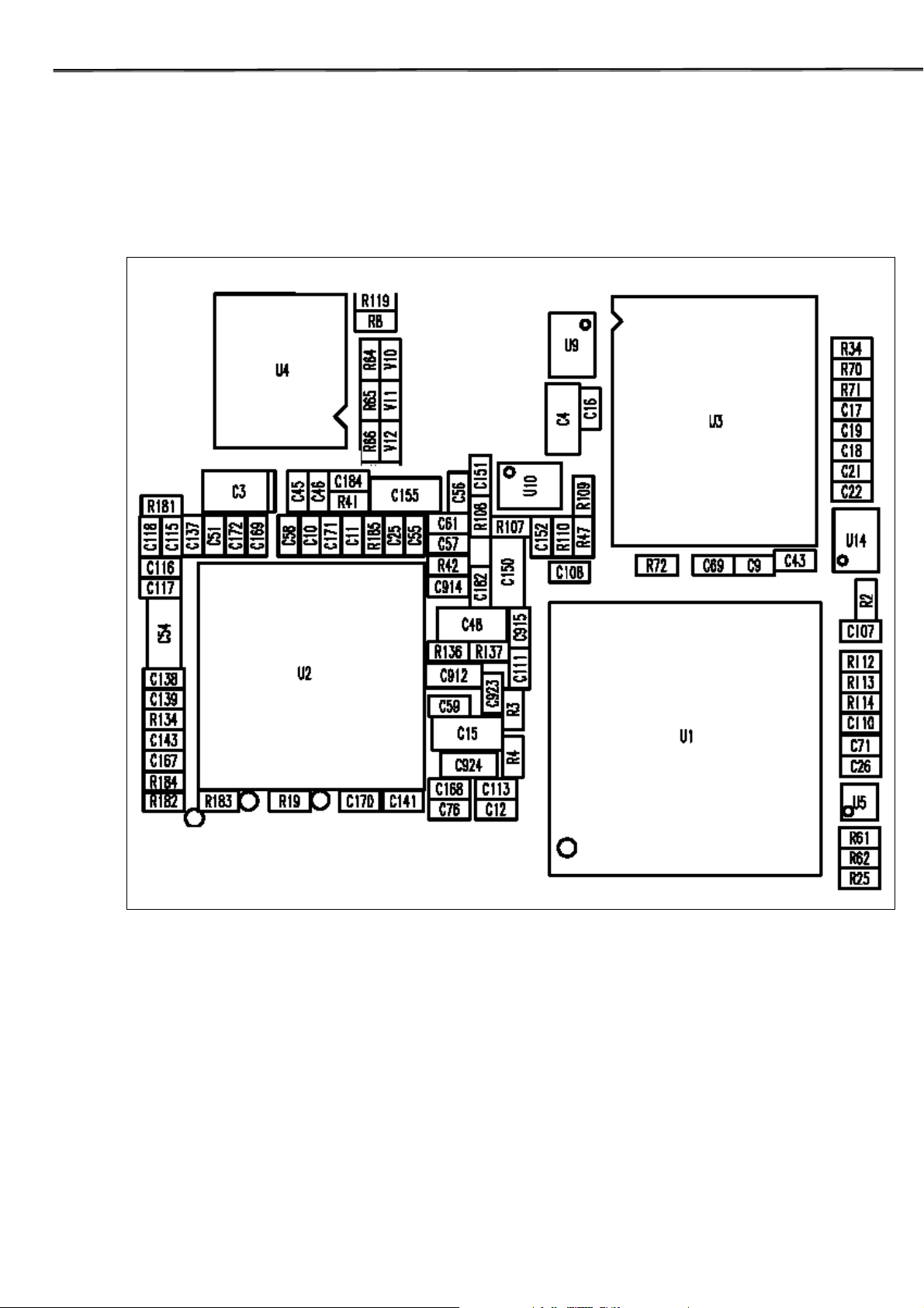
Fig.4-2. Top view of RF Transceiver PCB Layout
4.2.1 DC Distribution and Regulation Part
The battery voltage, in return, is applied to the logic part and RF part via LDO(Low Drop-Out)
regulator. As several LDO regulators are used, power can be supplied for each necessary part
efficiently. Audio/Logic parts use +2.8V. Si4205 RF Transceiver (U710) also use +2.8V DC voltage.
4.2.2 Transciever pin description
Fig.4-3. Top View of Si4205-BM
15
PANTECH R&D CONFIDENTIAL
Page 17

GF200 Service Manual
Table 4-1. Pin Description of Si4205-BM
16
PANTECH R&D CONFIDENTIAL
Page 18

GF200 Service Manual
4.2.3 Receiver Section
4.2.3.1 An Overview of Receive section
Fig.4-6. Receiver block diagram
GF200’s Aero I transceiver uses a low-IF receiver architecture which allows for the on-chip integration
of the channel selection filters, eliminating the external RF image reject filters and the IF SAW filter
required in conventional superheterodyne architectures. Compared to a direct-conversion architecture,
the low-IF architecture has a much greater degree of immunity to dc offsets, which can arise from RF
local oscillator (RFLO) self-mixing, 2nd-order distortion of blockers, and device 1/f noise. This relaxes
the common-mode balance requirements on the input SAW filters, and simplifies PC board design and
manufacturing.
Three differential-input LNAs are integrated on the Aero I transceiver. The GSM input supports the
GSM 850 (869–894 MHz) or EGSM 900 (925–960 MHz) bands. The DCS input supports the DCS 1800
(1805–1880 MHz) band. The PCS input supports the PCS 1900 (1930–1990 MHz) band.
The LNA inputs are matched to the 150 Ω balancedoutput SAW filters through external LC matching
networks. The LNA gain is controlled with the LNAG and LNAC bits.
A quadrature image-reject mixer downconverts the RF signal to a 100 kHz intermediate frequency (IF)
with the RFLO from the frequency synthesizer. The RFLO frequency is between 1737.8 to 1989.9 MHz,
and is internally divided by 2 for GSM 850 and E-GSM 900 modes. The mixer output is amplified with an
analog programmable gain amplifier (PGA), which is controlled with the AGAIN bits in register 05h. The
quadrature IF signal is digitized with high resolution A/D converters (ADCs).
The ADC output is downconverted to baseband with a digital 100 kHz quadrature LO signal. Digital
decimation and IIR filters perform channel selection to remove blocking and reference interference
signals. The response of the IIR filter is programmable to a high selectivity setting or a low selectivity
setting. The low selectivity filter has a flatter group delay response which may be desirable where the
17
PANTECH R&D CONFIDENTIAL
Page 19

GF200 Service Manual
final channelization filter is in the baseband chip. After channel selection, the digital output is scaled with
a digital PGA, which is controlled with the DGAIN bits.
The LNAG, LNAC, AGAIN and DGAIN bits must be set to provide a constant amplitude signal to the
baseband receive inputs.
DACs drive a differential analog signal onto the RXIP, RXIN, RXQP, and RXQN pins to interface to
standard analog-input baseband ICs. No special processing is required in the baseband for offset
compensation or extended dynamic range. The receive and transmit baseband I/Q pins can be
multiplexed together into a 4-wire interface. The common mode level at the receive I and Q outputs is
programmable, and the full scale level is also programmable.
4.2.3.2 Receiver Part
A. Antenna Swithch Module : Z701
SWITCHPLEXER consists of Tx filter, RX Dual SAW filter and having an antenna port, and dual
configuration with the transmitting path isolated from the receiving path. A signal receives from the
antenna of frequency band which is 942.5±17.5MHz for EGSM bands, 1842.5±37.5 MHz for DCS
bands and transmits it to dual saw filter. The Tx filter passes through the output signals of frequency
band that is 897.5MHz ±17.5MHz for EGSM bands, 1747.5 ±37.5 MHz for DCS bands from the
power amplifier and transmits it to the antenna. The maximum insertion loss is about 0.8 dB for the
receiving bands at 25
o
C and about 1.35 dB for the transmitting bands at 25o C.
Antenna
Swithch
Module
Matching Network
RF Transcever
Fig.4-7. Receiver part PCB Layout
18
PANTECH R&D CONFIDENTIAL
Page 20

GF200 Service Manual
4.2.4 Transmit Section
4.2.4.1 An Overview of Transmit Section
Fig.4-8. Transmitter block diagram
The transmit (TX) section consists of an I/Q baseband upconverter, an offset phase-locked loop
(OPLL) and two output buffers that can drive external power amplifiers (U701), one for the GSM 850
(824 to 849 MHz) and E-GSM 900 (880 to 915 MHz) bands and one for the DCS 1800 (1710 to 1785
MHz) and PCS 1900 (1850 to 1910 MHz) bands. The OPLL requires no external duplexer to
attenuate transmitter noise or spurious signals in the receive band, saving both cost and power.
Additionally, the output of the transmit VCO(TXVCO) is a constant-envelope signal that reduces the
problem of spectral spreading caused by non-linearity in the PA.
A quadrature mixer upconverts the differential in-phase (TXIP, TXIN) and quadrature (TXQP,
TXQN) signals with the IFLO to generate a SSB IF signal that is filtered and used as the reference
input to the OPLL. The IFLO frequency is generated between 766 and 896 MHz and internally
divided by 2 to generate the quadrature LO signals for the quadrature modulator, resulting in an IF
between 383 and 448 MHz. For the E-GSM 900 band, two different IFLO frequencies are required
for spur management. Therefore, the IF PLL must be programmed per channel in the E-GSM 900
band. The OPLL consists of a feedback mixer, a phase detector, a loop filter, and a fully integrated
TXVCO. The TXVCO is centered between the DCS 1800 and PCS 1900 bands, and its output is
divided by 2 for the GSM 850 and E-GSM 900 bands. The RFLO frequency is generated between
1272 and 1483 MHz. To allow a single VCO to be used for the RFLO, high-side injection is used for
the GSM 850 and E-GSM 900 bands, and low-side injection is used for the DCS 1800 and PCS
1900 bands. The I and Q signals are automatically swapped when switching bands. Additionally,
the SWAP bit in register 03h can be used to manually exchange the I and Q signals.
Low-pass filters before the OPLL phase detector reduce the harmonic content of the quadrature
modulator and feedback mixer outputs. The cutoff frequency of the filters is programmable.
19
PANTECH R&D CONFIDENTIAL
Page 21

GF200 Service Manual
4.2.4.2 Transmitter Part
A. 6dB attenuators : Z705, Z706
These passive components are adopted for PAM to operate in a stable output power.
B. ASM(Antenna Switch Module / built in LPF): Z701
These filters pass through the signals of which frequency band of 880~915MHz,
1710MHz~1785MHz and 1850MHz~1910MHz which is the transmit frequencies of GSM, DCS and
PCS1900 system terminal respectively, and it suppresses other images and spurious frequencies
when the terminal transmits GMSK modulated frequencies
C. Power AMP Module(PAM): U701
This device amplifies signals ahead of transmiting them through the antenna to provide a
sufficient RF power. It has amplification factor of 28dB and efficiency of about 55% typically in GSM
band and amplification of 27dB and efficiency of about 52% typically DCS/PCS band.
D. RF Switch connector: J701
RF Switch connector used to test Mainboard’s RF characteristics and to calibrate.
E. Antenna: Antenna Contact Plate J702
This device enables signals to be transmitted and received from BTS by Um interface.
External Antenna can be contacted with Mainboard through Antenna Contact Plate.
20
PANTECH R&D CONFIDENTIAL
Page 22

GF200 Service Manual
GF200 Service Manual
Antenna
Contact
Plate
Attenuator
6dB
PAM
Fig.4-9. Transmit part PCB Layout
21
21
PANTECH R&D CONFIDENTIAL
PANTECH R&D CONFIDENTIAL
Page 23

GF200 Service Manual
4.2.5 Offset PLL
4.2.5.1 An Overview of Offset PLL
Fig.4-10. Si4205 Frequency Synthesizer Block Diagram
The Aero I transceiver integrates two complete PLLs including VCOs, varactors, resonators, loop
filters, reference and VCO dividers, and phase detectors. The RF PLL uses two multiplexed VCOs.
The RF1 VCO is used for receive mode, and the RF2 VCO is used for transmit mode. The IF PLL is
used only during transmit mode. All VCO tuning inductors are also integrated.
The IF and RF output frequencies are set by programming the N-Divider registers, NRF1, NRF2
and NIF. Programming the N-Divider register for either RF1 or RF2 automatically selects the proper
VCO. The output frequency of each PLL is as follows:
fOUT= N×fφ
The DIV2 bit in register 31h controls a programmable divider at the XIN pin to allow either a 13 or 26
MHz reference frequency. For receive mode, the RF1 PLL phase detector update rate (fφ ) should
be programmed fφ = 100 kHz for DCS 1800 or PCS 1900 bands, and fφ = 200 kHz for GSM 850
and E-GSM 900 bands. For transmit mode, the RF2 and IF PLL phase detector update rates are
always fφ =200 kHz.
22
PANTECH R&D CONFIDENTIAL
Page 24

GF200 Service Manual
4.2.5.2 VC-TCXO(Voltage Controlled Temperature Compensated Crystal Oscillator): V801
This is the mobile station’s reference frequency source. Its frequency is 13MHz, this signal is
applied to Si4205(U710)_Pin8, AD6526(U1)_Pin L12 .
VCTCXO
Fig.4-11. Top view of VCTCXO part on the PCB artwork
23
PANTECH R&D CONFIDENTIAL
Page 25

GF200 Service Manual
Section 5. Alignment Procedure
5.1 Recommended Test Equipment
Model No. Description Maker Remark
E5515C
GSM Mobile Station
Test Set
Agilent Technologies
8593E Spectrum Analyzer Hewlett Packard
TDS 3054B Oscilloscope Tektronix
FLUKE 87 Digital Multimeter Fluke
E3630A DC Power Supply Hewlett Packard
Others Accessory
5.2 Connection of Test Equipment
8593E Spectrum Analyzer
Coupler
8960 Test Set
RS-232C
PHONE
Fig.5-1. Test Set Configuration
Interface Connectors
RF Connectors
Power Supply
24
PANTECH R&D CONFIDENTIAL
Page 26

GF200 Service Manual
SECTION 6. Equipment Repair Procedure
6.1 no power on with battery applied
6.1.1 Power CHECK
1. Check battery power : 3.5V~4.2V.
BATTERY PACK
Terminal
GND
2. Check to see if U2.C15 pin voltage is same with battery power : CP100
CP100
CP100
25
PANTECH R&D CONFIDENTIAL
Page 27

GF200 Service Manual
3. Check to see if Q1.5.6 pin is same with battery power : CP101
CP101
CP101
26
PANTECH R&D CONFIDENTIAL
Page 28

GF200 Service Manual
4. Check to see if U2. A4,B4.T2,T3,P1,N1,and T7 pin is 2.8V, 1.8V,1.8V and 1.8V : CP102
CP102
CP102
5. Check to see if U2.T14 pin becomes to 0V : CP103
Pressing “END” key to turn on equipment.
27
PANTECH R&D CONFIDENTIAL
CP103
Page 29

GF200 Service Manual
6.1.2 Oscillation CHECK
1. Check to see if U1. A3 and B3 pin is oscillated(32.768KHz) : CP104
NO Check R138 and then replace X1
CP104
CP104
2. Check to see if R1.1 pin Master Clock(13MHz). : CP105
NO Check C1.2 pin and then check the PCB pattern, soldering
CP105
CP105
28
PANTECH R&D CONFIDENTIAL
Page 30

GF200 Service Manual
6.1.3 KEYPAD LED Not in Operation
1. Check to see if R127 is around 2.8V (duty: 80%, 256Hz) : CP110
NO Check R127, Q3 and then replace those.
2. Check to see if R10,R24,R25,R61,R62,R63,R125,R126 are same with battery voltage : CP111
NO Check the PCB pattern between battery and the resistors.
NO Replace the resistors.
3. Check to see if D4~15, D17~20 are well operated by multimeter : CP112
NO Replace the LEDs.
CP110
CP111
CP112
CP110
29
PANTECH R&D CONFIDENTIAL
Page 31

GF200 Service Manual
CP112
6.1.4 Status LED
During Operating Mode
Status LED Should be blinking during Operating Mode(Melody, Folder open, games).
1. Check to see if Q4.2,5 pin and 5.2 pin voltage is around 2.8V : CP115
NO Replace the Transistor.
During Incoming Call Mode.
Status LED should be blinking during Incoming Call
1. Check to see if Q4,Q5 is well operated. : CP115
NO Replace the Transistor.
CP115
CP115
30
PANTECH R&D CONFIDENTIAL
Page 32

GF200 Service Manual
6.2 Audio Part ( Earpiece, Hands-free Earphone, Microphone, Hands-free Mic )
6.2.1 No receiving tone heard ( Ear-piece )
1. Check to see if U9.3 is 2.5V : CP116
2. Check to see if U10.1 is around 1.2V : CP117
Set to HP8922M to connect a call and then set to 1kHz.
3. Check to see if J6.1 is 0V : CP118
CP118
CP117
CP116
CP118
31
PANTECH R&D CONFIDENTIAL
Page 33

GF200 Service Manual
CP116
CP117
32
PANTECH R&D CONFIDENTIAL
Page 34

GF200 Service Manual
6.2.2 Side Tone Not transmitted (Mic.)
1. Check to see if Mic + pin is around 1.8V : CP125
NO Check that R102, R103, C181 and R104 is cold solder, broken, short to the other
PCB pattern or not
If you find out any defective part, you replace it.
Set to HP8922M to connect a call and then set to 1kHz with Echo audio mode.
2. Check U102.J10 (C132) pins for wave form : CP126
NO Replace MIC
6.2.3 Side Tone Not transmitted ( Hands-free Mic. )
Repeat 6-2-2 No receiving tone heard.( Hands-free Earphone ).
1. Check to see if U102. H10 (C130) pin is 2.5V : CP127
NO Check that R107, R108, C150 and C151 is cold solder, broken, short to the other
PCB pattern or not.
If you find out any defective part, you replace it.
Set to HP8922M to connect a call and then set to 1kHz with Echo audio mode.
3. Check U102. H10 (C130) pins for wave form : CP127
NO Replace Handsfree Mic:CP128
CP125
CP126
CP127
33
PANTECH R&D CONFIDENTIAL
Page 35

GF200 Service Manual
CP127
CP126
CP125
6.2.4 Hook Switch not working
1. Check to see if U10.5 pin is 2.8V : CP129
2. Check to see if U10.1 pin is around 0.12V during pressing Hook Switch : CP130
3. Check to see if U10.3 pin is around 0.21V : CP131
NO Check that R109 and R110 cold solder, broken, short to the other PCB pattern or not
If you find out any defect, you replace it
4. Check to see if U10.4 pin is around 0V, when you press Hook Switch : CP132
NO Check that U10 cold solder, broken, short to the other PCB pattern or not
If you find out any defect, you replace it
34
PANTECH R&D CONFIDENTIAL
Page 36

GF200 Service Manual
CP131
CP129
CP132
CP130
6.2.5 Melody not ringing
1. Check to see if U4.32, 7 pin is 2.8V : CP133
2. Check SPK_L,SPK_R for waveform : CP134
NO Replacd SPK
CP129
CP130
CP131
CP132
35
PANTECH R&D CONFIDENTIAL
Page 37

GF200 Service Manual
CP133
CP134
CP133
CP134
36
PANTECH R&D CONFIDENTIAL
Page 38

GF200 Service Manual
6.2.6 Vibrator not working
1. Check to see if Q2.1 pin is 2.8V : CP137
NO Check to see Q2 cold solder, broken, short to the other PCB pattern or not
If you find out any defect, you replace it
2. Check to see Q2.6 is same with battery power : CP138
NO Check to see Q2 and R21 cold solder, broken, short to the other PCB pattern or not
If you find out any defect, you replace it
3.Check to see Vibrator
If you find out any defect, you replace it
CP137
CP138
CP137
CP128
37
PANTECH R&D CONFIDENTIAL
Page 39

GF200 Service Manual
6.3 SIM card part
6.3.1 SIM error
1. Check to see if J3.1 pin is around 2.85V : CP140
If you find out any defect, you replace it
2.Check to see J3.2, 3, 6 for wave form : CP142
NO Check to see J3, R132 and C183 cold solder, broken, short to the other PCB pattern
or not
If you find out any defect, you replace it
CP140
CP142
CP140
CP142
38
PANTECH R&D CONFIDENTIAL
Page 40

GF200 Service Manual
6.4 Charger part
6.4.1 Charging error
Insert adaptor into I/O jack.
1. Check to see if U2.A5 pin is 5.2V : CP143
NO Check to see J1.23, 24 pin cold solder, broken, short to the other PCB pattern or not :
CP144
If you find out any defect, you replace it
2. Check to see U2.B5 pin is low (0V) : CP145
NO Check to see U2 cold solder, broken, short to the other PCB pattern or not
If you find out any defect, you replace it
3. Check to see Q1.5,6 pin(same as the pin U2.A7) is 4.2V : CP146
NO Check to see Q1, R135 cold solder, broken, short to the other PCB pattern
or not
If you find out any defect, you replace it
CP143
CP145
CP146
CP144
39
PANTECH R&D CONFIDENTIAL
Page 41

GF200 Service Manual
CP143
CP145
CP146
CP144
40
PANTECH R&D CONFIDENTIAL
Page 42

GF200 Service Manual
6.5 Camera Sensor Part
6.5.1 Camera Preview error
1. Check to see if IC1.3 pin(On LCD Module) is around 1.8V : CP142
NO replace the IC1
2. Check to see if IC2.3 pin(On LCD Module) is around 2.8V CP143
NO replace the IC2
3. Check to see if IC5.3 pin(On LCD Module) is around 2.5V CP144
NO replace the IC5
4. Check to see if R501.2 pin(On LCD Module) is oscillated(27Mhz): CP145
NO Replace the Crystal (X501)
5 .Check to see if U101.B2,C1 pin(On LCD Module) is oscillated(27Mhz): CP146
NO Replace the Crystal (X501 or U101)
CP142
CP143
41
PANTECH R&D CONFIDENTIAL
Page 43

GF200 Service Manual
CP144
CP145
CP146
42
PANTECH R&D CONFIDENTIAL
Page 44

GF200 Service Manual
6.6 RF Part
6.6.1 Test conditions
1. Test condition 1 : VBAT = 3.8V during all tests
2. Test condition 2 : Traffic channel :EGSM Band
Tx mode
Ch62
Power Level : 13
3. Test condition 3 : Traffic channel : DCS Band
Tx mode
Ch698
Power Level : 10
4. Test condition 4 : Traffic channel :GSM Band
Rx mode
Ch62
Input power : -70dBm
5. Test condition 5 : Traffic channel : DCS Band
Rx mode
Ch698
Input power : -70dBm
6. Test condition 5 : Traffic channel : PCS Band
Tx mode
Ch662
Input power : -70dBm
7. Test condition 6 : Traffic channel : Everything Test
VCTCXO 13MHz Referance Check
% RF power values are measured using 50Ωcoaxial cable.
43
PANTECH R&D CONFIDENTIAL
Page 45

GF200 Service Manual
6.6.2 Power Supply Check Point _ TEST CONDITION 1
Step
Te st
point
Typical Value Condition Checking Point
2-1
2-2
U907
Pin#1
3.8V 2, 3, 4, 5,6
Check route connection : VBAT
YES : Pass
NO : Power Supply Check
Check route connection : VCC_2.8V
YES : Pass
U907
Pin#5
2.8V 2, 3, 4, 5,6
NO 1: Step2-1 Check
NO 2: U907 Pin3 Check
Logic High : LDO Repair
Logic Low : Clock Check
(Test Condition 6)
LOGIC HIGH STEP 2-1
3 2 1
45
STEP 2-2
Fig.6-1 U907 Regulator Power Supply PCB Layout
44
PANTECH R&D CONFIDENTIAL
Page 46

GF200 Service Manual
Fig.6-2 U907 Regulator Power Supply Schematic
45
PANTECH R&D CONFIDENTIAL
Page 47

GF200 Service Manual
6.6.3 Power Amplifier Module _ TEST CONDITION 2,3,4,5
Step Test point Typical Value Condition Checking Point
Check route connection : VBAT
3-1
U701
Pin #4
3.8V 2,3,6
YES : Pass
NO : Power Suppely Check
Test Condition1 Check
3-2
3-3
U701
Pin #3
U701
Pin #2
LOGIC PULSE
_ 217HZ
2,3,6
Check route connection : PAM Enable
NO : U1 Repair
Check this pin #2, When Logic High, then
LOGIC 2,3,6
DCS/PCS Mode. While Logic Low , GSM
mode is operating.
YES : Pass
STEP 3-1
STEP 3-2
STEP 3-3
Fig.6-3. . Power Amp Module Test Point on the PCB LAYOUT
46
PANTECH R&D CONFIDENTIAL
Page 48

GF200 Service Manual
STEP 3-1
STEP 3-2
Fig.6-4. Power Amplifier’s Test Point on the schematic
47
PANTECH R&D CONFIDENTIAL
Page 49

GF200 Service Manual
6.6.4 VCTCXO _ TEST CONDITION 6
Step
Te st
point
Typical Value Condition Reaction to Abnormality
4-1
4-2
STEP 4-1
V801
Pin#1
V801
Pin#4
1.4V ±0.25V
2.8V
2, 3, 4, 5,
6
2, 3, 4, 5,
6
Check route connection : AFC
YES : Pass
NO : U 1
Check route connection : VTCXO
STEP 4-2
Fig.6-5. VCTCXO Check Point Circuit
2 1
STEP 4-2
3
4
STEP 4-1
Fig.6-6. VCTCXO Check Point on the PCB Layout
48
PANTECH R&D CONFIDENTIAL
Page 50

GF200 Service Manual
6.6.5 Antenna Switch Module
Step Test point Typical Value Condition Check point
When Pin#10 is Logic High and Pin#2
is Logic Low the mode is EGSM band.
During Pin#2 and Pin#4 are Logic
High and Pin#10 is Logic Low the
operating mode is DCS band.
When PCS band is on operating, Both
Pin#2 and Pin#4 logics are high.
5-1
5-2
5-3
Z701
Pin#10
Z701
Pin#2
Z701
Pin#4
2.6V 2
2.6V 3,6
2.6V 3,6
STEP 5-1
STEP 5-2
STEP 5-3
Fig. 6-7 Antenna Switch Module Circuit
STEP 5-2
Fig. 6-8 Antenna Switch Module PCB Layout
49
PANTECH R&D CONFIDENTIAL
 Loading...