

Page 1

GB100 Service Manual GB100
GB100 Service Manual
(GSM Cellular Phone)
Pantech Co., Ltd., Korea
September 1, 2004
For Use by Authorized Service/Maintenance Personal Only
Documents to Receive This Addendum:
st
1
Edition
GB100 Maintenance/Repair/Operating Manual
Page 2

GB100 Service Manual
CONTENTS
SECTION 1 INTRODUCTION .............................................................................................................3
1.1 INTRODUCTION ..............................................................................................................................3
1.2 FREQUENCY ALLOCATION AND ITS USE ...........................................................................................3
1.3 ITEM NAME AND USE......................................................................................................................4
1.4 CHARACTERISTICS.........................................................................................................................4
SECTION 2 ELECTRICAL SPECIFICATIONS....................................................................................5
2.1 GENERAL ......................................................................................................................................5
2.2 TRANSMITTER…………………………………………………………………………………………….5
2.3 RECEIVER…………………………………………………………………………………………………5
SECTION 3 OPERATION....................................................................................................................6
3.1 NAME OF EACH PART…..……………………………….…………………………………………………6
3.2.DISPLAY ..………………….…………………………….………………………………………………..7
3.3 KEYPAD …………………………………….………….………………………………………………..7
SECTION 4 THEORY OF OPERATION..............................................................................................8
4.1 LOGIC SECTION........................................................................................................................8
4.1.1 DC DISTRIBUTION AND REGULATION PART…………………………………………………………….8
4.1.2 LOGIC PART…………………………………………………………………………………………….8
4.1.2.1 SUMMARY…………………………………………………………………………………………….8
4.1.2.2 BASEBAND DIGITAL SIGNAL PROCESSING…………………………………………………………..8
4.1.3 MEMORY PART………………………………………………………………………………………..10
4.1.4 NOTIFICATION PART .................................................................................................................. 11
4.1.5 KEY PAD PART.......................................................................................................................... 11
4.1.6 LCD MODULE(DISPLAY PART)................................................................................................... 11
4.2 RADIO TRANSCEIVER SECTION.....................................................................................................12
4.2.1 DC DISTRIBUTION AND REGULATION PART .................................................................................13
4.2.2 TRANSCEIVER PIN DESCRIPTION…………………………………………………….……….14
4.2.3 RECEIVE SECTION………………………………………………………………………………….…17
4.2.3.1 AN OVERVIEW OF RECEIVE SECTION.......................................................................................17
4.2.3.2 RECEIVER PART……………………………………………………………………………….……18
4.2.4 TRANSMIT SECTION ..................................................................................................................19
4.2.4.1 AN OVERVIEW OF TRANSMIT SECTION ....................................................................................19
4.2.4.2 TRANSMITTER PART...............................................................................................................20
4.2.5 OFFSET PLL……………………………………………………………………………….…………..21
4.2.5.1 AN OVERVIEW OF OFFSET PLL............................................................................................21
4.2.5.2 VCTCXO(VOLTAGE CONTROLLED TEMPERATURE COMPENSATED CRYSTAL OSCILLATOR):V801….22
SECTION 5 ALIGNMENT PROCEDURE..........................................................................................23
5.1 RECOMMENDED TEST EQUIPMENT................................................................................................23
5.2 CONNECTION OF TEST EQUIPMENT...............................................................................................23
SECTION 6 EQUIPMENT REPAIR PROCEDURE...........................................................................24
6.1 NO POWER ON WITH BATTERY APPLIED ..........................................................................................24
6.1.1 POWER CHECK.........................................................................................................................24
6.1.2 OSCILLATION CHECK ................................................................................................................30
6.1.3 KEYPAD LED NOT IN OPERATION(3-COLOR AND BLUE) ..............................................................31
6.1.4 LCD EL BACKLIGHT LED NOT IN OPERATION(WHITE)..………………………………………… …33
6.2 AUDIO PART(EARPIECE, HANDS FREE EARPHONE, MICROPHONE, HANDS FREE MIC) ..................35
6.2.1 NO RECEIVING TONE HEARD (EARPIECE) ..................................................................................35
6.2.2 NO RECEIVING TONE HEARD (HANDS FREE EARPHONE).............................................................35
6.2.3 SIDETONE NOT TRANSMITTED (EARPIECE)................................................................................38
6.2.4 SIDETONE NOT TRANSMITTED (HANDS FREE MIC) .....................................................................38
6.2.5 HOOK SWITCH NOT WORKING ..................................................................................................39
6.2.6 MELODY NOT RINGING.............................................................................................................40
1
PANTECH R&D CONFIDENTIAL
Page 3

GB100 Service Manual
6.2.7 VIBRATOR NOT WORKING …………………………………………………………………...…41
6.3 SIM CARD PART ……………………………………...…………………………………………….42
6.3.1 SIM ERROR ………………………………………………………………………………………….42
6.4 CHARGER PART……………………………………………………………………………………..43
6.4.1 CHARGING ERROR ………………………………..…………………………………………………43
6.5 RF PART…………….………………………………………………………………………………… 45
6.5.1 TEST CONDITIONS………………………………………………………………… …………………45
6.5.2 POWER SUPPLY CHECK POINT……………………………………………………………………….46
6.5.3 POWER AMPLIFIER MODULE ………………………………………………………………………...48
6.5.4 VCTCXO...…………...………………………………………………………………………………..50
6.5.5 ANTENNA SWITCH MODULE……………………………………………………….…………………..51
2
PANTECH R&D CONFIDENTIAL
Page 4

GB100 Service Manual
SECTION 1. Introduction
1.1 An Introduction of GSM Digital Cellular Mobile Communication System
GSM (Global System for Mobile communication) concluded that digital technology working in
the Time Division Multiple Access (TDMA) mode would provide the optimum solution for the
future system. Specifically , a TDMA system has the following advantage
► Offers a possibility of channel splitting and advanced speech coding ,resulting in improved
spectrum efficiency.
► Offers much greater variety of service than the analog
► Allows considerable improvements to be made with regards to the protection of information.
The GSM system is basically designed as a combination of three major subsystem;
The network subsystem, the radio subsystem, and the operation support system.
The functional architecture of a GSM system can be divided into the Mobile Station (MS), the Base
Station (BS), and the Network Subsystem (NS). The MS is carried by the subscriber, the BS
subsystem controls the radio link with the MS and the NS performs the switching of calls between
the mobile and other fixed or mobile network users as well as mobility management. The MS and
the BS subsystem communicate across the Um interface also known as radio link
The specifications relating to MS are as follows:
z TS 100 607-1 : Digital cellular telecommunication system(Phase2+)Mobile Station (MS) con
Formance specification Part1:Conformance specification
1.2 Frequency Allocation and Its Use
z Transmit frequency band : 880 MHz ~ 915 MHz(For EGSM), 1710 MHz ~ 1785 MHz(For DCS)
1850 MHz ~ 1910 MHz(For PCS)
z Receive frequency band: 925 MHz ~ 960 MHz(For EGSM) , 1805 MHz ~ 1880 MHz(For DCS),
1930 MHz ~ 1990 MHz(For PCS)
z Channel spacing : 200 KHz
z ARFCN(Absolute Radio Frequency Channel Number) : 1~124 and 975~1023 (For EGSM),
512~885 (For DCS), 512~810 (For PCS)
z Transmit·receive frequency spacing: 45 MHz(For EGSM),
z Frequency band and Channel Arrangement
For standard GSM Fl(n)=890+0.2*n 1 ≤n≤ 124 Fu(n)=Fl(n)+45
890 MHz ~915 MHz : Mobile Transmit,Base receive
935 MHz ~960 MHz : Base Transmit, Mobile receive
For Extended GSM Fl(n)=890+0.2*n 1 ≤n≤ 124 Fu(n)=Fl(n)+45
Fl(n)=890+0.2*(n-1024) 975 ≤n≤ 1023
880 MHz ~915 MHz : Mobile Transmit,Base receive
95MHz(For DCS), 80MHz(For PCS)
925 MHz ~960 MHz : Base Transmit, Mobile receive
For DCS Fl(n)=1710.2+0.2*(n-512) 512≤n≤885 Fu(n)=Fl(n)+95
1710 MHz ~ 1785 MHz : Mobile Transmit,Base receive
3
PANTECH R&D CONFIDENTIAL
Page 5

GB100 Service Manual
1805 MHz ~ 1880 MHz : Base Transmit, Mobile receive
For PCS Fl(n)=1850.2+0.2*(n-512) 512 ≤n≤ 810 Fu(n)=Fl(n)+80
1850 MHz ~1910 MHz : Mobile Transmit,Base receive
1930 MHz ~1990 MHz : Base Transmit, Mobile receive
** Fl(n)= frequency value of the carrier , Fu(n)= corresponding frequency value in upper band
1.3 Item Name and Usage
GB100, GSM digital cell phone, is supercompact, superlight mobile communication terminal for
personal use. It has a 900MHz, 1800MHz and 1900MHz frequency band and adopts GSM and
PCS mode having excellent spectrum efficiency, economy, and portability.
This product is GSM Cellular type portable phone, adopting 1-cell Li-ion battery and power saving
circuit to maximize its operation time. Also, it is equipped with a fixed antenna (snap-in type) and its
color LCD with font built in enables both Chinese and English text service. And power control(basic
feature of GSM), security feature, voice symbol feature, and variable data rate feature are used
appropriately to ensure its best performance. This product consists of a handset, battery pack, and
Travel charger.
1.4 Characteristics
1) All the active devices of GB100 are made of semiconductors to ensure excellent performance
and semi-permanent use.
2) Surface mounting device (SMD) is used to ensure high reliability, compactness and lightness.
3) GB100 adopts the Skyworks’s RF transceiver, which is CMOS RF front-end for multi-band GSM
digital cellular handsets. The Skyworks’s RF transceiver highly-integrated architecture
eliminates the IF SAW filter, low noise amplifiers (LNAs) for three bands, transmit and RF
voltage-controlled oscillator (VCO) modules, and more than 60 other discrete components found
in conventional GSM handsets to deliver smaller, more cost effective GSM solutions that are
easier to design and manufacture.
4) GB100 is designed to perform excellently even in the worst environment
4
PANTECH R&D CONFIDENTIAL
Page 6
GB100 Service Manual
Section 2. Electrical Specifications
2.1 General E-GSM / PCS Band
Mobile Transmit Frequency
Mobile Receive Frequency
The Number of Time Slot 8
The Number of Channels 174 / 374 / 299
Channel Spacing 200 kHz
Power Supply Rechargeable Li-Ion Battery 3.7V/680mAh
Operating Temperature
Dimension
Weight 76 g
880 MHz ~ 915 MHz / 1710 MHz ~1785 MHz / 1850MHz ~
1910MHz
925 MHz ~ 960 MHz / 1805 MHz ~ 1880 MHz / 1930MHz
~1990MHz
-10℃ ∼ +55℃
76(H) ×40(W) ×23.5(D) mm (SLIM)
2.2 Transmitter E-GSM / PCS Band
Maximum Output Power
Frequency Error
Phase Error
Minimum Output Power
Power Control
Output RF Spectrum TS 100 910V6.2.0
Switching Transient TS 100 910V6.2.0
Intermodulation attenuation
EGSM and DCS
Allocated a channel;
-36dBm 9kHz ~ 1GHz
-30dBm 1GHz ~ 12.75GHz
Idle mode;
-57dBm 9KHz ~ 1GHz
-47dBm 1GHz ~ 12.75GHz
with the following excoptions
-59dBm 880MHz ~ 915MHz
Conducted Spurious Emissions
-53dBm 1.71GHz ~ 1.785GHz
-76dBm 1900 ~ 1920MHz, 1920 ~ 1980MHz, 2010 ~
PCS
Allocated Channel;
-36dBm 9KHz~ 1GHz
-30dBm 1GHz~ 12.75GHz
Idle mode;
-57dbm 9kHz ~ 1000MHz
-53dBm 1850MHz ~ 1910MHz
-47dBm 1GHz ~ 12.75GHz
33±2 / 30±2 / 30±2 dBm
±90Hz / ±180Hz / ±180Hz
RMS < 5°, PEAK < 20°
5±5 / 0±5 dBm / 0±5 dBm
5~19(2 dB Step) ) / 0~15(2 dB Step) /
0~15(2 dB Step)
2025MHz, 2210 ~ 2170MHz
5
PANTECH R&D CONFIDENTIAL
Page 7
GB100 Service Manual
2.3 Receiver
For GSM900 small MS :-102dBm Reference Sensitivity
For Adjacent interference
For Adjacent(200KHz) interference
For Adjacent(400KHz) interference
For Adjacent(600KHz) interference
Section 3 Operation
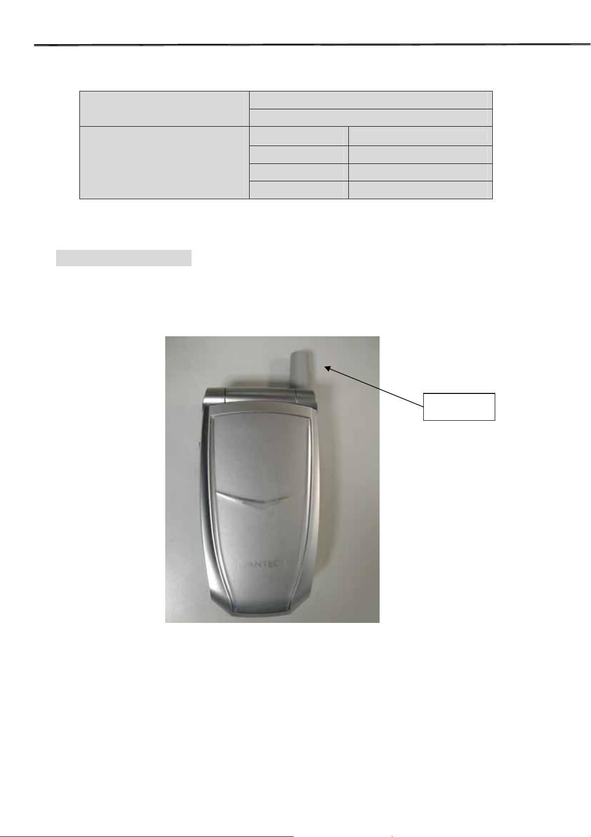
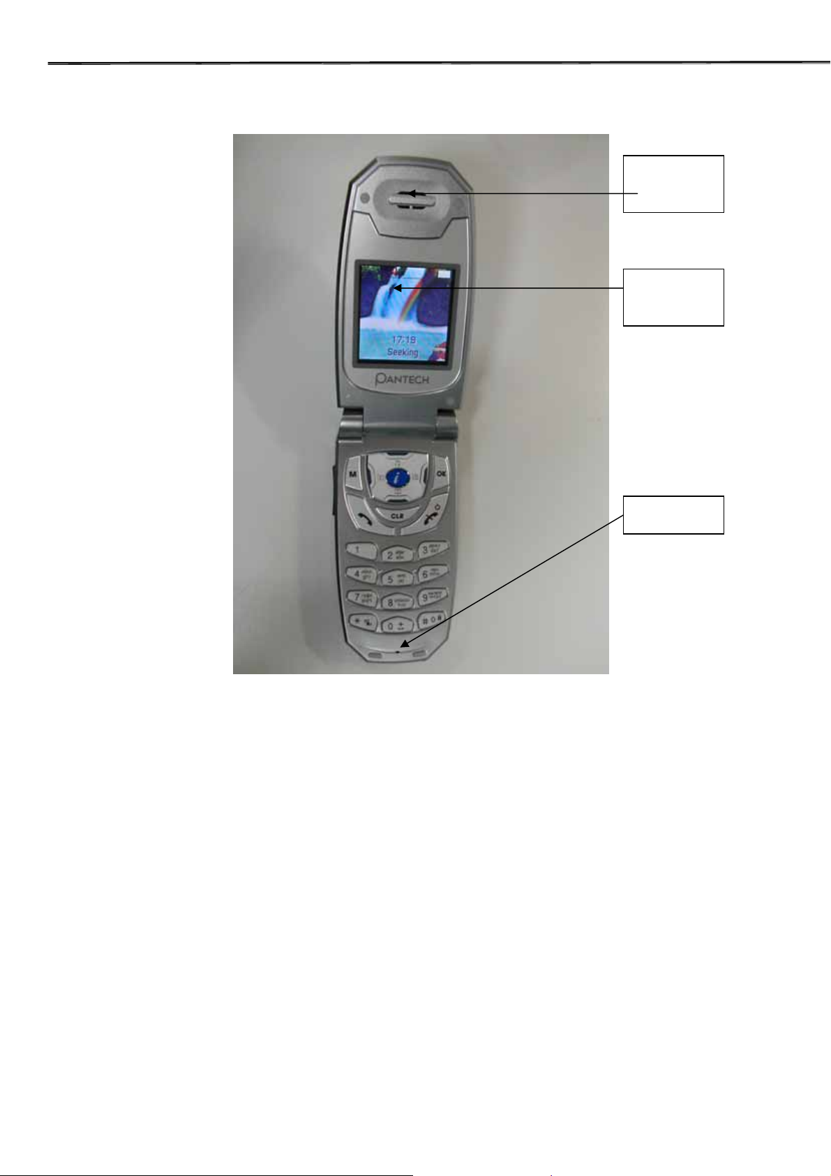
3.1 Name of each part
For DCS1800 / PCS1900 class3 MS : -102dBm
C/Ic
C/Ia1 -9 dB
C/Ia2 -41 dB
C/Ia3 -49 dB
9 dB
Antenna
6
PANTECH R&D CONFIDENTIAL
Page 8
GB100 Service Manual
Two-mode
Speaker
Display
Screen
Mic
7
PANTECH R&D CONFIDENTIAL
Page 9

GB100 Service Manual
3.2 Display(Single LCD)
Parameter Projected Actual (MAIN LCD)
Display Color STN LCD with white LED back lighting
65,000 colors
European Character
: (font size : 16×16) 7 lines x 8 characters
Chinese Character
: (font size : 16×16) 7 lines × 8 characters
Driver HCD667A66UBP
Module Dimen. 34.8(W) x 41.61(H) x 4.94(D)
Active Area 28.868(W) x 28.868(H)
Dot pitch 0.07(W) x 0.21(H)
3.3 Keypad
Market Goal Projected Actual Comments
English
Keypad
0-9, *,#
Send (Color)
End/Pwr (Color)
Up (Melody),
Down (Phonebook),
Left (My menu),
Right (SMS)
Center (WAP)
MENU, OK, CLR
* Key: Vib. Mode
# Key: Auto Lock
0/+Key:
International
0-9, *,#
Send (Color)
End/Pwr (Color)
Up (Melody),
Down (Phonebook),
Left (My menu),
Right (SMS)
Center (WAP)
MENU, OK, CLR
* Key: Vib. Mode
# Key: Auto Lock
0/+Key: International
2 Volume Keys
Meets Goal.
(Industrial design
sample required)
Meets Goal
Keys for VR and
Lock
International
Volume up/down
2 Volume Keys
8
PANTECH R&D CONFIDENTIAL
Page 10

GB100 Service Manual
Section 4. Theory of Operation
4.1 Logic Section
4.1.1 DC Distribution and Regulation Part
Applying battery voltage and pressing “END” key on the key pad short-circuits “Ground” and “
PowerON”. AD6535(U102) control that power manage regarding power on/off in handset
Pressing POWERKEY on the key pad is active on the handset.
This will turn on all the LDOs, when PowerON is held low. The power of RF Tx power amplifier is
supplied directly by the battery.
4.1.2 Logic part
4.1.2.1 Summary
The logic part consists of AD6525 ARM7 microprocessor-combined DBB(Digital BaseBand)
GSM-ASIC, COMBO(flash ROM & SRAM), AD6535 ABB(Analog BaseBand) Chip. AD6525 is
GSM-ASIC chipset implemented for GSM terminal’s system control and baseband digital signal
processing.
Major parts used in the logic part are as follows:
1) AD6525 : U101, [ARM7 Processor Core + DBB GSM Signal Processing] ASIC
2) AD6535 : U102, Analog Baseband Processor (Power management + Voice Codec)
3) COMBO MEMORY(Flash ROM : U1, 64Mbit Flash Memory + 16Mbit SRAM )
4.1.2.2 Baseband Digital Signal Processing
AD6525 is a GSM core device containing ARM7 CPU core. AD6525 is 160 pin LFBGA (mini-BGA)
package, consisting of terminal chips. The function and characteristics of clock are as follows:
1) Complete single chip GSM Processor
2) Channel codec sub-system
• Channel coder and decoder
• Interleaver and Deinterleaver
• Encryption and Decryption
3) Control Processor Subsystem including
• Parallel and serial Display interface
• Keypad Interface
• SIM Interface
• Control of RADIO subsystem
• Real Time Clock with Alarm
PANTECH R&D CONFIDENTIAL
9
Page 11

GB100 Service Manual
☞ Configuration by Function of AD6525
1 Microprocessor Core
AD6525 has a built-in ARM7 microprocessor core, including microprocessor interrupt controller,
timer/counter, and DMA controller. And besides, 32bit data path is included, and up to 8Mbyte
addressing is enabled and can be extended up to 16Mbyte. Although external clock should be
provided to operate the microprocessor, this core uses 13MHz VCTCXO to provide clock.
2 Input Clock
1) Main Clock(13 MHz):
This is the clock needed for the microprocessor built in AD6525 to operate.
2) VC-TCXO(13 MHz) , 32.768KHz Clock:
This is the system reference clock to control SLEEP mode.
This is the clock derived from 13MHz VC-TCXO clock, provided by RF part. It is the timing
reference clock for GSM signal processing.
3 DSP Subsystem
This is a GSM signal processing part in GSM mode, consisting of speech transcoding and
Channel equalization as follows:
1) Speech transcoding
In full rate, the DSP receives the speech data stream from VBC and encodes data from 104kbps to
13kbps. Using algorithm is Regular Pulse Excitation with Long Term Prediction (RPE-LTP).
2) Equalization
The Equalizer recovers and demodulates the received signal
The Equalizer establishes local timing and frequency references for mobile terminal as well as
RSSI calculation.
The equlization algorithm is a version of Maximum Likelihood Sequency Estimation(MLSI)
using Viterbi Algorithm.
☞ GSM Core and RF Interface
1) Transmitter:
AD6535 ABB receive data at 270kbps and use an on chip lock-up table to perform GMSK
modulation. A pair of 10bit matched differential DACs convert the modulated data and pass
I and Q analog data to the transmit section of the radio system.
2) Receiver:
The receiver I and Q signals are sampled by a pair of ADCs at 270kbps.
The I and Q samples are transferred to the EGSMP through a dedicated receive path serial port.
4 RF Interface
10
PANTECH R&D CONFIDENTIAL
Page 12

GB100 Service Manual
This interfaces the RF part to control power amplifier, Tx LO buffer amplifier, VC-TCXO, and
AGC-end on transmit/receive paths in the RF part.
1) Transmitter Interface:
This transmits TX_AGC signal to Tx AGC amplifier to adjust transmit power level and sends
Ramp_DAC signal to the RF part to control power amplifier.
2) Receiver Interface:
This transmits RX_AGC signal to Rx AGC amp. to adjust receive path gain.
5 General Purpose ADC Support
The AD6535 includes a general purpose 10bit auxiliary ADC with four multiplexed input channel
These are used for measurment of battery voltage ID , temperature and accessory ID.
6 USC(Universal System Connector) Interface
A Typical GSM handset requires serial connections to provide data during normal phone operation
manufacturing,testing and debugging.
7 General Purpose Interface
The AD6525 provides 32 interface pin for control of peripheral devices.
All GPIO pins start up as inputs. Additional purpose inputs and outputs are available under SW
control.
8 Speech Transcoding
In full rate mode, the DSP receive the speech data stream from the ABB and encodes data from
104kbps to 13kbps.Using algorithm is Regular Pulse Exitation with Long Term Prediction as
specified GSM Recommandation
9 Power Down Control Section
1) Idle Mode Control:
If IDLE/ signal turns ‘Low’, transmitter section becomes disabled.
2) Sleep Mode Control:
If IDLE/ and SLEEP/ signals turn ‘Low’, all the sections except for VC-TCXO circuit become
disabled.
3) Receiver & Transmitter Mode Control:
If IDLE/ and SLEEP/ signals turn ‘High’, all the sections become enabled to perform
transmit/receive operation.
4.1.3 Memory Part
Memory consists of COMBO (flash ROM & SRAM).
1 Flash ROM
Flash ROM has a capacity of 64Mbit(8MByte). The main programs of the terminal(call processing,
user interface, and diagnostic task) and supplemental programs (NAM program and test program)
are stored in the flash ROM. Even if the program version may be changed in the future, customers
can download the program.
2 Static RAM
11
PANTECH R&D CONFIDENTIAL
Page 13

GB100 Service Manual
SRAM has a capacity of 16Mbit(2MByte) and stores system parameters, data buffer, and stack of
each task in it.
3 Key Tone Generation
All alert signals are generated by melody IC output.
4.1.4 Notification Part
The notification of incoming call is given by melody, vibrator, and 7color-LED.
1) Melody:
This is a device sounding alert/melody tones.
The melody datas are stored in flash memory (U104) And generated by 6525 DBB internal DSP.
2) Vibrator:
This is a device enabling vibration. The vibrator data is stored in flash memory(U104)
And generated by C5(GPO_23)pin.
3) 7color-LED:
This is a device to indicate a notification mode using the lamp.
U101 Nos. H12, C9 and B8 signal drives the lamp to flash.
4.1.5 Key Pad Part
To enable key operation to input information, the key matrix is configured using strobe signal of
KEYPADROW(0-4) and 5 input ports of KEYPADCOL(0-4). Also, to use the key even at light, the
backlight circuit is provided for LED 6s.
4.1.6 LCD Module(Display Part)
LCD module consists of LCD, controller, LED-Backlight,
LCD: 1S/W Icon x 1 lines[(128x3)x128] can be displayed on the LCD panel. 6 icons could be
provided by S/W. Controller with English font built in has been used.
LED-backlight Using illuminates the LCD panel, and LCD reflector enhances LCD display effect.
12
PANTECH R&D CONFIDENTIAL
Page 14
GB100 Service Manual
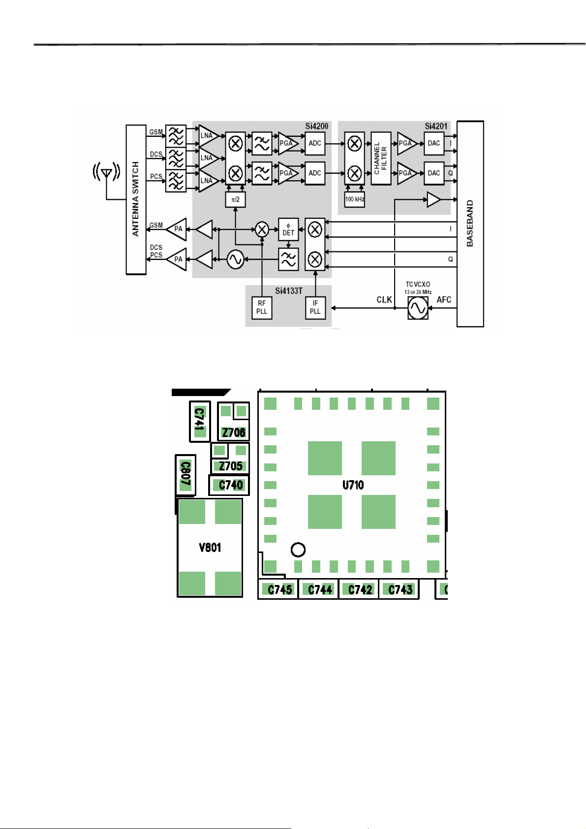
4.2 Radio Transceiver Section
Fig.4-1. RF Transceiver block diagram
Fig.4-2. Top view of RF Transceiver PCB Layout
The RF Transceiver of GB100, which is AERO I , consists of the GSM transimitter, the GSM
Receiver, and the RF synthesizer. The highly integrated solution eliminates the IF SAW filter,
external low noise amplifiers (LNAs) for three bands,
transmit and RF voltage controlled oscillator
(VCO) modules, and more than 60 other discrete components found in conventional designs.
The receive section uses a digital low-IF architecture that avoids the difficulties associated with
13
PANTECH R&D CONFIDENTIAL
Page 15
GB100 Service Manual
direct conversion while delivering lower solution cost and reduced complexity. The transmit section
is a complete up-conversion path from the baseband subsystem to the power amplifer (U701) and
uses an offset phase locked loop (PLL) with a fully integrated transmit VCO.
The frequency synthesizer includes integrated RF and IF VCO’s, Varactors, and Loop filters. The
unique integer-N PLL architecture produces a transient response that is superior in speed to
fractional architectures without suffering the high phase noise or spurious modulation effects often
associated with those designs.
4.2.1 DC Distribution and Regulation Part
The battery voltage, in return, is applied to the logic part and RF part via LDO(Low Drop-Out) regulator.
As several LDO regulators are used, power can be supplied for each necessary part efficiently.
Audio/Logic parts use +2.8V. SI4205 RF Transceiver(U501) and RF3133 Power Amplifer(U701) also
use +2.8V DC voltage.
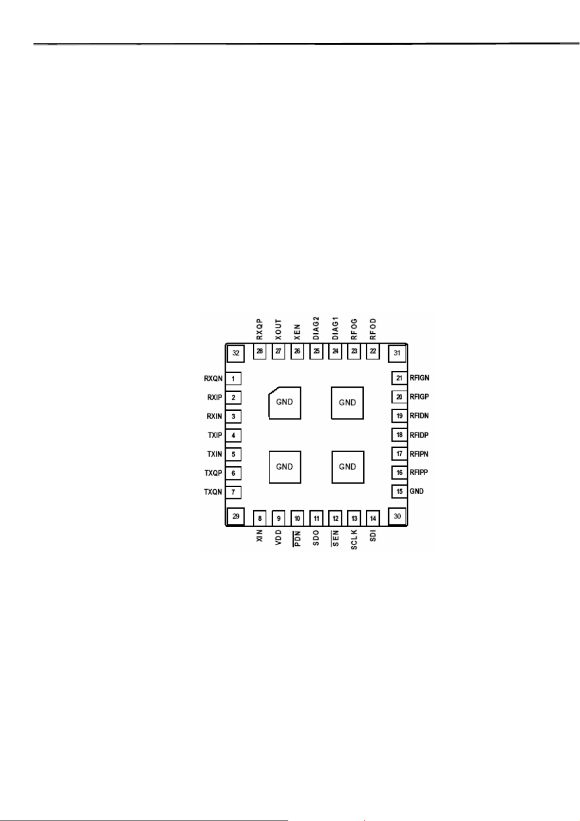
4.2.2 Transciever pin description
Fig.4-3. Top View of Si4205
14
PANTECH R&D CONFIDENTIAL
Page 16

GB100 Service Manual
Table 4-1. Pin Description of Si4205-BM
4.2.3 Receiver Section
4.2.3.1 An Overview of Receive section
Fig.4-6. Receiver block diagram
The GB100 model’s Aero transceiver uses a low-IF receiver architecture that follows for the
on-chip integration of the channel selection filters, eliminating the external RF image reject filters
15
PANTECH R&D CONFIDENTIAL
Page 17

GB100 Service Manual
and the IF SAW filter required in conventional superheterodyne architectures. Compared to a direct
conversion architecture, the low-IF architecture has a much greater degree of immunity to dc
nd
offsets that can arise from RF local oscillator (RFLO) self-mixing, 2
order distortion of blockers,
and device 1/f noise. This relaxes the common-mode balance requirements on the input SAW filters
and simplifies PC board design and manufacturing.
Three differential-input LNAs are integrated on the Aero I transceiver. The GSM input supports
EGSM 900 (925– 960 MHz) band. The DCS input supports the DCS 1800 (1805 – 1880 MHz).
A quadrature image-reject mixer downconverts the RF signal to a 100 kHz intermediate frequency
(IF) with the RFLO from the Si4133T frequency synthesizer. The RFLO frequency is between
1737.8 and 1989.9 MHz, and is divided by two in the Si4200 for GSM 850 and EGSM 900 modes.
The mixer output is amplified with an analog programmable gain amplifer (PGA), which is controlled
with the AGAIN[2:0] bits in register 05h. The quadrature IF signal is digitized with high resolution
A/D converters (ADCs).
ADC output is downconverted to baseband with a digital 100 kHz quadrature LO signal. Digital
decimation and IIR filters perform channel selection to remove blocking and reference interference
signals. After channel selection, the digital output is scaled with a digital PGA, which is controlled
with the DGAIN[5:0] bits in register 05h.
These analog and digital gain resigters must be set to provide a constant amplitude signal to the
baseband receive inputs.
DACs drive a differential analog signal onto the RXIP,RXIN,RXQP and RXQN pins to interface to
standard analog-input baseband Ics
4.2.3.2 Receiver Part
A. Diplexer: Z702
Diplexer consists of Tx filter, having an antenna port, and dual configuration with the transmitting
path isolated from the receiving path. A signal receives from the antenna of frequency band which
is 942.5±17.5MHz for EGSM bands, 1842.5±37.5 MHz for DCS bands and transmits it to dual saw
filter. The Tx filter passes through the output signals of frequency band that is 897.5MHz ±17.5MHz
for EGSM bands, 1747.5 ±37.5 MHz for DCS bands from the power amplifier and transmits it to the
o
antenna. The maximum insertion loss is about 0.8 dB for the receiving bands at 25
1.35 dB for the transmitting bands at 25
o
C.
B. SAW filter (BPF / Band select filter): U502, U503,U504
The U502 filter is for the EGSM band signals which range 942.5±17.5MHz with low insertion loss.
C and about
And the U503 filter passes the DCS bands that cover 1842.5 ±37.5MHz, the U504 filter passes the
PCS bands that cover 1960±30MHz.
These filters degrade other band signals with high passing loss of 30~60 dB. The EGSM and
DCSand PCS’s maximum insertion loss is 3.5 dB.
16
PANTECH R&D CONFIDENTIAL
Page 18

GB100 Service Manual
Fig.4-7. Receiver part PCB Layout
17
PANTECH R&D CONFIDENTIAL
Page 19

GB100 Service Manual
4.2.4 Transmit Section
4.2.4.1 An Overview of Transmit Section
Fig.4-8. Transmitter block diagram
The transmit (TX) section consists of an I/Q baseband upconverter, an offset phase-locked loop
(OPLL) and two 50 ohms output buffers that can drive external power amplifiers (PA), one for the
EGSM 900 (880 – 915 MHz) bands and others for the DCS 1800 (1710 – 1785 MHz) bands and
PCS1900(1850 – 1910MHz). The OPLL requires no external duplexer to attenuate transmitter noise
and spurious signals in the receive band, saving both cost and power. Additionally, the output of the
transmit VCO (TXVCO) is a constant-envelope signal which reduces the problem of spectral
spreading caused by nonlinearity in the PA.
A quadrature mixer upconverts the differential in-phase (TXIP,TXIN) and quadrature(TXQP,TXQN)
signals with the IFLO to generate a SSB IF signal which is fitered and usesd as the reference input
to the OPLL. The Si4133T generates the IFLO frequency between 766 and 896 MHz. The IFLO is
divided by two to generate the quadrature LO signals for the quadrature modulator, resulting in an IF
between 383 and 448 MHz.
The OPLL consists of a feedback mixer, a phase detector, a loop filter, and a fully integrated
TXVCO. The TXVCO is centered between the DCS 1800 and PCS 1900 bands, and its output is
divided by two for the generate the RFLO frequency between 1272 and 1483 MHz. To allow a single
VCO to be used for the RFLO, high-side injection is used for the EGSM 900 bands, and low-side
injection is used for the DCS 1800 and PCS 1900 bands. The I and Q signals are automatically
swapped when switching bands.
Low-pass fitlers before the OPLL phase detector reduce the harmonic content of the quadrature
modulator and feedback mixer outputs. The cutoff frequency of the filters is programmable.
18
PANTECH R&D CONFIDENTIAL
Page 20

GB100 Service Manual
4.2.4.2 Transmitter Part
A. 6 dB attenuator : Z705, Z706
These passive components are used for PAM to operate in a stable output power.
B. ASM(Antenna Switch Module / built in LPF): Z702
These filters pass through the signals of which frequency band of 880~915MHz,
1710MHz~1785MHz,1930MHz~1990MHz which is the transmit frequency of GSM, DCS, PCS
system terminal, and it suppresses other images and spurious frequencies when the terminal
transmits GMSK modulated frequencies.
C. Power AMP Module(PAM): U701
This device amplifies signals ahead of transmiting them through the antenna to provide a
sufficient RF power. It has amplification factor of 28dB and efficiency of about 55% typically in GSM
band and amplification of 27dB and efficiency of about 52% typically DCS and PCS band,
D. RF Switch connector: J701
RF Swithc connector used to test Mainboard’s RF characteristics.
E. Antenna: Antenna Contact Plate ; J702
This device enables signals to be transmitted and received from BTS by Um interface.
External Antenna can be contacted with Mainboard through Antenna Contact Plate.
Fig.4-9. Transmit part PCB Layout
19
PANTECH R&D CONFIDENTIAL
Page 21

GB100 Service Manual
4.2.5 Offset PLL
4.2.5.1 An Overview of Synthesizer
Fig.4-10. Si4133T Frequency Synthesizer Block Diagram
The Aero I transceiver integrates two complete PLLs including VCOs, varactors, resonators, loop
filters, reference and VCO dividers, and phase detectors. The RF PLL uses two multiplexed VCOs.
The RF1 VCO is used for receive mode, and the RF2 VCO is used for transmit mode. The IF PLL is
used only during transmit mode. All VCO tuning inductors are also integrated.
The IF and RF output frequencies are set by programming the N-Divider registers, NRF1, NRF2
and NIF. Programming the N-Divider register for either RF1 or RF2 automatically selects the proper
VCO. The output frequency of each PLL is as follows:
fOUT= N×fφ
The DIV2 bit in register 31h controls a programmable divider at the XIN pin to allow either a 13 or 26
MHz reference frequency. For receive mode, the RF1 PLL phase detector update rate (fφ ) should be
programmed fφ = 100 kHz for DCS 1800 and PCS 1900 bands, and fφ = 200 kHz for GSM 850 and
E-GSM 900 bands. For transmit mode, the RF2 and IF PLL phase detector update rates are always f
φ =200 kHz.
20
PANTECH R&D CONFIDENTIAL
Page 22

GB100 Service Manual
4.2.5.2 VC-TCXO(Voltage Controlled Temperature Compensated Crystal Oscillator): V801
This is the mobile station’s reference frequency source. Its frequency is 13MHz, this signal is
applied to Si4205(U501)_ pin8 and AD6525(U101).
Fig.4-11. Top view of VCTCXO part on the PCB artwork
Fig.4-12. VCTCXO schematic circuit
21
PANTECH R&D CONFIDENTIAL
Page 23

GB100 Service Manual
Section 5. Alignment Procedure
5.1 Recommended Test Equipment
Model No. Description Maker Remark
8960
8593E Spectrum Analyzer Hewlett Packard
TDS 340A Oscilloscope Tektronix
FLUKE 87 Digital Multimeter Fluke
E3630A DC Power Supply Hewlett Packard
Others Accessory
GSM Mobile Station
Test Set
Agilent Technologies
5.2 Connection of Test Equipment
Interface Connectors
RF Connectors
Fig.5-1. Test Set Configuration
22
PANTECH R&D CONFIDENTIAL
Page 24

GB100 Service Manual
SECTION 6. Equipment Repair Procedure
6.1 No Power On with battery Applied.
6.1.1 Power CHECK
1. Check battery power : 3.5V~4.2V.
VBATT GND
23
PANTECH R&D CONFIDENTIAL
Page 25

GB100 Service Manual
2. Check to see if C114.1 or C149.1 or C115.1 pin voltage is same with battery power : CP100
CP100
CP100
24
PANTECH R&D CONFIDENTIAL
Page 26

GB100 Service Manual
3. Check to see if Q101.5,6 and R135.1 pin is same with battery power : CP101
CP101
CP101
25
PANTECH R&D CONFIDENTIAL
Page 27

GB100 Service Manual
4. Check to see if U102 and C167, C168, C170, C171, C172, C173, C174 pin is 2.8V_EXT,
2.8V_M, 1.8V_D, VMIC, VTCXO, VSIM, 1.95V_RTC : CP102
CP102
CP102
26
PANTECH R&D CONFIDENTIAL
Page 28

GB100 Service Manual
6. Check to see if U102.R7 or D101, D102, C144.1, R137.2 pin becomes to 0V : CP103
Pressing “END” key to turn on equipment.
7. Check to see if C100 and C101 is 1.8V_D : CP104
CP103
CP103
CP104
CP104
27
PANTECH R&D CONFIDENTIAL
Page 29

GB100 Service Manual
8. Check to see if U1.K5,J5 pin and C123.1 is 2.8V_M : CP105
CP105
CP105
28
PANTECH R&D CONFIDENTIAL
Page 30

GB100 Service Manual
9. Check to see if U107.2 pin and C230.1 pin is 2.8V_EXT : CP106
CP106
29
PANTECH R&D CONFIDENTIAL
Page 31

GB100 Service Manual
6.1.2 Oscillation CHECK
1. Check to see if U101 No. A3 and B3 pin is oscillated(32.768KHz) : CP107
NO Æ Check R118 and then replace X101
CP107
2. Check to see if U107.4 pin Master Clock(13MHz). : CP108
NO Æ Check U107 No. 1.2 pin and then check the PCB pattern, soldering
CP107
CP108
30
PANTECH R&D CONFIDENTIAL
Page 32

GB100 Service Manual
6.1.3 KEYPAD LED Not in Operation
1. Check to see if R171 ~ R175, R180 are same with battery voltage : CP110
NO Æ Replace the resistors.
2. Check R170.2 signal (control PWM) : CP112
3. Check Q102
CP110
CP111
31
PANTECH R&D CONFIDENTIAL
Page 33

GB100 Service Manual
6.1.4 LCD Backlight Not in Operation (White)
1. Check to see if R40.2, R41.2 pins are controlled GPIO (2.8V): CP112
CP112
CP112
32
PANTECH R&D CONFIDENTIAL
Page 34

GB100 Service Manual
6.2 Audio Part ( Earpiece, Hands-free Earphone, Microphone, Hands-free Mic )
6.2.1 No receiving tone heard ( Ear-piece )
1. Check U102.J15 and K15(R12,R19) pins (Ear Signal) for waveform : CP113
NO Æ Replace U102.
2. Check R6.2, C28.1 pins are same battery voltage. : CP114
CP113
CP114
33
PANTECH R&D CONFIDENTIAL
Page 35

GB100 Service Manual
6.2.2 No Receivng tone heard ( Hands-free Earphone )
1. Check to see if U101.B11 (V1) is around 0V: CP116
NO Æ Check to see J106 : CP115
Set to HP8922M to connect a call and then set to 1kHz.
2. Check C133.1 pin for waveform : CP116
3. Check Hands-free Earphone
CP115
CP116
34
PANTECH R&D CONFIDENTIAL
Page 36

GB100 Service Manual
6.2.3 Side Tone Not transmitted ( Ear-piece )
Repeat 6-2-1 No receiving tone heard.( Ear-piece )
1. Check to see if Mic + pin is around 2.4V : CP117
NO Æ Check that R153, C184, C155 and R154 is cold solder, broken, short to the other
PCB pattern or not
If you find out any defective part, you replace it.
Set to HP8922M to connect a call and then set to 1kHz with Echo audio mode.
2. Check R153.1 pins for wave form : CP118
NOÆ Replace MIC
CP117
CP118
35
PANTECH R&D CONFIDENTIAL
Page 37

GB100 Service Manual
6.2.4 Side Tone Not transmitted ( Hands-free Mic. )
Repeat 6-2-2 No receiving tone heard.( Hands-free Earphone ).
1. Check to see if R20.1 pin is 2.5V : CP119
NO Æ Check that C160 is cold solder,broken,short to the other
PCB pattern or not.
If you find out any defective part, you replace it.
Set to HP8922M to connect a call and then set to 1kHz with Echo audio mode.
3. Check C160.1 pins for wave form : CP119
NO Æ Replace Handsfree Mic.
CP119
36
PANTECH R&D CONFIDENTIAL
Page 38

GB100 Service Manual
6.2.5 Hook Switch not working
1. Check to see if Q1.2 pin is 2.4V : CP120
2. Check to see if Q1.1 pin is 0V during pressing Hook Switch : CP120
NO Æ Check that R16 and R21 cold solder, broken, short to the other PCB pattern or not
If you find out any defect, you replace it
3. Check to see if Q1.1 pin is around 0V, when you press Hook Switch : CP120
NOÆ Check that Q1 cold solder, broken, short to the other PCB pattern or not
If you find out any defect, you replace it
CP120
37
PANTECH R&D CONFIDENTIAL
Page 39

GB100 Service Manual
6.2.6 Melody not ringing
1. Check to see if U104.32, 7 is 2.8V : CP121
2. Check to see if U104.15 is Vbat : CP121
3. Check U104.12, 13, and 14 pin for waveform : CP122
NO Æ Check that C181, R167, C182, R168 cold solder, broken, short to the other
PCB pattern or not
If you find out any defect, you replace it
4. Check SPK. SPOUT1 and SPOUT2 for waveform : CP123
NO Æ Replacd SPK
CP121
CP122
CP123
CP121
CP122
CP123
38
PANTECH R&D CONFIDENTIAL
Page 40

GB100 Service Manual
6.2.7 Vibrator not working
1. Check to see if Q103.1 pin is 2.8V (duty : 60%, 70Hz) : CP124
NO Æ Check to see Q103 cold solder, broken, short to the other PCB pattern or not
If you find out any defect, you replace it
2. Check to see R131 is same with battery power : CP125
NO Æ Check to see Q103 and R10 cold solder, broken, short to the other PCB pattern or not
If you find out any defect, you replace it
3.Check to see Vibrator
If you find out any defect, you replace it
CP124
CP125
CP124
CP125
39
PANTECH R&D CONFIDENTIAL
Page 41

GB100 Service Manual
6.3 SIM card part
6.3.1 SIM error
1. Check to see if J103.1 pin is around 2.85V : CP126
NO Æ Check to see C146.1 pin cold solder, broken, short to the other PCB pattern or not :
CP141
If you find out any defect, you replace it
2.Check to see J103.2, 3, 6 for wave form : CP127
NO Æ Check to see J103, R133 and C136 cold solder, broken, short to the other PCB pattern
or not
If you find out any defect, you replace it
CP126
CP127
CP126
CP127
40
PANTECH R&D CONFIDENTIAL
Page 42

GB100 Service Manual
6.4 Charger part
6.4.1 Charging error
Insert adaptor into I/O jack.
1. Check to see if F100, D104.1 pin is 5.2V : CP128
NO Æ Check to see J101.23, 24(I/O connector) pin and F100, D104.1 cold solder, broken,
short to the other PCB pattern or not :
If you find out any defect, you replace it
2. Check to see Q101 No.2 pin is 5.2V : CP129
NO Æ Check to see Q101, R135, R133, R134 cold solder, broken, short to the other PCB
pattern or not
If you find out any defect, you replace it
3. Check to see R135.1 and R135.2 between voltage is about 135Mv : CP130
CP128
CP129
CP130
41
PANTECH R&D CONFIDENTIAL
Page 43

GB100 Service Manual
CP128
6.5 RF Part
CP128
CP128
6.5.1 Test conditions
1. Test condition 1 : VBAT = 3.8V during all tests
2. Test condition 2 : Traffic channel :EGSM Band
Tx mode
Ch62
Power Level : 13
2. Test condition 3: Traffic channel :DCS Band
Tx mode
Ch698
Power Level : 10
3. Test condition 4 : Traffic channel : PCS Band
42
PANTECH R&D CONFIDENTIAL
Page 44

GB100 Service Manual
Tx mode
Ch661
Power Level : 10
4. Test condition 5 : Traffic channel :GSM Band
Rx mode
Ch62
Input power : -70dBm
2. Test condition 6: Traffic channel :DCS Band
Rx mode
Ch698
Power Level : -70dBm
5. Test condition 7 : Traffic channel : PCS Band
Rx mode
Ch661
Input power : -70dBm
6. RF power values are measured using 50Ωcoaxial cable.
6.5.2 Power Supply Check Point
Step
2-1
2-2
2-3
2-4
Te st
point
U505
Pin#1
U505
Pin#5
U505
Pin#4
U505
Pin#5
Typical Value Condition Checking Point
3.8V 2, 3, 4, 5 Check route connection : VBAT
2.8V 2, 3, 4, 5 Check route connection : VBAT
3.8V 2, 3, 4, 5 Check route connection : VBAT
2.8V 2, 3, 4, 5 Check route connection : VCC_RFCHIP
43
PANTECH R&D CONFIDENTIAL
Page 45

GB100 Service Manual
Fig.6-1 U505 Regulator Power Supply PCB Layout
Fig.6-2 U505 Regulator Power Supply Schematic
44
PANTECH R&D CONFIDENTIAL
Page 46

GB100 Service Manual
6.5.3 Power Amplifier Module
- First check the Power Supply Check point following 6.5.2. Then you can trace the guideline of PAM as
follows .
Step
3-1
3-2
Te st
point
U701
Pin#3
U701
Pin#2
STEP 3-2
Typical Value Condition Checking Point
Logic High 2, 3 Check route connection : TXEN
Logic High 3, 5
Check this pin 2, When Logic High,
then DCS/PCS Mode. While Logic
Logic Low 2, 4
Low , GSM mode is operating.
STEP 3-1
Fig.6-5. PAM TXONPA Test Point Circuit
45
PANTECH R&D CONFIDENTIAL
Page 47

GB100 Service Manual
STEP3-1
STEP3-2
6.5.4 VCTCXO
Step
4-1
4-2
Te st
point
V801
Pin#1
V801
Pin#4
Fig.6-7. PAM TXONPA and BSSEL Test Point on the PCB Layout
Typical Value Condition Reaction to Abnormality
0.5V ~ 2.5V 2, 3, 4, 5 Check route connection : AFC
2.8V 2, 3, 4, 5 Check route connection : VTCXO
46
PANTECH R&D CONFIDENTIAL
Page 48

GB100 Service Manual
STEP4-2
STEP 4-1
Fig.6-8. VCTCXO Check Point Circuit
STEP 4-1
STEP4-2
Fig.6-9. VCTCXO Check Point on the PCB Layout
6.5.5 Antenna Switch Module
Step Test point Typical Value Condition Check point
When Pin#11 is Logic High and Pin#2
Pin#3 is Logic Low the mode is EGSM
band.
While Pin#2 is Logic High and
Pin#11and Pin#3 is Logic Low the
operating mode is DCS band.
While Pin#3 is Logic High and
Pin#11and Pin#2 is Logic Low the
operating mode is PCS band
5-1
5-2
5-3
Z702
Pin#1
Z702
Pin#2
Z702
Pin#3
2.8V 2
2.8V 3
2.8V 4
47
PANTECH R&D CONFIDENTIAL
Page 49

GB100 Service Manual
STEP 5-3
STEP 5-2
STEP 5-1
Fig. 6-10 Antenna Switch Module Circuit
STEP 5-1
STEP 5-2
Fig. 6-11 Antenna Switch Module PCB Layout
STEP 5 -3
48
PANTECH R&D CONFIDENTIAL
 Loading...