

Pantech G500 Service Manual

ZEUS Service Manual ZEUS
G500 Service Manual
(GSM,DCS Cellular Phone)
Pantech Co., Ltd., Korea
January 21, 2025
1st Edition
For Use by Authorized Service/Maintenance Personal Only
Documents to Receive This Addendum:
ZEUS Maintenance/Repair/Operating Manual

ZEUS Service Manual
1
CONTENTS
SECTION 1 INTRODUCTION ............................................................................................................. 3
1.1 INTRODUCTION .............................................................................................................................. 3
1.2 FREQUENCY ALLOCATION AND ITS USE ........................................................................................... 3
1.3 ITEM NAME AND USE ...................................................................................................................... 4
1.4 CHARACTERISTICS ......................................................................................................................... 4
SECTION 2 ELECTRICAL SPECIFICATIONS .................................................................................... 5
2.1 GENERAL ...................................................................................................................................... 5
2.2 TRANSMITTER…………………………………………………………………………………………….5
2.3 RECEIVER…………………………………………………………………………………………………5
SECTION 3 OPERATION ................................................................................................................... .6
3.1 NAME OF EACH PART…..……………………………….…………………………………………………6
3.2.DISPLAY ..………………….…………………………….………………………………………………..7
3.3 KEYPAD …………………………………….………….………………………………………………..7
SECTION 4 THEORY OF OPERATION .............................................................................................. 8
4.1 LOGIC SECTION ........................................................................................................................ 8
4.1.1 DC DISTRIBUTION AND REGULATION PART…………………………………………………………….8
4.1.2 LOGIC PART…………………………………………………………………………………………….8
4.1.2.1 SUMMARY…………………………………………………………………………………………….8
4.1.2.2 BASEBAND DIGITAL SIGNAL PROCESSING…………………………………………………………..8
4.1.3 MEMORY PART………………………………………………………………………………………..10
4.1.4 NOTIFICATION PART .............................................................................................................. …11
4.1.5 KEY PAD PART .......................................................................................................................... 11
4.1.6 LCD MODULE(DISPLAY PART) ................................................................................................... 11
4.2 RADIO TRANSCEIVER SECTION ..................................................................................................... 12
4.2.1 DC DISTRIBUTION AND REGULATION PART ................................................................................. 13
4.2.2 TRANSCEIVER PIN DESCRIPTION…………………………………………………….……….14
4.2.3 RECEIVE SECTION………………………………………………………………………………….…14
4.2.3.1 AN OVERVIEW OF RECEIVE SECTION ....................................................................................... 14
4.2.3.2 RECEIVER PART……………………………………………………………………………….……155
4.2.4 TRANSMIT SECTION .................................................................................................................. 17
4.2.4.1 AN OVERVIEW OF TRANSMIT SECTION .................................................................................... 17
4.2.4.2 TRANSMITTER PART ............................................................................................................... 18
4.2.5 OFFSET PLL……………………………………………………………………………….…………..19
4.2.5.1 AN OVERVIEW OF OFFSET PLL ............................................................................................ 19
4.2.5.2 VCTCXO(VOLTAGE CONTROLLED TEMPERATURE COMPENSATED CRYSTAL OSCILLATOR):V801….20
SECTION 5 ALIGNMENT PROCEDURE .......................................................................................... 21
5.1 RECOMMENDED TEST EQUIPMENT ................................................................................................ 21
5.2 CONNECTION OF TEST EQUIPMENT ............................................................................................... 21
SECTION 6 EQUIPMENT REPAIR PROCEDURE ........................................................................... 22
6.1 NO POWER ON WITH BATTERY APPLIED .......................................................................................... 22
6.1.1 POWER CHECK ......................................................................................................................... 22
6.1.2 OSCILLATION CHECK ................................................................................................................ 26
6.1.3 KEYPAD LED NOT IN OPERATION(BLUE) ..................................................................................... 27
6.1.4 LCD EL BACKLIGHT LED NOT IN OPERATION(WHITE)..………………………………………… …29
6.2 AUDIO PART(EARPIECE, HANDS FREE EARPHONE, MICROPHONE, HANDS FREE MIC) .................. 29
6.2.1 NO RECEIVING TONE HEARD (EARPIECE) .................................................................................. 30
6.2.2 NO RECEIVING TONE HEARD (HANDS FREE EARPHONE) ............................................................. 30
6.2.3 SIDETONE NOT TRANSMITTED (EARPIECE) ................................................................................ 32
6.2.4 SIDETONE NOT TRANSMITTED (HANDS FREE MIC) ..................................................................... 32
6.2.5 HOOK SWITCH NOT WORKING ................................................................................................ 33
6.2.6 MELODY NOT RINGING ........................................................................................................... ..34
PANTECH R&D CONFIDENTIAL

ZEUS Service Manual
2
6.2.7 VIBRATOR NOT WORKING …………………………………………………………………...…36
6.3 SIM CARD PART ……………………………………...…………………………………………….37
6.3.1 SIM ERROR ………………………………………………………………………………………….37
6.4 CHARGER PART……………………………………………………………………………………..38
6.4.1 CHARGING ERROR ………………………………..…………………………………………………38
6.5 RF PART…………….………………………………………………………………………………… 40
6.5.1 TEST CONDITIONS………………………………………………………………… …………………40
6.5.2 POWER SUPPLY CHECK POINT……………………………………………………………………….41
6.5.3 POWER AMPLIFIER MODULE ………………………………………………………………………...43
6.5.4 VCTCXO...…………...………………………………………………………………………………..45
6.5.5 ANTENNA SWITCH MODULE……………………………………………………….…………………..46
PANTECH R&D CONFIDENTIAL

ZEUS Service Manual
3
For standard GSM Fl(n)=890+0.2*n 1 ≤n≤ 124 Fu(n)=Fl(n)+45
890 MHz ~915 MHz : Mobile Transmit,Base receive
935 MHz ~960 MHz : Base Transmit, Mobile receive
For Extended GSM Fl(n)=890+0.2*n 1 ≤n≤ 124 Fu(n)=Fl(n)+45
Fl(n)=890+0.2*(n-1024) 975 ≤n≤ 1023
880 MHz ~915 MHz : Mobile Transmit,Base receive
925 MHz ~960 MHz : Base Transmit, Mobile receive
For DCS Band Fl(n)=1710.2+0.2*(n-512) 512 ≤n≤ 885 Fu(n)=Fl(n)+95
1710 MHz ~1785 MHz : Mobile Transmit,Base receive
1805 MHz ~1880 MHz : Base Transmit, Mobile receive
SECTION 1. Introduction
1.1 An Introduction of GSM Digital Cellular Mobile Communication System
GSM (Global System for Mobile communication) concluded that digital technology working in
the Time Division Multiple Access (TDMA) mode would provide the optimum solution for the
future system. Specifically , a TDMA system has the following advantage
► Offers a possibility of channel splitting and advanced speech coding ,resulting in improved
spectrum efficiency.
► Offers much greater variety of service than the analog
► Allows considerable improvements to be made with regards to the protection of information.
The GSM system is basically designed as a combination of three major subsystem;
The network subsystem, the radio subsystem, and the operation support system.
The functional architecture of a GSM system can be divided into the Mobile Station (MS), the Base
Station (BS), and the Network Subsystem (NS). The MS is carried by the subscriber, the BS
subsystem controls the radio link with the MS and the NS performs the switching of calls between
the mobile and other fixed or mobile network users as well as mobility management. The MS and
the BS subsystem communicate across the Um interface also known as radio link
The specifications relating to MS are as follows:
TS 100 607-1 : Digital cellular telecommunication system(Phase2+)Mobile Station (MS) con
Formance specification Part1:Conformance specification
1.2 Frequency Allocation and Its Use
Transmit frequency band : 880 MHz ~ 915 MHz(For EGSM) , 1710 MHz ~ 1785 MHz(For DCS)
Receive frequency band: 925 MHz ~ 960 MHz(For EGSM) , 1805 MHz ~ 1880 MHz(For DCS)
Channel spacing : 200 KHz
ARFCN(Absolute Radio Frequency Channel Number) : 1~124 and 975~1023 (For EGSM),
512~885 (For DCS)
Transmit·receive frequency spacing: 45 MHz
Frequency band and Channel Arrangement
PANTECH R&D CONFIDENTIAL

ZEUS Service Manual
4
** Fl(n)= frequency value of the carrier , Fu(n)= corresponding frequency value in upper band
1.3 Item Name and Usage
ZEUS, GSM digital cell phone, is supercompact, superlight mobile communication terminal for
personal use. It has a 900MHz and 1800MHz frequency band and adopts GSM and DCS mode
having excellent spectrum efficiency, economy, and portability.
This product is GSM Cellular type portable phone, adopting 1-cell Li-ion battery and power saving
circuit to maximize its operation time. Also, it is equipped with a fixed snap-in antenna and its color
LCD with font built in enables both Chinese and English text service. And power control(basic
feature of GSM), security feature, voice symbol feature, and variable data rate feature are used
appropriately to ensure its best performance. This product consists of a handset, battery pack, and
Travel charger.
1.4 Characteristics
1) All the active devices of ZEUS are made of semiconductors to ensure excellent performance and
semi-permanent use.
2) Surface mounting device (SMD) is used to ensure high reliability, compactness and lightness.
3) ZEUS adopts the Silabs’s AERO RF transceiver, which is CMOS RF front-end for multi-band
GSM digital cellular handsets. The Aero's highly-integrated architecture eliminates the IF SAW
filter, low noise amplifiers (LNAs) for three bands, transmit and RF voltage-controlled oscillator
(VCO) modules, and more than 60 other discrete components found in conventional GSM
handsets to deliver smaller, more cost effective GSM solutions that are easier to design and
manufacture.
4) ZEUS is designed to perform excellently even in the worst environment
PANTECH R&D CONFIDENTIAL
ZEUS Service Manual
5
Mobile Transmit Frequency
880 MHz ~ 915 MHz/1710MHz ~ 1785MHz
Mobile Receive Frequency
925 MHz ~ 960 MHz/1805MHz ~ 1880MHz
The Number of Time Slot
8
The Number of Channels
174/375
Channel Spacing
200 kHz
Power Supply
Rechargeable Li-Ion Battery 3.7V/640mAH,950mAH
Operating Temperature
-10℃ ∼ +55℃
Dimension
81(H) ×41(W) ×19.6(D) mm (SLIM)
Weight
80.08 g
Maximum Output Power
33±2 / 30±2 dBm
Frequency Error
±90Hz/±180Hz
Phase Error
RMS < 5°, PEAK < 20°
Minimum Output Power
5±5 / 0±5 dBm
Power Control
5~19(2 dB Step)/0~15(2 dB Step)
Output RF Spectrum
TS 100 910V6.2.0
Switching Transient
TS 100 910V6.2.0
Intermodulation attenuation
Conducted Spurious Emissions
Idle Mode
-57dBm 9KHz~880M/915MHz~1GHz
-59dBm 880MHz~915MHz
-53dBm 1.7~1.785GHz
-47dBm 1~1.715GHz/1.785GHz~12.75GHz
Allocated Channel
-36dBm 9KHz~ 1GHz
-30dBm 1GHz~ 12.75GHz
Reference Sensitivity
For GSM900 small MS :-102dBm
For DCS1800 class3 MS : -102dBm
For Adjacent interference
For Adjacent(200KHz) interference
For Adjacent(400KHz) interference
For Adjacent(600KHz) interference
C/Ic
9 dB
C/Ia1
-9 dB
C/Ia2
-41 dB
C/Ia3
-49 dB
Section 2. Electrical Specifications
2.1 General E-GSM / DCS Band
2.2 Transmitter E-GSM / DCS Band
2.3 Receiver
PANTECH R&D CONFIDENTIAL

ZEUS Service Manual
6
Sub LCD
Display
Antenna
Speaker& Earpiece
Navigation Key
Flash LED
Camera
MIC
Camera Key
Section 3 Operation
3.1 Name of each part
PANTECH R&D CONFIDENTIAL
ZEUS Service Manual
7
Parameter
Projected Actual(MAIN LCD)
Display
Color TFT LCD with white LED back lighting
262144 colors
European Character : (font size : 1616) 6 lines x 16
characters
Chinese Character : (font size : 1616) 6 lines 7
characters
Model
COM18T1188DEB(CASIO)
Module Dimen.
36.5(W) x 55.1(H) x 5.1(D) mm
Effective Area
28.42(W) x 35.52(H) mm (1.8 inch)
Number of Dots
128(W) x RGB(W)x 160(H) dot
Dot pitch
74(W) x 222(H) um
Parameter
Projected Actual(SUB LCD)
Display
Full Graphic FSTN LCD with white LED back lighting
Pixels : 96 x 48
European Character : (font size : 715) 1 lines x 12
characters
Chinese Character : (font size : 1616) 1 lines 6
characters
Model
COM18T1188DEB(CASIO)
Module Dimen.
36.5(W) x 55.1(H) x 5.1(D) mm
Effective Area
23.04(W) x 23.04(H) mm (1.3 inch)
Number of Dots
128(W) x RGB(W) x 128(H) dot
Dot pitch
60(W) x 180(H) um
Market Goal
Projected Actual
Comments
English
Keypad
0-9, *,#
Send (Color)
End/Pwr (Color)
Up, Down, WAP
Soft1, Soft2, CLR
* Key: Vib. Mode
# Key: Auto Lock
0/+Key: nternational
2 Volume Keys
0-9, *,#
Send (Color)
End/Pwr (Color)
Up, Down, WAP
Soft1, Soft2, CLR
* Key: Vib. Mode
# Key: Auto Lock
0/+ Key: International
2 Volume Keys
Meets Goal.
(Industrial
design sample
required)
Meets Goal
Keys for VR and
Lock
International
Volume
up/down
Product Name
PO1030KC-MS21-ZEUS
Optical Format
1/4.5 inch
Effective pixel array
640 x 480
Unit Pixel size
5.2um x 5.2um
Module size
7mm x 6mm x 5.5mm +-0.1mm
Operating voltage
2.6V
Apeture
F#2.8+-5%
3.2 Display(Dual LCD)
3.3 Keypad
3.4.Camera Module
PANTECH R&D CONFIDENTIAL

ZEUS Service Manual
8
Section 4. Theory of Operation
4.1 Logic Section
4.1.1 DC Distribution and Regulation Part
Applying battery voltage and pressing “END” key on the key pad short-circuits “Ground” and “_
PowerON”.ADP3522(U103)control that power manage regarding power on/off in handset
Pressing POWERKEY on the key pad is active on the handset.
This will turn on all the LDOs ,when POWERKEY is held low. The power of RF Tx power amplifier is
supplied directly by the battery.
4.1.2 Logic part
4.1.2.1 Summary
The logic part consists of AD6526 ARM7 microprocessor-combined GSM-ASIC, COMBO(flash
ROM & SRAM), AD6521 VBC Chip. AD6526 is GSM-ASIC chipset implemented for GSM terminal’s
system control and baseband digital signal processing.
Major parts used in the logic part are as follows:
1) AD6526 : U101, [ARM7 Processor Core + GSM Signal Processing] ASIC
2) AD6521 : U102, Voiceband Baseband Codec
3) COMBO MEMORY(Flash ROM : U104, 128Mbit Flash Memory + 32Mbit SRAM )
4.1.2.2 Baseband Digital Signal Processing
AD6526 is a GSM core device containing ARM7 CPU core. AD6526 is 160 pin PBGA package,
consisting of terminal chips. The function and characteristics of clock are as follows:
1) Complete single chip GSM Processor
2) Channel codec sub-system
• Channel coder and decoder
• Interleaver and Deinterleaver
• Encryption and Decryption
3) Control Processor Subsystem including
• Parallel and serial Display interface
• Keypad Interface
• SIM Interface
• Control of RADIO subsystem
• Real Time Clock with Alarm
PANTECH R&D CONFIDENTIAL

ZEUS Service Manual
9
☞ Configuration by Function of AD6526
1 Microprocessor Core
AD6526 has a built-in ARM7 microprocessor core, including microprocessor interrupt controller,
timer/counter, and DMA controller. And besides, 32bit data path is included, and up to 8Mbyte
addressing is enabled and can be extended up to 16Mbyte. Although external clock should be
provided to operate the microprocessor, this core uses 13MHz VCTCXO to provide clock.
2 Input Clock
1) Main Clock(13 MHz):
This is the clock needed for the microprocessor built in AD6526 to operate.
2) VC-TCXO(13 MHz) , 32.768KHz Clock:
This is the system reference clock to control SLEEP mode.
This is the clock derived from 13MHz VC-TCXO clock, provided by RF part. It is the timing
reference clock for GSM signal processing.
3 DSP Subsystem
This is a GSM signal processing part in GSM mode, consisting of speech transcoding and
Channel equalization as follows:
1) Speech transcoding
In full rate, the DSP receives the speech data stream from VBC and encodes data from
104kbps to13kbps. Using algorithm is Regular Pulse Excitation with Long Term Prediction
(RPE-LTP).
2) Equalization
The Equalizer recovers and demodulates the received signal
The Equalizer establishes local timing and frequency references for mobile terminal as well
as RSSI calculation.
The equlization algorithm is a version of Maximum Likelihood Sequency Estimation(MLSI)
using Viterbi Algorithm.
☞ GSM Core and RF Interface
1) Transmitter:
AD6521 VBC receive data at 270kbps and use an on chip lock-up table to perform GMSK
modulation. A pair of 10bit matched differential DACs convert the modulated data and pass
I and Q analog data to the transmit section of the radio system.
2) Receiver:
The receiver I and Q signals are sampled by a pair of ADCs at 270kbps.
The I and Q samples are transferred to the EGSMP through a dedicated receive path serial port.
4 RF Interface
This interfaces the RF part to control power amplifier, Tx LO buffer amplifier, VC-TCXO, and
AGC-end on transmit/receive paths in the RF part.
PANTECH R&D CONFIDENTIAL

ZEUS Service Manual
10
1) Transmitter Interface:
This transmits TX_AGC signal to Tx AGC amplifier to adjust transmit power level and sends
Ramp_DAC signal to the RF part to control power amplifier.
2) Receiver Interface:
This transmits RX_AGC signal to Rx AGC amp. to adjust receive path gain.
5 General Purpose ADC Support
The AD6521 includes a general purpose 10bit auxiliary ADC with four multiplexed input channel
These are used for measurment of battery voltage ID , temperature and accessory ID.
6 USC(Universal System Connector) Interface
A Typical GSM handset requires serial connections to provide data during normal phone operation
manufacturing,testing and debugging.
7 General Purpose Interface
The AD6526 provides 32 interface pin for control of peripheral devices.
All GPIO pins start up as inputs. Additional purpose inputs and outputs are available under SW
control.
8 Speech Transcoding
In full rate mode, the DSP receive the speech data stream from the VBC and encodes data from
104kbps to 13kbps.Using algorithm is Regular Pulse Exitation with Long Term Prediction as
specified GSM Recommandation
9 Power Down Control Section
1) Idle Mode Control: If IDLE/ signal turns ‘Low’, transmitter section becomes disabled.
2) Sleep Mode Control: If IDLE/ and SLEEP/ signals turn ‘Low’, all the sections except for VC-TCXO circuit become
disabled.
3) Receiver & Transmitter Mode Control:
If IDLE/ and SLEEP/ signals turn ‘High’, all the sections become enabled to perform
transmit/receive operation.
4.1.3 Memory Part
Memory consists of COMBO(flash ROM & SRAM).
1 Flash ROM
Flash ROM has a capacity of 128Mbit(16MByte). The main programs of the terminal(call processing,
user interface, and diagnostic task) and supplemental programs(NAM program and test program)
are stored in the flash ROM. Even if the program version may be changed in the future, customers
can download the program.
2 Static RAM
SRAM has a capacity of 32Mbit(4MByte) and stores system parameters, data buffer, and stack of
each task in it.
PANTECH R&D CONFIDENTIAL

ZEUS Service Manual
11
3 Key Tone Generation
All alert signals are generated by the DSP and output to the EVBC.
These alert can be used for the earpiece.
4.1.4 Notification Part
The notification of incoming call is given by melody, vibrator.
1) Melody:
This is a device sounding alert/melody tones.
The melody datas are stored in flash memory(U104) And generated by Melody IC(U105).
2) Vibrator:
This is a device enabling vibration. The vibrator data is stored in flash memory(U104)
And generated by U101.C5(GPO_23)pin.
4.1.5 Key Pad Part
To enable key operation to input information, the key matrix is configured using strobe signal of
KEYPADROW(0-4) and 5 input ports of KEYPADCOL(0-4). Also, to use the key even at light, the
backlight circuit is provided for LED 13.
4.1.6 LCD Module(Display Part)
LCD module consists of LCD , controller, LED-Backlight, and LCD reflector.using dual LCD
Main LCD: 1S/W Icon x 6 lines[(128x3)x160] can be displayed on the LCD panel. 6 icons could be
provided by S/W. Controller with English font built in has been used.
Sub LCD: 1S/W Icon x 1 lines(48x96) can be displayed on the LCD panel. 6 icons are provided.
Controller with English font built in has been used.
LED-backlight Using illuminates the LCD panel, and LCD reflector enhances LCD display effect.
4.1.7 CAMERA Module
Camera Module is activated by keypad sw27.
Taking a picture, Flash LED is provided to bright dark surroundings, and generated by
U101.B12(GPIO2)
PANTECH R&D CONFIDENTIAL
ZEUS Service Manual
12
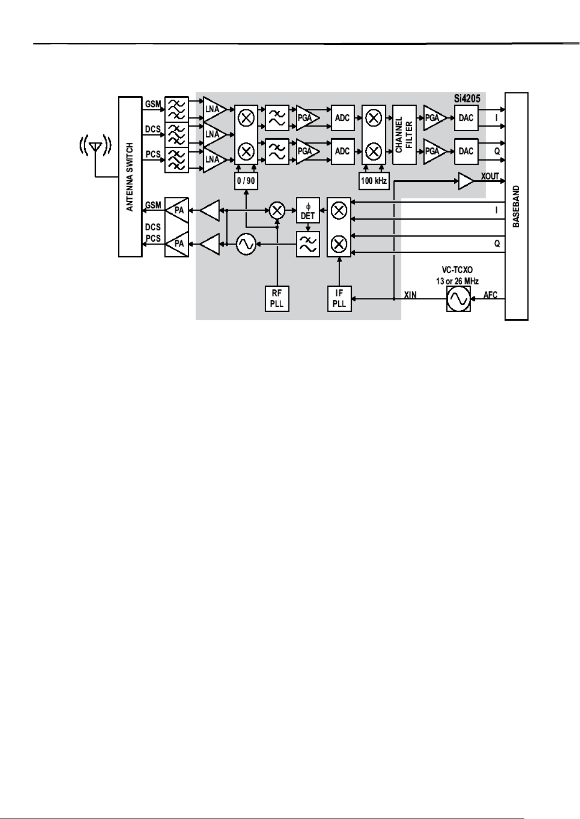
4.2 Radio Transceiver Section
Fig.4-1. RF Transceiver block diagram
The ZEUS’s RF Transceiver, which is AERO, consists of the Si4200 GSM transceiver (U710),
Si4201 universal baseband interface (U702), and Si4133T dual RF synthesizer (U601). The highly
integrated solution eliminates the IF SAW filter, external low noise amplifiers (LNAs) for three bands,
transmit and RF voltage controlled oscillator (VCO) modules, and more than 60 other discrete
components found in conventional designs.
The receive section uses a digital low-IF architecture that avoids the difficulties associated with
direct conversion while delivering lower solution cost and reduced complexity. The universal
baseband interface (U702) is compatible with any supplier’s baseband subsystem.
The transmit section is a complete up-conversion path from the baseband subsystem to the power
amplifer (U701) and uses an offset phase locked loop (PLL) with a fully integrated transmit VCO.
The frequency synthesizer (U601) includes integrated RF and IF VCO’s, Varactors, and Loop filters.
The unique integer-N PLL architecture used in the Si4133T (U601) produces a transient response
that is superior in speed to fractional architectures without suffering the high phase noise or
spurious modulation effects often associated with those designs.
The following Figure shows STYLE’s top view of PCB artworks.
PANTECH R&D CONFIDENTIAL
ZEUS Service Manual
13
Fig.4-2. Top view of RF Transceiver PCB Layout
4.2.1 DC Distribution and Regulation Part
The battery voltage, in return, is applied to the logic part and RF part via LDO(Low Drop-Out)
regulator. As several LDO regulators are used, power can be supplied for each necessary part
efficiently. Audio/Logic parts use +2.8V. Si4205 RF Transceiver (U710) and RF3133 Power Amplifier
(U701) also use +2.8V DC voltage.
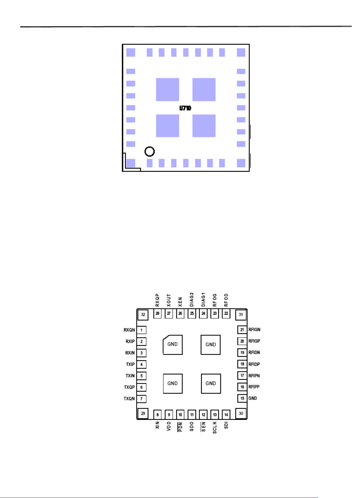
4.2.2 Transciever pin description
Fig.4-3. Top View of Si4205-BM
PANTECH R&D CONFIDENTIAL
ZEUS Service Manual
14
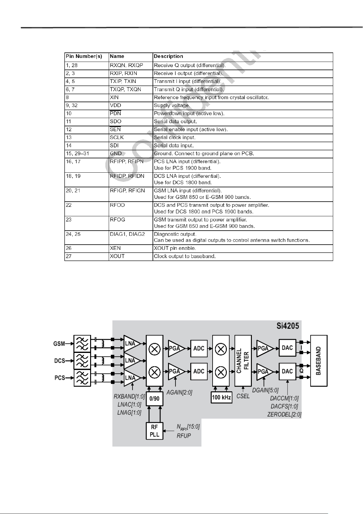
Table 4-1. Pin Description of Si4200DB-BM
4.2.3 Receiver Section
4.2.3.1 An Overview of Receive section
Fig.4-6. Receiver block diagram
PANTECH R&D CONFIDENTIAL
 Loading...